US9201318B2 - Polymer for charge generation layer and charge transport layer formulation - Google Patents
Polymer for charge generation layer and charge transport layer formulation Download PDFInfo
- Publication number
- US9201318B2 US9201318B2 US13/944,813 US201313944813A US9201318B2 US 9201318 B2 US9201318 B2 US 9201318B2 US 201313944813 A US201313944813 A US 201313944813A US 9201318 B2 US9201318 B2 US 9201318B2
- Authority
- US
- United States
- Prior art keywords
- imaging member
- layer
- charge
- charge transport
- transport layer
- Prior art date
- Legal status (The legal status is an assumption and is not a legal conclusion. Google has not performed a legal analysis and makes no representation as to the accuracy of the status listed.)
- Expired - Fee Related, expires
Links
- 239000000203 mixture Substances 0.000 title claims abstract description 44
- 238000009472 formulation Methods 0.000 title abstract description 11
- 229920000642 polymer Polymers 0.000 title description 14
- 238000003384 imaging method Methods 0.000 claims abstract description 198
- 230000015572 biosynthetic process Effects 0.000 claims abstract description 7
- 239000010410 layer Substances 0.000 claims description 313
- 239000000758 substrate Substances 0.000 claims description 73
- 239000000463 material Substances 0.000 claims description 55
- 238000000576 coating method Methods 0.000 claims description 53
- 239000011248 coating agent Substances 0.000 claims description 51
- 239000011230 binding agent Substances 0.000 claims description 45
- 229920000515 polycarbonate Polymers 0.000 claims description 36
- 239000004417 polycarbonate Substances 0.000 claims description 35
- 239000007788 liquid Substances 0.000 claims description 29
- 239000004014 plasticizer Substances 0.000 claims description 29
- 229920001577 copolymer Polymers 0.000 claims description 23
- XNGIFLGASWRNHJ-UHFFFAOYSA-N phthalic acid Chemical compound OC(=O)C1=CC=CC=C1C(O)=O XNGIFLGASWRNHJ-UHFFFAOYSA-N 0.000 claims description 22
- IISBACLAFKSPIT-UHFFFAOYSA-N bisphenol A Chemical compound C=1C=C(O)C=CC=1C(C)(C)C1=CC=C(O)C=C1 IISBACLAFKSPIT-UHFFFAOYSA-N 0.000 claims description 15
- 150000001875 compounds Chemical class 0.000 claims description 12
- 238000011161 development Methods 0.000 claims description 12
- 239000004793 Polystyrene Substances 0.000 claims description 9
- 229920000402 bisphenol A polycarbonate polymer Polymers 0.000 claims description 9
- 229920001400 block copolymer Polymers 0.000 claims description 9
- 238000006116 polymerization reaction Methods 0.000 claims description 9
- 229920002223 polystyrene Polymers 0.000 claims description 9
- 239000011247 coating layer Substances 0.000 claims description 6
- 125000001495 ethyl group Chemical group [H]C([H])([H])C([H])([H])* 0.000 claims description 6
- 238000012546 transfer Methods 0.000 claims description 6
- 230000032798 delamination Effects 0.000 claims description 5
- IYRWEQXVUNLMAY-UHFFFAOYSA-N fluoroketone group Chemical group FC(=O)F IYRWEQXVUNLMAY-UHFFFAOYSA-N 0.000 claims description 5
- 125000005498 phthalate group Chemical class 0.000 claims description 5
- 150000004649 carbonic acid derivatives Chemical class 0.000 claims description 4
- 238000000926 separation method Methods 0.000 claims description 4
- SLMOFSKRLCGLIX-UHFFFAOYSA-N 1-(2,4-dimethoxyphenyl)-2,2,2-trifluoroethanone Chemical compound COC1=CC=C(C(=O)C(F)(F)F)C(OC)=C1 SLMOFSKRLCGLIX-UHFFFAOYSA-N 0.000 claims description 2
- PUSBIOFSWWHNDD-UHFFFAOYSA-N 1-[2-(trifluoromethyl)phenyl]propan-1-one Chemical compound CCC(=O)C1=CC=CC=C1C(F)(F)F PUSBIOFSWWHNDD-UHFFFAOYSA-N 0.000 claims description 2
- MCYCSIKSZLARBD-UHFFFAOYSA-N 1-[3,5-bis(trifluoromethyl)phenyl]ethanone Chemical compound CC(=O)C1=CC(C(F)(F)F)=CC(C(F)(F)F)=C1 MCYCSIKSZLARBD-UHFFFAOYSA-N 0.000 claims description 2
- UBTPNKXHYILGJU-UHFFFAOYSA-N 1-[3-(trifluoromethyl)phenyl]propan-1-one Chemical compound CCC(=O)C1=CC=CC(C(F)(F)F)=C1 UBTPNKXHYILGJU-UHFFFAOYSA-N 0.000 claims description 2
- JPHQCDCEBDRIOL-UHFFFAOYSA-N 1-[3-(trifluoromethyl)phenyl]propan-2-one Chemical compound CC(=O)CC1=CC=CC(C(F)(F)F)=C1 JPHQCDCEBDRIOL-UHFFFAOYSA-N 0.000 claims description 2
- QFKOWENRSZZLPK-UHFFFAOYSA-N 1-[4-(trifluoromethyl)phenyl]propan-1-one Chemical compound CCC(=O)C1=CC=C(C(F)(F)F)C=C1 QFKOWENRSZZLPK-UHFFFAOYSA-N 0.000 claims description 2
- VVXLFFIFNVKFBD-UHFFFAOYSA-N 4,4,4-trifluoro-1-phenylbutane-1,3-dione Chemical compound FC(F)(F)C(=O)CC(=O)C1=CC=CC=C1 VVXLFFIFNVKFBD-UHFFFAOYSA-N 0.000 claims description 2
- JTIPWONXTZMDOK-UHFFFAOYSA-N 4,4-difluoro-1-phenylbutane-1,3-dione Chemical compound FC(F)C(=O)CC(=O)C1=CC=CC=C1 JTIPWONXTZMDOK-UHFFFAOYSA-N 0.000 claims description 2
- 229910052739 hydrogen Inorganic materials 0.000 claims description 2
- 238000004627 transmission electron microscopy Methods 0.000 claims 1
- 238000000034 method Methods 0.000 abstract description 36
- 230000008569 process Effects 0.000 abstract description 26
- 239000002491 polymer binding agent Substances 0.000 abstract description 23
- 229920005596 polymer binder Polymers 0.000 abstract description 22
- -1 polyvinylbutryral Polymers 0.000 description 31
- 229920000359 diblock copolymer Polymers 0.000 description 25
- 230000000903 blocking effect Effects 0.000 description 23
- FLKPEMZONWLCSK-UHFFFAOYSA-N diethyl phthalate Chemical compound CCOC(=O)C1=CC=CC=C1C(=O)OCC FLKPEMZONWLCSK-UHFFFAOYSA-N 0.000 description 20
- YMWUJEATGCHHMB-UHFFFAOYSA-N Dichloromethane Chemical compound ClCCl YMWUJEATGCHHMB-UHFFFAOYSA-N 0.000 description 18
- 239000002245 particle Substances 0.000 description 18
- 230000000694 effects Effects 0.000 description 17
- 125000002496 methyl group Chemical group [H]C([H])([H])* 0.000 description 17
- 239000000243 solution Substances 0.000 description 16
- 230000008602 contraction Effects 0.000 description 15
- 238000001035 drying Methods 0.000 description 14
- 229910052751 metal Inorganic materials 0.000 description 13
- 239000002184 metal Substances 0.000 description 13
- 108091008695 photoreceptors Proteins 0.000 description 12
- 239000000853 adhesive Substances 0.000 description 11
- 230000001070 adhesive effect Effects 0.000 description 11
- PXHVJJICTQNCMI-UHFFFAOYSA-N Nickel Chemical compound [Ni] PXHVJJICTQNCMI-UHFFFAOYSA-N 0.000 description 10
- WYURNTSHIVDZCO-UHFFFAOYSA-N Tetrahydrofuran Chemical compound C1CCOC1 WYURNTSHIVDZCO-UHFFFAOYSA-N 0.000 description 10
- RTAQQCXQSZGOHL-UHFFFAOYSA-N Titanium Chemical compound [Ti] RTAQQCXQSZGOHL-UHFFFAOYSA-N 0.000 description 10
- 125000004432 carbon atom Chemical group C* 0.000 description 10
- 229920005989 resin Polymers 0.000 description 10
- 239000011347 resin Substances 0.000 description 10
- 239000002904 solvent Substances 0.000 description 10
- 238000001816 cooling Methods 0.000 description 9
- 239000006185 dispersion Substances 0.000 description 8
- 238000010348 incorporation Methods 0.000 description 8
- OFOBLEOULBTSOW-UHFFFAOYSA-N Malonic acid Chemical compound OC(=O)CC(O)=O OFOBLEOULBTSOW-UHFFFAOYSA-N 0.000 description 7
- 238000013461 design Methods 0.000 description 7
- 230000006870 function Effects 0.000 description 7
- IEQIEDJGQAUEQZ-UHFFFAOYSA-N phthalocyanine Chemical compound N1C(N=C2C3=CC=CC=C3C(N=C3C4=CC=CC=C4C(=N4)N3)=N2)=C(C=CC=C2)C2=C1N=C1C2=CC=CC=C2C4=N1 IEQIEDJGQAUEQZ-UHFFFAOYSA-N 0.000 description 7
- 238000002360 preparation method Methods 0.000 description 7
- 239000000126 substance Substances 0.000 description 7
- KKEYFWRCBNTPAC-UHFFFAOYSA-N Terephthalic acid Chemical compound OC(=O)C1=CC=C(C(O)=O)C=C1 KKEYFWRCBNTPAC-UHFFFAOYSA-N 0.000 description 6
- 239000012790 adhesive layer Substances 0.000 description 6
- 125000003118 aryl group Chemical group 0.000 description 6
- 150000007524 organic acids Chemical group 0.000 description 6
- 229920000728 polyester Polymers 0.000 description 6
- 230000009467 reduction Effects 0.000 description 6
- 229910052719 titanium Inorganic materials 0.000 description 6
- 239000010936 titanium Substances 0.000 description 6
- 229940117958 vinyl acetate Drugs 0.000 description 6
- VYZAMTAEIAYCRO-UHFFFAOYSA-N Chromium Chemical compound [Cr] VYZAMTAEIAYCRO-UHFFFAOYSA-N 0.000 description 5
- 229920004142 LEXAN™ Polymers 0.000 description 5
- 239000004418 Lexan Substances 0.000 description 5
- 239000004952 Polyamide Substances 0.000 description 5
- BUGBHKTXTAQXES-UHFFFAOYSA-N Selenium Chemical compound [Se] BUGBHKTXTAQXES-UHFFFAOYSA-N 0.000 description 5
- BZHJMEDXRYGGRV-UHFFFAOYSA-N Vinyl chloride Chemical compound ClC=C BZHJMEDXRYGGRV-UHFFFAOYSA-N 0.000 description 5
- 238000005299 abrasion Methods 0.000 description 5
- 125000000217 alkyl group Chemical group 0.000 description 5
- 229910052782 aluminium Inorganic materials 0.000 description 5
- XAGFODPZIPBFFR-UHFFFAOYSA-N aluminium Chemical compound [Al] XAGFODPZIPBFFR-UHFFFAOYSA-N 0.000 description 5
- 229910052804 chromium Inorganic materials 0.000 description 5
- 239000011651 chromium Substances 0.000 description 5
- 238000007796 conventional method Methods 0.000 description 5
- 230000007547 defect Effects 0.000 description 5
- 238000002347 injection Methods 0.000 description 5
- 239000007924 injection Substances 0.000 description 5
- 238000004519 manufacturing process Methods 0.000 description 5
- 150000002739 metals Chemical class 0.000 description 5
- 229910052759 nickel Inorganic materials 0.000 description 5
- 239000000123 paper Substances 0.000 description 5
- 239000000049 pigment Substances 0.000 description 5
- 229920002647 polyamide Polymers 0.000 description 5
- 230000005855 radiation Effects 0.000 description 5
- 239000007787 solid Substances 0.000 description 5
- YLQBMQCUIZJEEH-UHFFFAOYSA-N tetrahydrofuran Natural products C=1C=COC=1 YLQBMQCUIZJEEH-UHFFFAOYSA-N 0.000 description 5
- 125000006273 (C1-C3) alkyl group Chemical group 0.000 description 4
- OKTJSMMVPCPJKN-UHFFFAOYSA-N Carbon Chemical compound [C] OKTJSMMVPCPJKN-UHFFFAOYSA-N 0.000 description 4
- 239000004642 Polyimide Substances 0.000 description 4
- QCWXUUIWCKQGHC-UHFFFAOYSA-N Zirconium Chemical compound [Zr] QCWXUUIWCKQGHC-UHFFFAOYSA-N 0.000 description 4
- 230000003213 activating effect Effects 0.000 description 4
- 229920000180 alkyd Polymers 0.000 description 4
- 230000008901 benefit Effects 0.000 description 4
- 239000004305 biphenyl Substances 0.000 description 4
- 239000004020 conductor Substances 0.000 description 4
- 230000009977 dual effect Effects 0.000 description 4
- 238000001125 extrusion Methods 0.000 description 4
- 229910002804 graphite Inorganic materials 0.000 description 4
- 239000010439 graphite Substances 0.000 description 4
- AMGQUBHHOARCQH-UHFFFAOYSA-N indium;oxotin Chemical compound [In].[Sn]=O AMGQUBHHOARCQH-UHFFFAOYSA-N 0.000 description 4
- 150000004706 metal oxides Chemical group 0.000 description 4
- 238000012986 modification Methods 0.000 description 4
- 230000004048 modification Effects 0.000 description 4
- 229910052758 niobium Inorganic materials 0.000 description 4
- 239000010955 niobium Substances 0.000 description 4
- GUCVJGMIXFAOAE-UHFFFAOYSA-N niobium atom Chemical compound [Nb] GUCVJGMIXFAOAE-UHFFFAOYSA-N 0.000 description 4
- SJHHDDDGXWOYOE-UHFFFAOYSA-N oxytitamium phthalocyanine Chemical compound [Ti+2]=O.C12=CC=CC=C2C(N=C2[N-]C(C3=CC=CC=C32)=N2)=NC1=NC([C]1C=CC=CC1=1)=NC=1N=C1[C]3C=CC=CC3=C2[N-]1 SJHHDDDGXWOYOE-UHFFFAOYSA-N 0.000 description 4
- 229920000058 polyacrylate Polymers 0.000 description 4
- 229920001230 polyarylate Polymers 0.000 description 4
- 229920000647 polyepoxide Polymers 0.000 description 4
- 239000011112 polyethylene naphthalate Substances 0.000 description 4
- 229920000139 polyethylene terephthalate Polymers 0.000 description 4
- 239000005020 polyethylene terephthalate Substances 0.000 description 4
- 229920001721 polyimide Polymers 0.000 description 4
- 229920001296 polysiloxane Polymers 0.000 description 4
- 229920002635 polyurethane Polymers 0.000 description 4
- 239000004814 polyurethane Substances 0.000 description 4
- 125000006413 ring segment Chemical group 0.000 description 4
- 229910052711 selenium Inorganic materials 0.000 description 4
- 239000011669 selenium Substances 0.000 description 4
- 239000006104 solid solution Substances 0.000 description 4
- 229910001220 stainless steel Inorganic materials 0.000 description 4
- 239000010935 stainless steel Substances 0.000 description 4
- 229910052726 zirconium Inorganic materials 0.000 description 4
- 125000004169 (C1-C6) alkyl group Chemical group 0.000 description 3
- KIIFVSJBFGYDFV-UHFFFAOYSA-N 1h-benzimidazole;perylene Chemical group C1=CC=C2NC=NC2=C1.C1=CC(C2=CC=CC=3C2=C2C=CC=3)=C3C2=CC=CC3=C1 KIIFVSJBFGYDFV-UHFFFAOYSA-N 0.000 description 3
- QTBSBXVTEAMEQO-UHFFFAOYSA-N Acetic acid Chemical compound CC(O)=O QTBSBXVTEAMEQO-UHFFFAOYSA-N 0.000 description 3
- BVKZGUZCCUSVTD-UHFFFAOYSA-L Carbonate Chemical compound [O-]C([O-])=O BVKZGUZCCUSVTD-UHFFFAOYSA-L 0.000 description 3
- YXFVVABEGXRONW-UHFFFAOYSA-N Toluene Chemical compound CC1=CC=CC=C1 YXFVVABEGXRONW-UHFFFAOYSA-N 0.000 description 3
- 239000002253 acid Substances 0.000 description 3
- 239000000654 additive Substances 0.000 description 3
- 125000003545 alkoxy group Chemical group 0.000 description 3
- 150000004982 aromatic amines Chemical class 0.000 description 3
- 238000009835 boiling Methods 0.000 description 3
- 239000002131 composite material Substances 0.000 description 3
- 238000000151 deposition Methods 0.000 description 3
- 238000003618 dip coating Methods 0.000 description 3
- 230000008030 elimination Effects 0.000 description 3
- 238000003379 elimination reaction Methods 0.000 description 3
- 239000003822 epoxy resin Substances 0.000 description 3
- 238000007765 extrusion coating Methods 0.000 description 3
- 125000001153 fluoro group Chemical group F* 0.000 description 3
- 230000009477 glass transition Effects 0.000 description 3
- 229910052736 halogen Inorganic materials 0.000 description 3
- 150000002367 halogens Chemical class 0.000 description 3
- LNEPOXFFQSENCJ-UHFFFAOYSA-N haloperidol Chemical compound C1CC(O)(C=2C=CC(Cl)=CC=2)CCN1CCCC(=O)C1=CC=C(F)C=C1 LNEPOXFFQSENCJ-UHFFFAOYSA-N 0.000 description 3
- 230000006872 improvement Effects 0.000 description 3
- 125000001449 isopropyl group Chemical group [H]C([H])([H])C([H])(*)C([H])([H])[H] 0.000 description 3
- 230000000670 limiting effect Effects 0.000 description 3
- 239000011159 matrix material Substances 0.000 description 3
- 229910044991 metal oxide Inorganic materials 0.000 description 3
- 229910052757 nitrogen Inorganic materials 0.000 description 3
- 230000003287 optical effect Effects 0.000 description 3
- 229920000620 organic polymer Polymers 0.000 description 3
- 125000001997 phenyl group Chemical group [H]C1=C([H])C([H])=C(*)C([H])=C1[H] 0.000 description 3
- 229920003207 poly(ethylene-2,6-naphthalate) Polymers 0.000 description 3
- 229920002037 poly(vinyl butyral) polymer Polymers 0.000 description 3
- 230000002028 premature Effects 0.000 description 3
- 230000035945 sensitivity Effects 0.000 description 3
- 239000002002 slurry Substances 0.000 description 3
- 238000005507 spraying Methods 0.000 description 3
- 150000003440 styrenes Chemical class 0.000 description 3
- 229910052715 tantalum Inorganic materials 0.000 description 3
- GUVRBAGPIYLISA-UHFFFAOYSA-N tantalum atom Chemical compound [Ta] GUVRBAGPIYLISA-UHFFFAOYSA-N 0.000 description 3
- 238000012360 testing method Methods 0.000 description 3
- 229920001169 thermoplastic Polymers 0.000 description 3
- 239000004416 thermosoftening plastic Substances 0.000 description 3
- 229910052720 vanadium Inorganic materials 0.000 description 3
- GPPXJZIENCGNKB-UHFFFAOYSA-N vanadium Chemical compound [V]#[V] GPPXJZIENCGNKB-UHFFFAOYSA-N 0.000 description 3
- 229920002554 vinyl polymer Polymers 0.000 description 3
- XLYOFNOQVPJJNP-UHFFFAOYSA-N water Substances O XLYOFNOQVPJJNP-UHFFFAOYSA-N 0.000 description 3
- OGGKVJMNFFSDEV-UHFFFAOYSA-N 3-methyl-n-[4-[4-(n-(3-methylphenyl)anilino)phenyl]phenyl]-n-phenylaniline Chemical group CC1=CC=CC(N(C=2C=CC=CC=2)C=2C=CC(=CC=2)C=2C=CC(=CC=2)N(C=2C=CC=CC=2)C=2C=C(C)C=CC=2)=C1 OGGKVJMNFFSDEV-UHFFFAOYSA-N 0.000 description 2
- MVIXNQZIMMIGEL-UHFFFAOYSA-N 4-methyl-n-[4-[4-(4-methyl-n-(4-methylphenyl)anilino)phenyl]phenyl]-n-(4-methylphenyl)aniline Chemical compound C1=CC(C)=CC=C1N(C=1C=CC(=CC=1)C=1C=CC(=CC=1)N(C=1C=CC(C)=CC=1)C=1C=CC(C)=CC=1)C1=CC=C(C)C=C1 MVIXNQZIMMIGEL-UHFFFAOYSA-N 0.000 description 2
- OMIHGPLIXGGMJB-UHFFFAOYSA-N 7-oxabicyclo[4.1.0]hepta-1,3,5-triene Chemical compound C1=CC=C2OC2=C1 OMIHGPLIXGGMJB-UHFFFAOYSA-N 0.000 description 2
- SDDLEVPIDBLVHC-UHFFFAOYSA-N Bisphenol Z Chemical compound C1=CC(O)=CC=C1C1(C=2C=CC(O)=CC=2)CCCCC1 SDDLEVPIDBLVHC-UHFFFAOYSA-N 0.000 description 2
- 229920002799 BoPET Polymers 0.000 description 2
- 229910001369 Brass Inorganic materials 0.000 description 2
- RYGMFSIKBFXOCR-UHFFFAOYSA-N Copper Chemical compound [Cu] RYGMFSIKBFXOCR-UHFFFAOYSA-N 0.000 description 2
- XDTMQSROBMDMFD-UHFFFAOYSA-N Cyclohexane Chemical compound C1CCCCC1 XDTMQSROBMDMFD-UHFFFAOYSA-N 0.000 description 2
- ZOKXTWBITQBERF-UHFFFAOYSA-N Molybdenum Chemical compound [Mo] ZOKXTWBITQBERF-UHFFFAOYSA-N 0.000 description 2
- IMNFDUFMRHMDMM-UHFFFAOYSA-N N-Heptane Chemical compound CCCCCCC IMNFDUFMRHMDMM-UHFFFAOYSA-N 0.000 description 2
- 239000004698 Polyethylene Substances 0.000 description 2
- 239000004734 Polyphenylene sulfide Substances 0.000 description 2
- 239000004743 Polypropylene Substances 0.000 description 2
- WCUXLLCKKVVCTQ-UHFFFAOYSA-M Potassium chloride Chemical compound [Cl-].[K+] WCUXLLCKKVVCTQ-UHFFFAOYSA-M 0.000 description 2
- 229910001370 Se alloy Inorganic materials 0.000 description 2
- VYPSYNLAJGMNEJ-UHFFFAOYSA-N Silicium dioxide Chemical compound O=[Si]=O VYPSYNLAJGMNEJ-UHFFFAOYSA-N 0.000 description 2
- BQCADISMDOOEFD-UHFFFAOYSA-N Silver Chemical compound [Ag] BQCADISMDOOEFD-UHFFFAOYSA-N 0.000 description 2
- 150000001241 acetals Chemical class 0.000 description 2
- 230000000996 additive effect Effects 0.000 description 2
- WNLRTRBMVRJNCN-UHFFFAOYSA-N adipic acid Chemical compound OC(=O)CCCCC(O)=O WNLRTRBMVRJNCN-UHFFFAOYSA-N 0.000 description 2
- 238000007605 air drying Methods 0.000 description 2
- 125000001931 aliphatic group Chemical group 0.000 description 2
- 125000002947 alkylene group Chemical group 0.000 description 2
- 229920003180 amino resin Polymers 0.000 description 2
- 239000010951 brass Substances 0.000 description 2
- 125000000484 butyl group Chemical group [H]C([*])([H])C([H])([H])C([H])([H])C([H])([H])[H] 0.000 description 2
- MVPPADPHJFYWMZ-UHFFFAOYSA-N chlorobenzene Chemical compound ClC1=CC=CC=C1 MVPPADPHJFYWMZ-UHFFFAOYSA-N 0.000 description 2
- 238000004140 cleaning Methods 0.000 description 2
- 230000000295 complement effect Effects 0.000 description 2
- 229910052802 copper Inorganic materials 0.000 description 2
- 239000010949 copper Substances 0.000 description 2
- 125000004122 cyclic group Chemical group 0.000 description 2
- 230000001351 cycling effect Effects 0.000 description 2
- JHIVVAPYMSGYDF-UHFFFAOYSA-N cyclohexanone Chemical compound O=C1CCCCC1 JHIVVAPYMSGYDF-UHFFFAOYSA-N 0.000 description 2
- 125000000113 cyclohexyl group Chemical group [H]C1([H])C([H])([H])C([H])([H])C([H])(*)C([H])([H])C1([H])[H] 0.000 description 2
- 230000008021 deposition Effects 0.000 description 2
- 150000004985 diamines Chemical class 0.000 description 2
- 230000005670 electromagnetic radiation Effects 0.000 description 2
- 239000007789 gas Substances 0.000 description 2
- 239000011521 glass Substances 0.000 description 2
- PCHJSUWPFVWCPO-UHFFFAOYSA-N gold Chemical compound [Au] PCHJSUWPFVWCPO-UHFFFAOYSA-N 0.000 description 2
- 229910052737 gold Inorganic materials 0.000 description 2
- 239000010931 gold Substances 0.000 description 2
- 229910052735 hafnium Inorganic materials 0.000 description 2
- VBJZVLUMGGDVMO-UHFFFAOYSA-N hafnium atom Chemical compound [Hf] VBJZVLUMGGDVMO-UHFFFAOYSA-N 0.000 description 2
- 125000001188 haloalkyl group Chemical group 0.000 description 2
- 238000010438 heat treatment Methods 0.000 description 2
- 230000005525 hole transport Effects 0.000 description 2
- 238000005286 illumination Methods 0.000 description 2
- 229910010272 inorganic material Inorganic materials 0.000 description 2
- 239000011147 inorganic material Substances 0.000 description 2
- 239000012212 insulator Substances 0.000 description 2
- 230000003993 interaction Effects 0.000 description 2
- 230000001788 irregular Effects 0.000 description 2
- QQVIHTHCMHWDBS-UHFFFAOYSA-N isophthalic acid Chemical compound OC(=O)C1=CC=CC(C(O)=O)=C1 QQVIHTHCMHWDBS-UHFFFAOYSA-N 0.000 description 2
- 238000002156 mixing Methods 0.000 description 2
- 229910052750 molybdenum Inorganic materials 0.000 description 2
- 239000011733 molybdenum Substances 0.000 description 2
- BDJRBEYXGGNYIS-UHFFFAOYSA-N nonanedioic acid Chemical compound OC(=O)CCCCCCCC(O)=O BDJRBEYXGGNYIS-UHFFFAOYSA-N 0.000 description 2
- 239000011368 organic material Substances 0.000 description 2
- 238000000643 oven drying Methods 0.000 description 2
- 229920001568 phenolic resin Polymers 0.000 description 2
- 239000005011 phenolic resin Substances 0.000 description 2
- WLJVNTCWHIRURA-UHFFFAOYSA-N pimelic acid Chemical compound OC(=O)CCCCCC(O)=O WLJVNTCWHIRURA-UHFFFAOYSA-N 0.000 description 2
- 229920003023 plastic Polymers 0.000 description 2
- 239000004033 plastic Substances 0.000 description 2
- 229920000090 poly(aryl ether) Polymers 0.000 description 2
- 229920002492 poly(sulfone) Polymers 0.000 description 2
- 229920002857 polybutadiene Polymers 0.000 description 2
- 229920006393 polyether sulfone Polymers 0.000 description 2
- 229920000573 polyethylene Polymers 0.000 description 2
- 229920000306 polymethylpentene Polymers 0.000 description 2
- 229920000069 polyphenylene sulfide Polymers 0.000 description 2
- 229920001155 polypropylene Polymers 0.000 description 2
- 229920001343 polytetrafluoroethylene Polymers 0.000 description 2
- 239000004810 polytetrafluoroethylene Substances 0.000 description 2
- 229920002689 polyvinyl acetate Polymers 0.000 description 2
- 229920000915 polyvinyl chloride Polymers 0.000 description 2
- 125000002924 primary amino group Chemical group [H]N([H])* 0.000 description 2
- 125000001436 propyl group Chemical group [H]C([*])([H])C([H])([H])C([H])([H])[H] 0.000 description 2
- CXMXRPHRNRROMY-UHFFFAOYSA-N sebacic acid Chemical compound OC(=O)CCCCCCCCC(O)=O CXMXRPHRNRROMY-UHFFFAOYSA-N 0.000 description 2
- 229910052709 silver Inorganic materials 0.000 description 2
- 239000004332 silver Substances 0.000 description 2
- 239000002356 single layer Substances 0.000 description 2
- 239000011877 solvent mixture Substances 0.000 description 2
- 230000002269 spontaneous effect Effects 0.000 description 2
- 229920003048 styrene butadiene rubber Polymers 0.000 description 2
- TYFQFVWCELRYAO-UHFFFAOYSA-N suberic acid Chemical compound OC(=O)CCCCCCC(O)=O TYFQFVWCELRYAO-UHFFFAOYSA-N 0.000 description 2
- 230000001629 suppression Effects 0.000 description 2
- WFKWXMTUELFFGS-UHFFFAOYSA-N tungsten Chemical compound [W] WFKWXMTUELFFGS-UHFFFAOYSA-N 0.000 description 2
- 229910052721 tungsten Inorganic materials 0.000 description 2
- 239000010937 tungsten Substances 0.000 description 2
- WYTZZXDRDKSJID-UHFFFAOYSA-N (3-aminopropyl)triethoxysilane Chemical compound CCO[Si](OCC)(OCC)CCCN WYTZZXDRDKSJID-UHFFFAOYSA-N 0.000 description 1
- 125000004191 (C1-C6) alkoxy group Chemical group 0.000 description 1
- RTBFRGCFXZNCOE-UHFFFAOYSA-N 1-methylsulfonylpiperidin-4-one Chemical compound CS(=O)(=O)N1CCC(=O)CC1 RTBFRGCFXZNCOE-UHFFFAOYSA-N 0.000 description 1
- XDOFQFKRPWOURC-UHFFFAOYSA-N 16-methylheptadecanoic acid Chemical compound CC(C)CCCCCCCCCCCCCCC(O)=O XDOFQFKRPWOURC-UHFFFAOYSA-N 0.000 description 1
- OFAPSLLQSSHRSQ-UHFFFAOYSA-N 1H-triazine-2,4-diamine Chemical class NN1NC=CC(N)=N1 OFAPSLLQSSHRSQ-UHFFFAOYSA-N 0.000 description 1
- JHQVCQDWGSXTFE-UHFFFAOYSA-N 2-(2-prop-2-enoxycarbonyloxyethoxy)ethyl prop-2-enyl carbonate Chemical compound C=CCOC(=O)OCCOCCOC(=O)OCC=C JHQVCQDWGSXTFE-UHFFFAOYSA-N 0.000 description 1
- OEPOKWHJYJXUGD-UHFFFAOYSA-N 2-(3-phenylmethoxyphenyl)-1,3-thiazole-4-carbaldehyde Chemical compound O=CC1=CSC(C=2C=C(OCC=3C=CC=CC=3)C=CC=2)=N1 OEPOKWHJYJXUGD-UHFFFAOYSA-N 0.000 description 1
- NGXPSFCDNMDGCI-UHFFFAOYSA-N 2-chloro-n-[4-[4-(n-(2-chlorophenyl)anilino)phenyl]phenyl]-n-phenylaniline Chemical compound ClC1=CC=CC=C1N(C=1C=CC(=CC=1)C=1C=CC(=CC=1)N(C=1C=CC=CC=1)C=1C(=CC=CC=1)Cl)C1=CC=CC=C1 NGXPSFCDNMDGCI-UHFFFAOYSA-N 0.000 description 1
- MEPWMMZGWMVZOH-UHFFFAOYSA-N 2-n-trimethoxysilylpropane-1,2-diamine Chemical compound CO[Si](OC)(OC)NC(C)CN MEPWMMZGWMVZOH-UHFFFAOYSA-N 0.000 description 1
- HXLAEGYMDGUSBD-UHFFFAOYSA-N 3-[diethoxy(methyl)silyl]propan-1-amine Chemical compound CCO[Si](C)(OCC)CCCN HXLAEGYMDGUSBD-UHFFFAOYSA-N 0.000 description 1
- OVFXQPOXNVQNSJ-UHFFFAOYSA-N 3-chloro-n-[4-[4-(n-(3-chlorophenyl)anilino)-4-phenylcyclohexa-1,5-dien-1-yl]phenyl]-n-phenylaniline Chemical compound ClC1=CC=CC(N(C=2C=CC=CC=2)C=2C=CC(=CC=2)C=2C=CC(CC=2)(N(C=2C=CC=CC=2)C=2C=C(Cl)C=CC=2)C=2C=CC=CC=2)=C1 OVFXQPOXNVQNSJ-UHFFFAOYSA-N 0.000 description 1
- SJECZPVISLOESU-UHFFFAOYSA-N 3-trimethoxysilylpropan-1-amine Chemical compound CO[Si](OC)(OC)CCCN SJECZPVISLOESU-UHFFFAOYSA-N 0.000 description 1
- BMKOVBATNIFKNA-UHFFFAOYSA-N 4-[diethoxy(methyl)silyl]butan-2-amine Chemical compound CCO[Si](C)(OCC)CCC(C)N BMKOVBATNIFKNA-UHFFFAOYSA-N 0.000 description 1
- GBIDVAHDYHDYFG-UHFFFAOYSA-J 4-aminobenzoate titanium(4+) Chemical compound [Ti+4].Nc1ccc(cc1)C([O-])=O.Nc1ccc(cc1)C([O-])=O.Nc1ccc(cc1)C([O-])=O.Nc1ccc(cc1)C([O-])=O GBIDVAHDYHDYFG-UHFFFAOYSA-J 0.000 description 1
- SRRPHAPPCGRQKB-UHFFFAOYSA-N 4-aminobenzoic acid;16-methylheptadecanoic acid;propan-2-ol;titanium Chemical compound [Ti].CC(C)O.NC1=CC=C(C(O)=O)C=C1.NC1=CC=C(C(O)=O)C=C1.CC(C)CCCCCCCCCCCCCCC(O)=O SRRPHAPPCGRQKB-UHFFFAOYSA-N 0.000 description 1
- ZSLIEZOEYNOWCL-UHFFFAOYSA-N 4-butyl-n-[4-[4-(4-butyl-n-(4-propan-2-ylphenyl)anilino)-4-phenylcyclohexa-1,5-dien-1-yl]phenyl]-n-(4-propan-2-ylphenyl)aniline Chemical compound C1=CC(CCCC)=CC=C1N(C=1C=CC(=CC=1)C=1C=CC(CC=1)(N(C=1C=CC(CCCC)=CC=1)C=1C=CC(=CC=1)C(C)C)C=1C=CC=CC=1)C1=CC=C(C(C)C)C=C1 ZSLIEZOEYNOWCL-UHFFFAOYSA-N 0.000 description 1
- 229930185605 Bisphenol Natural products 0.000 description 1
- CPELXLSAUQHCOX-UHFFFAOYSA-M Bromide Chemical compound [Br-] CPELXLSAUQHCOX-UHFFFAOYSA-M 0.000 description 1
- VEXZGXHMUGYJMC-UHFFFAOYSA-M Chloride anion Chemical compound [Cl-] VEXZGXHMUGYJMC-UHFFFAOYSA-M 0.000 description 1
- 229920001634 Copolyester Polymers 0.000 description 1
- 239000004593 Epoxy Substances 0.000 description 1
- LFQSCWFLJHTTHZ-UHFFFAOYSA-N Ethanol Chemical compound CCO LFQSCWFLJHTTHZ-UHFFFAOYSA-N 0.000 description 1
- 239000001856 Ethyl cellulose Substances 0.000 description 1
- ZZSNKZQZMQGXPY-UHFFFAOYSA-N Ethyl cellulose Chemical compound CCOCC1OC(OC)C(OCC)C(OCC)C1OC1C(O)C(O)C(OC)C(CO)O1 ZZSNKZQZMQGXPY-UHFFFAOYSA-N 0.000 description 1
- KRHYYFGTRYWZRS-UHFFFAOYSA-M Fluoride anion Chemical compound [F-] KRHYYFGTRYWZRS-UHFFFAOYSA-M 0.000 description 1
- 239000004420 Iupilon Substances 0.000 description 1
- 239000004425 Makrolon Substances 0.000 description 1
- 206010027146 Melanoderma Diseases 0.000 description 1
- 239000005041 Mylar™ Substances 0.000 description 1
- 229920000305 Nylon 6,10 Polymers 0.000 description 1
- BLRPTPMANUNPDV-UHFFFAOYSA-N Silane Chemical compound [SiH4] BLRPTPMANUNPDV-UHFFFAOYSA-N 0.000 description 1
- 229910000831 Steel Inorganic materials 0.000 description 1
- ATJFFYVFTNAWJD-UHFFFAOYSA-N Tin Chemical compound [Sn] ATJFFYVFTNAWJD-UHFFFAOYSA-N 0.000 description 1
- XTXRWKRVRITETP-UHFFFAOYSA-N Vinyl acetate Chemical compound CC(=O)OC=C XTXRWKRVRITETP-UHFFFAOYSA-N 0.000 description 1
- 229920001986 Vinylidene chloride-vinyl chloride copolymer Polymers 0.000 description 1
- HCHKCACWOHOZIP-UHFFFAOYSA-N Zinc Chemical compound [Zn] HCHKCACWOHOZIP-UHFFFAOYSA-N 0.000 description 1
- 239000002318 adhesion promoter Substances 0.000 description 1
- 238000004026 adhesive bonding Methods 0.000 description 1
- 239000001361 adipic acid Substances 0.000 description 1
- 235000011037 adipic acid Nutrition 0.000 description 1
- 230000002411 adverse Effects 0.000 description 1
- 238000007754 air knife coating Methods 0.000 description 1
- 150000004703 alkoxides Chemical class 0.000 description 1
- 229920005603 alternating copolymer Polymers 0.000 description 1
- JFCQEDHGNNZCLN-UHFFFAOYSA-N anhydrous glutaric acid Natural products OC(=O)CCCC(O)=O JFCQEDHGNNZCLN-UHFFFAOYSA-N 0.000 description 1
- KPTXLCRDMLKUHK-UHFFFAOYSA-N aniline;titanium Chemical compound [Ti].NC1=CC=CC=C1 KPTXLCRDMLKUHK-UHFFFAOYSA-N 0.000 description 1
- 238000013459 approach Methods 0.000 description 1
- 238000000149 argon plasma sintering Methods 0.000 description 1
- 229910052785 arsenic Inorganic materials 0.000 description 1
- 230000004888 barrier function Effects 0.000 description 1
- 229940077388 benzenesulfonate Drugs 0.000 description 1
- HFACYLZERDEVSX-UHFFFAOYSA-N benzidine Chemical compound C1=CC(N)=CC=C1C1=CC=C(N)C=C1 HFACYLZERDEVSX-UHFFFAOYSA-N 0.000 description 1
- 230000005540 biological transmission Effects 0.000 description 1
- 229910052793 cadmium Inorganic materials 0.000 description 1
- BDOSMKKIYDKNTQ-UHFFFAOYSA-N cadmium atom Chemical compound [Cd] BDOSMKKIYDKNTQ-UHFFFAOYSA-N 0.000 description 1
- 239000006229 carbon black Substances 0.000 description 1
- 125000005587 carbonate group Chemical group 0.000 description 1
- 229920002678 cellulose Polymers 0.000 description 1
- 239000001913 cellulose Substances 0.000 description 1
- 230000005591 charge neutralization Effects 0.000 description 1
- XOYLJNJLGBYDTH-UHFFFAOYSA-M chlorogallium Chemical compound [Ga]Cl XOYLJNJLGBYDTH-UHFFFAOYSA-M 0.000 description 1
- 239000000084 colloidal system Substances 0.000 description 1
- 229920000891 common polymer Polymers 0.000 description 1
- 230000003750 conditioning effect Effects 0.000 description 1
- 238000007334 copolymerization reaction Methods 0.000 description 1
- 238000005336 cracking Methods 0.000 description 1
- 239000013078 crystal Substances 0.000 description 1
- 230000007812 deficiency Effects 0.000 description 1
- 230000002939 deleterious effect Effects 0.000 description 1
- 239000011928 denatured alcohol Substances 0.000 description 1
- 150000001991 dicarboxylic acids Chemical class 0.000 description 1
- 239000012153 distilled water Substances 0.000 description 1
- 239000002355 dual-layer Substances 0.000 description 1
- 229920001971 elastomer Polymers 0.000 description 1
- 125000003700 epoxy group Chemical group 0.000 description 1
- 125000004185 ester group Chemical group 0.000 description 1
- 229920001249 ethyl cellulose Polymers 0.000 description 1
- 235000019325 ethyl cellulose Nutrition 0.000 description 1
- 238000001704 evaporation Methods 0.000 description 1
- 230000008020 evaporation Effects 0.000 description 1
- 229910052733 gallium Inorganic materials 0.000 description 1
- 238000007756 gravure coating Methods 0.000 description 1
- RBTKNAXYKSUFRK-UHFFFAOYSA-N heliogen blue Chemical compound [Cu].[N-]1C2=C(C=CC=C3)C3=C1N=C([N-]1)C3=CC=CC=C3C1=NC([N-]1)=C(C=CC=C3)C3=C1N=C([N-]1)C3=CC=CC=C3C1=N2 RBTKNAXYKSUFRK-UHFFFAOYSA-N 0.000 description 1
- 125000000623 heterocyclic group Chemical group 0.000 description 1
- XMBWDFGMSWQBCA-UHFFFAOYSA-N hydrogen iodide Chemical compound I XMBWDFGMSWQBCA-UHFFFAOYSA-N 0.000 description 1
- 230000003116 impacting effect Effects 0.000 description 1
- 229910052738 indium Inorganic materials 0.000 description 1
- APFVFJFRJDLVQX-UHFFFAOYSA-N indium atom Chemical compound [In] APFVFJFRJDLVQX-UHFFFAOYSA-N 0.000 description 1
- 229920000592 inorganic polymer Polymers 0.000 description 1
- 239000011810 insulating material Substances 0.000 description 1
- 229910000765 intermetallic Inorganic materials 0.000 description 1
- 230000031700 light absorption Effects 0.000 description 1
- 230000014759 maintenance of location Effects 0.000 description 1
- 230000005226 mechanical processes and functions Effects 0.000 description 1
- 230000007246 mechanism Effects 0.000 description 1
- 229910001092 metal group alloy Inorganic materials 0.000 description 1
- VNWKTOKETHGBQD-UHFFFAOYSA-N methane Chemical compound C VNWKTOKETHGBQD-UHFFFAOYSA-N 0.000 description 1
- PRMHOXAMWFXGCO-UHFFFAOYSA-M molport-000-691-708 Chemical compound N1=C(C2=CC=CC=C2C2=NC=3C4=CC=CC=C4C(=N4)N=3)N2[Ga](Cl)N2C4=C(C=CC=C3)C3=C2N=C2C3=CC=CC=C3C1=N2 PRMHOXAMWFXGCO-UHFFFAOYSA-M 0.000 description 1
- IZIQYHDAXYDQHR-UHFFFAOYSA-N n'-propyl-n'-trimethoxysilylethane-1,2-diamine Chemical compound CCCN(CCN)[Si](OC)(OC)OC IZIQYHDAXYDQHR-UHFFFAOYSA-N 0.000 description 1
- CUHLLYPZXLBADA-UHFFFAOYSA-N n-(4-butylphenyl)-n-[4-[4-(n-(4-butylphenyl)-4-methylanilino)-4-phenylcyclohexa-1,5-dien-1-yl]phenyl]-4-methylaniline Chemical compound C1=CC(CCCC)=CC=C1N(C=1C=CC(=CC=1)C=1C=CC(CC=1)(N(C=1C=CC(C)=CC=1)C=1C=CC(CCCC)=CC=1)C=1C=CC=CC=1)C1=CC=C(C)C=C1 CUHLLYPZXLBADA-UHFFFAOYSA-N 0.000 description 1
- GJXJFORUMJEJPV-UHFFFAOYSA-N n-[4-[4-(4-butyl-n-(2,5-dimethylphenyl)anilino)-4-phenylcyclohexa-1,5-dien-1-yl]phenyl]-n-(4-butylphenyl)-2,5-dimethylaniline Chemical compound C1=CC(CCCC)=CC=C1N(C=1C(=CC=C(C)C=1)C)C1=CC=C(C=2C=CC(CC=2)(N(C=2C=CC(CCCC)=CC=2)C=2C(=CC=C(C)C=2)C)C=2C=CC=CC=2)C=C1 GJXJFORUMJEJPV-UHFFFAOYSA-N 0.000 description 1
- XMJZXKUEAZLKGP-UHFFFAOYSA-N n-[4-[4-(4-butyl-n-(2-ethyl-6-methylphenyl)anilino)-4-phenylcyclohexa-1,5-dien-1-yl]phenyl]-n-(4-butylphenyl)-2-ethyl-6-methylaniline Chemical compound C1=CC(CCCC)=CC=C1N(C=1C(=CC=CC=1C)CC)C1=CC=C(C=2C=CC(CC=2)(N(C=2C=CC(CCCC)=CC=2)C=2C(=CC=CC=2C)CC)C=2C=CC=CC=2)C=C1 XMJZXKUEAZLKGP-UHFFFAOYSA-N 0.000 description 1
- NCHWIKVGNQGHLZ-UHFFFAOYSA-N n-[4-[4-(4-butyl-n-(2-methylphenyl)anilino)-4-phenylcyclohexa-1,5-dien-1-yl]phenyl]-n-(4-butylphenyl)-2-methylaniline Chemical compound C1=CC(CCCC)=CC=C1N(C=1C(=CC=CC=1)C)C1=CC=C(C=2C=CC(CC=2)(N(C=2C=CC(CCCC)=CC=2)C=2C(=CC=CC=2)C)C=2C=CC=CC=2)C=C1 NCHWIKVGNQGHLZ-UHFFFAOYSA-N 0.000 description 1
- SXQXVEKXOYDTRL-UHFFFAOYSA-N n-[4-[4-(4-butyl-n-(3-methylphenyl)anilino)-4-phenylcyclohexa-1,5-dien-1-yl]phenyl]-n-(4-butylphenyl)-3-methylaniline Chemical compound C1=CC(CCCC)=CC=C1N(C=1C=C(C)C=CC=1)C1=CC=C(C=2C=CC(CC=2)(N(C=2C=CC(CCCC)=CC=2)C=2C=C(C)C=CC=2)C=2C=CC=CC=2)C=C1 SXQXVEKXOYDTRL-UHFFFAOYSA-N 0.000 description 1
- 239000002105 nanoparticle Substances 0.000 description 1
- 229910052755 nonmetal Inorganic materials 0.000 description 1
- 150000002894 organic compounds Chemical class 0.000 description 1
- 239000003960 organic solvent Substances 0.000 description 1
- 238000013021 overheating Methods 0.000 description 1
- TWNQGVIAIRXVLR-UHFFFAOYSA-N oxo(oxoalumanyloxy)alumane Chemical compound O=[Al]O[Al]=O TWNQGVIAIRXVLR-UHFFFAOYSA-N 0.000 description 1
- 125000004430 oxygen atom Chemical group O* 0.000 description 1
- YRZZLAGRKZIJJI-UHFFFAOYSA-N oxyvanadium phthalocyanine Chemical compound [V+2]=O.C12=CC=CC=C2C(N=C2[N-]C(C3=CC=CC=C32)=N2)=NC1=NC([C]1C=CC=CC1=1)=NC=1N=C1[C]3C=CC=CC3=C2[N-]1 YRZZLAGRKZIJJI-UHFFFAOYSA-N 0.000 description 1
- WXZMFSXDPGVJKK-UHFFFAOYSA-N pentaerythritol Chemical compound OCC(CO)(CO)CO WXZMFSXDPGVJKK-UHFFFAOYSA-N 0.000 description 1
- 125000006340 pentafluoro ethyl group Chemical group FC(F)(F)C(F)(F)* 0.000 description 1
- 125000001147 pentyl group Chemical group C(CCCC)* 0.000 description 1
- 125000002080 perylenyl group Chemical group C1(=CC=C2C=CC=C3C4=CC=CC5=CC=CC(C1=C23)=C45)* 0.000 description 1
- CSHWQDPOILHKBI-UHFFFAOYSA-N peryrene Natural products C1=CC(C2=CC=CC=3C2=C2C=CC=3)=C3C2=CC=CC3=C1 CSHWQDPOILHKBI-UHFFFAOYSA-N 0.000 description 1
- 239000013034 phenoxy resin Substances 0.000 description 1
- 229920006287 phenoxy resin Polymers 0.000 description 1
- XNGIFLGASWRNHJ-UHFFFAOYSA-L phthalate(2-) Chemical compound [O-]C(=O)C1=CC=CC=C1C([O-])=O XNGIFLGASWRNHJ-UHFFFAOYSA-L 0.000 description 1
- 229920003227 poly(N-vinyl carbazole) Polymers 0.000 description 1
- 239000004431 polycarbonate resin Substances 0.000 description 1
- 229920001225 polyester resin Polymers 0.000 description 1
- 239000004645 polyester resin Substances 0.000 description 1
- 239000011118 polyvinyl acetate Substances 0.000 description 1
- 229920002451 polyvinyl alcohol Polymers 0.000 description 1
- 235000019422 polyvinyl alcohol Nutrition 0.000 description 1
- 239000004800 polyvinyl chloride Substances 0.000 description 1
- 238000012545 processing Methods 0.000 description 1
- 230000001681 protective effect Effects 0.000 description 1
- 229920005604 random copolymer Polymers 0.000 description 1
- 230000002829 reductive effect Effects 0.000 description 1
- 238000009877 rendering Methods 0.000 description 1
- 238000007763 reverse roll coating Methods 0.000 description 1
- 239000005060 rubber Substances 0.000 description 1
- 238000012216 screening Methods 0.000 description 1
- 229910000077 silane Inorganic materials 0.000 description 1
- 239000000377 silicon dioxide Substances 0.000 description 1
- 150000003384 small molecules Chemical class 0.000 description 1
- 239000007921 spray Substances 0.000 description 1
- 239000010959 steel Substances 0.000 description 1
- 239000002344 surface layer Substances 0.000 description 1
- 229910052714 tellurium Inorganic materials 0.000 description 1
- 229920005992 thermoplastic resin Polymers 0.000 description 1
- 229920001187 thermosetting polymer Polymers 0.000 description 1
- XOLBLPGZBRYERU-UHFFFAOYSA-N tin dioxide Chemical compound O=[Sn]=O XOLBLPGZBRYERU-UHFFFAOYSA-N 0.000 description 1
- 229910001887 tin oxide Inorganic materials 0.000 description 1
- 238000001771 vacuum deposition Methods 0.000 description 1
- 238000003466 welding Methods 0.000 description 1
- 229910052725 zinc Inorganic materials 0.000 description 1
- 239000011701 zinc Substances 0.000 description 1
Images


Classifications
-
- G—PHYSICS
- G03—PHOTOGRAPHY; CINEMATOGRAPHY; ANALOGOUS TECHNIQUES USING WAVES OTHER THAN OPTICAL WAVES; ELECTROGRAPHY; HOLOGRAPHY
- G03G—ELECTROGRAPHY; ELECTROPHOTOGRAPHY; MAGNETOGRAPHY
- G03G5/00—Recording members for original recording by exposure, e.g. to light, to heat, to electrons; Manufacture thereof; Selection of materials therefor
- G03G5/02—Charge-receiving layers
- G03G5/04—Photoconductive layers; Charge-generation layers or charge-transporting layers; Additives therefor; Binders therefor
- G03G5/05—Organic bonding materials; Methods for coating a substrate with a photoconductive layer; Inert supplements for use in photoconductive layers
- G03G5/0528—Macromolecular bonding materials
- G03G5/0557—Macromolecular bonding materials obtained otherwise than by reactions only involving carbon-to-carbon unsatured bonds
- G03G5/0564—Polycarbonates
-
- G—PHYSICS
- G03—PHOTOGRAPHY; CINEMATOGRAPHY; ANALOGOUS TECHNIQUES USING WAVES OTHER THAN OPTICAL WAVES; ELECTROGRAPHY; HOLOGRAPHY
- G03G—ELECTROGRAPHY; ELECTROPHOTOGRAPHY; MAGNETOGRAPHY
- G03G5/00—Recording members for original recording by exposure, e.g. to light, to heat, to electrons; Manufacture thereof; Selection of materials therefor
- G03G5/02—Charge-receiving layers
- G03G5/04—Photoconductive layers; Charge-generation layers or charge-transporting layers; Additives therefor; Binders therefor
- G03G5/05—Organic bonding materials; Methods for coating a substrate with a photoconductive layer; Inert supplements for use in photoconductive layers
- G03G5/0503—Inert supplements
- G03G5/051—Organic non-macromolecular compounds
- G03G5/0514—Organic non-macromolecular compounds not comprising cyclic groups
-
- G—PHYSICS
- G03—PHOTOGRAPHY; CINEMATOGRAPHY; ANALOGOUS TECHNIQUES USING WAVES OTHER THAN OPTICAL WAVES; ELECTROGRAPHY; HOLOGRAPHY
- G03G—ELECTROGRAPHY; ELECTROPHOTOGRAPHY; MAGNETOGRAPHY
- G03G5/00—Recording members for original recording by exposure, e.g. to light, to heat, to electrons; Manufacture thereof; Selection of materials therefor
- G03G5/02—Charge-receiving layers
- G03G5/04—Photoconductive layers; Charge-generation layers or charge-transporting layers; Additives therefor; Binders therefor
- G03G5/05—Organic bonding materials; Methods for coating a substrate with a photoconductive layer; Inert supplements for use in photoconductive layers
- G03G5/0503—Inert supplements
- G03G5/051—Organic non-macromolecular compounds
- G03G5/0517—Organic non-macromolecular compounds comprising one or more cyclic groups consisting of carbon-atoms only
-
- G—PHYSICS
- G03—PHOTOGRAPHY; CINEMATOGRAPHY; ANALOGOUS TECHNIQUES USING WAVES OTHER THAN OPTICAL WAVES; ELECTROGRAPHY; HOLOGRAPHY
- G03G—ELECTROGRAPHY; ELECTROPHOTOGRAPHY; MAGNETOGRAPHY
- G03G5/00—Recording members for original recording by exposure, e.g. to light, to heat, to electrons; Manufacture thereof; Selection of materials therefor
- G03G5/02—Charge-receiving layers
- G03G5/04—Photoconductive layers; Charge-generation layers or charge-transporting layers; Additives therefor; Binders therefor
- G03G5/05—Organic bonding materials; Methods for coating a substrate with a photoconductive layer; Inert supplements for use in photoconductive layers
- G03G5/0528—Macromolecular bonding materials
- G03G5/0589—Macromolecular compounds characterised by specific side-chain substituents or end groups
-
- G—PHYSICS
- G03—PHOTOGRAPHY; CINEMATOGRAPHY; ANALOGOUS TECHNIQUES USING WAVES OTHER THAN OPTICAL WAVES; ELECTROGRAPHY; HOLOGRAPHY
- G03G—ELECTROGRAPHY; ELECTROPHOTOGRAPHY; MAGNETOGRAPHY
- G03G5/00—Recording members for original recording by exposure, e.g. to light, to heat, to electrons; Manufacture thereof; Selection of materials therefor
- G03G5/02—Charge-receiving layers
- G03G5/04—Photoconductive layers; Charge-generation layers or charge-transporting layers; Additives therefor; Binders therefor
- G03G5/05—Organic bonding materials; Methods for coating a substrate with a photoconductive layer; Inert supplements for use in photoconductive layers
- G03G5/0528—Macromolecular bonding materials
- G03G5/0592—Macromolecular compounds characterised by their structure or by their chemical properties, e.g. block polymers, reticulated polymers, molecular weight, acidity
Definitions
- the presently disclosed embodiments are directed to an imaging member used in electrostatography. More particularly, the embodiments pertain to multi-layered electrophotographic imaging members prepared by using an identical polymer binder in the two contiguous imaging formation layers to eliminate the undesirable interfacial boundary effect and improves the imaging member photoelectrical performance. The embodiments also include a process for making and using the imaging member.
- electrophotographic reproducing apparatuses including digital, image on image, and contact electrostatic printing apparatuses
- a light image of an original to be copied is typically recorded in the form of an electrostatic latent image upon a photosensitive member and the latent image is subsequently rendered visible by the application of electroscopic thermoplastic resin particles and pigment particles, or toner.
- Multi-layered electrophotographic imaging members which are commonly employed in electrophotographic (xerographic) processing systems are well known in the art. They are typically prepared to have two distinctive configurations, namely: (1) the flexible electrophotographic imaging member belts (belt photoreceptors) and (2) the rigid electrophotographic imaging members in drum configuration.
- a photoconductive layer including a single layer or composite layers.
- One type of composite photoconductive layer used in xerography is illustrated in U.S. Pat. No. 4,265,990 which describes an imaging member having at least two electrically operative layers.
- One layer comprises a photoconductive layer or charge generating layer which is capable of photogenerating holes and injecting the photogenerated holes into a contiguous charge transport layer.
- the charge generating layer is sandwiched between a contiguous charge transport layer and the supporting conductive layer.
- the charge transport layer may be sandwiched between the supporting electrode and a charge generating layer.
- the charge generating layer In the case where the charge generating layer is sandwiched between the outermost exposed charge transport layer and the electrically conducting layer, the outer surface of the charge transport layer is charged negatively and the conductive layer is charged positively.
- the charge generating layer then should be capable of generating electron hole pair when exposed image wise and inject only the holes through the charge transport layer.
- the outer surface of the charge generating layer In the alternate case when the charge transport layer is sandwiched between the charge generating layer and the conductive layer, the outer surface of the charge generating layer is charged positively while conductive layer is charged negatively and the holes are injected through from the charge generating layer to the charge transport layer.
- the charge transport layer should be able to transport the holes with as little trapping of charge as possible.
- the charge conductive layer may be a thin coating of metal on a flexible substrate support layer.
- Typical negatively charged imaging member belts such as flexible photoreceptor belt designs, are made of multiple layers comprising a flexible supporting substrate, a conductive ground plane, a charge blocking layer, an optional adhesive layer, a charge generating layer, a charge transport layer.
- the charge transport layer is usually the last layer, or the outermost layer, to be coated and is applied by solution coating then followed by drying the wet applied coating at elevated temperatures of about 120° C., and finally cooling it down to ambient room temperature of about 25° C.
- a production web stock of several thousand feet of coated multilayered imaging member material is obtained after finishing solution application of the charge transport layer coating and through drying/cooling process, upward curling of the multilayered photoreceptor is observed.
- This upward curling is a consequence of thermal contraction mismatch between the charge transport layer and the substrate support. Since the charge transport layer in a typical imaging member has a coefficient of thermal contraction approximately 3.7 times greater than that of the flexible substrate support, the charge transport layer does therefore have a larger dimensional shrinkage than that of the substrate support as the imaging member web stock cools down to ambient room temperature. Since the typical flexible electrophotographic imaging member, if unrestrained, exhibits undesirable upward imaging member curling, an anticurl back coating, applied to the backside, is required to balance the curl. Thus, the application of anticurl back coating is necessary to provide the appropriate imaging member belt with desirable flatness.
- Flexible electrophotographic imaging members having these electrically operative layers, as disclosed above, provide electrostatic latent images when charged in the dark with a uniform negative electrostatic charge, exposed to a light image and thereafter developed with finely divided electroscopic marking particles.
- the resulting toner image is usually transferred to a suitable receiving member such as paper or to an intermediate transfer member which thereafter transfers the image to a receiving member such as paper.
- the high boiler liquid plasticizer selected for the charge transport layer must meet the following: (i) the plasticizer is compatible during physical mixing with both the charge transport compound and the polymer binder to ensure the photo-electrical function integrity of the resulting imaging member and (ii) the plasticizer has a boiling point exceeding 250° C., so it is permanently present in the layer without (or negligible) loss due to evaporation during the functional life of the imaging member.
- charge transport layer external plasticization process is defined as adding a plasticizer into the material matrix of the layer via a physical mixing without being chemically bound to either the charge transport compound or polymer binder, so that the plasticizer provides the effect for Tg reduction of the charge transport layer to suppress internal stress/strain build-up in the layer. Since the plasticizer, added is physical mixed with the charge transport layer components to effect Tg reduction, the external plasticization process, by definition, differs from that of internal plasticization process in which the added plasticizer is chemically bound to the polymer in the layer through a copolymerization reaction. See originally Rodrigues, Principles of Polymer Systems, Taylor & Francis Publisher (1996), pp. 58 to 59, and European Polymer Journal 44 (2008), pp. 366-375.
- the charge transport layer and the charge generation layer are respectively coated by using different polymer binders.
- the use of a different polymer binder to form the charge transport layer and charge generation layer creates a region of material discontinuity at the interface between these two contiguous layers.
- This discontinuity has two undesirable effects: first, it has inadequate adhesion bounding in this region so that, under normal dynamic imaging member belt cycling function in the machine, occasional premature delamination/separation failure has been found to cut short imaging member belt service life; second, the material discontinuity in this region also impedes charge transporting efficiency to adversely impact photoelectrical function. This is known as the interfacial boundary effect.
- photoreceptors are disclosed in the following patents, a number of which describe the presence of light scattering particles in the undercoat layers: Yu, U.S. Pat. No. 5,660,961; Yu, U.S. Pat. No. 5,215,839; and Katayama et al., U.S. Pat. No. 5,958,638.
- photoreceptor or “photoconductor” is generally used interchangeably with the terms “imaging member.”
- electroactiveatographic includes “electrophotographic” and “xerographic.”
- charge transport molecule are generally used interchangeably with the terms “hole transport molecule.”
- Yu U.S. Pat. No. 6,660,441, issued on Dec. 9, 2003, discloses an electrophotographic imaging member having a substrate support material which eliminates the need of an anticurl backing layer, a substrate support layer and a charge transport layer having a thermal contraction coefficient difference in the range of from about ⁇ 2 ⁇ 10 ⁇ 5 /° C. to about +2 ⁇ 10 ⁇ 5 /° C., a substrate support material having a glass transition temperature (Tg) of at least 100° C., wherein the substrate support material is not susceptible to the attack from the charge transport layer coating solution solvent and wherein the substrate support material is represented by two specifically selected polyimides.
- Tg glass transition temperature
- a flexible imaging member comprising: a flexible substrate; a charge generation layer disposed on the substrate; and at least one charge transport layer disposed on the charge generating layer, wherein the charge generation layer and the charge transport layer comprise a polycarbonate binder, the polycarbonate binder being an A-B di-block copolymer having the following formula: R 1 [Block A] z -[Block B] y n OH wherein block A is a polycarbonate repeating unit, block B is an organic acid containing repeating unit, z is from about 9 to about 54, y is from about 1 to about 6, n is between about 20 and about 80, and R 1 is H or CH 3 .
- m-TBD which is dispersed in the polycarbonate binder.
- the present embodiments provide a flexible imaging member comprising: a flexible substrate; a charge generation layer disposed on the substrate; and at least one charge transport layer disposed on the charge generating layer, wherein the charge generation layer and the charge transport layer comprise a polycarbonate binder, the polycarbonate binder being an A-B di-block copolymer having a formula selected from the group consisting of
- an image forming apparatus for forming images comprising: a) a flexible imaging member having a charge retentive-surface for receiving an electrostatic latent image thereon, wherein the flexible imaging member comprises a flexible substrate; a charge generation layer disposed on the substrate; and at least one charge transport layer disposed on the charge generating layer, wherein the charge generation layer and the charge transport layer comprise a polycarbonate binder, the polycarbonate binder being an A-B di-block copolymer having the following formula: R 1 [Block A] z -[Block B] y n OH wherein block A is a polycarbonate repeating unit, block B is an organic acid containing repeating unit, z is from about 9 to about 54, y is from about 1 to about 6, n is between about 20 and about 80, and R 1 is H or CH 3 ; b) a development component for applying a developer material to the charge-retentive surface to develop the electrostatic latent image to form a developed image on the
- FIG. 1 is a schematic cross-sectional view of a conventional prior art flexible imaging member belt having contiguous charge transport layer and charge generation layer formulated using different polymer binders, and an anticurl back coating to render imaging member flatness;
- FIG. 2 is a schematic cross-sectional view of a first exemplary flexible imaging member belt having both the charge transport layer and the charge generation layer formulated to comprise the same A-B diblock copolymer binder to provide binder material continuity in the two contiguous layers according to the present embodiments;
- FIG. 3 is a schematic cross-sectional view of a flexible imaging member belt derived from FIG. 1 by plasticizing the charge transport layer and charge generation layer to render the resulting imaging member belt substantially curl-free without an anticurl back coating;
- FIG. 4 is a schematic cross-sectional view of a second exemplary flexible imaging member belt modified from that of FIG. 3 to contain a plasticized charge transport layer and charge generation layer both comprising the same A-B diblock copolymer binder to provide curl control for belt flatness without an anticurl back coating according to the present embodiments; and
- FIG. 5 is chart showing V e values obtained from zero and up to 10K cycle-up for an imaging member prepared according to the present embodiments compared to the control imaging member counterpart.
- Conventional flexible negatively charged electrophotographic imaging member belts comprising a single or composite photoconductive layers, such as for example, the charge generation layer (CGL) and CTL, through subsequent coating application of CGL over a flexible substrate support and CTL onto the CGL, exhibit undesirable upward imaging member curling.
- an anticurl back coating ACBC is required to be coated onto the back side (opposite to the photoconductive layer(s) side) of the substrate support to impart the imaging member with the desired flatness.
- the present embodiments provide improved negatively charged flexible electrophotographic imaging members which provide enhanced copy print out quality and extended service life.
- the improvements are achieved by formulating both the CTL and CGL to comprise the same polymer binder.
- a novel polymer is selected for both charge transport layer and charge generation layer binders according to the present embodiments.
- the contiguous charge transport layer and charge generation layer are both reformulated to utilize the same polymer binder comprising a high molecular weight film forming A-B diblock copolymer.
- the high molecular weight film forming A-B diblock copolymer used to provide material continuity between the two contiguous layers has a molecular formula of: R 1 [Block A] x -[Block B] y n OH Formula I wherein Block A is a polycarbonate repeating unit, Block B is an organic acid containing repeating unit, z is from about 9 to about 45, y is from about 1 to about 5, n is between about 20 and about 80, and R 1 is H or CH 3 .
- the conventional flexible imaging member is modified to use the A-B diblock copolymer binder in both the charge transport layer and charge generation layer.
- the conventional flexible imaging member is modified so that the charge transport layer and the charge generation layer both comprise the A-B diblock copolymer and also a plasticizer in the charge transport layer to effect imaging member curl control so that the need for an anticurl back coating is eliminated.
- the present embodiments thus provide flexible imaging members having two material configurations: (1) with one comprising an ACBC and (2) the other containing a plasticized CTL over a plasticized CGL to effect curl control for imaging member belt flatness.
- the prepared flexible negatively charged multiple layered electrophotographic imaging member belts as described may also optionally include a top outermost protective overcoat layer over the CTL.
- the imaging member belts of the present disclosure may also include material compositions designed to be used in positively charged systems.
- photoreceptor or “photoconductor” or photosensitive member is generally used interchangeably with the terms “imaging member.”
- imaging member The term “electrostatographic” includes “electrophotographic” and “xerographic.”
- charge transport molecule are generally used interchangeably with the terms “hole transport molecule.”
- a flexible imaging member belt comprising a flexible substrate support; a charge generating layer (CGL) disposed on the substrate; a charge transport layer (CTL) disposed on the charge generating layer (CGL); and an anti-curl back coating (ACBC) disposed on the substrate support on a side opposite to the CGL/CTL.
- CGL charge generating layer
- CTL charge transport layer
- ACBC anti-curl back coating
- a structurally simplified flexible imaging member belt comprising a flexible substrate support; a plasticized CGL disposed on the substrate; and a plasticized CTL disposed on the plasticized CGL to render the imaging member flatness without an ACBC.
- Both the plasticized CTL and plasticized CGL utilize a common polymer binder as identified in this disclosure.
- the disclosed polymer binder used in the CTL/CGL is a high molecular weight film forming A-B diblock copolymer that provides material continuity between the two contiguous layers.
- the polymer binder has a molecular formula of: R 1 [Block A] x -[Block B] y n OH Formula I wherein Block A is a polycarbonate repeating unit, Block B is an organic acid containing repeating unit, z is from about 9 to about 45, y is from about 1 to about 5, n is between about 20 and about 80, and R 1 is H or CH 3 .
- a negatively charged multi-layered flexible electrophotographic imaging member web having a conventional configuration. Specifically, it shows the typical structure of a conventional flexible multiple layered electrophotographic imaging member web comprising a substrate 10 , an optional a conductive layer 12 , an optional hole blocking layer 14 over the optional conductive layer 12 , an optional adhesive layer 16 over the blocking layer 14 , a CGL 18 , a contiguous CTL 20 , an optional ground strip layer 19 operatively connects the CGL 18 and the CTL 20 to the optional conductive layer 12 , an optional over coat layer 32 , and an ACBC 1 over the backside of the substrate 10 opposite to the electrically active layers for rendering appropriate imaging member web flatness.
- the ground strip layer 19 is included to provide electrical continuity and the optional overcoat layer 32 may be added on to provide abrasion/wear protection for the CTL 20 .
- the imaging member is then converted into a positively charged imaging member.
- the imaging member support substrate 10 is a flexible layer and may be opaque but preferably to be substantially transparent, and may comprise any suitable organic or inorganic material having the requisite mechanical properties.
- the entire substrate can comprise the same material as that in the electrically conductive surface, or the electrically conductive surface can be merely a coating on the substrate. Any suitable electrically conductive material can be employed, such as for example, metal or metal alloy.
- Electrically conductive materials include copper, brass, nickel, zinc, chromium, stainless steel, conductive plastics and rubbers, aluminum, semitransparent aluminum, steel, cadmium, silver, gold, zirconium, niobium, tantalum, vanadium, hafnium, titanium, nickel, niobium, stainless steel, chromium, tungsten, molybdenum, paper rendered conductive by the inclusion of a suitable material therein or through conditioning in a humid atmosphere to ensure the presence of sufficient water content to render the material conductive, indium, tin, metal oxides, including tin oxide and indium tin oxide, and the like. It could be single metallic compound or dual layers of different metals and/or oxides.
- the substrate 10 can also be formulated entirely of an electrically conductive material, or it can be an insulating material including inorganic or organic polymeric materials, such as MYLAR, a commercially available biaxially oriented polyethylene terephthalate (PET) from DuPont, or polyethylene naphthalate (PEN) available as KALEDEX 2000, with a ground plane layer 12 comprising a conductive titanium or titanium/zirconium coating, otherwise a layer of an organic or inorganic material having a semiconductive surface layer, such as indium tin oxide, aluminum, titanium, and the like, or exclusively be made up of a conductive material such as, aluminum, chromium, nickel, brass, other metals and the like.
- the thickness of the support substrate depends on numerous factors, including mechanical performance and economic considerations.
- the substrate 10 may have a number of different configurations, such as for example, a plate, a cylinder, a drum, a scroll, an endless flexible belt, and the like.
- the belt can be seamed or seamless.
- the photoreceptor is rigid.
- the photoreceptor is in a drum configuration.
- the thickness of the substrate 10 of a flexible belt depends on numerous factors, including flexibility, mechanical performance, and economic considerations.
- the thickness of the flexible support substrate 10 of the present embodiments may be from 1.0 to about 7.0 mils; or from about 2.0 to about 5.0 mils.
- the substrate support 10 is not soluble in the solvents used in each of the coating layer solutions.
- the substrate support 10 is optically transparent or semitransparent.
- the substrate support 10 remains physical/mechanical stable at temperature below about 170° C. Therefore, at or below 170° C. the substrate support 10 , below which temperature, may have a thermal contraction coefficient ranging from about 1 ⁇ 10 ⁇ 5 /° C. to about 3 ⁇ 10 ⁇ 5 /° C. and a Young's Modulus of between about 5 ⁇ 10 5 psi (3.5 ⁇ 10 4 Kg/cm 2 ) and about 7 ⁇ 10 5 psi (4.9 ⁇ 10 4 Kg/cm 2 ).
- the electrically conductive ground plane 12 may be an electrically conductive metal layer which may be formed, for example, on the substrate 10 by any suitable coating technique, such as a vacuum depositing technique.
- Metals include aluminum, zirconium, niobium, tantalum, vanadium, hafnium, titanium, nickel, stainless steel, chromium, tungsten, molybdenum, and other conductive substances, and mixtures thereof.
- the conductive layer may vary in thickness, over substantially wide ranges depending on the optical transparency and flexibility desired for the electrophotoconductive member. Accordingly, for a flexible photoresponsive imaging device, the thickness of the conductive layer is from about 20 Angstroms to about 750 Angstroms, or from about 50 Angstroms to about 200 Angstroms, for an optimum combination of electrical conductivity, flexibility and light transmission.
- a thin layer of metal oxide forms on the outer surface of most metals upon exposure to air.
- these overlying contiguous layers may, in fact, contact a thin metal oxide layer that has formed on the outer surface of the oxidizable metal layer.
- a conductive layer light transparency of at least about 15 percent is desirable.
- the conductive layer need not be limited to metals.
- conductive layers may be combinations of materials such as conductive indium tin oxide as transparent layer for light having a wavelength between about 4000 Angstroms and about 9000 Angstroms or a conductive carbon black dispersed in a polymeric binder as an opaque conductive layer.
- the hole blocking layer 14 may be applied thereto. Electron blocking layers for positively charged photoreceptors allow holes from the imaging surface of the photoreceptor to migrate toward the conductive layer. For negatively charged photoreceptors, any suitable hole blocking layer capable of forming a barrier to prevent hole injection from the conductive layer to the opposite photoconductive layer may be utilized.
- the hole blocking layer may include polymers such as polyvinylbutryral, epoxy resins, polyesters, polysiloxanes, polyamides, polyurethanes and the like, or may be nitrogen containing siloxanes or nitrogen containing titanium compounds such as trimethoxysilyl propylene diamine, hydrolyzed trimethoxysilyl propyl ethylene diamine, N-beta-(aminoethyl) gamma-amino-propyl trimethoxy silane, isopropyl 4-aminobenzene sulfonyl, di(dodecylbenzene sulfonyl) titanate, isopropyl di(4-aminobenzoyl)isostearoyl titanate, isopropyl tri(N-ethylamino-ethylamino)titanate, isopropyl trianthranil titanate, isopropyl tri(N,N-dimethyle
- the hole blocking layer should be continuous and have a thickness of less than about 0.5 micrometer because greater thicknesses may lead to undesirably high residual voltage.
- a hole blocking layer of between about 0.005 micrometer and about 0.3 micrometer is used because charge neutralization after the exposure step is facilitated and optimum electrical performance is achieved.
- a thickness of between about 0.03 micrometer and about 0.06 micrometer is used for hole blocking layers for optimum electrical behavior.
- the blocking layer may be applied by any suitable conventional technique such as spraying, dip coating, draw bar coating, gravure coating, silk screening, air knife coating, reverse roll coating, vacuum deposition, chemical treatment and the like.
- the blocking layer is applied in the form of a dilute solution, with the solvent being removed after deposition of the coating by conventional techniques such as by vacuum, heating and the like.
- a weight ratio of hole blocking layer material and solvent of between about 0.05:100 to about 0.5:100 is satisfactory for spray coating.
- An optional separate adhesive interface layer 16 may be provided in certain configurations, such as, for example, in flexible web configurations. In the embodiment illustrated in the figure, the interface layer 16 would be situated between the blocking layer 14 and the CGL 18 .
- the interface layer may include a copolyester resin.
- Exemplary polyester resins which may be utilized for the interface layer include polyarylatepolyvinylbutyrals, such as ARDEL POLYARYLATE (U-100) commercially available from Toyota Hsutsu Inc., VITEL PE-100, VITEL PE-200, VITEL PE-200D, and VITEL PE-222, all from Bostik Inc., 49,000 polyester from Rohm Hass, polyvinyl butyral, and the like.
- the adhesive interface layer may be applied directly to the hole blocking layer 14 .
- the adhesive interface layer in embodiments is in direct contiguous contact with both the underlying hole blocking layer 14 and the overlying CGL 18 to enhance adhesion bonding to provide linkage.
- the adhesive interface layer is entirely omitted.
- Solvents may include tetrahydrofuran, toluene, monochlorobenzene, methylene chloride, cyclohexanone, and the like, and mixtures thereof. Any other suitable and conventional technique may be used to mix and thereafter apply the adhesive layer coating mixture to the hole blocking layer. Application techniques may include spraying, dip coating, roll coating, wire wound rod coating, and the like. Drying of the deposited wet coating may be effected by any suitable conventional process, such as oven drying, infra red radiation drying, air drying, and the like.
- the adhesive interface layer 16 may have a thickness of at least about 0.01 micrometer, and no more than about 900 micrometers after drying. In certain embodiments, the dried thickness is from about 0.03 micrometer to about 1.00 micrometer, or from about 0.05 micrometer to about 0.50 micrometer.
- the ground strip layer 19 may comprise a film-forming polymer binder and electrically conductive particles.
- Typical film forming binder may include, for example, A-B diblock copolymer, polycarbonate, polystyrene, polyacrylate, polyarylate, and the like. Any suitable electrically conductive particles may be used in the electrically conductive ground strip layer 19 .
- the ground strip 19 may comprise materials which include those enumerated in U.S. Pat. No. 4,664,995.
- Electrically conductive particles include carbon black, graphite, copper, silver, gold, nickel, tantalum, chromium, zirconium, vanadium, niobium, indium tin oxide and the like.
- the electrically conductive particles may have any suitable shape.
- Shapes may include irregular, granular, spherical, elliptical, cubic, flake, filament, and the like.
- the electrically conductive particles should have a particle size less than the thickness of the electrically conductive ground strip layer to avoid an electrically conductive ground strip layer having an excessively irregular outer surface.
- An average particle size of less than about 10 micrometers generally avoids excessive protrusion of the electrically conductive particles at the outer surface of the dried ground strip layer and ensures relatively uniform dispersion of the particles throughout the matrix of the dried ground strip layer.
- concentration of the conductive particles to be used in the ground strip depends on factors such as the conductivity of the specific conductive particles utilized.
- the ground strip layer 19 may have a thickness of from about 7 micrometers to about 42 micrometers, from about 14 micrometers to about 27 micrometers, or from about 17 micrometers to about 22 micrometers.
- the Charge Generation Layer The Charge Generation Layer
- the CGL 18 may thereafter be applied to the undercoat layer 14 .
- Any suitable charge generation binder including a charge generating/photoconductive material, which may be in the form of particles and dispersed in a film-forming binder, such as an inactive resin, may be utilized.
- charge generating materials include, for example, inorganic photoconductive materials such as amorphous selenium, trigonal selenium, and selenium alloys selected from the group consisting of selenium-tellurium, selenium-tellurium-arsenic, selenium arsenide and mixtures thereof, and organic photoconductive materials including various phthalocyanine pigments such as the X-form of metal free phthalocyanine, metal phthalocyanines such as vanadyl phthalocyanine and copper phthalocyanine, hydroxy gallium phthalocyanines, chlorogallium phthalocyanines, titanyl phthalocyanines, quinacridones, dibromo anthanthrone pigments, benzimidazole perylene, substituted 2,4-diamino-triazines, polynuclear aromatic quinones, enzimidazole perylene, and the like, and mixtures thereof, dispersed in a film-forming polymeric binder.
- Selenium, selenium alloy, benzimidazole perylene, and the like and mixtures thereof may be formed as a continuous, homogeneous charge generation layer.
- Benzimidazole perylene compositions are well known and described, for example, in U.S. Pat. No. 4,587,189, the entire disclosure thereof being incorporated herein by reference.
- Multi-charge generation layer compositions may be used where a photoconductive layer enhances or reduces the properties of the charge generation layer.
- Other suitable charge generating materials known in the art may also be utilized, if desired.
- the charge generating materials selected should be sensitive, to activating radiation having a wavelength between about 400 and about 900 nm during the imagewise radiation exposure step in an electrophotographic imaging process to form an electrostatic latent image.
- hydroxygallium phthalocyanine absorbs light of a wavelength of from about 370 to about 950 nanometers, as disclosed, for example, in U.S. Pat. No. 5,756,245.
- titanyl phthalocyanines, or oxytitanium phthalocyanines for the photoconductors illustrated herein are photogenerating pigments known to absorb near infrared light around 800 nanometers, and may exhibit improved sensitivity compared to other pigments, such as, for example, hydroxygallium phthalocyanine.
- titanyl phthalocyanine is known to have five main crystal forms known as Types I, II, III, X, and IV.
- U.S. Pat. Nos. 5,189,155 and 5,189,156 disclose a number of methods for obtaining various polymorphs of titanyl phthalocyanine. Additionally, U.S. Pat. Nos.
- 5,189,155 and 5,189,156 are directed to processes for obtaining Types I, X, and IV phthalocyanines.
- U.S. Pat. No. 5,153,094, the disclosure of which is totally incorporated herein by reference, relates to the preparation of titanyl phthalocyanine polymorphs including Types I, II, III, and IV polymorphs.
- Organic resinous binders include thermoplastic and thermosetting resins such as one or more of polycarbonates, polyesters, polyamides, polyurethanes, polystyrenes, polyarylethers, polyarylsulfones, polybutadienes, polysulfones, polyethersulfones, polyethylenes, polypropylenes, polyimides, polymethylpentenes, polyphenylene sulfides, polyvinyl butyral, polyvinyl acetate, polysiloxanes, polyacrylates, polyvinyl acetals, polyamides, polyimides, amino resins, phenylene oxide resins, terephthalic acid resins, epoxy resins, phenolic resins, polystyrene and acrylonitrile copoly
- thermoplastic and thermosetting resins such as one or more of polycarbonates, polyesters, polyamides, polyurethanes, polystyrenes, polyarylethers, polyarylsulfones
- PCZ-400 poly(4,4′-dihydroxy-diphenyl-1-1-cyclohexane) which has a viscosity-molecular weight of 40,000 and is available from Mitsubishi Gas Chemical Corporation (Tokyo, Japan).
- the charge generating material can be present in the resinous binder composition in various amounts. Generally, the charge generating material is dispersed in an amount of from about 5 percent to about 95 percent by volume, from about 20 percent to about 80 percent by volume, or from about 40 percent to about 60 percent by volume of the resinous binder composition.
- the CGL 18 containing the charge generating material and the resinous binder material generally ranges in thickness of from about 0.1 micrometer to about 5 micrometers, or from about 0.2 micrometer to about 3 micrometers.
- the charge generating materials in CGL 18 may include chlorogallium phthalocyanine, hydroxygallium phthalocyanines, or mixture thereof.
- the CGL thickness is generally related to binder content. Higher binder content compositions generally employ thicker layers for charge generation layers.
- the CTL 20 of conventional design is typically applied by solution coating over the CGL 18 . In the coating process, the CTL along the adjacent ground strip layer is disposed on the CGL by co-coating application.
- the conventional CTL 20 may include a film forming transparent organic polymer or a non-polymeric material. Such transparent organic polymers and non-polymeric materials are capable of supporting the injection of photogenerated holes or electrons from the CGL 18 to allow the transport of these holes/electrons through the conventional CTL 20 to selectively discharge the surface charge on the imaging member surface.
- the conventional CTL 20 supports holes transporting, and protects the CGL 18 from abrasion or chemical attack, thereby extends the service life of the imaging member.
- the conventional CTL 20 may be a substantially non-photoconductive material, yet it supports the injection of photogenerated holes from the CGL 18 below.
- the conventional CTL 20 is normally transparent in a wavelength region in which the electrophotographic imaging member is to be used when exposure is affected there to ensure that most of the incident radiation is utilized by the underlying charge generation layer 18 .
- the conventional CTL 20 should exhibit excellent optical transparency with negligible light absorption and no charge generation when exposed to a wavelength of light useful in xerography, e.g., 400 to 900 nanometers.
- image wise exposure or erase may alternatively (or optionally) be accomplished through the substrate 10 with all light passing through the back side of the support substrate 10 .
- the materials of the conventional CTL 20 need not have to be able to transmit light in the wavelength region of use for electrophotographic imaging processes if the charge generating layer 18 is sandwiched between the support substrate 10 and the conventional CTL 20 .
- the top conventional CTL 20 in conjunction with the charge generating layer 18 is an insulator to the extent that an electrostatic charge deposited/placed over the conventional CTL 20 is not conducted in the absence of radiant illumination.
- the conventional CTL 20 should trap minimal or no charges as the charge pass through it during the image copying/printing process.
- the conventional CTL 20 disclosed in all prior arts is a binary solid solution comprising a film forming polymer and charge transport compound or activating compound useful as an additive dissolved or molecularly dispersed in an electrically inactive polymeric material, such as a polycarbonate binder, to form a solid solution and thereby making this material electrically active.
- Dissolved refers, for example, to forming a solid solution in which polymeric material to a material capable of supporting the injection of photogenerated holes from the CGL 18 and capable of allowing the transport of these holes through the conventional CTL 20 in order to discharge the surface charge on the conventional CTL 20 .
- the high mobility charge transport component may comprise small molecules of, an organic compound which cooperate to transport charge between molecules and ultimately to the surface of the conventional CTL 20 .
- charge transport compounds can be included in the conventional CTL 20 .
- charge transport components are aryl amines of the following formulas:
- each X is independently alkyl, alkoxy, aryl, and derivatives thereof, or a halogen, or mixtures thereof.
- each X is independently Cl or methyl.
- Additional examples of charge transport components are aryl amines of the following formulas:
- X, Y and Z are independently alkyl, alkoxy, aryl, halogen, or mixtures thereof, and wherein at least one of Y and Z are present.
- Alkyl and alkoxy may be substituted or unsubstituted, containing from 1 to about 25 carbon atoms, and more specifically, from 1 to about 12 carbon atoms, such as methyl, ethyl, propyl, butyl, pentyl, and the corresponding alkoxides.
- Aryl may be substituted or unsubstituted, containing from 6 to about 36 carbon atoms, such as phenyl, and the like.
- Halogen includes chloride, bromide, iodide, and fluoride.
- Exemplary charge transport components include aryl amines such as N,N′-diphenyl-N,N′-bis(methyl)phenyl)-1,1-biphenyl-4,4′-diamine, 1,1′-biphenyl-4,4′-diamine, N,N′-diphenyl-N,N′-bis(chlorophenyl)-1,1′-biphenyl-4,4′-diamine, N,N′-bis(4-butylphenyl)-N,N′-di-p-tolyl-[p-terphenyl]-4,4′-diamine, N,N′-bis(4-butylphenyl)-N,N′-di-m-tolyl-[p-terphenyl]-4,4′-diamine, N,N′-bis(4-butylphenyl)-N,N′-di-o-tolyl-[p-terphenyl]-4,4
- the charge transport component is N,N′-diphenyl-N,N-bis(3-methyl phenyl)-1,1′-biphenyl-4,4′-diamine (TPD). In another embodiment, the charge transport component is N,N,N′,N′-tetra-p-tolyl-1,1′-biphenyl-4,4′-diamine (TM-TPD).
- binder materials selected for the CTL 20 include components, such as those described in U.S. Pat. No. 3,121,006, the disclosure of which is totally incorporated herein by reference.
- polymer binder materials include polycarbonates, polyarylates, acrylate polymers, vinyl polymers, cellulose polymers, polyesters, polysiloxanes, polyamides, polyurethanes, poly(cyclo olefins), epoxies, and random or alternating copolymers thereof.
- the charge transport layer includes polycarbonates.
- the formulation of the conventional CTL 20 is a solid solution which includes a charge transport compound molecularly dispersed or dissolved in a film forming polycarbonate binder, such as poly(4,4′-isopropylidene diphenyl carbonate) (i.e., bisphenol A polycarbonate), or poly(4,4′-diphenyl-1,1′-cyclohexane carbonate) (i.e., bisphenol Z polycarbonate).
- a film forming polycarbonate binder such as poly(4,4′-isopropylidene diphenyl carbonate) (i.e., bisphenol A polycarbonate), or poly(4,4′-diphenyl-1,1′-cyclohexane carbonate) (i.e., bisphenol Z polycarbonate).
- Bisphenol A polycarbonate used for the conventional CTL 20 formulation is available commercially: MAKROLON (from Konicken Bayer A.G) or FPC 0170 (from Mitsubishi Chemicals).
- Bisphenol A polycarbonate, poly(4,4′-isopropylidene diphenyl carbonate) has a weight average molecular weight of from about 80,000 to about 250,000, and a molecular structure of Formula X below:
- Bisphenol Z polycarbonate poly(4,4′-diphenyl-1,1′-cyclohexane carbonate)
- n is the degree of polymerization, from about 270 to about 850.
- the conventional CTL 20 is an insulator to the extent that the electrostatic charge placed on the conventional CTL 20 surface is not conducted in the absence of illumination at a rate sufficient to prevent formation and retention of an electrostatic latent image thereon.
- the conventional CTL 20 is substantially non-absorbing to visible light or radiation in the region of intended use.
- the conventional CTL 20 is yet electrically “active,” as it allows the injection of photogenerated holes from the charge generation layer 18 to be transported through itself to selectively discharge a surface charge presence on the surface of the conventional CTL 20 .
- the conventional CTL 20 may be formed in a single coating step to give single conventional CTL 20 or in multiple coating steps to produce dual layered or multiple layered CTLs. Dip coating, ring coating, spray, gravure or any other coating methods may be used.
- the CTL 20 includes a top CTL and a bottom CTL in contiguous contact with the CGL 18 .
- the top CTL may contain less charge transport compound than the bottom CTL for impacting mechanically robust function.
- the conventional CTL 20 is coated over the CGL 18 by applying a CTL solution coating on top of the CGL 18 , then subsequently drying the wet applied CTL coating at elevated temperatures of about 120° C., and finally cooling down the coated imaging member web to the ambient room temperature of about 25° C. Due to the thermal contraction mismatch between the conventional CTL 20 and the substrate support 10 , the processed imaging member web (after finishing CTL drying/cooling process), if unrestrained, does exhibit spontaneous upward curling as a result of greater dimensional contraction of conventional CTL 20 than that of substrate support 10 .
- the solid CTL in the imaging member web laterally contracts more than the flexible substrate support due to significantly higher thermal coefficient of dimensional contraction than that of the substrate support.
- Such differential in dimensional contraction between these two layers results in internal tension strain built-up in the CTL and compresses the substrate support layer, which thus pulls the imaging member web upwardly to exhibit curling. That means the processed imaging member web (with the finished CTL coating obtained through drying/cooling process) will spontaneously curl upwardly into a roll.
- the thickness of the conventional CTL 20 (being a single, dual, or multiple layered CTLs), after drying and cooling steps, is between about 15 and about 40 micrometers, but preferably to be between about 20 and about 35 micrometers for achieving optimum photoelectrical and mechanical results.
- the conventional CTL 20 typically has a Young's Modulus of about 3.5 ⁇ 10 5 psi and a thermal contraction coefficient of about 6.6 ⁇ 10 ⁇ 5 /° C. compared to the Young's Modulus of about 5.4 ⁇ 10 5 psi and the thermal contraction coefficient of about 1.8 ⁇ 10 ⁇ 5 /° C. for the conventional polyethylene terephthalate substrate support.
- the completed imaging member web having a 29-micrometer thickness of dried conventional CTL 20 (comprising equal parts of a polycarbonate binder and a specific diamine charge transport compound), is coated over a 31 ⁇ 2 mil polyethylene terephthalate (or a polyethylene naphthalate) substrate support 10 and is unrestrained, it will spontaneously curl-up into a 11 ⁇ 2-inch roll.
- a standard ACBC 1 having a conventional composition is generally included in the conventional imaging member web.
- a conventional ACBC 1 is applied to the back side of the substrate 10 to counteract the curl and provide flatness.
- a conventional ACBC for effective curl control is formulated to comprised of a film forming polymer and a small amount of an adhesion promoter.
- the film forming polymer employed in the conventional ACBC 1 formulation may be different from the polymer binder used in the conventional CTL 20 , but it is preferred to be the exact same one as that in the conventional CTL. It is also important to mention that that the polymer(s) used in the conventional ACBC formulation and that in the conventional CTL has about equivalent thermal contraction coefficient to effect best imaging member curl control outcome.
- a conventional 17 micrometers polycarbonate ACBC 1 is need to balance/control the curl and provide flatness.
- the polymer binder used for the formulation of the conventional CTL 20 in the typical prior art flexible imaging member design is dis-similar or different from the polymer binder employed in the formulation of CGL 18 . This thus creates a boundary region or interface of material discontinuity between these two layers.
- the presence of this region of discontinuity between these two contiguous layers is very undesirable because: (1) it causes the development of micro delamination/separation sites under a normal imaging member belt machine cycling function condition in the field, leading to black spots defects in copy print out; and (2) it impedes charge transporting efficiency during electrophotographic imaging process to negatively impact copy print out quality.
- the imaging member may also include, for example, an optional over coat layer 32 .
- An optional overcoat layer 32 may be disposed over the charge transport layer 20 to provide imaging member surface protection as well as improve resistance to abrasion. Therefore, typical overcoat layer is formed from a hard and wear resistance polymeric material.
- the overcoat layer 32 may have a thickness ranging from about 0.1 micrometer to about 10 micrometers or from about 1 micrometer to about 5 micrometers, or in a specific embodiment, about 3 micrometers.
- These over-coating layers may include thermoplastic organic polymers or inorganic polymers that are electrically insulating or slightly semi-conductive.
- overcoat layers may be fabricated from a dispersion including a particulate additive in a resin.
- suitable particulate additives for overcoat layers include metal oxides including nano particles of aluminum oxide, non-metal oxides including silica or low surface energy polytetrafluoroethylene (PTFE), and combinations thereof.
- Suitable resins for use include those described in the preceding for photogenerating layers and/or charge transport layers, for example, the A-B diblock copolymer, polyvinyl acetates, polyvinylbutyrals, polyvinylchlorides, vinylchloride and vinyl acetate copolymers, carboxyl-modified vinyl chloride/vinyl acetate copolymers, hydroxyl-modified vinyl chloride/vinyl acetate copolymers, carboxyl- and hydroxyl-modified vinyl chloride/vinyl acetate copolymers, polyvinyl alcohols, polycarbonates, polyesters, polyurethanes, polystyrenes, polybutadienes, polysulfones, polyarylethers, polyarylsulfones, polyethersulfones, polyethylenes, polypropylenes, polymethylpentenes, polyphenylene sulfides, polysiloxanes, polyacrylates, polyvinyl acetal
- the flexible imaging member web of present disclosure shown in FIG. 2 is a modification of prior art imaging member web described in FIG. 1 .
- the disclosed imaging member is prepared to have identical layers, material compositions, and followed the same procedures detailed above, but with the exception that the respective polymer binder used in both of these contiguous CTL 20 and CGL 18 are each then replaced with the same AB-diblock copolymer binder according to the present embodiments for providing the elimination of the region of discontinuity and related issues.
- the A-B diblock copolymer selected to meet the intended purpose is a high molecular weight film forming copolymer having a generic formula represented by Formula I below: R 1 [Block A] x -[Block B] y n OH Formula I wherein block A is a polycarbonate repeating unit, block B is an organic acid containing repeating unit, z represents the number of carbonate repeating units of block A and is, for example, from about 9 to about 18, from about 27 to about 36, or from about 45 to about 54, y represents the number of organic acid containing repeating units of block B and is, for example, from about 1 to about 6, or from about 1 to about 2, n represents the degree of polymerization of the A-B diblock copolymer, which can be between about 20 and about 80, between about 30 and about 70, or between about 40 and about 60, R 1 is H or CH 3 .
- the copolymer typically has a weight average molecular weight of between about 80,000 and about 250,000 or between about 100,000 and
- the film forming A-B diblock copolymer used as binder for CTL 20 and CGL 18 reformulations is a polycarbonate derived from different types of polycarbonates and by the inclusion of small fraction from one of different dicarboxylic acids into the polymer backbone, resulting in a copolymer that contains from about 98 mole percent to about 80 mole percent, or from about 95 mole percent to about 85 mole percent of a carbonate segmental block A linearly linking to from about 2 mole percent to about 20 mole percent or from about 5 mole percent to about 15 mole percent of a segmental block B containing of a dicarboxylic acid terminal in the A-B diblock copolymer chain.
- the resulting copolymer contains about 90 mole percent of a segment block A linearly linking to about 10 mole percent of a segmental block B of an acid terminal in the A-B diblock copolymer chain.
- the polycarbonate segment block A of the A-B diblock copolymer has the following structure:
- each R 2 , R 3 is independently H or lower C 1 -C 3 alkyl, or R 2 and R 3 taken together with the C atom to which they are attached form an alkylcyclic ring, where any ring atom of the alkylcyclic ring may be optionally substituted with an alkyl; each R 7 , R 3 is independently H or lower C 1 -C 3 alkyl; and z is between about 9 and about 18, between about 27 and about 36, or between about 45 and about 54.
- each of R 2 , R 3 is methyl, or R 2 and R 3 taken together with the C atom to which they are attached form a cyclohexane, where any ring atom of the cyclohexane may be optionally substituted with one or more methyl.
- each of R 7 , R 8 is H or each of R 7 , R 8 is methyl.
- the segment block B of the A-B diblock copolymer has the following structure:
- each R 4 , R 5 is independently H or lower C 1 -C 3 alkyl, or R 4 and R 5 taken together with the C atom to which they are attached form an alkylcyclic ring, where any ring atom of the alkylcyclic ring may be optionally substituted with an alkyl; each R 9 , R 10 is independently H or a lower C 1 -C 3 alkyl; and y is between about 1 and about 2.
- each of R 4 , R 5 is methyl, or R 4 and R 5 taken together with the C atom to which, they are attached form a cyclohexane, where any ring atom of the cyclohexane may be optionally substituted with one or more methyl.
- each of R 9 , R 10 is H or each of R 9 , R 10 is methyl.
- the film forming A-B diblock copolymer used for ACBC formulation is a polycarbonate derived from the bisphenol A polycarbonate structure by the inclusion of small fraction of dicarboxylic acid into the polymer backbone, resulting in a copolymer that contains about 90 mole percent of a bisphenol A segment block A linearly linking to about 10 mole percent of a segmental block B of dicarboxylic acid terminal in the A-B diblock copolymer chain.
- Exemplary polycarbonates include the following carbonates:
- z is an integer representing the numbers of repeating segmental carbonate unit, and is from about 9 to about 18, from about 27 to about 36, or from about 45 to about 54.
- the acid terminal units (Block B) have the following structures:
- W is an aromatic moiety or an aliphatic moiety, and y is from about 1 to about 6.
- W is an aryl having from 6 to 36 carbon atoms, or from 6 to 24.
- W is a phenyl.
- W is an alkylene having from 2 carbon atoms to 10 carbon atoms, from about 3 to about 8 carbons, or from 4 to 6 carbons.
- the dicarboxylic acid terminal units have the following structures:
- p is from 3 to 8 or from 4 to 6; and y is from about 1 to about 6.
- the dicarboxylic acid terminal units have the following structures:
- the dicarboxylic acid segment in Block B may be derived from an aromatic dicarboxylic acid such as a phthalic acid, an terephthalic acid, an isophthalic acid, or derived from an aliphatic acid such as an glutaric acid, adipic acid, heptanedioic acid, octanedioic acid, azelaic acid, decanedioic acid, and the like as shown below:
- an aromatic dicarboxylic acid such as a phthalic acid, an terephthalic acid, an isophthalic acid, or derived from an aliphatic acid such as an glutaric acid, adipic acid, heptanedioic acid, octanedioic acid, azelaic acid, decanedioic acid, and the like as shown below:
- the A-B diblock copolymer has a structure of Formula II:
- Block A and Block B are independently selected from the above lists.
- the A-B diblock copolymer has a structure of Formula III:
- Block A and Block B are independently selected from the above lists.
- R 1 to R 5 and R 7 to R 10 are defined in the present embodiments discussed above.
- the A-B diblock copolymer is comprised of a bisphenol A polycarbonate segmental block (A) and a phthalic acid containing segmental block (B) terminal as represented by the molecular structures described in Formula (I) and Formula (II) below:
- z represents the number of bisphenol A repeating units in segmental block (A) of from about 9 to about 18
- y is number of repeating phthalic acid segmental block (B) of from about 1 to about 2
- n is the degree of polymerization between about 20 and about 90 for the copolymer having a weight average molecular weight between about 100,000 and about 250,000 and mixtures thereof.
- incorporation of a high boiler liquid plasticizer (say diethyl phthalate) into the CTL of the negatively charge imaging member web helps reduce the dimensional contraction differential between the CTL and the flexible substrate support caused by heating/drying and cooling steps during imaging member preparation process to relieve the internal tension stress/strain build-up in the CTL and minimizes the degree of the imaging member curl-up.
- the ground strip layer is also incorporated with a plasticizer same as that used in the CTL to complement the imaging member curl control effect.
- liquid plasticizer is then incorporated into the CTL 20 to effect Tg CTL lowering for internal strain ⁇ reduction and give successful imaging member curl suppression result in accordance to equation (1).
- viable plasticizer(s) for CTL incorporation has to meet the requirements of: (a) high boiler liquids with boiling point exceeding 250° C. to insure its permanent presence, (b) completely miscible/compatible with both the polymer binder and the charge transport component such that its incorporation into the CTL material matrix cause no deleterious photoelectrical function of the resulting imaging member, and (c) be able to maintain the optical clarity of the prepared plasticized CTL for effecting electrophotographic imaging process.
- the thickness of the plasticized CTL 20 P, after drying and cooling steps, is between about 15 and about 40 micrometers, but preferably to be between about 20 and about 35 micrometers for optimum photoelectrical and mechanical function considerations.
- the CGL 18 and the ground strip layer 19 are also likewise plasticized to provide complementary imaging member curl control and give a substantially or nearly flat configuration imaging member as shown in FIG. 3 .
- the CTL 20 P, CGL 18 P, and the ground strip layer 19 P has plasticizer incorporated into each respective layer to provide total internal stress/strain reduction for effective for curl control, so the resulting imaging member as obtained in FIG. 3 is a simplified structure from that shown in FIG. 1 but without an ACBC 1 .
- the selected liquid plasticizers are high boilers having a boiling point of at least 250° C. to insure its permanent presence in each reformulated layer.
- These plasticizers include (1) organic liquid plasticizers such as phthalates and bisphenol liquids, (2) liquid oligomeric styrenes, or derivatives thereof, such as low molecular weight polystyrenes, and (3) fluoro-containing organic liquids which are capable of providing surface energy lowering benefit to render slipperiness of the formulated CTL 20 P to effect surface contact frictional reduction for wear resistance enhancement as well as toner image transfer efficiency to receiving paper for copy print out quality improvement.
- Organic liquid plasticizers having the generic following formula:
- each R 1 and R 2 is independently C 1 -C 6 alkyl or R 1 and R 2 taken together with the O atom of the ester groups to which they are attached and part of the benzene ring form a heterocyclic ring;
- R 3 is H or —C(O)OR 4 ;
- R 4 is C 1 -C 6 alkyl.
- each R 1 , R 2 and R 4 is independently methyl, ethyl, propyl or butyl.
- Non-limiting exemplary phthalates include the following
- Non-limiting exemplary monomeric carbonates include the following:
- Formulas (2) to (5) may be conveniently derived from Formula (1):
- Diethylene glycol bis(allyl carbonate) Formula (6) Diethylene glycol bis(allyl carbonate) Formula (6); and mixtures thereof.
- Non-limiting exemplary styrenes include the following:
- Non-limiting exemplary low molecular weight liquid polystyrenes include the following:
- R is selected from the group consisting of H, CH 3 , CH 2 CH 3 , and CH ⁇ CH 2 , and where m is between 0 and 3.
- the alternative plasticizing liquid candidate used for charge transport layer incorporation is a dialkyl phthalate represented by the general molecular Formulas (II) and (IIA) shown below:
- n is an integer from 1 to 5; R 1 is same as R 2 being H, CH 3 , and CH 2 CH 3 or R 1 is different from R 2 .
- alkyl phthalate may also include the extended structures having the general Formulas (IB) and (IIC) below:
- n is an integer from 1 to 5; R 1 is same as R 2 being H, CH 3 , and CH 2 CH 3 ; or R 1 is different from R 2 .
- n is an integer from 1 to 5; R 3 is same as R 4 being F, CF 3 , and CF 2 CF or R 3 is different from R 4 .
- the benefit of utilizing the modified plasticizing liquids to contain fluorinated phthalate structures of those shown in Formulas (IA), (IC), (1A), (1C), (IIA), and (IIC) shown above for charge transport layer incorporation is that they would provide not only the intended plasticizing effect, but could also render the resulting charge transport layer with surface lubricity to ease imaging member belt cleaning as well as toner image transfer to receiving papers during electrophotographic imaging and cleaning processes,
- the fluoro-containing organic liquids render plasticizing effect for eliminating the CTL/ground strip layer internal stress/strain build-up for curl control, and provides surface energy reduction effect to impact surface slipperiness enhancement in the resulting CTL/ground strip layer.
- the same fluoro-containing organic liquids may be used in the ACBC.
- the fluoro-organic liquids include fluoroketones having the formula:
- R 5 is C 1 -C 6 alkyl, perhaloalkyl, or haloalkyl
- Z is null or alkylene
- n is 0 or 1
- R 6 is H, C 1 -C 6 alkoxy, perhaloalkyl, or haloalkyl.
- Non-limiting examples fluoroketones are 3-(trifluoromethyl)phenylacetone, 2′-(trifluoromethyl)propiophenone, 2,2,2-trifluoro-2′,4′-dimethoxyacetophenone, 3′,5′-bis(trifluoromethyl)acetophenone, 3′-(trifluoromethyl)propiophenone, 4′-(trifluoromethyl)propiophenone, 4,4,4-trifluoro-1-phenyl-1,3-butanedione, 4,4-difluoro-1-phenyl-1,3-butanedione, and the like.
- the structures of these fluoroketones are shown below:
- plasticizer into both the CTL, CGL, and the ground strip layer not only is successful to provide the benefits of providing the resulting imaging member belt with excellent curl suppression (eliminating the need for the ACBC), it also produces excellent photoelectrical property stability and prevents early onset of fatigue CTL cracking too to provide imaging member belt service life extension in the field.
- Plasticized CTL and plasticized ground strip are described in U.S. patent application Ser. Nos. 12/762,257; 12/782,671; and 12/216,151, the entire disclosures of which are hereby incorporated by reference.
- the A-B diblock copolymer of the present embodiments is used as a binder replacement in the plasticized CTL 20 RP and plasticized CGL 18 RP reformulations of imaging member illustrated in FIG. 4 .
- a ground strip layer 19 P is also shown.
- the flexible multilayered electrophotographic imaging member fabricated in accordance with the embodiments of present disclosure, described above, may be cut into rectangular sheets. A pair of opposite ends of each imaging member cut sheet is then brought overlapped together thereof and joined by any suitable means, such as ultrasonic welding, gluing, taping, stapling, or pressure and heat fusing to form a continuous imaging member seamed belt, sleeve, or cylinder.
- a prepared flexible imaging belt may thereafter be employed in any suitable and conventional electrophotographic imaging process which utilizes uniform charging prior to imagewise exposure to activating electromagnetic radiation.
- conventional positive or reversal development techniques may be employed to form a marking material image on the imaging surface of the electrophotographic imaging member.
- a suitable electrical bias and selecting toner having the appropriate polarity of electrical charge a toner image is formed in the charged areas or discharged areas on the imaging surface of the electrophotographic imaging member.
- charged toner particles are attracted to the oppositely charged electrostatic areas of the imaging surface and for reversal development, charged toner particles are attracted to the discharged areas of the imaging surface.
- a prepared electrophotographic imaging member belt can additionally be evaluated by printing in a marking engine into which the belt, formed according to the exemplary embodiments, has been installed.
- intrinsic electrical properties it can also be determined by conventional electrical drum scanners.
- the assessment of its propensity of developing streak line defects print out in copies can alternatively be carried out by using electrical analyzing techniques, such as those disclosed in U.S. Pat. Nos. 5,703,487; 5,697,024; 6,008,653; 6,119,536; and 6,150,824, which are incorporated herein in their entireties by reference. All the patents and applications referred to herein are hereby specifically, and totally incorporated herein by reference in their entirety in the instant specification.
- All the exemplary embodiments encompassed herein include a method of imaging which includes generating an electrostatic latent image on an imaging member, developing a latent image, and transferring the developed electrostatic image to a suitable substrate.
- a structurally simplified anticurl back coating free flexible electrophotographic imaging member web was prepared by providing a 0.02 micrometer thick titanium layer coated on a substrate of a biaxially oriented polyethylene naphthalate substrate (KADALEX, available from DuPont Teijin Films) having a thickness of 3.5 mils (89 micrometers).
- KADALEX biaxially oriented polyethylene naphthalate substrate
- the tetanized KADALEX substrate was extrusion coated with a blocking layer solution containing a mixture of 6.5 grams of gamma aminopropyltriethoxy silane, 39.4 grams of distilled water, 2.08 grams of acetic acid, 752.2 grams of 200 proof denatured alcohol and 200 grams of heptane.
- This wet coating layer was then allowed to dry for 5 minutes at 135° C. in a forced air oven to remove the solvents from the coating and form a crosslinked silane blocking layer.
- the resulting blocking layer had an average dry thickness of 0.04 micrometers as measured with an ellipsometer.
- An adhesive interface layer was then applied by extrusion coating to the blocking layer with a coating solution containing 0.16 percent by weight of ARDEL polyarylate, having a weight average molecular weight of about 54,000, available from Toyota Hsushu, Inc., based on the total weight of the solution in an 8:1:1 weight ratio of tetrahydrofuran/monochloro-benzene/methylene chloride solvent mixture.
- the adhesive interface layer was allowed to dry for 1 minute at 125° C. in a forced air oven.
- the resulting adhesive interface layer had a dry thickness of about 0.02 micrometer.
- the adhesive interface layer was thereafter coated over with a charge generating layer.
- the charge generating layer dispersion was prepared by adding 0.45 gram of IUPILON 200, a polycarbonate of poly(4,4′-diphenyl)-1,1′-cyclohexane carbonate (PCZ 200, having a weight average molecular weight of 20,000 and available from Mitsubishi Gas Chemical Corporation), and 50 milliliters of tetrahydrofuran into a 4 ounce glass bottle.
- 2.4 grams of hydroxygallium phthalocyanine Type V and 300 grams of 1 ⁇ 8 inch (3.2 millimeters) diameter stainless steel shot were added to the solution. This mixture was then placed on a ball mill for about 20 to about 24 hours.
- the wet charge generation layer coating comprising of poly(4,4′-diphenyl)-1,1′-cyclohexane carbonate binder, tetrahydrofuran, DEP plasticizer, and hydroxygallium phthalocyanine, was dried at 125° C. for 2 minutes in a forced air oven to form a dry charge generating layer having a thickness of about 0.4 micrometer.
- the poly(4,4′-diphenyl)-1,1′-cyclohexane carbonate binder used in the charge generation layer has a molecular formula given in the following molecular formula:
- n 270
- the strip about 10 millimeters wide, of the adhesive layer left uncoated by the charge generation layer, was coated with a ground strip layer during the co-extrusion of charge transport layer and ground strip coating.
- the ground strip layer coating mixture was prepared by combining 23.81 grams of bisphenol A polycarbonate resin (FPC 0170, 7.87 percent by total weight solids, available from Mitsubishi Chemicals.), and 332 grams of methylene chloride in a carboy container. The container was covered tightly and placed on a roll mill for about 24 hours until the polycarbonate was dissolved in the methylene chloride.
- the resulting solution was mixed for 15-30 minutes with about 93.89 grams of graphite dispersion (12.3 percent by weight solids) of 9.41 parts by weight of graphite, 2.87 parts by weight of ethyl cellulose, plus addition of a pre-determined amount of DEP plasticizer, and 87.7 parts by weight of solvent (Acheson Graphite dispersion RW22790, available from Acheson Colloids Company), and plus a pre-determined amount of DEP plasticizer with the aid of a high shear blade dispersed in a water cooled, jacketed container to prevent the dispersion from overheating and losing solvent.
- the resulting dispersion was then filtered and the viscosity was adjusted with the aid of methylene chloride.
- This ground strip layer coating mixture was then applied, by co-extrusion coating along with a plasticized charge transport layer, to the electrophotographic imaging member web to form an electrically conductive and plasticized ground strip layer.
- the charge transport layer was prepared by combining a film forming high molecular weight A-B diblock copolymer binder with a charge transport compound N,N′-diphenyl-N,N′-bis(3-methylphenyl)-[1,1′-biphenyl]-4,4′-diamine in an amber glass bottle in a weight ratio of 1:1 (or 50 weight percent of each).
- the resulting mixture plus addition of a pre-determined amount of DEP plasticizer were then dissolved in methylene chloride to give a 15 percent by weight solid of charge transport layer coating solution and was applied over the plasticized charge generation layer along with the plasticized ground strip layer during the co-extrusion coating process.
- the film forming high molecular weight A-B diblock copolymer binder selected for the plasticized charge transport layer formulation was LEXAN HLX commercially available from Sabic Innovative Plastics; it has a weight average molecular weight of about 170,000 and is comprised of a bisphenol A polycarbonate segmental block (A) and a phthalic acid containing segmental block (B) terminal as represented by the molecular structures described in Formula (I) and Formula (II) below:
- z represents the number of bisphenol A repeating units in segmental block (A) of from about 9 to about 18
- y is number of repeating phthalic acid segmental block (B) of from about 1 to about 2
- n is the degree of polymerization between about 20 and about 90 for the copolymer having a weight average molecular weight between about 100,000 and about 250,000 and mixtures thereof.
- the diethyl phthalate (DEP) plasticizer selected for incorporation into the charge transport layer/charge generation layer/ground strip layer has a molecular structure formula shown below:
- the imaging member web stock containing all of the above layers was then transported at 60 feet per minute web speed and passed through 125° production coater forced air oven to dry the co-extrusion coated ground strip and charge transport layer simultaneously to give respective 19 micrometers and 29 micrometers in dried thicknesses. Since the charge transport layer, charge generating layer, and the ground strip layer were each contained 8.5 percent by weight DEP plasticizer (based on the total weight of the respective layer) to effect internal stress/strain relief in these layers, the resulting imaging member web thus prepared had a simplified structure and was substantially curl-free without the need of an anticurl back coating.
- the binder polymer used in the plasticized charge generation layer was poly(4,4′-diphenyl)-1,1′-cyclohexane carbonate which was distinctively different from the A-B diblock LEXAN HLX copolymer binder employed in the formulation of plasticized charge transport layer in this control imaging member. Therefore, boundary interface region of material discontinuity did form between these contiguous layer.
- a structurally simplified anticurl back coating free flexible electrophotographic imaging member web as shown in FIG. 4 but without the overcoat, was then prepared in the very same manner and procedures as described in the above Control Imaging Member Preparation, but with the exception that both the plasticized charge transport layer and the plasticized charge generation layer were reformulated by utilizing the A-B diblock LEXAN HLX copolymer binder in each respective layer. This had thereby provided material continuity between the contiguous charge transport layer and charge generation layer, eliminating the presence of a boundary interfacial region and its associated issues.
- the reformulated plasticized charge transport layer had a 29 micrometers in thicknesses, whereas the thickness for the charge generation layer was 0.38 micrometer.
- the resulting structurally simplified imaging member web prepared according to the present disclosure was substantially curl-free without the application of an anticurl back coating.
- Both the disclosure imaging member and the control imaging member were assessed and measure for photo-electrical property by using a laboratory 4000 scanner under a constant current electrical charging test condition. Test results obtained showed that both imaging members had equivalent in charge acceptance (V 0 ) of about 800 volts; sensitivity (S) sensitivity of about 390 volts/ergs/cm 2 ; net residual potential (V r ) of about 50 volts; exposure/development voltage (V e ) of about 50 and about 60 volts for latent image formation; and low photo-induce discharge (PIDC) potential cycle-up.
- V 0 charge acceptance
- S sensitivity
- V r net residual potential
- V e exposure/development voltage
- PIDC low photo-induce discharge
- imaging member webs of the above were further converted to imaging member belts and then machine cyclic print tested. After extensive print testing, the control imaging member belt was seen to develop nano black spot defects in copy printout after 800,000 copy print volume. High magnification TEM cross-section examination of the belt had found that sites of localized nano adhesion failure (delamination/separation) formed at the charge transport layer and charge generation layer interface were the cause for defects seen in the copy printouts. In sharp contrast, the imaging member belt (prepared to use the same LEXAN HLX binder in both plasticized charge transport layer and plasticized charge generation layer) had effectively eliminated the boundary interfacial adhesion failure/delamination problem and its related copy print defects.
Abstract
Description
R1
wherein block A is a polycarbonate repeating unit, block B is an organic acid containing repeating unit, z is from about 9 to about 54, y is from about 1 to about 6, n is between about 20 and about 80, and R1 is H or CH3. For the charge transport layer, there is further included m-TBD which is dispersed in the polycarbonate binder.

and mixtures thereof, and comprises about 90% mole bisphenol A polycarbonate segment block (A) and about 10% mole phthalic acid containing segment block (B) in linear linkage of the copolymer chain backbone, wherein z represents the number of bisphenol A repeating units of block (A) and is from about 9 to about 18, y is number of repeating phthalic acid in block (B) and is from about 1 to about 2, and n is the degree of polymerization and is from about 20 to about 80.
R1
wherein block A is a polycarbonate repeating unit, block B is an organic acid containing repeating unit, z is from about 9 to about 54, y is from about 1 to about 6, n is between about 20 and about 80, and R1 is H or CH3; b) a development component for applying a developer material to the charge-retentive surface to develop the electrostatic latent image to form a developed image on the charge-retentive surface; c) a transfer component for transferring the developed image from the charge-retentive surface to a copy substrate; and d) a fusing component for fusing the developed image to the copy substrate.
R1
wherein Block A is a polycarbonate repeating unit, Block B is an organic acid containing repeating unit, z is from about 9 to about 45, y is from about 1 to about 5, n is between about 20 and about 80, and R1 is H or CH3.
R1
wherein Block A is a polycarbonate repeating unit, Block B is an organic acid containing repeating unit, z is from about 9 to about 45, y is from about 1 to about 5, n is between about 20 and about 80, and R1 is H or CH3.

wherein each X is independently alkyl, alkoxy, aryl, and derivatives thereof, or a halogen, or mixtures thereof. In certain embodiments, each X is independently Cl or methyl. Additional examples of charge transport components are aryl amines of the following formulas:

wherein X, Y and Z are independently alkyl, alkoxy, aryl, halogen, or mixtures thereof, and wherein at least one of Y and Z are present.

wherein m is the degree of polymerization, from about 310 to about 990. Bisphenol Z polycarbonate, poly(4,4′-diphenyl-1,1′-cyclohexane carbonate), has a weight average molecular weight of from about 80,000 to about 250,000, and a molecular structure of Formula Y below:

wherein n is the degree of polymerization, from about 270 to about 850.
ε=(αCTL−αsub)(TgCTL−25° C.) (1)
wherein ε is the internal strain build-in in the charge transport layer, αCTL and αsub are coefficient of thermal contraction of
R1
wherein block A is a polycarbonate repeating unit, block B is an organic acid containing repeating unit, z represents the number of carbonate repeating units of block A and is, for example, from about 9 to about 18, from about 27 to about 36, or from about 45 to about 54, y represents the number of organic acid containing repeating units of block B and is, for example, from about 1 to about 6, or from about 1 to about 2, n represents the degree of polymerization of the A-B diblock copolymer, which can be between about 20 and about 80, between about 30 and about 70, or between about 40 and about 60, R1 is H or CH3. The copolymer typically has a weight average molecular weight of between about 80,000 and about 250,000 or between about 100,000 and about 200,000, or between about 110,000 and about 150,000.

wherein each R2, R3 is independently H or lower C1-C3 alkyl, or R2 and R3 taken together with the C atom to which they are attached form an alkylcyclic ring, where any ring atom of the alkylcyclic ring may be optionally substituted with an alkyl; each R7, R3 is independently H or lower C1-C3 alkyl; and z is between about 9 and about 18, between about 27 and about 36, or between about 45 and about 54. In certain embodiments, each of R2, R3 is methyl, or R2 and R3 taken together with the C atom to which they are attached form a cyclohexane, where any ring atom of the cyclohexane may be optionally substituted with one or more methyl. In certain embodiments, each of R7, R8 is H or each of R7, R8 is methyl.

wherein each R4, R5 is independently H or lower C1-C3 alkyl, or R4 and R5 taken together with the C atom to which they are attached form an alkylcyclic ring, where any ring atom of the alkylcyclic ring may be optionally substituted with an alkyl; each R9, R10 is independently H or a lower C1-C3 alkyl; and y is between about 1 and about 2. In certain embodiments, each of R4, R5 is methyl, or R4 and R5 taken together with the C atom to which, they are attached form a cyclohexane, where any ring atom of the cyclohexane may be optionally substituted with one or more methyl. In certain embodiments, each of R9, R10 is H or each of R9, R10 is methyl.

wherein z is an integer representing the numbers of repeating segmental carbonate unit, and is from about 9 to about 18, from about 27 to about 36, or from about 45 to about 54.

wherein W is an aromatic moiety or an aliphatic moiety, and y is from about 1 to about 6. In certain embodiments, W is an aryl having from 6 to 36 carbon atoms, or from 6 to 24. In certain of such embodiments, W is a phenyl. In certain embodiments, W is an alkylene having from 2 carbon atoms to 10 carbon atoms, from about 3 to about 8 carbons, or from 4 to 6 carbons.


wherein p is from 3 to 8 or from 4 to 6; and y is from about 1 to about 6.


wherein y is 1 to 6.


wherein the Block A and Block B are independently selected from the above lists.

wherein the Block A and Block B are independently selected from the above lists. R1 to R5 and R7 to R10 are defined in the present embodiments discussed above.

wherein z represents the number of bisphenol A repeating units in segmental block (A) of from about 9 to about 18, y is number of repeating phthalic acid segmental block (B) of from about 1 to about 2, and n is the degree of polymerization between about 20 and about 90 for the copolymer having a weight average molecular weight between about 100,000 and about 250,000 and mixtures thereof.

wherein Y is O or null; each R1 and R2 is independently C1-C6 alkyl or R1 and R2 taken together with the O atom of the ester groups to which they are attached and part of the benzene ring form a heterocyclic ring; R3 is H or —C(O)OR4; and R4 is C1-C6 alkyl. In certain embodiments, each R1, R2 and R4 is independently methyl, ethyl, propyl or butyl.


and mixtures thereof.


Diethylene glycol bis(allyl carbonate) Formula (6); and mixtures thereof.


wherein R is selected from the group consisting of H, CH3, CH2CH3, and CH═CH2, and where m is between 0 and 3.

wherein n is an integer from 1 to 5; R1 is same as R2 being H, CH3, and CH2CH3 or R1 is different from R2.

wherein n is an integer from 1 to 5; R3 is same as R4 being F, CF3, and CF2CF3; or R3 is different from R4. Additionally, the alkyl phthalate may also include the extended structures having the general Formulas (IB) and (IIC) below:

wherein n is an integer from 1 to 5; R1 is same as R2 being H, CH3, and CH2CH3; or R1 is different from R2.

wherein n is an integer from 1 to 5; R3 is same as R4 being F, CF3, and CF2CF or R3 is different from R4.
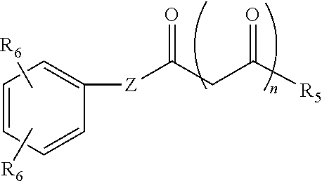
wherein R5 is C1-C6 alkyl, perhaloalkyl, or haloalkyl; Z is null or alkylene; n is 0 or 1; R6 is H, C1-C6 alkoxy, perhaloalkyl, or haloalkyl.

The incorporation of plasticizer into both the CTL, CGL, and the ground strip layer not only is successful to provide the benefits of providing the resulting imaging member belt with excellent curl suppression (eliminating the need for the ACBC), it also produces excellent photoelectrical property stability and prevents early onset of fatigue CTL cracking too to provide imaging member belt service life extension in the field.

where n is 270

wherein z represents the number of bisphenol A repeating units in segmental block (A) of from about 9 to about 18, y is number of repeating phthalic acid segmental block (B) of from about 1 to about 2, and n is the degree of polymerization between about 20 and about 90 for the copolymer having a weight average molecular weight between about 100,000 and about 250,000 and mixtures thereof.

Claims (15)


Priority Applications (1)
| Application Number | Priority Date | Filing Date | Title |
|---|---|---|---|
| US13/944,813 US9201318B2 (en) | 2013-07-17 | 2013-07-17 | Polymer for charge generation layer and charge transport layer formulation |
Applications Claiming Priority (1)
| Application Number | Priority Date | Filing Date | Title |
|---|---|---|---|
| US13/944,813 US9201318B2 (en) | 2013-07-17 | 2013-07-17 | Polymer for charge generation layer and charge transport layer formulation |
Publications (2)
| Publication Number | Publication Date |
|---|---|
| US20150024310A1 US20150024310A1 (en) | 2015-01-22 |
| US9201318B2 true US9201318B2 (en) | 2015-12-01 |
Family
ID=52343834
Family Applications (1)
| Application Number | Title | Priority Date | Filing Date |
|---|---|---|---|
| US13/944,813 Expired - Fee Related US9201318B2 (en) | 2013-07-17 | 2013-07-17 | Polymer for charge generation layer and charge transport layer formulation |
Country Status (1)
| Country | Link |
|---|---|
| US (1) | US9201318B2 (en) |
Cited By (1)
| Publication number | Priority date | Publication date | Assignee | Title |
|---|---|---|---|---|
| US20220215220A1 (en) * | 2019-04-19 | 2022-07-07 | Linxens Holding | Biometric Sensor Module for a Smart Card and Method for Manufacturing Such a Module |
Families Citing this family (1)
| Publication number | Priority date | Publication date | Assignee | Title |
|---|---|---|---|---|
| US9851647B1 (en) * | 2016-10-13 | 2017-12-26 | Xerox Corporation | Polycarbonate containing photoconductors |
Citations (29)
| Publication number | Priority date | Publication date | Assignee | Title |
|---|---|---|---|---|
| US3121006A (en) | 1957-06-26 | 1964-02-11 | Xerox Corp | Photo-active member for xerography |
| US4265990A (en) | 1977-05-04 | 1981-05-05 | Xerox Corporation | Imaging system with a diamine charge transport material in a polycarbonate resin |
| US4286033A (en) | 1980-03-05 | 1981-08-25 | Xerox Corporation | Trapping layer overcoated inorganic photoresponsive device |
| US4291110A (en) | 1979-06-11 | 1981-09-22 | Xerox Corporation | Siloxane hole trapping layer for overcoated photoreceptors |
| US4338387A (en) | 1981-03-02 | 1982-07-06 | Xerox Corporation | Overcoated photoreceptor containing inorganic electron trapping and hole trapping layers |
| US4664995A (en) | 1985-10-24 | 1987-05-12 | Xerox Corporation | Electrostatographic imaging members |
| US5069993A (en) | 1989-12-29 | 1991-12-03 | Xerox Corporation | Photoreceptor layers containing polydimethylsiloxane copolymers |
| US5153094A (en) | 1990-06-14 | 1992-10-06 | Xerox Corporation | Processes for the preparation of photogenerating pigments |
| US5166339A (en) | 1990-06-04 | 1992-11-24 | Xerox Corporation | Processes for the preparation of titanium phthalocyanines |
| US5189155A (en) | 1991-04-11 | 1993-02-23 | Xerox Corporation | Titanyl phthalocyanine Type I processes |
| US5189156A (en) | 1991-04-01 | 1993-02-23 | Xerox Corporation | Processes for the preparation of titanium-phthalocyanine Type X |
| US5215839A (en) | 1991-12-23 | 1993-06-01 | Xerox Corporation | Method and system for reducing surface reflections from an electrophotographic imaging member |
| US5382486A (en) | 1993-03-29 | 1995-01-17 | Xerox Corporation | Electrostatographic imaging member containing conductive polymer layers |
| US5660961A (en) | 1996-01-11 | 1997-08-26 | Xerox Corporation | Electrophotographic imaging member having enhanced layer adhesion and freedom from reflection interference |
| US5697024A (en) | 1996-01-11 | 1997-12-09 | Xerox Corporation | Differential increase in dark decay comparison |
| US5703487A (en) | 1996-01-11 | 1997-12-30 | Xerox Corporation | Detection of charge deficient spot susceptibility |
| US5756245A (en) | 1997-06-05 | 1998-05-26 | Xerox Corporation | Photoconductive imaging members |
| US5958638A (en) | 1997-06-23 | 1999-09-28 | Sharp Kabushiki Kaisha | Electrophotographic photoconductor and method of producing same |
| US6008653A (en) | 1997-10-30 | 1999-12-28 | Xerox Corporation | Contactless system for detecting microdefects on electrostatographic members |
| US6119536A (en) | 1997-10-30 | 2000-09-19 | Xerox Corporation | Constant distance contactless device |
| US6150824A (en) | 1997-10-30 | 2000-11-21 | Xerox Corporation | Contactless system for detecting subtle surface potential charge patterns |
| US6660441B2 (en) | 2002-01-07 | 2003-12-09 | Xerox Corporation | Simplified flexible electrostatographic imaging member belt |
| US7166399B2 (en) | 2004-04-14 | 2007-01-23 | Xerox Corporation | Photosensitive member having anti-curl backing layer with lignin sulfonic acid doped polyaniline |
| US20070054209A1 (en) * | 2005-09-07 | 2007-03-08 | Jun Azuma | Electrophotographic photoconductor |
| US7413835B2 (en) | 2005-07-14 | 2008-08-19 | Xerox Corporation | Imaging members |
| US7455941B2 (en) | 2005-12-21 | 2008-11-25 | Xerox Corporation | Imaging member with multilayer anti-curl back coating |
| US7462434B2 (en) | 2005-12-21 | 2008-12-09 | Xerox Corporation | Imaging member with low surface energy polymer in anti-curl back coating layer |
| US20110229808A1 (en) * | 2010-03-17 | 2011-09-22 | Xerox Corporation | Curl-free imaging members with a slippery surface |
| US20110305981A1 (en) * | 2010-06-10 | 2011-12-15 | Yu Robert C U | Imaging members having improved imaging layers |
-
2013
- 2013-07-17 US US13/944,813 patent/US9201318B2/en not_active Expired - Fee Related
Patent Citations (29)
| Publication number | Priority date | Publication date | Assignee | Title |
|---|---|---|---|---|
| US3121006A (en) | 1957-06-26 | 1964-02-11 | Xerox Corp | Photo-active member for xerography |
| US4265990A (en) | 1977-05-04 | 1981-05-05 | Xerox Corporation | Imaging system with a diamine charge transport material in a polycarbonate resin |
| US4291110A (en) | 1979-06-11 | 1981-09-22 | Xerox Corporation | Siloxane hole trapping layer for overcoated photoreceptors |
| US4286033A (en) | 1980-03-05 | 1981-08-25 | Xerox Corporation | Trapping layer overcoated inorganic photoresponsive device |
| US4338387A (en) | 1981-03-02 | 1982-07-06 | Xerox Corporation | Overcoated photoreceptor containing inorganic electron trapping and hole trapping layers |
| US4664995A (en) | 1985-10-24 | 1987-05-12 | Xerox Corporation | Electrostatographic imaging members |
| US5069993A (en) | 1989-12-29 | 1991-12-03 | Xerox Corporation | Photoreceptor layers containing polydimethylsiloxane copolymers |
| US5166339A (en) | 1990-06-04 | 1992-11-24 | Xerox Corporation | Processes for the preparation of titanium phthalocyanines |
| US5153094A (en) | 1990-06-14 | 1992-10-06 | Xerox Corporation | Processes for the preparation of photogenerating pigments |
| US5189156A (en) | 1991-04-01 | 1993-02-23 | Xerox Corporation | Processes for the preparation of titanium-phthalocyanine Type X |
| US5189155A (en) | 1991-04-11 | 1993-02-23 | Xerox Corporation | Titanyl phthalocyanine Type I processes |
| US5215839A (en) | 1991-12-23 | 1993-06-01 | Xerox Corporation | Method and system for reducing surface reflections from an electrophotographic imaging member |
| US5382486A (en) | 1993-03-29 | 1995-01-17 | Xerox Corporation | Electrostatographic imaging member containing conductive polymer layers |
| US5697024A (en) | 1996-01-11 | 1997-12-09 | Xerox Corporation | Differential increase in dark decay comparison |
| US5660961A (en) | 1996-01-11 | 1997-08-26 | Xerox Corporation | Electrophotographic imaging member having enhanced layer adhesion and freedom from reflection interference |
| US5703487A (en) | 1996-01-11 | 1997-12-30 | Xerox Corporation | Detection of charge deficient spot susceptibility |
| US5756245A (en) | 1997-06-05 | 1998-05-26 | Xerox Corporation | Photoconductive imaging members |
| US5958638A (en) | 1997-06-23 | 1999-09-28 | Sharp Kabushiki Kaisha | Electrophotographic photoconductor and method of producing same |
| US6150824A (en) | 1997-10-30 | 2000-11-21 | Xerox Corporation | Contactless system for detecting subtle surface potential charge patterns |
| US6119536A (en) | 1997-10-30 | 2000-09-19 | Xerox Corporation | Constant distance contactless device |
| US6008653A (en) | 1997-10-30 | 1999-12-28 | Xerox Corporation | Contactless system for detecting microdefects on electrostatographic members |
| US6660441B2 (en) | 2002-01-07 | 2003-12-09 | Xerox Corporation | Simplified flexible electrostatographic imaging member belt |
| US7166399B2 (en) | 2004-04-14 | 2007-01-23 | Xerox Corporation | Photosensitive member having anti-curl backing layer with lignin sulfonic acid doped polyaniline |
| US7413835B2 (en) | 2005-07-14 | 2008-08-19 | Xerox Corporation | Imaging members |
| US20070054209A1 (en) * | 2005-09-07 | 2007-03-08 | Jun Azuma | Electrophotographic photoconductor |
| US7455941B2 (en) | 2005-12-21 | 2008-11-25 | Xerox Corporation | Imaging member with multilayer anti-curl back coating |
| US7462434B2 (en) | 2005-12-21 | 2008-12-09 | Xerox Corporation | Imaging member with low surface energy polymer in anti-curl back coating layer |
| US20110229808A1 (en) * | 2010-03-17 | 2011-09-22 | Xerox Corporation | Curl-free imaging members with a slippery surface |
| US20110305981A1 (en) * | 2010-06-10 | 2011-12-15 | Yu Robert C U | Imaging members having improved imaging layers |
Non-Patent Citations (6)
| Title |
|---|
| Ferdinand Rodriguez, Principles of Polymer Systems, Taylor & Francis Publisher (1996), pp. 58-59. |
| Genhai G. Liang, Wayne, D. Cook, Henry J. Sautereau and Abbas Tcharkhtchi, Diallyl Orthophthalate as a Reactive Plasticer for Polycarbonate, European Polymer Journal 44 (2008), pp. 366-375. |
| Hye-Yeon Cha, et al., U.S. Appl. No. 12/216,151, filed Jun. 30, 2008, now abandoned. |
| Robert C.U. Yu, et al., U.S. Appl. No. 10/982,719, filed Nov. 5, 2004, now U.S. Patent No. 7,592,111, issued Sep. 22, 2009. |
| Robert C.U. Yu, et al., U.S. Appl. No. 12/762,257, filed Apr. 16, 2010, now U.S. Patent No. 8,343,700, issued Jan. 1, 2013. |
| Robert C.U. Yu, et al., U.S. Appl. No. 12/782,671, filed May 18, 2010, now U.S. Patent No. 8,404,413, issued Mar. 26, 2013. |
Cited By (2)
| Publication number | Priority date | Publication date | Assignee | Title |
|---|---|---|---|---|
| US20220215220A1 (en) * | 2019-04-19 | 2022-07-07 | Linxens Holding | Biometric Sensor Module for a Smart Card and Method for Manufacturing Such a Module |
| US11775794B2 (en) * | 2019-04-19 | 2023-10-03 | Linxens Holding | Biometric sensor module for a smart card and method for manufacturing such a module |
Also Published As
| Publication number | Publication date |
|---|---|
| US20150024310A1 (en) | 2015-01-22 |
Similar Documents
| Publication | Publication Date | Title |
|---|---|---|
| US8168356B2 (en) | Structurally simplified flexible imaging members | |
| US8470505B2 (en) | Imaging members having improved imaging layers | |
| US8232030B2 (en) | Curl-free imaging members with a slippery surface | |
| US20070059622A1 (en) | Mechanically robust imaging member overcoat | |
| EP2253998A1 (en) | Flexible imaging members having a plasticized imaging layer | |
| EP2028549A2 (en) | Imaging member | |
| US8124305B2 (en) | Flexible imaging members without anticurl layer | |
| EP2290450B1 (en) | Flexible imaging member belts | |
| US8541151B2 (en) | Imaging members having a novel slippery overcoat layer | |
| US9201318B2 (en) | Polymer for charge generation layer and charge transport layer formulation | |
| US20120219893A1 (en) | Electrically tunable and stable imaging members | |
| US8475983B2 (en) | Imaging members having a chemical resistive overcoat layer | |
| EP2290449B1 (en) | Flexible imaging member belts | |
| US8173341B2 (en) | Flexible imaging members without anticurl layer | |
| US8603710B2 (en) | Alternate anticurl back coating formulation | |
| US8404413B2 (en) | Flexible imaging members having stress-free imaging layer(s) | |
| US9017906B2 (en) | Imaging members having a cross-linked anticurl back coating | |
| US8614038B2 (en) | Plasticized anti-curl back coating for flexible imaging member | |
| US9017908B2 (en) | Photoelectrical stable imaging members | |
| US8835085B2 (en) | Low strain anti-curl back coating for flexible imaging members | |
| US9063447B2 (en) | Imaging members having a cross-linked anticurl back coating | |
| US9075327B2 (en) | Imaging members and methods for making the same | |
| US9017907B2 (en) | Flexible imaging members having externally plasticized imaging layer(s) | |
| US8877413B2 (en) | Flexible imaging members comprising improved ground strip | |
| US20130216266A1 (en) | Imaging members comprising fluoroketone |
Legal Events
| Date | Code | Title | Description |
|---|---|---|---|
| AS | Assignment |
Owner name: XEROX CORPORATION, CONNECTICUT Free format text: ASSIGNMENT OF ASSIGNORS INTEREST;ASSIGNORS:YU, ROBERT C.U., MR.;AVERY, STEPHEN T., MR.;KELLY, JIMMY E., MR.;AND OTHERS;REEL/FRAME:030820/0318 Effective date: 20130716 |
|
| FEPP | Fee payment procedure |
Free format text: PAYOR NUMBER ASSIGNED (ORIGINAL EVENT CODE: ASPN); ENTITY STATUS OF PATENT OWNER: LARGE ENTITY |
|
| STCF | Information on status: patent grant |
Free format text: PATENTED CASE |
|
| MAFP | Maintenance fee payment |
Free format text: PAYMENT OF MAINTENANCE FEE, 4TH YEAR, LARGE ENTITY (ORIGINAL EVENT CODE: M1551); ENTITY STATUS OF PATENT OWNER: LARGE ENTITY Year of fee payment: 4 |
|
| AS | Assignment |
Owner name: CITIBANK, N.A., AS AGENT, DELAWARE Free format text: SECURITY INTEREST;ASSIGNOR:XEROX CORPORATION;REEL/FRAME:062740/0214 Effective date: 20221107 |
|
| AS | Assignment |
Owner name: XEROX CORPORATION, CONNECTICUT Free format text: RELEASE OF SECURITY INTEREST IN PATENTS AT R/F 062740/0214;ASSIGNOR:CITIBANK, N.A., AS AGENT;REEL/FRAME:063694/0122 Effective date: 20230517 |
|
| AS | Assignment |
Owner name: CITIBANK, N.A., AS COLLATERAL AGENT, NEW YORK Free format text: SECURITY INTEREST;ASSIGNOR:XEROX CORPORATION;REEL/FRAME:064760/0389 Effective date: 20230621 |
|
| FEPP | Fee payment procedure |
Free format text: MAINTENANCE FEE REMINDER MAILED (ORIGINAL EVENT CODE: REM.); ENTITY STATUS OF PATENT OWNER: LARGE ENTITY |
|
| AS | Assignment |
Owner name: JEFFERIES FINANCE LLC, AS COLLATERAL AGENT, NEW YORK Free format text: SECURITY INTEREST;ASSIGNOR:XEROX CORPORATION;REEL/FRAME:065628/0019 Effective date: 20231117 |
|
| LAPS | Lapse for failure to pay maintenance fees |
Free format text: PATENT EXPIRED FOR FAILURE TO PAY MAINTENANCE FEES (ORIGINAL EVENT CODE: EXP.); ENTITY STATUS OF PATENT OWNER: LARGE ENTITY |
|
| STCH | Information on status: patent discontinuation |
Free format text: PATENT EXPIRED DUE TO NONPAYMENT OF MAINTENANCE FEES UNDER 37 CFR 1.362 |
|
| FP | Lapsed due to failure to pay maintenance fee |
Effective date: 20231201 |
|
| AS | Assignment |
Owner name: CITIBANK, N.A., AS COLLATERAL AGENT, NEW YORK Free format text: SECURITY INTEREST;ASSIGNOR:XEROX CORPORATION;REEL/FRAME:066741/0001 Effective date: 20240206 |