US9207501B2 - Electrophoretic display panel and manufacturing method thereof - Google Patents
Electrophoretic display panel and manufacturing method thereof Download PDFInfo
- Publication number
- US9207501B2 US9207501B2 US14/454,716 US201414454716A US9207501B2 US 9207501 B2 US9207501 B2 US 9207501B2 US 201414454716 A US201414454716 A US 201414454716A US 9207501 B2 US9207501 B2 US 9207501B2
- Authority
- US
- United States
- Prior art keywords
- base material
- conductive lines
- electrode patterns
- electrophoretic display
- driving electrode
- Prior art date
- Legal status (The legal status is an assumption and is not a legal conclusion. Google has not performed a legal analysis and makes no representation as to the accuracy of the status listed.)
- Active
Links
Images


Classifications
-
- G—PHYSICS
- G02—OPTICS
- G02F—OPTICAL DEVICES OR ARRANGEMENTS FOR THE CONTROL OF LIGHT BY MODIFICATION OF THE OPTICAL PROPERTIES OF THE MEDIA OF THE ELEMENTS INVOLVED THEREIN; NON-LINEAR OPTICS; FREQUENCY-CHANGING OF LIGHT; OPTICAL LOGIC ELEMENTS; OPTICAL ANALOGUE/DIGITAL CONVERTERS
- G02F1/00—Devices or arrangements for the control of the intensity, colour, phase, polarisation or direction of light arriving from an independent light source, e.g. switching, gating or modulating; Non-linear optics
- G02F1/01—Devices or arrangements for the control of the intensity, colour, phase, polarisation or direction of light arriving from an independent light source, e.g. switching, gating or modulating; Non-linear optics for the control of the intensity, phase, polarisation or colour
- G02F1/13—Devices or arrangements for the control of the intensity, colour, phase, polarisation or direction of light arriving from an independent light source, e.g. switching, gating or modulating; Non-linear optics for the control of the intensity, phase, polarisation or colour based on liquid crystals, e.g. single liquid crystal display cells
- G02F1/133—Constructional arrangements; Operation of liquid crystal cells; Circuit arrangements
- G02F1/1333—Constructional arrangements; Manufacturing methods
- G02F1/1343—Electrodes
- G02F1/134309—Electrodes characterised by their geometrical arrangement
-
- G—PHYSICS
- G02—OPTICS
- G02F—OPTICAL DEVICES OR ARRANGEMENTS FOR THE CONTROL OF LIGHT BY MODIFICATION OF THE OPTICAL PROPERTIES OF THE MEDIA OF THE ELEMENTS INVOLVED THEREIN; NON-LINEAR OPTICS; FREQUENCY-CHANGING OF LIGHT; OPTICAL LOGIC ELEMENTS; OPTICAL ANALOGUE/DIGITAL CONVERTERS
- G02F1/00—Devices or arrangements for the control of the intensity, colour, phase, polarisation or direction of light arriving from an independent light source, e.g. switching, gating or modulating; Non-linear optics
- G02F1/01—Devices or arrangements for the control of the intensity, colour, phase, polarisation or direction of light arriving from an independent light source, e.g. switching, gating or modulating; Non-linear optics for the control of the intensity, phase, polarisation or colour
- G02F1/165—Devices or arrangements for the control of the intensity, colour, phase, polarisation or direction of light arriving from an independent light source, e.g. switching, gating or modulating; Non-linear optics for the control of the intensity, phase, polarisation or colour based on translational movement of particles in a fluid under the influence of an applied field
- G02F1/166—Devices or arrangements for the control of the intensity, colour, phase, polarisation or direction of light arriving from an independent light source, e.g. switching, gating or modulating; Non-linear optics for the control of the intensity, phase, polarisation or colour based on translational movement of particles in a fluid under the influence of an applied field characterised by the electro-optical or magneto-optical effect
- G02F1/167—Devices or arrangements for the control of the intensity, colour, phase, polarisation or direction of light arriving from an independent light source, e.g. switching, gating or modulating; Non-linear optics for the control of the intensity, phase, polarisation or colour based on translational movement of particles in a fluid under the influence of an applied field characterised by the electro-optical or magneto-optical effect by electrophoresis
-
- G—PHYSICS
- G02—OPTICS
- G02F—OPTICAL DEVICES OR ARRANGEMENTS FOR THE CONTROL OF LIGHT BY MODIFICATION OF THE OPTICAL PROPERTIES OF THE MEDIA OF THE ELEMENTS INVOLVED THEREIN; NON-LINEAR OPTICS; FREQUENCY-CHANGING OF LIGHT; OPTICAL LOGIC ELEMENTS; OPTICAL ANALOGUE/DIGITAL CONVERTERS
- G02F1/00—Devices or arrangements for the control of the intensity, colour, phase, polarisation or direction of light arriving from an independent light source, e.g. switching, gating or modulating; Non-linear optics
- G02F1/01—Devices or arrangements for the control of the intensity, colour, phase, polarisation or direction of light arriving from an independent light source, e.g. switching, gating or modulating; Non-linear optics for the control of the intensity, phase, polarisation or colour
- G02F1/165—Devices or arrangements for the control of the intensity, colour, phase, polarisation or direction of light arriving from an independent light source, e.g. switching, gating or modulating; Non-linear optics for the control of the intensity, phase, polarisation or colour based on translational movement of particles in a fluid under the influence of an applied field
- G02F1/1675—Constructional details
- G02F1/1676—Electrodes
-
- G02F2001/1676—
Definitions
- the invention relates to a display panel and a manufacturing method thereof, and more particularly to an electrophoretic display panel and a manufacturing method thereof.
- a normal electrophoretic display panel includes a driving substrate and an electrophoretic display substrate.
- the electrophoretic display substrate has an electrophoretic display material that includes a display solution and a plurality of display particles distributed into the display solution.
- the driving substrate drives the display particles
- the display particles are moved in an upward direction (i.e., approaching a user) or in a downward direction (moving away from the user).
- the display particles reflect an external light source, the user is able to observe the display particles or the color of the display solution, so as to watch a corresponding display image.
- numerous conductive lines are configured on the driving substrate, and the line width of the conductive lines is visible to human eyes, thus posing a negative impact on the resolution of the electrophoretic display panel.
- the invention is directed to an electrophoretic display panel which has a shielding layer capable of shielding conductive lines, and the electrophoretic display panel features favorable resolution.
- the invention is further directed to a manufacturing method of an electrophoretic display panel for forming the aforesaid electrophoretic display panel.
- an electrophoretic display panel that includes a driving substrate and an electrophoretic display substrate.
- the driving substrate includes a first base material, a plurality of driving electrode patterns, a plurality of conductive lines, and a shielding layer.
- the first base material has a first configuration region and a second configuration region surrounding the first configuration region.
- the driving electrode patterns are disposed on the first base material and located in the first configuration region.
- the conductive lines are disposed on the first base material.
- the conductive lines are respectively connected to the driving electrode patterns and respectively extend from the first configuration region to the second configuration region.
- the shielding layer is disposed on the first base material.
- the shielding layer shields the conductive lines and exposes the driving electrode patterns.
- the electrophoretic display substrate is disposed above the driving substrate.
- the electrophoretic display substrate includes a second base material, an electrode layer, and a plurality of display media.
- the second base material is located opposite to the first base material.
- the electrode layer is disposed on the second base material and located between the first and second base materials.
- the display media are disposed between the electrode layer and the driving electrode patterns.
- a material of the shielding layer includes a photoresist material or an insulating material.
- the shielding layer has a plurality of openings. Each of the openings respectively exposes a portion of the conductive lines.
- the driving electrode patterns are located on the shielding layer and electrically connected to the portions of the conductive lines exposed by the openings through the openings.
- each of the display media includes an electrophoretic liquid, a plurality of black charged particles, and a plurality of white charged particles, and the black charged particles and the white charged particles are distributed into the electrophoretic liquid.
- the electrophoretic display panel further includes an adhesive layer disposed between the driving substrate and the electrophoretic display substrate, and the electrophoretic display substrate is fixed to the driving substrate through the adhesive layer.
- a manufacturing method of an electrophoretic display panel includes following steps.
- a first base material is provided.
- the first base material has a first configuration region and a second configuration region surrounding the first configuration region.
- a plurality of driving electrode patterns are formed in the first configuration region, and a plurality of conductive lines extending from the first configuration region to the second configuration region are formed on the first base material.
- a photoresist layer is formed on the first base material. The photoresist layer covers the driving electrode patterns, the conductive lines, and a portion of the first base material.
- An exposure and development process is preformed on the photoresist layer to form a shielding layer shielding the conductive lines, and the first base material, the driving electrode patterns, the conductive lines, and the shielding layer together constitute a driving substrate.
- An electrophoretic display substrate is adhered onto the driving substrate, and the electrophoretic display substrate includes a second base material, an electrode layer, and a plurality of display media.
- the second base material is located opposite to the first base material.
- the electrode layer is disposed on the second base material and located between the first and second base materials.
- the display media are at least disposed between the electrode layer and the driving electrode patterns.
- the step of forming the driving electrode patterns and the conductive lines includes the following.
- a conductive material layer is formed in the first configuration region and the second configuration region of the first base material.
- a first photoresist layer is formed on the conductive material layer, and the first photoresist layer covers the conductive material layer.
- a first exposure and development process is performed on the first photoresist layer to form a first patterned photoresist layer.
- a portion of the conductive material layer exposed by the first patterned photoresist layer is etched with use of the first patterned photoresist layer as an etching mask, so as to form the driving electrode patterns located in the first configuration region and the conductive lines respectively extending from the first configuration region to the second configuration region.
- the first patterned photoresist layer is removed to expose the driving electrode patterns, the conductive lines, and the portion of the first base material.
- a material of the shielding layer includes a photoresist material.
- the manufacturing method of the electrophoretic display panel further includes following steps. Before the photoresist layer is formed on the first base material, an insulating material layer is formed to cover the driving electrode patterns, the conductive lines, and the portion of the first base material. An exposure and development process is performed on the photoresist layer to form a patterned photoresist layer. A portion of the insulating material layer exposed by the patterned photoresist layer is etched with use of the patterned photoresist layer as an etching mask, so as to form the shielding layer. Before the electrophoretic display substrate is adhered onto the driving substrate, the patterned photoresist layer is removed.
- a material of the shielding layer includes an insulating material.
- a material of the photoresist layer includes positive-type photoresist or negative-type photoresist.
- each of the display media includes an electrophoretic liquid, a plurality of black charged particles, and a plurality of white charged particles, and the black charged particles and the white charged particles are distributed into the electrophoretic liquid.
- a manufacturing method of an electrophoretic display panel includes following steps.
- a first base material having a first configuration region and a second configuration region surrounding the first configuration region is provided.
- a plurality of conductive lines extending from the first configuration region to the second configuration region is formed on the first base material.
- a shielding layer is formed on the first base material.
- the shielding layer covers the first and second configuration regions of the first base material and has a plurality of openings. Each of the openings respectively exposes a portion of the conductive lines.
- a plurality of driving electrode patterns is formed on the shielding layer.
- the driving electrode patterns are disposed in the first configuration region and respectively connected to the portion of the conductive lines exposed by the openings through the openings.
- the first base material, the driving electrode patterns, the conductive lines, and the shielding layer together constitute a driving substrate.
- An electrophoretic display substrate is adhered onto the driving substrate, and the electrophoretic display substrate includes a second base material, an electrode layer, and a plurality of display media.
- the second base material is disposed opposite to the first base material
- the electrode layer is disposed on the second base material and located between the second base material and the first base material
- the display media is at least disposed between the electrode layer and the driving electrode patterns.
- a method of aiming the shielding layer includes performing a photoresist coating process, an exposure and development process, and an etching process.
- a method of forming the driving electrode patterns includes performing a photoresist coating process, an exposure and development process, and an etching process.
- a method of forming the conductive lines includes performing a photoresist coating process, an exposure and development process, and an etching process.
- each of the display media includes an electrophoretic liquid, a plurality of black charged particles, and a plurality of white charged particles, and the black charged particles and the white charged particles are distributed into the electrophoretic liquid.
- the shielding layer in the electrophoretic display panel as described in the embodiments of the invention is formed by performing the exposure and development process, so as to effectively shield the conductive lines and prevent the conductive lines from being observed by human eyes. As such, the resolution of the electrophoretic display panel may be effectively ameliorated.
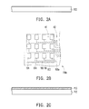
- FIG. 1A is a schematic cross-sectional view illustrating an electrophoretic display panel according to an embodiment of the invention.
- FIG. 1B is a schematic top view illustrating a driving substrate depicted in FIG. 1A .
- FIG. 2A through FIG. 2K are schematic views illustrating a manufacturing method of an electrophoretic display panel according to an embodiment of the invention.
- FIG. 3A through FIG. 3G are cross-sectional views illustrating a manufacturing method of an electrophoretic display panel according to another embodiment of the invention.
- FIG. 4A through FIG. 4D are cross-sectional views illustrating a manufacturing method of an electrophoretic display panel according to still another embodiment of the invention.
- FIG. 1A is a schematic cross-sectional view illustrating an electrophoretic display panel according to an embodiment of the invention.
- FIG. 1B is a schematic top view illustrating a driving substrate depicted in FIG. 1A .
- the electrophoretic display panel 100 a in the present embodiment includes a driving substrate 110 a and an electrophoretic display substrate 120 .
- the driving substrate 110 a includes a first base material 112 , a plurality of driving electrode patterns 114 , a plurality of conductive lines 116 , and a shielding layer 118 a .
- the first base material 112 has a first configuration region A 1 and a second configuration region A 2 surrounding the first configuration region A 1 .
- the driving electrode patterns 114 are disposed on the first base material 112 and located in the first configuration region A 1 .
- the conductive lines 116 are disposed on the first base material 112 and respectively connected to the driving electrode patterns 114 .
- the conductive lines 116 respectively extend from the first configuration region A 1 to the second configuration region A 2 .
- the shielding layer 118 a is disposed on the first base material 112 .
- the shielding layer 118 a shields the conductive lines 116 and exposes the driving electrode patterns 114 .
- the shielding layer 118 a is made of a photoresist material or an insulating material, for instance.
- the electrophoretic display substrate 120 is disposed above the driving substrate 110 a .
- the electrophoretic display substrate 120 includes a second base material 122 , an electrode layer 124 , and a plurality of display media 126 .
- the second base material 122 is located opposite to the first base material 112 .
- the electrode layer 124 is disposed on the second base material 122 and located between the first base material 112 and the second base material 112 and 122 .
- the display media 126 are disposed between the electrode layer 124 and the driving electrode patterns 114 .
- the first configuration region A 1 where the driving electrode patterns 114 are located may be considered a display region
- the second configuration region A 2 where no driving electrode pattern 114 is located may be considered a non-display region.
- Each of the display media 126 includes an electrophoretic liquid 127 , a plurality of black charged particles 128 , and a plurality of white charged particles 129 , and the black charged particles 128 and the white charged particles 129 are distributed into the electrophoretic liquid 127 .
- the electrophoretic display panel 100 a further includes an adhesive layer 130 disposed between the driving substrate 110 a and the electrophoretic display substrate 120 , and the electrophoretic display substrate 120 is fixed to the driving substrate 110 a through the adhesive layer 130 .
- the electrophoretic display panel 100 a described in the present embodiment has the shielding layer 118 a that shields the conductive lines 116 , the conductive lines 116 are invisible to human eyes, and the resolution of the electrophoretic display panel 100 a may be effectively ameliorated.
- the structure of the electrophoretic display panel 100 a is provided above, while the manufacturing process of the electrophoretic display panel 100 a is not introduced yet.
- the manufacturing process of electrophoretic display panels 100 a , 100 b , and 100 c are respectively elaborated in the following three embodiments.
- FIG. 2A through FIG. 2K are schematic views illustrating a manufacturing method of an electrophoretic display panel according to an embodiment of the invention.
- FIG. 2B is a top view schematically illustrating the driving substrate
- FIG. 2A and FIG. 2C to FIG. 2K are cross-sectional views schematically illustrating the manufacturing method of the electrophoretic display panel.
- a first base material 112 is provided in the manufacturing method of the electrophoretic display panel 100 a described in the present embodiment.
- the first base material 112 has a first configuration region A 1 and a second configuration region A 2 surrounding the first configuration region A 1 .
- a conductive material layer 113 is formed in the first configuration region A 1 and the second configuration region A 2 , and the conductive material layer 113 covers the first base material 112 .
- the conductive material layer 113 is made of metal or a transparent conductive material, for instance.
- a first photoresist layer 115 is formed on the conductive material layer 113 , and the first photoresist layer 115 covers the conductive material layer 113 .
- the first photoresist layer 115 is made of negative-type photoresist.
- the first photoresist layer 115 is likely to be made of positive-type photoresist.
- a first exposure and development process is performed on the first photoresist layer 115 with use of a photomask M 1 , so as to form a first patterned photoresist layer 115 a.
- a portion of the conductive material layer 113 exposed by the first patterned photoresist layer 115 a is etched with use of the first patterned photoresist layer 115 a as an etching mask, so as to form the driving electrode patterns 114 and the conductive lines 116 .
- the driving electrode patterns 114 are located in the first configuration region A 1
- the conductive lines 116 are respectively connected to the driving electrode patterns 114 and respectively extend from the first configuration region A 1 to the second configuration region A 2 .
- the first patterned photoresist layer 115 a is removed to expose the driving electrode patterns 114 , the conductive lines 116 , and the portion of the first base material 112 .
- a second photoresist layer 117 is formed on the first base material 112 , and the second photoresist layer 117 covers the driving electrode patterns 114 , the conductive lines 116 , and the portion of the first base material 112 .
- the second photoresist layer 117 is made of positive-type photoresist.
- the second photoresist layer 117 is likely to be made of negative-type photoresist.
- a second exposure and development process is performed on the second photoresist layer 117 with use of a photomask M 2 , so as to form a shielding layer 118 a that shields the conductive lines 116 .
- the shielding layer 118 a shields the conductive lines 116 and exposes the driving electrode patterns 114 .
- the shielding layer 118 a is made of a photoresist material. Namely, the shielding layer 118 a is the patterned second photoresist layer 117 .
- the first base material 112 , the driving electrode patterns 114 , the conductive lines 116 , and the shielding layer 118 a together constitute a driving substrate 110 a.
- an electrophoretic display substrate 120 is adhered to the driving substrate 110 a through an adhesive layer 130 .
- the electrophoretic display substrate 120 includes a second base material 122 , an electrode layer 124 , and a plurality of display media 126 .
- the second base material 122 is located opposite to the first base material 112 .
- the electrode layer 124 is disposed on the second base material 122 and located between the first base material 112 and the second base material 122 .
- the display media 126 are at least disposed between the electrode layer 124 and the driving electrode patterns 114 .
- Each of the display media 126 includes an electrophoretic liquid 127 , a plurality of black charged particles 128 , and a plurality of white charged particles 129 , and the black charged particles 128 and the white charged particles 129 are distributed into the electrophoretic liquid 127 . So far, the electrophoretic display panel 100 a is completely formed.
- the driving electrode patterns 114 and the conductive lines 116 in the electrophoretic display panel 100 a of the present embodiment are formed by performing a first photoresist coating process (i.e., forming the first photoresist layer 115 ), an exposure and development process, and an etching process, the line width of the conductive lines 116 may be effectively reduced.
- a second photoresist coating process i.e., forming the second photoresist layer 117
- another exposure and development process are then performed to form the shielding layer 118 a that shields the conductive lines 116 .
- the conductive lines 116 may be effectively shielded by the shielding layer 118 a and are not visible to human eyes.
- the resolution of the electrophoretic display panel 100 a may be enhanced.
- FIG. 3A through FIG. 3G are cross-sectional views illustrating a manufacturing method of an electrophoretic display panel according to another embodiment of the invention.
- the electrophoretic display panel 100 b of the present embodiment is similar to the electrophoretic display panel 100 a depicted in FIG. 1A .
- the main difference lies in that the material of the shielding layer 118 b in the present embodiment is different from the material of the shielding layer 118 a in the previous embodiment.
- the electrophoretic display panel 100 b of the present embodiment may be formed by performing the steps of forming the electrophoretic display panel 100 a of the previous embodiment. Besides, after the step shown in FIG. 2G is carried out, the first patterned photoresist layer 115 a is removed, so as to expose the driving electrode patterns 114 , the conductive lines 116 , and the portion of the first base material 112 . As indicated in FIG. 3A , an insulating material layer 119 is formed to cover the driving electrode patterns 114 , the conductive lines 116 , and the portion of the first base material 112 .
- a second photoresist layer 117 a is formed on the first substrate 112 , and the second photoresist layer 117 a covers the insulating material layer 119 .
- the second photoresist layer 117 a is made of positive-type photoresist.
- the second photoresist layer 117 a is likely to be made of negative-type photoresist.
- a second photolithography process is performed on the second photoresist layer 117 a with use of a photomask M 3 , so as to form a second patterned photoresist layer 117 b.
- a portion of the insulating material layer 119 exposed by the second patterned photoresist layer 117 b is etched with use of the second patterned photoresist layer 117 b as an etching mask, so as to form a shielding layer 118 b .
- the shielding layer 118 b is made of an insulating material. Namely, the shielding layer 118 b is the patterned insulating material layer 119 .
- the second patterned photoresist layer 117 b is removed to expose the driving electrode patterns 114 , the conductive lines 116 , the shielding layer 118 b , and the portion of the first base material 112 .
- the first base material 112 , the driving electrode patterns 114 , the conductive lines 116 , and the shielding layer 118 b together constitute a driving substrate 110 b .
- the shielding layer 118 b shields the conductive lines 116 and exposes the driving electrode patterns 114 .
- an electrophoretic display substrate 120 is adhered to the driving substrate 110 b through an adhesive layer 130 .
- the electrophoretic display substrate 120 includes a second base material 122 , an electrode layer 124 , and a plurality of display media 126 .
- the second base material 122 is located opposite to the first base material 112 .
- the electrode layer 124 is disposed on the second base material 122 and located between the first base materials 112 and the second base materials 122 .
- the display media 126 are at least disposed between the electrode layer 124 and the driving electrode patterns 114 .
- Each of the display media 126 includes an electrophoretic liquid 127 , a plurality of black charged particles 128 , and a plurality of white charged particles 129 , and the black charged particles 128 and the white charged particles 129 are distributed into the electrophoretic liquid 127 . So far, the electrophoretic display panel 100 b is completely formed.
- FIG. 4A through FIG. 4D are cross-sectional views illustrating a manufacturing method of an electrophoretic display panel according to still another embodiment of the invention.
- the electrophoretic display panel 100 c of the present embodiment is similar to the electrophoretic display panel 100 a depicted in FIG. 1A .
- the main difference lies in that the material of the shielding layer 118 c in the present embodiment is different from the material of the shielding layer 118 a in the previous embodiment, and that the arrangement of the driving electrode patterns 114 c , the conductive lines 116 c , and the shielding layer 118 c is different from the arrangement of the driving electrode patterns 114 , the conductive lines 116 , and the shielding layer 118 a.
- a first base material 112 c is provided, and the first base material 112 c has a plurality of conductive lines 116 c formed thereon.
- the conductive lines 116 c are formed by performing a photoresist coating process, an exposure and development process, and an etching process, and the steps of forming the conductive lines 116 c are similar to the steps of forming the driving electrode patterns 114 and the conductive lines 116 shown in FIG. 2A to FIG. 2G . Therefore, no further description is provided hereinafter.
- the location where the conductive lines 116 c are configured is the same as the location where the conductive lines 116 are configured, i.e., the conductive lines 116 c also extend from the first configuration region A 1 (shown in FIG. 2B ) to the second configuration region A 2 (shown in FIG. 2B ).
- a shielding layer 118 c is formed on the conductive lines 116 c and the first base material 112 c , and the shielding layer 118 c shields the conductive lines 116 c and has a plurality of openings C. Each of the openings C respectively exposes a portion of the conductive lines 116 c .
- the shielding layer 118 c for instance, is formed by performing a photoresist coating process, an exposure and development process, and an etching process, and the steps of forming the shielding layer 118 c are similar to the steps of forming the driving electrode patterns 114 , the conductive lines 116 , or the shielding layer 118 b shown in FIG. 3A to FIG. 3F . Therefore, no further description is provided hereinafter.
- a plurality of driving electrode patterns 114 c are formed on the shielding layer 118 c .
- the driving electrode patterns 114 c are respectively connected to the portion of the conductive lines 116 c respectively exposed by the openings C through the openings C.
- the shielding layer 118 c shields the conductive lines 116 c and exposes the driving electrode patterns 114 c .
- the driving electrode patterns 114 c are formed by performing a photoresist coating process, an exposure and development process, and an etching process, and the steps of forming the driving electrode patterns 114 c are similar to the steps of forming the driving electrode patterns 114 and the conductive lines 116 shown in FIG. 2A to FIG. 2G .
- the location where the driving electrode patterns 114 c are configured is the same as the location where the driving electrode patterns 114 are configured, i.e., the driving electrode patterns 114 c are also disposed in the first configuration region A 1 (shown in FIG. 2B ).
- the first base material 112 c , the driving electrode patterns 114 c , the conductive lines 116 c , and the shielding layer 118 c together constitute a driving substrate 110 c.
- an electrophoretic display substrate 120 is adhered to the driving substrate 110 c through an adhesive layer 130 .
- the electrophoretic display substrate 120 includes a second base material 122 , an electrode layer 124 , and a plurality of display media 126 .
- the second base material 122 is located opposite to the first base material 112 c .
- the electrode layer 124 is disposed on the second base material 122 and located between the first base material 112 c and the second base material 122 .
- the display media 126 are at least disposed between the electrode layer 124 and the driving electrode patterns 114 c .
- Each of the display media 126 includes an electrophoretic liquid 127 , a plurality of black charged particles 128 , and a plurality of white charged particles 129 , and the black charged particles 128 and the white charged particles 129 are distributed into the electrophoretic liquid 127 . So far, the electrophoretic display panel 100 c is completely formed.
- the driving electrode patterns and the conductive lines in the electrophoretic display panel described in the embodiments of the invention are formed by performing a photoresist coating process (i.e., forming the first photoresist layer), an exposure and development process, and an etching process, and thus the line width of the conductive lines may be effectively reduced.
- a second photoresist coating process i.e., forming the second photoresist layer
- another exposure and development process are then performed to form the shielding layer that shields the conductive lines.
- the conductive lines may be effectively shielded by the shielding layer and are not visible to human eyes.
- the resolution of the electrophoretic display panel may be enhanced.
Abstract
An electrophoretic display panel includes a driving substrate and an electrophoretic display substrate. The driving substrate includes a first base material, driving electrode patterns, conductive lines, and a shielding layer. The first base material has a first configuration region and a second configuration region. The driving electrode patterns are located inside the first configuration region. The conductive lines are respectively connected to the driving electrode patterns and respectively extend from the first configuration region to the second configuration region. The shielding layer shields the conductive lines and exposes the driving electrode patterns. The electrophoretic display substrate includes a second base material located opposite to the first base material, an electrode layer, and display media. The electrode layer is disposed on the second base material and between the first and second base materials. The display media are disposed between the electrode layer and the driving electrode patterns.
Description
This application is a divisional of an application Ser. No. 13/466,145 filed on May 8, 2012, now pending, which claims the priority benefit of Taiwan application serial no. 101108148, filed on Mar. 9, 2012. The entirety of the above-mentioned patent application is hereby incorporated by reference herein and made a part of specification.
1. Field of the Invention
The invention relates to a display panel and a manufacturing method thereof, and more particularly to an electrophoretic display panel and a manufacturing method thereof.
2. Description of Related Art
With the widespread use of information products and development of science and technology, manufacturers continuously aim at characterizing displays by light weight, compactness, and flexibility. Among the displays, an electrophoretic display has attracted great attention.
A normal electrophoretic display panel includes a driving substrate and an electrophoretic display substrate. The electrophoretic display substrate has an electrophoretic display material that includes a display solution and a plurality of display particles distributed into the display solution. When the driving substrate drives the display particles, the display particles are moved in an upward direction (i.e., approaching a user) or in a downward direction (moving away from the user). After the display particles reflect an external light source, the user is able to observe the display particles or the color of the display solution, so as to watch a corresponding display image. Nonetheless, numerous conductive lines are configured on the driving substrate, and the line width of the conductive lines is visible to human eyes, thus posing a negative impact on the resolution of the electrophoretic display panel.
The invention is directed to an electrophoretic display panel which has a shielding layer capable of shielding conductive lines, and the electrophoretic display panel features favorable resolution.
The invention is further directed to a manufacturing method of an electrophoretic display panel for forming the aforesaid electrophoretic display panel.
In the invention, an electrophoretic display panel that includes a driving substrate and an electrophoretic display substrate is provided. The driving substrate includes a first base material, a plurality of driving electrode patterns, a plurality of conductive lines, and a shielding layer. The first base material has a first configuration region and a second configuration region surrounding the first configuration region. The driving electrode patterns are disposed on the first base material and located in the first configuration region. The conductive lines are disposed on the first base material. Here, the conductive lines are respectively connected to the driving electrode patterns and respectively extend from the first configuration region to the second configuration region. The shielding layer is disposed on the first base material. Here, the shielding layer shields the conductive lines and exposes the driving electrode patterns. The electrophoretic display substrate is disposed above the driving substrate. Besides, the electrophoretic display substrate includes a second base material, an electrode layer, and a plurality of display media. The second base material is located opposite to the first base material. The electrode layer is disposed on the second base material and located between the first and second base materials. The display media are disposed between the electrode layer and the driving electrode patterns.
According to an embodiment of the invention, a material of the shielding layer includes a photoresist material or an insulating material.
According to an embodiment of the invention, the shielding layer has a plurality of openings. Each of the openings respectively exposes a portion of the conductive lines. The driving electrode patterns are located on the shielding layer and electrically connected to the portions of the conductive lines exposed by the openings through the openings.
According to an embodiment of the invention, each of the display media includes an electrophoretic liquid, a plurality of black charged particles, and a plurality of white charged particles, and the black charged particles and the white charged particles are distributed into the electrophoretic liquid.
According to an embodiment of the invention, the electrophoretic display panel further includes an adhesive layer disposed between the driving substrate and the electrophoretic display substrate, and the electrophoretic display substrate is fixed to the driving substrate through the adhesive layer.
In the invention, a manufacturing method of an electrophoretic display panel includes following steps. A first base material is provided. Here, the first base material has a first configuration region and a second configuration region surrounding the first configuration region. A plurality of driving electrode patterns are formed in the first configuration region, and a plurality of conductive lines extending from the first configuration region to the second configuration region are formed on the first base material. A photoresist layer is formed on the first base material. The photoresist layer covers the driving electrode patterns, the conductive lines, and a portion of the first base material. An exposure and development process is preformed on the photoresist layer to form a shielding layer shielding the conductive lines, and the first base material, the driving electrode patterns, the conductive lines, and the shielding layer together constitute a driving substrate. An electrophoretic display substrate is adhered onto the driving substrate, and the electrophoretic display substrate includes a second base material, an electrode layer, and a plurality of display media. The second base material is located opposite to the first base material. The electrode layer is disposed on the second base material and located between the first and second base materials. The display media are at least disposed between the electrode layer and the driving electrode patterns.
According to an embodiment of the invention, the step of forming the driving electrode patterns and the conductive lines includes the following. A conductive material layer is formed in the first configuration region and the second configuration region of the first base material. A first photoresist layer is formed on the conductive material layer, and the first photoresist layer covers the conductive material layer. A first exposure and development process is performed on the first photoresist layer to form a first patterned photoresist layer. A portion of the conductive material layer exposed by the first patterned photoresist layer is etched with use of the first patterned photoresist layer as an etching mask, so as to form the driving electrode patterns located in the first configuration region and the conductive lines respectively extending from the first configuration region to the second configuration region. The first patterned photoresist layer is removed to expose the driving electrode patterns, the conductive lines, and the portion of the first base material.
According to an embodiment of the invention, a material of the shielding layer includes a photoresist material.
According to an embodiment of the invention, the manufacturing method of the electrophoretic display panel further includes following steps. Before the photoresist layer is formed on the first base material, an insulating material layer is formed to cover the driving electrode patterns, the conductive lines, and the portion of the first base material. An exposure and development process is performed on the photoresist layer to form a patterned photoresist layer. A portion of the insulating material layer exposed by the patterned photoresist layer is etched with use of the patterned photoresist layer as an etching mask, so as to form the shielding layer. Before the electrophoretic display substrate is adhered onto the driving substrate, the patterned photoresist layer is removed.
According to an embodiment of the invention, a material of the shielding layer includes an insulating material.
According to an embodiment of the invention, a material of the photoresist layer includes positive-type photoresist or negative-type photoresist.
According to an embodiment of the invention, each of the display media includes an electrophoretic liquid, a plurality of black charged particles, and a plurality of white charged particles, and the black charged particles and the white charged particles are distributed into the electrophoretic liquid.
In the invention, a manufacturing method of an electrophoretic display panel includes following steps. A first base material having a first configuration region and a second configuration region surrounding the first configuration region is provided. A plurality of conductive lines extending from the first configuration region to the second configuration region is formed on the first base material. A shielding layer is formed on the first base material. Here, the shielding layer covers the first and second configuration regions of the first base material and has a plurality of openings. Each of the openings respectively exposes a portion of the conductive lines. A plurality of driving electrode patterns is formed on the shielding layer. Here, the driving electrode patterns are disposed in the first configuration region and respectively connected to the portion of the conductive lines exposed by the openings through the openings. The first base material, the driving electrode patterns, the conductive lines, and the shielding layer together constitute a driving substrate. An electrophoretic display substrate is adhered onto the driving substrate, and the electrophoretic display substrate includes a second base material, an electrode layer, and a plurality of display media. The second base material is disposed opposite to the first base material, the electrode layer is disposed on the second base material and located between the second base material and the first base material, and the display media is at least disposed between the electrode layer and the driving electrode patterns.
According to an embodiment of the invention, a method of aiming the shielding layer includes performing a photoresist coating process, an exposure and development process, and an etching process.
According to an embodiment of the invention, a method of forming the driving electrode patterns includes performing a photoresist coating process, an exposure and development process, and an etching process.
According to an embodiment of the invention, a method of forming the conductive lines includes performing a photoresist coating process, an exposure and development process, and an etching process.
According to an embodiment of the invention, each of the display media includes an electrophoretic liquid, a plurality of black charged particles, and a plurality of white charged particles, and the black charged particles and the white charged particles are distributed into the electrophoretic liquid.
Based on the above, the shielding layer in the electrophoretic display panel as described in the embodiments of the invention is formed by performing the exposure and development process, so as to effectively shield the conductive lines and prevent the conductive lines from being observed by human eyes. As such, the resolution of the electrophoretic display panel may be effectively ameliorated.
Other features and advantages of the invention will be further understood from the further technological features disclosed by the embodiments of the invention wherein there are shown and described embodiments of this invention, simply by way of illustration of modes best suited to carry out the invention.
The accompanying drawings are included to provide further understanding, and are incorporated in and constitute a part of this specification. The drawings illustrate exemplary embodiments and, together with the description, serve to explain the principles of the invention.
To be more specific, the driving substrate 110 a includes a first base material 112, a plurality of driving electrode patterns 114, a plurality of conductive lines 116, and a shielding layer 118 a. The first base material 112 has a first configuration region A1 and a second configuration region A2 surrounding the first configuration region A1. The driving electrode patterns 114 are disposed on the first base material 112 and located in the first configuration region A1. The conductive lines 116 are disposed on the first base material 112 and respectively connected to the driving electrode patterns 114. Besides, the conductive lines 116 respectively extend from the first configuration region A1 to the second configuration region A2. The shielding layer 118 a is disposed on the first base material 112. Here, the shielding layer 118 a shields the conductive lines 116 and exposes the driving electrode patterns 114. Besides, the shielding layer 118 a is made of a photoresist material or an insulating material, for instance.
The electrophoretic display substrate 120 is disposed above the driving substrate 110 a. Here, the electrophoretic display substrate 120 includes a second base material 122, an electrode layer 124, and a plurality of display media 126. The second base material 122 is located opposite to the first base material 112. The electrode layer 124 is disposed on the second base material 122 and located between the first base material 112 and the second base material 112 and 122. The display media 126 are disposed between the electrode layer 124 and the driving electrode patterns 114. Here, the first configuration region A1 where the driving electrode patterns 114 are located may be considered a display region, and the second configuration region A2 where no driving electrode pattern 114 is located may be considered a non-display region. Each of the display media 126 includes an electrophoretic liquid 127, a plurality of black charged particles 128, and a plurality of white charged particles 129, and the black charged particles 128 and the white charged particles 129 are distributed into the electrophoretic liquid 127. According to the present embodiment, the electrophoretic display panel 100 a further includes an adhesive layer 130 disposed between the driving substrate 110 a and the electrophoretic display substrate 120, and the electrophoretic display substrate 120 is fixed to the driving substrate 110 a through the adhesive layer 130.
Since the electrophoretic display panel 100 a described in the present embodiment has the shielding layer 118 a that shields the conductive lines 116, the conductive lines 116 are invisible to human eyes, and the resolution of the electrophoretic display panel 100 a may be effectively ameliorated.
The structure of the electrophoretic display panel 100 a is provided above, while the manufacturing process of the electrophoretic display panel 100 a is not introduced yet. With reference to FIG. 2A to FIG. 2K , FIG. 3A to FIG. 3G , and FIG. 4A to FIG. 4D , the manufacturing process of electrophoretic display panels 100 a, 100 b, and 100 c are respectively elaborated in the following three embodiments.
Next, with reference to FIG. 2B and FIG. 2C , a conductive material layer 113 is formed in the first configuration region A1 and the second configuration region A2, and the conductive material layer 113 covers the first base material 112. Here, the conductive material layer 113 is made of metal or a transparent conductive material, for instance.
As shown in FIG. 2D , a first photoresist layer 115 is formed on the conductive material layer 113, and the first photoresist layer 115 covers the conductive material layer 113. The first photoresist layer 115 is made of negative-type photoresist. Certainly, in another embodiment of the invention, the first photoresist layer 115 is likely to be made of positive-type photoresist.
With reference to FIG. 2E , a first exposure and development process is performed on the first photoresist layer 115 with use of a photomask M1, so as to form a first patterned photoresist layer 115 a.
After that, as indicated in FIG. 2B , FIG. 2E , and FIG. 2F , a portion of the conductive material layer 113 exposed by the first patterned photoresist layer 115 a is etched with use of the first patterned photoresist layer 115 a as an etching mask, so as to form the driving electrode patterns 114 and the conductive lines 116. Here, the driving electrode patterns 114 are located in the first configuration region A1, and the conductive lines 116 are respectively connected to the driving electrode patterns 114 and respectively extend from the first configuration region A1 to the second configuration region A2.
As indicated in FIG. 2G , the first patterned photoresist layer 115 a is removed to expose the driving electrode patterns 114, the conductive lines 116, and the portion of the first base material 112.
As shown in FIG. 2H , a second photoresist layer 117 is formed on the first base material 112, and the second photoresist layer 117 covers the driving electrode patterns 114, the conductive lines 116, and the portion of the first base material 112. The second photoresist layer 117 is made of positive-type photoresist. Certainly, in another embodiment of the invention, the second photoresist layer 117 is likely to be made of negative-type photoresist.
With reference to FIG. 2I and FIG. 2J , a second exposure and development process is performed on the second photoresist layer 117 with use of a photomask M2, so as to form a shielding layer 118 a that shields the conductive lines 116. Here, the shielding layer 118 a shields the conductive lines 116 and exposes the driving electrode patterns 114. The shielding layer 118 a is made of a photoresist material. Namely, the shielding layer 118 a is the patterned second photoresist layer 117. The first base material 112, the driving electrode patterns 114, the conductive lines 116, and the shielding layer 118 a together constitute a driving substrate 110 a.
Finally, as indicated in FIG. 2K , an electrophoretic display substrate 120 is adhered to the driving substrate 110 a through an adhesive layer 130. Here, the electrophoretic display substrate 120 includes a second base material 122, an electrode layer 124, and a plurality of display media 126. The second base material 122 is located opposite to the first base material 112. The electrode layer 124 is disposed on the second base material 122 and located between the first base material 112 and the second base material 122. The display media 126 are at least disposed between the electrode layer 124 and the driving electrode patterns 114. Each of the display media 126 includes an electrophoretic liquid 127, a plurality of black charged particles 128, and a plurality of white charged particles 129, and the black charged particles 128 and the white charged particles 129 are distributed into the electrophoretic liquid 127. So far, the electrophoretic display panel 100 a is completely formed.
Since the driving electrode patterns 114 and the conductive lines 116 in the electrophoretic display panel 100 a of the present embodiment are formed by performing a first photoresist coating process (i.e., forming the first photoresist layer 115), an exposure and development process, and an etching process, the line width of the conductive lines 116 may be effectively reduced. A second photoresist coating process (i.e., forming the second photoresist layer 117) and another exposure and development process are then performed to form the shielding layer 118 a that shields the conductive lines 116. Thereby, the conductive lines 116 may be effectively shielded by the shielding layer 118 a and are not visible to human eyes. Moreover, the resolution of the electrophoretic display panel 100 a may be enhanced.
Same reference numbers representing the same or similar components described in the previous embodiment are applied in the following embodiments, and repetitive explanation in the previous embodiment and in the following embodiment is omitted. For a detailed description of this section, reference can be found in the previous embodiment of the invention, and therefore no further description is provided herein.
As to the fabrication, the electrophoretic display panel 100 b of the present embodiment may be formed by performing the steps of forming the electrophoretic display panel 100 a of the previous embodiment. Besides, after the step shown in FIG. 2G is carried out, the first patterned photoresist layer 115 a is removed, so as to expose the driving electrode patterns 114, the conductive lines 116, and the portion of the first base material 112. As indicated in FIG. 3A , an insulating material layer 119 is formed to cover the driving electrode patterns 114, the conductive lines 116, and the portion of the first base material 112.
As shown in FIG. 3B , a second photoresist layer 117 a is formed on the first substrate 112, and the second photoresist layer 117 a covers the insulating material layer 119. The second photoresist layer 117 a is made of positive-type photoresist. Certainly, in another embodiment of the invention, the second photoresist layer 117 a is likely to be made of negative-type photoresist.
With reference to FIG. 3C and FIG. 3D , a second photolithography process is performed on the second photoresist layer 117 a with use of a photomask M3, so as to form a second patterned photoresist layer 117 b.
With reference to FIG. 3D and FIG. 3E , a portion of the insulating material layer 119 exposed by the second patterned photoresist layer 117 b is etched with use of the second patterned photoresist layer 117 b as an etching mask, so as to form a shielding layer 118 b. The shielding layer 118 b is made of an insulating material. Namely, the shielding layer 118 b is the patterned insulating material layer 119.
As indicated in FIG. 3F , the second patterned photoresist layer 117 b is removed to expose the driving electrode patterns 114, the conductive lines 116, the shielding layer 118 b, and the portion of the first base material 112. Here, the first base material 112, the driving electrode patterns 114, the conductive lines 116, and the shielding layer 118 b together constitute a driving substrate 110 b. The shielding layer 118 b shields the conductive lines 116 and exposes the driving electrode patterns 114.
Finally, as indicated in FIG. 3G , an electrophoretic display substrate 120 is adhered to the driving substrate 110 b through an adhesive layer 130. Here, the electrophoretic display substrate 120 includes a second base material 122, an electrode layer 124, and a plurality of display media 126. The second base material 122 is located opposite to the first base material 112. The electrode layer 124 is disposed on the second base material 122 and located between the first base materials 112 and the second base materials 122. The display media 126 are at least disposed between the electrode layer 124 and the driving electrode patterns 114. Each of the display media 126 includes an electrophoretic liquid 127, a plurality of black charged particles 128, and a plurality of white charged particles 129, and the black charged particles 128 and the white charged particles 129 are distributed into the electrophoretic liquid 127. So far, the electrophoretic display panel 100 b is completely formed.
With reference to FIG. 4A , as to fabrication of the electrophoretic display panel 100 c, a first base material 112 c is provided, and the first base material 112 c has a plurality of conductive lines 116 c formed thereon. Here, the conductive lines 116 c, for instance, are formed by performing a photoresist coating process, an exposure and development process, and an etching process, and the steps of forming the conductive lines 116 c are similar to the steps of forming the driving electrode patterns 114 and the conductive lines 116 shown in FIG. 2A to FIG. 2G . Therefore, no further description is provided hereinafter. In addition, the location where the conductive lines 116 c are configured is the same as the location where the conductive lines 116 are configured, i.e., the conductive lines 116 c also extend from the first configuration region A1 (shown in FIG. 2B ) to the second configuration region A2 (shown in FIG. 2B ).
Thereafter, with reference to FIG. 4B , a shielding layer 118 c is formed on the conductive lines 116 c and the first base material 112 c, and the shielding layer 118 c shields the conductive lines 116 c and has a plurality of openings C. Each of the openings C respectively exposes a portion of the conductive lines 116 c. Here, the shielding layer 118 c, for instance, is formed by performing a photoresist coating process, an exposure and development process, and an etching process, and the steps of forming the shielding layer 118 c are similar to the steps of forming the driving electrode patterns 114, the conductive lines 116, or the shielding layer 118 b shown in FIG. 3A to FIG. 3F . Therefore, no further description is provided hereinafter.
As indicated in FIG. 4C , a plurality of driving electrode patterns 114 c are formed on the shielding layer 118 c. Here, the driving electrode patterns 114 c are respectively connected to the portion of the conductive lines 116 c respectively exposed by the openings C through the openings C. Here, the shielding layer 118 c shields the conductive lines 116 c and exposes the driving electrode patterns 114 c. The driving electrode patterns 114 c, for instance, are formed by performing a photoresist coating process, an exposure and development process, and an etching process, and the steps of forming the driving electrode patterns 114 c are similar to the steps of forming the driving electrode patterns 114 and the conductive lines 116 shown in FIG. 2A to FIG. 2G . Therefore, no further description is provided hereinafter. In addition, the location where the driving electrode patterns 114 c are configured is the same as the location where the driving electrode patterns 114 are configured, i.e., the driving electrode patterns 114 c are also disposed in the first configuration region A1 (shown in FIG. 2B ). The first base material 112 c, the driving electrode patterns 114 c, the conductive lines 116 c, and the shielding layer 118 c together constitute a driving substrate 110 c.
Finally, as indicated in FIG. 4D , an electrophoretic display substrate 120 is adhered to the driving substrate 110 c through an adhesive layer 130. Here, the electrophoretic display substrate 120 includes a second base material 122, an electrode layer 124, and a plurality of display media 126. The second base material 122 is located opposite to the first base material 112 c. The electrode layer 124 is disposed on the second base material 122 and located between the first base material 112 c and the second base material 122. The display media 126 are at least disposed between the electrode layer 124 and the driving electrode patterns 114 c. Each of the display media 126 includes an electrophoretic liquid 127, a plurality of black charged particles 128, and a plurality of white charged particles 129, and the black charged particles 128 and the white charged particles 129 are distributed into the electrophoretic liquid 127. So far, the electrophoretic display panel 100 c is completely formed.
In light of the foregoing, the driving electrode patterns and the conductive lines in the electrophoretic display panel described in the embodiments of the invention are formed by performing a photoresist coating process (i.e., forming the first photoresist layer), an exposure and development process, and an etching process, and thus the line width of the conductive lines may be effectively reduced. A second photoresist coating process (i.e., forming the second photoresist layer) and another exposure and development process are then performed to form the shielding layer that shields the conductive lines. Thereby, the conductive lines may be effectively shielded by the shielding layer and are not visible to human eyes. Moreover, the resolution of the electrophoretic display panel may be enhanced.
It will be apparent to those skilled in the art that various modifications and variations can be made to the structure of the disclosed embodiments without departing from the scope or spirit of the invention. In view of the foregoing, it is intended that the invention cover modifications and variations of this invention provided they fall within the scope of the following claims and their equivalents.
Claims (9)
1. An electrophoretic display panel comprising:
a driving substrate comprising:
a first base material having a first configuration region and a second configuration region surrounding the first configuration region;
a plurality of driving electrode patterns disposed on the first base material and located in the first configuration region;
a plurality of conductive lines disposed on the first base material, the conductive lines being respectively connected to the driving electrode patterns and respectively extending from the first configuration region to the second configuration region, wherein orthogonal projections of the driving electrode patterns on a thickness of the first base material parallel with a plane in which the first base material lies are respectively completely overlapped with orthogonal projections of the conductive lines, and orthogonal projection area of the driving electrode patterns on a thickness of the first base material parallel with a plane in which the first base material lies are respectively greater than that of the conductive lines; and
a shielding layer disposed on the first base material and exposing the driving electrode patterns, wherein the shielding layer has a plurality of openings, each of the openings respectively exposes a portion of the conductive lines, and the driving electrode patterns are located on the shielding layer and electrically connected to the portions of the conductive lines exposed by the openings through the openings, the shielding layer and the driving electrode patterns shield the conductive lines to prevent the conductive lines from being observed by human eyes; and
an electrophoretic display substrate disposed above the driving substrate, the electrophoretic display substrate comprising:
a second base material located opposite to the first base material;
an electrode layer disposed on the second base material and located between the first base material and the second base material; and
a plurality of display media disposed between the electrode layer and the driving electrode patterns.
2. The electrophoretic display panel as recited in claim 1 , wherein a material of the shielding layer comprises a photoresist material or an insulating material.
3. The electrophoretic display panel as recited in claim 1 , wherein each of the display media comprises an electrophoretic liquid, a plurality of black charged particles, and a plurality of white charged particles, and the black charged particles and the white charged particles are distributed into the electrophoretic liquid.
4. The electrophoretic display panel as recited in claim 1 , further comprising:
an adhesive layer disposed between the driving substrate and the electrophoretic display substrate, wherein the electrophoretic display substrate is fixed to the driving substrate through the adhesive layer.
5. A manufacturing method of an electrophoretic display panel, the manufacturing method comprising:
providing a first base material, the first base material having a first configuration region and a second configuration region surrounding the first configuration region, wherein a plurality of conductive lines extending from the first configuration region to the second configuration region are formed on the first base material;
forming a shielding layer on the first base material, wherein the shielding layer covers the first and second configuration regions of the first base material, the shielding layer has a plurality of openings, and each of the openings respectively exposes a portion of the conductive lines;
forming a plurality of driving electrode patterns on the shielding layer, wherein the driving electrode patterns are disposed in the first configuration region and respectively connected to the portion of the conductive lines exposed by the openings through the openings, orthogonal projections of the driving electrode patterns on a thickness of the first base material parallel with a plane in which the first base material lies are respectively overlapped with orthogonal projections of the conductive lines, orthogonal projection area of the driving electrode patterns on a thickness of the first base material parallel with a plane in which the first base material lies are respectively greater than that of the conductive lines, and the first base material, the driving electrode patterns, the conductive lines, and the shielding layer together constitute a driving substrate, and the shielding layer and the driving electrode patterns shield the conductive lines to prevent the conductive lines from being observed by human eyes; and
adhering an electrophoretic display substrate onto the driving substrate, the electrophoretic display substrate comprising a second base material, an electrode layer, and a plurality of display media, the second base material being located opposite to the first base material, the electrode layer being disposed on the second base material and located between the second base material and the first base material, the display media being at least disposed between the electrode layer and the driving electrode patterns.
6. The manufacturing method of the electrophoretic display panel as recited in claim 5 , wherein a method of forming the shielding layer comprises performing a photoresist coating process, an exposure and development process, and an etching process.
7. The manufacturing method of the electrophoretic display panel as recited in claim 5 , wherein a method of forming the driving electrode patterns comprises performing a photoresist coating process, an exposure and development process, and an etching process.
8. The manufacturing method of the electrophoretic display panel as recited in claim 5 , wherein a method of forming the conductive lines comprises performing a photoresist coating process, an exposure and development process, and an etching process.
9. The manufacturing method of the electrophoretic display panel as recited in claim 5 , wherein each of the display media comprises an electrophoretic liquid, a plurality of black charged particles, and a plurality of white charged particles, and the black charged particles and the white charged particles are distributed into the electrophoretic liquid.
Priority Applications (1)
| Application Number | Priority Date | Filing Date | Title |
|---|---|---|---|
| US14/454,716 US9207501B2 (en) | 2012-03-09 | 2014-08-07 | Electrophoretic display panel and manufacturing method thereof |
Applications Claiming Priority (4)
| Application Number | Priority Date | Filing Date | Title |
|---|---|---|---|
| TW101108148 | 2012-03-09 | ||
| TW101108148A TWI600958B (en) | 2012-03-09 | 2012-03-09 | Electrophoretic display panel and manufacturing method thereof |
| US13/466,145 US20130235447A1 (en) | 2012-03-09 | 2012-05-08 | Electrophoretic display panel and manufacturing method thereof |
| US14/454,716 US9207501B2 (en) | 2012-03-09 | 2014-08-07 | Electrophoretic display panel and manufacturing method thereof |
Related Parent Applications (1)
| Application Number | Title | Priority Date | Filing Date |
|---|---|---|---|
| US13/466,145 Division US20130235447A1 (en) | 2012-03-09 | 2012-05-08 | Electrophoretic display panel and manufacturing method thereof |
Publications (2)
| Publication Number | Publication Date |
|---|---|
| US20140347717A1 US20140347717A1 (en) | 2014-11-27 |
| US9207501B2 true US9207501B2 (en) | 2015-12-08 |
Family
ID=49113912
Family Applications (2)
| Application Number | Title | Priority Date | Filing Date |
|---|---|---|---|
| US13/466,145 Abandoned US20130235447A1 (en) | 2012-03-09 | 2012-05-08 | Electrophoretic display panel and manufacturing method thereof |
| US14/454,716 Active US9207501B2 (en) | 2012-03-09 | 2014-08-07 | Electrophoretic display panel and manufacturing method thereof |
Family Applications Before (1)
| Application Number | Title | Priority Date | Filing Date |
|---|---|---|---|
| US13/466,145 Abandoned US20130235447A1 (en) | 2012-03-09 | 2012-05-08 | Electrophoretic display panel and manufacturing method thereof |
Country Status (3)
| Country | Link |
|---|---|
| US (2) | US20130235447A1 (en) |
| CN (1) | CN103309111B (en) |
| TW (1) | TWI600958B (en) |
Families Citing this family (3)
| Publication number | Priority date | Publication date | Assignee | Title |
|---|---|---|---|---|
| JP6209976B2 (en) * | 2014-01-21 | 2017-10-11 | セイコーエプソン株式会社 | Electrophoretic display device, electrophoretic display device driving method, and electronic apparatus |
| CN109992163B (en) * | 2019-04-15 | 2023-01-03 | 业成科技(成都)有限公司 | Touch sensing module, manufacturing method thereof and electronic device applying touch sensing module |
| CN113811119B (en) * | 2021-09-13 | 2023-02-21 | Oppo广东移动通信有限公司 | Shell assembly, preparation method thereof and electronic equipment |
Citations (7)
| Publication number | Priority date | Publication date | Assignee | Title |
|---|---|---|---|---|
| TW538268B (en) | 1999-07-29 | 2003-06-21 | Matsushita Electric Ind Co Ltd | Liquid crystal display device |
| US20040131779A1 (en) * | 2002-04-24 | 2004-07-08 | Sipix Imaging, Inc. | Process for forming a patterned thin film structure on a substrate |
| US20060024957A1 (en) * | 2004-07-27 | 2006-02-02 | Seiko Epson Corporation | Methods for forming contact hole, for manufacturing circuit board and for manufacturing electro-optical device |
| US20070091418A1 (en) * | 1999-04-30 | 2007-04-26 | E Ink Corporation | Methods for driving electro-optic displays, and apparatus for use therein |
| US20070296899A1 (en) * | 2006-06-23 | 2007-12-27 | Seiko Epson Corporation | Electro-optical device and electronic apparatus |
| TW201037663A (en) | 2009-02-06 | 2010-10-16 | Seiko Epson Corp | Method for driving electrophoretic display device, electrophoretic display device, and electronic device |
| US20120262642A1 (en) * | 2009-09-28 | 2012-10-18 | Toppan Printing Co., Ltd. | Active Matrix Substrate, Manufacturing Method Thereof, and Image Display Device |
Family Cites Families (6)
| Publication number | Priority date | Publication date | Assignee | Title |
|---|---|---|---|---|
| TW526355B (en) * | 1999-07-14 | 2003-04-01 | Sanyo Electric Co | Reflection type liquid crystal display device |
| KR20080023907A (en) * | 2006-09-12 | 2008-03-17 | 삼성전자주식회사 | Electrophoretic display and method for manufacturing thereof |
| CN101276117A (en) * | 2007-03-26 | 2008-10-01 | 启萌科技有限公司 | Electric paper apparatus |
| CN101614926B (en) * | 2008-06-24 | 2011-12-07 | 元太科技工业股份有限公司 | Flexible display module and manufacture method thereof |
| CN101750832A (en) * | 2008-12-08 | 2010-06-23 | 元太科技工业股份有限公司 | Electrophoresis display and manufacturing method thereof |
| CN102109727B (en) * | 2009-12-28 | 2013-06-19 | 元太科技工业股份有限公司 | Electrophoretic display and manufacturing method thereof |
-
2012
- 2012-03-09 TW TW101108148A patent/TWI600958B/en active
- 2012-04-25 CN CN201210128414.3A patent/CN103309111B/en active Active
- 2012-05-08 US US13/466,145 patent/US20130235447A1/en not_active Abandoned
-
2014
- 2014-08-07 US US14/454,716 patent/US9207501B2/en active Active
Patent Citations (7)
| Publication number | Priority date | Publication date | Assignee | Title |
|---|---|---|---|---|
| US20070091418A1 (en) * | 1999-04-30 | 2007-04-26 | E Ink Corporation | Methods for driving electro-optic displays, and apparatus for use therein |
| TW538268B (en) | 1999-07-29 | 2003-06-21 | Matsushita Electric Ind Co Ltd | Liquid crystal display device |
| US20040131779A1 (en) * | 2002-04-24 | 2004-07-08 | Sipix Imaging, Inc. | Process for forming a patterned thin film structure on a substrate |
| US20060024957A1 (en) * | 2004-07-27 | 2006-02-02 | Seiko Epson Corporation | Methods for forming contact hole, for manufacturing circuit board and for manufacturing electro-optical device |
| US20070296899A1 (en) * | 2006-06-23 | 2007-12-27 | Seiko Epson Corporation | Electro-optical device and electronic apparatus |
| TW201037663A (en) | 2009-02-06 | 2010-10-16 | Seiko Epson Corp | Method for driving electrophoretic display device, electrophoretic display device, and electronic device |
| US20120262642A1 (en) * | 2009-09-28 | 2012-10-18 | Toppan Printing Co., Ltd. | Active Matrix Substrate, Manufacturing Method Thereof, and Image Display Device |
Also Published As
| Publication number | Publication date |
|---|---|
| US20140347717A1 (en) | 2014-11-27 |
| CN103309111A (en) | 2013-09-18 |
| TWI600958B (en) | 2017-10-01 |
| CN103309111B (en) | 2016-03-02 |
| TW201337424A (en) | 2013-09-16 |
| US20130235447A1 (en) | 2013-09-12 |
Similar Documents
| Publication | Publication Date | Title |
|---|---|---|
| US10985348B2 (en) | Display panel, manufacturing method thereof, and display device | |
| JP4721460B2 (en) | Display device and manufacturing method thereof | |
| CN111326636B (en) | Array substrate, manufacturing method thereof, display panel and display device | |
| CN107425010B (en) | Array substrate, manufacturing method thereof and display panel | |
| TW201743488A (en) | Hollowed electronic display | |
| CN102566148B (en) | Liquid crystal display panel and method for fabricating the same | |
| US11367698B2 (en) | Method of bonding integrated circuit chip to display panel, and display apparatus | |
| JP2008122964A (en) | Method of forming identification mark for display substrate, and display device using the same | |
| US10533246B2 (en) | Deposition mask, method for manufacturing the same, and touch panel | |
| US9207501B2 (en) | Electrophoretic display panel and manufacturing method thereof | |
| JP2017503219A (en) | Display device and manufacturing method thereof | |
| JP2013003915A (en) | Projected capacitive touch panel sensor, manufacturing method of the same and display device having projected capacitive touch panel sensor | |
| CN113013211B (en) | Display substrate, preparation method thereof and display device | |
| US10665660B2 (en) | Display device, and method for manufacturing the same | |
| CN107369777B (en) | OLED substrate, preparation method thereof and display device | |
| US11476451B2 (en) | Display device and manufacturing method thereof for reducing color cast between view angles | |
| US20190267572A1 (en) | Method for encapsulating a display panel, display panel, and display device | |
| US10019089B2 (en) | Touch substrate, method for manufacturing the same, and touch display apparatus | |
| US11233110B2 (en) | Organic light-emitting diode display substrate, display panel, display device, manufacturing method thereof, and fingerprint identification module | |
| CN112860126A (en) | Display device, touch display panel, touch panel and manufacturing method thereof | |
| CN105633014A (en) | Preparation method for layer structure with second via hole sleeving first via hole of substrate | |
| WO2019087256A1 (en) | Vapor deposition mask and production method for vapor deposition mask | |
| CN206627757U (en) | Substrate with thin film pattern | |
| JP2007183567A (en) | Color filter substrate and fabricating method thereof | |
| KR20120067107A (en) | Color filter substrate for in-plain switching mode liquid crystal display device and method of fabricating the same |
Legal Events
| Date | Code | Title | Description |
|---|---|---|---|
| STCF | Information on status: patent grant |
Free format text: PATENTED CASE |
|
| CC | Certificate of correction | ||
| MAFP | Maintenance fee payment |
Free format text: PAYMENT OF MAINTENANCE FEE, 4TH YEAR, LARGE ENTITY (ORIGINAL EVENT CODE: M1551); ENTITY STATUS OF PATENT OWNER: LARGE ENTITY Year of fee payment: 4 |
|
| MAFP | Maintenance fee payment |
Free format text: PAYMENT OF MAINTENANCE FEE, 8TH YEAR, LARGE ENTITY (ORIGINAL EVENT CODE: M1552); ENTITY STATUS OF PATENT OWNER: LARGE ENTITY Year of fee payment: 8 |