US9228994B1 - Nanochannel electrode devices - Google Patents
Nanochannel electrode devices Download PDFInfo
- Publication number
- US9228994B1 US9228994B1 US14/452,741 US201414452741A US9228994B1 US 9228994 B1 US9228994 B1 US 9228994B1 US 201414452741 A US201414452741 A US 201414452741A US 9228994 B1 US9228994 B1 US 9228994B1
- Authority
- US
- United States
- Prior art keywords
- pair
- semiconductor
- nanochannel
- semiconductor fins
- substrate
- Prior art date
- Legal status (The legal status is an assumption and is not a legal conclusion. Google has not performed a legal analysis and makes no representation as to the accuracy of the status listed.)
- Expired - Fee Related
Links
- 239000002090 nanochannel Substances 0.000 title claims abstract description 66
- 239000004065 semiconductor Substances 0.000 claims abstract description 238
- 239000000758 substrate Substances 0.000 claims abstract description 58
- 239000000463 material Substances 0.000 claims description 73
- 239000003989 dielectric material Substances 0.000 claims description 20
- 239000002184 metal Substances 0.000 claims description 16
- 238000005259 measurement Methods 0.000 claims description 5
- 239000002801 charged material Substances 0.000 claims description 4
- 238000000926 separation method Methods 0.000 abstract description 3
- 239000012212 insulator Substances 0.000 description 39
- 238000005137 deposition process Methods 0.000 description 19
- 230000015572 biosynthetic process Effects 0.000 description 16
- 238000012545 processing Methods 0.000 description 13
- 239000002019 doping agent Substances 0.000 description 12
- 239000002609 medium Substances 0.000 description 12
- 238000000034 method Methods 0.000 description 11
- 238000002955 isolation Methods 0.000 description 10
- 229920002120 photoresistant polymer Polymers 0.000 description 9
- 238000000151 deposition Methods 0.000 description 7
- 230000008021 deposition Effects 0.000 description 7
- 125000006850 spacer group Chemical group 0.000 description 6
- 108020004414 DNA Proteins 0.000 description 5
- 239000000243 solution Substances 0.000 description 5
- 238000001962 electrophoresis Methods 0.000 description 4
- 230000005669 field effect Effects 0.000 description 4
- 238000013519 translation Methods 0.000 description 4
- 101150013423 dsl-1 gene Proteins 0.000 description 3
- 238000005530 etching Methods 0.000 description 3
- 238000005468 ion implantation Methods 0.000 description 3
- 230000006911 nucleation Effects 0.000 description 3
- 238000010899 nucleation Methods 0.000 description 3
- 238000012546 transfer Methods 0.000 description 3
- 229910045601 alloy Inorganic materials 0.000 description 2
- 239000000956 alloy Substances 0.000 description 2
- 210000000746 body region Anatomy 0.000 description 2
- 238000012512 characterization method Methods 0.000 description 2
- 230000008878 coupling Effects 0.000 description 2
- 238000010168 coupling process Methods 0.000 description 2
- 238000005859 coupling reaction Methods 0.000 description 2
- 239000002178 crystalline material Substances 0.000 description 2
- 238000009792 diffusion process Methods 0.000 description 2
- 238000000407 epitaxy Methods 0.000 description 2
- 238000011065 in-situ storage Methods 0.000 description 2
- 238000004519 manufacturing process Methods 0.000 description 2
- 238000012986 modification Methods 0.000 description 2
- 230000004048 modification Effects 0.000 description 2
- 238000000059 patterning Methods 0.000 description 2
- 239000000126 substance Substances 0.000 description 2
- 101100492681 Arabidopsis thaliana ATE1 gene Proteins 0.000 description 1
- 229910001339 C alloy Inorganic materials 0.000 description 1
- OKTJSMMVPCPJKN-UHFFFAOYSA-N Carbon Chemical compound [C] OKTJSMMVPCPJKN-UHFFFAOYSA-N 0.000 description 1
- 108091028043 Nucleic acid sequence Proteins 0.000 description 1
- 101100223955 Saccharomyces cerevisiae (strain ATCC 204508 / S288c) DLS1 gene Proteins 0.000 description 1
- VYPSYNLAJGMNEJ-UHFFFAOYSA-N Silicium dioxide Chemical compound O=[Si]=O VYPSYNLAJGMNEJ-UHFFFAOYSA-N 0.000 description 1
- XUIMIQQOPSSXEZ-UHFFFAOYSA-N Silicon Chemical compound [Si] XUIMIQQOPSSXEZ-UHFFFAOYSA-N 0.000 description 1
- 229910000577 Silicon-germanium Inorganic materials 0.000 description 1
- AXQKVSDUCKWEKE-UHFFFAOYSA-N [C].[Ge].[Si] Chemical compound [C].[Ge].[Si] AXQKVSDUCKWEKE-UHFFFAOYSA-N 0.000 description 1
- LEVVHYCKPQWKOP-UHFFFAOYSA-N [Si].[Ge] Chemical compound [Si].[Ge] LEVVHYCKPQWKOP-UHFFFAOYSA-N 0.000 description 1
- 239000007864 aqueous solution Substances 0.000 description 1
- 238000004380 ashing Methods 0.000 description 1
- 239000002041 carbon nanotube Substances 0.000 description 1
- 229910021393 carbon nanotube Inorganic materials 0.000 description 1
- 150000001875 compounds Chemical class 0.000 description 1
- 239000004020 conductor Substances 0.000 description 1
- 229910021419 crystalline silicon Inorganic materials 0.000 description 1
- 238000001502 gel electrophoresis Methods 0.000 description 1
- 238000000227 grinding Methods 0.000 description 1
- 238000002513 implantation Methods 0.000 description 1
- 230000010354 integration Effects 0.000 description 1
- 239000007769 metal material Substances 0.000 description 1
- 229910044991 metal oxide Inorganic materials 0.000 description 1
- 150000004706 metal oxides Chemical class 0.000 description 1
- 239000012811 non-conductive material Substances 0.000 description 1
- 238000005498 polishing Methods 0.000 description 1
- 239000000376 reactant Substances 0.000 description 1
- 229910052710 silicon Inorganic materials 0.000 description 1
- 239000010703 silicon Substances 0.000 description 1
- 229910052814 silicon oxide Inorganic materials 0.000 description 1
- 229910021483 silicon-carbon alloy Inorganic materials 0.000 description 1
- 239000006163 transport media Substances 0.000 description 1
Images


Classifications
-
- G—PHYSICS
- G01—MEASURING; TESTING
- G01N—INVESTIGATING OR ANALYSING MATERIALS BY DETERMINING THEIR CHEMICAL OR PHYSICAL PROPERTIES
- G01N27/00—Investigating or analysing materials by the use of electric, electrochemical, or magnetic means
- G01N27/26—Investigating or analysing materials by the use of electric, electrochemical, or magnetic means by investigating electrochemical variables; by using electrolysis or electrophoresis
- G01N27/403—Cells and electrode assemblies
- G01N27/414—Ion-sensitive or chemical field-effect transistors, i.e. ISFETS or CHEMFETS
- G01N27/4145—Ion-sensitive or chemical field-effect transistors, i.e. ISFETS or CHEMFETS specially adapted for biomolecules, e.g. gate electrode with immobilised receptors
-
- G—PHYSICS
- G01—MEASURING; TESTING
- G01N—INVESTIGATING OR ANALYSING MATERIALS BY DETERMINING THEIR CHEMICAL OR PHYSICAL PROPERTIES
- G01N33/00—Investigating or analysing materials by specific methods not covered by groups G01N1/00 - G01N31/00
- G01N33/48—Biological material, e.g. blood, urine; Haemocytometers
- G01N33/483—Physical analysis of biological material
- G01N33/487—Physical analysis of biological material of liquid biological material
- G01N33/48707—Physical analysis of biological material of liquid biological material by electrical means
- G01N33/48721—Investigating individual macromolecules, e.g. by translocation through nanopores
-
- H—ELECTRICITY
- H01—ELECTRIC ELEMENTS
- H01L—SEMICONDUCTOR DEVICES NOT COVERED BY CLASS H10
- H01L21/00—Processes or apparatus adapted for the manufacture or treatment of semiconductor or solid state devices or of parts thereof
- H01L21/70—Manufacture or treatment of devices consisting of a plurality of solid state components formed in or on a common substrate or of parts thereof; Manufacture of integrated circuit devices or of parts thereof
- H01L21/77—Manufacture or treatment of devices consisting of a plurality of solid state components or integrated circuits formed in, or on, a common substrate
- H01L21/78—Manufacture or treatment of devices consisting of a plurality of solid state components or integrated circuits formed in, or on, a common substrate with subsequent division of the substrate into plural individual devices
- H01L21/82—Manufacture or treatment of devices consisting of a plurality of solid state components or integrated circuits formed in, or on, a common substrate with subsequent division of the substrate into plural individual devices to produce devices, e.g. integrated circuits, each consisting of a plurality of components
- H01L21/84—Manufacture or treatment of devices consisting of a plurality of solid state components or integrated circuits formed in, or on, a common substrate with subsequent division of the substrate into plural individual devices to produce devices, e.g. integrated circuits, each consisting of a plurality of components the substrate being other than a semiconductor body, e.g. being an insulating body
- H01L21/845—Manufacture or treatment of devices consisting of a plurality of solid state components or integrated circuits formed in, or on, a common substrate with subsequent division of the substrate into plural individual devices to produce devices, e.g. integrated circuits, each consisting of a plurality of components the substrate being other than a semiconductor body, e.g. being an insulating body including field-effect transistors with a horizontal current flow in a vertical sidewall of a semiconductor body, e.g. FinFET, MuGFET
-
- H—ELECTRICITY
- H01—ELECTRIC ELEMENTS
- H01L—SEMICONDUCTOR DEVICES NOT COVERED BY CLASS H10
- H01L27/00—Devices consisting of a plurality of semiconductor or other solid-state components formed in or on a common substrate
- H01L27/02—Devices consisting of a plurality of semiconductor or other solid-state components formed in or on a common substrate including semiconductor components specially adapted for rectifying, oscillating, amplifying or switching and having at least one potential-jump barrier or surface barrier; including integrated passive circuit elements with at least one potential-jump barrier or surface barrier
- H01L27/04—Devices consisting of a plurality of semiconductor or other solid-state components formed in or on a common substrate including semiconductor components specially adapted for rectifying, oscillating, amplifying or switching and having at least one potential-jump barrier or surface barrier; including integrated passive circuit elements with at least one potential-jump barrier or surface barrier the substrate being a semiconductor body
- H01L27/08—Devices consisting of a plurality of semiconductor or other solid-state components formed in or on a common substrate including semiconductor components specially adapted for rectifying, oscillating, amplifying or switching and having at least one potential-jump barrier or surface barrier; including integrated passive circuit elements with at least one potential-jump barrier or surface barrier the substrate being a semiconductor body including only semiconductor components of a single kind
- H01L27/085—Devices consisting of a plurality of semiconductor or other solid-state components formed in or on a common substrate including semiconductor components specially adapted for rectifying, oscillating, amplifying or switching and having at least one potential-jump barrier or surface barrier; including integrated passive circuit elements with at least one potential-jump barrier or surface barrier the substrate being a semiconductor body including only semiconductor components of a single kind including field-effect components only
- H01L27/088—Devices consisting of a plurality of semiconductor or other solid-state components formed in or on a common substrate including semiconductor components specially adapted for rectifying, oscillating, amplifying or switching and having at least one potential-jump barrier or surface barrier; including integrated passive circuit elements with at least one potential-jump barrier or surface barrier the substrate being a semiconductor body including only semiconductor components of a single kind including field-effect components only the components being field-effect transistors with insulated gate
- H01L27/0886—Devices consisting of a plurality of semiconductor or other solid-state components formed in or on a common substrate including semiconductor components specially adapted for rectifying, oscillating, amplifying or switching and having at least one potential-jump barrier or surface barrier; including integrated passive circuit elements with at least one potential-jump barrier or surface barrier the substrate being a semiconductor body including only semiconductor components of a single kind including field-effect components only the components being field-effect transistors with insulated gate including transistors with a horizontal current flow in a vertical sidewall of a semiconductor body, e.g. FinFET, MuGFET
-
- H—ELECTRICITY
- H01—ELECTRIC ELEMENTS
- H01L—SEMICONDUCTOR DEVICES NOT COVERED BY CLASS H10
- H01L27/00—Devices consisting of a plurality of semiconductor or other solid-state components formed in or on a common substrate
- H01L27/02—Devices consisting of a plurality of semiconductor or other solid-state components formed in or on a common substrate including semiconductor components specially adapted for rectifying, oscillating, amplifying or switching and having at least one potential-jump barrier or surface barrier; including integrated passive circuit elements with at least one potential-jump barrier or surface barrier
- H01L27/12—Devices consisting of a plurality of semiconductor or other solid-state components formed in or on a common substrate including semiconductor components specially adapted for rectifying, oscillating, amplifying or switching and having at least one potential-jump barrier or surface barrier; including integrated passive circuit elements with at least one potential-jump barrier or surface barrier the substrate being other than a semiconductor body, e.g. an insulating body
- H01L27/1203—Devices consisting of a plurality of semiconductor or other solid-state components formed in or on a common substrate including semiconductor components specially adapted for rectifying, oscillating, amplifying or switching and having at least one potential-jump barrier or surface barrier; including integrated passive circuit elements with at least one potential-jump barrier or surface barrier the substrate being other than a semiconductor body, e.g. an insulating body the substrate comprising an insulating body on a semiconductor body, e.g. SOI
- H01L27/1211—Devices consisting of a plurality of semiconductor or other solid-state components formed in or on a common substrate including semiconductor components specially adapted for rectifying, oscillating, amplifying or switching and having at least one potential-jump barrier or surface barrier; including integrated passive circuit elements with at least one potential-jump barrier or surface barrier the substrate being other than a semiconductor body, e.g. an insulating body the substrate comprising an insulating body on a semiconductor body, e.g. SOI combined with field-effect transistors with a horizontal current flow in a vertical sidewall of a semiconductor body, e.g. FinFET, MuGFET
-
- H—ELECTRICITY
- H01—ELECTRIC ELEMENTS
- H01L—SEMICONDUCTOR DEVICES NOT COVERED BY CLASS H10
- H01L29/00—Semiconductor devices adapted for rectifying, amplifying, oscillating or switching, or capacitors or resistors with at least one potential-jump barrier or surface barrier, e.g. PN junction depletion layer or carrier concentration layer; Details of semiconductor bodies or of electrodes thereof ; Multistep manufacturing processes therefor
- H01L29/02—Semiconductor bodies ; Multistep manufacturing processes therefor
- H01L29/06—Semiconductor bodies ; Multistep manufacturing processes therefor characterised by their shape; characterised by the shapes, relative sizes, or dispositions of the semiconductor regions ; characterised by the concentration or distribution of impurities within semiconductor regions
- H01L29/08—Semiconductor bodies ; Multistep manufacturing processes therefor characterised by their shape; characterised by the shapes, relative sizes, or dispositions of the semiconductor regions ; characterised by the concentration or distribution of impurities within semiconductor regions with semiconductor regions connected to an electrode carrying current to be rectified, amplified or switched and such electrode being part of a semiconductor device which comprises three or more electrodes
- H01L29/0843—Source or drain regions of field-effect devices
- H01L29/0847—Source or drain regions of field-effect devices of field-effect transistors with insulated gate
-
- H—ELECTRICITY
- H01—ELECTRIC ELEMENTS
- H01L—SEMICONDUCTOR DEVICES NOT COVERED BY CLASS H10
- H01L29/00—Semiconductor devices adapted for rectifying, amplifying, oscillating or switching, or capacitors or resistors with at least one potential-jump barrier or surface barrier, e.g. PN junction depletion layer or carrier concentration layer; Details of semiconductor bodies or of electrodes thereof ; Multistep manufacturing processes therefor
- H01L29/40—Electrodes ; Multistep manufacturing processes therefor
- H01L29/41—Electrodes ; Multistep manufacturing processes therefor characterised by their shape, relative sizes or dispositions
- H01L29/413—Nanosized electrodes, e.g. nanowire electrodes comprising one or a plurality of nanowires
-
- H—ELECTRICITY
- H01—ELECTRIC ELEMENTS
- H01L—SEMICONDUCTOR DEVICES NOT COVERED BY CLASS H10
- H01L29/00—Semiconductor devices adapted for rectifying, amplifying, oscillating or switching, or capacitors or resistors with at least one potential-jump barrier or surface barrier, e.g. PN junction depletion layer or carrier concentration layer; Details of semiconductor bodies or of electrodes thereof ; Multistep manufacturing processes therefor
- H01L29/66—Types of semiconductor device ; Multistep manufacturing processes therefor
- H01L29/66007—Multistep manufacturing processes
- H01L29/66075—Multistep manufacturing processes of devices having semiconductor bodies comprising group 14 or group 13/15 materials
- H01L29/66227—Multistep manufacturing processes of devices having semiconductor bodies comprising group 14 or group 13/15 materials the devices being controllable only by the electric current supplied or the electric potential applied, to an electrode which does not carry the current to be rectified, amplified or switched, e.g. three-terminal devices
- H01L29/66409—Unipolar field-effect transistors
- H01L29/66477—Unipolar field-effect transistors with an insulated gate, i.e. MISFET
- H01L29/66787—Unipolar field-effect transistors with an insulated gate, i.e. MISFET with a gate at the side of the channel
- H01L29/66795—Unipolar field-effect transistors with an insulated gate, i.e. MISFET with a gate at the side of the channel with a horizontal current flow in a vertical sidewall of a semiconductor body, e.g. FinFET, MuGFET
Definitions
- the present disclosure relates to nanochannel electrode devices, and more particularly to electrode devices including a pair of electrodes laterally separated by a nanochannel, and a method of manufacturing the same.
- Determination of electrical properties of a nanoscale string is useful in determining molecular structures of the nanoscale string.
- determination of electrical properties of a DNA string can provide information on the sequence of the molecules within the DNA string, and enable decoding of the DNA sequence within the DNA string.
- the electrode spacing be well defined with little error.
- the length of the opening between the pair of electrodes be significantly longer than the width of the opening.
- an electrode device is desired that can provide direct reading of electrical properties of the molecules within a nanoscale string along the lengthwise direction as the nanoscale string passes through a nanochannel having a well defined uniform width and a length L that is significantly greater than the uniform width.
- a nanoscale electrode device can be fabricated by forming a pair of semiconductor fins laterally spaced from each other by a uniform distance and formed on a substrate.
- the pair of semiconductor fins can function as a pair of electrodes that can be biased to detect the leakage current through a nanoscale string to pass therebetween.
- a nanochannel having a uniform separation distance is formed between the pair of semiconductor fins.
- the nanochannel may be defined by a gap between a pair of raised active regions formed on the pair of semiconductor fins, or between proximal sidewalls of the pair of semiconductor fins.
- one or more additional semiconductor fins may be placed between the pair of semiconductor fins such that raised active regions provide self-aligned edges defining the length of the nanochannel.
- one or more dummy gate structures may be employed to define self-aligned edges defining the length of the nanochannel.
- An opening is formed through the portion of the substrate underlying the region of the nanochannel to enable passing of a nanoscale string.
- a semiconductor-on-insulator (SOI) substrate or a bulk substrate may be employed to form the nanoscale electrode device.
- a structure includes a pair of parallel electrodes located on a substrate. Each of the pair of parallel electrodes includes at least a semiconductor fin, and a nanochannel is present between the pair of parallel electrodes.
- the structure further includes a metal interconnect structure-containing layer including conductive structures embedded in at least one dielectric material layer. Each of the conductive structures is electrically shorted to one of the pair of parallel electrodes.
- the structure further includes a contiguous cavity passing through the substrate and the at least one dielectric material layer. The contiguous cavity includes the nanochannel.
- a method of forming a structure is provided.
- a pair of parallel electrodes is formed on a substrate.
- Each of the pair of parallel electrodes includes at least a semiconductor fin.
- a nanochannel is formed between the pair of parallel electrodes.
- a metal interconnect structure-containing layer is formed, which includes conductive structures embedded in at least one dielectric material layer. Each of the conductive structures is electrically shorted to one of the pair of parallel electrodes.
- a contiguous cavity passing through the substrate and the metal interconnect structure-containing layer is formed. The contiguous cavity includes the nanochannel.
- FIG. 1A is a top-down view of a first exemplary structure including semiconductor fins formed on an insulator layer according to a first embodiment of the present disclosure.
- FIG. 1B is a vertical cross-sectional view of the first exemplary structure along the vertical plane B-B′ of FIG. 1A .
- FIG. 2A is a top-down view of the first exemplary structure after formation of various gate structures according to the first embodiment of the present disclosure.
- FIG. 2B is a vertical cross-sectional view of the first exemplary structure along the vertical plane B-B′ of FIG. 2A .
- FIG. 3A is a top-down view of the first exemplary structure after formation of raised active regions according to the first embodiment of the present disclosure.
- FIG. 3B is a vertical cross-sectional view of the first exemplary structure along the vertical plane B-B′ of FIG. 3A .
- FIG. 4A is a top-down view of the first exemplary structure after formation of a metal interconnect structure according to the first embodiment of the present disclosure.
- FIG. 4B is a vertical cross-sectional view of the first exemplary structure along the vertical plane B-B′ of FIG. 4A .
- FIG. 5A is a top-down view of the first exemplary structure after forming a cavity in a handle substrate according to the first embodiment of the present disclosure.
- FIG. 5B is a vertical cross-sectional view of the first exemplary structure along the vertical plane B-B′ of FIG. 5A .
- FIG. 6A is a top-down view of the first exemplary structure after formation of a cavity through an insulator layer according to the first embodiment of the present disclosure.
- FIG. 6B is a vertical cross-sectional view of the first exemplary structure along the vertical plane B-B′ of FIG. 6A .
- FIG. 7A is a top-down view of the first exemplary structure after formation of a cavity through the metal interconnect structure according to the first embodiment of the present disclosure.
- FIG. 7B is a vertical cross-sectional view of the first exemplary structure along the vertical plane B-B′ of FIG. 7A .
- FIG. 8A is a top-down view of the first exemplary structure after application of a gel, a nanoscale string, and external electrodes according to the first embodiment of the present disclosure.
- FIG. 8B is a vertical cross-sectional view of the first exemplary structure along the vertical plane B-B′ of FIG. 8A .
- FIG. 9A is a top-down view of a first variation of the first exemplary structure after according to the first embodiment of the present disclosure.
- FIG. 9B is a vertical cross-sectional view of the first variation of the first exemplary structure along the vertical plane B-B′ of FIG. 9A .
- FIG. 10A is a top-down view of a second variation of the first exemplary structure according to the first embodiment of the present disclosure.
- FIG. 10B is a vertical cross-sectional view of the second variation of the first exemplary structure along the vertical plane B-B′ of FIG. 10A .
- FIG. 11A is a top-down view of a second exemplary structure after formation of semiconductor fins according to a second embodiment of the present disclosure.
- FIG. 11B is a vertical cross-sectional view of the second exemplary structure along the vertical plane B-B′ of FIG. 11A .
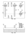
- FIG. 12A is a top-down view of the second exemplary structure after formation of gate structures according to the second embodiment of the present disclosure.
- FIG. 12B is a vertical cross-sectional view of the second exemplary structure along the vertical plane B-B′ of FIG. 12A .
- FIG. 13A is a top-down view of the second exemplary structure after formation of raised active regions and raised inactive regions according to the second embodiment of the present disclosure.
- FIG. 13B is a vertical cross-sectional view of the second exemplary structure along the vertical plane B-B′ of FIG. 13A .
- FIG. 14A is a top-down view of the second exemplary structure after formation of cavities through the handle substrate, the insulator layer, and a metal interconnect structure according to the second embodiment of the present disclosure.
- FIG. 14B is a vertical cross-sectional view of the second exemplary structure along the vertical plane B-B′ of FIG. 14A .
- FIG. 15A is a top-down view of the second exemplary structure after application of a gel, a nanoscale string, and external electrodes according to the second embodiment of the present disclosure.
- FIG. 15B is a vertical cross-sectional view of the second exemplary structure along the vertical plane B-B′ of FIG. 8A .
- FIG. 16A is a top-down view of a first variation of the second exemplary structure after according to the second embodiment of the present disclosure.
- FIG. 16B is a vertical cross-sectional view of the first variation of the second exemplary structure along the vertical plane B-B′ of FIG. 16A .
- FIG. 17A is a top-down view of a second variation of the second exemplary structure according to the second embodiment of the present disclosure.
- FIG. 17B is a vertical cross-sectional view of the second variation of the second exemplary structure along the vertical plane B-B′ of FIG. 17A .
- FIG. 18A is a top-down view of a third exemplary structure after formation of gate structures and dummy gate structures according to a third embodiment of the present disclosure.
- FIG. 18B is a vertical cross-sectional view of the third exemplary structure along the vertical plane B-B′ of FIG. 18A .
- FIG. 19A is a top-down view of the third exemplary structure after formation of raised active regions according to the third embodiment of the present disclosure.
- FIG. 19B is a vertical cross-sectional view of the third exemplary structure along the vertical plane B-B′ of FIG. 19A .
- FIG. 20A is a top-down view of the third exemplary structure after formation of cavities through the handle substrate, the insulator layer, and a metal interconnect structure according to the third embodiment of the present disclosure.
- FIG. 20B is a vertical cross-sectional view of the third exemplary structure along the vertical plane B-B′ of FIG. 20A .
- FIG. 21A is a top-down view of the third exemplary structure after application of a gel, a nanoscale string, and external electrodes according to the third embodiment of the present disclosure.
- FIG. 21B is a vertical cross-sectional view of the third exemplary structure along the vertical plane B-B′ of FIG. 21A .
- FIG. 22A is a top-down view of a first variation of the third exemplary structure after according to the third embodiment of the present disclosure.
- FIG. 22B is a vertical cross-sectional view of the first variation of the third exemplary structure along the vertical plane B-B′ of FIG. 22A .
- FIG. 23A is a top-down view of a second variation of the third exemplary structure according to the third embodiment of the present disclosure.
- FIG. 23B is a vertical cross-sectional view of the second variation of the third exemplary structure along the vertical plane B-B′ of FIG. 23A .
- the present disclosure relates to electrode devices including a pair of electrodes laterally separated by a nanochannel, and a method of manufacturing the same.
- a structural element is referred to as being “on” another structural element when the structural element is located directly on the other structural element or when a set of at least one intervening element making direct physical contact with the structural element and the other structural element is present.
- a structural element is referred to as being “directly on” another structural element when there is no intervening structural element and a physical contact is formed between the structural element and the other structural element.
- an element is referred to as being “connected” or “coupled” to another element when the element is directly connected or coupled to the other element or when a set of at least one intervening element provides connection or coupling with the element and the other element.
- An element is referred to as being “directly connected” or “directly coupled” to another element when there is no intervening element and the connection or coupling is provided between the element and the other element.
- An element “abuts” another element when a physical interface area providing a direct contact is present between the element and the other element.
- a first exemplary structure according to a first embodiment of the present disclosure includes semiconductor fins ( 30 A, 30 B, 30 C) formed on an insulator layer 20 .
- the semiconductor fins ( 30 A, 30 B, 30 C) can be formed by providing a semiconductor-on-insulator (SOI) substrate including a handle substrate 10 , an insulator layer 20 (which is commonly referred to as a buried insulator layer), and a top semiconductor layer including a semiconductor material, and by patterning the top semiconductor layer into the semiconductor fins ( 30 A, 30 B, 30 C) employing methods known in the art.
- SOI semiconductor-on-insulator
- the semiconductor material of the semiconductor fins ( 30 A, 30 B, 30 C) is herein referred to as a first semiconductor material.
- the first semiconductor material can be an elemental semiconductor material or an alloy thereof, a compound semiconductor material, or an organic semiconductor material.
- the first semiconductor material can be a single crystalline semiconductor material.
- the first semiconductor material can be single crystalline silicon, a single crystalline silicon-germanium alloy, a single crystalline silicon-carbon alloy, or a single crystalline silicon-germanium-carbon alloy.
- Various portions of the semiconductor fins ( 30 A, 30 B, 30 C) may be doped with different dopant types and/or at different dopant concentrations as needed.
- Each semiconductor fin ( 30 A, 30 B, or 30 C) can have a parallel pair of lengthwise sidewalls and a parallel pair of end walls.
- the parallel pair of lengthwise sidewalls is parallel to the lengthwise direction of the semiconductor fin ( 30 A, 30 B, or 30 C).
- the lengthwise direction is the horizontal direction which passes through the center of mass of an element and around which the moment of inertia of the elements is at the minimum.
- the parallel pair of end walls can be perpendicular to the lengthwise direction for each semiconductor fin ( 30 A, 30 B, 30 C).
- each semiconductor fin ( 30 A, 30 B, or 30 C), as measured along the horizontal direction perpendicular to the lengthwise direction of the semiconductor fin ( 30 A, 30 B, or 30 C), can be in a range from 5 nm to 80 nm, although lesser and greater widths can also be employed.
- the height of each semiconductor fin ( 30 A, 30 B, or 30 C) can be in a range from 5 nm to 200 nm, although lesser and greater heights can also be employed.
- the semiconductor fins ( 30 A, 30 B, 30 C) can include a parallel pair of semiconductor fins ( 30 A, 30 B) that are subsequently employed as portions of a parallel pair of electrodes, and can include device semiconductor fins 30 C, which can be employed to form conventional semiconductor devices as known in the art (such as fin field effect transistors).
- a device semiconductor fin refers to a semiconductor fin to form fin-based semiconductor devices as known in the art.
- gate structures ( 40 , 42 , 48 , 56 ) are formed across one or more of the semiconductor fins ( 30 A, 30 B, 30 C).
- Each gate structure ( 40 , 42 , 48 , 56 ) can include a gate dielectric 40 and a gate electrode 42 , and can optionally include a gate dielectric cap 48 and/or a gate spacer 56 including a dielectric material.
- a gate structure ( 40 , 42 , 48 , 56 ) can be formed across at least one of the semiconductor fins ( 30 A, 30 B) among the parallel pair of semiconductor fins ( 30 A, 30 B).
- a gate structure ( 40 , 42 , 48 , 56 ) can be formed across each of the semiconductor fins ( 30 A, 30 B) among the parallel pair of semiconductor fins ( 30 A, 30 B). In one embodiment, the gate structures ( 40 , 42 , 48 , 56 ) may not be formed across the parallel pair of semiconductor fins ( 30 A, 30 B).
- the gate electrodes 42 may employ a non-conductive material. Further, the gate dielectrics 40 are formed as temporary structures, the gate dielectrics 40 may be replaced with a different disposable structure that can be removed selective to the semiconductor material of the semiconductor fins ( 30 A, 30 B, 30 C).
- a selective deposition process can be optionally performed to form various raised semiconductor regions, which can be subsequently doped or in-situ doped during the selective deposition process to form various raised active regions ( 32 A, 32 B, 34 , 36 ).
- an “active region” refers to a doped semiconductor material portion.
- a “raised active region” refers to a doped semiconductor material portion that is formed on a surface of a semiconductor fin.
- the selective deposition process deposits a semiconductor material, which is herein referred to as a second semiconductor material, on semiconductor surfaces while preventing deposition of the second semiconductor material on dielectric surfaces.
- a reactant gas that deposits the second semiconductor material and an etchant gas that etches the second semiconductor material are flowed simultaneously or alternately so that the net deposition rate of the second semiconductor material on crystalline surfaces is positive, while the net deposition rate of the second semiconductor material on amorphous surfaces is zero.
- the selective deposition process utilizes the growth rate differential of the second semiconductor material on crystalline surfaces and amorphous surfaces. It is well known that the growth rate of semiconductor materials is less on amorphous surfaces during a nucleation phase because nucleation of a semiconductor material on an amorphous surface proceeds at a much lower rate than deposition of the same semiconductor material on crystallographic surfaces due to kinematics of the growth process.
- the flow rate of the etchant gas is selected such that the etch rate of the second semiconductor material is less than the deposition rate of the second semiconductor material on crystalline surfaces and is greater than the nucleation rate of the second semiconductor material on dielectric surfaces.
- the selective deposition process can be a selective epitaxy process that deposits the second semiconductor material.
- the second semiconductor material can be any semiconductor material that can be deposited as a single crystalline material or a polycrystalline material.
- the second semiconductor material may be the same as, or may be different from, the first semiconductor material.
- the second semiconductor material can be single crystalline, in which can the second semiconductor material in the various raised active regions ( 32 A, 32 B, 34 , 36 ) can be epitaxially aligned to the semiconductor fins ( 30 A, 30 B, 30 C).
- Various portions of the semiconductor fins ( 30 A, 30 B, 30 C) may be doped suitably prior to, or after, the selective deposition process.
- the selective deposition process may deposit the second semiconductor material as an intrinsic semiconductor material, or as a doped semiconductor material.
- the second semiconductor material can be subsequently doped by introduction of p-type dopants and/or n-type dopants, for example, by ion implantation.
- portions of semiconductor fins ( 30 A, 30 B, 30 C) that underlie gate structures ( 40 , 42 , 48 , 56 ) can constitute body regions of field effect transistors.
- the raised active regions ( 32 A, 32 B, 34 , 36 ) include a first raised active region 32 A formed on at least a portion of the first semiconductor fin 30 A, and a second raised active region 32 B formed on at least a portion of the second semiconductor fin 30 B. At least one additional raised active region 34 can be formed on the first and/or second semiconductor fins ( 30 A, 30 B) if at least one gate structure ( 40 , 42 , 48 , 56 ) is present on the first and/or second semiconductor fins ( 30 A, 30 B).
- Device raised active regions 36 i.e., raised active regions that are employed as an element of a semiconductor device as known in the art, can be formed on device semiconductor fins 30 C.
- the first raised active region 32 A can contact the entirety of sidewall surfaces and the top surface of the first semiconductor fin 30 A, and the second raised active region 32 B can contact the entirety of sidewall surfaces and the top surface of the second semiconductor fin 30 B.
- the first semiconductor fin 30 A and elements contacting the first semiconductor fin 30 A and located over the insulator layer 20 can collectively constitute a first electrode ( 30 A, 32 A, 34 , 40 , 42 , 48 , 56 ).
- the second semiconductor fin 30 B and elements contacting the second semiconductor fin 30 B and located over the insulator layer 20 collectively constitute a second electrode ( 30 B, 32 B, 34 , 40 , 42 , 48 , 56 ).
- a gate stack ( 40 , 42 , 48 , 56 ) and an additional raised active region 34 may, or may not, be present.
- the semiconductor fins ( 30 A, 30 B, 30 C) can be single crystalline, and the various raised active regions ( 32 A, 32 B, 34 , 36 ) can be formed as single crystalline doped semiconductor material portions in epitaxial alignment with the single crystalline structure of underlying semiconductor fins ( 30 A, 30 B, 30 C).
- the various raised active regions ( 32 A, 32 B, 34 , 36 ) can be formed with crystallographic facets.
- the crystallographic orientations of the first and second semiconductor fins ( 30 A, 30 B) can be selected such that ridges at which two adjoining crystallographic facets are adjoined to one another runs parallel to each other between the first and second semiconductor fins ( 30 A, 30 B).
- a ridge of the first raised active region 32 A and a ridge of the second raised active region 32 B can be parallel to each other, and can be laterally spaced from each other by a spacing that is invariant under lateral translation along the lengthwise direction of the first and second semiconductor fins ( 30 A, 30 B).
- the invariant spacing is herein referred to as a width w of a nanochannel.
- the width w can be in a range from 0.5 nm to 100 nm.
- a nanochannel refers to a gap having a uniform width that is invariant under lateral translation and has a dimension less than 100 nm.
- a pair of parallel electrodes is formed on a substrate ( 10 , 20 ).
- Each of the pair of parallel electrodes includes at least a semiconductor fin ( 30 A or 30 B), and a nanochannel is formed between the pair of parallel electrodes.
- the pair of parallel electrodes can include a first electrode ( 30 A, 32 A, 34 , 40 , 42 , 48 , 56 ) and a second electrode ( 30 B, 32 B, 34 , 40 , 42 , 48 , 56 ).
- a planarization dielectric layer 60 can be formed over the gate structures ( 40 , 42 , 48 , 56 ) and planarized, for example, by chemical mechanical planarization.
- each stack of a dielectric gate cap 48 , a gate electrode 42 , and a gate dielectric 40 can be replaced with a permanent gate structure ( 50 , 52 ) that includes a replacement gate dielectric 50 and a replacement gate electrode 52 .
- At least one metal interconnect structure-containing layer ( 70 , 72 , 74 A, 74 B, 76 ) can be formed over the planarization dielectric layer 60 .
- the at least one metal interconnect structure-containing layer 70 includes conductive structures ( 72 , 74 A, 74 B, 76 ) embedded in at least one dielectric material layer 70 .
- the conductive structures ( 72 , 74 A, 74 B, 76 ) can include a first conductive structure 74 A that is electrically shorted to the first electrode ( 30 A, 32 A, 34 , 40 , 42 , 48 , 56 ), e.g., by physically contacting the additional raised active region 34 (See FIG.
- each of the first and second conductive structures ( 74 A, 74 B) is electrically shorted to one of the pair of parallel electrodes ( 30 A, 32 A, 30 B, 32 B, 34 , 40 , 42 , 48 , 56 ).
- the conductive structures ( 72 , 74 A, 74 B, 76 ) can further include gate contact conductive structures 72 that contact the gate electrodes 52 straddling the first or second semiconductor fins ( 30 A, 30 B). Further, the conductive structures ( 72 , 74 A, 74 B, 76 ) can include device contact conductive structures 76 , which provide electrical contact to various components of semiconductor devices formed employing the device semiconductor fins 30 C. For example, the device contact conductive structures 76 can be electrically shorted to a source region, a drain region, or a gate of a fin field effect transistor.
- the conductive structures ( 72 , 74 A, 74 B, 76 ) can include metal lines and/or metal vias as known in the art.
- the conductive structures ( 72 , 74 A, 74 B, 76 ) can be placed such that a region overlying the first and second raised active regions ( 32 A, 32 B) do not include any conductive structure ( 72 , 74 A, 74 B, 76 ).
- the handle substrate 10 can be thinned to a thickness in the range from 30 ⁇ m to 100 ⁇ m, for example, by grinding, polishing, or other mechanical and/or chemical means for thinning a substrate. Subsequently, the first exemplary structure can be flipped upside down so that the physically exposed horizontal surface of the handle substrate 10 is positioned at the top.
- a photoresist layer (not shown) can be applied over the physically exposed surface of the handle substrate 10 , and can be lithographically patterned to form an opening in a region overlying the gap between the first semiconductor fin 30 A and the second semiconductor gap 30 B.
- the pattern in the photoresist layer can be transferred through the handle substrate 10 by an etch, which can be an isotropic etch or an anisotropic etch. In one embodiment, the etch can be selective to the dielectric material of the insulator layer 20 .
- a cavity that replicates the shape of the photoresist layer can be formed within the handle substrate 10 , which is herein referred to as a handle substrate cavity 11 .
- a cavity is formed through the insulator layer 20 , which is herein referred to as an insulator cavity 21 .
- the insulator cavity 21 and the handle substrate cavity 11 collectively constitute a contiguous cavity in the substrate ( 10 , 20 ).
- the photoresist layer employed to pattern the handle substrate cavity 11 can be removed, and a new photoresist layer may be applied and patterned to serve as the template for a pattern transfer into the insulator layer, for example, by an isotropic etch or an anisotropic etch.
- the new photoresist layer can be subsequently removed, for example, by ashing.
- the photoresist layer may be removed, and a permanent spacer or a disposable spacer can be formed on the sidewalls of the handle substrate 10 around the handle substrate cavity 11 , and can be employed as the template for a pattern transfer into the insulator layer, for example, by an isotropic etch or an anisotropic etch.
- the photoresist layer and/or the handle substrate 10 can be employed as a template for a pattern transfer into the insulator layer, for example, by an isotropic etch or an anisotropic etch.
- the handle substrate cavity 11 and the insulator cavity 21 can have vertically coincident sidewalls.
- two surfaces are “vertically coincident” if there exists a vertical plane that includes the two surfaces.
- Other methods of forming a cavity in a substrate can also be employed to form a contiguous cavity ( 11 , 21 ) that includes the handle substrate cavity 11 and the insulator cavity 21 .
- the locations of the sidewalls of the insulator cavity 21 are selected such the cavity through the insulator layer 20 does not extend outside of the region defined by a pair of distal lengthwise sidewalls (DSL 1 , DSL 2 ) of the first and second semiconductor fins ( 30 A, 30 B).
- the locations of the sidewalls of the insulator cavity 21 are selected such that a first sidewall of the insulator cavity is positioned within an area defined by a first distal lengthwise sidewall of the first semiconductor fin 30 A and the ridge of the first raised active region 32 A that defines the width w, while a second sidewall SW 2 of the insulator cavity 21 is positioned within an area defined by a second distal lengthwise sidewall DLS 2 of the second semiconductor fin 30 B and the ridge of the second raised active region 32 B that defines the width w.
- a cavity which is herein referred to as a dielectric layer cavity 61 , is formed though the at least one dielectric material layer 70 and the planarization dielectric layer 60 .
- the dielectric layer cavity 61 can be formed so that the area of the dielectric layer cavity 61 overlap with the area of the insulator cavity 20 within an area defined by a portion of the nanochannel having the width w and laterally bounded by the first raised active region 32 A and the second raised active region 32 B.
- the dielectric layer cavity 61 can be formed by etching a region of the at least one dielectric material layer 70 over the pair of parallel electrodes ( 30 A, 30 B, 32 A, 32 B, 50 , 52 , 56 , 34 ) such that sidewalls of the dielectric layer cavity 61 vertically extend from a topmost surface of the contiguous cavity ( 11 , 21 , 61 ) to a horizontal surface of the substrate ( 10 , 20 ) and surfaces of the pair of parallel electrodes ( 30 A, 30 B, 32 A, 32 B, 50 , 52 , 56 , 34 ), and specifically, surfaces of the first and second raised active regions ( 30 A, 30 B).
- the etching can be performed, for example, by an anisotropic etch employing a temporary etch mask such as a patterned photoresist layer.
- the sidewalls of the dielectric layer cavity 61 may, or may not, be vertical.
- the overlap between the nanochannel bounded by the first raised active region 32 A and the second raised active region 32 B and the area of the dielectric layer cavity 61 defines a nanochannel NC.
- the nanochannel NC is defined by a parallel pair of proximal ridges of the first raised active region 30 A and the second raised active region 30 B that are separated by the width w and a pair of vertical sidewalls of the dielectric layer cavity 61 that are spaced from each other by a length L.
- the nanochannel NC can have a rectangular cross-sectional shape in which a pair of sides has the dimension of the width w and another pair of sides has the dimension of the length L.
- the width w can be in a range from 0.5 nm to 100 nm
- the length L can be in a range from 2 nm to 10,000 nm.
- the set of the handle substrate cavity 11 , the insulator cavity 21 , and the dielectric layer cavity 61 collectively constitute a contiguous cavity ( 11 , 21 , 61 ).
- the least cross-sectional area along contiguous paths from the top of the contiguous cavity ( 11 , 21 , 61 ) and the bottom of the contiguous cavity ( 11 , 21 , 61 ) occurs at the nanochannel having the width w and the length L.
- the contiguous cavity ( 11 , 21 , 61 ) passes through the substrate ( 10 , 20 ) and the metal interconnect structure-containing layer ( 70 , 72 , 74 A, 74 B, 76 ) and includes the nanochannel NC.
- the nanochannel NC can have a rectangular periphery having the width w in a range from 0.5 nm to 100 nm, and the length L that is greater than the width.
- the width w can be perpendicular to the lengthwise direction of the semiconductor fins ( 30 A, 30 B) and the length can be parallel to the lengthwise direction of the semiconductor fins ( 30 A, 30 B).
- Each of the pair of parallel electrodes ( 30 A, 30 B, 32 A, 32 B, 50 , 52 , 56 , 34 ) can include a raised active region ( 32 A or 32 B) including a doped semiconductor material.
- the nanochannel NC can have a periphery including edges of the raised active regions ( 32 A, 32 B).
- the periphery of the nanochannel NC can further include two portions of sidewalls of the at least one dielectric material layer located within the metal interconnect structure-containing layer ( 70 , 72 , 74 A, 74 B, 76 ).
- the sidewalls can be surfaces defining a lateral extent of the contiguous cavity ( 11 , 21 , 61 ), and specifically, defining the length L of the dielectric layer cavity 61 portion of the contiguous cavity ( 11 , 21 , 61 ).
- a medium 90 can be applied in the contiguous cavity ( 11 , 21 , 61 ).
- a “medium” or a “material transport medium” refers to a material through which transport of an embedded material is possible.
- the medium 90 can be an electrophoresis gel as known in the art.
- the medium 90 can be a solution in which molecules or other materials can be transported. In this case, the solution can be an aqueous solution.
- the medium 90 can include at least one nanoscale string 91 .
- the medium 90 can be disposed within the contiguous cavity ( 11 , 21 , 61 ) and optionally above or below the first exemplary structure.
- nanoscale string refers to an elongated structure extending predominantly along one direction and having dimensions that are less than 100 nm along directions perpendicular to the local lengthwise direction of the elongated structure.
- the local lengthwise direction of a nanoscale string can gradually change so that twists and turns in the global structure of the nanoscale string are possible.
- Typical examples of a nanoscale string include DNA strands and carbon nanotubes.
- External electrodes ( 92 , 12 ) can be disposed across the nanochannel NC.
- a first external electrode 92 can be disposed above the top surface of the substrate ( 10 , 20 ) and on the medium 90
- the second external electrode 12 can be disposed below the top surface of the substrate ( 10 , 20 ) and on the medium 90 .
- a first external electrode 92 can be disposed over the nanochannel NC and within the portion of the medium 90 overlying the nanochannel NC
- a second external electrode 12 can be disposed under the nanochannel NC and within the portion of the medium 90 underlying the nanochannel NC.
- the first exemplary structure may be oriented in any convenient orientation to facilitate positioning of the first and second external electrodes ( 92 , 12 ).
- first external electrode 92 and the second external electrode 12 can be electrically biased with respect to each other to induce flow of electrically charged material in the medium 90 and through the nanochannel NC.
- a leakage current measurement circuitry can be connected to the first conductive structure 74 A and the second conductive structure 74 B to enable measurement of the change in the leakage current through the nanochannel NC as a nanoscale string passes through the nanochannel NC.
- the leakage current measurement circuitry can be configured to measure the leakage current through the pair of parallel electrodes ( 30 A, 30 B, 32 A, 32 B, 50 , 52 , 34 ) and a portion of the electrically charged material within the nanochannel NC, which can be a nanoscale string passing through the nanochannel NC due to the electrical bias voltage applied across the first external electrode 92 and the second external electrode 12 .
- a pair of parallel electrodes ( 30 A, 30 B, 32 A, 32 B, 50 , 52 , 34 ) is located on a substrate ( 10 , 20 ).
- Each of the pair of parallel electrodes ( 30 A, 30 B, 32 A, 32 B, 50 , 52 , 34 ) includes at least a semiconductor fin ( 30 A or 30 B), and a nanochannel NC is present between the pair of parallel electrodes ( 30 A, 30 B, 32 A, 32 B, 50 , 52 , 34 ).
- a metal interconnect structure-containing layer ( 70 , 72 , 74 A, 74 B, 76 ) is present over the substrate ( 10 , 20 ).
- Conductive structures ( 72 , 74 A, 74 B, 76 ) are embedded in at least one dielectric material layer 70 .
- the conductive structures ( 72 , 74 A, 74 B, 76 ) includes a first conductive structure 74 A that is electrically shorted to the first electrode ( 30 A, 32 A, 50 , 52 , 34 ) among the pair of parallel electrodes, and further includes a second conductive structure 74 B that is electrically shorted to the second electrode ( 30 B, 32 B, 50 , 52 , 34 ) among the pair of parallel electrodes.
- the first exemplary structure is an electrophoresis system that enables leakage current measurement as the nanoscale string 91 passes through the nanochannel NC.
- a first variation of the first exemplary structure can be derived from the first exemplary structure by omitting formation of the various raised active regions ( 32 A, 332 B, 34 , 36 ) at the processing steps of FIGS. 3A and 3B , i.e., by skipping the selective deposition process that forms the various raised active regions ( 32 A, 332 B, 34 , 36 ) of the first exemplary structure.
- the width of the nanochannel can be the same as the lateral distance between a proximal pair of lengthwise sidewalls of the first and second semiconductor fins ( 30 A, 30 B), i.e., the lateral distance between the lengthwise sidewall of the first semiconductor fin 30 A that is proximal to the second semiconductor fin 30 B and the lengthwise sidewall of the second semiconductor fin 30 B that is proximal to the first semiconductor fin 30 A.
- a second variation of the first exemplary structure can be derived from the first exemplary structure or the first variation of the first exemplary structure by employing a bulk semiconductor substrate in lieu of an SOI substrate.
- semiconductor fins 30 A, 30 B, 30 C
- a shallow trench isolation layer 120 can be deposited over the top surface of the semiconductor substrate 110 such that the shallow trench isolation layer 120 laterally surrounds lower portions of each semiconductor fin ( 30 A, 30 B, 30 C).
- FIGS. 2A , 2 B, 3 A, 3 B, 4 A, 4 B, 5 A, and 5 B can be subsequently performed.
- the processing steps of FIGS. 3A and 3B can be omitted.
- the semiconductor substrate 110 can be thinned, and a cavity can be formed through the semiconductor substrate 110 .
- an overetch into the shallow trench isolation layer 120 may cause sidewalls within the semiconductor substrate 110 to be vertically coincident with sidewalls within the shallow trench isolation layer 120 .
- High selectivity of the etch process to the material of the shallow trench isolation layer during formation of the cavity in the semiconductor substrate 110 can reduce or remove the etching into the shallow trench isolation layer.
- Another cavity which is herein referred to as an insulator cavity, is formed through the shallow trench isolation layer 120 .
- the locations of the sidewalls of the insulator cavity are selected such the insulator cavity through the shallow trench isolation layer 120 does not extend outside of the region defined by a pair of distal lengthwise sidewalls (DLS 1 , DLS 2 ) of the first and second semiconductor fins ( 30 A, 30 B).
- the processing steps of FIGS. 7A , 7 B, 8 A, and 8 B can be performed to provide the second variation of the first exemplary structure.
- a second exemplary structure according to a second embodiment of the present disclosure is formed by modifying the layout of the semiconductor fins ( 30 A, 30 B, 30 C, 30 D) from the layout illustrated in FIG. 1A .
- at least one additional semiconductor fin 30 D is formed between the first semiconductor fin 30 A and the second semiconductor fin 30 B.
- at least one pair of additional semiconductor fins 30 D can be formed between the first semiconductor fin 30 A and the second semiconductor fin 30 B such that there exist a sufficient gap between the first and second semiconductor fins ( 30 A, 30 B) that is not filled with selectively deposited semiconductor material in a subsequent selective deposition of a second semiconductor material.
- gate structures ( 40 , 42 , 48 , 56 ) can be formed employing the same methods as in the first embodiment.
- the gate structures ( 40 , 42 , 48 , 56 ) may, or may not, be formed on the first and/or second semiconductor fins ( 30 A, 30 B), and may, or may not, be formed on the additional semiconductor fins 30 D.
- the entirety of each of the first and second semiconductor fins ( 30 A, 30 B) can be doped with dopants of the same conductivity type, which can be p-type or n-type, so that the entirety of each semiconductor fin ( 30 A, 30 B) is a conductive structure.
- a selective deposition process can be optionally performed to form various raised semiconductor regions.
- a subset of the various semiconductor regions can be subsequently doped to form various raised active regions ( 32 A, 32 B, 34 , 36 ).
- Another subset of the various semiconductor regions can remain undoped, and constitute raised inactive regions 34 , which are semiconductor regions that are not doped.
- an “inactive region” refers to an undoped semiconductor material portion, which can be substantially intrinsic and have high enough resistivity (>1.0 ⁇ 10 3 Ohm-cm) to be treated as an insulator.
- a “raised inactive region” refers to an undoped semiconductor material portion that is formed on a surface of a semiconductor fin.
- the selective deposition process deposits a semiconductor material, which is herein referred to as a second semiconductor material, on semiconductor surfaces while preventing deposition of the second semiconductor material on dielectric surfaces.
- the selective deposition process can be the same as in the first embodiment provided that in-situ doping is not employed in the second embodiment.
- the selective deposition process can be a selective epitaxy process that deposits the second semiconductor material.
- the second semiconductor material can be any semiconductor material that can be deposited as a single crystalline material or a polycrystalline material.
- the second semiconductor material may be the same as, or may be different from, the first semiconductor material.
- the second semiconductor material can be single crystalline, in which can the second semiconductor material in the various raised active regions ( 32 A, 32 B, 34 , 36 ) can be epitaxially aligned to the semiconductor fins ( 30 A, 30 B, 30 C).
- Various portions of the semiconductor fins ( 30 A, 30 B, 30 C) may be doped suitably prior to, or after, the selective deposition process.
- fin source regions (not shown) and fin drain regions (not shown) can be formed in various portions of the semiconductor fins ( 30 A, 30 B, 30 C) by ion implantation and/or diffusion from the raised active regions ( 32 A, 32 B, 34 , 36 ) and/or by other methods known in the art.
- the selective deposition process may deposit the second semiconductor material as an intrinsic semiconductor material.
- portions of semiconductor fins ( 30 A, 30 B, 30 C) that underlie gate structures ( 40 , 42 , 48 , 56 ) can constitute body regions of field effect transistors.
- the raised active regions ( 32 A, 32 B, 34 , 36 ) include a first raised active region 32 A formed on at least a portion of the first semiconductor fin 30 A, and a second raised active region 32 B formed on at least a portion of the second semiconductor fin 30 B. At least one additional raised active region 34 can be formed on the first and/or second semiconductor fins ( 30 A, 30 B) if at least one gate structure ( 40 , 42 , 48 , 56 ) is present on the first and/or second semiconductor fins ( 30 A, 30 B).
- Device raised active regions 36 i.e., raised active regions that are employed as an element of a semiconductor device as known in the art, can be formed on device semiconductor fins 30 C.
- the first raised active region 32 A can contact the entirety of sidewall surfaces and the top surface of the first semiconductor fin 30 A, and the second raised active region 32 B can contact the entirety of sidewall surfaces and the top surface of the second semiconductor fin 30 B.
- the first semiconductor fin 30 A and elements contacting the first semiconductor fin 30 A and located over the insulator layer 20 can collectively constitute a first electrode ( 30 A, 32 A, 34 , 40 , 42 , 48 , 56 )
- the second semiconductor fin 30 B and elements contacting the second semiconductor fin 30 B and located over the insulator layer 20 collectively constitute a second electrode ( 30 B, 32 B, 34 , 40 , 42 , 48 , 56 ).
- a gate stack ( 40 , 42 , 48 , 56 ) and an additional raised active region 34 may, or may not, be present.
- the semiconductor fins ( 30 A, 30 B, 30 C) can be single crystalline, and the various raised active regions ( 32 A, 32 B, 34 , 36 ) can be formed as single crystalline doped semiconductor material portions in epitaxial alignment with the single crystalline structure of underlying semiconductor fins ( 30 A, 30 B, 30 C).
- the various raised active regions ( 32 A, 32 B, 34 , 36 ) can be formed with crystallographic facets.
- the crystallographic orientations of the first and second semiconductor fins ( 30 A, 30 B) can be selected such that ridges at which two adjoining crystallographic facets are adjoined to one another runs parallel to each other between the first and second semiconductor fins ( 30 A, 30 B).
- a ridge of the first raised active region 32 A and a ridge of the second raised active region 32 B can be parallel to each other, and can be laterally spaced from each other by a spacing that is invariant under lateral translation along the lengthwise direction of the first and second semiconductor fins ( 30 A, 30 B).
- the invariant spacing is herein referred to as a width w of a nanochannel.
- the width w can be in a range from 10 nm to 1,000 nm.
- a nanochannel refers to a gap having a uniform width that is invariant under lateral translation and has a dimension less than 100 nm.
- a pair of parallel electrodes is formed on a substrate ( 10 , 20 ).
- Each of the pair of parallel electrodes includes at least a semiconductor fin ( 30 A or 30 B), and a nanochannel is formed between the pair of parallel electrodes.
- the pair of parallel electrodes can include a first electrode ( 30 A, 32 A, 34 , 40 , 42 , 48 , 56 ) and a second electrode ( 30 B, 32 B, 34 , 40 , 42 , 48 , 56 ).
- Raised inactive regions 33 can be formed on the additional semiconductor fins 30 D.
- the raised inactive regions 33 include undoped semiconductor material.
- the raised inactive regions 33 can be formed by performing the selective deposition process and preventing implantation of electrical dopants into the semiconductor material portions deposited directly on the additional semiconductor fins 30 D, while implanting p-type dopants and/or n-type dopants to form the various raised active regions ( 32 A, 32 B, 34 , 36 ).
- the lateral distances between neighboring semiconductor fins ( 30 A, 30 B, 30 C, 30 D) are selected such that the raised inactive regions 33 adjoin the first raised active region 32 A and the second raised active regions 32 B.
- a rectangular opening defined by inner peripheries of the first and second raised active regions ( 32 A, 32 B) and the raised inactive regions 33 can be formed over the substrate ( 10 , 20 ).
- the opening can have a width w that is invariant along the lengthwise direction of the first and second semiconductor fins ( 30 A, 30 B) and a length L that is invariant along the horizontal direction that is perpendicular to the lengthwise direction of the first and second semiconductor fins ( 30 A, 30 B).
- a contiguous cavity ( 11 , 21 , 61 ) can be formed in the same manner as in the first embodiment.
- the nanochannel NC can be defined by a rectangular periphery having a width w in a range from 30 nm to 100 nm, and a length L that is greater than the width w. In one embodiment, the length L can be in a range from 100 nm to 10,000 nm.
- the locations of the sidewalls of the insulator cavity 21 can be selected such the cavity through the insulator layer 20 does not extend outside of the region defined by a pair of distal lengthwise sidewalls (DSL 1 , DSL 2 ) of the first and second semiconductor fins ( 30 A, 30 B).
- the processing steps of FIGS. 8A and 8B can be performed.
- the second exemplary structure of FIGS. 15A and 15B can be an electrophoresis system or a solution-based material transport system, and may be operated in the same manner as in the first embodiment illustrated in FIGS. 8A , 8 B, 9 A, 9 B, 10 A, and 10 B.
- a first variation of the second exemplary structure can be derived from the second exemplary structure by omitting the selective deposition process illustrated in FIGS. 13A and 13B .
- the length L of the nanochannel NC can be defined by the dimensions of the cavity through the at least one dielectric material layer 70 along the lengthwise direction of the first and second semiconductor fins ( 30 A, 30 B) that are parallel to each other.
- the width w of the nanochannel NC can be defined by the distance between a pair of proximal lengthwise sidewalls of the first semiconductor fins 30 A and the second semiconductor fin 30 B.
- a second variation of the second exemplary structure can be derived from the second exemplary structure or the first variation of the second exemplary structure by employing a bulk semiconductor substrate and employing a shallow trench isolation layer 120 in lieu of an insulator layer 20 .
- a third exemplary structure according to a third embodiment of the present disclosure can be derived from the first exemplary structure of FIGS. 1A and 1B by performing the processing steps of FIGS. 2A and 2B and concurrently forming at least one dummy gate structure ( 140 , 142 , 148 , 156 ) across the first semiconductor fin 30 A and the second semiconductor fin 30 B.
- the at least one dummy gate structure ( 140 , 142 , 148 , 156 ) can have the same stack of material layers as the gate structures ( 40 , 42 , 48 , 56 ), and can be formed as additional patterned structures that are patterned simultaneously with formation of the gate structures ( 40 , 42 , 48 , 56 ).
- the entirety of each of the first and second semiconductor fins ( 30 A, 30 B) can be doped with dopants of the same conductivity type, which can be p-type or n-type, so that the entirety of each semiconductor fin ( 30 A, 30 B) is a conductive structure.
- a pair of dummy gate structures ( 140 , 142 , 148 , 156 ) can be positioned such that a pair of proximal sidewalls of the dummy gate structures ( 140 , 142 , 148 , 156 ), e.g., a proximal pair of sidewalls of dummy gate spacers 156 , is separated from each other by a length L, which is the length of a nanochannel to be subsequently formed.
- the direction of separation of the pair of proximal sidewalls of the dummy gate structures ( 140 , 142 , 148 , 156 ) can be the lengthwise direction of the first and second semiconductor fins ( 30 A, 30 B).
- a dummy gate structure ( 140 , 142 , 148 , 156 ) does not function as a gate of a transistor, the portion of the first and/or second semiconductor fin ( 30 A, 30 B) that underlies such a dummy gate structure ( 140 , 142 , 148 , 156 ) can be doped with p-type dopants or n-type dopants to electrically short the two portions of the semiconductor fin ( 30 A, 30 B) laterally spaced by the width of the dummy gate structure ( 140 , 142 , 148 , 156 ).
- the processing steps of FIGS. 3A and 3B are performed to form various raised active regions ( 32 A, 32 B, 34 , 36 ).
- the first raised active region 32 A formed on the first semiconductor fin 30 A and the second raised active region 32 B formed on the second semiconductor fin 30 B can be laterally spaced from each other by a width w, which is the width of a nanochannel.
- a contiguous cavity ( 11 , 21 , 61 ) can be formed in the same manner as in the first embodiment.
- the nanochannel NC can be defined by a rectangular periphery having a width w in a range from 0.5 nm to 100 nm, and a length L that is greater than the width w. In one embodiment, the length L can be in a range from 100 nm to 10,000 nm.
- the locations of the sidewalls of the insulator cavity 21 can be selected such the cavity through the insulator layer 20 does not extend outside of the region defined by a pair of distal lengthwise sidewalls (DSL 1 , DSL 2 ) of the first and second semiconductor fins ( 30 A, 30 B).
- the length L of the nanochannel NC can be defined by the lateral spacing between the pair of proximal sidewalls of the two dummy gate structures ( 140 , 142 , 148 , 156 ).
- the length L of the nanochannel NC can be defined by the lateral spacing between the outer sidewall of the gate spacer 56 that is proximal to the dummy gate structure ( 140 , 142 , 148 . 156 ) and the outer sidewall of the dummy gate spacer 156 that is proximal to the gate structure ( 40 , 42 , 48 , 56 ).
- the length L can be defined by the spacing between a pair of dummy gate structures ( 140 , 142 , 148 , 156 ) straddling the first and second semiconductor fins ( 30 A, 30 B), or by a pair of a dummy gate structure ( 140 , 142 , 148 , 156 ) and a gate structure ( 40 , 42 , 48 , 56 ).
- FIGS. 21A and 21B the processing steps of FIGS. 8A and 8B can be performed.
- the third exemplary structure of FIGS. 21A and 21B can be an electrophoresis system or a solution-based material transport system, and may be operated in the same manner as in the first embodiment illustrated in FIGS. 8A , 8 B, 9 A, 9 B, 10 A, and 10 B.
- a first variation of the third exemplary structure can be derived from the third exemplary structure by omitting the selective deposition process illustrated in FIGS. 19A and 19B .
- the width w of the nanochannel NC can be defined by the distance between a pair of proximal lengthwise sidewalls of the first semiconductor fins 30 A and the second semiconductor fin 30 B.
- a second variation of the third exemplary structure can be derived from the third exemplary structure or the first variation of the third exemplary structure by employing a bulk semiconductor substrate and employing a shallow trench isolation layer 120 in lieu of an insulator layer 20 .
- the various structures of the present disclosure provide a nanochannel NC, which can have a width w that can be on the order of nanometers or tens of nanometers. Further, the length L of the nanochannel NC can be selected as any dimension limited only by lithographic limitations.
- the various structures of the present disclosure can be employed to form a custom-tailored opening size for characterization of nanoscale strings that passes through the nanochannel during gel electrophoresis, a solution-based material transport and characterization, or by any other methods that induces movement of the nanoscale string through the nanochannel.
- the various structures of the present disclosure can be employed to characterize a nanoscale string such as a DNA string.
Abstract
Description
Claims (10)
Priority Applications (2)
| Application Number | Priority Date | Filing Date | Title |
|---|---|---|---|
| US14/452,741 US9228994B1 (en) | 2014-08-06 | 2014-08-06 | Nanochannel electrode devices |
| US14/987,329 US9557290B2 (en) | 2014-08-06 | 2016-01-04 | Nanochannel electrode devices |
Applications Claiming Priority (1)
| Application Number | Priority Date | Filing Date | Title |
|---|---|---|---|
| US14/452,741 US9228994B1 (en) | 2014-08-06 | 2014-08-06 | Nanochannel electrode devices |
Related Child Applications (1)
| Application Number | Title | Priority Date | Filing Date |
|---|---|---|---|
| US14/987,329 Division US9557290B2 (en) | 2014-08-06 | 2016-01-04 | Nanochannel electrode devices |
Publications (1)
| Publication Number | Publication Date |
|---|---|
| US9228994B1 true US9228994B1 (en) | 2016-01-05 |
Family
ID=54939131
Family Applications (2)
| Application Number | Title | Priority Date | Filing Date |
|---|---|---|---|
| US14/452,741 Expired - Fee Related US9228994B1 (en) | 2014-08-06 | 2014-08-06 | Nanochannel electrode devices |
| US14/987,329 Expired - Fee Related US9557290B2 (en) | 2014-08-06 | 2016-01-04 | Nanochannel electrode devices |
Family Applications After (1)
| Application Number | Title | Priority Date | Filing Date |
|---|---|---|---|
| US14/987,329 Expired - Fee Related US9557290B2 (en) | 2014-08-06 | 2016-01-04 | Nanochannel electrode devices |
Country Status (1)
| Country | Link |
|---|---|
| US (2) | US9228994B1 (en) |
Cited By (2)
| Publication number | Priority date | Publication date | Assignee | Title |
|---|---|---|---|---|
| US10388519B2 (en) * | 2017-08-16 | 2019-08-20 | Tokyo Electron Limited | Method and device for incorporating single diffusion break into nanochannel structures of FET devices |
| LU101020B1 (en) * | 2018-11-28 | 2020-05-28 | Luxembourg Inst Science & Tech List | Ion-sensitive field effect transistor |
Families Citing this family (2)
| Publication number | Priority date | Publication date | Assignee | Title |
|---|---|---|---|---|
| CN111094976B (en) | 2018-02-16 | 2022-05-13 | 伊鲁米纳公司 | Apparatus for sequencing |
| EP4075131A1 (en) * | 2021-04-16 | 2022-10-19 | Imec VZW | Nanopore transistor for biosensing |
Citations (18)
| Publication number | Priority date | Publication date | Assignee | Title |
|---|---|---|---|---|
| US6515847B1 (en) | 1998-09-30 | 2003-02-04 | Nippon Chemi-Con Corporation | Solid electrolyte capacitor and its manufacturing method |
| US6627067B1 (en) | 1999-06-22 | 2003-09-30 | President And Fellows Of Harvard College | Molecular and atomic scale evaluation of biopolymers |
| US6638885B1 (en) | 1997-05-22 | 2003-10-28 | The Trustees Of Princeton University | Lyotropic liquid crystalline L3 phase silicated nanoporous monolithic composites and their production |
| US6960298B2 (en) | 2001-12-10 | 2005-11-01 | Nanogen, Inc. | Mesoporous permeation layers for use on active electronic matrix devices |
| US7045851B2 (en) | 2003-06-20 | 2006-05-16 | International Business Machines Corporation | Nonvolatile memory device using semiconductor nanocrystals and method of forming same |
| US7098393B2 (en) | 2001-05-18 | 2006-08-29 | California Institute Of Technology | Thermoelectric device with multiple, nanometer scale, elements |
| US7217562B2 (en) | 2002-04-16 | 2007-05-15 | Princeton University | Gradient structures interfacing microfluidics and nanofluidics, methods for fabrication and uses thereof |
| US7223894B2 (en) | 2003-01-31 | 2007-05-29 | Institut Francais Du Petrole | Process for total hydrogenation using a catalytic reactor with a hydrogen-selective membrane |
| US7248771B2 (en) | 2003-06-16 | 2007-07-24 | Brigham Young University | Integrated sensor with electrical and optical single molecule sensitivity |
| US7250544B2 (en) | 2003-01-31 | 2007-07-31 | Institut Francais Du Petrole | Process for selective hydrogenation using a catalytic reactor with a hydrogen-selective membrane |
| US7274078B2 (en) | 2001-07-25 | 2007-09-25 | Nantero, Inc. | Devices having vertically-disposed nanofabric articles and methods of making the same |
| US7444053B2 (en) | 2003-06-16 | 2008-10-28 | The Regents Of The University Of California | Integrated electrical and optical sensor for biomolecule analysis with single molecule sensitivity |
| US7582490B2 (en) | 1999-06-22 | 2009-09-01 | President And Fellows Of Harvard College | Controlled fabrication of gaps in electrically conducting structures |
| US7586618B2 (en) | 2005-02-28 | 2009-09-08 | The Board Of Trustees Of The University Of Illinois | Distinguishing non-resonant four-wave-mixing noise in coherent stokes and anti-stokes Raman scattering |
| US7610074B2 (en) | 2004-01-08 | 2009-10-27 | The Board Of Trustees Of The University Of Illinois | Multi-functional plasmon-resonant contrast agents for optical coherence tomography |
| US7623908B2 (en) | 2003-01-24 | 2009-11-24 | The Board Of Trustees Of The University Of Illinois | Nonlinear interferometric vibrational imaging |
| US7626246B2 (en) | 2005-07-26 | 2009-12-01 | Amberwave Systems Corporation | Solutions for integrated circuit integration of alternative active area materials |
| US8384195B2 (en) | 2010-05-04 | 2013-02-26 | Imec | Nanochannel device and method for manufacturing thereof |
-
2014
- 2014-08-06 US US14/452,741 patent/US9228994B1/en not_active Expired - Fee Related
-
2016
- 2016-01-04 US US14/987,329 patent/US9557290B2/en not_active Expired - Fee Related
Patent Citations (18)
| Publication number | Priority date | Publication date | Assignee | Title |
|---|---|---|---|---|
| US6638885B1 (en) | 1997-05-22 | 2003-10-28 | The Trustees Of Princeton University | Lyotropic liquid crystalline L3 phase silicated nanoporous monolithic composites and their production |
| US6515847B1 (en) | 1998-09-30 | 2003-02-04 | Nippon Chemi-Con Corporation | Solid electrolyte capacitor and its manufacturing method |
| US7582490B2 (en) | 1999-06-22 | 2009-09-01 | President And Fellows Of Harvard College | Controlled fabrication of gaps in electrically conducting structures |
| US6627067B1 (en) | 1999-06-22 | 2003-09-30 | President And Fellows Of Harvard College | Molecular and atomic scale evaluation of biopolymers |
| US7098393B2 (en) | 2001-05-18 | 2006-08-29 | California Institute Of Technology | Thermoelectric device with multiple, nanometer scale, elements |
| US7274078B2 (en) | 2001-07-25 | 2007-09-25 | Nantero, Inc. | Devices having vertically-disposed nanofabric articles and methods of making the same |
| US6960298B2 (en) | 2001-12-10 | 2005-11-01 | Nanogen, Inc. | Mesoporous permeation layers for use on active electronic matrix devices |
| US7217562B2 (en) | 2002-04-16 | 2007-05-15 | Princeton University | Gradient structures interfacing microfluidics and nanofluidics, methods for fabrication and uses thereof |
| US7623908B2 (en) | 2003-01-24 | 2009-11-24 | The Board Of Trustees Of The University Of Illinois | Nonlinear interferometric vibrational imaging |
| US7223894B2 (en) | 2003-01-31 | 2007-05-29 | Institut Francais Du Petrole | Process for total hydrogenation using a catalytic reactor with a hydrogen-selective membrane |
| US7250544B2 (en) | 2003-01-31 | 2007-07-31 | Institut Francais Du Petrole | Process for selective hydrogenation using a catalytic reactor with a hydrogen-selective membrane |
| US7248771B2 (en) | 2003-06-16 | 2007-07-24 | Brigham Young University | Integrated sensor with electrical and optical single molecule sensitivity |
| US7444053B2 (en) | 2003-06-16 | 2008-10-28 | The Regents Of The University Of California | Integrated electrical and optical sensor for biomolecule analysis with single molecule sensitivity |
| US7045851B2 (en) | 2003-06-20 | 2006-05-16 | International Business Machines Corporation | Nonvolatile memory device using semiconductor nanocrystals and method of forming same |
| US7610074B2 (en) | 2004-01-08 | 2009-10-27 | The Board Of Trustees Of The University Of Illinois | Multi-functional plasmon-resonant contrast agents for optical coherence tomography |
| US7586618B2 (en) | 2005-02-28 | 2009-09-08 | The Board Of Trustees Of The University Of Illinois | Distinguishing non-resonant four-wave-mixing noise in coherent stokes and anti-stokes Raman scattering |
| US7626246B2 (en) | 2005-07-26 | 2009-12-01 | Amberwave Systems Corporation | Solutions for integrated circuit integration of alternative active area materials |
| US8384195B2 (en) | 2010-05-04 | 2013-02-26 | Imec | Nanochannel device and method for manufacturing thereof |
Non-Patent Citations (4)
| Title |
|---|
| "IBM Research Aims to Build Nanoscale DNA Sequencer to Help Drive Down Cost of Personalized Genetic Analysis: IBM scientists advance genome sequencing project" Yorktown Heights, NY (Oct. 6, 2009) https://www-03.ibm.com/press/us/en/pressrelease/28558.wss. |
| Li, J. et al., "Ion-beam sculpting at nanometre length scales" Nature (Jul. 12, 2001) pp. 166-169, vol. 412, No. 6843. |
| Meller, A. et al., "Rapid nanopore discrimination between single polynucleotide molecules" PNAS (Feb. 1, 2000) pp. 1079-1084, vol. 97, No. 3. |
| Sanderson, K., "Standard and Pores, Could the next Generation of Genetic Sequencing machines be built from a collection of miniscule holes?" Nature (Nov. 6, 2008) pp. 23-25, vol. 456. |
Cited By (3)
| Publication number | Priority date | Publication date | Assignee | Title |
|---|---|---|---|---|
| US10388519B2 (en) * | 2017-08-16 | 2019-08-20 | Tokyo Electron Limited | Method and device for incorporating single diffusion break into nanochannel structures of FET devices |
| LU101020B1 (en) * | 2018-11-28 | 2020-05-28 | Luxembourg Inst Science & Tech List | Ion-sensitive field effect transistor |
| WO2020109110A1 (en) * | 2018-11-28 | 2020-06-04 | Luxembourg Institute Of Science And Technology (List) | Ion-sensitive field effect transistor |
Also Published As
| Publication number | Publication date |
|---|---|
| US20160116435A1 (en) | 2016-04-28 |
| US9557290B2 (en) | 2017-01-31 |
Similar Documents
| Publication | Publication Date | Title |
|---|---|---|
| US10147804B2 (en) | High density vertical nanowire stack for field effect transistor | |
| TWI737391B (en) | Gate-all-around field effect transistors with robust inner spacers and methods | |
| US10014371B2 (en) | Stressed nanowire stack for field effect transistor | |
| US8796742B1 (en) | Non-replacement gate nanomesh field effect transistor with epitixially grown source and drain | |
| US9859422B2 (en) | Field effect transistor with elevated active regions and methods of manufacturing the same | |
| CN104051539B (en) | Form the method for the low defect substitution fin of FinFET semiconductor equipments and its caused equipment | |
| US8785981B1 (en) | Non-replacement gate nanomesh field effect transistor with pad regions | |
| US8637372B2 (en) | Methods for fabricating a FINFET integrated circuit on a bulk silicon substrate | |
| KR100896631B1 (en) | Manufacturing method of vertical cylinder type transistor and vertical cylinder type transistor manufactured by the same | |
| US8889495B2 (en) | Semiconductor alloy fin field effect transistor | |
| US9443951B2 (en) | Embedded planar source/drain stressors for a finFET including a plurality of fins | |
| US20140151757A1 (en) | Substrate-templated epitaxial source/drain contact structures | |
| US9633906B2 (en) | Gate structure cut after formation of epitaxial active regions | |
| US9557290B2 (en) | Nanochannel electrode devices | |
| US9337334B2 (en) | Semiconductor memory device employing a ferromagnetic gate | |
| US20150364578A1 (en) | Method of forming a reduced resistance fin structure | |
| US9093534B2 (en) | Dielectric filler fins for planar topography in gate level | |
| US8586449B1 (en) | Raised isolation structure self-aligned to fin structures | |
| US9461042B2 (en) | Sublithographic width finFET employing solid phase epitaxy | |
| US20150162438A1 (en) | Memory device employing an inverted u-shaped floating gate | |
| US9570444B2 (en) | CMOS transistors with identical active semiconductor region shapes | |
| US9054192B1 (en) | Integration of Ge-containing fins and compound semiconductor fins | |
| US20210111271A1 (en) | Symmetrical two-dimensional fin structure for vertical field effect transistor and method for manufacturing the same | |
| US20150206876A1 (en) | Fin field effect transistors having heteroepitaxial channels | |
| US9812444B2 (en) | Fin-type resistor |
Legal Events
| Date | Code | Title | Description |
|---|---|---|---|
| AS | Assignment |
Owner name: INTERNATIONAL BUSINESS MACHINES CORPORATION, NEW Y Free format text: ASSIGNMENT OF ASSIGNORS INTEREST;ASSIGNORS:CHENG, KANGGUO;ERVIN, JOSEPH;LI, JUNTAO;AND OTHERS;SIGNING DATES FROM 20140729 TO 20140805;REEL/FRAME:033475/0459 |
|
| FEPP | Fee payment procedure |
Free format text: PAYOR NUMBER ASSIGNED (ORIGINAL EVENT CODE: ASPN); ENTITY STATUS OF PATENT OWNER: LARGE ENTITY |
|
| AS | Assignment |
Owner name: GLOBALFOUNDRIES U.S. 2 LLC, NEW YORK Free format text: ASSIGNMENT OF ASSIGNORS INTEREST;ASSIGNOR:INTERNATIONAL BUSINESS MACHINES CORPORATION;REEL/FRAME:036550/0001 Effective date: 20150629 |
|
| AS | Assignment |
Owner name: GLOBALFOUNDRIES INC., CAYMAN ISLANDS Free format text: ASSIGNMENT OF ASSIGNORS INTEREST;ASSIGNORS:GLOBALFOUNDRIES U.S. 2 LLC;GLOBALFOUNDRIES U.S. INC.;REEL/FRAME:036779/0001 Effective date: 20150910 |
|
| STCF | Information on status: patent grant |
Free format text: PATENTED CASE |
|
| AS | Assignment |
Owner name: WILMINGTON TRUST, NATIONAL ASSOCIATION, DELAWARE Free format text: SECURITY AGREEMENT;ASSIGNOR:GLOBALFOUNDRIES INC.;REEL/FRAME:049490/0001 Effective date: 20181127 |
|
| FEPP | Fee payment procedure |
Free format text: MAINTENANCE FEE REMINDER MAILED (ORIGINAL EVENT CODE: REM.); ENTITY STATUS OF PATENT OWNER: LARGE ENTITY |
|
| LAPS | Lapse for failure to pay maintenance fees |
Free format text: PATENT EXPIRED FOR FAILURE TO PAY MAINTENANCE FEES (ORIGINAL EVENT CODE: EXP.); ENTITY STATUS OF PATENT OWNER: LARGE ENTITY |
|
| STCH | Information on status: patent discontinuation |
Free format text: PATENT EXPIRED DUE TO NONPAYMENT OF MAINTENANCE FEES UNDER 37 CFR 1.362 |
|
| FP | Lapsed due to failure to pay maintenance fee |
Effective date: 20200105 |
|
| AS | Assignment |
Owner name: GLOBALFOUNDRIES INC., CAYMAN ISLANDS Free format text: RELEASE BY SECURED PARTY;ASSIGNOR:WILMINGTON TRUST, NATIONAL ASSOCIATION;REEL/FRAME:054636/0001 Effective date: 20201117 |
|
| AS | Assignment |
Owner name: GLOBALFOUNDRIES U.S. INC., NEW YORK Free format text: RELEASE BY SECURED PARTY;ASSIGNOR:WILMINGTON TRUST, NATIONAL ASSOCIATION;REEL/FRAME:056987/0001 Effective date: 20201117 |