US9239422B2 - Light guide plate with blunt edges - Google Patents
Light guide plate with blunt edges Download PDFInfo
- Publication number
- US9239422B2 US9239422B2 US14/049,114 US201314049114A US9239422B2 US 9239422 B2 US9239422 B2 US 9239422B2 US 201314049114 A US201314049114 A US 201314049114A US 9239422 B2 US9239422 B2 US 9239422B2
- Authority
- US
- United States
- Prior art keywords
- guide plate
- light guide
- edge
- display
- light
- Prior art date
- Legal status (The legal status is an assumption and is not a legal conclusion. Google has not performed a legal analysis and makes no representation as to the accuracy of the status listed.)
- Expired - Fee Related, expires
Links
- 239000012788 optical film Substances 0.000 claims abstract description 26
- 238000001746 injection moulding Methods 0.000 claims abstract description 10
- 238000005286 illumination Methods 0.000 claims abstract description 6
- 239000000758 substrate Substances 0.000 claims description 15
- 238000005498 polishing Methods 0.000 claims description 12
- 239000010409 thin film Substances 0.000 claims description 11
- 239000004973 liquid crystal related substance Substances 0.000 claims description 10
- 238000000149 argon plasma sintering Methods 0.000 claims description 7
- 238000000465 moulding Methods 0.000 claims description 6
- 229910003460 diamond Inorganic materials 0.000 claims description 3
- 239000010432 diamond Substances 0.000 claims description 3
- 229920003229 poly(methyl methacrylate) Polymers 0.000 claims description 2
- 239000004926 polymethyl methacrylate Substances 0.000 claims description 2
- 238000000034 method Methods 0.000 claims 3
- 238000002347 injection Methods 0.000 claims 1
- 239000007924 injection Substances 0.000 claims 1
- 230000002093 peripheral effect Effects 0.000 claims 1
- 239000004033 plastic Substances 0.000 description 14
- 229920003023 plastic Polymers 0.000 description 14
- 238000000227 grinding Methods 0.000 description 9
- 238000003754 machining Methods 0.000 description 9
- 239000000463 material Substances 0.000 description 9
- 239000000853 adhesive Substances 0.000 description 6
- 230000001070 adhesive effect Effects 0.000 description 6
- 238000004891 communication Methods 0.000 description 6
- 238000010586 diagram Methods 0.000 description 6
- 229910052751 metal Inorganic materials 0.000 description 6
- 239000002184 metal Substances 0.000 description 6
- 239000011521 glass Substances 0.000 description 5
- 230000008878 coupling Effects 0.000 description 4
- 238000010168 coupling process Methods 0.000 description 4
- 238000005859 coupling reaction Methods 0.000 description 4
- 230000001413 cellular effect Effects 0.000 description 3
- 239000010408 film Substances 0.000 description 3
- 239000011347 resin Substances 0.000 description 3
- 229920005989 resin Polymers 0.000 description 3
- 238000003860 storage Methods 0.000 description 3
- 239000004593 Epoxy Substances 0.000 description 2
- 239000004642 Polyimide Substances 0.000 description 2
- 238000005516 engineering process Methods 0.000 description 2
- 230000002708 enhancing effect Effects 0.000 description 2
- 239000011152 fibreglass Substances 0.000 description 2
- 229920005570 flexible polymer Polymers 0.000 description 2
- 238000003801 milling Methods 0.000 description 2
- 239000008188 pellet Substances 0.000 description 2
- 229920001721 polyimide Polymers 0.000 description 2
- 229920000642 polymer Polymers 0.000 description 2
- 229920001169 thermoplastic Polymers 0.000 description 2
- 239000004416 thermosoftening plastic Substances 0.000 description 2
- 239000012780 transparent material Substances 0.000 description 2
- 239000004925 Acrylic resin Substances 0.000 description 1
- 229920000178 Acrylic resin Polymers 0.000 description 1
- 239000004820 Pressure-sensitive adhesive Substances 0.000 description 1
- 230000009471 action Effects 0.000 description 1
- 229910052782 aluminium Inorganic materials 0.000 description 1
- XAGFODPZIPBFFR-UHFFFAOYSA-N aluminium Chemical compound [Al] XAGFODPZIPBFFR-UHFFFAOYSA-N 0.000 description 1
- 230000015572 biosynthetic process Effects 0.000 description 1
- 210000004027 cell Anatomy 0.000 description 1
- 239000000919 ceramic Substances 0.000 description 1
- 239000002131 composite material Substances 0.000 description 1
- 238000010276 construction Methods 0.000 description 1
- 238000005520 cutting process Methods 0.000 description 1
- 239000000428 dust Substances 0.000 description 1
- 230000005684 electric field Effects 0.000 description 1
- 239000000835 fiber Substances 0.000 description 1
- 239000008187 granular material Substances 0.000 description 1
- 230000005484 gravity Effects 0.000 description 1
- 238000010438 heat treatment Methods 0.000 description 1
- AMGQUBHHOARCQH-UHFFFAOYSA-N indium;oxotin Chemical compound [In].[Sn]=O AMGQUBHHOARCQH-UHFFFAOYSA-N 0.000 description 1
- 238000005304 joining Methods 0.000 description 1
- 238000003698 laser cutting Methods 0.000 description 1
- 239000007788 liquid Substances 0.000 description 1
- 150000002739 metals Chemical class 0.000 description 1
- VNWKTOKETHGBQD-UHFFFAOYSA-N methane Chemical class C VNWKTOKETHGBQD-UHFFFAOYSA-N 0.000 description 1
- 238000012986 modification Methods 0.000 description 1
- 230000004048 modification Effects 0.000 description 1
- 239000002991 molded plastic Substances 0.000 description 1
- 230000003287 optical effect Effects 0.000 description 1
- 239000002245 particle Substances 0.000 description 1
- 210000004180 plasmocyte Anatomy 0.000 description 1
- 239000004431 polycarbonate resin Substances 0.000 description 1
- 229920005668 polycarbonate resin Polymers 0.000 description 1
- 239000002861 polymer material Substances 0.000 description 1
- 238000007493 shaping process Methods 0.000 description 1
- 238000010008 shearing Methods 0.000 description 1
- 239000007787 solid Substances 0.000 description 1
- 229910001220 stainless steel Inorganic materials 0.000 description 1
- 239000010935 stainless steel Substances 0.000 description 1
- 230000003068 static effect Effects 0.000 description 1
- 239000012815 thermoplastic material Substances 0.000 description 1
- 230000007704 transition Effects 0.000 description 1
Images


Classifications
-
- G—PHYSICS
- G02—OPTICS
- G02B—OPTICAL ELEMENTS, SYSTEMS OR APPARATUS
- G02B6/00—Light guides; Structural details of arrangements comprising light guides and other optical elements, e.g. couplings
- G02B6/0001—Light guides; Structural details of arrangements comprising light guides and other optical elements, e.g. couplings specially adapted for lighting devices or systems
- G02B6/0011—Light guides; Structural details of arrangements comprising light guides and other optical elements, e.g. couplings specially adapted for lighting devices or systems the light guides being planar or of plate-like form
- G02B6/0081—Mechanical or electrical aspects of the light guide and light source in the lighting device peculiar to the adaptation to planar light guides, e.g. concerning packaging
- G02B6/0093—Means for protecting the light guide
-
- B—PERFORMING OPERATIONS; TRANSPORTING
- B29—WORKING OF PLASTICS; WORKING OF SUBSTANCES IN A PLASTIC STATE IN GENERAL
- B29D—PRODUCING PARTICULAR ARTICLES FROM PLASTICS OR FROM SUBSTANCES IN A PLASTIC STATE
- B29D11/00—Producing optical elements, e.g. lenses or prisms
- B29D11/00663—Production of light guides
-
- G—PHYSICS
- G02—OPTICS
- G02F—OPTICAL DEVICES OR ARRANGEMENTS FOR THE CONTROL OF LIGHT BY MODIFICATION OF THE OPTICAL PROPERTIES OF THE MEDIA OF THE ELEMENTS INVOLVED THEREIN; NON-LINEAR OPTICS; FREQUENCY-CHANGING OF LIGHT; OPTICAL LOGIC ELEMENTS; OPTICAL ANALOGUE/DIGITAL CONVERTERS
- G02F1/00—Devices or arrangements for the control of the intensity, colour, phase, polarisation or direction of light arriving from an independent light source, e.g. switching, gating or modulating; Non-linear optics
- G02F1/01—Devices or arrangements for the control of the intensity, colour, phase, polarisation or direction of light arriving from an independent light source, e.g. switching, gating or modulating; Non-linear optics for the control of the intensity, phase, polarisation or colour
- G02F1/13—Devices or arrangements for the control of the intensity, colour, phase, polarisation or direction of light arriving from an independent light source, e.g. switching, gating or modulating; Non-linear optics for the control of the intensity, phase, polarisation or colour based on liquid crystals, e.g. single liquid crystal display cells
- G02F1/133—Constructional arrangements; Operation of liquid crystal cells; Circuit arrangements
- G02F1/1333—Constructional arrangements; Manufacturing methods
- G02F1/1335—Structural association of cells with optical devices, e.g. polarisers or reflectors
- G02F1/1336—Illuminating devices
- G02F1/133615—Edge-illuminating devices, i.e. illuminating from the side
Definitions
- This relates generally to electronic devices, and more particularly, to electronic devices with displays.
- Electronic devices often include displays. For example, cellular telephones and portable computers often include displays for presenting information to a user.
- An electronic device may have a housing such as a housing formed from plastic or metal. Components for the electronic device such as display components may be mounted in the housing.
- a display can be challenging to incorporate a display into the housing of an electronic device. Size, weight, electrical grounding, robustness, ease of assembly, and light-tightness are often important considerations in designing electronic devices. If care is not taken, displays may be bulky, may exhibit undesired light reflections, or may be prone to damage during a drop event.
- the housing of an electronic device can be adjusted to accommodate a bulky display with large borders, but this can lead to undesirable enlargement of the size and weight of the housing and unappealing device aesthetics.
- An electronic device may be provided with a display.
- the display may include a display unit having an array of display pixels and a backlight unit for providing backlight illumination to the display pixels.
- the backlight unit may include a light guide plate for distributing light from a light source across the display layers and an optical film stack for enhancing backlight performance.
- the optical film stack may be interposed between the light guide plate and the display layers.
- the light guide plate may have a rectangular shape with four edges.
- One, two, three, or four of these edges may be blunt edges that minimize abrasive contact between the light guide plate and adjacent optical films such as an adjacent diffuser layer.
- a blunt edge may be a rounded edge formed from a curved surface having a radius of curvature of greater than 50 microns.
- a blunt edge may be a beveled edge formed from two or more planar surfaces that are angled with respect to one another by an angle of greater than 90 degrees.
- the blunt edge may extend along an entire side of the light guide plate from one corner to another or may be formed along only a portion of a side of the light guide plate.
- the light guide plate may have vertical sidewall surfaces that extend vertically from an upper surface of the light guide plate to an opposing lower surface of the light guide plate, thereby forming a straight edge.
- the vertical sidewall surfaces may be on an opposing side of the light guide plate from the curved surfaces that form the rounded edge.
- An injection molding tool may be used to mold the light guide plate with the curved surfaces and rounded edges.
- a polishing tool such as a diamond edge polishing machine may be used to grind and polish the edges of the light guide plate following the injection molding process.
- FIG. 1 is a perspective view of an illustrative electronic device such as a laptop computer with a display in accordance with an embodiment of the present invention.
- FIG. 2 is a perspective view of an illustrative electronic device such as a handheld electronic device with a display in accordance with an embodiment of the present invention.
- FIG. 3 is a perspective view of an illustrative electronic device such as a tablet computer with a display in accordance with an embodiment of the present invention.
- FIG. 4 is a perspective view of an illustrative electronic device such as a computer display with a display in accordance with an embodiment of the present invention.
- FIG. 5 is a schematic diagram of an illustrative electronic device with a display in accordance with an embodiment of the present invention.
- FIG. 6 is a cross-sectional side view of illustrative display layers and backlight structures in accordance with an embodiment of the present invention.
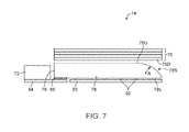
- FIG. 7 is a cross-sectional side view of illustrative display layers and backlight structures showing how a light guide plate may have rounded edges in accordance with an embodiment of the present invention.
- FIG. 8 is a perspective view of an illustrative light guide plate having a rounded edge on one side and a straight edge on an opposing side in accordance with an embodiment of the present invention.
- FIG. 9 is a perspective view of a portion of an illustrative light guide plate having blunt edges such as a chamfered edge in accordance with an embodiment of the present invention.
- FIG. 10 is a perspective view of a portion of an illustrative light guide plate having blunt edges such as a demi bullnose edge in accordance with an embodiment of the present invention.
- FIG. 11 is a perspective view of a portion of an illustrative light guide plate having blunt edges such as a tapered edge in accordance with an embodiment of the present invention.
- FIG. 12 is a perspective view of a portion of an illustrative light guide plate having blunt edges such as a full bullnose edge in accordance with an embodiment of the present invention.
- FIG. 13 is a perspective view of a portion of an illustrative light guide plate having blunt edges such as a beveled edge in accordance with an embodiment of the present invention.
- FIG. 14 is a perspective view of an illustrative light guide plate having alignment features and blunt edges in accordance with an embodiment of the present invention.
- FIG. 15 is a diagram of an illustrative injection molding system that may be used in forming light guide plates having blunt edges in accordance with an embodiment of the present invention.
- FIG. 16 is a diagram of illustrative equipment that may be used to modify edges of a light guide plate in accordance with an embodiment of the present invention.
- FIG. 17 is a diagram of illustrative equipment that may be used to modify edges of a light guide plate in accordance with an embodiment of the present invention.
- FIG. 18 is a diagram showing how a molding tool and a grinding tool may be used in forming a light guide plate having blunt edges and showing how the light guide plate and additional device parts such as a housing are assembled to form a finished electronic device in accordance with an embodiment of the present invention.
- Electronic devices may include displays.
- the displays may be used to display images to a user.
- Illustrative electronic devices that may be provided with displays are shown in FIGS. 1 , 2 , and 3 .
- FIG. 1 shows how electronic device 10 may have the shape of a laptop computer having upper housing 12 A and lower housing 12 B with components such as keyboard 16 and touchpad 18 .
- Device 10 may have hinge structures 20 that allow upper housing 12 A to rotate in directions 22 about rotational axis 24 relative to lower housing 12 B.
- Display 14 may be mounted in upper housing 12 A.
- Upper housing 12 A which may sometimes referred to as a display housing or lid, may be placed in a closed position by rotating upper housing 12 A towards lower housing 12 B about rotational axis 24 .
- FIG. 2 shows how electronic device 10 may be a handheld device such as a cellular telephone, music player, gaming device, navigation unit, or other compact device.
- housing 12 may have opposing front and rear surfaces.
- Display 14 may be mounted on a front face of housing 12 .
- Display 14 may, if desired, have a display cover layer or other exterior layer that includes openings for components such as button 26 . Openings may also be formed in a display cover layer or other display layer to accommodate a speaker port (see, e.g., speaker port 28 of FIG. 2 ).
- FIG. 3 shows how electronic device 10 may be a tablet computer.
- housing 12 may have opposing planar front and rear surfaces.
- Display 14 may be mounted on the front surface of housing 12 .
- display 14 may have a cover layer or other external layer with an opening to accommodate button 26 (as an example).
- FIG. 4 shows an illustrative configuration for electronic device 10 in which device 10 is a computer display or a computer that has been integrated into a computer display.
- housing 12 for device 10 is mounted on a support structure such as stand 27 .
- Display 14 is mounted on a front face of housing 12 .
- electronic device 10 may be a laptop computer, a computer monitor containing an embedded computer, a tablet computer, a cellular telephone, a media player, or other handheld or portable electronic device, a smaller device such as a wrist-watch device, a pendant device, a headphone or earpiece device, or other wearable or miniature device, a television, a computer display that does not contain an embedded computer, a gaming device, a navigation device, an embedded system such as a system in which electronic equipment with a display is mounted in a kiosk or automobile, equipment that implements the functionality of two or more of these devices, or other electronic equipment.
- Housing 12 of device 10 may be formed of materials such as plastic, glass, ceramics, carbon-fiber composites and other fiber-based composites, metal (e.g., machined or cast aluminum, stainless steel, or other metals), other materials, or a combination of these materials.
- Device 10 may be formed using a unibody construction in which most or all of housing 12 is formed from a single structural element (e.g., a piece of machined metal or a piece of molded plastic) or may be formed from multiple housing structures (e.g., outer housing structures that have been mounted to internal frame elements or other internal housing structures).
- Display 14 may be a touch sensitive display that includes a touch sensor or may be insensitive to touch.
- Touch sensors for display 14 may be formed from an array of capacitive touch sensor electrodes, a resistive touch array, touch sensor structures based on acoustic touch, optical touch, or force-based touch technologies, or other suitable touch sensor components.
- Displays for device 10 may, in general, include image pixels formed from light-emitting diodes (LEDs), organic LEDs (OLEDs), plasma cells, electrowetting pixels, electrophoretic pixels, liquid crystal display (LCD) components, or other suitable image pixel structures.
- LEDs light-emitting diodes
- OLEDs organic LEDs
- LCD liquid crystal display
- it may be desirable to use LCD components to form display 14 so configurations for display 14 in which display 14 is a liquid crystal display are sometimes described herein as an example. It may also be desirable to provide displays such as display 14 with backlight structures, so configurations for display 14 that include a backlight unit may sometimes be described herein as an example.
- Other types of display technology may be used in device 10 if desired.
- the use of liquid crystal display structures and backlight structures in device 10 is merely illustrative.
- a display cover layer may cover the surface of display 14 or a display layer such as a color filter layer or other portion of a display may be used as the outermost (or nearly outermost) layer in display 14 .
- a display cover layer or other outer display layer may be formed from a transparent glass sheet, a clear plastic layer, or other transparent member.
- Touch sensor components such as an array of capacitive touch sensor electrodes formed from transparent materials such as indium tin oxide may be formed on the underside of a display cover layer, may be formed on a separate display layer such as a glass or polymer touch sensor substrate, or may be integrated into other display layers (e.g., substrate layers such as a thin-film transistor layer).
- Control circuitry 29 may include storage and processing circuitry for controlling the operation of device 10 .
- Control circuitry 29 may, for example, include storage such as hard disk drive storage, nonvolatile memory (e.g., flash memory or other electrically-programmable-read-only memory configured to form a solid state drive), volatile memory (e.g., static or dynamic random-access-memory), etc.
- Control circuitry 29 may include processing circuitry based on one or more microprocessors, microcontrollers, digital signal processors, baseband processors, power management units, audio codec chips, application specific integrated circuits, etc.
- Control circuitry 29 may be used to run software on device 10 , such as operating system software and application software. Using this software, control circuitry 29 may present information to a user of electronic device 10 on display 14 . When presenting information to a user on display 14 , sensor signals and other information may be used by control circuitry 29 in making adjustments to the strength of backlight illumination that is used for display 14 .
- Input-output circuitry 30 may be used to allow data to be supplied to device 10 and to allow data to be provided from device 10 to external devices.
- Input-output circuitry 30 may include communications circuitry 32 .
- Communications circuitry 32 may include wired communications circuitry for supporting communications using data ports in device 10 .
- Communications circuitry 32 may also include wireless communications circuits (e.g., circuitry for transmitting and receiving wireless radio-frequency signals using antennas).
- Input-output circuitry 30 may also include input-output devices 34 .
- a user can control the operation of device 10 by supplying commands through input-output devices 34 and may receive status information and other output from device 10 using the output resources of input-output devices 34 .
- Input-output devices 34 may include sensors and status indicators 36 such as an ambient light sensor, a proximity sensor, a temperature sensor, a pressure sensor, a magnetic sensor, an accelerometer, and light-emitting diodes and other components for gathering information about the environment in which device 10 is operating and providing information to a user of device 10 about the status of device 10 .
- sensors and status indicators 36 such as an ambient light sensor, a proximity sensor, a temperature sensor, a pressure sensor, a magnetic sensor, an accelerometer, and light-emitting diodes and other components for gathering information about the environment in which device 10 is operating and providing information to a user of device 10 about the status of device 10 .
- Audio components 38 may include speakers and tone generators for presenting sound to a user of device 10 and microphones for gathering user audio input.
- Display 14 may be used to present images for a user such as text, video, and still images.
- Sensors 36 may include a touch sensor array that is formed as one of the layers in display 14 .
- buttons and other input-output components 40 such as touch pad sensors, buttons, joysticks, click wheels, scrolling wheels, touch sensors such as sensors 36 in display 14 , key pads, keyboards, vibrators, cameras, and other input-output components.
- FIG. 6 A cross-sectional side view of an illustrative configuration that may be used for display 14 of device 10 (e.g., for display 14 of the devices of FIG. 1 , FIG. 2 , FIG. 3 , or FIG. 4 or other suitable electronic devices) is shown in FIG. 6 .
- display 14 may include backlight structures such as backlight unit 42 for producing backlight 44 .
- backlight 44 travels outwards (vertically upwards in dimension Z in the orientation of FIG. 6 ) and passes through display pixel structures in display layers 46 . This illuminates any images that are being produced by the display pixels for viewing by a user.
- backlight 44 may illuminate images on display layers 46 that are being viewed by viewer 48 in direction 50 .
- Display layers 46 may be mounted to chassis structures such as a plastic chassis structure and/or a metal chassis structure to form a display module for mounting in housing 12 or display layers 46 may be mounted directly in housing 12 (e.g., by stacking display layers 46 into a recessed portion in housing 12 ). Display layers 46 may form a liquid crystal display or may be used in forming displays of other types.
- display layers 46 may include a liquid crystal layer such a liquid crystal layer 52 .
- Liquid crystal layer 52 may be sandwiched between display layers such as display layers 58 and 56 .
- Layers 56 and 58 may be interposed between lower polarizer layer 60 and upper polarizer layer 54 .
- upper polarizer layer 54 may be attached to an outer cover layer such as cover layer 49 ( FIG. 6 ).
- Layers 58 and 56 may be formed from transparent substrate layers such as clear layers of glass or plastic. Layers 56 and 58 may be layers such as a thin-film transistor layer and/or a color filter layer. Conductive traces, color filter elements, transistors, and other circuits and structures may be formed on the substrates of layers 58 and 56 (e.g., to form a thin-film transistor layer and/or a color filter layer). Touch sensor electrodes may also be incorporated into layers such as layers 58 and 56 and/or touch sensor electrodes may be formed on other substrates. Display layers 46 may sometimes collectively be referred to herein as a “display cell” or a “display unit.”
- layer 58 may be a thin-film transistor layer that includes an array of thin-film transistors and associated electrodes (display pixel electrodes) for applying electric fields to liquid crystal layer 52 and thereby displaying images on display 14 .
- Layer 56 may be a color filter layer that includes an array of color filter elements for providing display 14 with the ability to display color images. If desired, layer 58 may be a color filter layer and layer 56 may be a thin-film transistor layer.
- control circuitry 29 e.g., one or more integrated circuits such as components 68 on printed circuit 66 of FIG. 6
- control circuitry 29 may be used to generate information to be displayed on display 14 (e.g., display data).
- the information to be displayed may be conveyed from circuitry 68 to display driver integrated circuit 62 using a signal path such as a signal path formed from conductive metal traces in flexible printed circuit 64 (as an example).
- Display driver integrated circuit 62 may be mounted on thin-film transistor layer driver ledge 82 or elsewhere in device 10 .
- a flexible printed circuit cable such as flexible printed circuit 64 may be used in routing signals between printed circuit 66 and thin-film transistor layer 58 . If desired, display driver integrated circuit 62 may be mounted on printed circuit 66 or flexible printed circuit 64 .
- Printed circuit 66 may be formed from a rigid printed circuit board (e.g., a layer of fiberglass-filled epoxy) or a flexible printed circuit (e.g., a flexible sheet of polyimide or other flexible polymer layer). However, these examples are merely illustrative. If desired printed circuits 64 and 66 may be formed from a combination of rigid and flexible printed circuit layers (e.g., printed circuit 66 may be formed from a rigid printed circuit board with a layer of flexible printed circuitry that extends from an edge of printed circuit 66 to form flexible printed circuitry 64 that attaches to thin-film transistor layer 58 ).
- Backlight structures 42 may include a backlight light guide plate such as light guide plate 78 .
- Light guide plate 78 may be formed from a transparent material such as clear glass or plastic.
- a light source such as light source 72 may generate light 74 .
- Light source 72 may be, for example, an array of light-emitting diodes.
- Light 74 from light source 72 may be coupled into edge surface 76 of light guide plate 78 and may be distributed laterally in dimensions X and Y throughout light guide plate 78 due to the principal of total internal reflection.
- Light guide plate 78 may include light-scattering features such as pits or bumps or other light-scattering structures. The light-scattering features may be located on an upper surface and/or on an opposing lower surface of light guide plate 78 .
- Light 74 that scatters upwards in direction Z from light guide plate 78 may serve as backlight 44 for display 14 .
- Light 74 that scatters downwards may be reflected back in the upwards direction by reflector 80 .
- Reflector 80 may be formed from a reflective material such as a layer of white plastic or other shiny materials.
- backlight structures 42 may include optical films 70 .
- Optical films 70 may include diffuser layers for helping to homogenize backlight 44 and thereby reduce hotspots, compensation films for enhancing off-axis viewing, and brightness enhancement films (also sometimes referred to as turning films) for collimating backlight 44 .
- Brightness enhancement films also sometimes referred to as turning films
- Optical films 70 may overlap the other structures in backlight unit 42 such as light guide plate 78 and reflector 80 . For example, if light guide plate 78 has a rectangular footprint in the X-Y plane of FIG. 6 , optical films 70 and reflector 80 may have a matching rectangular footprint.
- the layers in a display such as optical film layers may be susceptible to damage.
- conventional light guide plates have sharp edges around the periphery of the light guide plate that can scratch optical film layers such as an adjacent diffuser layer. This type of abrasive contact between sharp edges of the light guide plate and the adjacent optical films can produce dust particles which in turn can damage other optical films in the display.
- light guide plate 78 may have one or more blunt edges.
- a cross-sectional side view of backlight structures 46 in which light guide plate 78 is provided with blunt edges is shown in FIG. 7 .
- light guide plate 78 may be interposed between reflector 80 and optical films 70 .
- a light source such as light source 72 may emit light into edge surface 76 of light guide plate 78 .
- Light-scattering features 92 e.g., pits, bumps, or other light-scattering structures
- Light-scattering features 92 may help scatter light upwards through display layers in display 14 .
- Light-scattering features 92 may be formed on lower surface 78 L (as shown in FIG. 7 ) or may be formed on opposing upper surface 78 U.
- Light source 72 may, for example, be a strip of light-emitting diodes that runs along edge surface 76 of light guide plate 78 .
- Light-emitting diodes 72 may be mounted on a substrate such as substrate 84 .
- Substrate 84 may be formed from a flexible printed circuit substrate material such as polyimide or a sheet of other flexible polymer or may be formed from a rigid printed circuit board material (e.g., fiberglass-filled epoxy material such as FR4).
- Light guide plate 78 may be attached to substrate 84 using adhesive such as adhesive 86 .
- Adhesive 86 may be pressure-sensitive adhesive, light-cured adhesive, liquid adhesive, or other suitable adhesive.
- Light guide plate 78 may have an upper surface such as upper surface 78 U and a lower surface such as lower surface 78 L.
- Upper surface 78 U may be adjacent to optical films 70 (e.g., adjacent to a diffuser layer such as diffuser layer 70 D in optical films 70 ), whereas lower surface 78 L may be adjacent to reflector 80 .
- Upper surface 78 U may have a curved portion such as curved portion 78 S that joins the planar portion of upper surface 78 U with planar lower surface 78 L.
- Curved surface 78 S may, for example, have a radius of curvature R of greater than 10 microns, greater than 50 microns, greater than 100 microns, greater than 500 microns, or less than 500 microns.
- Curved surface 78 S of light guide plate 78 may form a blunt edge that minimizes abrasive contact between light guide plate 78 and optical films 70 .
- light guide plate 78 may have a combination of blunt edges such as blunt edge 78 S and straight edges such as straight edge 76 .
- blunt edge 78 S has a rectangular shape with four edges. One, two, three, or all four of these edges may be blunt edges formed from curved or beveled surfaces.
- edge 78 S is a blunt edge formed from a curved surface.
- Opposing edge 76 is a straight edge.
- blunt edge 78 S may extend along an entire side of light guide plate 78 from corner C 1 to corner C 2 or may extend only partially along a side of light guide plate 78 .
- Edge 76 may be formed from a flat vertical sidewall surface that extends along an entire side of light guide plate 78 or edge 76 may be formed from portions with curved surfaces and portions with vertical sidewall surfaces. In configurations where edge 76 is used as a light coupling edge for receiving light from light source 72 ( FIG. 7 ), edge 76 may have light coupling regions with surface variations that facilitate light coupling. For example, edge 76 may have light coupling regions that include vertically extending corrugations or other surface textures (e.g., curved surfaces, scalloped surfaces, sawtooth surfaces, angled surfaces, a combination of these surfaces, etc.).
- edge 76 may have vertical sidewall surfaces (e.g., sidewall surfaces that are oriented perpendicularly to upper surface 78 U and lower surface 78 L of light guide plate 78 ) interspersed among other surface regions (e.g., curved edge segments, beveled edge segments, other blunt edge segments, etc.).
- vertical sidewall surfaces e.g., sidewall surfaces that are oriented perpendicularly to upper surface 78 U and lower surface 78 L of light guide plate 78
- other surface regions e.g., curved edge segments, beveled edge segments, other blunt edge segments, etc.
- a “blunt” edge may refer to an edge formed from a curved surface (e.g., a surface having a radius of curvature R of greater than 50 microns) or may refer to an edge with an interior angle of greater than 90 degrees, for example.
- a “straight” edge may refer to an edge with an interior angle of approximately 90 degrees, for example.
- Edge 76 in the example of FIG. 7 is defined by an interior angle of approximately 90 degrees and is sometimes referred to as a flat or square edge.
- light guide plate 78 may have one blunt edge and three straight edges, two blunt edges and two straight edges, three blunt edges and one straight edge, the entire periphery of light guide plate 78 may have blunt edges, etc.
- the example of FIG. 8 is merely illustrative.
- blunt edges such as edge 78 S of light guide plate 78 .
- Illustrative examples of different surface geometries that may be used to form blunt edges such as edge 78 S are shown in FIGS. 9-13 .
- blunt edge 78 S of light guide plate 78 is formed from a chamfered surface (sometimes referred to as a beveled surface).
- a series of planar surfaces 88 that are angled with respect to one another may join upper surface 78 U with lower surface 78 L of light guide plate 78 .
- three planar surfaces 88 are used to join upper surface 78 U with lower surface 78 L of light guide plate 78 . This is, however, merely illustrative. If desired, there may be more than three surfaces 88 or less than three surfaces 88 joining upper surface 78 U with lower surface 78 L.
- a single planar surface 88 (e.g., angled with respect to planar surface 78 U by an interior angle of greater than 90 degrees) may be used to form a beveled edge that joins upper surface 78 U with lower surface 78 L.
- blunt edge 78 S of light guide plate 78 is formed from a rounded surface.
- This type of edge is sometimes referred to as a half bullnose, a demi bullnose, or eased edge.
- a smooth curved surface may join planar upper surface 78 U of light guide plate 78 with planar lower surface 78 L of light guide plate 78 .
- Curved surface 78 S may, for example, take the place of a planar sidewall at an edge of light guide plate 78 .
- blunt edge 78 S of light guide plate 78 is formed from a curved surface that forms a tapered edge.
- the central portion of light guide plate 78 may have a first thickness T 1 in between upper surface 78 U and lower surface 78 L.
- the edge portion at edge 78 S may have a second thickness T 2 less than thickness T 1 .
- the curved surface of tapered edge 78 S of FIG. 11 may transition gradually from the central portion to the edge portion such that abrasive contact between light guide plate 78 and adjacent optical films 70 ( FIG. 7 ) is minimized.
- blunt edge 78 S of light guide plate 78 is formed from a curved surface that forms a full bullnose edge.
- edge 78 S has a c-shaped cross section in which upper surface 78 U and lower surface 78 L are joined by a smooth c-shaped curved surface 78 S.
- blunt edge 78 S of light guide plate 78 is formed from a beveled edge (e.g., a half-beveled edge, a quarter-beveled edge, etc.).
- the example of FIG. 13 is similar to that of FIG. 9 except that the example of FIG. 13 includes a vertical side wall portion 99 .
- light guide plate 78 may have alignment features that help align and secure light guide plate 78 within housing 12 of device 10 .
- light guide plate 78 may have alignment structures 78 E that protrude out laterally from light guide plate 78 .
- Alignment structures 78 E (sometimes referred to as protrusions or tabs) may be received by corresponding alignment structures in housing 12 of device 10 or in other structures surrounding display 14 .
- light guide plate alignment structures 78 E may have engagement features such as openings 79 for receiving corresponding engagement features such as posts or protrusions to hold light guide plate 78 in place within device 10 .
- FIG. 14 The example of FIG. 14 in which light guide plate 78 has two alignment structures 78 E formed on a single edge of light guide plate 78 is merely illustrative. If desired, there may be one or more alignment structures 78 E on one, two, three, or all four sides of light guide plate 78 .
- light guide plate alignment structures 78 E may have blunt edges 78 S to minimize abrasive contact between alignment structures 78 E and adjacent optical films 70 ( FIG. 7 ). Blunt edges of alignment structures 78 E may take the form of any of the illustrative blunt edges shown in FIGS. 9-13 .
- injection molding system 200 may include a mold such as mold 202 .
- Mold 202 may include a mold cavity 202 C.
- Mold cavity 202 C may have the negative shape of light guide plate 78 with blunt edge 78 S such that, when filled with plastic, the resulting part has the shape of light guide plate 78 with blunt edge 78 S.
- upper mold 202 C has curved surface 202 S that helps form blunt edges 78 S of light guide plate 78 .
- a shot of pelletized thermoplastic material (e.g., thermoplastic granules or “resin”) may be added to a hopper such as hopper 282 .
- the material may be gravity fed into a screw-type plunger such as plunger 284 .
- the heat generated by heating unit 286 and the rotation of the screw in plunger 284 may result in elevated temperatures and a shearing action on the thermoplastic pellets that causes the pellets to melt into molten plastic.
- Screw rotation in plunger 284 may push the molten plastic towards nozzle 288 and into mold cavity 202 C.
- mold 202 When mold 202 has been completely filled, the molten plastic may be cooled. When the plastic has solidified, mold 202 may be removed (e.g., mold 202 may be opened by separating upper portion 202 U from lower portion 202 L along line 244 ).
- the plastic that solidifies within cavity 202 C may form light guide plate 78 with blunt edge 78 S.
- additional processing operations may be performed to light guide plate 78 .
- the edges of light guide plate 78 such as edge 78 S (and other edges of light guide plate 78 , if desired) may be grinded and/or polished.
- Illustrative equipment that may be used to modify edge surfaces such as edge surface 78 S of light guide plate 78 is shown in FIGS. 16 and 17 .
- equipment 234 may include computer-controlled positioner 236 and machining tool head 238 A.
- Head 238 A has a surface profile that is configured to grind and/or polish edge surface 78 S to form a rounded surface with a c-shaped cross section (e.g., a full bullnose edge).
- positioner 236 rotates machining tool head 238 A (e.g., using a motor) about axis 240 while moving tool 238 A along edge 78 S of light guide plate 78 , thereby machining edge surface 78 S of light guide plate 78 into a desired shape.
- machining tool head 238 A e.g., using a motor
- computer-controlled positioner 235 may be used to move light guide plate 78 during edge polishing operations while equipment 234 remains in a fixed position.
- equipment 234 includes machining tool head 238 B.
- Head 238 B has a surface profile that is configured to grind and/or polish edge surface 78 S to form a partially rounded surface (e.g., a demi bullnose edge or a half bullnose edge having a curved surface portion and a planar surface portion).
- equipment 234 may be used to modify (e.g., grind and/or polish) all four edges of light guide plate 78 or equipment 234 may be used to modify one or more of the edges of light guide plate 78 .
- the machining tool head that is used to modify a given edge of light guide plate 78 may have a surface profile corresponding to the desired surface profile of that edge.
- a combination of machining tool heads having different surface profiles may be used to treat the four edges of light guide plate 78 (e.g., machining tool heads with flat surface profiles, machining tool heads with curved surface profiles, etc.).
- FIG. 18 A flow chart of illustrative steps involved in forming light guide plate 78 using the injection molding tool of FIG. 15 and equipment 234 of FIGS. 16 and 17 is shown in FIG. 18 .
- equipment such as molding tool 200 may receive polymer material 300 (e.g., a clear resin such as polymethyl methacrylate resin or other acrylic resin, a polycarbonate resin, etc.). Molding tool 200 may be used in molding polymer 300 into light guide plate 78 having blunt edge 78 S. In some configurations, the resulting part formed by molding tool 200 may have a tail portion such as tail portion 78 T at edge 78 S.
- Light guide plate 78 may taper from a first thickness T 1 ′ at the central portion of light guide plate 78 to a second thickness T 2 ′ at tail portion 78 T of light guide plate 78 .
- the blunt edge formed by curved surface 78 S may minimize abrasive contact with and scratches on adjacent optical films 70 in display 14 of device 10 .
- light guide plate 78 may be grinded and polished using a grinding tool such as grinding tool 234 .
- Grinding tool 234 may be used to grind down and thereby remove all or a portion of tail portion 78 T at edge 78 S.
- Grinding tool 234 may also be used in shaping and polishing one or more edges of light guide plate 78 to form smooth edges. For example, any plastic that seeps between upper mold 202 U and lower mold 202 L (e.g., at interface 244 ) during the injection molding process (sometimes referred to as flash or burrs) may be removed during the grinding/polishing step of FIG. 18 . If desired, all four edges of light guide plate 78 may be polished using grinding tool 234 .
- light guide plate 78 , other layers of display 14 , housing 12 , and other parts in electronic device 10 may be assembled using assembly equipment 304 , thereby forming finished electronic device 10 .
- This may include, for example, attaching light guide plate 78 to light-emitting diode substrate 84 of FIG. 7 .
Abstract
Description
Claims (18)
Priority Applications (4)
| Application Number | Priority Date | Filing Date | Title |
|---|---|---|---|
| US14/049,114 US9239422B2 (en) | 2012-12-20 | 2013-10-08 | Light guide plate with blunt edges |
| TW102143311A TWI622838B (en) | 2012-12-20 | 2013-11-27 | Light guide plate with blunt edges |
| CN201310664776.9A CN103883939A (en) | 2012-12-20 | 2013-12-10 | Light guide plate with blunt edges |
| KR1020130153366A KR101567155B1 (en) | 2012-12-20 | 2013-12-10 | Light guide plate with blunt edges |
Applications Claiming Priority (2)
| Application Number | Priority Date | Filing Date | Title |
|---|---|---|---|
| US201261739931P | 2012-12-20 | 2012-12-20 | |
| US14/049,114 US9239422B2 (en) | 2012-12-20 | 2013-10-08 | Light guide plate with blunt edges |
Publications (2)
| Publication Number | Publication Date |
|---|---|
| US20140176868A1 US20140176868A1 (en) | 2014-06-26 |
| US9239422B2 true US9239422B2 (en) | 2016-01-19 |
Family
ID=50974257
Family Applications (1)
| Application Number | Title | Priority Date | Filing Date |
|---|---|---|---|
| US14/049,114 Expired - Fee Related US9239422B2 (en) | 2012-12-20 | 2013-10-08 | Light guide plate with blunt edges |
Country Status (2)
| Country | Link |
|---|---|
| US (1) | US9239422B2 (en) |
| TW (1) | TWI622838B (en) |
Families Citing this family (8)
| Publication number | Priority date | Publication date | Assignee | Title |
|---|---|---|---|---|
| JP6512827B2 (en) * | 2015-01-07 | 2019-05-15 | 三菱電機株式会社 | Liquid crystal display device and method of manufacturing the same |
| TWI581024B (en) * | 2015-07-14 | 2017-05-01 | 茂林光電科技股份有限公司 | A method of manufacturing a thin trumpet-shaped light guide plate, and the equipment |
| WO2017022622A1 (en) * | 2015-07-31 | 2017-02-09 | 富士フイルム株式会社 | Laminated film |
| US20170057134A1 (en) * | 2015-09-01 | 2017-03-02 | Proradiant Opto. Co., Ltd. | Method for manufacturing an optical element |
| KR102608241B1 (en) * | 2016-10-26 | 2023-11-30 | 삼성디스플레이 주식회사 | Display device |
| KR102600982B1 (en) * | 2016-10-28 | 2023-11-13 | 삼성전자주식회사 | Display apparatus |
| TW201901209A (en) * | 2017-05-03 | 2019-01-01 | 美商康寧公司 | a light guide comprising an equiangular spiral curvature and an element comprising the light guide |
| TWI820707B (en) * | 2022-03-11 | 2023-11-01 | 瑞儀光電股份有限公司 | Backlight module and display device |
Citations (56)
| Publication number | Priority date | Publication date | Assignee | Title |
|---|---|---|---|---|
| US4812830A (en) | 1986-12-08 | 1989-03-14 | Digital Electronics Corporation | Touch panel display assembly |
| JPH05142538A (en) | 1991-11-21 | 1993-06-11 | Hitachi Ltd | Liquid crystal display device |
| US5422751A (en) | 1992-10-14 | 1995-06-06 | Apple Computer, Inc. | Liquid crystal display assembly employing front bezel, frame holding liquid crystal cell attached to bezel, and light source and back plate attached to bezel |
| US5483261A (en) | 1992-02-14 | 1996-01-09 | Itu Research, Inc. | Graphical input controller and method with rear screen image detection |
| US5488204A (en) | 1992-06-08 | 1996-01-30 | Synaptics, Incorporated | Paintbrush stylus for capacitive touch sensor pad |
| US5825352A (en) | 1996-01-04 | 1998-10-20 | Logitech, Inc. | Multiple fingers contact sensing method for emulating mouse buttons and mouse operations on a touch sensor pad |
| US5835079A (en) | 1996-06-13 | 1998-11-10 | International Business Machines Corporation | Virtual pointing device for touchscreens |
| US5880411A (en) | 1992-06-08 | 1999-03-09 | Synaptics, Incorporated | Object position detector with edge motion feature and gesture recognition |
| US5988827A (en) | 1996-07-11 | 1999-11-23 | Samsung Electronics Co., Ltd. | Display devices having rounded corner backlight unit |
| US6061231A (en) | 1993-09-01 | 2000-05-09 | Ncr Corporation | Computer display assembly |
| US6071616A (en) | 1996-12-05 | 2000-06-06 | Texas Instruments Incorporated | Opaque low reflecting coating aperture on glass |
| US6188391B1 (en) | 1998-07-09 | 2001-02-13 | Synaptics, Inc. | Two-layer capacitive touchpad and method of making same |
| US6280885B1 (en) | 1999-08-11 | 2001-08-28 | Dupont Photomasks, Inc. | Dust cover comprising anti-reflective coating |
| US6310610B1 (en) | 1997-12-04 | 2001-10-30 | Nortel Networks Limited | Intelligent touch display |
| US6323846B1 (en) | 1998-01-26 | 2001-11-27 | University Of Delaware | Method and apparatus for integrating manual input |
| US6369866B1 (en) | 1998-02-19 | 2002-04-09 | Sanyo Electric Co., Ltd. | Liquid crystal display having a light collecting mechanism with a light transmitter optically connected to the light guide plate and light collector for collecting ambient light |
| US6419372B1 (en) | 2000-09-08 | 2002-07-16 | Rockwell Collins, Inc. | Compact optical wave-guide system for LED backlighting liquid crystal displays |
| US20020114152A1 (en) | 2001-02-21 | 2002-08-22 | Kouzou Fujino | Light-guide plate, area light source apparatus, and image reading apparatus |
| US20020145762A1 (en) | 2001-04-05 | 2002-10-10 | Chuan-Yu Hsu | Optical chassis pasted with plating film reflection thin plates |
| US20030164894A1 (en) | 2001-04-05 | 2003-09-04 | Chuan-Yu Hsu | Optical chassis of plating film reflection and its manufacturing procedure |
| US6690387B2 (en) | 2001-12-28 | 2004-02-10 | Koninklijke Philips Electronics N.V. | Touch-screen image scrolling system and method |
| JP2004061622A (en) | 2002-07-25 | 2004-02-26 | Minolta Co Ltd | Light guide element for illumination |
| US6738118B2 (en) | 2001-03-17 | 2004-05-18 | Samsung Electronics Co., Ltd. | Liquid crystal display device |
| US20040114345A1 (en) * | 2002-12-12 | 2004-06-17 | Dong-Hoon Kim | Light guide plate with stepped edge and display device having the same |
| US6753937B2 (en) | 2000-11-27 | 2004-06-22 | Asulab S.A. | Reflective liquid crystal display device having a black absorbent layer |
| US6753843B2 (en) | 2001-11-30 | 2004-06-22 | Chi Mei Optoelectronics Corp. | Frame for use in backlight module |
| US20060026521A1 (en) | 2004-07-30 | 2006-02-02 | Apple Computer, Inc. | Gestures for touch sensitive input devices |
| US7015894B2 (en) | 2001-09-28 | 2006-03-21 | Ricoh Company, Ltd. | Information input and output system, method, storage medium, and carrier wave |
| US7071927B2 (en) | 1999-11-17 | 2006-07-04 | L-3 Communications Corporation | Resistive touch panel using removable, tensioned top layer |
| US20060158511A1 (en) | 2003-07-10 | 2006-07-20 | Ocuity Limited | Alignment of elements of a display apparatus |
| US20060164863A1 (en) | 2005-01-26 | 2006-07-27 | Chia-Yin Chang | Light guide plate for uniformly scattering lights from point light source |
| US20060197753A1 (en) | 2005-03-04 | 2006-09-07 | Hotelling Steven P | Multi-functional hand-held device |
| KR20060104511A (en) | 2005-03-30 | 2006-10-09 | 엘지.필립스 엘시디 주식회사 | Liquid crystal display device module |
| US20070030420A1 (en) | 2005-08-08 | 2007-02-08 | Samsung Electronics Co., Ltd. | Liquid crystal display and method of assembling the same |
| US7195392B2 (en) | 2004-01-29 | 2007-03-27 | A U Optronics Corporation | Backlight module with an impact damping design |
| US20070127261A1 (en) | 2005-12-02 | 2007-06-07 | Samsung Electro-Mechanics Co., Ltd. | LED backlight device |
| CN1987596A (en) | 2005-12-22 | 2007-06-27 | 群康科技(深圳)有限公司 | Back light module and liquid crystal display device |
| JP2008103301A (en) | 2006-09-21 | 2008-05-01 | Sharp Corp | Backlight device |
| US20080198627A1 (en) | 2007-02-20 | 2008-08-21 | Mitsubishi Electric Corporation | Planar light source device and display device |
| JP2008198540A (en) | 2007-02-15 | 2008-08-28 | Epson Imaging Devices Corp | Optical sheet, backlight device using optical sheet, and liquid crystal display |
| US20080204624A1 (en) | 2007-02-28 | 2008-08-28 | Innocom Technology (Shenzhen) Co., Ltd. | Liquid crystal display with accommodating frame having reflecting portion and light absorbing portion |
| US20090185098A1 (en) | 2008-01-17 | 2009-07-23 | Kyu-Han Bae | Dual liquid crystal display (LCD) |
| US7663607B2 (en) | 2004-05-06 | 2010-02-16 | Apple Inc. | Multipoint touchscreen |
| TWM376786U (en) | 2009-10-16 | 2010-03-21 | Synergy Engineering Co Ltd | Light guide device and forming equipment |
| US7948573B2 (en) | 2006-08-10 | 2011-05-24 | Samsung Electronics Co., Ltd. | Back-light assembly and liquid crystal display including the same |
| US20110255023A1 (en) | 2010-04-15 | 2011-10-20 | Doyle David A | Electronic device display structures with controlled chassis reflections |
| US8051980B2 (en) | 2007-11-02 | 2011-11-08 | Hong Fu Jin Precision Industry (Shenzhen) Co., Ltd. | Protective sleeve for portable electronic devices |
| US20110285661A1 (en) | 2010-05-18 | 2011-11-24 | Steven Porter Hotelling | Periphery Conductive Element for Touch Screen |
| US20120063167A1 (en) | 2010-09-03 | 2012-03-15 | Omron Corporation | Surface light source device and frame used therein |
| US20120214417A1 (en) | 2011-02-23 | 2012-08-23 | Sungho Woo | Systems for remotely waking up application processor of mobile device |
| KR20120116290A (en) | 2011-04-12 | 2012-10-22 | 엘지디스플레이 주식회사 | Liquid crystal display device |
| KR20120125875A (en) | 2011-05-09 | 2012-11-19 | 박철 | Methode of manufacturing light guide plate and the light guide plate |
| US20120327324A1 (en) | 2011-06-23 | 2012-12-27 | Apple Inc. | Coated chassis for liquid crystal display |
| US20130051076A1 (en) * | 2011-08-25 | 2013-02-28 | Hayashi Engineering Inc. | Planar lighting device |
| US20130063978A1 (en) | 2011-09-09 | 2013-03-14 | Shawn R. Gettemy | Chassis for Display Backlight |
| US8558977B2 (en) | 2009-09-11 | 2013-10-15 | Apple Inc. | Electronic device display structures with alignment features |
-
2013
- 2013-10-08 US US14/049,114 patent/US9239422B2/en not_active Expired - Fee Related
- 2013-11-27 TW TW102143311A patent/TWI622838B/en active
Patent Citations (63)
| Publication number | Priority date | Publication date | Assignee | Title |
|---|---|---|---|---|
| US4812830A (en) | 1986-12-08 | 1989-03-14 | Digital Electronics Corporation | Touch panel display assembly |
| JPH05142538A (en) | 1991-11-21 | 1993-06-11 | Hitachi Ltd | Liquid crystal display device |
| US5483261A (en) | 1992-02-14 | 1996-01-09 | Itu Research, Inc. | Graphical input controller and method with rear screen image detection |
| US5488204A (en) | 1992-06-08 | 1996-01-30 | Synaptics, Incorporated | Paintbrush stylus for capacitive touch sensor pad |
| US5880411A (en) | 1992-06-08 | 1999-03-09 | Synaptics, Incorporated | Object position detector with edge motion feature and gesture recognition |
| US5422751A (en) | 1992-10-14 | 1995-06-06 | Apple Computer, Inc. | Liquid crystal display assembly employing front bezel, frame holding liquid crystal cell attached to bezel, and light source and back plate attached to bezel |
| US6061231A (en) | 1993-09-01 | 2000-05-09 | Ncr Corporation | Computer display assembly |
| US5825352A (en) | 1996-01-04 | 1998-10-20 | Logitech, Inc. | Multiple fingers contact sensing method for emulating mouse buttons and mouse operations on a touch sensor pad |
| US5835079A (en) | 1996-06-13 | 1998-11-10 | International Business Machines Corporation | Virtual pointing device for touchscreens |
| US5988827A (en) | 1996-07-11 | 1999-11-23 | Samsung Electronics Co., Ltd. | Display devices having rounded corner backlight unit |
| US6071616A (en) | 1996-12-05 | 2000-06-06 | Texas Instruments Incorporated | Opaque low reflecting coating aperture on glass |
| US6310610B1 (en) | 1997-12-04 | 2001-10-30 | Nortel Networks Limited | Intelligent touch display |
| US6323846B1 (en) | 1998-01-26 | 2001-11-27 | University Of Delaware | Method and apparatus for integrating manual input |
| US6369866B1 (en) | 1998-02-19 | 2002-04-09 | Sanyo Electric Co., Ltd. | Liquid crystal display having a light collecting mechanism with a light transmitter optically connected to the light guide plate and light collector for collecting ambient light |
| TWI238910B (en) | 1998-02-19 | 2005-09-01 | Sanyo Electric Co | Liquid crystal display device with a light collecting device |
| US6188391B1 (en) | 1998-07-09 | 2001-02-13 | Synaptics, Inc. | Two-layer capacitive touchpad and method of making same |
| US6280885B1 (en) | 1999-08-11 | 2001-08-28 | Dupont Photomasks, Inc. | Dust cover comprising anti-reflective coating |
| US7071927B2 (en) | 1999-11-17 | 2006-07-04 | L-3 Communications Corporation | Resistive touch panel using removable, tensioned top layer |
| US6419372B1 (en) | 2000-09-08 | 2002-07-16 | Rockwell Collins, Inc. | Compact optical wave-guide system for LED backlighting liquid crystal displays |
| US6753937B2 (en) | 2000-11-27 | 2004-06-22 | Asulab S.A. | Reflective liquid crystal display device having a black absorbent layer |
| US20020114152A1 (en) | 2001-02-21 | 2002-08-22 | Kouzou Fujino | Light-guide plate, area light source apparatus, and image reading apparatus |
| US6738118B2 (en) | 2001-03-17 | 2004-05-18 | Samsung Electronics Co., Ltd. | Liquid crystal display device |
| US20020145762A1 (en) | 2001-04-05 | 2002-10-10 | Chuan-Yu Hsu | Optical chassis pasted with plating film reflection thin plates |
| US20030164894A1 (en) | 2001-04-05 | 2003-09-04 | Chuan-Yu Hsu | Optical chassis of plating film reflection and its manufacturing procedure |
| US7015894B2 (en) | 2001-09-28 | 2006-03-21 | Ricoh Company, Ltd. | Information input and output system, method, storage medium, and carrier wave |
| US6753843B2 (en) | 2001-11-30 | 2004-06-22 | Chi Mei Optoelectronics Corp. | Frame for use in backlight module |
| US7184064B2 (en) | 2001-12-28 | 2007-02-27 | Koninklijke Philips Electronics N.V. | Touch-screen image scrolling system and method |
| US6690387B2 (en) | 2001-12-28 | 2004-02-10 | Koninklijke Philips Electronics N.V. | Touch-screen image scrolling system and method |
| JP2004061622A (en) | 2002-07-25 | 2004-02-26 | Minolta Co Ltd | Light guide element for illumination |
| US7077554B2 (en) | 2002-12-12 | 2006-07-18 | Samsung Electronics Co., Ltd. | Light guide plate with stepped edge and display device having the same |
| US20040114345A1 (en) * | 2002-12-12 | 2004-06-17 | Dong-Hoon Kim | Light guide plate with stepped edge and display device having the same |
| US20060158511A1 (en) | 2003-07-10 | 2006-07-20 | Ocuity Limited | Alignment of elements of a display apparatus |
| US7195392B2 (en) | 2004-01-29 | 2007-03-27 | A U Optronics Corporation | Backlight module with an impact damping design |
| US7663607B2 (en) | 2004-05-06 | 2010-02-16 | Apple Inc. | Multipoint touchscreen |
| US20060026521A1 (en) | 2004-07-30 | 2006-02-02 | Apple Computer, Inc. | Gestures for touch sensitive input devices |
| US20060164863A1 (en) | 2005-01-26 | 2006-07-27 | Chia-Yin Chang | Light guide plate for uniformly scattering lights from point light source |
| US20060197753A1 (en) | 2005-03-04 | 2006-09-07 | Hotelling Steven P | Multi-functional hand-held device |
| KR20060104511A (en) | 2005-03-30 | 2006-10-09 | 엘지.필립스 엘시디 주식회사 | Liquid crystal display device module |
| US20070030420A1 (en) | 2005-08-08 | 2007-02-08 | Samsung Electronics Co., Ltd. | Liquid crystal display and method of assembling the same |
| US20070127261A1 (en) | 2005-12-02 | 2007-06-07 | Samsung Electro-Mechanics Co., Ltd. | LED backlight device |
| CN1987596A (en) | 2005-12-22 | 2007-06-27 | 群康科技(深圳)有限公司 | Back light module and liquid crystal display device |
| US7948573B2 (en) | 2006-08-10 | 2011-05-24 | Samsung Electronics Co., Ltd. | Back-light assembly and liquid crystal display including the same |
| JP2008103301A (en) | 2006-09-21 | 2008-05-01 | Sharp Corp | Backlight device |
| JP2008198540A (en) | 2007-02-15 | 2008-08-28 | Epson Imaging Devices Corp | Optical sheet, backlight device using optical sheet, and liquid crystal display |
| US20080198627A1 (en) | 2007-02-20 | 2008-08-21 | Mitsubishi Electric Corporation | Planar light source device and display device |
| US7819572B2 (en) | 2007-02-20 | 2010-10-26 | Mitsubishi Electric Corporation | Planar light source device and display device |
| US20080204624A1 (en) | 2007-02-28 | 2008-08-28 | Innocom Technology (Shenzhen) Co., Ltd. | Liquid crystal display with accommodating frame having reflecting portion and light absorbing portion |
| US8031290B2 (en) | 2007-02-28 | 2011-10-04 | Innocom Technology (Shenzhen) Co., Ltd. | Liquid crystal display with accommodating frame having reflecting portion and light absorbing portion |
| US8051980B2 (en) | 2007-11-02 | 2011-11-08 | Hong Fu Jin Precision Industry (Shenzhen) Co., Ltd. | Protective sleeve for portable electronic devices |
| US20090185098A1 (en) | 2008-01-17 | 2009-07-23 | Kyu-Han Bae | Dual liquid crystal display (LCD) |
| US8558977B2 (en) | 2009-09-11 | 2013-10-15 | Apple Inc. | Electronic device display structures with alignment features |
| TWM376786U (en) | 2009-10-16 | 2010-03-21 | Synergy Engineering Co Ltd | Light guide device and forming equipment |
| US8154680B2 (en) | 2010-04-15 | 2012-04-10 | Apple Inc. | Electronic device display structures with controlled chassis reflections |
| US8390759B2 (en) | 2010-04-15 | 2013-03-05 | Apple Inc. | Electronic device display structures with controlled chassis reflections |
| US20110255023A1 (en) | 2010-04-15 | 2011-10-20 | Doyle David A | Electronic device display structures with controlled chassis reflections |
| US20110285661A1 (en) | 2010-05-18 | 2011-11-24 | Steven Porter Hotelling | Periphery Conductive Element for Touch Screen |
| US20120063167A1 (en) | 2010-09-03 | 2012-03-15 | Omron Corporation | Surface light source device and frame used therein |
| US20120214417A1 (en) | 2011-02-23 | 2012-08-23 | Sungho Woo | Systems for remotely waking up application processor of mobile device |
| KR20120116290A (en) | 2011-04-12 | 2012-10-22 | 엘지디스플레이 주식회사 | Liquid crystal display device |
| KR20120125875A (en) | 2011-05-09 | 2012-11-19 | 박철 | Methode of manufacturing light guide plate and the light guide plate |
| US20120327324A1 (en) | 2011-06-23 | 2012-12-27 | Apple Inc. | Coated chassis for liquid crystal display |
| US20130051076A1 (en) * | 2011-08-25 | 2013-02-28 | Hayashi Engineering Inc. | Planar lighting device |
| US20130063978A1 (en) | 2011-09-09 | 2013-03-14 | Shawn R. Gettemy | Chassis for Display Backlight |
Also Published As
| Publication number | Publication date |
|---|---|
| US20140176868A1 (en) | 2014-06-26 |
| TW201426130A (en) | 2014-07-01 |
| TWI622838B (en) | 2018-05-01 |
Similar Documents
| Publication | Publication Date | Title |
|---|---|---|
| US11626578B2 (en) | Borderless display with light-bending structures | |
| US9239422B2 (en) | Light guide plate with blunt edges | |
| US11573603B2 (en) | Multiple-element light-bending structures for minimizing display borders | |
| US11715810B2 (en) | Displays with camera window openings | |
| US9997578B2 (en) | Displays with reduced driver circuit ledges | |
| US20170026553A1 (en) | Displays With Camera Window Openings | |
| US10061158B2 (en) | Light guide plate with integrated reflector for display backlight | |
| US9116267B2 (en) | Backlight structures and assemblies for electronic device displays | |
| US9835786B2 (en) | Display backlight with diffractive and refractive light scattering structures | |
| US9618689B2 (en) | Electronic devices with displays having attached optical films | |
| US9036109B2 (en) | Electronic device with thermally matched light guide plate | |
| US9103512B2 (en) | Electronic device with display backlight alignment structures | |
| KR101567155B1 (en) | Light guide plate with blunt edges | |
| US9304338B2 (en) | Methods for assembling display structures | |
| US20140085576A1 (en) | Light Guide Plates and Optical Films with Mating Alignment Features | |
| US9140925B2 (en) | Display with reduced border |
Legal Events
| Date | Code | Title | Description |
|---|---|---|---|
| AS | Assignment |
Owner name: APPLE INC., CALIFORNIA Free format text: ASSIGNMENT OF ASSIGNORS INTEREST;ASSIGNORS:ZHU, XINYU;CHIU, PO-WEN;QI, JUN;REEL/FRAME:031370/0867 Effective date: 20131007 |
|
| FEPP | Fee payment procedure |
Free format text: PAYOR NUMBER ASSIGNED (ORIGINAL EVENT CODE: ASPN); ENTITY STATUS OF PATENT OWNER: LARGE ENTITY |
|
| ZAAA | Notice of allowance and fees due |
Free format text: ORIGINAL CODE: NOA |
|
| ZAAB | Notice of allowance mailed |
Free format text: ORIGINAL CODE: MN/=. |
|
| ZAAA | Notice of allowance and fees due |
Free format text: ORIGINAL CODE: NOA |
|
| STCF | Information on status: patent grant |
Free format text: PATENTED CASE |
|
| MAFP | Maintenance fee payment |
Free format text: PAYMENT OF MAINTENANCE FEE, 4TH YEAR, LARGE ENTITY (ORIGINAL EVENT CODE: M1551); ENTITY STATUS OF PATENT OWNER: LARGE ENTITY Year of fee payment: 4 |
|
| FEPP | Fee payment procedure |
Free format text: MAINTENANCE FEE REMINDER MAILED (ORIGINAL EVENT CODE: REM.); ENTITY STATUS OF PATENT OWNER: LARGE ENTITY |
|
| LAPS | Lapse for failure to pay maintenance fees |
Free format text: PATENT EXPIRED FOR FAILURE TO PAY MAINTENANCE FEES (ORIGINAL EVENT CODE: EXP.); ENTITY STATUS OF PATENT OWNER: LARGE ENTITY |
|
| STCH | Information on status: patent discontinuation |
Free format text: PATENT EXPIRED DUE TO NONPAYMENT OF MAINTENANCE FEES UNDER 37 CFR 1.362 |
|
| FP | Lapsed due to failure to pay maintenance fee |
Effective date: 20240119 |