US9264062B1 - Digital-to-analog converter circuit - Google Patents
Digital-to-analog converter circuit Download PDFInfo
- Publication number
- US9264062B1 US9264062B1 US14/644,941 US201514644941A US9264062B1 US 9264062 B1 US9264062 B1 US 9264062B1 US 201514644941 A US201514644941 A US 201514644941A US 9264062 B1 US9264062 B1 US 9264062B1
- Authority
- US
- United States
- Prior art keywords
- digital
- analog converter
- current
- sub
- currents
- Prior art date
- Legal status (The legal status is an assumption and is not a legal conclusion. Google has not performed a legal analysis and makes no representation as to the accuracy of the status listed.)
- Active
Links
- 230000005540 biological transmission Effects 0.000 claims description 2
- MSFQEZBRFPAFEX-UHFFFAOYSA-N 4-methoxybenzenesulfonamide Chemical compound COC1=CC=C(S(N)(=O)=O)C=C1 MSFQEZBRFPAFEX-UHFFFAOYSA-N 0.000 description 93
- 230000007704 transition Effects 0.000 description 35
- 238000000034 method Methods 0.000 description 9
- 238000010586 diagram Methods 0.000 description 8
- 229920005994 diacetyl cellulose Polymers 0.000 description 5
- 230000004048 modification Effects 0.000 description 4
- 238000012986 modification Methods 0.000 description 4
- 238000012545 processing Methods 0.000 description 4
- 230000008901 benefit Effects 0.000 description 3
- 239000003990 capacitor Substances 0.000 description 3
- 238000005516 engineering process Methods 0.000 description 3
- 230000004075 alteration Effects 0.000 description 1
- 230000001174 ascending effect Effects 0.000 description 1
- 238000004364 calculation method Methods 0.000 description 1
- 230000008859 change Effects 0.000 description 1
- 238000006243 chemical reaction Methods 0.000 description 1
- 239000000470 constituent Substances 0.000 description 1
- 238000007796 conventional method Methods 0.000 description 1
- 230000001419 dependent effect Effects 0.000 description 1
- 230000009977 dual effect Effects 0.000 description 1
- 238000004519 manufacturing process Methods 0.000 description 1
- 239000000203 mixture Substances 0.000 description 1
- 238000005192 partition Methods 0.000 description 1
- 238000012913 prioritisation Methods 0.000 description 1
- 230000008569 process Effects 0.000 description 1
- 230000000630 rising effect Effects 0.000 description 1
- 238000000638 solvent extraction Methods 0.000 description 1
- 230000002123 temporal effect Effects 0.000 description 1
- 238000012360 testing method Methods 0.000 description 1
Images


Classifications
-
- H—ELECTRICITY
- H03—ELECTRONIC CIRCUITRY
- H03M—CODING; DECODING; CODE CONVERSION IN GENERAL
- H03M1/00—Analogue/digital conversion; Digital/analogue conversion
- H03M1/66—Digital/analogue converters
- H03M1/68—Digital/analogue converters with conversions of different sensitivity, i.e. one conversion relating to the more significant digital bits and another conversion to the less significant bits
- H03M1/687—Segmented, i.e. the more significant bit converter being of the unary decoded type and the less significant bit converter being of the binary weighted type
-
- G—PHYSICS
- G01—MEASURING; TESTING
- G01S—RADIO DIRECTION-FINDING; RADIO NAVIGATION; DETERMINING DISTANCE OR VELOCITY BY USE OF RADIO WAVES; LOCATING OR PRESENCE-DETECTING BY USE OF THE REFLECTION OR RERADIATION OF RADIO WAVES; ANALOGOUS ARRANGEMENTS USING OTHER WAVES
- G01S7/00—Details of systems according to groups G01S13/00, G01S15/00, G01S17/00
- G01S7/02—Details of systems according to groups G01S13/00, G01S15/00, G01S17/00 of systems according to group G01S13/00
- G01S7/35—Details of non-pulse systems
- G01S7/352—Receivers
-
- H—ELECTRICITY
- H03—ELECTRONIC CIRCUITRY
- H03M—CODING; DECODING; CODE CONVERSION IN GENERAL
- H03M1/00—Analogue/digital conversion; Digital/analogue conversion
- H03M1/06—Continuously compensating for, or preventing, undesired influence of physical parameters
- H03M1/0602—Continuously compensating for, or preventing, undesired influence of physical parameters of deviations from the desired transfer characteristic
- H03M1/0604—Continuously compensating for, or preventing, undesired influence of physical parameters of deviations from the desired transfer characteristic at one point, i.e. by adjusting a single reference value, e.g. bias or gain error
-
- H—ELECTRICITY
- H03—ELECTRONIC CIRCUITRY
- H03M—CODING; DECODING; CODE CONVERSION IN GENERAL
- H03M1/00—Analogue/digital conversion; Digital/analogue conversion
- H03M1/06—Continuously compensating for, or preventing, undesired influence of physical parameters
- H03M1/0617—Continuously compensating for, or preventing, undesired influence of physical parameters characterised by the use of methods or means not specific to a particular type of detrimental influence
- H03M1/0675—Continuously compensating for, or preventing, undesired influence of physical parameters characterised by the use of methods or means not specific to a particular type of detrimental influence using redundancy
- H03M1/069—Continuously compensating for, or preventing, undesired influence of physical parameters characterised by the use of methods or means not specific to a particular type of detrimental influence using redundancy by range overlap between successive stages or steps
-
- H—ELECTRICITY
- H03—ELECTRONIC CIRCUITRY
- H03M—CODING; DECODING; CODE CONVERSION IN GENERAL
- H03M1/00—Analogue/digital conversion; Digital/analogue conversion
- H03M1/66—Digital/analogue converters
- H03M1/74—Simultaneous conversion
- H03M1/742—Simultaneous conversion using current sources as quantisation value generators
- H03M1/745—Simultaneous conversion using current sources as quantisation value generators with weighted currents
-
- H—ELECTRICITY
- H03—ELECTRONIC CIRCUITRY
- H03M—CODING; DECODING; CODE CONVERSION IN GENERAL
- H03M1/00—Analogue/digital conversion; Digital/analogue conversion
- H03M1/66—Digital/analogue converters
- H03M1/74—Simultaneous conversion
- H03M1/742—Simultaneous conversion using current sources as quantisation value generators
- H03M1/747—Simultaneous conversion using current sources as quantisation value generators with equal currents which are switched by unary decoded digital signals
Definitions
- the invention relates to a digital-to-analog converter circuits, and more particularly, to digital-to-analog converter circuits with programmable resolution for frequency-modulated continuous-wave radar systems.
- a digital-to-analog converter is an electronic circuit that converts an input digital signal to an output analog signal.
- a numerical value represented by the digital signal input to the DAC corresponds with a magnitude of the analog signal output by the DAC.
- Various factors determine the performance of a DAC, including speed, resolution, and noise.
- Resolution refers to the smallest incremental signal that is generated by the DAC and corresponds with the Least Significant Bit (LSB) of the input digital signal.
- LSB Least Significant Bit
- Noise refers to deviations of the output analog signal relative to an expected or desired level, particularly during switching from one digital value to another.
- High performance DACs are useful for converting data with high resolution at high frequency and low noise.
- High performance DACs are used to generate a variety of signal outputs, including ascending and descending ramps and sinewaves.
- separate DACs are implemented to generate the various signal outputs.
- Various methods have been used in an attempt to improve behavior and performance, but many such conventional techniques introduce increased costs or increased size allocation.
- LSBs are implemented using a binary architecture while the most significant bits (MSBs) are implemented in a unary way.
- MSBs most significant bits
- DNL is the deviation between two analog values corresponding to adjacent input digital values.
- the MSB current source needs to be matched to the sum of all the current sources of LSBs to within a small error range, for example 0.5 LSB. Because of statistical spread, such matching is difficult to achieve.
- a frequency-modulated continuous-wave (“FMCW”) radar system often uses a highly linear frequency ramp to provide accurate range and velocity information.
- the resolution of the ranging information is directly dependent on the linearity of the transmit signal as the transmit signal is also used to detect the signal received from the target.
- the output of the voltage-controlled oscillator (“VCO”) that is used to generate the radar signal is typically non-linear. Therefore, digital-to-analog controller architecture for controlling the chirp linearity of the radar system is desired.
- FIG. 1 is a diagram of a frequency-modulated continuous-wave system according to one embodiment of the invention.
- FIG. 2 is a diagram of a multipurpose digital to analog converter circuit according to one embodiment of the invention.
- FIG. 3 is a chart of the output voltage according to one embodiment of the invention.
- FIG. 4 is a flow chart depicting the method of overlapping current of the least significant bits of a digital to analog converter according to one embodiment of the invention.
- a multipurpose digital to analog converter is configured to operate in multiple modes to produce a variety of wave forms including a sine wave and both rising and falling ramp waves.
- multiple digital to analog converters were implemented to generate these various wave forms.
- the multipurpose digital to analog converter includes an overlap current circuitry to provide additional current to assist in the transition from all LSBs to an MSB. In a first mode, the overlap current circuitry is not employed.
- the multipurpose digital to analog converter generates a sine wave while maintaining a ten (10) bit level accuracy during the LSB to MSB transition. In a second mode, the multipurpose digital to analog converter generates a ramp wave while maintaining a twelve (12) bit level accuracy.
- the accuracy for the multipurpose digital to analog converter transition from all LSBs to a MSB is one half (0.5) LSBs. It is understood that a wide variety of accuracy levels may be implemented without detracting from the spirit of the invention.
- the overlap current circuitry is implemented to provide additional current to the LSBs reducing or eliminating the major DNL errors.
- the ramp wave is used to control a voltage controlled oscillator (VCO) of a frequency-modulated continuous-wave (“FMCW”) radar system.
- VCO voltage controlled oscillator
- the multipurpose digital to analog converter uses current steering architecture to generate analog steps from a digital input sequence.
- the multipurpose digital to analog converter is divided into two sub-digital to analog converters, one for the MSBs and one for the LSBs.
- the sub-digital to analog converters may be implemented as unary-weighted, binary-weighted, or a mixture of both.
- the sub-digital to analog converters may include a wide variety of MSB or LSB allocations without detracting from the spirit of the invention.
- the MSBs are implemented as a five (5) unary-weighted sub-digital to analog converter and the LSBs are implemented as a seven (7) unary-weighted and binary-weighted sub digital to analog converter.
- the LSB includes a four (4) unary-weighted and three (3) binary-weighted sub-digital to analog converter.
- the LSB architecture is implemented in both a unary and binary way.
- the LSB architecture has 15 unary-weighted current sources and 3 binary-weighted current sources (target weight for the unary-weighted current source is 8 uA and the binary-weighted current sources are 4 uA, 2 uA, and 1 uA).
- the MSB architecture has 31 equally weighted current sources (target weight for one embodiment is 128 uA for each current source).
- the MSB current source is one step greater than the sum of all LSB current sources so that the multipurpose digital to analog current source output increases only by 1 uA.
- the FMCW radar system accepts a high level of negative DNL ((actual step-ideal step)/ideal step) and cannot handle a missing step, thus the difference in output step can go negative during the LSB to MSB transition. Therefore, according to one embodiment, a negative DNL is created by adjusting the ratio of the total current of all LSBs to each MSB current.
- the multipurpose digital to analog converter when implemented as ramp wave generator provides additional overlap current in the LSBs to adjust the overall LSB current to a level above the MSB current so there is no missing step at the output of the digital to analog converter transition from all LSBs to a MSB.
- the frequency-modulated continuous-wave system is implementable, in one embodiment, in a frequency-modulated continuous-wave radar system.
- An input signal 102 is received in an RF receiver 104 .
- the signal 102 is transmitted to an analog to digital converter 106 for conversion from analog to digital.
- the analog to digital converter 106 is one or more continuous time sigma delta analog to digital converters.
- a digital representation of the signal is transmitted from the analog to digital converter 106 to the signal processing unit 108 and a central processing unit 110 .
- the central processing unit 110 may be a single unit or a plurality of interconnected central processing units.
- the timing unit 112 provides a highly accurate clock signal for use in the generation of an output signal.
- the timing unit 112 provides an output to a chirp generator 114 which provides an input to the multipurpose digital to analog converter 116 .
- the multipurpose digital to analog converter 116 is discussed herein in more detail in reference to FIGS. 2 and 3 .
- the output from the multipurpose digital to analog converter 116 is transmitted in the form of a ramp wave to the voltage controlled oscillator (VCO) 118 .
- VCO voltage controlled oscillator
- a second mode of the multipurpose digital to analog converter 116 provides an output signal 125 to the analog to digital converter 106 in the form of a sine wave and is used by the analog to digital converter 106 to perform functional safety and performance checks.
- the output signal 125 is provided in a loop back mode and the two modes of the multipurpose digital to analog converter 116 of the frequency-modulated continuous-wave system 100 provide a sine wave test analog signal 125 to the analog to digital converter 106 in addition to the ramp wave transmitted to the VCO 118 for use in the generation of a radar signal.
- This dual purpose usage of the digital to analog converter 116 reduces the overall size requirements of the frequency-modulated continuous-wave system 100 .
- FIG. 2 a diagram of the multipurpose digital to analog converter 116 circuit according to one embodiment of the invention is provided.
- Power source vdda 200 is shown connected to a capacitor 202 .
- a 10 uF capacitor 202 is implemented in the multipurpose digital to analog converter 116 .
- a first transistor 215 is connected to a resistor 206 which is connected to the power source vdda 200 and generates the Mbias 236 signal.
- the first transistor 215 generates 128 times the base current (IO), or 128 uA of current when the base current (IO) is set to 1 uA in one embodiment.
- MSB transistors 216 and an LSB master transistor 1216 are connected to resistors R 206 which are connected to the power source vdda 200 and are connected to the first transistor 215 through the Mbias 236 .
- the MSB transistors 216 and the LSB master transistor 1216 are mirrored devices of the first transistor 215 and generate fixed current.
- the Mbias 236 controls the MSB transistors 216 and the LSB master transistor 1216 and maintains a fixed, equal current among the MSB transistors 216 and the LSB master transistor 1216 .
- a wide variety of current generation sources for the Mbias 236 including an amplifier or fixed current source, may be implemented without detracting from the spirit of the invention.
- the multipurpose digital to analog converter 116 may be formed from a single digital to analog converter or may be formed from multiple sub-digital to analog converters.
- the digital to analog converter 116 is partitioned in to two sub digital to analog converters.
- the first sub digital to analog converter is directed toward the MSBs 208 .
- the MSBs 208 are implemented in a unary way and provide 31 current sources.
- a base current (IO) is set to 1 uA.
- Each current source provides 128 times the base current (IO) or 128 uA.
- the second sub digital to analog converter is directed toward the LSBs 210 .
- the LSBs 210 are implemented in both a unary way providing 15 current sources through first LSB transistors 217 (upper LSB 232 ) and a binary way providing 3 current sources through a second LSB transistor 218 , a third LSB transistor 220 and a fourth LSB transistor 222 (lower LSB 234 ).
- Each unary current source through the first LSB transistor 217 provides 8 times the base current (IO) for a 8 uA current and the binary current source provides one each of a 4 times, 2 times, and 1 times the base current (IO) for 4 uA, 2 uA, and 1 uA currents.
- a LSB ground transistor 222 providing a 1 uA current is tied directly to ground and does not provide current to the output signal. All of the current for the LSBs 210 is provided through the LSB master transistor 1216 , thus the total current for all LSBs 210 and the 1 uA ground is equal to the 128 uA current generated from a single MSB 208 . The total current of the LSBs 210 is 127 uA. A single MSB 208 is 128 uA.
- Cascode transistors 275 are connected to the MSB transistors 216 and the switches 224 and are stacked transistors to provide increased output impedance. The cascode transistors 275 are controlled by Mcas 270 , a bias signal.
- the overlap adjustment circuitry 212 is provided connected to the LSBs 210 .
- the overlap adjustment circuitry 212 is connected to the power source vdda 200 through resistor 8 R 214 and is also connected to the power source vdda 200 through capacitor 202 and to the LSB master transistor 1216 through the Mbias 236 .
- resistor 8 R 214 has a resistance eight times greater than resistor R 206 and the overlap adjustment circuitry 212 provides one-eighth of the current to the LSBs 210 . For example, if the current to the MSBs 208 with resistor R 206 provides 128 times the base current (IO), then the overlap adjustment circuitry 212 current with resistor 8 R 214 provides 16 times the base current (IO).
- Overlap adjustment circuitry 212 is a digital to analog converter providing an additional 1 uA to 15 uA of current to the LSBs 210 .
- the current through a first overlap transistor 1217 provides 8 uA
- the current through a second overlap transistor 1218 provides 4 uA
- the current through a third overlap transistor 1220 provides 2 uA
- the current through a fourth overlap transistor 1222 provides 1 uA.
- An overlap ground transistor 1228 providing a 1 uA current, is tied directly to ground in the overlap adjustment circuitry 212 .
- the additional current from the overlap adjustment circuitry 212 is spread proportionally across the first, second, third, and fourth LSB transistors 217 , 218 , 220 , and 222 and the LSB ground transistor 223 .
- the additional current is proportionally spread among all of the LSB 210 current sources, including all fifteen ( 15 ) current sources through first LSB transistors 217 (upper LSB 232 ) and three (3) current sources through second, third, and fourth LSB transistors 218 , 220 and 222 (lower LSB 234 ) and the LSB ground transistor 223 .
- Switches 224 are connected to the MSB transistors 216 and the first, second, third, and fourth LSB transistors 217 , 218 , 220 and 222 and are set in either an “ON” state or an “OFF” state.
- the switches 224 steer the current to the load while the current is generated by the MSBs 208 and LSBs 210 of the digital to analog converter 116 .
- One output of the switches 224 is identified as Voutp 226 which is connected to resistor RL 230 .
- a second output of the switch 224 is identified as Voutm 228 and is connected to resistor RL 230 .
- the switches 224 which are connected to the MSB transistors 216 and the first, second, third, and fourth LSB transistors 217 , 218 , 220 and 222 , are set to the “OFF” state, the switches connect the MSB transistors 216 and the first, second, third, and fourth LSB transistors 217 , 218 , 220 and 222 to the Voutm 228 .
- the switches 224 are set to the “ON” state, the MSB transistors 216 and the first, second, third, and fourth LSB transistors 217 , 218 , 220 , and 222 are connected to the Voutp 226 .
- the switch 224 connected to the LSB ground transistor 223 is continuously connected to the ground.
- Voutp 226 and Voutm 228 provide a differential voltage output.
- Each of the switches 224 is independently controllable and are either set to (0, 1) or (1, 0) wherein the first value is associated with the switch on the left of the switches 224 and the second value is associated with the switch on the right of the switches 224 .
- the switches 224 and 1224 includes a pmos switch which is a logic 0 “ON” state and a logic 1 “OFF” state. For example, if all of the switches 224 are set to (0, 1), then all of the current generated by the MSB transistors 216 and the first, second, third, and fourth LSB transistors 217 , 218 , 220 and 222 flows into Voutp 226 .
- Overlap switches 1224 are connected to the first, second, third and fourth overlap transistors 1217 , 1218 , 1220 , and 1222 and are set in either an “ON” state or an “OFF” state.
- the overlap switches 1224 control the amount of current produced by the overlap adjustment circuit 212 of the digital to analog converter 116 .
- One output of the overlap switches 1224 is tied to ground.
- a second output of the overlap switches 1224 is connected to the drain of the LSB master transistor 1216 .
- the overlap switches 1224 When the overlap switches 1224 , which are connected to the first, second, third, and fourth overlap transistors 1217 , 1218 , 1220 and 1222 , are set to the “OFF” state, the overlap switches connect the first, second, third, and fourth overlap transistors 1217 , 1218 , 1220 and 1222 to ground.
- overlap switches 1224 When overlap switches 1224 are set to the “ON” state, the first, second, third, and fourth overlap transistors 1217 , 1218 , 1220 and 1222 are connected to the drain of the LSB master transistor 1216 .
- the overlap switch 1224 connected to an overlap ground transistor 1228 is continuously connected to ground.
- Each of the overlap switches 1224 is independently programmable and will remain in the programmed state.
- the overlap switches 1224 are programmed after the currents from the MSBs 208 and LSBs 210 are measured after production. Once the currents are measured, the amount of additional current necessary from the overlap adjustment circuit 212 is calculated and the overlap switches 1224 are programmed to produce that level of current. For example, if an additional 7 uA of current is required from the overlap adjustment circuit 212 , then the switch 1224 for first overlap transistor 1217 is set to the “OFF” state and the switches 1224 for the second, third, fourth overlap transistors 1218 , 1220 , and 1222 are set to the “ON” state. In one embodiment, the overlap adjustment switches 1224 are connected to the drain of the LSB master transistor 1216 and therefore the additional overlap current is being added from the drain side of LSB master transistor 1216 .
- the multipurpose digital to analog converter 116 is configured to operate in at least two modes: a sine wave mode and a ramp wave mode.
- the overlap adjustment circuitry 212 is not employed and no additional current is added to the LSBs 210 .
- the multipurpose digital to analog converter 116 generates a sine wave while maintaining a ten (10) bit level accuracy during the LSBs 210 to MSB 208 transitions. The lower level accuracy does not require the overlap adjustment circuitry 212 additional current for the LSBs 210 during the LSBs 210 to MSB 210 transitions.
- a wide variety of accuracy levels may be implemented, including but not limited to 6 bit, 8 bit, and 14 bit level accuracy, without detracting from the spirit of the invention.
- the multipurpose digital to analog converter 116 During the generation of the ramp wave, the multipurpose digital to analog converter 116 generates a ramp wave while maintaining a twelve (12) bit level accuracy.
- the overlap adjustment circuitry 212 is implemented to provide additional current to the LSBs so that the total LSB 210 current exceeds a single MSB 208 current.
- the transition from all LSBs 210 to one MSB 208 is a change in total current from 127 uA to 128 uA.
- the total current for the LSBs 210 may be less than 127 uA, such as 124 uA.
- the transition to one MSB 208 would cause a jump or skip in current steps 125 uA, 126 uA, and 127 uA.
- a jump or skip as described herein exceeds the tolerance for a step or ramp wave.
- the current output of the multipurpose digital to analog converter 116 in the ramp wave mode is shown for transitions between the steps before all LSBs, all LSBs, no LSBs and an MSB, such as steps 126 , 127 to step 128 .
- Line 1 shows the current of the multipurpose digital to analog converter 116 without any additional current.
- the multipurpose digital to analog converter 116 current is constant.
- a transition to an MSB 208 a current from a single MSB 200 is shown and the current from all of the LSBs 210 are zero (the LSBs' 210 switches 224 are all set to “OFF”).
- the transition from 126 to 127 is 1 uA and the transition from 127 to 128 is 1 uA.
- Line 2 shows the current of the multipurpose digital to analog converter 116 with 3 uA (2 bit) of additional current from the overlap adjustment circuitry 212 to the LSBs 210 .
- a constant current is shown.
- step 127 the step where all of the LSBs' 210 switches 224 are set to “ON”, the current level is increased and remains constant.
- step 128 a transition to an MSB 208 , the total current of the multipurpose digital to analog converter 116 is dropped to a level of the current from a single MSB 208 with the current from all of the LSBs 210 at zero.
- Table 1 provides the analog current output of the second sub-digital to analog converter output, in micro-amps, for the specific steps, or digital input codes.
- the total LSB current is 130 uA.
- the total LSB current drops to 128 uA.
- Line 3 shows the current of the multipurpose digital to analog converter 116 with 7 uA (3 bits) of additional current to the LSBs 210 .
- the current is shown as constant.
- the step 128 a transition to an MSB 208 , the total current of the multipurpose digital to analog converter 116 is dropped to a level of the current from a single MSB 200 with the current from all of the LSBs 210 at zero.
- Line 4 shows the current of the multipurpose digital to analog converter 116 with 15 uA of additional current to the LSBs 210 . During the 126 step, a constant current is shown. After the transition to step 127 , the step where all of the LSBs' 210 switches 224 are set to “ON”, the current level is increased and remains constant.
- a transition to an MSB 208 the total current of the multipurpose digital to analog converter 116 is dropped to a level of the current from a single MSB 200 with the current from all of the LSBs 210 at zero.
- This information is also shown in Table 1 for the 4-bit overlap.
- the amount of additional current from the overlap adjustment circuitry 212 is programmable and may be varied from system to system.
- Table 2 provided below provides the current for the LSBs as discussed herein.
- the additional current for the LSBs 210 is provided for each iteration of the steps.
- the transition from all LSBs 210 to an MSB 208 has been disclosed and is applicable to each transition from all LSBs.
- the additional current from the overlap adjustment circuitry 212 is present during the transition from 1 MSB 208 and all LSBs 210 to 2 MSBs 208 (steps 255 to 256 ), from 2 MSBs 208 and all LSBs 210 to 3 MSBs 208 , continuing through 30 MSBs 208 and all LSBs 210 to 31 MSBs 208 .
- the number of MSBs and LSBs may vary without detracting from the spirit of the invention.
- the base current and current levels provided by the transistors may vary without detracting from the spirit of the invention.
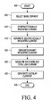
- FIG. 4 a flow diagram depicting the method of adding current of the least significant bits of a digital to analog converter according to one embodiment of the invention is shown.
- the process begins with Start 400 .
- a base current, IO is selected in step 405 .
- a 1 uA current is selected.
- the total current and voltage to be supplied by the multipurpose digital to analog converter 116 is determined.
- the number of MSBs 208 and LSBs 210 are selected as well as the current levels for each. Again, a wide variety of MSB and LSB combinations, as well as total current levels, may be selected without detracting from the spirit of the invention.
- an equally weighted current is generated through the MSB transistors 216 .
- the IO is set to 1 uA and the current generated through a MSB transistor 216 is 128 times the base current (IO).
- the current for the upper LSBs 210 is generated.
- the current for the upper LSBs 232 is generated through each first LSB transistors 217 and is eight (8) times the base current (IO).
- the current for the lower LSBs 234 is generated through the second, third, and fourth transistors 218 , 220 , and 222 , and is four (4), two (2), and one (1) times the base current (IO) accordingly.
- An IO current is generated through the LSB ground transistor 223 and passed directly to ground.
- the total LSB current both for upper LSB 232 and lower LSB 234 , is provided through the LSB master transistor 1216 .
- the maximum current for the LSBs 210 without any additional current from the overlap adjustment circuitry 212 is equal to or less than the current for a single MSB 208 .
- the actual MSB current for each MSB and the total LSB current is determined in step 425 . All LSBs 210 are placed “ON” and the total actual current provided by all of the LSBs is determined. The actual current is then compared to the ideal current and the current level for each MSB 208 .
- An overlap current level is determined and generated in step 430 . Once all of the MSB 208 currents and the total LSB 210 current has been measured, the largest MSB 208 current is determined. The total LSB 210 current plus the overlap current must exceed the largest MSB 208 current to ensure no missing steps. Based upon this information, the overlap current level is calculated. Once the additional current level is determined, the overlap adjustment circuitry is programmed to provide the additional current. No additional programming of the overlap adjustment circuit 212 is necessary after the initial programming. In another embodiment, the total actual current provided by the LSBs 210 and the overlap adjustment circuitry 212 is repeatedly measured and programmed until the additional current, combined with the actual LSB 210 current, exceeds the actual and ideal current for the MSB 208 . The method ends with step 435 .
- a digital to analog converter including a current source for providing a master current, a first sub digital to analog converter coupled to the current source, wherein the first sub digital to analog converter generates a plurality of currents, a second sub digital to analog converter coupled to at least one of the plurality of currents from the first sub digital to analog converter, wherein the second sub digital to analog converter generates a second plurality of currents, and an overlap adjustment circuit coupled with the second sub digital to analog converter, wherein the overlap adjustment circuit adds current and wherein the digital to analog converter is configured to operate in a first mode for generating a sine wave wherein the sine wave has a first bit level accuracy and wherein the overlap adjustment circuit adds no current to the second sub digital to analog converter and wherein the digital to analog converter is configured to operate in a second mode for generating a ramp wave wherein the ramp wave has a second bit level accuracy and wherein the overlap adjustment circuit adds current to the second sub digital to analog converter, and wherein, during the second mode, the total current of the second
- the currents of the first sub-digital to analog converter include the most significant bits and the currents of the second sub-digital to analog converter include the least significant bits. Further, the currents from the first sub-digital to analog converter include a plurality of currents each equal to the master current and the currents from the second sub-digital to analog converter include a second plurality of currents cumulatively equal to a single current generated by the first sub digital to analog converter.
- the most significant bits include five most significant bits and the least significant bits include seven least significant bits and the currents of the least significant bits are variably weighted, including binary weighted currents.
- the current of one most significant bit is greater than or equal to the current of all of the least significant bits and the sine wave first bit level accuracy is a ten bit level accuracy and the ramp wave second bit level accuracy is a twelve bit level accuracy.
- a frequency modulated continuous wave transceiver with a multiple mode digital to analog converter including an analog to digital converter, a digital to analog converter coupled to a voltage controlled oscillator, the digital to analog converter further including a current source for providing a master current, a first sub digital to analog converter coupled to the current source, wherein the first sub digital to analog converter generates a plurality of currents, a second sub digital to analog converter coupled to at least one of the plurality of currents from the first sub digital to analog converter, wherein the second sub digital to analog converter generates a second plurality of currents and an overlap adjustment circuit coupled with the second sub digital to analog converter, wherein the overlap adjustment circuit adds current, wherein the digital to analog converter is configured to operate in a first mode for generating a sine wave to the analog to digital converter wherein the sine wave has a first bit level accuracy and wherein the overlap adjustment circuit adds no current and wherein the digital to analog converter is configured to operate in a second mode for generating a ramp wave to the voltage controlled oscill
- the digital to analog converter generates a falling ramp signal, including a 12 bit level accuracy falling ramp signal.
- the digital to analog converter also generates a sine wave for transmission to the analog to digital converter, including continuous time sigma delta analog to digital converters, the generated sine wave for use as an element of an internal check.
- the generated sine wave includes a ten bit level accuracy sine wave.
- a method of transitioning from all of the least significant bits to a most significant bit in a digital to analog converter including the steps of: generating a current for each most significant bit, generating a second current to each of a first set of the least significant bits and generating a third current to a second set of the least significant bits, wherein the sum of the second and third currents equals the current for a most significant bit, and generating an overlap current to add to the total current of the least significant bits, wherein the total current of the least significant bits with the overlap current is greater than the current from a single most significant bit.
- the current for each most significant bit is equal and each second current for the first set of least significant bits is equal and the third current of the second set of the least significant bits is binary weighted. Further, the method including measuring the current from the most significant bits and the least significant bits, wherein the overlap current is programmed in relation to the measured current from the most significant bits and the least significant bits.
- the various diagrams may depict an example architectural or other configuration for the invention, which is done to aid in understanding the features and functionality that can be included in the invention.
- the invention is not restricted to the illustrated example architectures or configurations, but the desired features can be implemented using a variety of alternative architectures and configurations. Indeed, it will be apparent to one of skill in the art how alternative functional, logical or physical partitioning and configurations can be implemented to implement the desired features of the invention. Also, a multitude of different constituent module names other than those depicted herein can be applied to the various partitions. Additionally, with regard to flow diagrams, operational descriptions and method claims, the order in which the steps are presented herein shall not mandate that various embodiments be implemented to perform the recited functionality in the same order unless the context dictates otherwise.
- a group of items linked with the conjunction “and” should not be read as requiring that each and every one of those items be present in the grouping, but rather should be read as “and/or” unless expressly stated otherwise.
- a group of items linked with the conjunction “or” should not be read as requiring mutual exclusivity among that group, but rather should also be read as “and/or” unless expressly stated otherwise.
- items, elements or components of the invention may be described or claimed in the singular, the plural is contemplated to be within the scope thereof unless limitation to the singular is explicitly stated.
- module does not imply that the components or functionality described or claimed as part of the module are all configured in a common package. Indeed, any or all of the various components of a module, whether control logic or other components, can be combined in a single package or separately maintained and can further be distributed across multiple locations.
Abstract
Description
| TABLE 1 |
| Digital Input Code (Decimal Format) |
| 0 | • • • | 126 | 127 | 128 | • • • | 254 | 255 | 256 | ||
| Analog | no_overlap | 0 | • • • | 126 | 127 | 128 | • • • | 254 | 255 | 256 |
| Current | 2 bit overlap | 0 | • • • | 128.9764 | 130 | 128 | • • • | 256.9764 | 258 | 256 |
| |
3 bit overlap | 0 | • • • | 132.9449 | 134 | 128 | • • • | 260.9449 | 262 | 256 |
| (uA) | 4 bit overlap | 0 | • • • | 140.8819 | 142 | 128 | • • • | 268.8819 | 270 | 256 |
| TABLE 2 |
| LSB Calculation |
| Overlap | Total | Second Sub-Digital to | ||
| Overlap | Adjustment | LSB | Analog Converter | |
| Adjustment | current | current | (LSB) size | |
| code | (uA) | (uA) | (uA) | |
| no_overlap | 0000 | 0 | 127 | 1 |
| 2 bit overlap | 0011 | 3 | 130 | 1.023622047 |
| 3 bit overlap | 0111 | 7 | 134 | 1.05511811 |
| 4 bit overlap | 1111 | 15 | 142 | 1.118110236 |
Claims (15)
Priority Applications (2)
| Application Number | Priority Date | Filing Date | Title |
|---|---|---|---|
| US14/644,941 US9264062B1 (en) | 2015-03-11 | 2015-03-11 | Digital-to-analog converter circuit |
| US14/991,869 US9548757B2 (en) | 2015-03-11 | 2016-01-08 | Digital-to-analog converter circuit |
Applications Claiming Priority (1)
| Application Number | Priority Date | Filing Date | Title |
|---|---|---|---|
| US14/644,941 US9264062B1 (en) | 2015-03-11 | 2015-03-11 | Digital-to-analog converter circuit |
Related Child Applications (1)
| Application Number | Title | Priority Date | Filing Date |
|---|---|---|---|
| US14/991,869 Continuation US9548757B2 (en) | 2015-03-11 | 2016-01-08 | Digital-to-analog converter circuit |
Publications (1)
| Publication Number | Publication Date |
|---|---|
| US9264062B1 true US9264062B1 (en) | 2016-02-16 |
Family
ID=55275533
Family Applications (2)
| Application Number | Title | Priority Date | Filing Date |
|---|---|---|---|
| US14/644,941 Active US9264062B1 (en) | 2015-03-11 | 2015-03-11 | Digital-to-analog converter circuit |
| US14/991,869 Active US9548757B2 (en) | 2015-03-11 | 2016-01-08 | Digital-to-analog converter circuit |
Family Applications After (1)
| Application Number | Title | Priority Date | Filing Date |
|---|---|---|---|
| US14/991,869 Active US9548757B2 (en) | 2015-03-11 | 2016-01-08 | Digital-to-analog converter circuit |
Country Status (1)
| Country | Link |
|---|---|
| US (2) | US9264062B1 (en) |
Cited By (4)
| Publication number | Priority date | Publication date | Assignee | Title |
|---|---|---|---|---|
| US9548757B2 (en) * | 2015-03-11 | 2017-01-17 | Nxp Usa, Inc. | Digital-to-analog converter circuit |
| CN109428599A (en) * | 2017-08-31 | 2019-03-05 | 亚德诺半导体无限责任公司 | With improved linear digital analog converter |
| US10615817B2 (en) * | 2017-11-07 | 2020-04-07 | Analog Devices Global Unlimited Company | Current steering digital to analog converter |
| US20220278691A1 (en) * | 2021-02-26 | 2022-09-01 | Seiko Epson Corporation | A/D Converter, Digital-Output Temperature Sensor, Circuit Device, And Oscillator |
Families Citing this family (1)
| Publication number | Priority date | Publication date | Assignee | Title |
|---|---|---|---|---|
| EP3667923A1 (en) * | 2018-12-11 | 2020-06-17 | IMEC vzw | Frequency dac for radar |
Citations (14)
| Publication number | Priority date | Publication date | Assignee | Title |
|---|---|---|---|---|
| US5870044A (en) * | 1996-11-14 | 1999-02-09 | Sgs-Thomson Microelectronics S.A. | Digital analog converter with self-calibration current sources |
| US6072415A (en) * | 1998-10-29 | 2000-06-06 | Neomagic Corp. | Multi-mode 8/9-bit DAC with variable input-precision and output range for VGA and NTSC outputs |
| US20020008651A1 (en) * | 2000-07-20 | 2002-01-24 | Alexander Bugeja | Segmented high speed and high resolution digital-to-analog converter |
| US20020167430A1 (en) * | 2001-05-09 | 2002-11-14 | Broadcom Corporation | Digital-to-analogue converter using an array of current sources |
| US20030001765A1 (en) * | 2001-06-22 | 2003-01-02 | Bright William J. | Correction circuit for beta mismatch between thermometer encoded and R-2R ladder segments of a current steering DAC |
| US6650265B1 (en) * | 2001-04-30 | 2003-11-18 | Engim, Inc. | Method and architecture for varying power consumption of a current mode digital/analog converter in proportion to performance parameters |
| US6674377B1 (en) * | 2002-04-25 | 2004-01-06 | Rambus Inc. | Circuit, apparatus and method for improved current distribution of output drivers enabling improved calibration efficiency and accuracy |
| US20040233089A1 (en) * | 2003-03-14 | 2004-11-25 | Stmicroelectronics S.R.L. | High resolution and low consumption digital-analog converter |
| US7173553B2 (en) * | 2004-09-29 | 2007-02-06 | Matsushita Electric Industrial Co., Ltd. | Current summing digital-to-analog converter |
| US7466252B1 (en) * | 2007-07-12 | 2008-12-16 | Xilinx, Inc. | Method and apparatus for calibrating a scaled current electronic circuit |
| US20100164766A1 (en) * | 2008-12-31 | 2010-07-01 | Fang-Shi Jordan Lai | DAC Variation-Tracking Calibration |
| US20100289680A1 (en) * | 2009-05-15 | 2010-11-18 | Realtek Semiconductor Corp. | Self-Calibrated Current Source and DAC Using the Same and Operation Method Thereof |
| US8094055B2 (en) * | 2010-01-26 | 2012-01-10 | Power Integrations, Inc. | Compact digital-to-analog converter |
| US8284099B2 (en) | 2010-03-19 | 2012-10-09 | Kabushiki Kaisha Toshiba | FMCW signal generation circuit and radar apparatus |
Family Cites Families (11)
| Publication number | Priority date | Publication date | Assignee | Title |
|---|---|---|---|---|
| US6326909B1 (en) * | 1997-09-18 | 2001-12-04 | Advantest Corporation | Evaluation system for analog-digital or digital-analog converter |
| DE19813604A1 (en) * | 1998-03-27 | 1999-09-30 | Daimler Benz Aerospace Ag | Arrangement for precise distance measurement, especially for level measurement |
| US6621439B1 (en) * | 2001-04-30 | 2003-09-16 | Engim, Inc. | Method for implementing a segmented current-mode digital/analog converter with matched segment time constants |
| EP1465347B9 (en) * | 2003-03-31 | 2007-11-14 | AMI Semiconductor Belgium BVBA | Monotonic precise current DAC |
| US7019677B1 (en) * | 2004-09-08 | 2006-03-28 | Cirrus Logic, Inc. | Current steering digital to analog converters with self-calibration, and systems and methods using the same |
| TWI244270B (en) * | 2005-01-17 | 2005-11-21 | Novatek Microelectronics Corp | Digital-to-analog converter |
| US7646235B2 (en) * | 2007-02-13 | 2010-01-12 | Infineon Technologies Ag | Programmable current generator, current generation method and transmitter arrangement |
| CN102124654B (en) * | 2008-08-19 | 2013-10-30 | 松下电器产业株式会社 | Oversampling A/D converter |
| US8253809B2 (en) * | 2008-08-27 | 2012-08-28 | Sony Corporation | Analog-digital converter, analog-digital conversion method, image pickup device, method of driving the same, and camera |
| US7986255B2 (en) * | 2009-11-24 | 2011-07-26 | Nxp B.V. | High resolution overlapping bit segmented DAC |
| US9264062B1 (en) * | 2015-03-11 | 2016-02-16 | Freescale Semiconductor, Inc. | Digital-to-analog converter circuit |
-
2015
- 2015-03-11 US US14/644,941 patent/US9264062B1/en active Active
-
2016
- 2016-01-08 US US14/991,869 patent/US9548757B2/en active Active
Patent Citations (14)
| Publication number | Priority date | Publication date | Assignee | Title |
|---|---|---|---|---|
| US5870044A (en) * | 1996-11-14 | 1999-02-09 | Sgs-Thomson Microelectronics S.A. | Digital analog converter with self-calibration current sources |
| US6072415A (en) * | 1998-10-29 | 2000-06-06 | Neomagic Corp. | Multi-mode 8/9-bit DAC with variable input-precision and output range for VGA and NTSC outputs |
| US20020008651A1 (en) * | 2000-07-20 | 2002-01-24 | Alexander Bugeja | Segmented high speed and high resolution digital-to-analog converter |
| US6650265B1 (en) * | 2001-04-30 | 2003-11-18 | Engim, Inc. | Method and architecture for varying power consumption of a current mode digital/analog converter in proportion to performance parameters |
| US20020167430A1 (en) * | 2001-05-09 | 2002-11-14 | Broadcom Corporation | Digital-to-analogue converter using an array of current sources |
| US20030001765A1 (en) * | 2001-06-22 | 2003-01-02 | Bright William J. | Correction circuit for beta mismatch between thermometer encoded and R-2R ladder segments of a current steering DAC |
| US6674377B1 (en) * | 2002-04-25 | 2004-01-06 | Rambus Inc. | Circuit, apparatus and method for improved current distribution of output drivers enabling improved calibration efficiency and accuracy |
| US20040233089A1 (en) * | 2003-03-14 | 2004-11-25 | Stmicroelectronics S.R.L. | High resolution and low consumption digital-analog converter |
| US7173553B2 (en) * | 2004-09-29 | 2007-02-06 | Matsushita Electric Industrial Co., Ltd. | Current summing digital-to-analog converter |
| US7466252B1 (en) * | 2007-07-12 | 2008-12-16 | Xilinx, Inc. | Method and apparatus for calibrating a scaled current electronic circuit |
| US20100164766A1 (en) * | 2008-12-31 | 2010-07-01 | Fang-Shi Jordan Lai | DAC Variation-Tracking Calibration |
| US20100289680A1 (en) * | 2009-05-15 | 2010-11-18 | Realtek Semiconductor Corp. | Self-Calibrated Current Source and DAC Using the Same and Operation Method Thereof |
| US8094055B2 (en) * | 2010-01-26 | 2012-01-10 | Power Integrations, Inc. | Compact digital-to-analog converter |
| US8284099B2 (en) | 2010-03-19 | 2012-10-09 | Kabushiki Kaisha Toshiba | FMCW signal generation circuit and radar apparatus |
Non-Patent Citations (4)
| Title |
|---|
| Lin et al., "A 10-b, 500-MSample/s CMOS DAC in 0.6 mm2", IEEE Journal of Solid-State Circuits, vol. 33, No. 12, Dec. 1998, pp. 1948-1958. |
| Mitomo et al., "A 77 GHz 90 nm CMOS Transceiver for FMCW Radar Applications", IEEE Journal of Solid-State Circuits, vol. 45, No. 4, Apr. 2010, pp. 928-937. |
| Sakurai et al., "A 1.5GHz-Modulation-Range 10ms-Modulation-Period 180kHzms Frequency-Error 26MHz-Reference Mixed-Mode FMCW Synthesizer for mm-Wave Radar Application", ISSCC 2011, Session 16, mm-Wave Design Techniques, 16.8, pp. 292-294. |
| Wu et al., "A 56.4-to-63.4 GHz Multi-Rate All-Digital Fractional-N PLL for FMCW Radar Applications in 65 nm CMOS", IEEE Journal of Solid-State Circuits, vol. 49, No. 5, May 2014, pp. 1081-1096. |
Cited By (6)
| Publication number | Priority date | Publication date | Assignee | Title |
|---|---|---|---|---|
| US9548757B2 (en) * | 2015-03-11 | 2017-01-17 | Nxp Usa, Inc. | Digital-to-analog converter circuit |
| CN109428599A (en) * | 2017-08-31 | 2019-03-05 | 亚德诺半导体无限责任公司 | With improved linear digital analog converter |
| CN109428599B (en) * | 2017-08-31 | 2022-05-31 | 亚德诺半导体国际无限责任公司 | Digital-to-analog converter with improved linearity |
| US10615817B2 (en) * | 2017-11-07 | 2020-04-07 | Analog Devices Global Unlimited Company | Current steering digital to analog converter |
| US20220278691A1 (en) * | 2021-02-26 | 2022-09-01 | Seiko Epson Corporation | A/D Converter, Digital-Output Temperature Sensor, Circuit Device, And Oscillator |
| US11916560B2 (en) * | 2021-02-26 | 2024-02-27 | Seiko Epson Corporation | A/D converter, digital-output temperature sensor, circuit device, and oscillator |
Also Published As
| Publication number | Publication date |
|---|---|
| US20160269041A1 (en) | 2016-09-15 |
| US9548757B2 (en) | 2017-01-17 |
Similar Documents
| Publication | Publication Date | Title |
|---|---|---|
| US9548757B2 (en) | Digital-to-analog converter circuit | |
| CN100481730C (en) | Method for calibrating digital-to-analog converter and digital-to-analog converter | |
| US6914547B1 (en) | Triple resistor string DAC architecture | |
| US9136866B2 (en) | Digital-to-analog converter and a method of operating a digital-to-analog converter | |
| US10305505B1 (en) | Interpolation digital-to-analog converter (DAC) | |
| JPH0964746A (en) | D/a converter | |
| US20130293405A1 (en) | Segmented digital-to-analog converter having weighted current sources | |
| US8581766B1 (en) | DAC with novel switch regulation | |
| US7564385B2 (en) | Current compensation for digital-to-analog converter | |
| JP4671766B2 (en) | Digital-analog converter and digital-analog conversion method | |
| CN114650061A (en) | Integrated circuit, digital-to-analog converter and driving method thereof | |
| CN110912561B (en) | Digital-to-analog converter transfer function modification | |
| US11303294B2 (en) | Digital to analog converters | |
| US6642867B1 (en) | Replica compensated heterogeneous DACs and methods | |
| US8390498B2 (en) | Comparing circuit and parallel analog-to-digital converter | |
| US8717214B1 (en) | Precision sub-RADIX2 DAC with linearity calibration | |
| US10630303B1 (en) | Digital-to-analog conversion device and compensation circuit | |
| Baranwal et al. | Design and analysis of 8 bit fully segmented digital to analog converter | |
| US6856174B1 (en) | Versatile system for high resolution device calibration | |
| CN117375613B (en) | Calibration circuit and method for current source array in multichannel current steering DAC | |
| Huq et al. | Design of low power 8-bit DAC using PTM-LP technology | |
| US7375671B1 (en) | Systems and methods for reducing transient errors on digital to analog converters (DACs) deglitcher | |
| Kazmi | Low Power CMOS 8-Bit Current Steering DAC | |
| Hatamzadeh et al. | A New 12-bit 100-MS/Sec Resistor String DAC in 0.35-μm CMOS Process | |
| Chen et al. | Nonlinearity analysis of folded Multi-LSB decided resistor string digital to analog converter |
Legal Events
| Date | Code | Title | Description |
|---|---|---|---|
| AS | Assignment |
Owner name: FREESCALE SEMICONDUCTOR, INC., TEXAS Free format text: ASSIGNMENT OF ASSIGNORS INTEREST;ASSIGNORS:KABIR, MOHAMMAD NIZAM;BRASWELL, BRANDT;HOSEINI, MARIAM;REEL/FRAME:035142/0255 Effective date: 20150310 |
|
| AS | Assignment |
Owner name: CITIBANK, N.A., AS NOTES COLLATERAL AGENT, NEW YORK Free format text: SUPPLEMENT TO IP SECURITY AGREEMENT;ASSIGNOR:FREESCALE SEMICONDUCTOR, INC.;REEL/FRAME:035571/0112 Effective date: 20150428 Owner name: CITIBANK, N.A., AS NOTES COLLATERAL AGENT, NEW YORK Free format text: SUPPLEMENT TO IP SECURITY AGREEMENT;ASSIGNOR:FREESCALE SEMICONDUCTOR, INC.;REEL/FRAME:035571/0095 Effective date: 20150428 Owner name: CITIBANK, N.A., AS NOTES COLLATERAL AGENT, NEW YORK Free format text: SUPPLEMENT TO IP SECURITY AGREEMENT;ASSIGNOR:FREESCALE SEMICONDUCTOR, INC.;REEL/FRAME:035571/0080 Effective date: 20150428 Owner name: CITIBANK, N.A., AS NOTES COLLATERAL AGENT, NEW YOR Free format text: SUPPLEMENT TO IP SECURITY AGREEMENT;ASSIGNOR:FREESCALE SEMICONDUCTOR, INC.;REEL/FRAME:035571/0095 Effective date: 20150428 Owner name: CITIBANK, N.A., AS NOTES COLLATERAL AGENT, NEW YOR Free format text: SUPPLEMENT TO IP SECURITY AGREEMENT;ASSIGNOR:FREESCALE SEMICONDUCTOR, INC.;REEL/FRAME:035571/0112 Effective date: 20150428 Owner name: CITIBANK, N.A., AS NOTES COLLATERAL AGENT, NEW YOR Free format text: SUPPLEMENT TO IP SECURITY AGREEMENT;ASSIGNOR:FREESCALE SEMICONDUCTOR, INC.;REEL/FRAME:035571/0080 Effective date: 20150428 |
|
| AS | Assignment |
Owner name: FREESCALE SEMICONDUCTOR, INC., TEXAS Free format text: PATENT RELEASE;ASSIGNOR:CITIBANK, N.A., AS COLLATERAL AGENT;REEL/FRAME:037357/0974 Effective date: 20151207 |
|
| AS | Assignment |
Owner name: MORGAN STANLEY SENIOR FUNDING, INC., MARYLAND Free format text: ASSIGNMENT AND ASSUMPTION OF SECURITY INTEREST IN PATENTS;ASSIGNOR:CITIBANK, N.A.;REEL/FRAME:037458/0359 Effective date: 20151207 Owner name: MORGAN STANLEY SENIOR FUNDING, INC., MARYLAND Free format text: ASSIGNMENT AND ASSUMPTION OF SECURITY INTEREST IN PATENTS;ASSIGNOR:CITIBANK, N.A.;REEL/FRAME:037458/0341 Effective date: 20151207 |
|
| STCF | Information on status: patent grant |
Free format text: PATENTED CASE |
|
| AS | Assignment |
Owner name: MORGAN STANLEY SENIOR FUNDING, INC., MARYLAND Free format text: SUPPLEMENT TO THE SECURITY AGREEMENT;ASSIGNOR:FREESCALE SEMICONDUCTOR, INC.;REEL/FRAME:039138/0001 Effective date: 20160525 |
|
| AS | Assignment |
Owner name: NXP, B.V., F/K/A FREESCALE SEMICONDUCTOR, INC., NETHERLANDS Free format text: RELEASE BY SECURED PARTY;ASSIGNOR:MORGAN STANLEY SENIOR FUNDING, INC.;REEL/FRAME:040925/0001 Effective date: 20160912 Owner name: NXP, B.V., F/K/A FREESCALE SEMICONDUCTOR, INC., NE Free format text: RELEASE BY SECURED PARTY;ASSIGNOR:MORGAN STANLEY SENIOR FUNDING, INC.;REEL/FRAME:040925/0001 Effective date: 20160912 |
|
| AS | Assignment |
Owner name: NXP B.V., NETHERLANDS Free format text: RELEASE BY SECURED PARTY;ASSIGNOR:MORGAN STANLEY SENIOR FUNDING, INC.;REEL/FRAME:040928/0001 Effective date: 20160622 |
|
| AS | Assignment |
Owner name: NXP USA, INC., TEXAS Free format text: MERGER;ASSIGNOR:FREESCALE SEMICONDUCTOR, INC.;REEL/FRAME:041144/0363 Effective date: 20161107 |
|
| MAFP | Maintenance fee payment |
Free format text: PAYMENT OF MAINTENANCE FEE, 4TH YEAR, LARGE ENTITY (ORIGINAL EVENT CODE: M1551); ENTITY STATUS OF PATENT OWNER: LARGE ENTITY Year of fee payment: 4 |
|
| AS | Assignment |
Owner name: NXP B.V., NETHERLANDS Free format text: RELEASE BY SECURED PARTY;ASSIGNOR:MORGAN STANLEY SENIOR FUNDING, INC.;REEL/FRAME:050744/0097 Effective date: 20190903 |
|
| AS | Assignment |
Owner name: NXP B.V., NETHERLANDS Free format text: CORRECTIVE ASSIGNMENT TO CORRECT THE REMOVEAPPLICATION 11759915 AND REPLACE IT WITH APPLICATION11759935 PREVIOUSLY RECORDED ON REEL 040928 FRAME 0001. ASSIGNOR(S) HEREBY CONFIRMS THE RELEASE OF SECURITYINTEREST;ASSIGNOR:MORGAN STANLEY SENIOR FUNDING, INC.;REEL/FRAME:052915/0001 Effective date: 20160622 |
|
| AS | Assignment |
Owner name: NXP, B.V. F/K/A FREESCALE SEMICONDUCTOR, INC., NETHERLANDS Free format text: CORRECTIVE ASSIGNMENT TO CORRECT THE REMOVEAPPLICATION 11759915 AND REPLACE IT WITH APPLICATION11759935 PREVIOUSLY RECORDED ON REEL 040925 FRAME 0001. ASSIGNOR(S) HEREBY CONFIRMS THE RELEASE OF SECURITYINTEREST;ASSIGNOR:MORGAN STANLEY SENIOR FUNDING, INC.;REEL/FRAME:052917/0001 Effective date: 20160912 |
|
| MAFP | Maintenance fee payment |
Free format text: PAYMENT OF MAINTENANCE FEE, 8TH YEAR, LARGE ENTITY (ORIGINAL EVENT CODE: M1552); ENTITY STATUS OF PATENT OWNER: LARGE ENTITY Year of fee payment: 8 |