US9270390B2 - Frequency and phase offset compensation of modulated signals with symbol timing recovery - Google Patents
Frequency and phase offset compensation of modulated signals with symbol timing recovery Download PDFInfo
- Publication number
- US9270390B2 US9270390B2 US14/229,761 US201414229761A US9270390B2 US 9270390 B2 US9270390 B2 US 9270390B2 US 201414229761 A US201414229761 A US 201414229761A US 9270390 B2 US9270390 B2 US 9270390B2
- Authority
- US
- United States
- Prior art keywords
- signal
- digital information
- information signal
- transformation
- frequency
- Prior art date
- Legal status (The legal status is an assumption and is not a legal conclusion. Google has not performed a legal analysis and makes no representation as to the accuracy of the status listed.)
- Expired - Fee Related
Links
- 238000011084 recovery Methods 0.000 title abstract description 17
- 230000009466 transformation Effects 0.000 claims abstract description 59
- 238000000034 method Methods 0.000 claims abstract description 36
- 230000003111 delayed effect Effects 0.000 claims description 16
- 238000012937 correction Methods 0.000 claims description 6
- 238000005070 sampling Methods 0.000 claims description 5
- 238000001228 spectrum Methods 0.000 claims description 4
- 238000000844 transformation Methods 0.000 claims 6
- 238000005516 engineering process Methods 0.000 description 63
- 238000004891 communication Methods 0.000 description 44
- 238000010586 diagram Methods 0.000 description 40
- 238000012545 processing Methods 0.000 description 14
- 230000006870 function Effects 0.000 description 9
- 239000000203 mixture Substances 0.000 description 7
- 230000008569 process Effects 0.000 description 7
- 238000004590 computer program Methods 0.000 description 6
- 230000001934 delay Effects 0.000 description 6
- 238000013459 approach Methods 0.000 description 5
- 230000007246 mechanism Effects 0.000 description 5
- 230000003287 optical effect Effects 0.000 description 5
- 238000001914 filtration Methods 0.000 description 4
- 230000010363 phase shift Effects 0.000 description 4
- 230000005540 biological transmission Effects 0.000 description 2
- 230000001413 cellular effect Effects 0.000 description 2
- 238000006243 chemical reaction Methods 0.000 description 2
- 230000001427 coherent effect Effects 0.000 description 2
- 239000000284 extract Substances 0.000 description 2
- 230000004044 response Effects 0.000 description 2
- 230000003068 static effect Effects 0.000 description 2
- 230000003044 adaptive effect Effects 0.000 description 1
- 239000000654 additive Substances 0.000 description 1
- 230000000996 additive effect Effects 0.000 description 1
- 230000004075 alteration Effects 0.000 description 1
- 230000003321 amplification Effects 0.000 description 1
- 238000003491 array Methods 0.000 description 1
- 230000000295 complement effect Effects 0.000 description 1
- 230000006835 compression Effects 0.000 description 1
- 238000007906 compression Methods 0.000 description 1
- 239000000470 constituent Substances 0.000 description 1
- 238000001514 detection method Methods 0.000 description 1
- 235000019800 disodium phosphate Nutrition 0.000 description 1
- 230000000694 effects Effects 0.000 description 1
- 238000000605 extraction Methods 0.000 description 1
- 230000003993 interaction Effects 0.000 description 1
- 238000012423 maintenance Methods 0.000 description 1
- 230000004048 modification Effects 0.000 description 1
- 238000012986 modification Methods 0.000 description 1
- 238000003199 nucleic acid amplification method Methods 0.000 description 1
- 238000005192 partition Methods 0.000 description 1
- 230000002093 peripheral effect Effects 0.000 description 1
- 229920000747 poly(lactic acid) Polymers 0.000 description 1
- 238000007639 printing Methods 0.000 description 1
- 230000035755 proliferation Effects 0.000 description 1
- 238000000638 solvent extraction Methods 0.000 description 1
Images


Classifications
-
- H—ELECTRICITY
- H04—ELECTRIC COMMUNICATION TECHNIQUE
- H04L—TRANSMISSION OF DIGITAL INFORMATION, e.g. TELEGRAPHIC COMMUNICATION
- H04L7/00—Arrangements for synchronising receiver with transmitter
- H04L7/0054—Detection of the synchronisation error by features other than the received signal transition
- H04L7/007—Detection of the synchronisation error by features other than the received signal transition detection of error based on maximum signal power, e.g. peak value, maximizing autocorrelation
-
- H—ELECTRICITY
- H04—ELECTRIC COMMUNICATION TECHNIQUE
- H04B—TRANSMISSION
- H04B17/00—Monitoring; Testing
- H04B17/20—Monitoring; Testing of receivers
-
- H—ELECTRICITY
- H04—ELECTRIC COMMUNICATION TECHNIQUE
- H04L—TRANSMISSION OF DIGITAL INFORMATION, e.g. TELEGRAPHIC COMMUNICATION
- H04L27/00—Modulated-carrier systems
- H04L27/0014—Carrier regulation
-
- H—ELECTRICITY
- H04—ELECTRIC COMMUNICATION TECHNIQUE
- H04L—TRANSMISSION OF DIGITAL INFORMATION, e.g. TELEGRAPHIC COMMUNICATION
- H04L27/00—Modulated-carrier systems
- H04L27/10—Frequency-modulated carrier systems, i.e. using frequency-shift keying
- H04L27/14—Demodulator circuits; Receiver circuits
-
- H—ELECTRICITY
- H04—ELECTRIC COMMUNICATION TECHNIQUE
- H04L—TRANSMISSION OF DIGITAL INFORMATION, e.g. TELEGRAPHIC COMMUNICATION
- H04L27/00—Modulated-carrier systems
- H04L27/18—Phase-modulated carrier systems, i.e. using phase-shift keying
- H04L27/22—Demodulator circuits; Receiver circuits
-
- H—ELECTRICITY
- H04—ELECTRIC COMMUNICATION TECHNIQUE
- H04L—TRANSMISSION OF DIGITAL INFORMATION, e.g. TELEGRAPHIC COMMUNICATION
- H04L27/00—Modulated-carrier systems
- H04L27/18—Phase-modulated carrier systems, i.e. using phase-shift keying
- H04L27/22—Demodulator circuits; Receiver circuits
- H04L27/227—Demodulator circuits; Receiver circuits using coherent demodulation
- H04L27/2271—Demodulator circuits; Receiver circuits using coherent demodulation wherein the carrier recovery circuit uses only the demodulated signals
-
- H—ELECTRICITY
- H04—ELECTRIC COMMUNICATION TECHNIQUE
- H04L—TRANSMISSION OF DIGITAL INFORMATION, e.g. TELEGRAPHIC COMMUNICATION
- H04L27/00—Modulated-carrier systems
- H04L27/32—Carrier systems characterised by combinations of two or more of the types covered by groups H04L27/02, H04L27/10, H04L27/18 or H04L27/26
- H04L27/34—Amplitude- and phase-modulated carrier systems, e.g. quadrature-amplitude modulated carrier systems
- H04L27/38—Demodulator circuits; Receiver circuits
- H04L27/3818—Demodulator circuits; Receiver circuits using coherent demodulation, i.e. using one or more nominally phase synchronous carriers
- H04L27/3827—Demodulator circuits; Receiver circuits using coherent demodulation, i.e. using one or more nominally phase synchronous carriers in which the carrier is recovered using only the demodulated baseband signals
-
- H—ELECTRICITY
- H04—ELECTRIC COMMUNICATION TECHNIQUE
- H04L—TRANSMISSION OF DIGITAL INFORMATION, e.g. TELEGRAPHIC COMMUNICATION
- H04L7/00—Arrangements for synchronising receiver with transmitter
- H04L7/0054—Detection of the synchronisation error by features other than the received signal transition
-
- H—ELECTRICITY
- H04—ELECTRIC COMMUNICATION TECHNIQUE
- H04B—TRANSMISSION
- H04B1/00—Details of transmission systems, not covered by a single one of groups H04B3/00 - H04B13/00; Details of transmission systems not characterised by the medium used for transmission
- H04B1/06—Receivers
- H04B1/10—Means associated with receiver for limiting or suppressing noise or interference
- H04B1/1027—Means associated with receiver for limiting or suppressing noise or interference assessing signal quality or detecting noise/interference for the received signal
-
- H—ELECTRICITY
- H04—ELECTRIC COMMUNICATION TECHNIQUE
- H04L—TRANSMISSION OF DIGITAL INFORMATION, e.g. TELEGRAPHIC COMMUNICATION
- H04L27/00—Modulated-carrier systems
- H04L27/0014—Carrier regulation
- H04L2027/0024—Carrier regulation at the receiver end
- H04L2027/0026—Correction of carrier offset
- H04L2027/0036—Correction of carrier offset using a recovered symbol clock
Definitions
- the disclosed technology relates generally to communication systems, and more particularly, some embodiments relate to systems and methods for frequency and phase offset compensation with symbol timing recovery for received modulated signals.
- Wireless communication devices have become ubiquitous in today's society. Indeed, with the many continued advancements in communication technology, more and more devices are being introduced in both the consumer, commercial, and government sectors with advanced communications capabilities. Additionally, advances in processing power and low-power consumption technologies, as well as advances in data coding and modulation techniques have led to the proliferation of wired and wireless communications capabilities on a more widespread basis.
- communication networks both wired and wireless
- networks allow various heretofore independent devices to share data and other information to enhance productivity or simply to improve their convenience to the user.
- exemplary networks include the Bluetooth® communications network and various IEEE standards-based networks such as 802.11 and 802.16 communications networks, to name a few.
- wireless communication capabilities can allow for information exchange including information such as, for example, command and control information to control the equipment; telemetry, data, or other information gathered by the equipment; status, reports, and other like “housekeeping” information; as well as other information that may be useful or necessary in the operation, use, deployment and maintenance of the equipment.
- FIG. 1 is a simplified block diagram illustrating an example of a transmitter and a receiver that can be used with any of a number of wireless devices including equipment of the type mentioned above. Depending on the desired capabilities, these devices can include a transmitter, a receiver, or both (referred to as a transceiver).
- the transmitter receives information 122 for transmission, and may include a precoder 132 , a modulator 134 , an amplifier 136 , and an antenna 138 .
- Precoder 132 can be included to, for example, precode the data to optimize performance by taking into account channel parameters or characteristics.
- Modulator 134 is essentially used to receive the information to be transmitted and output a radio frequency (RF) modulated signal. Modulation is typically achieved by combining (e.g. multiplying) the information signal 122 (whether or not precoded) with a carrier wave at the desired carrier frequency. Modulation can be carried out in the analog or digital domain depending on the information to be transmitted. Examples of fundamental digital modulation techniques include phase shift keying (PSK), frequency shift keying (FSK), quadrature amplitude modulation (QAM), and variations of the foregoing, although other digital modulation techniques are known and can be used.
- PSK phase shift keying
- FSK frequency shift keying
- QAM quadrature amplitude modulation
- Amplifier 136 can be included to amplify the signal for transmission by antenna 138 .
- Antenna 138 is included to radiate the modulated carrier signal as an electromagnetic signal across the communication channel 124 (e.g., the air).
- an antenna 148 is also included on that the receiver. On the receive side, antenna 148 is used to capture the electromagnetic signal radiated across the communication channel.
- separate antennas can be used for transmit and receive operations or the same antenna can be used depending on the transceiver characteristics.
- the example basic receiver illustrated in FIG. 1 includes the antenna 148 , an RF amplifier 142 , a demodulator 144 , and a filter 146 .
- RF amplifier 142 amplifies the signal received by antenna 148 and provided to demodulator 144 .
- Demodulator 144 essentially undoes the modulation that was applied by modulator 134 . In other words, demodulator 144 recovers the original information-bearing signal from the modulated carrier wave.
- Filter 146 can be included to remove unwanted noise in the recovered information signal 123 . Filtering can also be used at the front end of the receiver to improve channel selectivity.
- the system may include analog-to-digital conversion before demodulation, and demodulation may be performed in the digital domain.
- multiple downconversion steps can be performed as in, for example, a superheterodyne receiver.
- the incoming signal can first be down converted to an intermediate frequency (IF), the IF signal can be converted to the digital domain before downconversion to baseband.
- IF intermediate frequency
- modulator 134 and demodulator 144 can be chosen to implement any of a number of desired modulation techniques, one of which is PSK modulation.
- PSK is a digital modulation technique that uses changes in phase of the carrier signal to represent the information to be transmitted.
- PSK modulation uses a finite number of phases to represent a unique pattern of bits or symbols. Accordingly, the incoming information stream 122 is typically operated on in groups and each group is converted into a pattern of bits (e.g., a symbol) which is represented by a particular phase of the modulation technique.
- the demodulator determines the phase of the receive signal and maps it back to the symbol it represents. In this manner, the original information can be recovered.
- QPSK or quadrature phase shift keying, is a variation of PSK that uses 4 phases for modulation. With 4 phases available, QPSK can encode to information bits per symbol. PSK can be implemented using other finite numbers of phases.
- FIG. 2 is a block diagram illustrating a basic QPSK Modulator and Demodulator.
- QPSK modulation is generally well known in the art, and those of ordinary skill in the art will understand how QPSK modulation can be implemented using alternative configurations and architectures.
- modulator 202 includes a serial to parallel converter 216 low pass filters 232 , 234 , a local oscillator 242 , mixers 236 , 238 , phase shifter 244 , and summer 246 .
- serial to parallel converter (or demultiplexer) 216 parallelizes the data into 2 separate data streams. Typically, this separates the even and odd bits.
- Each of the odd bits and even bits can be converted to an NRZ format and a parallel manner.
- the bits are sent to them in phase arm and a quadrature phase arm for modulation.
- Low pass filters 232 , 234 are used to filter out noise from the data stream.
- Local oscillator 242 , mixers 236 , 238 , phase shifter 244 are used to modulate the in-phase and quadrature phase components.
- the modulation In QPSK modulation, two sinusoids (e.g., sin and cos) are used for the modulation (e.g., cos( ⁇ t) and sin( ⁇ t)).
- the signal on the in-phase arm is multiplied by the local oscillator signal-using mixer 236
- the signal on the quadrature arm is multiplied by a phase-shifted versions of the local oscillator signal at multiplexer 238 .
- the phase shift is 90°, allowing a multiplication by cos( ⁇ t) and sin( ⁇ t).
- the modulation separates the original signal into two components, referred to as the I and Q channels or components.
- the I and Q components are orthogonal, or in quadrature, because they are separated from one another by 90 degrees, although there carrier frequencies are the same.
- the QPSK modulated signal is obtained by combining the signal from the in-phase and the quadrature phase arms at summer 246 . Because the 2 components are orthogonal, they can be summed and transmitted simultaneously on the same channel.
- the QPSK demodulator 204 includes a local oscillator 243 , mixers 237 , 239 , phase shifter 245 , low pass filters 233 , 235 and decision block 249 .
- the received QPSK modulated data stream 252 is split and provided to mixers 237 , 239 .
- Mixers 237 , 239 demodulate the data to remove the carrier from the I and Q channels. This can be accomplished, for example, by multiplying the incoming signals by cos( ⁇ t) and sin( ⁇ t).
- the down converted signals are filtered by low pass filters 233 , 235 and sent to decision module 249 .
- Decision module 249 evaluate the down converted data stream to arrive at an estimate of the originally transmitted data 222 .
- receivers With coherent detection in QPSK, the receiver must know the carrier frequency and the phase to demodulate the data. Accordingly, receivers often use carrier and phase recovery techniques to accommodate this. This can be achieved, for example, by using a PLL (phase lock loop) at the receiver to lock onto the incoming carrier frequency and track the variations in frequency and phase.
- PLL phase lock loop
- MSK minimum shift keying
- OFPK offset quadrature phase shift keying
- One category includes a class of algorithms that use some known sequence for frequency and phase error estimation or timing synchronization i.e. they are data-aided. Data-aided algorithms may require very long known sequences to estimate offsets, especially when the receiver operates at low signal-to-noise ratio (SNR) levels.
- SNR signal-to-noise ratio
- the transformation estimates the timing error, ⁇ , and the frequency offset, ⁇ , but does not address phase offset. Accordingly, a drawback of this approach is that it loses information about the initial phase error and it cannot extract instantaneous phase offset.
- the disclosed technology solutions are presented to provide frequency and phase offset compensation.
- the technology may be directed toward solutions for symbol timing recovery, which can be implemented to determine symbol start time.
- systems and methods for performing non-data-aided digital feedforward estimation techniques are provided that can be implemented to continuously estimate and compensate for frequency and phase offset errors.
- a radio frequency receiver can be configured to receive a modulated signal transmitted across a channel, and it can include a transformation module configured to generate a first error signal for an information signal representing the modulated signal received by the receiver.
- the transformation module can comprise a squaring module configured to square the information signal, thereby generating a squared signal, and a mixer configured to perform a complex multiplication of the squared signal by the local reference signal, and a downsampler configured to perform a spectrum folding of the mixed signal.
- the radio receiver can further include a symbol timing estimator module, configured to estimate a symbol timing of the receive signal based on the error signal generated by the transform module, and to generate a symbol timing signal; a frequency offset estimator module, configured to estimate a frequency offset of the received signal based on the error signal generated by the transform module; and a phase offset estimator module configured to estimate a phase error in the received signal based on the error signal generated by the transform module.
- a symbol timing estimator module configured to estimate a symbol timing of the receive signal based on the error signal generated by the transform module, and to generate a symbol timing signal
- a frequency offset estimator module configured to estimate a frequency offset of the received signal based on the error signal generated by the transform module
- a phase offset estimator module configured to estimate a phase error in the received signal based on the error signal generated by the transform module.
- FIG. 1 is a simplified block diagram illustrating an example of a transmitter and a receiver that can be used with wireless devices.
- FIG. 2 is a block diagram illustrating a basic Modulator and Demodulator.
- FIG. 3 is a block diagram illustrating one example of equipment with which embodiments of the technology disclosed herein can be implement.
- FIG. 4 is a diagram illustrating an example of a typical digital receiver with which the technology disclosed herein can be used in accordance with various embodiments.
- FIG. 5 is a flow diagram illustrating a typical operation of the receiver shown in FIG. 4 .
- FIG. 6 is a diagram illustrating one example implementation for frequency and phase offset compensation in accordance with one embodiment of the technology described herein.
- FIG. 7 is a diagram illustrating an example transformation that can be performed in accordance with various embodiments of the technology disclosed herein.
- FIG. 8 is an operational flow diagram illustrating an example of a process performed by transformation module of FIG. 7 .
- FIG. 9 is a diagram illustrating an example module for performing frequency estimation in accordance with various embodiments of the technology disclosed herein.
- FIG. 10 is an operational flow diagram illustrating an example process for frequency estimation in accordance with various embodiments of the technology disclosed herein.
- FIG. 11 is a diagram illustrating an example of a phase estimator module for estimating residual phase error in accordance with one embodiment of the technology described herein.
- FIG. 12 is an operational flow diagram illustrating an example process for phase offset estimation in accordance with one embodiment of the technology described herein.
- FIG. 13 is a diagram illustrating an example module for performing symbol timing recovery in accordance with various embodiments of the technology disclosed herein.
- FIG. 14 is an operational flow diagram illustrating an example module for symbol timing recovery in accordance with various embodiments of the technology disclosed herein.
- FIG. 15 is a block diagram illustrating an example architecture of a system for frequency and phase estimation with symbol timing recovery in accordance with one embodiment of the technology described herein.
- FIG. 16 is a block diagram illustrating another example transformation in accordance with one embodiment of the technology disclosed herein.
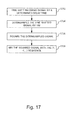
- FIG. 17 is a diagram illustrating an operational flow diagram for this transformation in accordance with one embodiment of the technology disclosed herein.
- FIG. 18 is a diagram illustrating a prior art transformation described by the Mehlan Reference.
- FIG. 19 illustrates an example computing module that may be used in implementing various features of embodiments of the disclosed technology.
- the technology disclosed herein in one embodiment is directed toward solutions to provide frequency and phase offset compensation.
- the technology may be directed toward solutions for symbol timing recovery, which can be implemented to determine symbol start time.
- systems and methods for performing nondata-aided digital feedforward estimation techniques are provided that can be implemented to continuously estimate and compensate for frequency and phase offset errors. Slow frequency offset drift can be tracked by embodiments of the technology disclosed herein, and embodiments can be used to recover symbol timing as well.
- Estimation techniques can be provided that do not require any knowledge of transmitted data and may be suitable for efficient implementation in digital circuits.
- Symbol timing recovery solutions can be provided to reduce correlator complexity and achieve more robust performance.
- a radio frequency receiver can be configured to receive a modulated signal transmitted across a channel, and it can include one or more transformation modules configured to generate a first error signal for an information signal representing the modulated signal received by the receiver.
- the transformation module can comprise a squaring module configured to square the information signal, thereby generating a squared signal, and a mixer configured to perform a complex multiplication of the squared signal by the local reference signal, and a downsampler configured to perform a spectrum folding of the mixed signal.
- the radio receiver can further include a symbol timing estimator module, configured to estimate a symbol timing of the receive signal based on the error signal generated by the transform module, and to generate a symbol timing signal; a frequency offset estimator module, configured to estimate a frequency offset of the received signal based on the error signal generated by the transform module; and a phase offset estimator module configured to estimate a phase error in the received signal based on the error signal generated by the transform module.
- the same transform module can be used to generate and supply the error signal(s) to the other modules, while in other embodiments, separate transform modules can be provided to generate the error signal(s) used by one or more of the other modules.
- a given transform module may comprise a plurality of separate transform modules to provide the error signals to their respective corresponding module or modules.
- a separate transform module is shown in each example of the frequency estimator, phase estimator, and symbol-timing estimator.
- the transformation can be used to extract the symbol timing, frequency and phase offsets of an MSK modulated signal.
- the transformation can be applied to other modulation schemes, including various forms of continuous phase modulation (CPM) schemes.
- CPM continuous phase modulation
- the example piece of equipment 300 includes a communication module 301 , a processor 306 (which can include multiple processors or processing units), and memory 310 (which can include memory units or modules of different types). These components are communicatively coupled via a bus 312 over which these modules may exchange and share information and other data.
- Communication module 301 includes wireless receiver module 302 , a wireless transmitter module 304 , and an I/O interface module 308 .
- An antenna 316 is coupled to wireless transmitter module 304 and is used by equipment 300 to transmit radio signals wirelessly to wireless equipment with which it is connected.
- These outbound RF signals can include information of almost any sort that is sent by equipment 300 to other entities.
- MFP multifunction peripheral
- this outbound information can include image files and related data (including metadata) sent by the camera to a computer, printer, or other device.
- Antenna 314 is included and coupled to wireless receiver module 302 to allow equipment 300 to receive signals from various wireless terminals within its reception range. Received signals can include information from other equipment used for operation of equipment 300 .
- inbound information received by wireless receiver module 302 can include, for example, files to be printed or faxed by the MFP.
- information received could be firmware updates, control information, or other information used by the camera.
- antennas are illustrated in this example, one of ordinary skill in the art will understand that various antenna and antenna configurations can be provided as can different quantities of antennas.
- transmit and receive functions can be accommodated using a common antenna or antenna structure, or separate antennas or antenna structures can be provided for transmit and receive functions as illustrated.
- antenna arrays or other groups of multiple antennas or antenna elements can be used for the transmit and receive functions.
- the wireless communications implemented using communication module 301 can be implemented according to a number of different wireless protocols, including standardized protocols. Examples of such standardized protocols include Bluetooth®, HiperLan, and various IEEE 802.11 communications standards, although other communication interfaces (whether or not standardized) can be implemented.
- An I/O interface module 308 is provided in the illustrated example, and can be configured to couple equipment 300 to other network nodes. These can include nodes or equipment.
- the I/O interface module 308 includes a receiver module 318 and a transmitter module 320 . Communications via the I/O interface module can be wired or wireless communications, and the transmitter and receiver contained therein can include line drivers and receivers, radios, antennas or other items, as may be appropriate for the given communication interfaces.
- Transmitter module 320 may be configured to transmit signals that can include voice, data and other communications. These may be sent in a standard network protocol if desired.
- Receiver module 318 is configured to receive signals from other equipment.
- I/O interface 308 can provide a hardwired complementary interface to the wireless interface described above. This may be, for example, an ethernet interface, a USB interface, a FireWire interface, or other hardwired interface.
- Memory 310 can be made up of one or more modules of one or more different types of memory, and in the illustrated example is configured to store data and other information 324 as well as operational instructions that may be used by the processor to operate equipment 300 .
- the processor 306 which can be implemented as one or more cores, CPUs, DSPs, or other processor units, for example, is configured to execute instructions or routines and to use the data and information in memory 310 in conjunction with the instructions to control the operation of the equipment 300 .
- image processing routines such as compression routines, can be stored in memory 310 and used by processor 306 to compress image files from raw files into JPEG files.
- modules can also be provided with the equipment 300 depending on the equipment's intended function or purpose. A complete list of various additional components and modules would be too lengthy to include, however a few examples are illustrative.
- a separate communication module 334 can also be provided for the equipment to manage and control communications received from other entities, and to direct received communications as appropriate.
- Communication module 334 can be configured to manage communication of various information sent to and received from other entities.
- Communication module 334 can be configured to manage both wired and wireless communications.
- control module 336 can be included to control the operation of equipment 300 .
- control module 336 can be configured to implement the features and functionality of equipment 300 .
- Functional modules 338 can also be included to provide equipment functionality.
- various modules (which may include various forms of hardware and software) can be provided to perform printing, scanning, faxing, and copying operations of the device.
- functional modules 338 can include modules such as, for example, optical systems, image capture modules, image processing modules, and so on. Again, as these examples illustrate, one of ordinary skill in the art will appreciate how other modules and components can be included with equipment 300 depending on the purpose or objectives of the equipment.
- FIG. 4 is a diagram illustrating a typical digital receiver with which the technology disclosed herein can be used in accordance with various embodiments.
- FIG. 5 is a flow diagram illustrating a typical operation of this example receiver.
- the incoming analog signal s IF (t) is centered at intermediate frequency f IF . Accordingly, the signal has been down converted to an intermediate frequency by an analog mixer (not shown).
- the intermediate frequency signal s IF (t) is sampled by analog-to-digital converter (ADC) 404 , placing the signal in the digital domain. The remainder of the processing is performed in the digital domain as indicated by the dashed box 406 .
- ADC analog-to-digital converter
- the sampled digital signal s IF (t) is downconverted into a complex baseband signal s(n).
- Baseband signal s(n) typically includes the information communicated from the transmitter to the receiver in the modulated signal and can thus be referred to as an information signal representing the modulated signal received by the receiver.
- the term information signal is not limited to describing a digital baseband signal, but can refer to other information signals whether digital or analog, baseband, IF or RF, or otherwise.
- s(n) Due to frequency mismatch between transmitter and receiver, s(n) has frequency offset from zero baseband frequency. That frequency offset produces an initial phase offset error and frequency offset error. These correspond to a phase and frequency offset in the modulated RF signal received by the receiver.
- symbol timing is not known on the receiver side due to digital and analog path delays. Therefore, the technology disclosed herein can be implemented to compensate for these phase and frequency errors and to find symbol timing.
- the digital receiver performs a symbol timing synchronization 410 , and at operation 508 frequency and offset phase compensation 412 .
- the corrected baseband signal s(n) is demodulated by demodulator 422 .
- a preamble correlator 420 can be implemented to detect, at operation 510 , the preamble sequence and identify the start of the frame.
- FIG. 6 is a diagram illustrating one example implementation for frequency and phase offset compensation with symbol timing recovery 400 in accordance with one embodiment of the technology described herein.
- This example implementation shown in FIG. 6 includes a delay block 602 , the symbol timing estimator 606 , a frequency/phase offset estimator 604 , a direct digital synthesizer (DDS) 608 , and a mixer 610 . Because this can be implemented in the digital domain, the phase and frequency offset compensation and symbol timing estimation can be accomplished using a processing system that may include, for example, digital signal processors executing program code or circuits to perform the described functions.
- DDS direct digital synthesizer
- frequency/phase offset estimator 604 can be configured to produce an estimate of the frequency offset ⁇ and/or phase estimate ⁇ of the Incoming signal. These ⁇ , ⁇ estimates can be used by direct digital synthesizer (DDS) 608 to generate a correction signal c(n ⁇ D). This correction signal c(n ⁇ D) can be applied at mixer 610 to remove the determined frequency and phase offsets. In the illustrated example, the correction signal c(n ⁇ D) is applied to a delayed version of received signal, s(n ⁇ D), which is created by delay module 602 . This delay D is used to compensate for processing time. A symbol trigger can be used to synchronize frequency/phase estimators with the received signal.
- DDS direct digital synthesizer
- Symbol timing estimator 606 can be used to generate a symbol trigger “sym trig” (e.g., a strobe) to indicate the start of a symbol. Accordingly, at the output is a phase/frequency corrected output signal 614 and a symbol timing signal, sym trig 616 .
- sym trig e.g., a strobe
- FIG. 7 is a diagram illustrating an example transformation that can be performed in accordance with various embodiments of the technology disclosed herein.
- FIG. 8 is an operational flow diagram illustrating a process performed by this transformation module.
- the modulated signal s(n) is received and squared by squaring module 704 . This results in a squared modulated signal s 2 (n).
- Direct digital synthesizer DDS 706 can be configured to, for example, generate, or synthesize, a frequency and phase-tunable output signal referenced to a frequency source.
- DDS 706 can be configured to generate a reference signal r(n), which is a complex exponential signal at two times the modulating frequency ⁇ .
- Reference signal r(n) can be reset by a system reset signal rst.
- the squared signal s 2 (n) is multiplied by the local reference signal r(n) using complex multiplier 708 , resulting in signal mix(n). That operation shifts spectrum components of squared signal by 2 ⁇ .
- the signal mix(n) is time shifted or delayed, which can be accomplished using a shift register 710 with a delay input D.
- the signal can be shifted by D (0 ⁇ D ⁇ M), resulting in time-shifted signal mix(n ⁇ D).
- delay input D is generated from sym trig 616 , for example, as described below with reference to FIG. 9 .
- downsampling is accomplished using downsampler 712 to produce error signal e(m) at the output, where f S is a sampling frequency and R is a symbol rate.
- f S is a sampling frequency
- R is a symbol rate.
- f IF f S /4
- f S 8R
- ⁇ ⁇ 2 ⁇ T is the modulating frequency
- i and M are a fraction of the symbol time 0 ⁇ i ⁇ M and the symbol oversampling rate M, respectively;
- ⁇ is the timing error relative to T, 0.5 ⁇ 0.5;
- ⁇ and ⁇ 0 are the frequency offset error and initial phase error, respectively.
- the squaring operation which in this case is nonlinear, produces the signal as shown in Eq. (2).
- three blocks or modules provided herein include a symbol timing generator, a frequency estimator frequency estimator and a phase estimator.
- An example of these in combination is shown in FIG. 6 , in which the symbol timing estimator is shown at 606 , and the frequency and phase offset estimator is shown at 604 . Examples of these blocks are now described.
- FIG. 9 is a diagram illustrating an example block for performing frequency estimation in accordance with various embodiments of the technology disclosed herein.
- FIG. 10 is an operational flow diagram illustrating an example process for frequency estimation in accordance with various embodiments of the technology disclosed herein.
- the example frequency estimator includes a transform block 902 , a filtering block 904 , a conjugate/delay block 906 , a mixer 908 , a CORDIC 910 , a divider 912 , low pass filter 914 and converter 916 .
- the modulated signal e.g. an MSK modulated signal
- s(n) is received by the frequency estimator.
- transform module 902 applies a transform, which can be keyed based on a sym trig (e.g., sym trig 616 ).
- That symbol trigger signal can be converted into delay D by converter 916 for transform 902 .
- the conversion can be accomplished, for example, by determining which of M clocks contains a symbol trigger set to one.
- the resultant delay D (0 ⁇ D ⁇ M) is provided to transform 902 .
- low pass filter block 904 filters the signal to remove high-frequency noise, resulting in filtered error signal e′(m).
- conjugate/delay block 906 conjugate and delays the transformed filtered signal, and at operation 1008 the transform signal and the delayed transformed signal are multiplied at mixer 908 to determine the phase difference between two consecutive samples.
- CORDIC block 910 extracts the phase. In some embodiments, this is accomplished by converting from x,y coordinates to polar coordinates (amplitude and phase) to determine the phase differential by other methods. Accordingly, this results in signal 2M ⁇ (m). This signal, is 2M larger due to the squaring and downsampling that occur in the transform (see FIG. 7 for example). Accordingly, at operation 1012 , the frequency offset is divided by 2M and the system produces an instantaneous estimate of frequency error ⁇ (m). After that at operation 1014 , the estimator estimates a mean of the frequency error. In one embodiment, this can be accomplished using a low pass filter 914 , which can be implemented as an infinite impulse response (IIR) filter or finite impulse response (FIR) filter. This can be implemented to continuously track the mean of the frequency error ⁇ est (m).
- IIR infinite impulse response
- FIR finite impulse response
- the system can also be configured to determine the phase offset. After the system performs a frequency offset determination, the determined frequency may still have some mismatch to the true frequency. Any such mismatch will result in a phase error that accumulates over time. Therefore, the system can be configured to not only estimate the initial phase, but also to estimate the residual phase error resulting from frequency offset mismatch.
- FIG. 11 is a diagram illustrating an example of a phase estimator block for estimating residual phase error in accordance with one embodiment of the technology described herein.
- FIG. 12 is an operational flow diagram illustrating an example process for phase offset estimation in accordance with one embodiment of the technology described herein. Referring now to FIGS. 11 and 12 , at operation 1202 the phase estimator block applies transform 1102 .
- transform 1102 One example of a transform 1102 they can be applied is the transform described above with reference to FIG. 7 .
- the transformed signal e(m) is filtered by filter 1104 .
- Filter 1104 can be configured to average instantaneous phase errors prior to phase extraction using CORDIC 1106 .
- this operation can be performed using a simple LMS-like (least mean square) adaptive filter, or other type of filter that is capable of estimating an average of the instantaneous phases.
- filtering is performed before the CORDIC, because the CORDIC produces ⁇ to ⁇ phase, and noise will cause this output to wrap the instantaneous phase.
- the mean of the phase offset is extracted. In some embodiments, this can be performed by a CORDIC operation.
- the CORDIC 1106 produces two times the phase error ⁇ (m) that can be unwrapped using simple logic.
- the estimator unwraps this phase error to track the accumulated phase offset. Because there is a residual phase offset, the phase ultimately wraps at ⁇ or ⁇ points (the phase of complex numbers defined from ⁇ to ⁇ ).
- the estimator divides by two to determine the phase estimate. Division by two after unwrapping gives phase error ⁇ est (m) of interest.
- Symbol timing recovery is used to determine the timing, or clock of the transmitted symbols.
- the system can be configured to take the incoming signal and set different delays, D from 0 to M ⁇ 1, and to apply these as transform delays.
- a polyphase dock can be used to provide multiple phases to the delay blocks to apply the different delays.
- the output of this block is used to generate symbol trigger signal “sym trig” for the frequency/phase estimator so that it may synchronize the received signal with the local reference free running DDS, which may be reset by some arbitrary reset signal “rst”.
- FIG. 13 is a diagram illustrating an example block for performing symbol timing recovery in accordance with various embodiments of the technology disclosed herein.
- FIG. 14 is an operational flow diagram illustrating an example process for symbol timing recovery in accordance with various embodiments of the technology disclosed herein.
- the example shows a plurality of delays 1302 .
- the example symbol timing estimator block shown in FIG. 13 recovers symbol timing information with 1/M clock precision.
- the time-shift value D of each transform unit is equal to 0 . . . M ⁇ 1.
- low pass filters can be employed to filter out high frequency noise, and they can be implemented as an IIR or other appropriate low pass filter. This can be useful, for example, to remove the additive white Gaussian noise (AWGN) on the signal.
- AWGN additive white Gaussian noise
- the instantaneous power of the filtered error signal is calculated. This is performed by blocks 1306 .
- the symbol timing estimator determines the mean power by low pass filtering instantaneous power.
- low pass filters are implemented as FIR filters or IIR filters to find the mean power.
- the maximum power signal is selected to determine symbol timing.
- a comparator 1310 can be used to compare the mean power from each of the related branches to determine which one has the maximum power. The system selects the branch with the maximum power, and its associated delay is identified. The maximum power output points out the delay D between the received signal and local reference signal to recover symbol timing.
- docks at different phases are used to trigger delay transforms 1302 .
- FIG. 15 is a block diagram illustrating an example architecture of a system for frequency and phase estimation with symbol timing recovery in accordance with one embodiment of the technology described herein.
- an example implementation includes a delay blocks 1502 , 1510 , a frequency offset estimator 1504 , a symbol timing estimator 1506 , a DDS 1508 , mixers 1516 and 1518 , a phase-offset estimator 1512 , and a DDS block 1514 .
- frequency offset estimation 1504 and phase offset estimation 1512 can be performed separately. Particularly, in this example, frequency offset estimation is performed before phase offset estimation.
- symbol timing estimation can be used to generate the trigger signal sym trig that is used to trigger frequency-offset estimator 1504 and phase-offset estimator 1512 .
- frequency offset estimator 1504 can be implemented, for example, using frequency offset estimator 900 as described above.
- DDS 1508 can be configured to provide the appropriate correction signal to make sure 1518 to remove the frequency offset. Because there may still be some frequency mismatch, phase offset estimator 1512 can be used to remove any additional phase offset created by this mismatch.
- phase offset estimator 1512 can be implemented, for example, using phase offset estimator 1100 as described above. Phase offset estimator 1512 can be configured to output an estimate of the phase offset to DDS 1514 such that mixer 1516 can apply the correction removing the phase offset from the signal.
- FIG. 16 is a block diagram illustrating another example transformation in accordance with one embodiment of the technology disclosed herein.
- FIG. 17 is a diagram illustrating an operational flow diagram for this transformation in accordance with one embodiment of the technology disclosed herein. Referring now to FIGS. 16 and 17 , at operation 1702 the incoming signal s(n) is time shifted or delayed. In this example, a shift register 1604 is provided at the beginning of the transformation to introduce delay into the incoming signal s(n), resulting in delayed signal s(n ⁇ D).
- the signal s(n) can be shifted by D (0 ⁇ D ⁇ M), resulting in time-shifted signal s(n ⁇ D).
- Time shifting the signal with shift register provides the opportunity to select which sample from a stream of samples is chosen by the downsampling (discussed below).
- downsampling is accomplished by downsampling block 1606 to produce downsampled signal s(m) at the output.
- the downsampled the signal is squared by block 1608 . This results in the squared downsampled signal s 2 (m).
- mixer 1612 is used to combine the squared output s 2 (m) with r(m) from the DDS 1610 . This can be done by a complex multiplication of the two signals.
- reference signal r(m) is at f s /2, therefore, the DDS 1610 can be simplified to [1, ⁇ 1, . . . ] real-valued sequence and hence complex multiplication replaced by two real multiplications with a [1, ⁇ 1 . . . ] sequence.
- the Mehlan transformation 1800 includes operations of shifting the incoming signal and downsampling the shifted signal as illustrated at blocks 1802 and 1804 . Then, the transformation 1800 multiplies (through complex multiplication) the downsampled signal s(m) with the delayed conjugate of the signal, s*(m ⁇ 1), produced by conjugate/delay block 1806 . The resultant signal, c(m), is then squared by block 1808 . This is in contrast to the embodiments described above in which the squaring is performed before multiplication by the DDS output.
- module might describe a given unit of functionality that can be performed in accordance with one or more embodiments of the technology disclosed herein.
- a module might be implemented utilizing any form of hardware, software, or a combination thereof.
- processors, controllers, ASICs, PLAs, PALs, CPLDs, FPGAs, logical components, software routines or other mechanisms might be implemented to make up a module.
- the various modules described herein might be implemented as discrete modules or the functions and features described can be shared in part or in total among one or more modules.
- FIG. 19 One such example computing module is shown in FIG. 19 .
- FIG. 19 Various embodiments are described in terms of this example-computing module 1900 . After reading this description, it will become apparent to a person skilled in the relevant art how to implement the technology using other computing modules or architectures.
- computing module 1900 may represent, for example, computing or processing capabilities found within desktop, laptop and notebook computers; hand-held computing devices (PDA's, smart phones, cell phones, palmtops, etc.); mainframes, supercomputers, workstations or servers; or any other type of special-purpose or general-purpose computing devices as may be desirable or appropriate for a given application or environment.
- Computing module 1900 might also represent computing capabilities embedded within or otherwise available to a given device.
- a computing module might be found in other electronic devices such as, for example, digital cameras, navigation systems, cellular telephones, portable computing devices, modems, routers, WAPs, terminals and other electronic devices that might include some form of processing capability.
- Computing module 1900 might include, for example, one or more processors, controllers, control modules, or other processing devices, such as a processor 1904 .
- Processor 1904 might be implemented using a general-purpose or special-purpose processing engine such as, for example, a microprocessor, controller, or other control logic.
- processor 1904 is connected to a bus 1902 , although any communication medium can be used to facilitate interaction with other components of computing module 1900 or to communicate externally.
- Computing module 1900 might also include one or more memory modules, simply referred to herein as main memory 1908 .
- main memory 1908 preferably random access memory (RAM) or other dynamic memory, might be used for storing information and instructions to be executed by processor 1904 .
- Main memory 1908 might also be used for storing temporary variables or other intermediate information during execution of instructions to be executed by processor 1904 .
- Computing module 1900 might likewise include a read only memory (“ROM”) or other static storage device coupled to bus 1902 for storing static information and instructions for processor 1904 .
- ROM read only memory
- the computing module 1900 might also include one or more various forms of information storage mechanism 1910 , which might include, for example, a media drive 1912 and a storage unit interface 1920 .
- the media drive 1912 might include a drive or other mechanism to support fixed or removable storage media 1914 .
- a hard disk drive, a floppy disk drive, a magnetic tape drive, an optical disk drive, a CD or DVD drive (R or RW), or other removable or fixed media drive might be provided.
- storage media 1914 might include, for example, a hard disk, a floppy disk, magnetic tape, cartridge, optical disk, a CD or DVD, or other fixed or removable medium that is read by, written to or accessed by media drive 1912 .
- the storage media 1914 can include a computer usable storage medium having stored therein computer software or data.
- information storage mechanism 1910 might include other similar instrumentalities for allowing computer programs or other instructions or data to be loaded into computing module 1900 .
- Such instrumentalities might include, for example, a fixed or removable storage unit 1922 and an interface 1920 .
- Examples of such storage units 1922 and interfaces 1920 can include a program cartridge and cartridge interface, a removable memory (for example, a flash memory or other removable memory module) and memory slot, a PCMCIA slot and card, and other fixed or removable storage units 1922 and interfaces 1920 that allow software and data to be transferred from the storage unit 1922 to computing module 1900 .
- Computing module 1900 might also include a communications interface 1924 .
- Communications interface 1924 might be used to allow software and data to be transferred between computing module 1900 and external devices.
- Examples of communications interface 1924 might include a modem or softmodem, a network interface (such as an Ethernet, network interface card, WiMedia, IEEE 802.XX or other interface), a communications port (such as for example, a USB port, IR port, RS232 port Bluetooth® interface, or other port), or other communications interface.
- Software and data transferred via communications interface 1924 might typically be carried on signals, which can be electronic, electromagnetic (which includes optical) or other signals capable of being exchanged by a given communications interface 1924 . These signals might be provided to communications interface 1924 via a channel 1928 .
- This channel 1928 might carry signals and might be implemented using a wired or wireless communication medium.
- Some examples of a channel might include a phone line, a cellular link, an RF link, an optical link, a network interface, a local or wide area network, and other wired or wireless communications channels.
- computer program medium and “computer usable medium” are used to generally refer to media such as, for example, memory 1908 , storage unit 1920 , media 1914 , and channel 1928 .
- These and other various forms of computer program media or computer usable media may be involved in carrying one or more sequences of one or more instructions to a processing device for execution.
- Such instructions embodied on the medium are generally referred to as “computer program code” or a “computer program product” (which may be grouped in the form of computer programs or other groupings). When executed, such instructions might enable the computing module 1900 to perform features or functions of the disclosed technology as discussed herein.
- module does not imply that the components or functionality described or claimed as part of the module are all configured in a common package. Indeed, any or all of the various components of a module, whether control logic or other components, can be combined in a single package or separately maintained and can further be distributed in multiple groupings or packages or across multiple locations.
Abstract
Description
E{e(m)}=(1+cos 2πε))e 2jΔwT
data bit of modulating data sequence akε(0,1);
is the result of an exclusive OR inverse operation that depends on both even and odd bits;
is the modulating frequency;
at
E{e(m)}=(1+cos 2πε))e 2jΔwT.
Whereas, in contrast, in embodiments described herein, the error signal is
e(m)=e 2j{(−1)
in which the ε component represents the symbol timing, the Δω component represents the frequency offset estimate, and the θ0 component represents the phase offset.
Claims (23)
e(m)=e 2j|(−1)
e(m)=e 2j|(−1)
Priority Applications (5)
| Application Number | Priority Date | Filing Date | Title |
|---|---|---|---|
| US14/229,761 US9270390B2 (en) | 2014-03-28 | 2014-03-28 | Frequency and phase offset compensation of modulated signals with symbol timing recovery |
| DE112015001066.1T DE112015001066T5 (en) | 2014-03-28 | 2015-02-25 | Frequency and phase offset compensation of modulated signals with symbol clock recovery |
| JP2016570939A JP2017513417A (en) | 2014-03-28 | 2015-02-25 | Frequency and phase offset compensation to recover code timing of modulated signal |
| PCT/US2015/017580 WO2015148036A1 (en) | 2014-03-28 | 2015-02-25 | Frequency and phase offset compensation of modulated signals with symbol timing recovery |
| CN201580016345.9A CN106165366B (en) | 2014-03-28 | 2015-02-25 | Frequency and phase offset compensation are carried out to modulated signal using symbol timing recovery |
Applications Claiming Priority (1)
| Application Number | Priority Date | Filing Date | Title |
|---|---|---|---|
| US14/229,761 US9270390B2 (en) | 2014-03-28 | 2014-03-28 | Frequency and phase offset compensation of modulated signals with symbol timing recovery |
Publications (2)
| Publication Number | Publication Date |
|---|---|
| US20150280841A1 US20150280841A1 (en) | 2015-10-01 |
| US9270390B2 true US9270390B2 (en) | 2016-02-23 |
Family
ID=52672335
Family Applications (1)
| Application Number | Title | Priority Date | Filing Date |
|---|---|---|---|
| US14/229,761 Expired - Fee Related US9270390B2 (en) | 2014-03-28 | 2014-03-28 | Frequency and phase offset compensation of modulated signals with symbol timing recovery |
Country Status (5)
| Country | Link |
|---|---|
| US (1) | US9270390B2 (en) |
| JP (1) | JP2017513417A (en) |
| CN (1) | CN106165366B (en) |
| DE (1) | DE112015001066T5 (en) |
| WO (1) | WO2015148036A1 (en) |
Cited By (1)
| Publication number | Priority date | Publication date | Assignee | Title |
|---|---|---|---|---|
| US20230179452A1 (en) * | 2020-04-28 | 2023-06-08 | Lg Electronics Inc. | Signal processing device and image display apparatus including the same |
Families Citing this family (29)
| Publication number | Priority date | Publication date | Assignee | Title |
|---|---|---|---|---|
| US10123362B2 (en) * | 2013-12-18 | 2018-11-06 | Telefonaktiebolaget Lm Ericsson (Publ) | Operation of a multi-standard base station site supporting at least two different radio access technologies |
| US10382246B2 (en) * | 2014-01-07 | 2019-08-13 | Quantumsine Acquisitions Inc. | Combined amplitude-time and phase modulation |
| US11140018B2 (en) * | 2014-01-07 | 2021-10-05 | Quantumsine Acquisitions Inc. | Method and apparatus for intra-symbol multi-dimensional modulation |
| US9722833B2 (en) * | 2015-04-29 | 2017-08-01 | Texas Instruments Incorporated | Circuits and methods for frequency offset estimation in FSK communications |
| KR102517583B1 (en) | 2015-06-26 | 2023-04-03 | 칸도우 랩스 에스에이 | High speed communications system |
| KR101817544B1 (en) * | 2015-12-30 | 2018-01-11 | 어보브반도체 주식회사 | Bluetooth signal receiving method and device using improved carrier frequency offset compensation |
| WO2018004180A1 (en) * | 2016-06-27 | 2018-01-04 | 엘지전자 주식회사 | Method for transmitting and receiving reference signal in wireless communication system and device therefor |
| WO2018070998A1 (en) * | 2016-10-11 | 2018-04-19 | Halliburton Energy Services, Inc. | Calibrating a digital telemetry system |
| JP6772048B2 (en) * | 2016-12-14 | 2020-10-21 | ルネサスエレクトロニクス株式会社 | Rate judgment device, rate judgment method and receiver |
| US10296831B2 (en) | 2017-05-03 | 2019-05-21 | Virginia Tech Intellectual Properties, Inc. | Learning radio signals using radio signal transformers |
| CN110945830B (en) * | 2017-05-22 | 2022-09-09 | 康杜实验室公司 | Multimode data driven clock recovery circuit |
| KR102347396B1 (en) | 2017-12-28 | 2022-01-04 | 칸도우 랩스 에스에이 | Synchronously Switched Multi-Input Demodulating Comparator |
| US10790920B2 (en) | 2018-12-21 | 2020-09-29 | Kratos Integral Holdings, Llc | System and method for processing signals using feed forward carrier and timing recovery |
| US11571184B2 (en) * | 2019-04-03 | 2023-02-07 | Bfly Operations, Inc. | Ultrasound device with elevational beamforming |
| IT201900005706A1 (en) * | 2019-04-12 | 2020-10-12 | Univ Degli Studi Milano | Method and system of transmission and reception of an electromagnetic radiation beam with orbital angular momentum detection and related method and telecommunication system |
| US11529127B2 (en) * | 2019-06-25 | 2022-12-20 | Bfly Operations, Inc. | Methods and apparatuses for processing ultrasound signals |
| CN111294302A (en) * | 2020-02-07 | 2020-06-16 | 中国人民解放军空军研究院战略预警研究所 | Synchronization method, device, equipment and storage medium of MSK modulation signal |
| CN112448905B (en) * | 2020-11-12 | 2021-08-31 | 四川九洲电器集团有限责任公司 | Demodulation system and demodulation method for MSK digital baseband signal |
| US11743852B2 (en) * | 2020-11-30 | 2023-08-29 | Silicon Laboratories Inc. | Phase measurements for high accuracy distance measurements |
| US11431359B2 (en) | 2020-11-30 | 2022-08-30 | Silicon Laboratories Inc. | DC offset compensation in zero-intermediate frequency mode of a receiver |
| US11737038B2 (en) * | 2020-11-30 | 2023-08-22 | Silicon Laboratories Inc. | Correction of frequency offset between initiator and reflector |
| US11438200B2 (en) | 2020-11-30 | 2022-09-06 | Silicon Laboratories Inc. | Frequency offset compensation at reflector during frequency compensation interval |
| US11638116B2 (en) | 2020-12-01 | 2023-04-25 | Silicon Laboratories Inc. | Adjusting DFT coefficients to compensate for frequency offset during a sounding sequence used for fractional time determination |
| US11502883B2 (en) | 2020-12-01 | 2022-11-15 | Silicon Laboratories Inc. | Adjusting receiver frequency to compensate for frequency offset during a sounding sequence used for fractional time determination |
| CN112600520A (en) * | 2020-12-08 | 2021-04-02 | 上海擎昆信息科技有限公司 | Parallel digital frequency conversion method, system and storage medium |
| IL308837A (en) | 2021-05-24 | 2024-01-01 | Kratos Integral Holdings Llc | Systems and methods for post-detect combining of a plurality of downlink signals representative of a communication signal |
| US11632733B2 (en) | 2021-09-13 | 2023-04-18 | Silicon Laboratories Inc. | System, apparatus and method for acquisition of signals in wireless systems with adverse oscillator variations |
| US11864141B2 (en) * | 2021-11-29 | 2024-01-02 | National Institute Of Information And Communications Technology | Wireless communication system performing mutual wireless communication between terminals to perform time difference measurement and propagation time measurement |
| CN114826415B (en) * | 2022-04-01 | 2023-11-17 | 北京航空航天大学 | Spiral driving signal modulation device and method and imaging system |
Citations (7)
| Publication number | Priority date | Publication date | Assignee | Title |
|---|---|---|---|---|
| US4384357A (en) | 1981-04-03 | 1983-05-17 | Canadian Patens & Development Limited | Self-synchronization circuit for a FFSK or MSK demodulator |
| US5111479A (en) * | 1989-11-02 | 1992-05-05 | Clarion Co., Ltd. | Spread spectrum receiver and carrier sense circuit therefor |
| US5535249A (en) | 1994-07-06 | 1996-07-09 | Nec Corporation | Precise detection of frequency error for bursts modulated by predetermined symbol sequence |
| US5867059A (en) | 1995-06-22 | 1999-02-02 | National Science Council | Demodulating system for MSK and GMSK signal using a fast fourier transform converter |
| US20030235257A1 (en) | 2002-06-20 | 2003-12-25 | Seung-Hwan Lee | Apparatus and method for receiving digital signal |
| US7630428B2 (en) | 2005-07-28 | 2009-12-08 | Itt Manufacturing Enterprises, Inc. | Fast digital carrier frequency error estimation algorithm using synchronization sequence |
| US20130170576A1 (en) * | 2011-12-30 | 2013-07-04 | John Qingchong Liu | Assembly and Method for Detecting Multiple Level Signals |
Family Cites Families (8)
| Publication number | Priority date | Publication date | Assignee | Title |
|---|---|---|---|---|
| JPH07202964A (en) * | 1993-12-28 | 1995-08-04 | Uchu Tsushin Kiso Gijutsu Kenkyusho:Kk | Batch storage demodulator for k phase psk modulated signal |
| US6430235B1 (en) * | 1998-11-05 | 2002-08-06 | Wireless Facilities, Inc. | Non-data-aided feedforward timing synchronization method |
| JP3544147B2 (en) * | 1999-05-31 | 2004-07-21 | 株式会社東芝 | OFDM signal receiving apparatus, OFDM signal communication system and communication control method therefor |
| KR100458630B1 (en) * | 2002-10-07 | 2004-12-03 | 광주과학기술원 | Method and Apparatus for Joint Phase Offset and Frequency Offset Estimator for MPSK Transmission |
| JP4585455B2 (en) * | 2006-01-20 | 2010-11-24 | 富士通セミコンダクター株式会社 | Demodulation circuit and demodulation method |
| JP4872651B2 (en) * | 2006-12-20 | 2012-02-08 | ソニー株式会社 | Wireless communication apparatus and wireless communication method |
| CN101442364B (en) * | 2007-11-19 | 2011-10-19 | 富士通株式会社 | Light coherent receiver, frequency difference estimation apparatus and method for light coherent receiver |
| US8625726B2 (en) * | 2011-09-15 | 2014-01-07 | The Boeing Company | Low power radio frequency to digital receiver |
-
2014
- 2014-03-28 US US14/229,761 patent/US9270390B2/en not_active Expired - Fee Related
-
2015
- 2015-02-25 WO PCT/US2015/017580 patent/WO2015148036A1/en active Application Filing
- 2015-02-25 CN CN201580016345.9A patent/CN106165366B/en active Active
- 2015-02-25 DE DE112015001066.1T patent/DE112015001066T5/en not_active Withdrawn
- 2015-02-25 JP JP2016570939A patent/JP2017513417A/en active Pending
Patent Citations (7)
| Publication number | Priority date | Publication date | Assignee | Title |
|---|---|---|---|---|
| US4384357A (en) | 1981-04-03 | 1983-05-17 | Canadian Patens & Development Limited | Self-synchronization circuit for a FFSK or MSK demodulator |
| US5111479A (en) * | 1989-11-02 | 1992-05-05 | Clarion Co., Ltd. | Spread spectrum receiver and carrier sense circuit therefor |
| US5535249A (en) | 1994-07-06 | 1996-07-09 | Nec Corporation | Precise detection of frequency error for bursts modulated by predetermined symbol sequence |
| US5867059A (en) | 1995-06-22 | 1999-02-02 | National Science Council | Demodulating system for MSK and GMSK signal using a fast fourier transform converter |
| US20030235257A1 (en) | 2002-06-20 | 2003-12-25 | Seung-Hwan Lee | Apparatus and method for receiving digital signal |
| US7630428B2 (en) | 2005-07-28 | 2009-12-08 | Itt Manufacturing Enterprises, Inc. | Fast digital carrier frequency error estimation algorithm using synchronization sequence |
| US20130170576A1 (en) * | 2011-12-30 | 2013-07-04 | John Qingchong Liu | Assembly and Method for Detecting Multiple Level Signals |
Non-Patent Citations (6)
| Title |
|---|
| Efstathiou D. et al: Feedforward Synchronisation Techniques for 16-QAM TDMA Demodulators, Global Telecommunications Conference, 1996. Globecom '96. Communications: The Key to Global Prosperity London, UK Nov. 18-22, 1996, New York, NY, US, IEEE, vol. 2, Nov. 18, 1996, pp. 1432-1436. |
| International Search Report and the Written Opinion for International App No. PCT/US2015/017580, mailed May 18, 2015. |
| Lambrette, U. et al: Two timing recovery algorithms for MSK, Communications, 1994, ICC '94, Supercomm/ICC '94, Conference Record, Serving Humanity Through Communications, IEEE International Conference on, May 1-5, 1994, pp. 1155-1159. |
| Mehlan, R.: A Fully Digital Feedforward MSK Demodulator with Joint Frequency Offset and Symbol Timing Estimation for Burst Mode Mobile Radio, Vehicular Technology, IEEE Transactions on, Nov. 1993, pp. 434-443. |
| Pasupathy, S.: Minimum shift keying: A spectrally efficient modulation, Communications Magazine, IEEE, Jul. 1979, pp. 14-22. |
| Seung Joon Lee et al: Performance Improvement of Non-Data-Aided Feedforward Symbol Timing Estimation Using the Better Than Raised-Cosine Pulse, IEEE Transactions on Communications, vol. 56, No. 4, Apr. 1, 2008, pp. 542-544. |
Cited By (1)
| Publication number | Priority date | Publication date | Assignee | Title |
|---|---|---|---|---|
| US20230179452A1 (en) * | 2020-04-28 | 2023-06-08 | Lg Electronics Inc. | Signal processing device and image display apparatus including the same |
Also Published As
| Publication number | Publication date |
|---|---|
| CN106165366B (en) | 2019-08-02 |
| DE112015001066T5 (en) | 2016-12-01 |
| JP2017513417A (en) | 2017-05-25 |
| CN106165366A (en) | 2016-11-23 |
| US20150280841A1 (en) | 2015-10-01 |
| WO2015148036A1 (en) | 2015-10-01 |
Similar Documents
| Publication | Publication Date | Title |
|---|---|---|
| US9270390B2 (en) | Frequency and phase offset compensation of modulated signals with symbol timing recovery | |
| US10516521B2 (en) | Sampling rate synchronization between transmitters and receivers | |
| JP2643792B2 (en) | Demodulator | |
| US5787123A (en) | Receiver for orthogonal frequency division multiplexed signals | |
| US6055281A (en) | Passband DQPSK detector for a digital communications receiver | |
| WO1998023070A9 (en) | Passband dqpsk detector for a digital communications receiver | |
| JPH0746218A (en) | Digital demodulator | |
| CN110300079B (en) | MSK signal coherent demodulation method and system | |
| US4518922A (en) | Decision-directed, automatic frequency control technique for non-coherently demodulated M-ARY frequency shift keying | |
| JP4165413B2 (en) | Radio data communication demodulator and demodulation method | |
| US9912512B2 (en) | Systems and methods for frequency synchronization between transmitters and receivers in a communication system | |
| KR100487328B1 (en) | Apparatus for recovering carrier | |
| US20170288922A1 (en) | Frequency estimation and tracking in a receiver | |
| CN111049636B (en) | BPSK bit synchronization device and method | |
| US9912511B2 (en) | Systems and methods for time synchronization between transmitters and receivers in a communication system | |
| KR101645861B1 (en) | Synchronous demodulator electronic circuit for phase modulation signals | |
| EP1693954B1 (en) | Demodulation circuit for use in receiver using IF sampling scheme | |
| KR100594269B1 (en) | A frequency phase locked loop circuit and a Advanced Television Systems Committee Digital Television demodulator using the same. | |
| CN115118564A (en) | Carrier frequency deviation estimation method and device | |
| JP4098745B2 (en) | Digital demodulator | |
| JP4129530B2 (en) | Carrier synchronization method | |
| JP2003169101A (en) | Signal demodulator and signal demodulating method | |
| CN115883302A (en) | Load phase tracking method, device and medium based on training sequence | |
| JP3394276B2 (en) | AFC circuit | |
| JP4803079B2 (en) | Demodulator |
Legal Events
| Date | Code | Title | Description |
|---|---|---|---|
| AS | Assignment |
Owner name: OLYMPUS COMMUNICATION TECHNOLOGY OF AMERICA, INC., Free format text: ASSIGNMENT OF ASSIGNORS INTEREST;ASSIGNORS:GUDOVSKIY, DENIS A.;CHU, LICHUNG;REEL/FRAME:033076/0768 Effective date: 20140529 Owner name: OLYMPUS CORPORATION, JAPAN Free format text: ASSIGNMENT OF ASSIGNORS INTEREST;ASSIGNOR:OLYMPUS COMMUNICATION TECHNOLOGY OF AMERICA, INC.;REEL/FRAME:033077/0120 Effective date: 20140529 |
|
| ZAAA | Notice of allowance and fees due |
Free format text: ORIGINAL CODE: NOA |
|
| ZAAB | Notice of allowance mailed |
Free format text: ORIGINAL CODE: MN/=. |
|
| STCF | Information on status: patent grant |
Free format text: PATENTED CASE |
|
| AS | Assignment |
Owner name: OLYMPUS CORPORATION, JAPAN Free format text: CHANGE OF ADDRESS;ASSIGNOR:OLYMPUS CORPORATION;REEL/FRAME:039344/0502 Effective date: 20160401 |
|
| MAFP | Maintenance fee payment |
Free format text: PAYMENT OF MAINTENANCE FEE, 4TH YEAR, LARGE ENTITY (ORIGINAL EVENT CODE: M1551); ENTITY STATUS OF PATENT OWNER: LARGE ENTITY Year of fee payment: 4 |
|
| FEPP | Fee payment procedure |
Free format text: MAINTENANCE FEE REMINDER MAILED (ORIGINAL EVENT CODE: REM.); ENTITY STATUS OF PATENT OWNER: LARGE ENTITY |
|
| LAPS | Lapse for failure to pay maintenance fees |
Free format text: PATENT EXPIRED FOR FAILURE TO PAY MAINTENANCE FEES (ORIGINAL EVENT CODE: EXP.); ENTITY STATUS OF PATENT OWNER: LARGE ENTITY |
|
| STCH | Information on status: patent discontinuation |
Free format text: PATENT EXPIRED DUE TO NONPAYMENT OF MAINTENANCE FEES UNDER 37 CFR 1.362 |