US9299786B2 - Semiconductor device - Google Patents
Semiconductor device Download PDFInfo
- Publication number
- US9299786B2 US9299786B2 US14/824,512 US201514824512A US9299786B2 US 9299786 B2 US9299786 B2 US 9299786B2 US 201514824512 A US201514824512 A US 201514824512A US 9299786 B2 US9299786 B2 US 9299786B2
- Authority
- US
- United States
- Prior art keywords
- sectional
- taken along
- along line
- sidewall
- cross
- Prior art date
- Legal status (The legal status is an assumption and is not a legal conclusion. Google has not performed a legal analysis and makes no representation as to the accuracy of the status listed.)
- Active
Links
- 239000004065 semiconductor Substances 0.000 title claims abstract description 78
- 229910052710 silicon Inorganic materials 0.000 claims abstract description 81
- 239000010703 silicon Substances 0.000 claims abstract description 81
- 239000010410 layer Substances 0.000 description 114
- XUIMIQQOPSSXEZ-UHFFFAOYSA-N Silicon Chemical compound [Si] XUIMIQQOPSSXEZ-UHFFFAOYSA-N 0.000 description 77
- 238000009792 diffusion process Methods 0.000 description 51
- 229910021420 polycrystalline silicon Inorganic materials 0.000 description 48
- 229920005591 polysilicon Polymers 0.000 description 48
- 238000004519 manufacturing process Methods 0.000 description 45
- 238000000034 method Methods 0.000 description 44
- 238000005530 etching Methods 0.000 description 17
- 150000004767 nitrides Chemical class 0.000 description 16
- 229910052751 metal Inorganic materials 0.000 description 14
- 239000002184 metal Substances 0.000 description 14
- 230000003247 decreasing effect Effects 0.000 description 12
- 229910021332 silicide Inorganic materials 0.000 description 12
- FVBUAEGBCNSCDD-UHFFFAOYSA-N silicide(4-) Chemical compound [Si-4] FVBUAEGBCNSCDD-UHFFFAOYSA-N 0.000 description 11
- 239000012535 impurity Substances 0.000 description 9
- 230000010354 integration Effects 0.000 description 6
- 239000000758 substrate Substances 0.000 description 6
- 239000011229 interlayer Substances 0.000 description 5
- 239000000463 material Substances 0.000 description 5
- ZOXJGFHDIHLPTG-UHFFFAOYSA-N Boron Chemical compound [B] ZOXJGFHDIHLPTG-UHFFFAOYSA-N 0.000 description 3
- 229910052785 arsenic Inorganic materials 0.000 description 3
- RQNWIZPPADIBDY-UHFFFAOYSA-N arsenic atom Chemical compound [As] RQNWIZPPADIBDY-UHFFFAOYSA-N 0.000 description 3
- 229910052796 boron Inorganic materials 0.000 description 3
- 239000000969 carrier Substances 0.000 description 3
- 238000010438 heat treatment Methods 0.000 description 3
- 238000000151 deposition Methods 0.000 description 2
- 238000005468 ion implantation Methods 0.000 description 2
- RTAQQCXQSZGOHL-UHFFFAOYSA-N Titanium Chemical compound [Ti] RTAQQCXQSZGOHL-UHFFFAOYSA-N 0.000 description 1
- NRTOMJZYCJJWKI-UHFFFAOYSA-N Titanium nitride Chemical compound [Ti]#N NRTOMJZYCJJWKI-UHFFFAOYSA-N 0.000 description 1
- 230000007423 decrease Effects 0.000 description 1
- 150000002500 ions Chemical class 0.000 description 1
- 239000007769 metal material Substances 0.000 description 1
- 229910052715 tantalum Inorganic materials 0.000 description 1
- GUVRBAGPIYLISA-UHFFFAOYSA-N tantalum atom Chemical compound [Ta] GUVRBAGPIYLISA-UHFFFAOYSA-N 0.000 description 1
- MZLGASXMSKOWSE-UHFFFAOYSA-N tantalum nitride Chemical compound [Ta]#N MZLGASXMSKOWSE-UHFFFAOYSA-N 0.000 description 1
- 239000010936 titanium Substances 0.000 description 1
- 229910052719 titanium Inorganic materials 0.000 description 1
- 238000001039 wet etching Methods 0.000 description 1
Images


Classifications
-
- H—ELECTRICITY
- H01—ELECTRIC ELEMENTS
- H01L—SEMICONDUCTOR DEVICES NOT COVERED BY CLASS H10
- H01L29/00—Semiconductor devices adapted for rectifying, amplifying, oscillating or switching, or capacitors or resistors with at least one potential-jump barrier or surface barrier, e.g. PN junction depletion layer or carrier concentration layer; Details of semiconductor bodies or of electrodes thereof ; Multistep manufacturing processes therefor
- H01L29/66—Types of semiconductor device ; Multistep manufacturing processes therefor
- H01L29/68—Types of semiconductor device ; Multistep manufacturing processes therefor controllable by only the electric current supplied, or only the electric potential applied, to an electrode which does not carry the current to be rectified, amplified or switched
- H01L29/76—Unipolar devices, e.g. field effect transistors
- H01L29/772—Field effect transistors
- H01L29/78—Field effect transistors with field effect produced by an insulated gate
- H01L29/7827—Vertical transistors
-
- H—ELECTRICITY
- H01—ELECTRIC ELEMENTS
- H01L—SEMICONDUCTOR DEVICES NOT COVERED BY CLASS H10
- H01L29/00—Semiconductor devices adapted for rectifying, amplifying, oscillating or switching, or capacitors or resistors with at least one potential-jump barrier or surface barrier, e.g. PN junction depletion layer or carrier concentration layer; Details of semiconductor bodies or of electrodes thereof ; Multistep manufacturing processes therefor
- H01L29/02—Semiconductor bodies ; Multistep manufacturing processes therefor
- H01L29/06—Semiconductor bodies ; Multistep manufacturing processes therefor characterised by their shape; characterised by the shapes, relative sizes, or dispositions of the semiconductor regions ; characterised by the concentration or distribution of impurities within semiconductor regions
- H01L29/10—Semiconductor bodies ; Multistep manufacturing processes therefor characterised by their shape; characterised by the shapes, relative sizes, or dispositions of the semiconductor regions ; characterised by the concentration or distribution of impurities within semiconductor regions with semiconductor regions connected to an electrode not carrying current to be rectified, amplified or switched and such electrode being part of a semiconductor device which comprises three or more electrodes
- H01L29/1025—Channel region of field-effect devices
- H01L29/1029—Channel region of field-effect devices of field-effect transistors
- H01L29/1033—Channel region of field-effect devices of field-effect transistors with insulated gate, e.g. characterised by the length, the width, the geometric contour or the doping structure
- H01L29/1037—Channel region of field-effect devices of field-effect transistors with insulated gate, e.g. characterised by the length, the width, the geometric contour or the doping structure and non-planar channel
-
- H—ELECTRICITY
- H01—ELECTRIC ELEMENTS
- H01L—SEMICONDUCTOR DEVICES NOT COVERED BY CLASS H10
- H01L21/00—Processes or apparatus adapted for the manufacture or treatment of semiconductor or solid state devices or of parts thereof
- H01L21/70—Manufacture or treatment of devices consisting of a plurality of solid state components formed in or on a common substrate or of parts thereof; Manufacture of integrated circuit devices or of parts thereof
- H01L21/77—Manufacture or treatment of devices consisting of a plurality of solid state components or integrated circuits formed in, or on, a common substrate
- H01L21/78—Manufacture or treatment of devices consisting of a plurality of solid state components or integrated circuits formed in, or on, a common substrate with subsequent division of the substrate into plural individual devices
- H01L21/82—Manufacture or treatment of devices consisting of a plurality of solid state components or integrated circuits formed in, or on, a common substrate with subsequent division of the substrate into plural individual devices to produce devices, e.g. integrated circuits, each consisting of a plurality of components
- H01L21/822—Manufacture or treatment of devices consisting of a plurality of solid state components or integrated circuits formed in, or on, a common substrate with subsequent division of the substrate into plural individual devices to produce devices, e.g. integrated circuits, each consisting of a plurality of components the substrate being a semiconductor, using silicon technology
- H01L21/8232—Field-effect technology
- H01L21/8234—MIS technology, i.e. integration processes of field effect transistors of the conductor-insulator-semiconductor type
- H01L21/8238—Complementary field-effect transistors, e.g. CMOS
- H01L21/823885—Complementary field-effect transistors, e.g. CMOS with a particular manufacturing method of vertical transistor structures, i.e. with channel vertical to the substrate surface
-
- H—ELECTRICITY
- H01—ELECTRIC ELEMENTS
- H01L—SEMICONDUCTOR DEVICES NOT COVERED BY CLASS H10
- H01L27/00—Devices consisting of a plurality of semiconductor or other solid-state components formed in or on a common substrate
- H01L27/02—Devices consisting of a plurality of semiconductor or other solid-state components formed in or on a common substrate including semiconductor components specially adapted for rectifying, oscillating, amplifying or switching and having at least one potential-jump barrier or surface barrier; including integrated passive circuit elements with at least one potential-jump barrier or surface barrier
- H01L27/04—Devices consisting of a plurality of semiconductor or other solid-state components formed in or on a common substrate including semiconductor components specially adapted for rectifying, oscillating, amplifying or switching and having at least one potential-jump barrier or surface barrier; including integrated passive circuit elements with at least one potential-jump barrier or surface barrier the substrate being a semiconductor body
- H01L27/08—Devices consisting of a plurality of semiconductor or other solid-state components formed in or on a common substrate including semiconductor components specially adapted for rectifying, oscillating, amplifying or switching and having at least one potential-jump barrier or surface barrier; including integrated passive circuit elements with at least one potential-jump barrier or surface barrier the substrate being a semiconductor body including only semiconductor components of a single kind
- H01L27/085—Devices consisting of a plurality of semiconductor or other solid-state components formed in or on a common substrate including semiconductor components specially adapted for rectifying, oscillating, amplifying or switching and having at least one potential-jump barrier or surface barrier; including integrated passive circuit elements with at least one potential-jump barrier or surface barrier the substrate being a semiconductor body including only semiconductor components of a single kind including field-effect components only
- H01L27/088—Devices consisting of a plurality of semiconductor or other solid-state components formed in or on a common substrate including semiconductor components specially adapted for rectifying, oscillating, amplifying or switching and having at least one potential-jump barrier or surface barrier; including integrated passive circuit elements with at least one potential-jump barrier or surface barrier the substrate being a semiconductor body including only semiconductor components of a single kind including field-effect components only the components being field-effect transistors with insulated gate
- H01L27/092—Devices consisting of a plurality of semiconductor or other solid-state components formed in or on a common substrate including semiconductor components specially adapted for rectifying, oscillating, amplifying or switching and having at least one potential-jump barrier or surface barrier; including integrated passive circuit elements with at least one potential-jump barrier or surface barrier the substrate being a semiconductor body including only semiconductor components of a single kind including field-effect components only the components being field-effect transistors with insulated gate complementary MIS field-effect transistors
-
- H—ELECTRICITY
- H01—ELECTRIC ELEMENTS
- H01L—SEMICONDUCTOR DEVICES NOT COVERED BY CLASS H10
- H01L29/00—Semiconductor devices adapted for rectifying, amplifying, oscillating or switching, or capacitors or resistors with at least one potential-jump barrier or surface barrier, e.g. PN junction depletion layer or carrier concentration layer; Details of semiconductor bodies or of electrodes thereof ; Multistep manufacturing processes therefor
- H01L29/40—Electrodes ; Multistep manufacturing processes therefor
- H01L29/41—Electrodes ; Multistep manufacturing processes therefor characterised by their shape, relative sizes or dispositions
- H01L29/423—Electrodes ; Multistep manufacturing processes therefor characterised by their shape, relative sizes or dispositions not carrying the current to be rectified, amplified or switched
- H01L29/42312—Gate electrodes for field effect devices
- H01L29/42316—Gate electrodes for field effect devices for field-effect transistors
- H01L29/4232—Gate electrodes for field effect devices for field-effect transistors with insulated gate
- H01L29/42364—Gate electrodes for field effect devices for field-effect transistors with insulated gate characterised by the insulating layer, e.g. thickness or uniformity
-
- H—ELECTRICITY
- H01—ELECTRIC ELEMENTS
- H01L—SEMICONDUCTOR DEVICES NOT COVERED BY CLASS H10
- H01L29/00—Semiconductor devices adapted for rectifying, amplifying, oscillating or switching, or capacitors or resistors with at least one potential-jump barrier or surface barrier, e.g. PN junction depletion layer or carrier concentration layer; Details of semiconductor bodies or of electrodes thereof ; Multistep manufacturing processes therefor
- H01L29/40—Electrodes ; Multistep manufacturing processes therefor
- H01L29/41—Electrodes ; Multistep manufacturing processes therefor characterised by their shape, relative sizes or dispositions
- H01L29/423—Electrodes ; Multistep manufacturing processes therefor characterised by their shape, relative sizes or dispositions not carrying the current to be rectified, amplified or switched
- H01L29/42312—Gate electrodes for field effect devices
- H01L29/42316—Gate electrodes for field effect devices for field-effect transistors
- H01L29/4232—Gate electrodes for field effect devices for field-effect transistors with insulated gate
- H01L29/42384—Gate electrodes for field effect devices for field-effect transistors with insulated gate for thin film field effect transistors, e.g. characterised by the thickness or the shape of the insulator or the dimensions, the shape or the lay-out of the conductor
- H01L29/42392—Gate electrodes for field effect devices for field-effect transistors with insulated gate for thin film field effect transistors, e.g. characterised by the thickness or the shape of the insulator or the dimensions, the shape or the lay-out of the conductor fully surrounding the channel, e.g. gate-all-around
-
- H—ELECTRICITY
- H01—ELECTRIC ELEMENTS
- H01L—SEMICONDUCTOR DEVICES NOT COVERED BY CLASS H10
- H01L29/00—Semiconductor devices adapted for rectifying, amplifying, oscillating or switching, or capacitors or resistors with at least one potential-jump barrier or surface barrier, e.g. PN junction depletion layer or carrier concentration layer; Details of semiconductor bodies or of electrodes thereof ; Multistep manufacturing processes therefor
- H01L29/66—Types of semiconductor device ; Multistep manufacturing processes therefor
- H01L29/66007—Multistep manufacturing processes
- H01L29/66075—Multistep manufacturing processes of devices having semiconductor bodies comprising group 14 or group 13/15 materials
- H01L29/66227—Multistep manufacturing processes of devices having semiconductor bodies comprising group 14 or group 13/15 materials the devices being controllable only by the electric current supplied or the electric potential applied, to an electrode which does not carry the current to be rectified, amplified or switched, e.g. three-terminal devices
- H01L29/66409—Unipolar field-effect transistors
- H01L29/66477—Unipolar field-effect transistors with an insulated gate, i.e. MISFET
- H01L29/66666—Vertical transistors
-
- H—ELECTRICITY
- H01—ELECTRIC ELEMENTS
- H01L—SEMICONDUCTOR DEVICES NOT COVERED BY CLASS H10
- H01L21/00—Processes or apparatus adapted for the manufacture or treatment of semiconductor or solid state devices or of parts thereof
- H01L21/70—Manufacture or treatment of devices consisting of a plurality of solid state components formed in or on a common substrate or of parts thereof; Manufacture of integrated circuit devices or of parts thereof
- H01L21/71—Manufacture of specific parts of devices defined in group H01L21/70
- H01L21/768—Applying interconnections to be used for carrying current between separate components within a device comprising conductors and dielectrics
- H01L21/76801—Applying interconnections to be used for carrying current between separate components within a device comprising conductors and dielectrics characterised by the formation and the after-treatment of the dielectrics, e.g. smoothing
- H01L21/76802—Applying interconnections to be used for carrying current between separate components within a device comprising conductors and dielectrics characterised by the formation and the after-treatment of the dielectrics, e.g. smoothing by forming openings in dielectrics
- H01L21/76816—Aspects relating to the layout of the pattern or to the size of vias or trenches
-
- H—ELECTRICITY
- H01—ELECTRIC ELEMENTS
- H01L—SEMICONDUCTOR DEVICES NOT COVERED BY CLASS H10
- H01L21/00—Processes or apparatus adapted for the manufacture or treatment of semiconductor or solid state devices or of parts thereof
- H01L21/70—Manufacture or treatment of devices consisting of a plurality of solid state components formed in or on a common substrate or of parts thereof; Manufacture of integrated circuit devices or of parts thereof
- H01L21/77—Manufacture or treatment of devices consisting of a plurality of solid state components or integrated circuits formed in, or on, a common substrate
- H01L21/78—Manufacture or treatment of devices consisting of a plurality of solid state components or integrated circuits formed in, or on, a common substrate with subsequent division of the substrate into plural individual devices
- H01L21/82—Manufacture or treatment of devices consisting of a plurality of solid state components or integrated circuits formed in, or on, a common substrate with subsequent division of the substrate into plural individual devices to produce devices, e.g. integrated circuits, each consisting of a plurality of components
- H01L21/822—Manufacture or treatment of devices consisting of a plurality of solid state components or integrated circuits formed in, or on, a common substrate with subsequent division of the substrate into plural individual devices to produce devices, e.g. integrated circuits, each consisting of a plurality of components the substrate being a semiconductor, using silicon technology
- H01L21/8232—Field-effect technology
- H01L21/8234—MIS technology, i.e. integration processes of field effect transistors of the conductor-insulator-semiconductor type
- H01L21/8238—Complementary field-effect transistors, e.g. CMOS
- H01L21/823828—Complementary field-effect transistors, e.g. CMOS with a particular manufacturing method of the gate conductors, e.g. particular materials, shapes
Definitions
- the present invention relates to a semiconductor device.
- SGT surrounding gate transistors having a structure in which a source, gate, and drain are disposed perpendicularly to a substrate, and a gate electrode surrounds a pillar-shaped semiconductor layer (for example, refer to Japanese Unexamined Patent Application Publication Nos. 2-715562, 2-188966, and 3-145761).
- a conventional SGT manufacturing method includes forming a silicon pillar having a pillar-shaped nitride film hard mask formed thereon, forming a diffusion layer in a lower portion of the silicon pillar, depositing a gate material, planarizing the gate material, etching back the gate material, and forming an insulating film sidewall on sidewalls of the silicon pillar and the nitride film hard mask. Then, a resist pattern for a gate line is formed, the gate material is etched, the nitride film hard mask is removed, and a diffusion layer is formed in an upper portion of the silicon pillar (for example, refer to Japanese Unexamined Patent Application Publication No. 2009-182317).
- a nitride film sidewall is formed on the sidewall of the silicon pillar, a diffusion layer is formed in an upper portion of the silicon pillar by ion implantation, a nitride film is formed as a contact stopper, an oxide film is formed as an interlayer film, and then contact etching is performed.
- oxide film etching for forming a contact has a high selection ratio to a nitride film in a flat portion, but the selection ratio in a nitride film shoulder portion is lower than that in the flat portion.
- a nitride film sidewall corresponds to a nitride film shoulder portion, and thus the selection ratio of etching an oxide film is decreased. Therefore, etching an oxide film to form a contact on a silicon pillar is not stopped by a nitride film to form a contact hole which reaches a gate, resulting in short-circuiting between the silicon pillar and the gate.
- the nitride film sidewall is formed on the sidewall of the silicon pillar, and the diffusion layer is formed in an upper portion of the silicon pillar by ion implantation. Therefore, ions are implanted from above into an upper portion of the silicon pillar, and thus a deep diffusion layer is required to be formed. When a deep diffusion layer is formed, the diffusion layer is also widened in the lateral direction. That is, higher integration becomes difficult to achieve.
- the silicon pillar becomes thin, it is difficult to allow impurities to present in the silicon pillar because the silicon density is 5 ⁇ 10 22 /cm 3 .
- a sidewall of a LDD region is composed of polycrystal silicon having the same conductivity type as a low-concentration layer, and surface carriers of the LDD region are induced by a difference in work function, thereby decreasing the impedance of the LDD region as compared an oxide film sidewall LDD-type MOS transistor (refer to, for example, Japanese Unexamined Patent Application Publication No. 11-297984).
- the polycrystal silicon sidewall is electrically insulated from the gate electrode.
- drawings show that the polycrystal silicon sidewall is insulated from source/drain through an interlayer insulating film.
- an object of the present invention is to provide a SGT structure having a structure for decreasing the resistance of an upper portion of a silicon pillar and a method for manufacturing the SGT.
- a semiconductor device includes: a pillar-shaped semiconductor layer and a sidewall having a laminated structure.
- the laminated structure includes an insulating film and silicon, and the laminated structure is on an upper sidewall of the first pillar-shaped semiconductor layer.
- the silicon is electrically connected to a top of the pillar-shaped semiconductor layer.
- the semiconductor device preferably includes a first silicide formed on the first first-conductivity-type diffusion layer and on the first sidewall.
- the lower surface of the first first-conductivity-type diffusion layer is preferably higher than the upper surface of the first gate electrode.
- the first gate electrode preferably has a laminated structure of a metal and polysilicon.
- a semiconductor device further includes, in the semiconductor device according to the first embodiment:
- a second second-conductivity-type diffusion layer formed in a lower portion of the second pillar-shaped semiconductor layer and in an upper portion of the planar semiconductor layer;
- a second sidewall having a laminated structure of an insulating film and polysilicon and being formed on an upper sidewall of the second pillar-shaped semiconductor layer and on an upper portion of the second gate electrode;
- the conductivity type of the polysilicon of the second sidewall is the second conductivity type.
- the semiconductor device preferably includes a first silicide formed on the first first-conductivity-type diffusion layer and on the first sidewall, and a second silicide formed on the first second-conductivity-type diffusion layer and on the second sidewall.
- the lower surface of the first first-conductivity-type diffusion layer is preferably higher than the upper surface of the first gate electrode, and the lower surface of the first second-conductivity-type diffusion layer is preferably higher than the upper surface of the second gate electrode.
- the first gate electrode preferably has a laminated structure of a metal and polysilicon
- the second gate electrode preferably has a laminated structure of a metal and polysilicon.
- the first sidewall can be formed by depositing the insulating film and the polysilicon on the first pillar-shaped semiconductor layer and etching the polysilicon to leave it as a sidewall.
- contact etching is stopped by the polysilicon of the first sidewall having a laminated structure including the insulating film and the polysilicon and formed on an upper sidewall of the first pillar-shaped silicon layer and an upper portion of the first gate electrode. Since the insulating film of the first sidewall is thin and held in the polysilicon, the etching rate is decreased to stop contact etching by the first sidewall. Therefore, the height from the upper surface of the first first-conductivity-type diffusion layer to the upper surface of the first gate electrode can be decreased.
- the conductivity type of the polysilicon of the first sidewall is the first conductivity type
- surface carriers are induced by a difference in work function, and thus the resistance in an upper portion of a pillar-shaped silicon layer can be decreased.
- the first sidewall is n+ type
- the pillar-shaped silicon layer has a low impurity concentration
- a transistor composed of the first sidewall and the pillar-shaped silicon layer is turned on when a voltage applied to the first sidewall through the contact is 0 V.
- a channel of the transistor can be electrically connected to the first first-conductivity-type diffusion layer.
- the polysilicon of the first sidewall is formed on an upper sidewall of the pillar-shaped silicon layer, and thus the first sidewall has a larger diameter than that of the pillar-shaped silicon layer.
- the pillar-shaped silicon layer becomes thin and thus has difficulty in implanting impurities in the pillar-shaped silicon layer, impurities can be implanted into the polysilicon of the first sidewall. Therefore, a channel of the transistor can be electrically connected to the first first-conductivity-type diffusion layer.
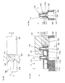
- FIG. 1( a ) is a plan view of a semiconductor device according to an embodiment of the present invention.
- FIG. 1( b ) is a cross-sectional view taken along line X-X′ in FIG. 1( a ) .
- FIG. 1( c ) is a cross-sectional view taken along line Y-Y′ in FIG. 1( a ) .
- FIG. 2( a ) is a plan view of a method for manufacturing a semiconductor device according to an embodiment of the present invention.
- FIG. 2( b ) is a cross-sectional view taken along line X-X′ in FIG. 2( a ) .
- FIG. 2( c ) is a cross-sectional view taken along line Y-Y′ in FIG. 2( a ) .
- FIG. 3( a ) is a plan view of a method for manufacturing a semiconductor device according to an embodiment of the present invention.
- FIG. 3( b ) is a cross-sectional view taken along line X-X′ in FIG. 3( a ) .
- FIG. 3( c ) is a cross-sectional view taken along line Y-Y′ in FIG. 3( a ) .
- FIG. 4( a ) is a plan view of a method for manufacturing a semiconductor device according to an embodiment of the present invention.
- FIG. 4( b ) is a cross-sectional view taken along line X-X′ in FIG. 4( a ) .
- FIG. 4( c ) is a cross-sectional view taken along line Y-Y′ in FIG. 4( a ) .
- FIG. 5( a ) is a plan view of a method for manufacturing a semiconductor device according to an embodiment of the present invention.
- FIG. 5( b ) is a cross-sectional view taken along line X-X′ in FIG. 5( a ) .
- FIG. 5( c ) is a cross-sectional view taken along line Y-Y′ in FIG. 5( a ) .
- FIG. 6( a ) is a plan view of a method for manufacturing a semiconductor device according to an embodiment of the present invention.
- FIG. 6( b ) is a cross-sectional view taken along line X-X′ in FIG. 6( a ) .
- FIG. 6( c ) is a cross-sectional view taken along line Y-Y′ in FIG. 6( a ) .
- FIG. 7( a ) is a plan view of a method for manufacturing a semiconductor device according to an embodiment of the present invention.
- FIG. 7( b ) is a cross-sectional view taken along line X-X′ in FIG. 7( a ) .
- FIG. 7( c ) is a cross-sectional view taken along line Y-Y′ in FIG. 7( a ) .
- FIG. 8( a ) is a plan view of a method for manufacturing a semiconductor device according to an embodiment of the present invention.
- FIG. 8( b ) is a cross-sectional view taken along line X-X′ in FIG. 8( a ) .
- FIG. 8( c ) is a cross-sectional view taken along line Y-Y′ in FIG. 8( a ) .
- FIG. 9( a ) is a plan view of a method for manufacturing a semiconductor device according to an embodiment of the present invention.
- FIG. 9( b ) is a cross-sectional view taken along line X-X′ in FIG. 9( a ) .
- FIG. 9( c ) is a cross-sectional view taken along line Y-Y′ in FIG. 9( a ) .
- FIG. 10( a ) is a plan view of a method for manufacturing a semiconductor device according to an embodiment of the present invention.
- FIG. 10( b ) is a cross-sectional view taken along line X-X′ in FIG. 10( a ) .
- FIG. 10( c ) is a cross-sectional view taken along line Y-Y′ in FIG. 10( a ) .
- FIG. 11( a ) is a plan view of a method for manufacturing a semiconductor device according to an embodiment of the present invention.
- FIG. 11( b ) is a cross-sectional view taken along line X-X′ in FIG. 11( a ) .
- FIG. 11( c ) is a cross-sectional view taken along line Y-Y′ in FIG. 11( a ) .
- FIG. 12( a ) is a plan view of a method for manufacturing a semiconductor device according to an embodiment of the present invention.
- FIG. 12( b ) is a cross-sectional view taken along line X-X′ in FIG. 12( a ) .
- FIG. 12( c ) is a cross-sectional view taken along line Y-Y′ in FIG. 12( a ) .
- FIG. 13( a ) is a plan view of a method for manufacturing a semiconductor device according to an embodiment of the present invention.
- FIG. 13( b ) is a cross-sectional view taken along line X-X′ in FIG. 13( a ) .
- FIG. 13( c ) is a cross-sectional view taken along line Y-Y′ in FIG. 13( a ) .
- FIG. 14( a ) is a plan view of a method for manufacturing a semiconductor device according to an embodiment of the present invention.
- FIG. 14( b ) is a cross-sectional view taken along line X-X′ in FIG. 14( a ) .
- FIG. 14( c ) is a cross-sectional view taken along line Y-Y′ in FIG. 14( a ) .
- FIG. 15( a ) is a plan view of a method for manufacturing a semiconductor device according to an embodiment of the present invention.
- FIG. 15 ( b ) is a cross-sectional view taken along line X-X′ in FIG. 15( a ) .
- FIG. 15( c ) is a cross-sectional view taken along line Y-Y′ in FIG. 15( a ) .
- FIG. 16( a ) is a plan view of a method for manufacturing a semiconductor device according to an embodiment of the present invention.
- FIG. 16( b ) is a cross-sectional view taken along line X-X′ in FIG. 16( a ) .
- FIG. 16( c ) is a cross-sectional view taken along line Y-Y′ in FIG. 16( a ) .
- FIG. 17( a ) is a plan view of a method for manufacturing a semiconductor device according to an embodiment of the present invention.
- FIG. 17( b ) is a cross-sectional view taken along line X-X′ in FIG. 17( a ) .
- FIG. 17( c ) is a cross-sectional view taken along line Y-Y′ in FIG. 17( a ) .
- FIG. 18( a ) is a plan view of a method for manufacturing a semiconductor device according to an embodiment of the present invention.
- FIG. 18( b ) is a cross-sectional view taken along line X-X′ in FIG. 18( a ) .
- FIG. 18( c ) is a cross-sectional view taken along line Y-Y′ in FIG. 18( a ) .
- FIG. 19( a ) is a plan view of a method for manufacturing a semiconductor device according to an embodiment of the present invention.
- FIG. 19( b ) is a cross-sectional view taken along line X-X′ in FIG. 19( a ) .
- FIG. 19( c ) is a cross-sectional view taken along line Y-Y′ in FIG. 19( a ) .
- FIG. 20( a ) is a plan view of a method for manufacturing a semiconductor device according to an embodiment of the present invention.
- FIG. 20( b ) is a cross-sectional view taken along line X-X′ in FIG. 20( a ) .
- FIG. 20( c ) is a cross-sectional view taken along line Y-Y′ in FIG. 20( a ) .
- FIG. 21( a ) is a plan view of a method for manufacturing a semiconductor device according to an embodiment of the present invention.
- FIG. 21( b ) is a cross-sectional view taken along line X-X′ in FIG. 21( a ) .
- FIG. 21( c ) is a cross-sectional view taken along line Y-Y′ in FIG. 21( a ) .
- FIG. 22( a ) is a plan view of a method for manufacturing a semiconductor device according to an embodiment of the present invention.
- FIG. 22( b ) is a cross-sectional view taken along line X-X′ in FIG. 22( a ) .
- FIG. 22( c ) is a cross-sectional view taken along line Y-Y′ in FIG. 22( a ) .
- FIG. 23( a ) is a plan view of a method for manufacturing a semiconductor device according to an embodiment of the present invention.
- FIG. 23 ( b ) is a cross-sectional view taken along line X-X′ in FIG. 23( a ) .
- FIG. 23( c ) is a cross-sectional view taken along line Y-Y′ in FIG. 23( a ) .
- FIG. 24( a ) is a plan view of a method for manufacturing a semiconductor device according to an embodiment of the present invention.
- FIG. 24( b ) is a cross-sectional view taken along line X-X′ in FIG. 24( a ) .
- FIG. 24( c ) is a cross-sectional view taken along line Y-Y′ in FIG. 24( a ) .
- FIG. 25( a ) is a plan view of a method for manufacturing a semiconductor device according to an embodiment of the present invention.
- FIG. 25( b ) is a cross-sectional view taken along line X-X′ in FIG. 25( a ) .
- FIG. 25( c ) is a cross-sectional view taken along line Y-Y′ in FIG. 25( a ) .
- FIG. 26( a ) is a plan view of a method for manufacturing a semiconductor device according to an embodiment of the present invention.
- FIG. 26( b ) is a cross-sectional view taken along line X-X′ in FIG. 26( a ) .
- FIG. 26( c ) is a cross-sectional view taken along line Y-Y′ in FIG. 26( a ) .
- FIG. 27( a ) is a plan view of a method for manufacturing a semiconductor device according to an embodiment of the present invention.
- FIG. 27( b ) is a cross-sectional view taken along line X-X′ in FIG. 27( a ) .
- FIG. 27( c ) is a cross-sectional view taken along line Y-Y′ in FIG. 27( a ) .
- FIG. 28( a ) is a plan view of a method for manufacturing a semiconductor device according to an embodiment of the present invention.
- FIG. 28( b ) is a cross-sectional view taken along line X-X′ in FIG. 28( a ) .
- FIG. 28( c ) is a cross-sectional view taken along line Y-Y′ in FIG. 28( a ) .
- FIG. 29( a ) is a plan view of a method for manufacturing a semiconductor device according to an embodiment of the present invention.
- FIG. 29( b ) is a cross-sectional view taken along line X-X′ in FIG. 29( a ) .
- FIG. 29( c ) is a cross-sectional view taken along line Y-Y′ in FIG. 29( a ) .
- FIG. 30( a ) is a plan view of a method for manufacturing a semiconductor device according to an embodiment of the present invention.
- FIG. 30( b ) is a cross-sectional view taken along line X-X′ in FIG. 30( a ) .
- FIG. 30( c ) is a cross-sectional view taken along line Y-Y′ in FIG. 30( a ) .
- FIG. 31( a ) is a plan view of a method for manufacturing a semiconductor device according to an embodiment of the present invention.
- FIG. 31 ( b ) is a cross-sectional view taken along line X-X′ in FIG. 31( a ) .
- FIG. 31( c ) is a cross-sectional view taken along line Y-Y′ in FIG. 31( a ) .
- FIG. 32( a ) is a plan view of a method for manufacturing a semiconductor device according to an embodiment of the present invention.
- FIG. 32( b ) is a cross-sectional view taken along line X-X′ in FIG. 32( a ) .
- FIG. 32( c ) is a cross-sectional view taken along line Y-Y′ in FIG. 32( a ) .
- FIG. 33( a ) is a plan view of a method for manufacturing a semiconductor device according to an embodiment of the present invention.
- FIG. 33( b ) is a cross-sectional view taken along line X-X′ in FIG. 33( a ) .
- FIG. 33( c ) is a cross-sectional view taken along line Y-Y′ in FIG. 33( a ) .
- FIG. 34( a ) is a plan view of a method for manufacturing a semiconductor device according to an embodiment of the present invention.
- FIG. 34( b ) is a cross-sectional view taken along line X-X′ in FIG. 34( a ) .
- FIG. 34( c ) is a cross-sectional view taken along line Y-Y′ in FIG. 34( a ) .
- FIG. 35( a ) is a plan view of a method for manufacturing a semiconductor device according to an embodiment of the present invention.
- FIG. 35( b ) is a cross-sectional view taken along line X-X′ in FIG. 35( a ) .
- FIG. 35( c ) is a cross-sectional view taken along line Y-Y′ in FIG. 35( a ) .
- FIG. 36( a ) is a plan view of a method for manufacturing a semiconductor device according to an embodiment of the present invention.
- FIG. 36( b ) is a cross-sectional view taken along line X-X′ in FIG. 36( a ) .
- FIG. 36( c ) is a cross-sectional view taken along line Y-Y′ in FIG. 36( a ) .
- FIG. 37( a ) is a plan view of a method for manufacturing a semiconductor device according to an embodiment of the present invention.
- FIG. 37( b ) is a cross-sectional view taken along line X-X′ in FIG. 37( a ) .
- FIG. 37( c ) is a cross-sectional view taken along line Y-Y′ in FIG. 37( a ) .
- FIG. 38( a ) is a plan view of a method for manufacturing a semiconductor device according to an embodiment of the present invention.
- FIG. 38( b ) is a cross-sectional view taken along line X-X′ in FIG. 38( a ) .
- FIG. 38( c ) is a cross-sectional view taken along line Y-Y′ in FIG. 38( a ) .
- FIG. 39( a ) is a plan view of a method for manufacturing a semiconductor device according to an embodiment of the present invention.
- FIG. 39 ( b ) is a cross-sectional view taken along line X-X′ in FIG. 39( a ) .
- FIG. 39( c ) is a cross-sectional view taken along line Y-Y′ in FIG. 39( a ) .
- FIG. 40( a ) is a plan view of a method for manufacturing a semiconductor device according to an embodiment of the present invention.
- FIG. 40( b ) is a cross-sectional view taken along line X-X′ in FIG. 40( a ) .
- FIG. 40( c ) is a cross-sectional view taken along line Y-Y′ in FIG. 40( a ) .
- FIG. 41( a ) is a plan view of a method for manufacturing a semiconductor device according to an embodiment of the present invention.
- FIG. 41( b ) is a cross-sectional view taken along line X-X′ in FIG. 41( a ) .
- FIG. 41( c ) is a cross-sectional view taken along line Y-Y′ in FIG. 41( a ) .
- FIG. 42( a ) is a plan view of a method for manufacturing a semiconductor device according to an embodiment of the present invention.
- FIG. 42( b ) is a cross-sectional view taken along line X-X′ in FIG. 42( a ) .
- FIG. 42( c ) is a cross-sectional view taken along line Y-Y′ in FIG. 42( a ) .
- FIG. 43( a ) is a plan view of a method for manufacturing a semiconductor device according to an embodiment of the present invention.
- FIG. 43( b ) is a cross-sectional view taken along line X-X′ in FIG. 43( a ) .
- FIG. 43( c ) is a cross-sectional view taken along line Y-Y′ in FIG. 43( a ) .
- a semiconductor device having a SGT structure according to an embodiment of the present invention is described below with reference to FIG. 1 .
- planar silicon layer 107 formed on a silicon substrate 101 ;
- a gate line 117 c connected to the first gate electrode 117 b;
- a second n-type diffusion layer 120 formed in a lower portion of the first pillar-shaped silicon layer 105 and in an upper portion of the planar silicon layer 107 ;
- a first sidewall 201 having a laminated structure of an insulating film 127 and polysilicon 115 and being formed on an upper sidewall of the first pillar-shaped silicon layer 105 and an upper portion of the first gate electrode 117 b ;
- first contact 146 is connected to the polysilicon 115 of the first sidewall 201 ;
- the conductivity type of the polysilicon 115 of the first sidewall 201 is n-type.
- the semiconductor device further includes first silicides 135 and 134 formed on the first n-type diffusion layer 119 and the first sidewall 201 .
- a silicide satisfactorily stops contact etching because of a high selection ratio for etching an oxide film.
- the polysilicon 115 of the first sidewall 201 which has a laminated structure including the insulating film 127 and the polysilicon 115 and which is formed on an upper sidewall of the first pillar-shaped silicon layer 105 and an upper portion of the first gate electrode 117 b . Since the insulating film 127 of the first sidewall 201 is thin and held in the polysilicon 115 , the etching rate is decreased to stop contact etching by the first sidewall 201 . Therefore, the height from the upper surface of the first n-type diffusion layer to the upper surface of the first gate electrode 117 b can be reduced.
- the conductivity type of the polysilicon of the first sidewall 201 is n-type, surface carriers are induced by a difference in work function, and thus the resistance in an upper portion of a pillar-shaped silicon layer 105 can be decreased.
- the conductivity type of the polysilicon of the first sidewall 201 is n+-type, and the pillar-shaped silicon layer 105 has a low impurity concentration, a transistor composed of the first sidewall 201 and the pillar-shaped silicon layer 105 is turned on when a voltage applied to the first sidewall 201 through the contact 146 is 0 V.
- a channel of the transistor can be electrically connected to the first n-type diffusion layer 119 .
- the polysilicon of the first sidewall 201 is formed on an upper sidewall of the pillar-shaped silicon layer 105 , and thus the first sidewall 201 has a larger diameter than that of the pillar-shaped silicon layer 105 .
- the pillar-shaped silicon layer 105 becomes thin and thus has difficulty in implanting an impurity in the pillar-shaped silicon layer 105 , an impurity can be implanted into the polysilicon 115 of the first sidewall 201 . Therefore, a channel of the transistor can be electrically connected to the first n-type diffusion layer.
- the first gate electrode 117 b has a laminated structure of a metal 110 and polysilicon 111 .
- SGT has the first sidewall 201 having a laminated structure of the insulating film 127 and the polysilicon 115 and formed on an upper sidewall of the first pillar-shaped silicon layer 105 and an upper portion of the first gate electrode 117 b.
- CMOS SGT using the SGT according to the embodiment of the present invention is described below.
- the CMOS SGT includes:
- a first p-type diffusion layer 122 formed in an upper portion of the second pillar-shaped silicon layer 104 ;
- a second p-type diffusion layer 123 formed in a lower portion of the second pillar-shaped silicon layer 104 and an upper portion of the planar silicon layer 107 ;
- a second sidewall 202 having a laminated structure of an insulating film 126 and polysilicon 114 and being formed on an upper sidewall of the second pillar-shaped silicon layer 104 and on an upper portion of the second gate electrode 117 a ;
- the conductivity type of the polysilicon 114 of the second sidewall 202 is p-type.
- the CMOS SGT further includes second silicides 129 and 130 formed on the first p-type diffusion layer 122 and the first sidewall 202 .
- the lower surface of the first p-type diffusion layer 122 is higher than the upper surface of the second gate electrode 117 a.
- the second gate electrode 117 a has a laminated structure of a metal 110 and polysilicon 111 .
- the second n-type diffusion layer 120 and the second p-type diffusion layer 123 are connected to each other through a silicide.
- CMOS SGT using the SGT according to the present invention is described above.
- a process for manufacturing a semiconductor device having a SGT structure according to an embodiment of the present invention is described below with reference to FIGS. 2 to 43 .
- first resists 102 and 103 are formed for forming the first pillar-shaped silicon layer 105 and the second pillar-shaped silicon layer 104 on the silicon substrate 101 .
- the silicon substrate 101 is etched to form the first pillar-shaped silicon layer 105 and the second pillar-shaped silicon layer 104 .
- a second resist 106 is formed for forming the planar silicon layer 107 .
- the silicon substrate 101 is etched to form the planar silicon layer 107 .
- an oxide film 108 is deposited and the surface thereof is planarized.
- the oxide film 108 is etched to be left around the planar silicon layer 107 .
- the gate insulating film 109 is formed around the first pillar-shaped silicon layer 105 and the second pillar-shaped silicon layer 104 .
- an oxide film, a laminated structure of an oxide film and a nitride film, a nitride film, or a high-dielectric film can be used as a material of the gate insulating film 109 .
- the metal film 110 is formed around the gate insulating film 109 .
- a metal material which can be used for a gate electrode such as titanium, titanium nitride, tantalum, tantalum nitride, or the like, can be used for the metal film 110 .
- polysilicon 111 is deposited and the surface thereof is planarized.
- the polysilicon 111 is etched.
- the polysilicon 111 is etched to expose upper portions of the first pillar-shaped silicon layer 105 and the second pillar-shaped silicon layer 104 .
- the metal film 110 is etched.
- wet etching is preferably used.
- a thin insulating film 112 and polysilicon 113 are deposited.
- the polysilicon 113 is etched to leave the polysilicon 114 and 115 as sidewalls on an upper sidewall of the first pillar-shaped silicon layer 105 and an upper sidewall of the second pillar-shaped silicon layer 104 .
- a third resist 116 is formed for forming the first gate electrode 117 b , the second gate electrode 117 a , and the gate line 117 c.
- the insulating film 112 is etched.
- the polysilicon 111 , the metal film 110 , and the gate insulating film 109 are etched to form the first gate electrode 117 b , the second gate electrode 117 a , and the gate line 117 c.
- a fourth resist 118 is formed for forming the first n-type diffusion layer 119 and the second n-type diffusion layer 120 .
- arsenic is implanted to form the first n-type diffusion layer 119 and the second n-type diffusion layer 120 .
- arsenic is also implanted into the polysilicon 115 of the sidewall.
- arsenic is implanted into the polysilicon 115 from the sidewall thereof, thereby easily achieving n-type at a high concentration.
- a fifth resist 121 is formed for forming the first p-type diffusion layer 122 and the second p-type diffusion layer 123 .
- boron is implanted to form the first p-type diffusion layer 122 and the second p-type diffusion layer 123 .
- boron is also implanted into the polysilicon 114 of the sidewall.
- boron is implanted into the polysilicon 114 from the sidewall thereof, thereby easily achieving p-type at a high-concentration.
- the nitride film 124 is deposited.
- heat treatment is performed.
- a shallow junction can be formed by decreasing heat treatment.
- heat treatment is performed to form a deep junction, the second n-type diffusion layer 120 and the second p-type diffusion layer 123 are widened in the lateral direction, thereby causing difficulty in increasing integration.
- the nitride film 124 is etched, and the insulating film 112 is etched to form the nitride film sidewall 125 .
- the first sidewall 201 including the insulating film 127 and the polysilicon 115 is formed on an upper sidewall of the first pillar-shaped silicon layer 105
- the second sidewall 202 including the insulating film 126 and the polysilicon 114 is formed on an upper sidewall of the second pillar-shaped silicon layer 104 .
- silicide 135 , silicide 134 , silicide 129 , and silicide 130 are formed on the first n-type diffusion layer 119 , the polysilicon 115 , the first p-type diffusion layer 122 , and the polysilicon 114 , respectively.
- silicides 128 , 131 , 132 , 133 , and 136 are formed.
- an interlayer insulating film 137 is deposited and planarized.
- a sixth resist 138 is formed for forming the first contact 146 and the second contact 145 .
- the interlayer insulating film 137 is etched to form contact holes 139 and 140 .
- contact etching is stopped at the polysilicon by the first sidewall having a laminated structure of the insulating film and the polysilicon and being formed on an upper sidewall of the first pillar-shaped silicon layer and an upper portion of the first gate electrode. Since the insulating film of the first sidewall is thin and held in the polysilicon, the etching rate is decreased to stop contact etching by the first sidewall.
- a seventh resist 141 is formed for forming the contacts 144 and 147 .
- the interlayer insulating film 137 is etched to form contact holes 142 and 143 .
- a metal is deposited to form the contacts 144 and 147 , the first contact 146 , and the second contact 145 .
- a metal 148 is deposited.
- eighth resists 149 , 150 , 151 , and 152 are formed for forming metal lines 153 , 154 , 155 , and 156 .
- the metal 148 is etched to form the metal lines 153 , 154 , 155 , and 156 .
- the eighth resists 149 , 150 , 151 , and 152 are removed.
Abstract
A semiconductor device includes a pillar-shaped semiconductor layer and a sidewall having a laminated structure. The laminated structure includes an insulating film and silicon, and the laminated structure is on an upper sidewall of the first pillar-shaped semiconductor layer. The silicon is electrically connected to a top of the pillar-shaped semiconductor layer.
Description
This application is a continuation of U.S. application Ser. No. 14/645,727, filed Mar. 12, 2015, now U.S. Pat. No. 9,153,660, which is a continuation of U.S. application Ser. No. 14/100,456, filed Dec. 9, 2013, now U.S. Pat. No. 9,012,981, which is a continuation-in-part of U.S. application Ser. No. 13/891,584, filed May 10, 2013, now U.S. Pat. No. 8,829,601, which claims the benefit of the filing date of U.S. Provisional Patent Appl. Ser. No. 61/648,183 filed May 17, 2012. The entire contents of which are hereby incorporated by reference.
1. Technical Field
The present invention relates to a semiconductor device.
2. Description of the Related Art
Semiconductor integrated circuits, particularly integrated circuits using MOS transistors, are increasing in integration. With increases in integration, MOS transistors used in the integrated circuits increasingly become finer up to a nano-level. Such finer MOS transistors have difficulty in suppressing leak currents and difficulty in decreasing areas occupied by circuits in view of the demand for securing necessary amounts of currents. In order to resolve the problem, there are proposed surrounding gate transistors (referred to as “SGT” hereinafter) having a structure in which a source, gate, and drain are disposed perpendicularly to a substrate, and a gate electrode surrounds a pillar-shaped semiconductor layer (for example, refer to Japanese Unexamined Patent Application Publication Nos. 2-715562, 2-188966, and 3-145761).
A conventional SGT manufacturing method includes forming a silicon pillar having a pillar-shaped nitride film hard mask formed thereon, forming a diffusion layer in a lower portion of the silicon pillar, depositing a gate material, planarizing the gate material, etching back the gate material, and forming an insulating film sidewall on sidewalls of the silicon pillar and the nitride film hard mask. Then, a resist pattern for a gate line is formed, the gate material is etched, the nitride film hard mask is removed, and a diffusion layer is formed in an upper portion of the silicon pillar (for example, refer to Japanese Unexamined Patent Application Publication No. 2009-182317). Then, a nitride film sidewall is formed on the sidewall of the silicon pillar, a diffusion layer is formed in an upper portion of the silicon pillar by ion implantation, a nitride film is formed as a contact stopper, an oxide film is formed as an interlayer film, and then contact etching is performed.
It is known that oxide film etching for forming a contact has a high selection ratio to a nitride film in a flat portion, but the selection ratio in a nitride film shoulder portion is lower than that in the flat portion.
Since the diameter of a silicon pillar of SGT decreases with reduction in size, a flat area is decreased. In addition, a nitride film sidewall corresponds to a nitride film shoulder portion, and thus the selection ratio of etching an oxide film is decreased. Therefore, etching an oxide film to form a contact on a silicon pillar is not stopped by a nitride film to form a contact hole which reaches a gate, resulting in short-circuiting between the silicon pillar and the gate.
There is proposed a structure for preventing the occurrence of short-circuiting between a contact and a gate by forming an epitaxial semiconductor layer on a silicon pillar of SGT (refer to, for example, Japanese Unexamined Patent Application Publication No. 2010-258345). However, epitaxial growth requires insulating film sidewalls to be formed on an upper sidewall of the silicon pillar and on an upper portion of a gate electrode. When polysilicon is used in a gate, silicon is also grown on the gate. Therefore, epitaxial growth to a height equal to or higher than the height of the insulating film sidewall causes short-circuiting between the gate and an upper portion of the silicon pillar.
On the other hand, the nitride film sidewall is formed on the sidewall of the silicon pillar, and the diffusion layer is formed in an upper portion of the silicon pillar by ion implantation. Therefore, ions are implanted from above into an upper portion of the silicon pillar, and thus a deep diffusion layer is required to be formed. When a deep diffusion layer is formed, the diffusion layer is also widened in the lateral direction. That is, higher integration becomes difficult to achieve.
In addition, when the silicon pillar becomes thin, it is difficult to allow impurities to present in the silicon pillar because the silicon density is 5×10²²/cm3.
It is described that in a flat-type MOS transistor, a sidewall of a LDD region is composed of polycrystal silicon having the same conductivity type as a low-concentration layer, and surface carriers of the LDD region are induced by a difference in work function, thereby decreasing the impedance of the LDD region as compared an oxide film sidewall LDD-type MOS transistor (refer to, for example, Japanese Unexamined Patent Application Publication No. 11-297984). It is also described that the polycrystal silicon sidewall is electrically insulated from the gate electrode. Also, drawings show that the polycrystal silicon sidewall is insulated from source/drain through an interlayer insulating film.
Accordingly, an object of the present invention is to provide a SGT structure having a structure for decreasing the resistance of an upper portion of a silicon pillar and a method for manufacturing the SGT.
A semiconductor device according to a first embodiment of the present invention includes: a pillar-shaped semiconductor layer and a sidewall having a laminated structure. The laminated structure includes an insulating film and silicon, and the laminated structure is on an upper sidewall of the first pillar-shaped semiconductor layer. The silicon is electrically connected to a top of the pillar-shaped semiconductor layer.
The semiconductor device preferably includes a first silicide formed on the first first-conductivity-type diffusion layer and on the first sidewall.
The lower surface of the first first-conductivity-type diffusion layer is preferably higher than the upper surface of the first gate electrode.
The first gate electrode preferably has a laminated structure of a metal and polysilicon.
A semiconductor device according to a second embodiment of the present invention further includes, in the semiconductor device according to the first embodiment:
the planar semiconductor layer formed on the semiconductor substrate;
a second pillar-shaped semiconductor layer formed on the planar semiconductor layer;
the gate insulating film formed around the second pillar-shaped semiconductor layer;
a second gate electrode formed around the gate insulating film;
the gate line connected to the second gate electrode;
a first second-conductivity-type diffusion layer formed in an upper portion of the second pillar-shaped semiconductor layer;
a second second-conductivity-type diffusion layer formed in a lower portion of the second pillar-shaped semiconductor layer and in an upper portion of the planar semiconductor layer;
a second sidewall having a laminated structure of an insulating film and polysilicon and being formed on an upper sidewall of the second pillar-shaped semiconductor layer and on an upper portion of the second gate electrode; and
a second contact formed on the first second-conductivity-type diffusion layer and on the second sidewall,
wherein the second contact is connected to the polysilicon of the second sidewall; and
the conductivity type of the polysilicon of the second sidewall is the second conductivity type.
The semiconductor device preferably includes a first silicide formed on the first first-conductivity-type diffusion layer and on the first sidewall, and a second silicide formed on the first second-conductivity-type diffusion layer and on the second sidewall.
The lower surface of the first first-conductivity-type diffusion layer is preferably higher than the upper surface of the first gate electrode, and the lower surface of the first second-conductivity-type diffusion layer is preferably higher than the upper surface of the second gate electrode.
The first gate electrode preferably has a laminated structure of a metal and polysilicon, and the second gate electrode preferably has a laminated structure of a metal and polysilicon.
The first sidewall can be formed by depositing the insulating film and the polysilicon on the first pillar-shaped semiconductor layer and etching the polysilicon to leave it as a sidewall.
According to the present invention, contact etching is stopped by the polysilicon of the first sidewall having a laminated structure including the insulating film and the polysilicon and formed on an upper sidewall of the first pillar-shaped silicon layer and an upper portion of the first gate electrode. Since the insulating film of the first sidewall is thin and held in the polysilicon, the etching rate is decreased to stop contact etching by the first sidewall. Therefore, the height from the upper surface of the first first-conductivity-type diffusion layer to the upper surface of the first gate electrode can be decreased.
Also since the conductivity type of the polysilicon of the first sidewall is the first conductivity type, surface carriers are induced by a difference in work function, and thus the resistance in an upper portion of a pillar-shaped silicon layer can be decreased. For example, when the first sidewall is n+ type, and the pillar-shaped silicon layer has a low impurity concentration, a transistor composed of the first sidewall and the pillar-shaped silicon layer is turned on when a voltage applied to the first sidewall through the contact is 0 V.
As described above, when the lower surface of the first first-conductivity-type diffusion layer is higher than the upper surface of the first gate electrode, a channel of the transistor can be electrically connected to the first first-conductivity-type diffusion layer.
When an impurity is introduced so that the lower surface of the first first-conductivity-type diffusion layer is higher than the upper surface of the first gate electrode, a shallow junction is formed, thereby reducing the widening of the diffusion layer in the lateral direction. That is, higher integration can be realized.
The polysilicon of the first sidewall is formed on an upper sidewall of the pillar-shaped silicon layer, and thus the first sidewall has a larger diameter than that of the pillar-shaped silicon layer. Although the pillar-shaped silicon layer becomes thin and thus has difficulty in implanting impurities in the pillar-shaped silicon layer, impurities can be implanted into the polysilicon of the first sidewall. Therefore, a channel of the transistor can be electrically connected to the first first-conductivity-type diffusion layer.
A semiconductor device having a SGT structure according to an embodiment of the present invention is described below with reference to FIG. 1 .
A semiconductor device having a SGT structure according to an embodiment of the present invention includes:
a planar silicon layer 107 formed on a silicon substrate 101;
a first pillar-shaped silicon layer 105 formed on the planar silicon layer 107;
a gate insulating film 109 formed around the first pillar-shaped silicon layer 105;
a first gate electrode 117 b formed around the gate insulating film 109;
a gate line 117 c connected to the first gate electrode 117 b;
a first n-type diffusion layer 119 formed in an upper portion of the first pillar-shaped silicon layer 105;
a second n-type diffusion layer 120 formed in a lower portion of the first pillar-shaped silicon layer 105 and in an upper portion of the planar silicon layer 107;
a first sidewall 201 having a laminated structure of an insulating film 127 and polysilicon 115 and being formed on an upper sidewall of the first pillar-shaped silicon layer 105 and an upper portion of the first gate electrode 117 b; and
a first contact 146 formed on the first n-type diffusion layer 119 and the first sidewall 201,
wherein the first contact 146 is connected to the polysilicon 115 of the first sidewall 201; and
the conductivity type of the polysilicon 115 of the first sidewall 201 is n-type.
The semiconductor device further includes first silicides 135 and 134 formed on the first n-type diffusion layer 119 and the first sidewall 201. A silicide satisfactorily stops contact etching because of a high selection ratio for etching an oxide film.
Contact etching is stopped by the polysilicon 115 of the first sidewall 201 which has a laminated structure including the insulating film 127 and the polysilicon 115 and which is formed on an upper sidewall of the first pillar-shaped silicon layer 105 and an upper portion of the first gate electrode 117 b. Since the insulating film 127 of the first sidewall 201 is thin and held in the polysilicon 115, the etching rate is decreased to stop contact etching by the first sidewall 201. Therefore, the height from the upper surface of the first n-type diffusion layer to the upper surface of the first gate electrode 117 b can be reduced.
Also since the conductivity type of the polysilicon of the first sidewall 201 is n-type, surface carriers are induced by a difference in work function, and thus the resistance in an upper portion of a pillar-shaped silicon layer 105 can be decreased. For example, when the first sidewall 201 is n+-type, and the pillar-shaped silicon layer 105 has a low impurity concentration, a transistor composed of the first sidewall 201 and the pillar-shaped silicon layer 105 is turned on when a voltage applied to the first sidewall 201 through the contact 146 is 0 V.
As described above, when the lower surface of the first n-type diffusion layer 119 is higher than the upper surface of the first gate electrode 117 b, a channel of the transistor can be electrically connected to the first n-type diffusion layer 119.
When impurities are introduced so that the lower surface of the first n-type diffusion layer 119 is higher than the upper surface of the first gate electrode 117 b, a shallow junction is formed, thereby reducing the widening of the diffusion layer in the lateral direction. That is, higher integration can be realized.
The polysilicon of the first sidewall 201 is formed on an upper sidewall of the pillar-shaped silicon layer 105, and thus the first sidewall 201 has a larger diameter than that of the pillar-shaped silicon layer 105. Although the pillar-shaped silicon layer 105 becomes thin and thus has difficulty in implanting an impurity in the pillar-shaped silicon layer 105, an impurity can be implanted into the polysilicon 115 of the first sidewall 201. Therefore, a channel of the transistor can be electrically connected to the first n-type diffusion layer.
The first gate electrode 117 b has a laminated structure of a metal 110 and polysilicon 111.
Consequently, SGT has the first sidewall 201 having a laminated structure of the insulating film 127 and the polysilicon 115 and formed on an upper sidewall of the first pillar-shaped silicon layer 105 and an upper portion of the first gate electrode 117 b.
CMOS SGT using the SGT according to the embodiment of the present invention is described below. The CMOS SGT includes:
a second pillar-shaped silicon layer 104 formed on the planar silicon layer 107;
the gate insulating film 109 formed around the second pillar-shaped silicon layer 104;
a second gate electrode 117 a formed around the gate insulating film 109;
the gate line 117 c connected to the second gate electrode 117 a;
a first p-type diffusion layer 122 formed in an upper portion of the second pillar-shaped silicon layer 104;
a second p-type diffusion layer 123 formed in a lower portion of the second pillar-shaped silicon layer 104 and an upper portion of the planar silicon layer 107;
a second sidewall 202 having a laminated structure of an insulating film 126 and polysilicon 114 and being formed on an upper sidewall of the second pillar-shaped silicon layer 104 and on an upper portion of the second gate electrode 117 a; and
a second contact 145 formed on the first p-type diffusion layer 122 and on the second sidewall 202,
wherein the second contact 145 is connected to the polysilicon 114 of the second sidewall 202; and
the conductivity type of the polysilicon 114 of the second sidewall 202 is p-type.
The CMOS SGT further includes second silicides 129 and 130 formed on the first p-type diffusion layer 122 and the first sidewall 202.
The lower surface of the first p-type diffusion layer 122 is higher than the upper surface of the second gate electrode 117 a.
The second gate electrode 117 a has a laminated structure of a metal 110 and polysilicon 111.
The second n-type diffusion layer 120 and the second p-type diffusion layer 123 are connected to each other through a silicide.
The CMOS SGT using the SGT according to the present invention is described above.
A process for manufacturing a semiconductor device having a SGT structure according to an embodiment of the present invention is described below with reference to FIGS. 2 to 43 .
First, as shown in FIG. 2 , first resists 102 and 103 are formed for forming the first pillar-shaped silicon layer 105 and the second pillar-shaped silicon layer 104 on the silicon substrate 101.
Next, as shown in FIG. 3 , the silicon substrate 101 is etched to form the first pillar-shaped silicon layer 105 and the second pillar-shaped silicon layer 104.
Then, as shown in FIG. 4 , the first resists 102 and 103 are removed.
Then, as shown in FIG. 5 , a second resist 106 is formed for forming the planar silicon layer 107.
Then, as shown in FIG. 6 , the silicon substrate 101 is etched to form the planar silicon layer 107.
Then, as shown in FIG. 7 , the second resist 106 is removed.
Next, as shown in FIG. 8 , an oxide film 108 is deposited and the surface thereof is planarized.
Then, as shown in FIG. 9 , the oxide film 108 is etched to be left around the planar silicon layer 107.
First, as shown in FIG. 10 , the gate insulating film 109 is formed around the first pillar-shaped silicon layer 105 and the second pillar-shaped silicon layer 104. In this case, an oxide film, a laminated structure of an oxide film and a nitride film, a nitride film, or a high-dielectric film can be used as a material of the gate insulating film 109.
Next, as shown in FIG. 11 , the metal film 110 is formed around the gate insulating film 109. A metal material which can be used for a gate electrode, such as titanium, titanium nitride, tantalum, tantalum nitride, or the like, can be used for the metal film 110.
Then, as shown in FIG. 12 , polysilicon 111 is deposited and the surface thereof is planarized.
Then, as shown in FIG. 13 , the polysilicon 111 is etched.
Then, as shown in FIG. 14 , the polysilicon 111 is etched to expose upper portions of the first pillar-shaped silicon layer 105 and the second pillar-shaped silicon layer 104.
Then, as shown in FIG. 15 , the metal film 110 is etched. In this case, wet etching is preferably used.
Then, as shown in FIG. 16 , a thin insulating film 112 and polysilicon 113 are deposited.
Then, as shown in FIG. 17 , the polysilicon 113 is etched to leave the polysilicon 114 and 115 as sidewalls on an upper sidewall of the first pillar-shaped silicon layer 105 and an upper sidewall of the second pillar-shaped silicon layer 104.
Then, as shown in FIG. 18 , a third resist 116 is formed for forming the first gate electrode 117 b, the second gate electrode 117 a, and the gate line 117 c.
Then, as shown in FIG. 19 , the insulating film 112 is etched.
Then, as shown in FIG. 20 , the polysilicon 111, the metal film 110, and the gate insulating film 109 are etched to form the first gate electrode 117 b, the second gate electrode 117 a, and the gate line 117 c.
Then, as shown in FIG. 21 , the third resist 116 is removed.
Then, as shown in FIG. 22 , a fourth resist 118 is formed for forming the first n-type diffusion layer 119 and the second n-type diffusion layer 120.
Then, as shown in FIG. 23 , arsenic is implanted to form the first n-type diffusion layer 119 and the second n-type diffusion layer 120. At this time, arsenic is also implanted into the polysilicon 115 of the sidewall. Also, arsenic is implanted into the polysilicon 115 from the sidewall thereof, thereby easily achieving n-type at a high concentration.
Then, as shown in FIG. 24 , the fourth resist 118 is removed.
Then, as shown in FIG. 25 , a fifth resist 121 is formed for forming the first p-type diffusion layer 122 and the second p-type diffusion layer 123.
Then, as shown in FIG. 26 , boron is implanted to form the first p-type diffusion layer 122 and the second p-type diffusion layer 123. At this time, boron is also implanted into the polysilicon 114 of the sidewall. Also, boron is implanted into the polysilicon 114 from the sidewall thereof, thereby easily achieving p-type at a high-concentration.
Then, as shown in FIG. 27 , the fifth resist 121 is removed.
Then, as shown in FIG. 28 , the nitride film 124 is deposited.
Then, as shown in FIG. 29 , heat treatment is performed. In this treatment, a shallow junction can be formed by decreasing heat treatment. When heat treatment is performed to form a deep junction, the second n-type diffusion layer 120 and the second p-type diffusion layer 123 are widened in the lateral direction, thereby causing difficulty in increasing integration.
Then, as shown in FIG. 30 , the nitride film 124 is etched, and the insulating film 112 is etched to form the nitride film sidewall 125. At the same time, the first sidewall 201 including the insulating film 127 and the polysilicon 115 is formed on an upper sidewall of the first pillar-shaped silicon layer 105, and the second sidewall 202 including the insulating film 126 and the polysilicon 114 is formed on an upper sidewall of the second pillar-shaped silicon layer 104.
Then, as shown in FIG. 31 , silicide 135, silicide 134, silicide 129, and silicide 130 are formed on the first n-type diffusion layer 119, the polysilicon 115, the first p-type diffusion layer 122, and the polysilicon 114, respectively. In addition, silicides 128, 131, 132, 133, and 136 are formed.
Then, as shown in FIG. 32 , an interlayer insulating film 137 is deposited and planarized.
Then, as shown in FIG. 33 , a sixth resist 138 is formed for forming the first contact 146 and the second contact 145.
Then, as shown in FIG. 34 , the interlayer insulating film 137 is etched to form contact holes 139 and 140. In this case, contact etching is stopped at the polysilicon by the first sidewall having a laminated structure of the insulating film and the polysilicon and being formed on an upper sidewall of the first pillar-shaped silicon layer and an upper portion of the first gate electrode. Since the insulating film of the first sidewall is thin and held in the polysilicon, the etching rate is decreased to stop contact etching by the first sidewall.
Then, as shown in FIG. 35 , the sixth resist 138 is removed.
Then, as shown in FIG. 36 , a seventh resist 141 is formed for forming the contacts 144 and 147.
Then, as shown in FIG. 37 , the interlayer insulating film 137 is etched to form contact holes 142 and 143.
Then, as shown in FIG. 38 , the seventh resist 137 is removed.
Then, as shown in FIG. 39 , a metal is deposited to form the contacts 144 and 147, the first contact 146, and the second contact 145.
Then, as shown in FIG. 40 , a metal 148 is deposited.
Then, as shown in FIG. 41 , eighth resists 149, 150, 151, and 152 are formed for forming metal lines 153, 154, 155, and 156.
Then, as shown in FIG. 42 , the metal 148 is etched to form the metal lines 153, 154, 155, and 156.
Then, as shown in FIG. 43 , the eighth resists 149, 150, 151, and 152 are removed.
Claims (1)
1. A semiconductor device comprising:
a pillar-shaped semiconductor layer; and
a sidewall having a laminated structure comprising an insulating film and silicon, the sidewall on an upper sidewall of the pillar-shaped semiconductor layer,
wherein the silicon of the sidewall is electrically connected to a top of the pillar-shaped semiconductor layer.
Priority Applications (1)
| Application Number | Priority Date | Filing Date | Title |
|---|---|---|---|
| US14/824,512 US9299786B2 (en) | 2012-05-17 | 2015-08-12 | Semiconductor device |
Applications Claiming Priority (5)
| Application Number | Priority Date | Filing Date | Title |
|---|---|---|---|
| US201261648183P | 2012-05-17 | 2012-05-17 | |
| US13/891,584 US8829601B2 (en) | 2012-05-17 | 2013-05-10 | Semiconductor device |
| US14/100,456 US9012981B2 (en) | 2012-05-17 | 2013-12-09 | Semiconductor device |
| US14/645,727 US9153660B2 (en) | 2012-05-17 | 2015-03-12 | Semiconductor device |
| US14/824,512 US9299786B2 (en) | 2012-05-17 | 2015-08-12 | Semiconductor device |
Related Parent Applications (1)
| Application Number | Title | Priority Date | Filing Date |
|---|---|---|---|
| US14/645,727 Continuation US9153660B2 (en) | 2012-05-17 | 2015-03-12 | Semiconductor device |
Publications (2)
| Publication Number | Publication Date |
|---|---|
| US20150349058A1 US20150349058A1 (en) | 2015-12-03 |
| US9299786B2 true US9299786B2 (en) | 2016-03-29 |
Family
ID=50384365
Family Applications (3)
| Application Number | Title | Priority Date | Filing Date |
|---|---|---|---|
| US14/100,456 Active US9012981B2 (en) | 2012-05-17 | 2013-12-09 | Semiconductor device |
| US14/645,727 Active US9153660B2 (en) | 2012-05-17 | 2015-03-12 | Semiconductor device |
| US14/824,512 Active US9299786B2 (en) | 2012-05-17 | 2015-08-12 | Semiconductor device |
Family Applications Before (2)
| Application Number | Title | Priority Date | Filing Date |
|---|---|---|---|
| US14/100,456 Active US9012981B2 (en) | 2012-05-17 | 2013-12-09 | Semiconductor device |
| US14/645,727 Active US9153660B2 (en) | 2012-05-17 | 2015-03-12 | Semiconductor device |
Country Status (1)
| Country | Link |
|---|---|
| US (3) | US9012981B2 (en) |
Families Citing this family (5)
| Publication number | Priority date | Publication date | Assignee | Title |
|---|---|---|---|---|
| US8829601B2 (en) * | 2012-05-17 | 2014-09-09 | Unisantis Electronics Singapore Pte. Ltd. | Semiconductor device |
| US9012981B2 (en) | 2012-05-17 | 2015-04-21 | Unisantis Electronics Singapore Pte. Ltd. | Semiconductor device |
| US9166043B2 (en) | 2012-05-17 | 2015-10-20 | Unisantis Electronics Singapore Pte. Ltd. | Semiconductor device |
| US9318447B2 (en) | 2014-07-18 | 2016-04-19 | Taiwan Semiconductor Manufacturing Company Limited | Semiconductor device and method of forming vertical structure |
| US10840148B1 (en) * | 2019-05-14 | 2020-11-17 | International Business Machines Corporation | One-time programmable device compatible with vertical transistor processing |
Citations (35)
| Publication number | Priority date | Publication date | Assignee | Title |
|---|---|---|---|---|
| JPH0271556A (en) | 1988-09-06 | 1990-03-12 | Toshiba Corp | Semiconductor device |
| JPH02145761A (en) | 1988-11-28 | 1990-06-05 | Matsushita Electric Ind Co Ltd | Manufacture of thin superconductor film |
| JPH02188966A (en) | 1989-01-17 | 1990-07-25 | Toshiba Corp | Mos semiconductor device |
| JPH03145761A (en) | 1989-11-01 | 1991-06-20 | Toshiba Corp | Semiconductor device |
| JPH0621467A (en) | 1992-07-03 | 1994-01-28 | Mitsubishi Electric Corp | Semiconductor device and fabrication thereof |
| JPH0621389A (en) | 1993-02-05 | 1994-01-28 | Toshiba Corp | Semiconductor device and its manufacture |
| JPH07245291A (en) | 1994-03-03 | 1995-09-19 | Sony Corp | Method and apparatus for etching silicon substrate |
| JPH07263677A (en) | 1994-03-18 | 1995-10-13 | Mitsubishi Electric Corp | Semiconductor device and its manufacture |
| JPH08227997A (en) | 1995-02-20 | 1996-09-03 | Hitachi Ltd | Semiconductor device and its manufacture |
| JPH11297984A (en) | 1998-04-07 | 1999-10-29 | Seiko Epson Corp | Structure of ldd type mos transistor and forming method |
| CN1251207A (en) | 1997-03-19 | 2000-04-19 | 西门子公司 | Method for producing vertical MOS-transistor |
| JP2001284598A (en) | 2000-03-31 | 2001-10-12 | Fujitsu Ltd | Semiconductor device and manufacturing method thereof |
| US6461900B1 (en) | 2001-10-18 | 2002-10-08 | Chartered Semiconductor Manufacturing Ltd. | Method to form a self-aligned CMOS inverter using vertical device integration |
| US6642575B1 (en) | 1998-12-04 | 2003-11-04 | Kabushiki Kaisha Toshiba | MOS transistor with vertical columnar structure |
| US20050142771A1 (en) | 2003-12-27 | 2005-06-30 | Dongbuanam Semiconductor Inc. | Semiconductor device and method for fabricating the same |
| WO2005079182A2 (en) | 2004-01-22 | 2005-09-01 | International Business Machines Corporation | Vertical fin-fet mos devices |
| US20050224847A1 (en) | 2004-03-17 | 2005-10-13 | Fujio Masuoka | Semiconductor memory device and manufacturing method for the same |
| US20060046407A1 (en) | 2004-09-01 | 2006-03-02 | Werner Juengling | DRAM cells with vertical transistors |
| JP2006108514A (en) | 2004-10-07 | 2006-04-20 | Fuji Electric Holdings Co Ltd | Semiconductor device and its manufacturing method |
| US7115476B1 (en) | 2005-04-28 | 2006-10-03 | Kabushiki Kaisha Toshiba | Semiconductor manufacturing method and semiconductor device |
| JP2006351745A (en) | 2005-06-15 | 2006-12-28 | Fuji Electric Holdings Co Ltd | Manufacturing method of semiconductor device |
| US7244977B2 (en) | 2001-10-24 | 2007-07-17 | Elpida Memory, Inc. | Longitudinal MISFET manufacturing method, longitudinal MISFET, semiconductor storage device manufacturing method, and semiconductor storage device |
| JP2007329480A (en) | 2006-06-09 | 2007-12-20 | Samsung Electronics Co Ltd | Method for forming embedded bit line |
| US20080061370A1 (en) | 2006-09-08 | 2008-03-13 | Kouji Matsuo | Semiconductor device and method of manufacturing the same |
| JP2008177565A (en) | 2007-01-18 | 2008-07-31 | Samsung Electronics Co Ltd | Access element having perpendicular channel, semiconductor device including the same, and method of forming the same |
| US20090042347A1 (en) | 2007-08-09 | 2009-02-12 | Elpida Memory, Inc | Method for manufacturing vertical mos transistor |
| US20090078993A1 (en) | 2007-09-25 | 2009-03-26 | Elpida Memory, Inc. | Semiconductor device with reduced gate-overlap capacitance and method of forming the same |
| JP2009182317A (en) | 2008-01-29 | 2009-08-13 | Unisantis Electronics Japan Ltd | Fabrication process of semiconductor device |
| JP2010251678A (en) | 2009-04-20 | 2010-11-04 | Unisantis Electronics Japan Ltd | Method of manufacturing semiconductor device |
| JP2010251586A (en) | 2009-04-17 | 2010-11-04 | Unisantis Electronics Japan Ltd | Semiconductor device |
| JP2010258345A (en) | 2009-04-28 | 2010-11-11 | Unisantis Electronics Japan Ltd | Mos transistor, and method of manufacturing semiconductor device with the same |
| JP2011258780A (en) | 2010-06-09 | 2011-12-22 | Unisantis Electronics Japan Ltd | Semiconductor device and method of manufacturing the same |
| JP2012004244A (en) | 2010-06-15 | 2012-01-05 | Unisantis Electronics Singapore Pte Ltd | Semiconductor device and method of manufacturing the same |
| US20130307057A1 (en) | 2012-05-17 | 2013-11-21 | Unisantis Electronics Singapore Pte. Ltd. | Semiconductor device |
| US20140091385A1 (en) | 2012-05-17 | 2014-04-03 | Unisantis Electronics Singapore Pte. Ltd. | Semiconductor device |
-
2013
- 2013-12-09 US US14/100,456 patent/US9012981B2/en active Active
-
2015
- 2015-03-12 US US14/645,727 patent/US9153660B2/en active Active
- 2015-08-12 US US14/824,512 patent/US9299786B2/en active Active
Patent Citations (59)
| Publication number | Priority date | Publication date | Assignee | Title |
|---|---|---|---|---|
| JPH0271556A (en) | 1988-09-06 | 1990-03-12 | Toshiba Corp | Semiconductor device |
| JPH02145761A (en) | 1988-11-28 | 1990-06-05 | Matsushita Electric Ind Co Ltd | Manufacture of thin superconductor film |
| JPH02188966A (en) | 1989-01-17 | 1990-07-25 | Toshiba Corp | Mos semiconductor device |
| JPH03145761A (en) | 1989-11-01 | 1991-06-20 | Toshiba Corp | Semiconductor device |
| JPH0621467A (en) | 1992-07-03 | 1994-01-28 | Mitsubishi Electric Corp | Semiconductor device and fabrication thereof |
| US5382816A (en) | 1992-07-03 | 1995-01-17 | Mitsubishi Denki Kabushiki Kaisha | Semiconductor device having vertical transistor with tubular double-gate |
| JPH0621389A (en) | 1993-02-05 | 1994-01-28 | Toshiba Corp | Semiconductor device and its manufacture |
| JPH07245291A (en) | 1994-03-03 | 1995-09-19 | Sony Corp | Method and apparatus for etching silicon substrate |
| JPH07263677A (en) | 1994-03-18 | 1995-10-13 | Mitsubishi Electric Corp | Semiconductor device and its manufacture |
| JPH08227997A (en) | 1995-02-20 | 1996-09-03 | Hitachi Ltd | Semiconductor device and its manufacture |
| CN1251207A (en) | 1997-03-19 | 2000-04-19 | 西门子公司 | Method for producing vertical MOS-transistor |
| US6300198B1 (en) | 1997-03-19 | 2001-10-09 | Siemens Aktiengesellschaft | Method for producing a vertical MOS-transistor |
| JPH11297984A (en) | 1998-04-07 | 1999-10-29 | Seiko Epson Corp | Structure of ldd type mos transistor and forming method |
| US6642575B1 (en) | 1998-12-04 | 2003-11-04 | Kabushiki Kaisha Toshiba | MOS transistor with vertical columnar structure |
| JP2001284598A (en) | 2000-03-31 | 2001-10-12 | Fujitsu Ltd | Semiconductor device and manufacturing method thereof |
| US6461900B1 (en) | 2001-10-18 | 2002-10-08 | Chartered Semiconductor Manufacturing Ltd. | Method to form a self-aligned CMOS inverter using vertical device integration |
| JP2003179160A (en) | 2001-10-18 | 2003-06-27 | Chartered Semiconductor Mfg Ltd | Method for forming self-aligned cmos inverter using vertical device integration |
| US20030075758A1 (en) | 2001-10-18 | 2003-04-24 | Chartered Semiconductor Manufacturing Ltd. | Method to form a self-aligned CMOS inverter using vertical device integration |
| US6747314B2 (en) | 2001-10-18 | 2004-06-08 | Chartered Semiconductor Manufacturing Ltd. | Method to form a self-aligned CMOS inverter using vertical device integration |
| US7244977B2 (en) | 2001-10-24 | 2007-07-17 | Elpida Memory, Inc. | Longitudinal MISFET manufacturing method, longitudinal MISFET, semiconductor storage device manufacturing method, and semiconductor storage device |
| US20050142771A1 (en) | 2003-12-27 | 2005-06-30 | Dongbuanam Semiconductor Inc. | Semiconductor device and method for fabricating the same |
| JP2005197704A (en) | 2003-12-27 | 2005-07-21 | Dongbu Electronics Co Ltd | Semiconductor device and manufacturing method therefor |
| US7348243B2 (en) | 2003-12-27 | 2008-03-25 | Dongbu Electronics Co., Ltd. | Semiconductor device and method for fabricating the same |
| WO2005079182A2 (en) | 2004-01-22 | 2005-09-01 | International Business Machines Corporation | Vertical fin-fet mos devices |
| US20090200604A1 (en) | 2004-01-22 | 2009-08-13 | International Business Machines Corporation | Vertical fin-fet mos devices |
| JP2007520883A (en) | 2004-01-22 | 2007-07-26 | インターナショナル・ビジネス・マシーンズ・コーポレーション | Vertical FIN-FETMOS device |
| US7683428B2 (en) | 2004-01-22 | 2010-03-23 | International Business Machines Corporation | Vertical Fin-FET MOS devices |
| US20050224847A1 (en) | 2004-03-17 | 2005-10-13 | Fujio Masuoka | Semiconductor memory device and manufacturing method for the same |
| US7304343B2 (en) | 2004-03-17 | 2007-12-04 | Fujio Masuoka | Semiconductor memory device and manufacturing method for the same |
| US20060258109A1 (en) | 2004-09-01 | 2006-11-16 | Werner Juengling | DRAM cells with vertical transistors |
| US7442976B2 (en) | 2004-09-01 | 2008-10-28 | Micron Technology, Inc. | DRAM cells with vertical transistors |
| WO2006028777A1 (en) | 2004-09-01 | 2006-03-16 | Micron Technology, Inc. | Dram cells with vertical u-shaped transistors |
| US20090096000A1 (en) | 2004-09-01 | 2009-04-16 | Micron Technology, Inc. | Dram cells with vertical transistors |
| US7482229B2 (en) | 2004-09-01 | 2009-01-27 | Micron Technology, Inc. | DRAM cells with vertical transistors |
| US20060046407A1 (en) | 2004-09-01 | 2006-03-02 | Werner Juengling | DRAM cells with vertical transistors |
| JP2008511997A (en) | 2004-09-01 | 2008-04-17 | マイクロン テクノロジー,インコーポレイテッド | DRAM cell having vertical U-shaped transistor |
| JP2006108514A (en) | 2004-10-07 | 2006-04-20 | Fuji Electric Holdings Co Ltd | Semiconductor device and its manufacturing method |
| JP2006310651A (en) | 2005-04-28 | 2006-11-09 | Toshiba Corp | Method of manufacturing semiconductor device |
| US7115476B1 (en) | 2005-04-28 | 2006-10-03 | Kabushiki Kaisha Toshiba | Semiconductor manufacturing method and semiconductor device |
| JP2006351745A (en) | 2005-06-15 | 2006-12-28 | Fuji Electric Holdings Co Ltd | Manufacturing method of semiconductor device |
| JP2007329480A (en) | 2006-06-09 | 2007-12-20 | Samsung Electronics Co Ltd | Method for forming embedded bit line |
| US20080061370A1 (en) | 2006-09-08 | 2008-03-13 | Kouji Matsuo | Semiconductor device and method of manufacturing the same |
| JP2008177565A (en) | 2007-01-18 | 2008-07-31 | Samsung Electronics Co Ltd | Access element having perpendicular channel, semiconductor device including the same, and method of forming the same |
| US20090042347A1 (en) | 2007-08-09 | 2009-02-12 | Elpida Memory, Inc | Method for manufacturing vertical mos transistor |
| US20090078993A1 (en) | 2007-09-25 | 2009-03-26 | Elpida Memory, Inc. | Semiconductor device with reduced gate-overlap capacitance and method of forming the same |
| JP2009081163A (en) | 2007-09-25 | 2009-04-16 | Elpida Memory Inc | Semiconductor device and manufacturing method thereof |
| JP2009182317A (en) | 2008-01-29 | 2009-08-13 | Unisantis Electronics Japan Ltd | Fabrication process of semiconductor device |
| JP2010251586A (en) | 2009-04-17 | 2010-11-04 | Unisantis Electronics Japan Ltd | Semiconductor device |
| JP2010251678A (en) | 2009-04-20 | 2010-11-04 | Unisantis Electronics Japan Ltd | Method of manufacturing semiconductor device |
| JP2010258345A (en) | 2009-04-28 | 2010-11-11 | Unisantis Electronics Japan Ltd | Mos transistor, and method of manufacturing semiconductor device with the same |
| JP2011258780A (en) | 2010-06-09 | 2011-12-22 | Unisantis Electronics Japan Ltd | Semiconductor device and method of manufacturing the same |
| JP2012004244A (en) | 2010-06-15 | 2012-01-05 | Unisantis Electronics Singapore Pte Ltd | Semiconductor device and method of manufacturing the same |
| US20130307057A1 (en) | 2012-05-17 | 2013-11-21 | Unisantis Electronics Singapore Pte. Ltd. | Semiconductor device |
| US20140091385A1 (en) | 2012-05-17 | 2014-04-03 | Unisantis Electronics Singapore Pte. Ltd. | Semiconductor device |
| US8829601B2 (en) * | 2012-05-17 | 2014-09-09 | Unisantis Electronics Singapore Pte. Ltd. | Semiconductor device |
| US8890236B1 (en) * | 2012-05-17 | 2014-11-18 | Unisantis Electronics Singapore Pte. Ltd. | Semiconductor device |
| US9012981B2 (en) * | 2012-05-17 | 2015-04-21 | Unisantis Electronics Singapore Pte. Ltd. | Semiconductor device |
| US9048315B2 (en) | 2012-05-17 | 2015-06-02 | Unisantis Electronics Singapore Pte. Ltd. | Semiconductor device |
| US9153660B2 (en) * | 2012-05-17 | 2015-10-06 | Unisantis Electronics Singapore Pte. Ltd. | Semiconductor device |
Non-Patent Citations (19)
| Title |
|---|
| Extended European Search Report for European Application No. 10003947.8, dated Nov. 17, 2010, 9 pages. |
| International Search Report for PCT/JP2012/062597, dated Aug. 21, 2012, 5 pages. |
| International Search Report for PCT/JP2012/062857, dated Aug. 21, 2012, 5 pages. |
| Mistry et al., "A 45nm Logic Technology with High-k+Metal Gate Transistors, Strained Silicon, 9 Cu Interconnect Layers, 193nm Dry Patterning, and 100% Pb-free Packaging", IEEE, pp. 247-250, 2007. |
| Notice of Allowance for U.S. Appl. No. 13/891,584 dated Jul. 3, 2014, 5 pages. |
| Notice of Allowance for U.S. Appl. No. 14/100,456 dated Feb. 12, 2015, 5 pages. |
| Notice of Allowance for U.S. Appl. No. 14/449,570 dated Sep. 26, 2014, 5 pages. |
| Notice of Allowance for U.S. Appl. No. 14/513,460 dated Mar. 13, 2015, 5 pages. |
| Notice of Allowance for U.S. Appl. No. 14/645,727 dated Jul. 7, 2015, 5 pages. |
| Office Action for U.S. Appl. No. 13/289,742, dated Dec. 5, 2012, 13 pages. |
| Office Action for U.S. Appl. No. 13/891,584 dated Apr. 8, 2014, 7 pages. |
| Office Action for U.S. Appl. No. 14/100,456 dated Dec. 17, 2014, 6 pages. |
| Office Action for U.S. Appl. No. 14/449,570 dated Sep. 10, 2014, 6 pages. |
| Office Action for U.S. Appl. No. 14/513,460 dated Jan. 27, 2015, 6 pages. |
| Office Action for U.S. Appl. No. 14/645,727 dated May 5, 2015, 7 pages. |
| Office Action for U.S. Appl. No. 14/696,864 dated Jun. 18, 2015, 9 pages. |
| Office Action from counterpart Chinese Application No. 201010167317.6, dated Nov. 24, 2011, 12 pages. |
| Search Report and Written Opinion for Singapore Patent Application Serial No. 201108125-4, dated Oct. 5, 2012, 12 pages. |
| Wu et al., "High Performance 22/20nm FinFET CMOS Devices with Advanced High-K/Metal Gate Scheme", IEEE, pp. 27.1.1-27.1.4, 2010. |
Also Published As
| Publication number | Publication date |
|---|---|
| US20140091385A1 (en) | 2014-04-03 |
| US9153660B2 (en) | 2015-10-06 |
| US20150349058A1 (en) | 2015-12-03 |
| US9012981B2 (en) | 2015-04-21 |
| US20150200264A1 (en) | 2015-07-16 |
Similar Documents
| Publication | Publication Date | Title |
|---|---|---|
| US8890236B1 (en) | Semiconductor device | |
| US10134892B2 (en) | High voltage device with low Rdson | |
| US9954100B2 (en) | Method and apparatus for high voltate transistors | |
| US9293376B2 (en) | Apparatus and method for power MOS transistor | |
| US20130320443A1 (en) | Deep Silicon Via As A Drain Sinker In Integrated Vertical DMOS Transistor | |
| US9299786B2 (en) | Semiconductor device | |
| US9087920B2 (en) | Vertical power MOSFET and methods of forming the same | |
| US8309410B2 (en) | Power MOSFET with a gate structure of different material | |
| US9041095B2 (en) | Vertical transistor with surrounding gate and work-function metal around upper sidewall, and method for manufacturing the same | |
| CN107425046B (en) | LDMOS device and manufacturing method thereof | |
| US20090014789A1 (en) | Semiconductor device and method for manufacturing the same | |
| JP5752810B2 (en) | Semiconductor device | |
| CN109801961B (en) | Semiconductor structure and forming method thereof | |
| SG185185A1 (en) | Mos semiconductor device and methods for its fabrication | |
| TW201724524A (en) | Power MOSFETs and methods for manufacturing the same | |
| US10910493B2 (en) | Semiconductor device and method of manufacturing the same | |
| US9166043B2 (en) | Semiconductor device | |
| US20210408241A1 (en) | Method for manufacturing a semiconductor device | |
| JP6114434B2 (en) | Semiconductor device | |
| US20230253495A1 (en) | Bird's beak profile of field oxide region | |
| JP5926423B2 (en) | Semiconductor device |
Legal Events
| Date | Code | Title | Description |
|---|---|---|---|
| STCF | Information on status: patent grant |
Free format text: PATENTED CASE |
|
| MAFP | Maintenance fee payment |
Free format text: PAYMENT OF MAINTENANCE FEE, 4TH YR, SMALL ENTITY (ORIGINAL EVENT CODE: M2551); ENTITY STATUS OF PATENT OWNER: SMALL ENTITY Year of fee payment: 4 |
|
| MAFP | Maintenance fee payment |
Free format text: PAYMENT OF MAINTENANCE FEE, 8TH YR, SMALL ENTITY (ORIGINAL EVENT CODE: M2552); ENTITY STATUS OF PATENT OWNER: SMALL ENTITY Year of fee payment: 8 |