US9331092B2 - Methods for forming contact landing regions in split-gate non-volatile memory (NVM) cell arrays - Google Patents
Methods for forming contact landing regions in split-gate non-volatile memory (NVM) cell arrays Download PDFInfo
- Publication number
- US9331092B2 US9331092B2 US14/706,130 US201514706130A US9331092B2 US 9331092 B2 US9331092 B2 US 9331092B2 US 201514706130 A US201514706130 A US 201514706130A US 9331092 B2 US9331092 B2 US 9331092B2
- Authority
- US
- United States
- Prior art keywords
- select gate
- gate
- gate structures
- split
- dummy
- Prior art date
- Legal status (The legal status is an assumption and is not a legal conclusion. Google has not performed a legal analysis and makes no representation as to the accuracy of the status listed.)
- Active
Links
- 238000000034 method Methods 0.000 title abstract description 18
- 238000003491 array Methods 0.000 title description 6
- 239000000463 material Substances 0.000 claims abstract description 77
- 125000006850 spacer group Chemical group 0.000 claims abstract description 59
- 229910021420 polycrystalline silicon Inorganic materials 0.000 claims description 8
- 229920005591 polysilicon Polymers 0.000 claims description 8
- 239000010410 layer Substances 0.000 description 106
- 230000015572 biosynthetic process Effects 0.000 description 16
- 239000000758 substrate Substances 0.000 description 15
- 239000011241 protective layer Substances 0.000 description 12
- 239000004065 semiconductor Substances 0.000 description 12
- 238000010586 diagram Methods 0.000 description 10
- 230000003071 parasitic effect Effects 0.000 description 10
- 238000005530 etching Methods 0.000 description 9
- 150000004767 nitrides Chemical class 0.000 description 9
- 239000002159 nanocrystal Substances 0.000 description 6
- 238000000059 patterning Methods 0.000 description 5
- 239000004020 conductor Substances 0.000 description 4
- 229910052751 metal Inorganic materials 0.000 description 3
- 239000002184 metal Substances 0.000 description 3
- 238000012986 modification Methods 0.000 description 3
- 230000004048 modification Effects 0.000 description 3
- XUIMIQQOPSSXEZ-UHFFFAOYSA-N Silicon Chemical compound [Si] XUIMIQQOPSSXEZ-UHFFFAOYSA-N 0.000 description 2
- 230000001419 dependent effect Effects 0.000 description 2
- 238000005516 engineering process Methods 0.000 description 2
- 239000007943 implant Substances 0.000 description 2
- 230000000873 masking effect Effects 0.000 description 2
- 230000001681 protective effect Effects 0.000 description 2
- 229910052710 silicon Inorganic materials 0.000 description 2
- 239000010703 silicon Substances 0.000 description 2
- JBRZTFJDHDCESZ-UHFFFAOYSA-N AsGa Chemical compound [As]#[Ga] JBRZTFJDHDCESZ-UHFFFAOYSA-N 0.000 description 1
- 229910001218 Gallium arsenide Inorganic materials 0.000 description 1
- 229910000577 Silicon-germanium Inorganic materials 0.000 description 1
- LEVVHYCKPQWKOP-UHFFFAOYSA-N [Si].[Ge] Chemical compound [Si].[Ge] LEVVHYCKPQWKOP-UHFFFAOYSA-N 0.000 description 1
- 229910021421 monocrystalline silicon Inorganic materials 0.000 description 1
- 230000003287 optical effect Effects 0.000 description 1
- 229920002120 photoresistant polymer Polymers 0.000 description 1
- 238000012913 prioritisation Methods 0.000 description 1
- 238000004886 process control Methods 0.000 description 1
- 230000000717 retained effect Effects 0.000 description 1
- 239000011232 storage material Substances 0.000 description 1
- 230000002123 temporal effect Effects 0.000 description 1
- 239000010409 thin film Substances 0.000 description 1
Images


Classifications
-
- H—ELECTRICITY
- H10—SEMICONDUCTOR DEVICES; ELECTRIC SOLID-STATE DEVICES NOT OTHERWISE PROVIDED FOR
- H10B—ELECTRONIC MEMORY DEVICES
- H10B43/00—EEPROM devices comprising charge-trapping gate insulators
- H10B43/30—EEPROM devices comprising charge-trapping gate insulators characterised by the memory core region
-
- H01L27/11568—
-
- H—ELECTRICITY
- H01—ELECTRIC ELEMENTS
- H01L—SEMICONDUCTOR DEVICES NOT COVERED BY CLASS H10
- H01L29/00—Semiconductor devices adapted for rectifying, amplifying, oscillating or switching, or capacitors or resistors with at least one potential-jump barrier or surface barrier, e.g. PN junction depletion layer or carrier concentration layer; Details of semiconductor bodies or of electrodes thereof ; Multistep manufacturing processes therefor
- H01L29/66—Types of semiconductor device ; Multistep manufacturing processes therefor
- H01L29/68—Types of semiconductor device ; Multistep manufacturing processes therefor controllable by only the electric current supplied, or only the electric potential applied, to an electrode which does not carry the current to be rectified, amplified or switched
- H01L29/76—Unipolar devices, e.g. field effect transistors
- H01L29/772—Field effect transistors
- H01L29/78—Field effect transistors with field effect produced by an insulated gate
- H01L29/788—Field effect transistors with field effect produced by an insulated gate with floating gate
- H01L29/7881—Programmable transistors with only two possible levels of programmation
-
- H01L27/11565—
-
- H—ELECTRICITY
- H01—ELECTRIC ELEMENTS
- H01L—SEMICONDUCTOR DEVICES NOT COVERED BY CLASS H10
- H01L29/00—Semiconductor devices adapted for rectifying, amplifying, oscillating or switching, or capacitors or resistors with at least one potential-jump barrier or surface barrier, e.g. PN junction depletion layer or carrier concentration layer; Details of semiconductor bodies or of electrodes thereof ; Multistep manufacturing processes therefor
- H01L29/40—Electrodes ; Multistep manufacturing processes therefor
- H01L29/41—Electrodes ; Multistep manufacturing processes therefor characterised by their shape, relative sizes or dispositions
- H01L29/423—Electrodes ; Multistep manufacturing processes therefor characterised by their shape, relative sizes or dispositions not carrying the current to be rectified, amplified or switched
- H01L29/42312—Gate electrodes for field effect devices
- H01L29/42316—Gate electrodes for field effect devices for field-effect transistors
- H01L29/4232—Gate electrodes for field effect devices for field-effect transistors with insulated gate
- H01L29/4234—Gate electrodes for transistors with charge trapping gate insulator
- H01L29/42344—Gate electrodes for transistors with charge trapping gate insulator with at least one additional gate, e.g. program gate, erase gate or select gate
-
- H—ELECTRICITY
- H01—ELECTRIC ELEMENTS
- H01L—SEMICONDUCTOR DEVICES NOT COVERED BY CLASS H10
- H01L29/00—Semiconductor devices adapted for rectifying, amplifying, oscillating or switching, or capacitors or resistors with at least one potential-jump barrier or surface barrier, e.g. PN junction depletion layer or carrier concentration layer; Details of semiconductor bodies or of electrodes thereof ; Multistep manufacturing processes therefor
- H01L29/66—Types of semiconductor device ; Multistep manufacturing processes therefor
- H01L29/66007—Multistep manufacturing processes
- H01L29/66075—Multistep manufacturing processes of devices having semiconductor bodies comprising group 14 or group 13/15 materials
- H01L29/66227—Multistep manufacturing processes of devices having semiconductor bodies comprising group 14 or group 13/15 materials the devices being controllable only by the electric current supplied or the electric potential applied, to an electrode which does not carry the current to be rectified, amplified or switched, e.g. three-terminal devices
- H01L29/66409—Unipolar field-effect transistors
- H01L29/66477—Unipolar field-effect transistors with an insulated gate, i.e. MISFET
- H01L29/66825—Unipolar field-effect transistors with an insulated gate, i.e. MISFET with a floating gate
-
- H—ELECTRICITY
- H01—ELECTRIC ELEMENTS
- H01L—SEMICONDUCTOR DEVICES NOT COVERED BY CLASS H10
- H01L29/00—Semiconductor devices adapted for rectifying, amplifying, oscillating or switching, or capacitors or resistors with at least one potential-jump barrier or surface barrier, e.g. PN junction depletion layer or carrier concentration layer; Details of semiconductor bodies or of electrodes thereof ; Multistep manufacturing processes therefor
- H01L29/66—Types of semiconductor device ; Multistep manufacturing processes therefor
- H01L29/68—Types of semiconductor device ; Multistep manufacturing processes therefor controllable by only the electric current supplied, or only the electric potential applied, to an electrode which does not carry the current to be rectified, amplified or switched
- H01L29/76—Unipolar devices, e.g. field effect transistors
- H01L29/772—Field effect transistors
- H01L29/78—Field effect transistors with field effect produced by an insulated gate
- H01L29/792—Field effect transistors with field effect produced by an insulated gate with charge trapping gate insulator, e.g. MNOS-memory transistors
-
- H—ELECTRICITY
- H10—SEMICONDUCTOR DEVICES; ELECTRIC SOLID-STATE DEVICES NOT OTHERWISE PROVIDED FOR
- H10B—ELECTRONIC MEMORY DEVICES
- H10B41/00—Electrically erasable-and-programmable ROM [EEPROM] devices comprising floating gates
- H10B41/30—Electrically erasable-and-programmable ROM [EEPROM] devices comprising floating gates characterised by the memory core region
- H10B41/35—Electrically erasable-and-programmable ROM [EEPROM] devices comprising floating gates characterised by the memory core region with a cell select transistor, e.g. NAND
-
- H—ELECTRICITY
- H10—SEMICONDUCTOR DEVICES; ELECTRIC SOLID-STATE DEVICES NOT OTHERWISE PROVIDED FOR
- H10B—ELECTRONIC MEMORY DEVICES
- H10B43/00—EEPROM devices comprising charge-trapping gate insulators
- H10B43/10—EEPROM devices comprising charge-trapping gate insulators characterised by the top-view layout
-
- H—ELECTRICITY
- H10—SEMICONDUCTOR DEVICES; ELECTRIC SOLID-STATE DEVICES NOT OTHERWISE PROVIDED FOR
- H10B—ELECTRONIC MEMORY DEVICES
- H10B43/00—EEPROM devices comprising charge-trapping gate insulators
- H10B43/30—EEPROM devices comprising charge-trapping gate insulators characterised by the memory core region
- H10B43/35—EEPROM devices comprising charge-trapping gate insulators characterised by the memory core region with cell select transistors, e.g. NAND
Definitions
- This technical field relates to non-volatile memory (NVM) systems and, more particularly, to forming landing regions for electrical contacts within arrays of split-gate NVM cells.
- NVM non-volatile memory
- Non-volatile memory (NVM) systems having arrays of NVM cells are used in a variety of electronic systems and devices. As cell geometries continue to be scaled to smaller and smaller sizes, good quality electrical contacts within these arrays of NVM cells become more difficult to form. Further, for split-gate NVM cells, processing steps can cause further difficulties in forming electrical contacts.
- FIG. 1 is a cross-section view of an embodiment for select gate and control gate structures for a split-gate non-volatile memory (NVM) cell array where a non-patterned spacer gate etch has been used to form control gate structures.
- NVM non-patterned spacer gate etch
- FIGS. 2A-E are example embodiments of cross-section views for formation of a control-gate strap and associated contact landing regions using a dummy select gate structure and a non-patterned spacer gate etch.
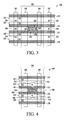
- FIG. 3 is an example embodiment of a top view for a control-gate strap and an associated contact landing region using a dummy select gate structure and a non-patterned spacer gate etch.
- FIG. 4 is a further example embodiment where select gate tabs are used to expand select gate landing regions associated with a strap connection.
- FIGS. 5A-C are example embodiments of cross-section views for formation of an end cell control-gate wrap connection and an associated contact landing region adjacent two select gate lines using a dummy select gate structure and a non-patterned spacer gate etch.
- FIGS. 6A-B are example embodiments of top views for an end cell wrap connection and an associated contact landing region adjacent two select gate lines using a dummy select gate structure and a non-patterned spacer gate etch.
- FIG. 7 is a further example embodiment where an additional dummy select gate structure is used to form larger contact landing regions associated with the wrap connection.
- FIG. 8 provides an example process flow diagram for using dummy select gate structures and a non-patterned spacer gate etch to form improved contact landing regions.
- FIG. 9 is a diagram of an embodiment for wordline driver and column driver connections associated with a split-gate NVM cell.
- a dummy select gate structure is formed while also forming select gate structures for split-gate NVM cells.
- a control gate layer is formed over the select gate structures and the dummy select gate structure, as well as an intervening charge storage layer. The control gate material will fill in gaps between the select gate material and the dummy select gate material.
- a non-patterned spacer etch is then used to etch the control gate layer to form a contact landing region associated with the dummy select gate structure while also forming spacer control gate structures for the split-gate NVM cells.
- the contact landing regions can be used for making electrical connections within the resulting split-gate NVM cell array.
- the embodiments described herein provide improved (e.g., more planar) contact landing regions without requiring additional processing steps and without increasing the pitch of the resulting NVM cell array.
- Different features and variations can be implemented, as desired, and related or modified systems and methods can be utilized, as well.
- Processing steps for split-gate NVM cells can leave non-planar surfaces that cause difficulties in later making good quality electrical connections. For example, if control gates for split-gate NVM cells were formed using a non-patterned spacer gate etch processing step, well-defined lithographic contact landing areas associated with the control gate structures would not be readily available without additional masking steps that increase costs and processing time.
- FIG. 1 is a cross-section view of an embodiment 100 for select gate and control gate structures for a split-gate non-volatile memory (NVM) cell array where a non-patterned spacer gate etch has been used to form control gate structures 112 / 122 .
- one split-gate NVM structure includes select gate (SG) structure 110 , select-gate dielectric (e.g., oxide) layer 111 , charge storage layer 114 , and control gate (CG) structure 112 that are each formed over substrate 102 .
- Another split-gate NVM cell structure includes select gate (SG) structure 120 , select-gate dielectric (e.g., oxide) layer 121 charge storage layer 124 , and control gate (CG) structure 122 that are each formed over substrate 102 .
- select gate structures 110 / 120 will tend to be good quality electrical connections as select gate structures 110 / 120 are well-defined structures (e.g., formed using mask layers).
- control gate structures 112 / 122 were formed using a non-patterned spacer etch processing step without mask layers, control gate structure 112 / 122 are left with non-planar curved surfaces as shown by arrows 150 .
- the area available for contact landing is determined by the spacer control gate length without the ability to be adjusted to meet design rules.
- the electrical contacts made to control gate structures 112 / 122 will tend to form poor quality electrical connections, for example, if alignment is not exact or if gate length is too short.
- Dummy select gate structures are formed at the same time as other select gate structures to allow subsequent control gate layers to form improved landing regions to which electrical contacts can be made in later processing steps.
- a dummy select gate structure is added between select gate lines to provide a sidewall for formation of a control-gate strap and an associated contact landing region without an added mask.
- the control gate material fills in the areas between the select gate structures and the dummy select gate structure, and sufficient control gate material remains after a non-patterned spacer etch to create the control-gate strap connection and the contact landing region for a control gate contact.
- dummy select gate material is located at the longitudinal end of the NVM cell array to provide a sidewall for formation of a wrap connection between two control-gate lines and an associated contact landing region.
- the control gate material fills in areas between the end of two select gate lines and the dummy select gate structures, and sufficient control gate material remains after a non-patterned spacer etch to form the control-gate wrap connection and the contact landing region for end cell contact.
- the dummy select gate structures are located on field oxide and are not electrically contacted. It is further noted that the dummy select gate structures described herein are non-active additional structures that are formed using the processing steps that are used to form select gate structures for active split-gate cells within the split-gate NVM cell array. Variations and additional embodiments can also be implemented, as desired.
- FIGS. 2A-E provide example cross-section views for formation of a control-gate strap and associated contact landing region between two select gate structures using a dummy select gate structure.
- FIG. 3 provides an example top view for formation of the control-gate strap and associated contact landing region.
- FIG. 4 provides a top view for a further example where tabs are used to expand the select gate landing region.
- FIGS. 5A-C provide example cross-section views for formation of the control gate wrap connection and associated contact landing region using a dummy select gate structure.
- FIGS. 6A-B provide an example top view for formation of the end cell wrap connection and associated contact landing region.
- FIG. 7 provides a top view for a further example where additional dummy select gate material is used to form larger contact regions associated with the wrap connection.
- FIG. 8 provides an example process flow embodiment.
- FIG. 9 provides example connections to a split-gate NVM cell. It is further noted that the drawings provide representative embodiment and are not necessarily drawn to exact scale.
- FIGS. 2A-E example cross-section views are shown for formation of a control-gate strap and associated contact landing region between two select gate lines.
- FIG. 2A is a cross-section view of an embodiment 200 after a select gate processing step.
- select gate (SG) structure 110 for one select gate line and select gate (SG) structure 120 for another select gate line have been formed over substrate 102 , along with intervening dielectric layers 111 and 121 .
- a dummy select gate (DSG) structure 210 and a dielectric layer 211 have also been formed while the select structures 110 / 120 and dielectric layers 111 / 121 were being formed.
- the dummy select gate structure 210 is formed using the same material and processing steps as used to form the select structures 110 / 120 .
- a protective dielectric layer was formed over the select gate layer prior to etching of the select gate layer to form select structures 110 / 120 and dummy select gate structure 210 .
- protective layers 204 , 205 , and 206 remain for embodiment 200 , and these protective layers 204 , 205 , and 206 act as optical patterning layers and hard mask for future etches.
- the select structures 110 / 120 can be formed using doped polysilicon or other conductive material, as desired. Further, this select gate material can be deposited, patterned, and etched to form well-defined structures, if desired. Different and/or additional processing steps could also be utilized if desired. It is also noted that the dielectric layers 111 , 121 , and 211 can be, for example, an oxide layer. The protective layers 204 , 205 , and 206 can be, for example, a nitride layer.
- the protective nitride layer can be about 10-30 nm; the select gate and dummy select gate polysilicon layers can be about 100-200 nm, and the oxide dielectric layer can be about 2-5 nm.
- the semiconductor substrate 102 described herein can be any desired semiconductor material or combinations of materials, such as gallium arsenide, silicon germanium, silicon, monocrystalline silicon, other semiconductor materials, and combinations of these semiconductor materials. It is also noted that the semiconductor substrate 102 represents the top portion of a semiconductor substrate.
- semiconductor substrate 102 described herein could be formed on top of other substrate materials including a separate non-semiconductor material, if desired, such as thin film semiconductor substrates formed on other semiconductor or non-semiconductor materials. Further variations could also be implemented, as desired.
- FIG. 2B is a cross-section view of an embodiment 220 after a control gate layer has been formed.
- an intervening charge storage layer 214 has previously been formed over the select structures 110 / 120 .
- the control gate layer 222 is then formed over the select structures 110 / 120 and charge storage layer 214 .
- placement of the dummy select gate structure 210 relatively close to the select structures 110 / 120 causes the control gate material to cover the dummy select gate structure 210 and to fill in the areas between the dummy select gate structure 210 and the select structures 110 / 120 . Without the dummy select gate structure 210 , the control gate material would drop much closer to the substrate 102 as indicated by dashed line 225 .
- the spacing of the dummy select gate structure 210 from the select structures 110 / 120 is dependent on the select gate and control gate material thicknesses. As one example, the distance from the edges of the dummy select gate structure 210 to the select structures 110 / 120 , respectively, can be made to be equal to or less than about 1.5-2.0 times the thickness of the control gate layer. Further, it is noted that the select structures 110 / 120 can be spaced apart by about 4-5 times the thickness of the control gate layer. Other variations and dimensions could also be utilized, as desired, while still allowing the control gate material to fill in the gaps between select-gate structures and dummy select-gate structures.
- control gate material 222 can be formed using doped polysilicon or other conductive material, as desired. Further, for 90 nanometer (nm) processing technology, the control gate polysilicon layer can be about 100-200 nm. Further, this control gate material can be deposited and then etched using a non-patterned spacer gate etch. As described herein, the non-patterned spacer etch does not utilize prior patterning masks for the control gate layer, and the resulting spacer gate structures will not have well-defined vertical edges. Different and/or additional processing steps or variations could also be used with respect to formation of the control gate layer, as desired.
- the charge storage layer 214 can be formed, for example, using silicon nanocrystals, metal nanoclusters, nitride or some other desired discrete charge storage material that is electrically insulated from the top and bottom gates such as by embedding in a dielectric such as oxide.
- a dielectric such as oxide.
- an oxide layer can first be grown followed by formation of a layer of nanocrystals. An additional oxide layer can then be formed on top of the nanocrystal layer thereby resulting in nanocrystals embedded between oxide layers.
- the portions of the charge storage layer 214 that are above these nitride layers will have nanocrystals on top of the nitride layers with a top oxide layer and no initial oxide layer.
- Other variations could also be used, if desired.
- FIG. 2C is a cross-section view of an embodiment 250 after a non-patterned spacer etch has been used to etch the control gate layer 222 .
- the control gate layer 222 is etched to form a control-gate strap between two select gate structures including control gate regions 252 and 256 .
- control gate region 252 has been formed with respect to select gate structure 110 , and the material for the control gate region 252 extends to the dummy select gate structure 210 .
- control gate region 256 has been formed with respect to select gate structure 120 , and the material for the control gate region 256 extends to the dummy select gate structure 210 .
- parasitic (or redundant) spacer control gate regions 254 and 258 also remain after the non-patterned spacer etch has been applied to the control gate layer 222 .
- improved contact landing regions e.g., more planar
- electrical contacts will have better electrical connections due to the improved contact landing regions 270 / 272 that provide a more planar contact surface.
- FIG. 2D is a cross-section view of an embodiment 280 of a patterning and etching step that is utilized to remove the parasitic (or redundant) spacer gate regions 254 and 258 .
- a protective layer 282 e.g., photoresist
- an etch processing step is then utilized to remove the parasitic (or redundant) spacer control gate regions 254 and 258 . It is noted that the parasitic (or redundant) spacer control gate regions 254 and 258 could be left within the resulting NVM cell array, if desired.
- FIG. 2E is a cross-section view of an embodiment 290 after further processing with respect to the strap connection between select gate structures 110 / 120 formed by control gate regions 252 / 256 and dummy select gate structure 210 .
- the protective layer 282 , the nitride layers 204 / 205 / 206 , and portions of the charge storage layer 214 have been removed.
- the nitride layers 204 / 205 / 206 and portions of the charge storage layer 214 under the protective layer 282 in FIG. 2D can be retained, if desired, by removing layer 282 after further processing steps have been used to remove the charge storage layer and nitride layers in the unprotected regions.
- electrical contacts can be made to the contact landing regions 270 / 272 provided by the control gate regions 252 / 256 . As indicated above, these electrical contacts will have better electrical connections due to the improved contact landing regions 270 / 272 that provide a more planar contact surface for the electrical contacts.
- FIGS. 3-4 show a top view for formation of a control-gate strap and associated contact landing regions and that show a top view for using select-gate tabs to expand select gate landing regions, respectively. It is again noted that these top view diagrams provide representative embodiments of only a portion of an NVM cell array and are not necessarily drawn to exact scale.
- FIG. 3 is a top view diagram of an embodiment 300 after a non-patterned spacer gate etch and after patterned etch removal of parasitic control gates.
- the non-patterned spacer gate etch has left control gate strap region 306 and control gate lines 310 , 312 , 314 , and 316 .
- the patterned parasitic etch has removed parasitic control gates in the drain region between select gate lines 321 and 322 and the drain region between select gate lines 323 and 324 .
- active lines 307 represent two of numerous areas of the resulting NVM cell array where active split-gate cells will be formed using the select gate lines 321 , 322 , 323 , and 324 .
- the strap region 309 includes dummy active lines 308 that will not include active split-gate cells.
- dummy select gate (DSG) structure 302 acts to expand the control gate material so that a control-gate strap region 306 between control gate line 312 and control gate line 314 is left after the non-patterned spacer etch.
- this control-gate strap region 306 formed using the dummy select structure 302 also provides improved contact landing regions 340 and 342 , as described herein.
- location 304 represents a location within the improved contact landing region 340 where a contact can be placed in later processing steps to form a connection to the control-gate strap region 306 .
- Locations 332 and 334 represent locations where drain contacts can be placed in later processing steps to form connections to drain regions formed between select gate lines 321 / 322 and 323 / 324 , respectively.
- Locations 336 represents locations where source contacts can be placed in later processing steps to form connections to source regions formed between control gate lines 312 / 314 .
- the select gate lines 322 and 323 can be spaced apart by about 4-5 times the thickness of the control gate layer, and the distance from the edges of the dummy select gate structure 302 to the select gate lines 322 / 323 , respectively, can be made to be equal to or less than about 1.5-2.0 times the thickness of the control gate layer.
- the select gate lines 321 and 322 , as well as select gate lines 323 and 324 can be spaced apart by about 2-3 times the thickness of the control gate layer. Other variations and dimensions could also be utilized, as desired.
- FIG. 4 is a top view diagram of an embodiment 400 where additional dummy select gate material is used to form tabs that provide for larger contact landing areas for select gates.
- additional select gate tabs 402 and 404 have been used to expand the select gate line 322 in a region where an electrical contact may be made as represented by location 412 .
- additional select gate tabs 406 and 408 have been used to expand the select gate line 323 in a region where an electrical contact may be made as represented by location 414 .
- the control-gate strap region 306 will also expand around the select gate tabs 404 and 406 , as shown.
- location 304 represents a possible location for later placement of an electrical contact to the control-gate strap region 306 .
- the improved contact landing regions described herein are formed at the same time that select gate structures and control gate structures are formed for active split-gate NVM cells (not shown) within the active lines 307 for the NVM cell array. With respect to these active split-gate NVM cells, subsequent processing steps can be used to complete the split-gate NVM cells within the active lines 307 . For example, after control gate structures and select gate structures are patterned and etched to form desired structures within the active lines 307 (at which time the improved landing regions are also formed using the dummy select gate structures described herein), source/drain implants can be used to form source regions and drain regions for the active split-gate NVM cells within the active lines 307 .
- interconnect layers can be formed using one or more metal layers, doped polysilicon layers, and/or other desired conductive material layers that are formed, patterned, and etched to create desired interconnect layers.
- processing steps to form the contacts at these locations can include forming a protective layer over the underlying structures including the improved landing regions, forming vias through the protective layer where contacts to the improved landing regions are desired, forming a conductive layer over the protective layer that also fills the vias to provide a contact to the improved landing regions, patterning the conductive layer, and etching the conductive layer to leave a desired interconnect structure. Additional protective layers, vias, and conductive layers can similarly be formed if multiple interconnect layers are desired for the NVM array. Other variations could be implemented, as desired.
- FIGS. 5A-C example cross-section views are shown for formation of the end cell wrap connection and associated contact landing region using a dummy select gate structure and a non-patterned spacer gate etch.
- FIG. 5A is a cross-section view of an embodiment 500 after a select gate processing step.
- select gate (SG) structure 510 has been formed over substrate 102 along with dielectric (e.g., oxide) layer 514 .
- dielectric e.g., oxide
- a dummy select gate (DSG) structure 512 and dielectric (e.g., oxide) layer 516 have also been formed while the select gate structure 510 and dielectric layer 514 were being formed.
- the dummy select gate structure 512 is formed using the same material and processing steps as used to form the select gate structure 510 .
- protective layers 504 and 505 have been formed over the select gate 510 and dummy select gate structure 512 .
- FIG. 5B is a cross-section view of an embodiment 520 after a control gate layer 522 has been formed after formation of an intervening charge storage layer 518 .
- the control gate layer 522 is formed over the previously formed select gate structure 510 , dummy select gate structure 512 , and charge storage layer 518 .
- the dummy select gate structure 512 causes the control gate material to cover the dummy select gate structure 512 and to fill in the gap area between the dummy select gate structure 512 and the select gate structure 510 .
- the control gate material would drop much closer to substrate 102 as indicated by dashed line 525 and would be significantly removed during the spacer etch of the control gate layer 522 .
- the spacing of the dummy select gate structure 512 from the select gate structure 510 is dependent on the select gate and control gate material thicknesses. As one example, the distance from the edge of the dummy select gate structure 512 to the select gate structure 510 can be made to be equal to or less than about 1.5-2.0 times the thickness of the control gate layer. Other variations and dimensions could also be utilized, as desired, while still allowing the control gate material to fill in the gaps between select-gate structures and dummy select-gate structures.
- FIG. 5C is a cross-section view of an embodiment 550 after control gate material in the control gate layer 522 has been etched.
- control gate region 552 extends to the dummy select gate structure 510 and has remained after a non-patterned spacer gate etch has been used to form spacer control gates within the NVM cell array.
- an improved contact landing region that provides a more planar contact surface, as represented by arrow 570 , is formed by the control gate region 552 .
- an electrical contact later made to the control gate material 552 will have a better electrical connection due to the improved contact landing region 570 .
- FIGS. 6A-B and 7 example top views are shown for formation of the end cell wrap connection and associated contact landing region. It is again noted that these top view diagrams provide representative embodiments of only a portion of an NVM cell array and are not necessarily drawn to exact scale.
- FIG. 6A is a top view diagram of an embodiment 600 of an end cell after an initial gate processing step for the formation of the control-gate wrap connection.
- Select gate (SG) lines 321 , 322 , 323 , and 324 have been formed over the semiconductor substrate during a select gate processing step.
- Dummy select gate (DSG) structures 605 , 606 , and 607 represent dummy select gate structures that are also formed during the select gate processing step and are formed at the longitudinal ends of the select gate lines within the array of NVM cells.
- CG control gate
- a non-patterned spacer etch is used to etch the control gate layer in order to form spacer control gates associated with the select gate lines 321 , 322 , 323 , and 324 .
- the control gate regions 610 , 612 , and 614 remain after the spacer etch, and contact landing regions are provided adjacent the dummy select gate structures 605 , 606 , and 607 where electrical contacts can be made, as shown in FIG. 6B .
- active line 307 represents one of numerous areas of the resulting NVM cell array where active split-gate cells will be formed using the select gate lines 321 , 322 , 323 , and 324 .
- several active lines at the edge of the array are typically used as dummy lines for process control. These are identified as dummy active lines 308 within end region 609 .
- FIG. 6B is a top view diagram of an embodiment 650 after parasitic (or redundant) control gates regions have been etched away and electrical contacts have been made.
- portions of the control gate material 610 , 612 , and 614 in FIG. 6A between select gate lines 321 and 322 and between select gate lines 322 and 324 i.e., redundant control gate regions
- Control gate region 661 provides an end cell wrap connection between control gate lines 663 and 664 .
- Locations 652 , 654 , 656 , and 658 represent example locations where contacts can be placed in later processing steps to form connections to the contact landing regions within the control-gate strap regions that have been formed using the dummy select gate structures 605 , 606 , and 607 .
- Locations 332 and 334 represent locations where drain contacts can be placed in later processing steps to form connections to drain regions formed between select gate lines 321 / 322 and 323 / 324 , respectively.
- Location 336 represents a location where a source contact can be placed in later processing steps to form a connection to source regions formed between control gate lines 312 / 314 . It is again noted that the parasitic (or redundant) control gates regions could be left, if desired.
- FIG. 7 is a top view diagram of an embodiment 700 where additional dummy select gate material is used to provide a larger contact landing region associated with the end cell wrap connection.
- additional dummy select gate (DSG) structure 702 has been used to expand the control gate material associated with the end cell wrap connection between control gate lines 663 and 664 .
- the dummy select gate 702 provides for a larger resulting contact landing region, thereby allowing more flexibility for locating electrical contacts, such as at locations 704 and 706 , as compared to locations 656 and 658 in FIG. 6B .
- FIG. 7 is a top view diagram of an embodiment 700 where additional dummy select gate material is used to provide a larger contact landing region associated with the end cell wrap connection.
- DSG dummy select gate
- locations 332 and 334 represent locations where source contacts can be placed in later processing steps to form connections to source regions formed between select gate lines 321 / 322 and 323 / 324 , respectively.
- Location 336 represents a location where a drain contact can be placed in later processing steps to form a connection to drain regions formed between control gate lines 312 / 314 .
- the improved contact landing regions described herein are formed at the same time that select gate structures and control gate structures are formed for active split-gate NVM cells (not shown) within the active regions 307 for the NVM cell array.
- subsequent processing steps can be used to complete the split-gate NVM cells within the active regions 307 .
- source/drain implants can be used to form source regions and drain regions for the active split-gate NVM cells within the active regions 307 .
- interconnect layers can be formed using one or more metal layers, doped polysilicon layers, and/or other desired conductive material layers, along with protective layers and vias, to create desired interconnect layers.
- FIG. 8 a process flow diagram is shown of an embodiment 800 for using dummy select gate structures and a non-patterned spacer etch to form improved contact landing regions for spacer control gate structures without adding additional masks, as described herein.
- select gate structures and at least one dummy select gate structure are formed on a substrate along with a select-gate dielectric layer (e.g., oxide).
- a charge storage layer is formed over the select gates, dummy select gate structure(s), and substrate.
- a control gate layer is formed over the charge storage layer.
- a non-patterned spacer etch is used to etch the control gate layer in order to form spacer control gate structures adjacent to select gate structures within split-gate NVM cells and simultaneously to form at least one contact landing region associated with dummy select gate structure(s).
- one or more electrical contacts are made to the contact landing region(s). It is noted that the different and/or additional processing steps could also be utilized, if desired, in addition to those shown in FIG. 8 . Further, as described above, patterning and etch processing steps can also be used to remove parasitic (or redundant) spacer control gate regions, if desired. Other variations could also be implemented, as desired, while still utilizing dummy select gate structures and a non-patterned spacer etch for a control gate layer to form improved contact landing regions.
- FIG. 9 provides an example embodiment 900 for wordline driver and column driver connections associated with split-gate NVM cell 910 within an array of NVM cells.
- a control-gate voltage V CG
- V CG control-gate voltage
- FIG. 9 provides an example embodiment 900 for wordline driver and column driver connections associated with split-gate NVM cell 910 within an array of NVM cells.
- V CG control-gate voltage
- FIGS. 9 provides an example embodiment 900 for wordline driver and column driver connections associated with split-gate NVM cell 910 within an array of NVM cells.
- V CG control-gate voltage
- V CG control-gate voltage
- These control-gate wordline connections 918 are difficult to achieve with a standard spacer etch process without additional masking.
- a dummy select gate structure and a spacer gate etch can be used to form a control-gate strap and an associated contact landing region between two adjacent control gate lines that are used to form split-gate NVM cells, as shown for example in FIGS.
- a select-gate voltage (V SG ) is provided to the select-gate for NVM cell 910 through connection 916 to a second select-gate wordline 902 .
- a source voltage (V S ) is provided to a source for NVM cell 910 through connection 914 , which is shown as connected to ground 908 for embodiment 900 .
- V D drain voltage
- the column bit-line 906 is coupled to column drivers, and the select-gate wordline 902 and the control-gate wordline 904 are coupled to wordline drivers.
- Other variations could be implemented, as desired.
- Embodiments are described herein for a method for forming a contact landing region for a split-gate non-volatile memory (NVM) system including forming select gate structures for split-gate non-volatile memory (NVM) cells within an array of split-gate NVM cells, forming a dummy select gate structure while forming the select gate structures, forming a charge storage layer for the split-gate NVM cells, forming a control gate layer over the select gate structures and the dummy select gate structure, and etching the control gate layer with a non-patterned spacer etch to form control gate structures associated with the split-gate NVM cells and to form a contact landing region between the select gate structure and the dummy select gate structure.
- NVM split-gate non-volatile memory
- the distance from an edge for the dummy select gate structure to an edge for a select gate structure is equal to or less than about 1.5 to 2.0 times the thickness of the control gate layer.
- the method can include forming an electrical contact coupled to the contact landing region.
- a plurality of dummy select gate structures can be formed, and the etching step can form a plurality of control gate structures and contact landing regions.
- the contact landing region can also include a sloped edge extending from the select gate structure and a sloped edge extending from the dummy select gate structure.
- the dummy select gate structure is formed between two select gate lines within the array of NVM cells. Further, the etching step can leave a control-gate strap between the two select gate lines that includes the dummy select gate structure. In addition, the method can further include forming at least one select-gate tab while forming the select gate structures, the select-gat tab extending from a select gate structure towards the dummy select gate structure.
- the dummy select gate structure can be formed at the longitudinal ends of two select gate lines within the array of NVM cells. Further, the etching step can leave a control-gate wrap connection adjacent the two select gate lines that includes the dummy select gate structure. In addition, the method can further include forming an additional dummy select gate structure between the two select gate lines while forming the select gate structures. Still further, the etching step can leave an additional contact landing region between the dummy select gate structure and the additional dummy select gate structure. Also, the etching step can further leave an additional contact landing region between the additional dummy select gate structure and the select gate structure.
- Embodiments are also disclosed herein for a split-gate non-volatile memory (NVM) cell array including select gate structures formed using a first material layer, dummy select gate structures also formed using the first material layer, control gate structures formed using a second material layer and a non-patterned spacer etch, charge storage layers associated with the select gate structures and the control gate structures, contact landing regions between the dummy select gate structures and the select gate structures where the contact landing regions have been formed using the second material layer and the non-patterned spacer gate etch used to form the control gate structures. Further, electrical contacts can be coupled to the contact landing regions.
- NVM non-volatile memory
- the first material layer and the second material layer include doped polysilicon. Still further, for each dummy select gate structure, a distance from an edge for the dummy select gate structure to an edge for a select gate structure is equal to or less than about 1.5 to 2.0 times the thickness of the control gate layer.
- the contact landing regions can include sloped edges extending from select gate structures and sloped edges extending from dummy select gate structures.
- At least one dummy select gate structure can be located between two select gate lines for the split-gate NVM cell array. Further, at least one contact landing region can be associated with a control-gate strap between the two select gate lines, the control-gate strap including the dummy select gate structure. Still further, at least one select gate tab can be associated with the dummy select gate structure where the select-gat tab extends from the a select gate structure towards a dummy select gate structure and comprising the first material.
- At least one dummy select gate structure can be located at the longitudinal ends of two select gate lines within the split-gate NVM cell array. Further, at least one contact landing region can be associated with a control-gate wrap connection adjacent the two select gate lines, the wrap connection including the dummy select gate structure. Still further, at least one additional dummy select gate structure can be located between the two select gate lines. Also, at least one contact landing region can be associated with the additional dummy select gate structure.
Abstract
Description
Claims (11)
Priority Applications (1)
| Application Number | Priority Date | Filing Date | Title |
|---|---|---|---|
| US14/706,130 US9331092B2 (en) | 2013-09-10 | 2015-05-07 | Methods for forming contact landing regions in split-gate non-volatile memory (NVM) cell arrays |
Applications Claiming Priority (2)
| Application Number | Priority Date | Filing Date | Title |
|---|---|---|---|
| US14/022,646 US9054208B2 (en) | 2013-09-10 | 2013-09-10 | Methods for forming contact landing regions in split-gate non-volatile memory (NVM) cell arrays |
| US14/706,130 US9331092B2 (en) | 2013-09-10 | 2015-05-07 | Methods for forming contact landing regions in split-gate non-volatile memory (NVM) cell arrays |
Related Parent Applications (1)
| Application Number | Title | Priority Date | Filing Date |
|---|---|---|---|
| US14/022,646 Division US9054208B2 (en) | 2013-09-10 | 2013-09-10 | Methods for forming contact landing regions in split-gate non-volatile memory (NVM) cell arrays |
Publications (2)
| Publication Number | Publication Date |
|---|---|
| US20150236035A1 US20150236035A1 (en) | 2015-08-20 |
| US9331092B2 true US9331092B2 (en) | 2016-05-03 |
Family
ID=52624720
Family Applications (2)
| Application Number | Title | Priority Date | Filing Date |
|---|---|---|---|
| US14/022,646 Active 2033-10-16 US9054208B2 (en) | 2013-09-10 | 2013-09-10 | Methods for forming contact landing regions in split-gate non-volatile memory (NVM) cell arrays |
| US14/706,130 Active US9331092B2 (en) | 2013-09-10 | 2015-05-07 | Methods for forming contact landing regions in split-gate non-volatile memory (NVM) cell arrays |
Family Applications Before (1)
| Application Number | Title | Priority Date | Filing Date |
|---|---|---|---|
| US14/022,646 Active 2033-10-16 US9054208B2 (en) | 2013-09-10 | 2013-09-10 | Methods for forming contact landing regions in split-gate non-volatile memory (NVM) cell arrays |
Country Status (1)
| Country | Link |
|---|---|
| US (2) | US9054208B2 (en) |
Families Citing this family (3)
| Publication number | Priority date | Publication date | Assignee | Title |
|---|---|---|---|---|
| US9054208B2 (en) | 2013-09-10 | 2015-06-09 | Freescale Semiconductor, Inc. | Methods for forming contact landing regions in split-gate non-volatile memory (NVM) cell arrays |
| US10879181B2 (en) * | 2016-11-28 | 2020-12-29 | Taiwan Semiconductor Manufacturing Co., Ltd. | Embedded non-volatile memory with side word line |
| CN113013256A (en) * | 2021-02-04 | 2021-06-22 | 上海华力集成电路制造有限公司 | Split-gate MONOS flash memory and manufacturing method thereof |
Citations (6)
| Publication number | Priority date | Publication date | Assignee | Title |
|---|---|---|---|---|
| US6861698B2 (en) | 2002-01-24 | 2005-03-01 | Silicon Storage Technology, Inc. | Array of floating gate memory cells having strap regions and a peripheral logic device region |
| US7227217B2 (en) | 2003-07-18 | 2007-06-05 | Silicon Storage Technology, Inc. | Nonvolatile memory cell having floating gate, control gate and separate erase gate, an array of such memory cells, and method of manufacturing |
| US20090309153A1 (en) | 2008-06-13 | 2009-12-17 | Renesas Technology Corp. | Method of manufacturing semiconductor device and semiconductor device |
| US7936611B2 (en) * | 2006-11-03 | 2011-05-03 | Samsung Electronics Co., Ltd. | Memory device and method of operating and fabricating the same |
| US20120068264A1 (en) | 2010-09-21 | 2012-03-22 | International Business Machines Corporation | Forming narrow fins for finfet devices using asymmetrically spaced mandrels |
| US20150069490A1 (en) | 2013-09-10 | 2015-03-12 | Jane A. Yater | Methods For Forming Contact Landing Regions In Split-Gate Non-Volatile Memory (NVM) Cell Arrays |
-
2013
- 2013-09-10 US US14/022,646 patent/US9054208B2/en active Active
-
2015
- 2015-05-07 US US14/706,130 patent/US9331092B2/en active Active
Patent Citations (6)
| Publication number | Priority date | Publication date | Assignee | Title |
|---|---|---|---|---|
| US6861698B2 (en) | 2002-01-24 | 2005-03-01 | Silicon Storage Technology, Inc. | Array of floating gate memory cells having strap regions and a peripheral logic device region |
| US7227217B2 (en) | 2003-07-18 | 2007-06-05 | Silicon Storage Technology, Inc. | Nonvolatile memory cell having floating gate, control gate and separate erase gate, an array of such memory cells, and method of manufacturing |
| US7936611B2 (en) * | 2006-11-03 | 2011-05-03 | Samsung Electronics Co., Ltd. | Memory device and method of operating and fabricating the same |
| US20090309153A1 (en) | 2008-06-13 | 2009-12-17 | Renesas Technology Corp. | Method of manufacturing semiconductor device and semiconductor device |
| US20120068264A1 (en) | 2010-09-21 | 2012-03-22 | International Business Machines Corporation | Forming narrow fins for finfet devices using asymmetrically spaced mandrels |
| US20150069490A1 (en) | 2013-09-10 | 2015-03-12 | Jane A. Yater | Methods For Forming Contact Landing Regions In Split-Gate Non-Volatile Memory (NVM) Cell Arrays |
Also Published As
| Publication number | Publication date |
|---|---|
| US20150069490A1 (en) | 2015-03-12 |
| US9054208B2 (en) | 2015-06-09 |
| US20150236035A1 (en) | 2015-08-20 |
Similar Documents
| Publication | Publication Date | Title |
|---|---|---|
| US7604926B2 (en) | Method of manufacturing a semiconductor device | |
| US9355913B2 (en) | 3D semiconductor devices and methods of fabricating same | |
| US7585724B2 (en) | FLASH memory device and method of manufacture | |
| US11094595B2 (en) | Memory arrays and methods used in forming a memory array comprising strings of memory cells | |
| KR20090132312A (en) | Highly integrated semiconductor device and method for manufacturing the same | |
| JP2002280467A (en) | Sonos flash memory element and its fabricating method | |
| EP3178111B1 (en) | Split-gate flash memory cell with improved scaling using enhanced lateral control gate to floating gate coupling | |
| US11778816B2 (en) | Etch method for opening a source line in flash memory | |
| US9331092B2 (en) | Methods for forming contact landing regions in split-gate non-volatile memory (NVM) cell arrays | |
| US20170243818A1 (en) | Semiconductor device and manufacturing method thereof | |
| JP2022070982A (en) | Embedded non-volatile memory device and fabrication method of the same | |
| US9613972B1 (en) | Method of manufacturing semiconductor device | |
| US20100176433A1 (en) | Semiconductor device and method of manufacturing the same | |
| US8610192B2 (en) | Non-volatile memory devices having charge storage layers at intersecting locations of word lines and active regions | |
| US7674679B2 (en) | Manufacturing method of semiconductor device and semiconductor device | |
| JP2003282745A (en) | Semiconductor memory device | |
| US20120153374A1 (en) | Semiconductor device and method of manufacturing the same | |
| US20240029794A1 (en) | Memory Circuitry And Method Used In Forming Memory Circuitry | |
| US20240029795A1 (en) | Memory Circuitry And Method Used In Forming Memory Circuitry | |
| US7851304B2 (en) | Nonvolatile memory device and fabrication method | |
| CN106960848A (en) | The preparation method of separate gate flash memory unit interconnection | |
| US6953752B1 (en) | Reduced silicon gouging and common source line resistance in semiconductor devices | |
| US20150214062A1 (en) | Methods For Extending Floating Gates For NVM Cells To Form Sub-Lithographic Features And Related NVM Cells | |
| US20080020530A1 (en) | Manufacturing method of semiconductor device and semiconductor device |
Legal Events
| Date | Code | Title | Description |
|---|---|---|---|
| AS | Assignment |
Owner name: FREESCALE SEMICONDUCTOR, INC., TEXAS Free format text: ASSIGNMENT OF ASSIGNORS INTEREST;ASSIGNORS:YATER, JANE A.;HONG, CHEONG MIN;KANG, SUNG-TAEG;REEL/FRAME:035584/0198 Effective date: 20130909 |
|
| AS | Assignment |
Owner name: CITIBANK, N.A., AS NOTES COLLATERAL AGENT, NEW YORK Free format text: SUPPLEMENT TO IP SECURITY AGREEMENT;ASSIGNOR:FREESCALE SEMICONDUCTOR, INC.;REEL/FRAME:036284/0339 Effective date: 20150724 Owner name: CITIBANK, N.A., AS NOTES COLLATERAL AGENT, NEW YORK Free format text: SUPPLEMENT TO IP SECURITY AGREEMENT;ASSIGNOR:FREESCALE SEMICONDUCTOR, INC.;REEL/FRAME:036284/0363 Effective date: 20150724 Owner name: CITIBANK, N.A., AS NOTES COLLATERAL AGENT, NEW YORK Free format text: SUPPLEMENT TO IP SECURITY AGREEMENT;ASSIGNOR:FREESCALE SEMICONDUCTOR, INC.;REEL/FRAME:036284/0105 Effective date: 20150724 Owner name: CITIBANK, N.A., AS NOTES COLLATERAL AGENT, NEW YOR Free format text: SUPPLEMENT TO IP SECURITY AGREEMENT;ASSIGNOR:FREESCALE SEMICONDUCTOR, INC.;REEL/FRAME:036284/0363 Effective date: 20150724 Owner name: CITIBANK, N.A., AS NOTES COLLATERAL AGENT, NEW YOR Free format text: SUPPLEMENT TO IP SECURITY AGREEMENT;ASSIGNOR:FREESCALE SEMICONDUCTOR, INC.;REEL/FRAME:036284/0105 Effective date: 20150724 Owner name: CITIBANK, N.A., AS NOTES COLLATERAL AGENT, NEW YOR Free format text: SUPPLEMENT TO IP SECURITY AGREEMENT;ASSIGNOR:FREESCALE SEMICONDUCTOR, INC.;REEL/FRAME:036284/0339 Effective date: 20150724 |
|
| AS | Assignment |
Owner name: FREESCALE SEMICONDUCTOR, INC., TEXAS Free format text: PATENT RELEASE;ASSIGNOR:CITIBANK, N.A., AS COLLATERAL AGENT;REEL/FRAME:037357/0859 Effective date: 20151207 |
|
| AS | Assignment |
Owner name: MORGAN STANLEY SENIOR FUNDING, INC., MARYLAND Free format text: ASSIGNMENT AND ASSUMPTION OF SECURITY INTEREST IN PATENTS;ASSIGNOR:CITIBANK, N.A.;REEL/FRAME:037565/0510 Effective date: 20151207 Owner name: MORGAN STANLEY SENIOR FUNDING, INC., MARYLAND Free format text: ASSIGNMENT AND ASSUMPTION OF SECURITY INTEREST IN PATENTS;ASSIGNOR:CITIBANK, N.A.;REEL/FRAME:037565/0527 Effective date: 20151207 |
|
| AS | Assignment |
Owner name: MORGAN STANLEY SENIOR FUNDING, INC., MARYLAND Free format text: SECURITY AGREEMENT SUPPLEMENT;ASSIGNOR:NXP B.V.;REEL/FRAME:038017/0058 Effective date: 20160218 |
|
| STCF | Information on status: patent grant |
Free format text: PATENTED CASE |
|
| AS | Assignment |
Owner name: MORGAN STANLEY SENIOR FUNDING, INC., MARYLAND Free format text: SUPPLEMENT TO THE SECURITY AGREEMENT;ASSIGNOR:FREESCALE SEMICONDUCTOR, INC.;REEL/FRAME:039138/0001 Effective date: 20160525 |
|
| AS | Assignment |
Owner name: MORGAN STANLEY SENIOR FUNDING, INC., MARYLAND Free format text: CORRECTIVE ASSIGNMENT TO CORRECT THE REMOVE APPLICATION 12092129 PREVIOUSLY RECORDED ON REEL 038017 FRAME 0058. ASSIGNOR(S) HEREBY CONFIRMS THE SECURITY AGREEMENT SUPPLEMENT;ASSIGNOR:NXP B.V.;REEL/FRAME:039361/0212 Effective date: 20160218 |
|
| AS | Assignment |
Owner name: NXP, B.V., F/K/A FREESCALE SEMICONDUCTOR, INC., NETHERLANDS Free format text: RELEASE BY SECURED PARTY;ASSIGNOR:MORGAN STANLEY SENIOR FUNDING, INC.;REEL/FRAME:040925/0001 Effective date: 20160912 Owner name: NXP, B.V., F/K/A FREESCALE SEMICONDUCTOR, INC., NE Free format text: RELEASE BY SECURED PARTY;ASSIGNOR:MORGAN STANLEY SENIOR FUNDING, INC.;REEL/FRAME:040925/0001 Effective date: 20160912 |
|
| AS | Assignment |
Owner name: NXP B.V., NETHERLANDS Free format text: RELEASE BY SECURED PARTY;ASSIGNOR:MORGAN STANLEY SENIOR FUNDING, INC.;REEL/FRAME:040928/0001 Effective date: 20160622 |
|
| AS | Assignment |
Owner name: NXP USA, INC., TEXAS Free format text: MERGER;ASSIGNOR:FREESCALE SEMICONDUCTOR, INC.;REEL/FRAME:041144/0363 Effective date: 20161107 |
|
| AS | Assignment |
Owner name: MORGAN STANLEY SENIOR FUNDING, INC., MARYLAND Free format text: CORRECTIVE ASSIGNMENT TO CORRECT THE REMOVE APPLICATION 12681366 PREVIOUSLY RECORDED ON REEL 039361 FRAME 0212. ASSIGNOR(S) HEREBY CONFIRMS THE SECURITY AGREEMENT SUPPLEMENT;ASSIGNOR:NXP B.V.;REEL/FRAME:042762/0145 Effective date: 20160218 Owner name: MORGAN STANLEY SENIOR FUNDING, INC., MARYLAND Free format text: CORRECTIVE ASSIGNMENT TO CORRECT THE REMOVE APPLICATION 12681366 PREVIOUSLY RECORDED ON REEL 038017 FRAME 0058. ASSIGNOR(S) HEREBY CONFIRMS THE SECURITY AGREEMENT SUPPLEMENT;ASSIGNOR:NXP B.V.;REEL/FRAME:042985/0001 Effective date: 20160218 |
|
| AS | Assignment |
Owner name: NXP B.V., NETHERLANDS Free format text: RELEASE BY SECURED PARTY;ASSIGNOR:MORGAN STANLEY SENIOR FUNDING, INC.;REEL/FRAME:050744/0097 Effective date: 20190903 Owner name: NXP B.V., NETHERLANDS Free format text: RELEASE BY SECURED PARTY;ASSIGNOR:MORGAN STANLEY SENIOR FUNDING, INC.;REEL/FRAME:050745/0001 Effective date: 20190903 |
|
| MAFP | Maintenance fee payment |
Free format text: PAYMENT OF MAINTENANCE FEE, 4TH YEAR, LARGE ENTITY (ORIGINAL EVENT CODE: M1551); ENTITY STATUS OF PATENT OWNER: LARGE ENTITY Year of fee payment: 4 |
|
| AS | Assignment |
Owner name: MORGAN STANLEY SENIOR FUNDING, INC., MARYLAND Free format text: CORRECTIVE ASSIGNMENT TO CORRECT THE REMOVE APPLICATION 12298143 PREVIOUSLY RECORDED ON REEL 042762 FRAME 0145. ASSIGNOR(S) HEREBY CONFIRMS THE SECURITY AGREEMENT SUPPLEMENT;ASSIGNOR:NXP B.V.;REEL/FRAME:051145/0184 Effective date: 20160218 Owner name: MORGAN STANLEY SENIOR FUNDING, INC., MARYLAND Free format text: CORRECTIVE ASSIGNMENT TO CORRECT THE REMOVE APPLICATION 12298143 PREVIOUSLY RECORDED ON REEL 039361 FRAME 0212. ASSIGNOR(S) HEREBY CONFIRMS THE SECURITY AGREEMENT SUPPLEMENT;ASSIGNOR:NXP B.V.;REEL/FRAME:051029/0387 Effective date: 20160218 Owner name: MORGAN STANLEY SENIOR FUNDING, INC., MARYLAND Free format text: CORRECTIVE ASSIGNMENT TO CORRECT THE REMOVE APPLICATION 12298143 PREVIOUSLY RECORDED ON REEL 042985 FRAME 0001. ASSIGNOR(S) HEREBY CONFIRMS THE SECURITY AGREEMENT SUPPLEMENT;ASSIGNOR:NXP B.V.;REEL/FRAME:051029/0001 Effective date: 20160218 Owner name: MORGAN STANLEY SENIOR FUNDING, INC., MARYLAND Free format text: CORRECTIVE ASSIGNMENT TO CORRECT THE REMOVE APPLICATION 12298143 PREVIOUSLY RECORDED ON REEL 038017 FRAME 0058. ASSIGNOR(S) HEREBY CONFIRMS THE SECURITY AGREEMENT SUPPLEMENT;ASSIGNOR:NXP B.V.;REEL/FRAME:051030/0001 Effective date: 20160218 Owner name: MORGAN STANLEY SENIOR FUNDING, INC., MARYLAND Free format text: CORRECTIVE ASSIGNMENT TO CORRECT THE REMOVE APPLICATION12298143 PREVIOUSLY RECORDED ON REEL 042985 FRAME 0001. ASSIGNOR(S) HEREBY CONFIRMS THE SECURITY AGREEMENT SUPPLEMENT;ASSIGNOR:NXP B.V.;REEL/FRAME:051029/0001 Effective date: 20160218 Owner name: MORGAN STANLEY SENIOR FUNDING, INC., MARYLAND Free format text: CORRECTIVE ASSIGNMENT TO CORRECT THE REMOVE APPLICATION12298143 PREVIOUSLY RECORDED ON REEL 039361 FRAME 0212. ASSIGNOR(S) HEREBY CONFIRMS THE SECURITY AGREEMENT SUPPLEMENT;ASSIGNOR:NXP B.V.;REEL/FRAME:051029/0387 Effective date: 20160218 Owner name: MORGAN STANLEY SENIOR FUNDING, INC., MARYLAND Free format text: CORRECTIVE ASSIGNMENT TO CORRECT THE REMOVE APPLICATION12298143 PREVIOUSLY RECORDED ON REEL 042762 FRAME 0145. ASSIGNOR(S) HEREBY CONFIRMS THE SECURITY AGREEMENT SUPPLEMENT;ASSIGNOR:NXP B.V.;REEL/FRAME:051145/0184 Effective date: 20160218 |
|
| AS | Assignment |
Owner name: NXP B.V., NETHERLANDS Free format text: CORRECTIVE ASSIGNMENT TO CORRECT THE REMOVEAPPLICATION 11759915 AND REPLACE IT WITH APPLICATION11759935 PREVIOUSLY RECORDED ON REEL 040928 FRAME 0001. ASSIGNOR(S) HEREBY CONFIRMS THE RELEASE OF SECURITYINTEREST;ASSIGNOR:MORGAN STANLEY SENIOR FUNDING, INC.;REEL/FRAME:052915/0001 Effective date: 20160622 |
|
| AS | Assignment |
Owner name: NXP, B.V. F/K/A FREESCALE SEMICONDUCTOR, INC., NETHERLANDS Free format text: CORRECTIVE ASSIGNMENT TO CORRECT THE REMOVEAPPLICATION 11759915 AND REPLACE IT WITH APPLICATION11759935 PREVIOUSLY RECORDED ON REEL 040925 FRAME 0001. ASSIGNOR(S) HEREBY CONFIRMS THE RELEASE OF SECURITYINTEREST;ASSIGNOR:MORGAN STANLEY SENIOR FUNDING, INC.;REEL/FRAME:052917/0001 Effective date: 20160912 |
|
| MAFP | Maintenance fee payment |
Free format text: PAYMENT OF MAINTENANCE FEE, 8TH YEAR, LARGE ENTITY (ORIGINAL EVENT CODE: M1552); ENTITY STATUS OF PATENT OWNER: LARGE ENTITY Year of fee payment: 8 |