US9362903B2 - Gate drivers for circuits based on semiconductor devices - Google Patents

Gate drivers for circuits based on semiconductor devices Download PDF

Info

Publication number
US9362903B2
US9362903B2 US14/708,627 US201514708627A US9362903B2 US 9362903 B2 US9362903 B2 US 9362903B2 US 201514708627 A US201514708627 A US 201514708627A US 9362903 B2 US9362903 B2 US 9362903B2
Authority
US
United States
Prior art keywords
voltage
switching device
gate
gate driver
switching
Prior art date
Legal status (The legal status is an assumption and is not a legal conclusion. Google has not performed a legal analysis and makes no representation as to the accuracy of the status listed.)
Active
Application number
US14/708,627
Other versions
US20150249447A1 (en
Inventor
Yifeng Wu
Liang Zhou
Zhan Wang
Current Assignee (The listed assignees may be inaccurate. Google has not performed a legal analysis and makes no representation or warranty as to the accuracy of the list.)
Transphorm Technology Inc
Original Assignee
Transphorm Inc
Priority date (The priority date is an assumption and is not a legal conclusion. Google has not performed a legal analysis and makes no representation as to the accuracy of the date listed.)
Filing date
Publication date
Application filed by Transphorm Inc filed Critical Transphorm Inc
Priority to US14/708,627 priority Critical patent/US9362903B2/en
Assigned to TRANSPHORM INC. reassignment TRANSPHORM INC. ASSIGNMENT OF ASSIGNORS INTEREST (SEE DOCUMENT FOR DETAILS). Assignors: WANG, ZHAN, WU, YIFENG, ZHOU, LIANG
Publication of US20150249447A1 publication Critical patent/US20150249447A1/en
Application granted granted Critical
Publication of US9362903B2 publication Critical patent/US9362903B2/en
Assigned to NEXPERIA B.V. reassignment NEXPERIA B.V. SECURITY INTEREST (SEE DOCUMENT FOR DETAILS). Assignors: TRANSPHORM, INC.
Assigned to TRANSPHORM TECHNOLOGY, INC. reassignment TRANSPHORM TECHNOLOGY, INC. CHANGE OF NAME (SEE DOCUMENT FOR DETAILS). Assignors: TRANSPHORM, INC.
Assigned to RENESAS ELECTRONICS AMERICA INC. reassignment RENESAS ELECTRONICS AMERICA INC. SECURITY INTEREST (SEE DOCUMENT FOR DETAILS). Assignors: TRANSPHORM TECHNOLOGY, INC., TRANSPHORM, INC.
Active legal-status Critical Current
Anticipated expiration legal-status Critical

Links

Images

Classifications

    • HELECTRICITY
    • H03ELECTRONIC CIRCUITRY
    • H03KPULSE TECHNIQUE
    • H03K17/00Electronic switching or gating, i.e. not by contact-making and –breaking
    • H03K17/16Modifications for eliminating interference voltages or currents
    • H03K17/161Modifications for eliminating interference voltages or currents in field-effect transistor switches
    • H03K17/162Modifications for eliminating interference voltages or currents in field-effect transistor switches without feedback from the output circuit to the control circuit
    • HELECTRICITY
    • H01ELECTRIC ELEMENTS
    • H01LSEMICONDUCTOR DEVICES NOT COVERED BY CLASS H10
    • H01L21/00Processes or apparatus adapted for the manufacture or treatment of semiconductor or solid state devices or of parts thereof
    • H01L21/02Manufacture or treatment of semiconductor devices or of parts thereof
    • H01L21/04Manufacture or treatment of semiconductor devices or of parts thereof the devices having at least one potential-jump barrier or surface barrier, e.g. PN junction, depletion layer or carrier concentration layer
    • H01L21/18Manufacture or treatment of semiconductor devices or of parts thereof the devices having at least one potential-jump barrier or surface barrier, e.g. PN junction, depletion layer or carrier concentration layer the devices having semiconductor bodies comprising elements of Group IV of the Periodic System or AIIIBV compounds with or without impurities, e.g. doping materials
    • H01L21/28Manufacture of electrodes on semiconductor bodies using processes or apparatus not provided for in groups H01L21/20 - H01L21/268
    • H01L21/28008Making conductor-insulator-semiconductor electrodes
    • H01L21/28264Making conductor-insulator-semiconductor electrodes the insulator being formed after the semiconductor body, the semiconductor being a III-V compound
    • HELECTRICITY
    • H01ELECTRIC ELEMENTS
    • H01LSEMICONDUCTOR DEVICES NOT COVERED BY CLASS H10
    • H01L29/00Semiconductor devices adapted for rectifying, amplifying, oscillating or switching, or capacitors or resistors with at least one potential-jump barrier or surface barrier, e.g. PN junction depletion layer or carrier concentration layer; Details of semiconductor bodies or of electrodes thereof  ; Multistep manufacturing processes therefor
    • H01L29/02Semiconductor bodies ; Multistep manufacturing processes therefor
    • H01L29/12Semiconductor bodies ; Multistep manufacturing processes therefor characterised by the materials of which they are formed
    • H01L29/20Semiconductor bodies ; Multistep manufacturing processes therefor characterised by the materials of which they are formed including, apart from doping materials or other impurities, only AIIIBV compounds
    • H01L29/2003Nitride compounds
    • HELECTRICITY
    • H01ELECTRIC ELEMENTS
    • H01LSEMICONDUCTOR DEVICES NOT COVERED BY CLASS H10
    • H01L29/00Semiconductor devices adapted for rectifying, amplifying, oscillating or switching, or capacitors or resistors with at least one potential-jump barrier or surface barrier, e.g. PN junction depletion layer or carrier concentration layer; Details of semiconductor bodies or of electrodes thereof  ; Multistep manufacturing processes therefor
    • H01L29/40Electrodes ; Multistep manufacturing processes therefor
    • H01L29/402Field plates
    • HELECTRICITY
    • H01ELECTRIC ELEMENTS
    • H01LSEMICONDUCTOR DEVICES NOT COVERED BY CLASS H10
    • H01L29/00Semiconductor devices adapted for rectifying, amplifying, oscillating or switching, or capacitors or resistors with at least one potential-jump barrier or surface barrier, e.g. PN junction depletion layer or carrier concentration layer; Details of semiconductor bodies or of electrodes thereof  ; Multistep manufacturing processes therefor
    • H01L29/40Electrodes ; Multistep manufacturing processes therefor
    • H01L29/41Electrodes ; Multistep manufacturing processes therefor characterised by their shape, relative sizes or dispositions
    • H01L29/423Electrodes ; Multistep manufacturing processes therefor characterised by their shape, relative sizes or dispositions not carrying the current to be rectified, amplified or switched
    • H01L29/42312Gate electrodes for field effect devices
    • H01L29/42316Gate electrodes for field effect devices for field-effect transistors
    • H01L29/4232Gate electrodes for field effect devices for field-effect transistors with insulated gate
    • H01L29/42356Disposition, e.g. buried gate electrode
    • H01L29/4236Disposition, e.g. buried gate electrode within a trench, e.g. trench gate electrode, groove gate electrode
    • HELECTRICITY
    • H01ELECTRIC ELEMENTS
    • H01LSEMICONDUCTOR DEVICES NOT COVERED BY CLASS H10
    • H01L29/00Semiconductor devices adapted for rectifying, amplifying, oscillating or switching, or capacitors or resistors with at least one potential-jump barrier or surface barrier, e.g. PN junction depletion layer or carrier concentration layer; Details of semiconductor bodies or of electrodes thereof  ; Multistep manufacturing processes therefor
    • H01L29/66Types of semiconductor device ; Multistep manufacturing processes therefor
    • H01L29/66007Multistep manufacturing processes
    • H01L29/66075Multistep manufacturing processes of devices having semiconductor bodies comprising group 14 or group 13/15 materials
    • H01L29/66227Multistep manufacturing processes of devices having semiconductor bodies comprising group 14 or group 13/15 materials the devices being controllable only by the electric current supplied or the electric potential applied, to an electrode which does not carry the current to be rectified, amplified or switched, e.g. three-terminal devices
    • H01L29/66409Unipolar field-effect transistors
    • H01L29/66477Unipolar field-effect transistors with an insulated gate, i.e. MISFET
    • H01L29/66522Unipolar field-effect transistors with an insulated gate, i.e. MISFET with an active layer made of a group 13/15 material
    • HELECTRICITY
    • H01ELECTRIC ELEMENTS
    • H01LSEMICONDUCTOR DEVICES NOT COVERED BY CLASS H10
    • H01L29/00Semiconductor devices adapted for rectifying, amplifying, oscillating or switching, or capacitors or resistors with at least one potential-jump barrier or surface barrier, e.g. PN junction depletion layer or carrier concentration layer; Details of semiconductor bodies or of electrodes thereof  ; Multistep manufacturing processes therefor
    • H01L29/66Types of semiconductor device ; Multistep manufacturing processes therefor
    • H01L29/68Types of semiconductor device ; Multistep manufacturing processes therefor controllable by only the electric current supplied, or only the electric potential applied, to an electrode which does not carry the current to be rectified, amplified or switched
    • H01L29/76Unipolar devices, e.g. field effect transistors
    • H01L29/772Field effect transistors
    • H01L29/778Field effect transistors with two-dimensional charge carrier gas channel, e.g. HEMT ; with two-dimensional charge-carrier layer formed at a heterojunction interface
    • H01L29/7786Field effect transistors with two-dimensional charge carrier gas channel, e.g. HEMT ; with two-dimensional charge-carrier layer formed at a heterojunction interface with direct single heterostructure, i.e. with wide bandgap layer formed on top of active layer, e.g. direct single heterostructure MIS-like HEMT
    • HELECTRICITY
    • H03ELECTRONIC CIRCUITRY
    • H03KPULSE TECHNIQUE
    • H03K17/00Electronic switching or gating, i.e. not by contact-making and –breaking
    • H03K17/16Modifications for eliminating interference voltages or currents
    • H03K17/161Modifications for eliminating interference voltages or currents in field-effect transistor switches
    • H03K17/162Modifications for eliminating interference voltages or currents in field-effect transistor switches without feedback from the output circuit to the control circuit
    • H03K17/163Soft switching
    • HELECTRICITY
    • H03ELECTRONIC CIRCUITRY
    • H03KPULSE TECHNIQUE
    • H03K17/00Electronic switching or gating, i.e. not by contact-making and –breaking
    • H03K17/51Electronic switching or gating, i.e. not by contact-making and –breaking characterised by the components used
    • H03K17/56Electronic switching or gating, i.e. not by contact-making and –breaking characterised by the components used by the use, as active elements, of semiconductor devices
    • H03K17/687Electronic switching or gating, i.e. not by contact-making and –breaking characterised by the components used by the use, as active elements, of semiconductor devices the devices being field-effect transistors
    • H03K2017/6875Electronic switching or gating, i.e. not by contact-making and –breaking characterised by the components used by the use, as active elements, of semiconductor devices the devices being field-effect transistors using self-conductive, depletion FETs

Definitions

  • This invention relates to electronic modules formed of semiconductor devices, and specifically to gate drivers for the semiconductor devices.
  • FIG. 1 A prior art circuit schematic of a 3-phase bridge circuit 100 configured to drive a motor is shown in FIG. 1 .
  • Each of the three half bridges 115 , 125 , and 135 in circuit 100 includes two transistors, 141 and 142 , 143 and 144 , and 145 and 146 , respectively, which are able to block voltage in a first direction and are capable of conducting current in the first direction or optionally in both directions.
  • an anti-parallel diode may be connected to each of the transistors 141 - 146 .
  • gate drivers 151 - 156 are each coupled between the gate and source of their respective transistor.
  • Gate drivers 151 - 156 may each be individual circuits.
  • the gate drivers of each half bridge 115 , 125 , and 135 can be integrated into a single gate drive circuit.
  • the gate drivers of all of the transistors 141 - 146 in the bridge circuit can be integrated into a single gate drive circuit.
  • Each of transistors 141 - 146 is capable of blocking a voltage at least as large as the high voltage (HV) source 101 of the circuit 100 when they are biased in the OFF state. That is, when the gate-source voltage VGS applied by the gate drive circuits 151 - 156 to any of transistors 141 - 146 , respectively, is less than the transistor threshold voltage V th , no substantial current flows through the transistor when the drain-source voltage VDS (i.e., the voltage at the drain relative to the source) is between 0V and HV. When biased in the ON state (i.e. with VGS greater than the transistor threshold voltage), the transistors 141 - 146 are each capable of conducting sufficiently high current for the application in which they are used.
  • VGS high voltage
  • blocking a voltage refers to a transistor, device, or component being in a state for which significant current, such as current that is greater than 0.001 times the average operating current during regular ON-state conduction, is prevented from flowing through the transistor, device, or component when a voltage is applied across the transistor, device, or component.
  • significant current such as current that is greater than 0.001 times the average operating current during regular ON-state conduction
  • the total current passing through the transistor, device, or component will not be greater than 0.001 times the average operating current during regular ON-state conduction.
  • the transistors 141 - 146 may be enhancement mode or E-mode transistors (normally off, V th >0), or depletion mode or D-mode (normally on, V th ⁇ 0) transistors.
  • enhancement mode devices are typically used to prevent accidental turn on which may cause damage to the devices or other circuit components.
  • the transistors 141 - 146 can be replaced by a high-voltage D-mode transistor 201 and a low voltage E-mode transistor 202 connected in a cascode configuration 200 , as shown in FIG. 2 .
  • the source 211 of D-mode transistor 201 is connected to the drain 216 of E-mode transistor 202
  • the gate 212 of D-mode transistor 201 is electrically connected or electrically coupled to the source 214 of E-mode transistor 202 .
  • Cascode device 200 is configured to operate as a high-voltage E-mode device, with node 221 functioning as the source, node 222 functioning as the gate, and node 223 functioning as the drain. Referring back to FIG. 1 , nodes 117 , 118 , and 119 are all coupled to one another via inductive loads, i.e., inductive components such as motor coils (not shown in FIG. 1 ).
  • two or more contacts or other items such as conductive layers or components are said to be “electrically connected” if they are connected by a material which is sufficiently conducting to ensure that the electric potential at each of the contacts or other items is substantially the same or about the same regardless of bias conditions.
  • FIG. 3B indicates the path of the current 327 during the time that transistor 141 is biased ON.
  • the motor current flows through transistors 141 and 144 , while no current flows through transistor 142 because transistor 142 is biased OFF, and the voltage at node 117 is close to HV, so transistor 142 blocks a voltage which is close to HV.
  • transistor 141 when transistor 141 is switched OFF, no current can flow through transistor 141 , so the motor current flows in the reverse direction through transistor 142 , which can occur whether transistor 142 is biased ON or OFF.
  • an anti-parallel freewheeling diode (not shown) can be connected across transistor 142 , in which case the reverse current flows through the freewheeling diode.
  • the inductive component 321 forces the voltage at node 117 to a sufficiently negative value to cause reverse conduction through transistor 142 , and transistor 141 blocks a voltage which is close to HV.
  • a hard-switching circuit configuration is one in which the switching transistors are configured to have high currents passing through them as soon as they are switched ON, and to have high voltages across them as soon as they are switched OFF.
  • the transistors are switched ON during periods where non-zero currents flow through the inductive load, so substantial current flows through the transistors immediately or soon after the transistors are switched ON, rather than the current rising gradually.
  • the transistors are switched OFF during periods where high voltages must be blocked by the transistors, so substantial voltage is blocked by the transistors immediately or soon after the transistors are switched OFF, rather than the voltage rising gradually.
  • Transistors switched under these conditions are said to be “hard-switched”.
  • each of the transistors 141 - 146 has a maximum switching rate at which the device can switch from the OFF state to the ON state or vice-versa, the maximum switching rate being largely dependent on the particular switching characteristics of the device, but also partially depending on other adjacent components in the circuit.
  • the switching time for the switching of the voltages at the output nodes 161 - 166 of each of the gate drivers 151 - 156 can be much less than the switching times of each of their respective switching devices 141 - 146 . Consequently, in the configurations of FIGS.
  • the maximum output current that can be supplied by the gate drivers 151 - 156 is chosen to be high.
  • the maximum output current of each of the gate drivers 151 - 156 is typically chosen to be at least 1/60 times the maximum rated output current of each of their respective switching devices 141 - 146 .
  • hard-switched circuits tend to be simple to design and operate, hard-switched components tend to exhibit high levels of electro-magnetic interference (EMI) during operation, in particular in high voltage and/or high current applications in which the switching rate of each of the devices is very high. This can lead to circuit instability or catastrophic failure of the devices in the circuit.
  • EMI electro-magnetic interference
  • the circuit high voltage (HV) is large (e.g., greater than 300V) and/or the switching devices need to switch large currents (e.g., greater than 5 Amps)
  • the circuits exhibit excessively high levels of EMI, become unstable, and cease to function properly.
  • a soft-switching circuit configuration is one in which the switching transistors are configured to be switched ON during zero-current (or near zero-current) conditions and switched OFF during zero-voltage (or near zero-voltage) conditions.
  • Soft-switching methods and configurations have been developed to address the high levels of EMI and associated ringing observed in hard-switched circuits, especially in high current and/or high voltage applications. While soft-switching can in many cases alleviate these problems, the circuitry required for soft switching typically includes many additional components, resulting in increased overall cost and complexity.
  • Soft-switching also typically requires that the circuits be configured to switch only at specific times when the zero-current or zero-voltage conditions are met, hence limiting the control signals that can be applied and in many cases reducing circuit performance.
  • alternative configurations and methods are desirable for power switching circuits in order to maintain sufficiently low levels of EMI while at the same time maintaining circuit stability.
  • high-voltage circuits which include high-voltage switching devices.
  • the gate drivers of the switching devices are configured to reduce the switching rates of the switching devices during operation and improve stability of the high-voltage circuits.
  • an electronic component in a first aspect, includes a switching device comprising a source, a gate, and a drain, the switching device having a predetermined device switching rate.
  • the electronic component further includes a gate driver electrically connected to the gate and coupled between the source and the gate of the switching device, the gate driver configured to switch a gate voltage of the switching device at a gate driver switching rate.
  • the gate driver is configured such that in operation, an output current of the gate driver cannot exceed a first current level, wherein the first current level is sufficiently small to provide a switching rate of the switching device in operation to be less than the predetermined device switching rate.
  • an electronic component in a second aspect, includes a switching device comprising a source, a gate, and a drain, the switching device being operable to block at least 300V when biased OFF.
  • the electronic component further includes a gate driver coupled between the source and the gate of the switching device, the gate driver configured to switch voltage at an output of the gate driver at a gate driver switching rate.
  • a resistance between the output of the gate driver and the gate of the switching device is less than 5 Ohms, and the gate driver is configured such that in operation, an output current of the gate driver is limited by circuitry of the gate driver such that the output current cannot exceed a first current level.
  • a ratio of the first current level to a maximum rated current of the switching device is less than 1/100.
  • a method of operating an electronic component includes a switching device comprising a source, a gate, and a drain, the switching device configured to have a predetermined device current switching rate.
  • the electronic component also includes a gate driver coupled between the source and the gate of the switching device.
  • the method includes causing the gate driver to switch an output voltage of the gate driver from a first state to a second state at a gate driver switching rate, whereby a gate voltage of the switching device is switched at substantially the same rate as the gate driver switching rate, and wherein switching of the output voltage of the gate driver from the first state to the second state causes current through the switching device to be switched at a current switching rate less than the predetermined device current switching rate.
  • a circuit in a fourth aspect, includes a switching device having a maximum rated current and comprising a source, a gate, and a drain.
  • the circuit also includes a first voltage supply which applies an output voltage of at least 300 Volts, and a gate driver connected to a second voltage supply and coupled between the source and the gate of the switching device, the gate driver configured to switch a gate voltage of the switching device at a gate driver switching rate.
  • the gate driver is configured such that in operation, an output current of the gate driver cannot exceed a first current level.
  • the switching device is configured to block the output voltage applied by the first voltage supply during at least a portion of operation of the circuit, a ratio of the first current level to the maximum rated current of the switching device is less than 1/100, and in operation of the circuit, a voltage switching rate of the switching device is greater than 100 Volts/nanosecond.
  • the electronic components, circuits, and methods described herein can include one or more of the following features.
  • the electronic component can be part of a half bridge circuit.
  • the switching device can comprise a III-Nitride transistor.
  • the switching device can comprise an enhancement-mode transistor coupled to a depletion-mode transistor.
  • the depletion-mode transistor and the enhancement-mode transistor can be configured such that a source of the enhancement-mode transistor serves as the source of the switching device, a gate of the enhancement-mode transistor serves as the gate of the switching device, and a drain of the depletion-mode transistor serves as a gate of the switching device.
  • the switching device can be operable to block at least 300V when biased OFF.
  • a maximum rated current of the switching device can be at least 50 Amps.
  • a ratio of the first current level to a maximum rated current of the switching device can be less than 1/100.
  • the switching rate of the switching device in operation can be less than 0.5 times the predetermined device switching rate.
  • the output of the gate driver can be directly connected to the gate of the switching device.
  • the electronic component or circuit can further include a ferrite bead connected between the output of the gate driver and the gate of the switching device.
  • An output of the gate driver can be electrically connected to the gate, and switching the output voltage of the gate driver from the first state to the second state can cause a voltage of at least 300V to be switched across the switching device.
  • a maximum output current of the gate driver can be sufficiently small to cause the current switching rate of the switching device to be less than the predetermined device current switching rate.
  • the circuit can be a half bridge. The half bridge can be connected to an inductive load, wherein in operation, a current greater than 1 Amp passes through the inductive load.
  • the second voltage supply can apply an output voltage that is substantially less than the output voltage of the first voltage supply.
  • the second voltage supply can apply an output voltage less than 25 Volts.
  • An output of the gate driver can be electrically connected to the gate of the switching device.
  • the circuit can further comprise a resistor between an output of the gate driver and the gate of the switching device, wherein the resistor has a resistance between 0 Ohms and 5 Ohms.
  • the switching device can comprise a III-Nitrid
  • FIG. 1 illustrates a circuit schematic of a prior art 3-phase bridge circuit.
  • FIG. 2 is a prior art circuit schematic of two transistors arranged in a cascode configuration.
  • FIGS. 3A-3C illustrate portions of the prior art 3-phase bridge circuit of FIG. 1 under various operating conditions.
  • FIGS. 4-5 illustrate half bridge circuits configured to drive electrical loads.
  • FIG. 6 is a cross-sectional schematic view of a III-Nitride enhancement-mode transistor.
  • FIGS. 7-8 illustrate half bridge circuits configured to drive electrical loads.
  • FIG. 9 is a circuit schematic of a cascode device that can be used as a switching device in the half bridge circuit of FIG. 8 .
  • FIG. 10 is a cross-sectional schematic view of a III-Nitride depletion-mode transistor.
  • FIGS. 11 and 12 are illustrations of bidirectional switches.
  • FIG. 13 is a plot of voltage and current characteristics as a function of time for a switching device of the half bridge circuit of FIG. 8 during circuit operation.
  • Described herein are configurations and methods for slowing the switching rate (i.e., the slew rate) of switching devices utilized in electronic components and circuits.
  • This reduction in switching rate reduces levels of EMI in the circuits during and immediately following switching, thereby allowing for improved circuit stability, in particular in applications where high currents (e.g., 4 Amps or higher) and/or high voltages (e.g., greater than 300V) are being switched by the switching devices.
  • Each of the transistors or other switching devices in the circuits and components described herein can be configured to be hard-switched, as previously described, at a particular switching rate.
  • a transistor of one of the circuits herein When a transistor of one of the circuits herein is in the OFF state with no substantial current flowing through it, it supports a large voltage which can be about equal to or close to the circuit high voltage.
  • a transistor of one of the circuits herein When a transistor of one of the circuits herein is in the ON state, it typically has substantial current passing through it with only a small voltage across it.
  • the switching time of a switching transistor switched under hard-switching conditions is defined as follows. When the transistor is switched from the OFF state described above to the ON state described above, the current through the device begins to increase at the onset of switching, while the voltage across the device remains approximately the same.
  • the voltage across the device does not begin to drop substantially until the point at which substantially all the load current passes through the transistor.
  • the time that elapses between the onset of switching and the point at which the voltage begins to drop is referred to as the “delay time” of the device. This is also the time that is required for the output of the device to begin to respond to a signal applied to the input. After the delay time is reached, the voltage across the transistor begins to drop. The time that elapses from the onset of this voltage drop to the point at which the voltage reaches its steady-state value is referred to as the “transition time” of the device.
  • the time that elapses between the onset of switching and the point at which the voltage across the device drops to its steady-state value, which is the sum of the delay time and the transition time, is referred to as the “switching time” for turning the transistor on.
  • the total current switched divided by the delay time, (dI/dt) is referred to as the “current switching rate”.
  • the total voltage switched across the device divided by the transition time, (dV/dt) is referred to as the “voltage switching rate”.
  • EMI can degrade circuit components or damage them such that they may be rendered inoperable. Reducing the current and/or voltage switching rates of the switching devices during circuit operation can mitigate these deleterious effects.
  • half bridge 415 includes high side switching device 441 and low side switching device 442 .
  • Switching devices 441 and 442 are implemented as silicon-based power MOSFETs (metal-oxide-semiconductor field-effect transistors) or IGBTs (insulated gate bipolar transistors). Because MOSFETs and IGBTs have inherent low-performance anti-parallel diodes integrated into their device structures, external diodes 481 and 482 are connected anti-parallel to switches 441 and 442 , respectively, in order to minimize losses during times where the switches carry reverse freewheeling currents.
  • the output node 417 of the half bridge 415 is connected to a load 421 .
  • the gates of switching devices 441 and 442 are switched by gate drivers 451 and 452 , respectively.
  • the voltages applied at the outputs of the gate drivers are provided by power supplies (e.g., voltage supplies) 491 and 492 , which are connected to each of the gate drivers 451 and 452 .
  • Each gate driver is configured to apply this voltage at its output when the switching device is to be turned ON, and to remove this voltage (i.e., to apply 0 Volts) when the switching device is to be turned OFF.
  • the voltages provided by voltage supplies 491 and 492 are typically much smaller than the circuit high voltage (HV) 401 , which is provided by a different power supply. For example, in high voltage applications where the circuit high voltage 401 is greater than 300 Volts, voltage supplies 491 and 492 typically provide a voltage of about 25 Volts or less, for example about 12 Volts.
  • the switching time that elapses while gate drivers 451 and 452 switch the voltages at their respective outputs 461 and 462 can be much less than the minimum switching time of switching devices 441 and 442 .
  • resistors 471 and 472 are inserted between the gates of switching devices 441 and 442 , respectively, and the outputs 461 and 462 of their respective gate drivers 451 and 452 . This causes the voltage at the gates of switching devices 441 and 442 to vary more slowly than at the outputs 461 and 462 of their respective gate drivers 451 and 452 , thereby slowing the switching rate of each of switches 441 and 442 to a value lower than their maximum switching rates.
  • resistors 471 and 472 can be used for each of resistors 471 and 472 in order to achieve the desired reduction in switching rate.
  • resistors 471 and 472 can each have a resistance that is substantially less than 40 ohms but greater than 8 ohms, for example between 10 and 20 ohms.
  • the switching devices 441 and 442 which are IGBTs/MOSFETs, become unstable if a gate resistor 471 / 472 is not included between the gate driver and the gate of the switching device, or if the gate resistor is too small (e.g., less than about 7-8 ohms).
  • the gate driver must have a maximum output current of at least 1.4 Amps and resistors 471 and 472 have at least about 10 ohms of resistance in order to prevent instability in the circuit. More generally, the ratio of maximum output current of the gate driver to maximum rated current of the switching device must be at least 1.4/60, and is typically much higher. This condition typically must be maintained when a resistor is connected between the gate driver and the gate of the switching device in order to reduce the device switching rate, as in FIG.
  • gate drivers 451 and 452 are both configured to supply maximum output currents that are at least 1.4/60 times the maximum rated currents of switches 441 and 442 .
  • the ratio of the maximum output current of the gate driver 451 or 452 to the maximum rated current of the IGBT or MOSFET switching device 441 or 442 may be less than 1/60.
  • the half bridge 415 would be unstable and would not function properly.
  • resistors 471 and 472 are required for proper operation of half bridge 415 , and each of the resistors needs to have a resistance of at least about 10 ohms.
  • the maximum rated current of a transistor or other switching device is defined as follows. When the gate of the switching device is biased relative to the source at a voltage slightly higher than the device threshold voltage, the device is in the ON state, and current flows from the drain to the source when a small drain-source voltage (i.e., a drain-source voltage that is much smaller than the device breakdown voltage but greater than the device knee voltage) is applied. If the gate voltage is increased, the current increases up to a maximum value and then ceases to increase even if the gate voltage is further increased. This maximum value is larger if the current is only applied in short enough pulses (e.g., about 1 microsecond or less) that the device does not substantially heat up. This maximum value under short current pulse conditions is the maximum rated current of the switching device.
  • a small drain-source voltage i.e., a drain-source voltage that is much smaller than the device breakdown voltage but greater than the device knee voltage
  • FIG. 5 illustrates another half bridge circuit 515 in which III-Nitride transistors 541 and 542 , which for example can be III-Nitride high electron mobility transistors (HEMTs), are implemented as the high side and low side switch, respectively.
  • III-Nitride transistors 541 and 542 have the same maximum current rating and voltage handling characteristics as devices 441 and 442 of FIG. 4 . Because the III-Nitride transistors are capable of flowing reverse freewheeling currents through their channels, even when their gates are biased OFF relative to their sources, freewheeling diodes such as diodes 481 and 482 shown in FIG. 4 are not required, although they may optionally be included.
  • HEMTs III-Nitride high electron mobility transistors
  • III-Nitride transistors are desirable for many of the applications in which high-voltage and/or high-current switching is required, due to their ability to incur minimal switching losses when they are hard-switched at high switching rates.
  • these devices inherently have very high predetermined switching rates (much higher than silicon-based MOSFETs and IGBTs), it is often desirable to reduce the switching rate during operation in order to minimize EMI and associated instabilities.
  • III-Nitride or III-N materials, layers, devices, structures, etc. refer to a material, layer, device, or structure comprised of a compound semiconductor material according to the stoichiometric formula B w Al x In y Ga z N, where w+x+y+z is about 1, 0 ⁇ w ⁇ 1, 0 ⁇ x ⁇ 1, 0 ⁇ y ⁇ 1, and 0 ⁇ z ⁇ 1.
  • a III-Nitride or III-N device such as a transistor or HEMT, the conductive channel can be partially or entirely contained within a III-N material layer.
  • device 60 is an enhancement-mode III-Nitride transistor.
  • Device 60 includes a substrate 10 (although the substrate is optional), which can for example be silicon, and a III-Nitride material structure on the substrate, the III-Nitride material structure including a III-N channel layer 11 , which can for example be GaN, and a III-N barrier layer 12 , which can for example be AlGaN.
  • a two-dimensional electron gas (2DEG) channel 19 is induced in the III-N channel layer 11 adjacent to the III-N barrier layer 12 due to a compositional difference between the III-N channel and barrier layers.
  • Source contact 74 and drain contact 75 are on opposite sides of gate 88 and electrically contact the 2DEG channel 19 .
  • Gate 88 is formed over a gate insulator layer 87 , and both layers 87 and 88 are in a recess that extends into the III-Nitride material structure.
  • An insulating material structure which includes an insulating layer 22 , an etch stop layer 21 , and an electrode defining layer 33 is formed over the III-N material structure, and a recess 17 is formed in the insulating material structure.
  • a source-connected field plate 71 extends from the source towards the gate, and a portion of field plate 71 is in the recess 17 .
  • device 60 is a lateral device. That is, the transistor channel is contained within a semiconductor layer 11 of the transistor 60 , and the source, gate, and drain electrodes 74 , 88 , and 75 , respectively, are on the same side of the semiconductor layer 11 , as shown. Specifically, the portions of the source and drain electrodes 74 and 75 that form an ohmic contact to the channel in layer 11 , as well as the portion of the gate electrode 88 that modulates the current in the channel, are each on the same side of the semiconductor layer 11 .
  • Half bridge 515 also uses the same gate drivers 451 and 452 and corresponding voltage supplies 491 and 492 as those used in the circuit of FIG. 4 to drive the gates of transistors 541 and 542 .
  • Resistors 571 and 572 are inserted between the gates of switching devices 541 and 542 , respectively, and the outputs 461 and 462 of their respective gate drivers 451 and 452 , in order to reduce the switching rate of each of switches 541 and 542 to a value lower than their maximum switching rates.
  • resistors 571 and 572 need to be made substantially larger than resistors 471 and 472 of FIG. 4 in order to sufficiently reduce the switching rate of transistors 541 and 542 .
  • resistors 471 and 472 can each have a resistance that is at least 50 ohms in order to effectively reduce the switching rate of transistors 541 and 542 .
  • V noise current noise (from thermal currents and/or other noise sources) I noise that passes through resistors 571 and 572 creates voltage noise (e.g., voltage fluctuations) V noise at the gates of transistors 541 and 542 .
  • V noise I noise *R, where R is the resistance of resistors 571 and 572 .
  • FIG. 7 illustrates a half bridge circuit 715 which is similar to half bridge circuit 515 of FIG. 5 , and uses the same switching transistors 541 and 542 , but resistors 571 and 572 have been omitted. Furthermore, gate drivers 451 and 452 and corresponding power supplies 491 and 492 of circuit 515 of FIG. 5 have been replaced by gate drivers 751 and 752 and corresponding power supplies 791 and 792 , which have specific properties that cause the current and/or voltage switching rates of transistors 541 and 542 to be reduced without the need for an intermediary gate resistor, as described in more detail below.
  • the outputs 761 and 762 of gate drivers 751 and 752 are electrically connected (i.e., directly connected) to the gates of switching devices 541 and 542 .
  • gate drivers 751 and 752 of half bridge circuit 715 are configured to have a much lower limit on their maximum rated output currents (i.e., the maximum output current that they are able to supply or sink during operation), as compared to the gate drivers 451 and 452 of half bridges 415 (in FIG. 4 ) and 515 (in FIG. 5 ).
  • the circuitry of the gate driver can be configured to limit the output current of the gate driver such that it cannot exceed a predetermined value during operation.
  • a half bridge 715 of FIG. 7 utilizing III-Nitride transistors 541 and 542 configured to block at least 300V in the OFF state and rated to support a maximum current of 60 Amps in the ON state
  • the resistance between the output of the outputs of the gate drivers and the gates of their associated transistors is 0 Ohms or between 0 and 5 Ohms
  • employing gate drivers 751 and 752 with maximum output currents of less than 1 Amp, for example about 0.5 Amps or less causes a substantial reduction in the current switching rate of the III-Nitride transistors during operation, hence increasing the switching time, and at the same time improves the stability of the circuit.
  • employing gate drivers for which the ratio of the maximum output current of the gate driver to the maximum rated current of the III-Nitride transistors is less than 1/60, for example less than 1/100, or less than 1/150 reduces the switching rate of the III-Nitride transistors during operation while at the same time improving the stability of the circuit.
  • switching devices 541 and 542 are each shown to be a single transistor, other devices could be used, provided that they have characteristics that allow their switching rates to be reduced by employing a gate driver with a low maximum current, and they do not become unstable or cause the circuit to become unstable when such a configuration is implemented.
  • a high-voltage hybrid enhancement-mode device 900 shown in FIG. 9 , could be used in place of each of transistors 541 and 542 in the half bridge 715 of FIG. 7 .
  • FIG. 8 illustrates another half bridge 815 that is the same as half bridge 715 of FIG. 7 , except that the high-side and low-side switches 841 and 842 , respectively, are each implemented as a high-voltage hybrid enhancement-mode device 900 , shown in FIG. 9 .
  • a “high-voltage switching device”, such as a high-voltage switching transistor, is an electronic device which is optimized for high-voltage switching applications. That is, when the transistor is off, it is capable of blocking high voltages, such as about 300V or higher, about 600V or higher, about 1200V or higher, or about 1700V or higher, and when the transistor is on, it has a sufficiently low on-resistance (RoN) for the application in which it is used, i.e., it experiences sufficiently low conduction loss when a substantial current passes through the device.
  • RoN on-resistance
  • a high-voltage device can at least be capable of blocking a voltage equal to the high-voltage supply or the maximum voltage in the circuit for which it is used.
  • a high-voltage device may be capable of blocking 300V, 600V, 1200V, 1700V, or other suitable blocking voltage required by the application.
  • a high-voltage device can block any voltage between 0V and at least V max , where V max is the maximum voltage that could be supplied by the circuit or power supply.
  • a high-voltage device can block any voltage between 0V and at least 2*V max .
  • a “low-voltage device”, such as a low-voltage transistor is an electronic device which is capable of blocking low voltages, such as between 0V and V low (where V low is less than V max ), but is not capable of blocking voltages higher than V low .
  • V low is equal to about
  • V low is about 10V, about 20V, about 30V, about 40V, or between about 5V and 50V, such as between about 10V and 40V.
  • V low is less than about 0.5*V max , less than about 0.3*V max , less than about 0.1*V max , less than about 0.05*V max , or less than about 0.02*V max .
  • hybrid device 900 can be operated in the same way as a single high-voltage E-mode transistor, and in many cases achieves the same or similar output characteristics as a single high-voltage E-mode transistor.
  • Hybrid device 900 includes a high-voltage III-N D-mode transistor 901 and a low-voltage E-mode transistor 902 , which can for example be a low-voltage silicon power MOSFET.
  • E-mode transistor 902 can be a vertical transistor, having its drain electrode 916 on the opposite side of the device semiconductor layers from its source electrode 914 and gate electrode 915
  • D-mode III-N transistor 901 can be a lateral transistor, having its source electrode 911 , gate electrode 912 , and drain electrode 913 all on the same side of the device III-N layers.
  • other configurations for each of transistors 901 and 902 are possible as well.
  • FIG. 10 illustrates an example III-N D-mode transistor 1000 that could be used for transistor 901 in FIG. 9 .
  • Transistor 1000 includes a substrate 1010 (although the substrate is optional), which can for example be silicon, and a III-Nitride material structure on the substrate, the III-Nitride material structure including a III-N channel layer 1011 , which can for example be GaN, and a III-N barrier layer 1012 , which can for example be AlGaN.
  • a two-dimensional electron gas (2DEG) channel 1019 is induced in the III-N channel layer 1011 adjacent to the III-N barrier layer 1012 due to a compositional difference between the III-N channel and barrier layers.
  • 2DEG two-dimensional electron gas
  • Source contact 1014 and drain contact 1015 are on opposite sides of electrode 1029 and electrically contact the 2DEG channel 19 .
  • Electrode 1029 includes the device gate 1016 , as well as a field plate portion 1024 which extends from the gate 1016 towards the drain contact 1015 .
  • Electrode-defining layer 1023 is formed of an insulating material.
  • a gate dielectric (not shown) may optionally be included between the gate 1016 and the underlying III-N material layers.
  • transistor 1000 is a lateral device. That is, the transistor channel is contained within a semiconductor layer 1011 of the transistor 1000 , and the source, gate, and drain electrodes 1014 , 1016 , and 1015 , respectively, are on the same side of the semiconductor layer 1011 . Specifically, the portions of the source and drain electrodes 1014 and 1015 that form an ohmic contact to the channel in layer 1011 , as well as the portion of the gate 1016 that modulates the current in the channel, are each on the same side of the semiconductor layer 1011 .
  • the source electrode 914 of the low-voltage E-mode transistor 902 and the gate electrode 912 of the high-voltage D-mode transistor 901 are electrically connected together, for example with wire bonds or other metal interconnections if they are integrated into a single structure, and together form the source 921 of the hybrid device 900 .
  • the gate electrode 915 of the low-voltage E-mode transistor 902 functions as the gate 922 of the hybrid device 900 .
  • the drain electrode 913 of the high-voltage D-mode transistor 901 functions as the drain 923 of the hybrid device 900 .
  • the source electrode 911 of the high-voltage D-mode transistor 901 is electrically connected to the drain electrode 916 of the low-voltage E-mode transistor 902 .
  • a “hybrid enhancement-mode electronic device or component”, or simply a “hybrid device or component”, is an electronic device or component formed of a depletion-mode transistor and a enhancement-mode transistor, where the depletion-mode transistor is capable of a higher operating and/or breakdown voltage as compared to the enhancement-mode transistor, and the hybrid device or component is configured to operate similarly to a single enhancement-mode transistor with a breakdown and/or operating voltage about as high as that of the depletion-mode transistor. That is, a hybrid enhancement-mode device or component includes at least 3 nodes having the following properties.
  • the hybrid enhancement-mode device or component can block a positive high voltage (i.e., a voltage larger than the maximum voltage that the enhancement-mode transistor is capable of blocking) applied to the third node (drain node) relative to the source node.
  • a positive high voltage i.e., a voltage larger than the maximum voltage that the enhancement-mode transistor is capable of blocking
  • the gate node is held at a sufficiently positive voltage (i.e., greater than the threshold voltage of the enhancement-mode transistor) relative to the source node, current passes from the source node to the drain node or from the drain node to the source node when a sufficiently positive voltage is applied to the drain node relative to the source node.
  • the hybrid component can operate similarly to a single high-voltage enhancement-mode transistor.
  • the depletion-mode transistor can have a breakdown and/or maximum operating voltage that is at least two times, at least three times, at least five times, at least ten times, or at least twenty times that of the enhancement-mode transistor.
  • switches 841 and 842 where each of the switches is configured to block at least 300V in the OFF state and rated to support a maximum current of 60 Amps in the ON state
  • employing gate drivers 751 and 752 with maximum rated output currents of less than 1 Amp, for example about 0.5 Amps or less causes a substantial reduction in the current switching rate of the hybrid devices during operation, and at the same time improves the stability of the circuit.
  • This effect was also observed to occur when a small resistor (having a resistance between 0 and 5 Ohms) or a ferrite bead was inserted between the outputs of one or more of the gate drivers and the gates of their associated transistors. This result was unexpected for the same reasons provided above with reference to half bridge 715 of FIG. 7 .
  • gate drivers with even lower output currents may additionally reduce the voltage switching rate of the hybrid devices during operation, thereby providing added stability.
  • half bridge 815 of FIG. 8 employing gate drivers 751 and 752 with maximum output currents of less than 1 Amp causes a substantial reduction in the current switching rate of the hybrid devices during operation and at the same time improves the stability of the circuit.
  • the voltage switching rate remains greater than 100 Volts/nanosecond. High voltage switching rates are desirable in many applications because they can reduce switching losses during operation. However, stable operation with such high device voltage switching rates typically cannot be achieved in conventional half bridge circuits.
  • gate drivers 751 and 752 in which the maximum current level that the gate driver is capable of providing at its output is less than 1/100 times the maximum rated current of the switching devices 841 and 842 , allows for stable operation of the circuit, even with device voltage switching rates greater than 100 Volts/nanosecond. This result is unexpected for the same reasons previously provided.
  • FIG. 13 is a plot of the current and voltage characteristics of high side switching device 841 of FIG. 8 during a switching sequence in the case where the circuit high voltage 401 was maintained at 450 Volts, such that a voltage greater than 400 Volts, and substantially greater than 300 Volts, was switched across switching device 841 .
  • Gate drivers 751 and 752 were each configured such that the maximum current they were able to provide through their respective outputs was 0.5 Amps.
  • Low side switching device 842 was kept OFF, while high side switching device 841 was switched, such that the mode of operation (in terms of the path that the current flowed) was similar to that shown for half bridge 115 in FIGS. 3B-3C .
  • Switching devices 841 and 842 each had a maximum rated current level of 60 Amps, and were configured to be capable of blocking 600V.
  • Curve 1320 is a plot of the voltage at node 417 as a function of time
  • curve 1340 is a plot of the current passing through the load 421 as a function of time.
  • the axis on the left hand side of the plot corresponds to curve 1320
  • the axis on the right hand side of the curve corresponds to curve 1340 .
  • the voltage switching rate of switching device 841 during operation was greater than 100 Volts/nanosecond.
  • the voltage switched across the device 841 is indicated by arrow 1322 .
  • the voltage across the device oscillates but eventually stabilizes.
  • voltage oscillations 1324 occur after the second time during the switching sequence that switching device 841 is switched ON.
  • the voltage overshoot above the desired voltage level that results from oscillations 1324 is indicated by arrow 1326 .
  • the voltage overshoot remains less than 20% of the circuit high voltage (i.e., the approximate voltage switched across the switching device), even when the current switched through the switching device 841 is greater than 2 Amps.
  • the maximum voltage across switching device 841 was at all times less than 1.3 times and also less than 1.2 times the circuit high voltage during operation of the half bridge. Because the voltage across switching device 841 at all times remained less than 1.5 times the circuit high voltage, the voltage blocking capabilities of the switching devices 841 and 842 did not need to be overspecified as highly as would be required in typical high voltage circuits, allowing for a wider range of operating voltages for the half bridge circuit. Similar low-noise operation was also obtained when the high side switching device 841 was continuously biased OFF and the low side switching device 842 was switched. Such a low voltage overshoot at such high switching rates resulted from the use of gate drivers 751 and 752 with low maximum output current levels.
  • the device In typical power switching applications in which high-voltage switching devices are used, the device is, during the majority of time, in one of two states.
  • the first state which is commonly referred to as the “on state”
  • the voltage at the gate electrode relative to the source electrode is higher than the device threshold voltage, and substantial current flows through the device.
  • the voltage difference between the source and drain is typically low, usually no more than a few volts, such as about 0.1-5 volts.
  • the second state which is commonly referred to as the “off state”
  • the voltage at the gate electrode relative to the source electrode is lower than the device threshold voltage, and no substantial current, apart from off-state leakage current, flows through the device.
  • the voltage between the source and drain can range anywhere from about 0V to the value of the circuit high voltage supply, which in some cases can be as high as 100V, 300V, 600V, 1200V, 1700V, or higher, but can be less than the breakdown voltage of the device.
  • inductive elements in the circuit cause the voltage between the source and drain to be even higher than the circuit high voltage supply.
  • blocking a voltage refers to the ability of a transistor, device, or component to prevent significant current, such as current that is greater than 0.001 times the average operating current during regular on-state conduction, from flowing through the transistor, device, or component when a voltage is applied across the transistor, device, or component.
  • significant current such as current that is greater than 0.001 times the average operating current during regular on-state conduction
  • the total current passing through the transistor, device, or component will not be greater than 0.001 times the average operating current during regular on-state conduction.
  • the same methods and configurations can be used to achieve the same results in other circuits, for example power factor correction (PFC) circuits or AC-AC conversion circuits such as matrix converters.
  • PFC power factor correction
  • AC-AC conversion circuits such as matrix converters.
  • other types of switching devices may be utilized.
  • the switching devices can each be bidirectional switches, such as a III-N bidirectional switch 1100 (shown in FIG. 11 ) or a hybrid III-N bidirectional switch 1200 (as shown in FIG. 12 ).
  • III-N bidirectional switch 1100 includes substrate 10 , as well as III-N layers 11 and 12 , in which the device 2DEG channel 19 is contained.
  • Switch 1100 also includes power electrodes 1124 and 1134 , which contact the channel 19 and both function as device sources and drains, depending on the direction of current flow or on the voltage polarity across the device.
  • Gates 1128 and 1138 are between power electrodes 1124 and 1134 , and are configured similarly to gate 88 of the enhancement-mode transistor 60 shown in FIG. 6 .
  • device 1100 is configured to be operated with two gate drivers. A first gate driver is connected between gate 1128 and power electrode 1124 , and a second gate driver is connected between gate 1138 and power electrode 1134 .
  • Each gate driver can be similar to or the same as gate drivers 791 and 792 of FIGS. 7 and 8 . That is, in order to reduce the switching rate of switch 1100 and provide for stable operation of the circuit in which switch 1100 is used, the maximum current that each gate driver is capable of providing can be less than 1/100 times the maximum rated current of the bidirectional switch 1100 .
  • bidirectional switch 1200 includes a high voltage depletion-mode III-N bidirectional switch 1210 connected in a cascode configuration to low voltage enhancement-mode transistors 1261 and 1262 to form a high voltage enhancement-mode bidirectional switch 1200 .
  • Power electrode 1224 of the III-N bidirectional switch 1210 is connected to the drain of transistor 1261 .
  • Power electrode 1234 of the III-N bidirectional switch 1210 is connected to the drain of transistor 1262 .
  • Gate electrode 1228 of the III-N bidirectional switch 1210 is connected to the source of transistor 1261 .
  • Gate electrode 1238 of the III-N bidirectional switch 1210 is connected to the source of transistor 1262 .
  • Anti-parallel diodes 1271 and 1272 are optionally provided across transistors 1261 and 1262 , respectively.
  • Gate driver 1251 is coupled between the gate and source of transistor 1261 .
  • Gate driver 1252 is coupled between the gate and source of transistor 1262 .
  • Each gate driver 1251 and 1252 can be similar to or the same as gate drivers 791 and 792 of FIGS. 7 and 8 . That is, in order to reduce the switching rate of switch 1200 and provide for stable operation of the circuit in which switch 1200 is used, the maximum current that each gate driver is capable of providing can be less than 1/100 times the maximum rated current of the bidirectional switch 1200 .
  • resistors 471 and 472 are larger resistors (i.e., have a larger resistance). Accordingly, other implementations are within the scope of the following claims.

Abstract

An electronic component includes a switching device comprising a source, a gate, and a drain, the switching device having a predetermined device switching rate. The electronic component further includes a gate driver electrically connected to the gate and coupled between the source and the gate of the switching device, the gate driver configured to switch a gate voltage of the switching device at a gate driver switching rate. The gate driver is configured such that in operation, an output current of the gate driver cannot exceed a first current level, wherein the first current level is sufficiently small to provide a switching rate of the switching device in operation to be less than the predetermined device switching rate.

Description

CROSS-REFERENCE TO RELATED APPLICATION
This is a continuation of U.S. application Ser. No. 14/222,992, filed on Mar. 24, 2014, which claims priority to U.S. Provisional Application No. 61/807,258, filed on Apr. 1, 2013. The disclosures of the prior applications are considered part of and are incorporated by reference in the disclosure of this application.
TECHNICAL FIELD
This invention relates to electronic modules formed of semiconductor devices, and specifically to gate drivers for the semiconductor devices.
BACKGROUND
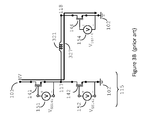
Power switching circuits such as bridge circuits are commonly used in a variety of applications. A prior art circuit schematic of a 3-phase bridge circuit 100 configured to drive a motor is shown in FIG. 1. Each of the three half bridges 115, 125, and 135 in circuit 100 includes two transistors, 141 and 142, 143 and 144, and 145 and 146, respectively, which are able to block voltage in a first direction and are capable of conducting current in the first direction or optionally in both directions. In applications where the transistors employed in the bridge circuit 10 are only capable of conducting current in one direction, for example when the transistors are silicon IGBTs, an anti-parallel diode (not shown) may be connected to each of the transistors 141-146. The gate voltages of each of transistors 141-146 are applied by gate drivers 151-156, respectively. As shown in FIG. 1, gate drivers 151-156 are each coupled between the gate and source of their respective transistor. Gate drivers 151-156 may each be individual circuits. Or, the gate drivers of each half bridge 115, 125, and 135 can be integrated into a single gate drive circuit. Or alternatively, the gate drivers of all of the transistors 141-146 in the bridge circuit can be integrated into a single gate drive circuit.
Each of transistors 141-146 is capable of blocking a voltage at least as large as the high voltage (HV) source 101 of the circuit 100 when they are biased in the OFF state. That is, when the gate-source voltage VGS applied by the gate drive circuits 151-156 to any of transistors 141-146, respectively, is less than the transistor threshold voltage Vth, no substantial current flows through the transistor when the drain-source voltage VDS (i.e., the voltage at the drain relative to the source) is between 0V and HV. When biased in the ON state (i.e. with VGS greater than the transistor threshold voltage), the transistors 141-146 are each capable of conducting sufficiently high current for the application in which they are used.
As used herein, the term “blocking a voltage” refers to a transistor, device, or component being in a state for which significant current, such as current that is greater than 0.001 times the average operating current during regular ON-state conduction, is prevented from flowing through the transistor, device, or component when a voltage is applied across the transistor, device, or component. In other words, while a transistor, device, or component is blocking a voltage that is applied across it, the total current passing through the transistor, device, or component will not be greater than 0.001 times the average operating current during regular ON-state conduction.
The transistors 141-146 may be enhancement mode or E-mode transistors (normally off, Vth>0), or depletion mode or D-mode (normally on, Vth<0) transistors. In power circuits, enhancement mode devices are typically used to prevent accidental turn on which may cause damage to the devices or other circuit components.
Alternatively, the transistors 141-146 can be replaced by a high-voltage D-mode transistor 201 and a low voltage E-mode transistor 202 connected in a cascode configuration 200, as shown in FIG. 2. In prior art cascode device 200 of FIG. 2, the source 211 of D-mode transistor 201 is connected to the drain 216 of E-mode transistor 202, and the gate 212 of D-mode transistor 201 is electrically connected or electrically coupled to the source 214 of E-mode transistor 202. Cascode device 200 is configured to operate as a high-voltage E-mode device, with node 221 functioning as the source, node 222 functioning as the gate, and node 223 functioning as the drain. Referring back to FIG. 1, nodes 117, 118, and 119 are all coupled to one another via inductive loads, i.e., inductive components such as motor coils (not shown in FIG. 1).
As used herein, two or more contacts or other items such as conductive layers or components are said to be “electrically connected” if they are connected by a material which is sufficiently conducting to ensure that the electric potential at each of the contacts or other items is substantially the same or about the same regardless of bias conditions.
FIG. 3A shows prior art half bridge 115 of the full 3-phase motor drive in FIG. 1, along with the winding of the motor (represented by inductive component 321) between nodes 117 and 118. Also shown is transistor 144, into which the motor current feeds. For this phase of power, transistor 144 is continuously ON (Vgs144>Vth) and transistor 142 is continuously OFF (Vgs142<Vth, i.e., Vgs142=0V if enhancement mode transistors are used), while transistor 141 is modulated by gate driver 151 with a pulse width modulation (PWM) signal to achieve the desired motor current. FIG. 3B indicates the path of the current 327 during the time that transistor 141 is biased ON. For this bias, the motor current flows through transistors 141 and 144, while no current flows through transistor 142 because transistor 142 is biased OFF, and the voltage at node 117 is close to HV, so transistor 142 blocks a voltage which is close to HV.
Referring to FIG. 3C, when transistor 141 is switched OFF, no current can flow through transistor 141, so the motor current flows in the reverse direction through transistor 142, which can occur whether transistor 142 is biased ON or OFF. Alternatively, an anti-parallel freewheeling diode (not shown) can be connected across transistor 142, in which case the reverse current flows through the freewheeling diode. During such operation, the inductive component 321 forces the voltage at node 117 to a sufficiently negative value to cause reverse conduction through transistor 142, and transistor 141 blocks a voltage which is close to HV.
The mode of switching illustrated in FIGS. 3A-3C and is commonly known as hard-switching. A hard-switching circuit configuration is one in which the switching transistors are configured to have high currents passing through them as soon as they are switched ON, and to have high voltages across them as soon as they are switched OFF. In other words, the transistors are switched ON during periods where non-zero currents flow through the inductive load, so substantial current flows through the transistors immediately or soon after the transistors are switched ON, rather than the current rising gradually. Similarly, the transistors are switched OFF during periods where high voltages must be blocked by the transistors, so substantial voltage is blocked by the transistors immediately or soon after the transistors are switched OFF, rather than the voltage rising gradually. Transistors switched under these conditions are said to be “hard-switched”.
For the prior art bridge circuits illustrated in FIGS. 1 and 3A-3C, each of the transistors 141-146 has a maximum switching rate at which the device can switch from the OFF state to the ON state or vice-versa, the maximum switching rate being largely dependent on the particular switching characteristics of the device, but also partially depending on other adjacent components in the circuit. The switching time for the switching of the voltages at the output nodes 161-166 of each of the gate drivers 151-156 can be much less than the switching times of each of their respective switching devices 141-146. Consequently, in the configurations of FIGS. 1 and 3A-3C, for which the outputs 161-166 of gate drivers 151-156 are electrically connected directly to the gates of their respective switching devices 141-146, devices 141-146 switch at their maximum switching rates during circuit operation. Furthermore, in order to maintain stability of the devices 141-146 and of the circuit 100, the maximum output current that can be supplied by the gate drivers 151-156 is chosen to be high. For example, the maximum output current of each of the gate drivers 151-156 is typically chosen to be at least 1/60 times the maximum rated output current of each of their respective switching devices 141-146.
Although hard-switched circuits tend to be simple to design and operate, hard-switched components tend to exhibit high levels of electro-magnetic interference (EMI) during operation, in particular in high voltage and/or high current applications in which the switching rate of each of the devices is very high. This can lead to circuit instability or catastrophic failure of the devices in the circuit. In particular, for the circuit configurations shown in FIGS. 1 and 3A-3C, if the circuit high voltage (HV) is large (e.g., greater than 300V) and/or the switching devices need to switch large currents (e.g., greater than 5 Amps), the circuits exhibit excessively high levels of EMI, become unstable, and cease to function properly.
Alternative circuit configurations make use of additional passive and/or active components, or alternatively signal timing techniques, to allow the transistors to be “soft-switched”. A soft-switching circuit configuration is one in which the switching transistors are configured to be switched ON during zero-current (or near zero-current) conditions and switched OFF during zero-voltage (or near zero-voltage) conditions. Soft-switching methods and configurations have been developed to address the high levels of EMI and associated ringing observed in hard-switched circuits, especially in high current and/or high voltage applications. While soft-switching can in many cases alleviate these problems, the circuitry required for soft switching typically includes many additional components, resulting in increased overall cost and complexity. Soft-switching also typically requires that the circuits be configured to switch only at specific times when the zero-current or zero-voltage conditions are met, hence limiting the control signals that can be applied and in many cases reducing circuit performance. Hence, alternative configurations and methods are desirable for power switching circuits in order to maintain sufficiently low levels of EMI while at the same time maintaining circuit stability.
SUMMARY
Described herein are high-voltage circuits which include high-voltage switching devices. The gate drivers of the switching devices are configured to reduce the switching rates of the switching devices during operation and improve stability of the high-voltage circuits.
In a first aspect, an electronic component includes a switching device comprising a source, a gate, and a drain, the switching device having a predetermined device switching rate. The electronic component further includes a gate driver electrically connected to the gate and coupled between the source and the gate of the switching device, the gate driver configured to switch a gate voltage of the switching device at a gate driver switching rate. The gate driver is configured such that in operation, an output current of the gate driver cannot exceed a first current level, wherein the first current level is sufficiently small to provide a switching rate of the switching device in operation to be less than the predetermined device switching rate.
In a second aspect, an electronic component includes a switching device comprising a source, a gate, and a drain, the switching device being operable to block at least 300V when biased OFF. The electronic component further includes a gate driver coupled between the source and the gate of the switching device, the gate driver configured to switch voltage at an output of the gate driver at a gate driver switching rate. A resistance between the output of the gate driver and the gate of the switching device is less than 5 Ohms, and the gate driver is configured such that in operation, an output current of the gate driver is limited by circuitry of the gate driver such that the output current cannot exceed a first current level. Furthermore, a ratio of the first current level to a maximum rated current of the switching device is less than 1/100.
In a third aspect, a method of operating an electronic component is described. The electronic component includes a switching device comprising a source, a gate, and a drain, the switching device configured to have a predetermined device current switching rate. The electronic component also includes a gate driver coupled between the source and the gate of the switching device. The method includes causing the gate driver to switch an output voltage of the gate driver from a first state to a second state at a gate driver switching rate, whereby a gate voltage of the switching device is switched at substantially the same rate as the gate driver switching rate, and wherein switching of the output voltage of the gate driver from the first state to the second state causes current through the switching device to be switched at a current switching rate less than the predetermined device current switching rate.
In a fourth aspect, a circuit includes a switching device having a maximum rated current and comprising a source, a gate, and a drain. The circuit also includes a first voltage supply which applies an output voltage of at least 300 Volts, and a gate driver connected to a second voltage supply and coupled between the source and the gate of the switching device, the gate driver configured to switch a gate voltage of the switching device at a gate driver switching rate. The gate driver is configured such that in operation, an output current of the gate driver cannot exceed a first current level. Furthermore, the switching device is configured to block the output voltage applied by the first voltage supply during at least a portion of operation of the circuit, a ratio of the first current level to the maximum rated current of the switching device is less than 1/100, and in operation of the circuit, a voltage switching rate of the switching device is greater than 100 Volts/nanosecond.
The electronic components, circuits, and methods described herein can include one or more of the following features. The electronic component can be part of a half bridge circuit. The switching device can comprise a III-Nitride transistor. The switching device can comprise an enhancement-mode transistor coupled to a depletion-mode transistor. The depletion-mode transistor and the enhancement-mode transistor can be configured such that a source of the enhancement-mode transistor serves as the source of the switching device, a gate of the enhancement-mode transistor serves as the gate of the switching device, and a drain of the depletion-mode transistor serves as a gate of the switching device. The switching device can be operable to block at least 300V when biased OFF. A maximum rated current of the switching device can be at least 50 Amps. A ratio of the first current level to a maximum rated current of the switching device can be less than 1/100. The switching rate of the switching device in operation can be less than 0.5 times the predetermined device switching rate. The output of the gate driver can be directly connected to the gate of the switching device. The electronic component or circuit can further include a ferrite bead connected between the output of the gate driver and the gate of the switching device.
An output of the gate driver can be electrically connected to the gate, and switching the output voltage of the gate driver from the first state to the second state can cause a voltage of at least 300V to be switched across the switching device. A maximum output current of the gate driver can be sufficiently small to cause the current switching rate of the switching device to be less than the predetermined device current switching rate. The circuit can be a half bridge. The half bridge can be connected to an inductive load, wherein in operation, a current greater than 1 Amp passes through the inductive load. The second voltage supply can apply an output voltage that is substantially less than the output voltage of the first voltage supply. The second voltage supply can apply an output voltage less than 25 Volts. An output of the gate driver can be electrically connected to the gate of the switching device. The circuit can further comprise a resistor between an output of the gate driver and the gate of the switching device, wherein the resistor has a resistance between 0 Ohms and 5 Ohms. The switching device can comprise a III-Nitride transistor.
The details of one or more embodiments of the subject matter described in this specification are set forth in the accompanying drawings and the description below. Other features, aspects, and advantages of the subject matter will become apparent from the description, the drawings, and the claims.
DESCRIPTION OF DRAWINGS
FIG. 1 illustrates a circuit schematic of a prior art 3-phase bridge circuit.
FIG. 2 is a prior art circuit schematic of two transistors arranged in a cascode configuration.
FIGS. 3A-3C illustrate portions of the prior art 3-phase bridge circuit of FIG. 1 under various operating conditions.
FIGS. 4-5 illustrate half bridge circuits configured to drive electrical loads.
FIG. 6 is a cross-sectional schematic view of a III-Nitride enhancement-mode transistor.
FIGS. 7-8 illustrate half bridge circuits configured to drive electrical loads.
FIG. 9 is a circuit schematic of a cascode device that can be used as a switching device in the half bridge circuit of FIG. 8.
FIG. 10 is a cross-sectional schematic view of a III-Nitride depletion-mode transistor.
FIGS. 11 and 12 are illustrations of bidirectional switches.
FIG. 13 is a plot of voltage and current characteristics as a function of time for a switching device of the half bridge circuit of FIG. 8 during circuit operation.
Like reference symbols in the various drawings indicate like elements.
DETAILED DESCRIPTION
Described herein are configurations and methods for slowing the switching rate (i.e., the slew rate) of switching devices utilized in electronic components and circuits. This reduction in switching rate reduces levels of EMI in the circuits during and immediately following switching, thereby allowing for improved circuit stability, in particular in applications where high currents (e.g., 4 Amps or higher) and/or high voltages (e.g., greater than 300V) are being switched by the switching devices.
Each of the transistors or other switching devices in the circuits and components described herein can be configured to be hard-switched, as previously described, at a particular switching rate. When a transistor of one of the circuits herein is in the OFF state with no substantial current flowing through it, it supports a large voltage which can be about equal to or close to the circuit high voltage. When a transistor of one of the circuits herein is in the ON state, it typically has substantial current passing through it with only a small voltage across it. The switching time of a switching transistor switched under hard-switching conditions is defined as follows. When the transistor is switched from the OFF state described above to the ON state described above, the current through the device begins to increase at the onset of switching, while the voltage across the device remains approximately the same. The voltage across the device does not begin to drop substantially until the point at which substantially all the load current passes through the transistor. The time that elapses between the onset of switching and the point at which the voltage begins to drop is referred to as the “delay time” of the device. This is also the time that is required for the output of the device to begin to respond to a signal applied to the input. After the delay time is reached, the voltage across the transistor begins to drop. The time that elapses from the onset of this voltage drop to the point at which the voltage reaches its steady-state value is referred to as the “transition time” of the device. The time that elapses between the onset of switching and the point at which the voltage across the device drops to its steady-state value, which is the sum of the delay time and the transition time, is referred to as the “switching time” for turning the transistor on. The total current switched divided by the delay time, (dI/dt), is referred to as the “current switching rate”. The total voltage switched across the device divided by the transition time, (dV/dt), is referred to as the “voltage switching rate”. In general, while shorter switching times (and therefore faster switching rates) typically result in lower switching losses, they typically also cause higher levels of EMI, which can degrade circuit components or damage them such that they may be rendered inoperable. Reducing the current and/or voltage switching rates of the switching devices during circuit operation can mitigate these deleterious effects.
An implementation of a power conversion circuit in which the switching rate of the switching devices is reduced is illustrated in FIG. 4. As seen in FIG. 4, half bridge 415 includes high side switching device 441 and low side switching device 442. Switching devices 441 and 442 are implemented as silicon-based power MOSFETs (metal-oxide-semiconductor field-effect transistors) or IGBTs (insulated gate bipolar transistors). Because MOSFETs and IGBTs have inherent low-performance anti-parallel diodes integrated into their device structures, external diodes 481 and 482 are connected anti-parallel to switches 441 and 442, respectively, in order to minimize losses during times where the switches carry reverse freewheeling currents. The output node 417 of the half bridge 415 is connected to a load 421.
The gates of switching devices 441 and 442 are switched by gate drivers 451 and 452, respectively. The voltages applied at the outputs of the gate drivers are provided by power supplies (e.g., voltage supplies) 491 and 492, which are connected to each of the gate drivers 451 and 452. Each gate driver is configured to apply this voltage at its output when the switching device is to be turned ON, and to remove this voltage (i.e., to apply 0 Volts) when the switching device is to be turned OFF. The voltages provided by voltage supplies 491 and 492 are typically much smaller than the circuit high voltage (HV) 401, which is provided by a different power supply. For example, in high voltage applications where the circuit high voltage 401 is greater than 300 Volts, voltage supplies 491 and 492 typically provide a voltage of about 25 Volts or less, for example about 12 Volts.
The switching time that elapses while gate drivers 451 and 452 switch the voltages at their respective outputs 461 and 462 can be much less than the minimum switching time of switching devices 441 and 442. As shown in FIG. 4, resistors 471 and 472 are inserted between the gates of switching devices 441 and 442, respectively, and the outputs 461 and 462 of their respective gate drivers 451 and 452. This causes the voltage at the gates of switching devices 441 and 442 to vary more slowly than at the outputs 461 and 462 of their respective gate drivers 451 and 452, thereby slowing the switching rate of each of switches 441 and 442 to a value lower than their maximum switching rates. In high voltage applications, for example applications in which the circuit high voltage (HV) 401 is at least 300V, because the gate charge of an IGBT or a MOSFET is large, a small resistor can be used for each of resistors 471 and 472 in order to achieve the desired reduction in switching rate. For example, in the case where switching devices 441 and 442 are rated to support a maximum current of 60 amps or larger and an OFF state voltage of at least 300V, resistors 471 and 472 can each have a resistance that is substantially less than 40 ohms but greater than 8 ohms, for example between 10 and 20 ohms. However, in these high voltage applications (i.e., where the circuit high voltage supply is greater than 300V), the switching devices 441 and 442, which are IGBTs/MOSFETs, become unstable if a gate resistor 471/472 is not included between the gate driver and the gate of the switching device, or if the gate resistor is too small (e.g., less than about 7-8 ohms).
During switching of devices 441 and 442, current flows through the outputs 461 and 462 of gate drivers 451 and 452 onto the gates of devices 441 and 442. In many cases, for MOSFET or IGBT switching devices, in order to maintain circuit stability, in addition to inclusion of resistors 471 and 472, the gate drivers must be capable of providing adequate output currents, the amount of current needed being proportional to the gate width, and hence to the current handling capabilities of the switching device (since the current handling capabilities are also proportional to the gate width). Thus, the maximum output current of the gate drivers must be kept above a minimum value, the minimum value being proportional to the current handling capabilities and the gate width of their respective switching devices. For example, for a MOSFET or IGBT with a maximum rated current of 60 Amps and an OFF state operating voltage of at least 300V, the gate driver must have a maximum output current of at least 1.4 Amps and resistors 471 and 472 have at least about 10 ohms of resistance in order to prevent instability in the circuit. More generally, the ratio of maximum output current of the gate driver to maximum rated current of the switching device must be at least 1.4/60, and is typically much higher. This condition typically must be maintained when a resistor is connected between the gate driver and the gate of the switching device in order to reduce the device switching rate, as in FIG. 4, and also when the resistor is omitted and the output of the gate driver is electrically connected directly to the gate of the switching device, as was shown in FIGS. 1 and 3A-3C. If this condition is not maintained, in particular in applications where the switching devices block at least 300V when they are biased in the OFF state, the circuit can become unstable during operation. Hence, in the half bridge circuit of FIG. 4, gate drivers 451 and 452 are both configured to supply maximum output currents that are at least 1.4/60 times the maximum rated currents of switches 441 and 442.
In some high voltage applications (i.e., half bridges where the high voltage is greater than 300V) in which the load currents are very high, for example 300 Amps or higher, the ratio of the maximum output current of the gate driver 451 or 452 to the maximum rated current of the IGBT or MOSFET switching device 441 or 442 may be less than 1/60. In these applications, if the outputs 461/462 of gate drivers 451/452, respectively, were connected directly to the gates of the IGBT/MOSFET switching devices, the half bridge 415 would be unstable and would not function properly. Hence, in applications that require such high currents, resistors 471 and 472 are required for proper operation of half bridge 415, and each of the resistors needs to have a resistance of at least about 10 ohms.
The maximum rated current of a transistor or other switching device is defined as follows. When the gate of the switching device is biased relative to the source at a voltage slightly higher than the device threshold voltage, the device is in the ON state, and current flows from the drain to the source when a small drain-source voltage (i.e., a drain-source voltage that is much smaller than the device breakdown voltage but greater than the device knee voltage) is applied. If the gate voltage is increased, the current increases up to a maximum value and then ceases to increase even if the gate voltage is further increased. This maximum value is larger if the current is only applied in short enough pulses (e.g., about 1 microsecond or less) that the device does not substantially heat up. This maximum value under short current pulse conditions is the maximum rated current of the switching device.
FIG. 5 illustrates another half bridge circuit 515 in which III- Nitride transistors 541 and 542, which for example can be III-Nitride high electron mobility transistors (HEMTs), are implemented as the high side and low side switch, respectively. III- Nitride transistors 541 and 542 have the same maximum current rating and voltage handling characteristics as devices 441 and 442 of FIG. 4. Because the III-Nitride transistors are capable of flowing reverse freewheeling currents through their channels, even when their gates are biased OFF relative to their sources, freewheeling diodes such as diodes 481 and 482 shown in FIG. 4 are not required, although they may optionally be included.
III-Nitride transistors are desirable for many of the applications in which high-voltage and/or high-current switching is required, due to their ability to incur minimal switching losses when they are hard-switched at high switching rates. However, because these devices inherently have very high predetermined switching rates (much higher than silicon-based MOSFETs and IGBTs), it is often desirable to reduce the switching rate during operation in order to minimize EMI and associated instabilities. As used herein, the terms III-Nitride or III-N materials, layers, devices, structures, etc., refer to a material, layer, device, or structure comprised of a compound semiconductor material according to the stoichiometric formula BwAlxInyGazN, where w+x+y+z is about 1, 0≦w≦1, 0≦x≦1, 0≦y≦1, and 0≦z≦1. In a III-Nitride or III-N device, such as a transistor or HEMT, the conductive channel can be partially or entirely contained within a III-N material layer.
An example of a III-N HEMT device 60 that can be implemented for switching devices 541 and 542 of FIG. 5 is shown in FIG. 6. Referring to FIG. 6, device 60 is an enhancement-mode III-Nitride transistor. Device 60 includes a substrate 10 (although the substrate is optional), which can for example be silicon, and a III-Nitride material structure on the substrate, the III-Nitride material structure including a III-N channel layer 11, which can for example be GaN, and a III-N barrier layer 12, which can for example be AlGaN. A two-dimensional electron gas (2DEG) channel 19 is induced in the III-N channel layer 11 adjacent to the III-N barrier layer 12 due to a compositional difference between the III-N channel and barrier layers. Source contact 74 and drain contact 75 are on opposite sides of gate 88 and electrically contact the 2DEG channel 19. Gate 88 is formed over a gate insulator layer 87, and both layers 87 and 88 are in a recess that extends into the III-Nitride material structure. An insulating material structure which includes an insulating layer 22, an etch stop layer 21, and an electrode defining layer 33 is formed over the III-N material structure, and a recess 17 is formed in the insulating material structure. A source-connected field plate 71 extends from the source towards the gate, and a portion of field plate 71 is in the recess 17.
As seen in FIG. 6, device 60 is a lateral device. That is, the transistor channel is contained within a semiconductor layer 11 of the transistor 60, and the source, gate, and drain electrodes 74, 88, and 75, respectively, are on the same side of the semiconductor layer 11, as shown. Specifically, the portions of the source and drain electrodes 74 and 75 that form an ohmic contact to the channel in layer 11, as well as the portion of the gate electrode 88 that modulates the current in the channel, are each on the same side of the semiconductor layer 11.
Referring back to FIG. 5, the output node 417 of the half bridge 515 is connected to a load 421. Half bridge 515 also uses the same gate drivers 451 and 452 and corresponding voltage supplies 491 and 492 as those used in the circuit of FIG. 4 to drive the gates of transistors 541 and 542. Resistors 571 and 572 are inserted between the gates of switching devices 541 and 542, respectively, and the outputs 461 and 462 of their respective gate drivers 451 and 452, in order to reduce the switching rate of each of switches 541 and 542 to a value lower than their maximum switching rates. However, because the gate charge of a III-Nitride transistor, and in particular a lateral III-Nitride transistor, is much less than that of an IGBT or MOSFET of the same maximum current rating and voltage handling characteristics, resistors 571 and 572 need to be made substantially larger than resistors 471 and 472 of FIG. 4 in order to sufficiently reduce the switching rate of transistors 541 and 542. For example, in the case where switching devices 541 and 542 are rated to support a maximum current of 60 amps and an OFF state voltage of at least 300V, resistors 471 and 472 can each have a resistance that is at least 50 ohms in order to effectively reduce the switching rate of transistors 541 and 542. However, current noise (from thermal currents and/or other noise sources) Inoise that passes through resistors 571 and 572 creates voltage noise (e.g., voltage fluctuations) Vnoise at the gates of transistors 541 and 542. These voltage fluctuations Vnoise are given by the equation Vnoise=Inoise*R, where R is the resistance of resistors 571 and 572. Hence if R is made large, as is required in the circuit of FIG. 5 to effectively reduce the switching rate of transistors 541 and 542 during operation, Vnoise becomes large, which results in the circuit being unstable. Hence in some applications, when devices with low gate charge, such as III-Nitride transistors, are used as high-current/high-voltage switches, the switching rate of the switches cannot be reduced by adding a resistor between the transistor and the gate driver without making the circuit unstable.
FIG. 7 illustrates a half bridge circuit 715 which is similar to half bridge circuit 515 of FIG. 5, and uses the same switching transistors 541 and 542, but resistors 571 and 572 have been omitted. Furthermore, gate drivers 451 and 452 and corresponding power supplies 491 and 492 of circuit 515 of FIG. 5 have been replaced by gate drivers 751 and 752 and corresponding power supplies 791 and 792, which have specific properties that cause the current and/or voltage switching rates of transistors 541 and 542 to be reduced without the need for an intermediary gate resistor, as described in more detail below. The outputs 761 and 762 of gate drivers 751 and 752, respectively, are electrically connected (i.e., directly connected) to the gates of switching devices 541 and 542.
The voltage supplies 791 and 792 that are connected to gate drivers 751 and 752, respectively, have similar voltage output characteristics to voltage supplies 491 and 492 of FIGS. 4-5. However, gate drivers 751 and 752 of half bridge circuit 715 are configured to have a much lower limit on their maximum rated output currents (i.e., the maximum output current that they are able to supply or sink during operation), as compared to the gate drivers 451 and 452 of half bridges 415 (in FIG. 4) and 515 (in FIG. 5). Specifically, the circuitry of the gate driver can be configured to limit the output current of the gate driver such that it cannot exceed a predetermined value during operation. It has been found that for high voltage switching devices that inherently exhibit very low minimum switching times (and therefore high maximum switching rates) and in which the gate charge is low (which is the case with III-Nitride switching transistors), using a gate driver with a low maximum rated output current reduces the current switching rate of the transistor during operation (and in some cases also the voltage switching rate) without the need for a resistor between its gate and the output node of the gate driver. Furthermore, such a configuration has been found to substantially improve circuit stability. Alternatively, although not shown in FIG. 7, a small resistor, having a resistance between 0 and 5 Ohms, could be included between the outputs of the gate drivers and the gates of the transistors, and the resulting circuit would still exhibit the advantages described above. In another alternative configuration, also not shown in FIG. 7, a ferrite bead is included between the outputs of one or more of the gate drivers and the gates of their associated transistors.
As an example, for a half bridge 715 of FIG. 7 utilizing III- Nitride transistors 541 and 542 configured to block at least 300V in the OFF state and rated to support a maximum current of 60 Amps in the ON state, in the case where the resistance between the output of the outputs of the gate drivers and the gates of their associated transistors is 0 Ohms or between 0 and 5 Ohms, employing gate drivers 751 and 752 with maximum output currents of less than 1 Amp, for example about 0.5 Amps or less, causes a substantial reduction in the current switching rate of the III-Nitride transistors during operation, hence increasing the switching time, and at the same time improves the stability of the circuit. In general, employing gate drivers for which the ratio of the maximum output current of the gate driver to the maximum rated current of the III-Nitride transistors is less than 1/60, for example less than 1/100, or less than 1/150, reduces the switching rate of the III-Nitride transistors during operation while at the same time improving the stability of the circuit. These advantages are realized both when the outputs of the gate drivers are directly connected to the gates of their associated transistors, and when a small resistor having a resistance between 0 and 5 Ohms is inserted between the outputs of the gate drivers and the gates of their associated transistors. These advantages are also realized when a ferrite bead is inserted between the outputs of one or more of the gate drivers and the gates of their associated transistors.
The above results were unexpected for several reasons. First, it was not obvious that utilizing a gate driver with a reduced maximum output current would reduce the switching rate of the III-Nitride transistors during operation. Second, it was not expected that such a configuration would substantially improve the stability of the circuit, in particular because when such a low output current gate driver configuration is employed using different switching devices, such as silicon MOSFETs and IGBTs, in the same applications, in particular without a sufficiently large gate resistor (e.g., 10 Ohms or larger), the circuits in fact become unstable.
While in FIG. 7, switching devices 541 and 542 are each shown to be a single transistor, other devices could be used, provided that they have characteristics that allow their switching rates to be reduced by employing a gate driver with a low maximum current, and they do not become unstable or cause the circuit to become unstable when such a configuration is implemented. For example, a high-voltage hybrid enhancement-mode device 900, shown in FIG. 9, could be used in place of each of transistors 541 and 542 in the half bridge 715 of FIG. 7. Such a configuration is shown in FIG. 8, which illustrates another half bridge 815 that is the same as half bridge 715 of FIG. 7, except that the high-side and low- side switches 841 and 842, respectively, are each implemented as a high-voltage hybrid enhancement-mode device 900, shown in FIG. 9.
As used herein, a “high-voltage switching device”, such as a high-voltage switching transistor, is an electronic device which is optimized for high-voltage switching applications. That is, when the transistor is off, it is capable of blocking high voltages, such as about 300V or higher, about 600V or higher, about 1200V or higher, or about 1700V or higher, and when the transistor is on, it has a sufficiently low on-resistance (RoN) for the application in which it is used, i.e., it experiences sufficiently low conduction loss when a substantial current passes through the device. A high-voltage device can at least be capable of blocking a voltage equal to the high-voltage supply or the maximum voltage in the circuit for which it is used. A high-voltage device may be capable of blocking 300V, 600V, 1200V, 1700V, or other suitable blocking voltage required by the application. In other words, a high-voltage device can block any voltage between 0V and at least Vmax, where Vmax is the maximum voltage that could be supplied by the circuit or power supply. In some implementations, a high-voltage device can block any voltage between 0V and at least 2*Vmax. As used herein, a “low-voltage device”, such as a low-voltage transistor, is an electronic device which is capable of blocking low voltages, such as between 0V and Vlow (where Vlow is less than Vmax), but is not capable of blocking voltages higher than Vlow. In some implementations, Vlow is equal to about |Vth|, greater than |Vth|, about 2*|Vth|, about 3*|Vth|, or between about |Vth| and 3*|Vth|, where |Vth| is the absolute value of the threshold voltage of a high-voltage transistor, such as a high-voltage-depletion mode transistor, contained within a hybrid component, such as that illustrated in FIGS. 7a and 7b and described in further detail below. In other implementations, Vlow is about 10V, about 20V, about 30V, about 40V, or between about 5V and 50V, such as between about 10V and 40V. In yet other implementations, Vlow is less than about 0.5*Vmax, less than about 0.3*Vmax, less than about 0.1*Vmax, less than about 0.05*Vmax, or less than about 0.02*Vmax.
Referring to FIG. 9, since high-voltage III-N enhancement-mode transistors can be difficult to fabricate reliably, one alternative to a single high-voltage III-N E-mode transistor is to combine a high-voltage III-N D-mode transistor 901 with a low-voltage E-mode transistor 902 in the configuration of FIG. 9 to form a hybrid device 900. Hybrid device 900 can be operated in the same way as a single high-voltage E-mode transistor, and in many cases achieves the same or similar output characteristics as a single high-voltage E-mode transistor. Hybrid device 900 includes a high-voltage III-N D-mode transistor 901 and a low-voltage E-mode transistor 902, which can for example be a low-voltage silicon power MOSFET. E-mode transistor 902 can be a vertical transistor, having its drain electrode 916 on the opposite side of the device semiconductor layers from its source electrode 914 and gate electrode 915, and D-mode III-N transistor 901 can be a lateral transistor, having its source electrode 911, gate electrode 912, and drain electrode 913 all on the same side of the device III-N layers. However, other configurations for each of transistors 901 and 902 are possible as well.
FIG. 10 illustrates an example III-N D-mode transistor 1000 that could be used for transistor 901 in FIG. 9. Transistor 1000 includes a substrate 1010 (although the substrate is optional), which can for example be silicon, and a III-Nitride material structure on the substrate, the III-Nitride material structure including a III-N channel layer 1011, which can for example be GaN, and a III-N barrier layer 1012, which can for example be AlGaN. A two-dimensional electron gas (2DEG) channel 1019 is induced in the III-N channel layer 1011 adjacent to the III-N barrier layer 1012 due to a compositional difference between the III-N channel and barrier layers. Source contact 1014 and drain contact 1015 are on opposite sides of electrode 1029 and electrically contact the 2DEG channel 19. Electrode 1029 includes the device gate 1016, as well as a field plate portion 1024 which extends from the gate 1016 towards the drain contact 1015. Electrode-defining layer 1023 is formed of an insulating material. A gate dielectric (not shown) may optionally be included between the gate 1016 and the underlying III-N material layers.
As seen in FIG. 10, transistor 1000 is a lateral device. That is, the transistor channel is contained within a semiconductor layer 1011 of the transistor 1000, and the source, gate, and drain electrodes 1014, 1016, and 1015, respectively, are on the same side of the semiconductor layer 1011. Specifically, the portions of the source and drain electrodes 1014 and 1015 that form an ohmic contact to the channel in layer 1011, as well as the portion of the gate 1016 that modulates the current in the channel, are each on the same side of the semiconductor layer 1011.
Referring back to FIG. 9, the source electrode 914 of the low-voltage E-mode transistor 902 and the gate electrode 912 of the high-voltage D-mode transistor 901 are electrically connected together, for example with wire bonds or other metal interconnections if they are integrated into a single structure, and together form the source 921 of the hybrid device 900. The gate electrode 915 of the low-voltage E-mode transistor 902 functions as the gate 922 of the hybrid device 900. The drain electrode 913 of the high-voltage D-mode transistor 901 functions as the drain 923 of the hybrid device 900. The source electrode 911 of the high-voltage D-mode transistor 901 is electrically connected to the drain electrode 916 of the low-voltage E-mode transistor 902.
As used herein, a “hybrid enhancement-mode electronic device or component”, or simply a “hybrid device or component”, is an electronic device or component formed of a depletion-mode transistor and a enhancement-mode transistor, where the depletion-mode transistor is capable of a higher operating and/or breakdown voltage as compared to the enhancement-mode transistor, and the hybrid device or component is configured to operate similarly to a single enhancement-mode transistor with a breakdown and/or operating voltage about as high as that of the depletion-mode transistor. That is, a hybrid enhancement-mode device or component includes at least 3 nodes having the following properties. When the first node (source node) and second node (gate node) are held at the same voltage, the hybrid enhancement-mode device or component can block a positive high voltage (i.e., a voltage larger than the maximum voltage that the enhancement-mode transistor is capable of blocking) applied to the third node (drain node) relative to the source node. When the gate node is held at a sufficiently positive voltage (i.e., greater than the threshold voltage of the enhancement-mode transistor) relative to the source node, current passes from the source node to the drain node or from the drain node to the source node when a sufficiently positive voltage is applied to the drain node relative to the source node. When the enhancement-mode transistor is a low-voltage device and the depletion-mode transistor is a high-voltage device, the hybrid component can operate similarly to a single high-voltage enhancement-mode transistor. The depletion-mode transistor can have a breakdown and/or maximum operating voltage that is at least two times, at least three times, at least five times, at least ten times, or at least twenty times that of the enhancement-mode transistor.
It has been found that when a hybrid device such as device 900 shown in FIG. 9 is used for switching devices 841 and 842 in half bridge 815 of FIG. 8, utilizing gate drivers 751 and 752 with low maximum output currents provides the same reduction in switching speed and improvements in circuit stability that were previously described for half bridge 715 of FIG. 7. Specifically, for a half bridge 815 utilizing hybrid device 900 of FIG. 9 for switches 841 and 842, where each of the switches is configured to block at least 300V in the OFF state and rated to support a maximum current of 60 Amps in the ON state, employing gate drivers 751 and 752 with maximum rated output currents of less than 1 Amp, for example about 0.5 Amps or less, causes a substantial reduction in the current switching rate of the hybrid devices during operation, and at the same time improves the stability of the circuit. This effect was also observed to occur when a small resistor (having a resistance between 0 and 5 Ohms) or a ferrite bead was inserted between the outputs of one or more of the gate drivers and the gates of their associated transistors. This result was unexpected for the same reasons provided above with reference to half bridge 715 of FIG. 7. Furthermore, gate drivers with even lower output currents may additionally reduce the voltage switching rate of the hybrid devices during operation, thereby providing added stability.
As described above, for half bridge 815 of FIG. 8, employing gate drivers 751 and 752 with maximum output currents of less than 1 Amp causes a substantial reduction in the current switching rate of the hybrid devices during operation and at the same time improves the stability of the circuit. However, even when a gate driver with a maximum rated current level as low as 0.5 Amps is used, the voltage switching rate remains greater than 100 Volts/nanosecond. High voltage switching rates are desirable in many applications because they can reduce switching losses during operation. However, stable operation with such high device voltage switching rates typically cannot be achieved in conventional half bridge circuits. Hence, use of gate drivers 751 and 752, in which the maximum current level that the gate driver is capable of providing at its output is less than 1/100 times the maximum rated current of the switching devices 841 and 842, allows for stable operation of the circuit, even with device voltage switching rates greater than 100 Volts/nanosecond. This result is unexpected for the same reasons previously provided.
FIG. 13 is a plot of the current and voltage characteristics of high side switching device 841 of FIG. 8 during a switching sequence in the case where the circuit high voltage 401 was maintained at 450 Volts, such that a voltage greater than 400 Volts, and substantially greater than 300 Volts, was switched across switching device 841. Gate drivers 751 and 752 were each configured such that the maximum current they were able to provide through their respective outputs was 0.5 Amps. Low side switching device 842 was kept OFF, while high side switching device 841 was switched, such that the mode of operation (in terms of the path that the current flowed) was similar to that shown for half bridge 115 in FIGS. 3B-3C. Switching devices 841 and 842 each had a maximum rated current level of 60 Amps, and were configured to be capable of blocking 600V. Curve 1320 is a plot of the voltage at node 417 as a function of time, and curve 1340 is a plot of the current passing through the load 421 as a function of time. The axis on the left hand side of the plot corresponds to curve 1320, and the axis on the right hand side of the curve corresponds to curve 1340. The voltage switching rate of switching device 841 during operation was greater than 100 Volts/nanosecond. The voltage switched across the device 841 is indicated by arrow 1322.
As seen in FIG. 13, immediately after switching device 841 is switched ON or OFF, the voltage across the device oscillates but eventually stabilizes. For example, voltage oscillations 1324 occur after the second time during the switching sequence that switching device 841 is switched ON. The voltage overshoot above the desired voltage level that results from oscillations 1324 is indicated by arrow 1326. As seen, during each switching cycle when the switching device 841 is switched ON, the voltage overshoot remains less than 20% of the circuit high voltage (i.e., the approximate voltage switched across the switching device), even when the current switched through the switching device 841 is greater than 2 Amps. That is, the maximum voltage across switching device 841 was at all times less than 1.3 times and also less than 1.2 times the circuit high voltage during operation of the half bridge. Because the voltage across switching device 841 at all times remained less than 1.5 times the circuit high voltage, the voltage blocking capabilities of the switching devices 841 and 842 did not need to be overspecified as highly as would be required in typical high voltage circuits, allowing for a wider range of operating voltages for the half bridge circuit. Similar low-noise operation was also obtained when the high side switching device 841 was continuously biased OFF and the low side switching device 842 was switched. Such a low voltage overshoot at such high switching rates resulted from the use of gate drivers 751 and 752 with low maximum output current levels. For comparison, when the gate drivers 751 and 752 were replaced with gate drivers for which the output current was limited to 4 Amps and the same switching sequence shown in FIG. 13 was applied, the voltage overshoots were so large that the switching devices broke down and the circuit was rendered inoperable before the completion of a single switching sequence.
In typical power switching applications in which high-voltage switching devices are used, the device is, during the majority of time, in one of two states. In the first state, which is commonly referred to as the “on state”, the voltage at the gate electrode relative to the source electrode is higher than the device threshold voltage, and substantial current flows through the device. In this state, the voltage difference between the source and drain is typically low, usually no more than a few volts, such as about 0.1-5 volts. In the second state, which is commonly referred to as the “off state”, the voltage at the gate electrode relative to the source electrode is lower than the device threshold voltage, and no substantial current, apart from off-state leakage current, flows through the device. In this second state, the voltage between the source and drain can range anywhere from about 0V to the value of the circuit high voltage supply, which in some cases can be as high as 100V, 300V, 600V, 1200V, 1700V, or higher, but can be less than the breakdown voltage of the device. In some applications, inductive elements in the circuit cause the voltage between the source and drain to be even higher than the circuit high voltage supply. Additionally, there are short times immediately after the gate has been switched on or off during which the device is in a transition mode between the two states described above. When the device is in the off state, it is said to be “blocking a voltage” between the source and drain. As used herein, “blocking a voltage” refers to the ability of a transistor, device, or component to prevent significant current, such as current that is greater than 0.001 times the average operating current during regular on-state conduction, from flowing through the transistor, device, or component when a voltage is applied across the transistor, device, or component. In other words, while a transistor, device, or component is blocking a voltage that is applied across it, the total current passing through the transistor, device, or component will not be greater than 0.001 times the average operating current during regular on-state conduction.
While the configurations and methods for reducing switching rates of transistors while improving circuit stability were described here with reference to bridge circuits and half bridges, the same methods and configurations can be used to achieve the same results in other circuits, for example power factor correction (PFC) circuits or AC-AC conversion circuits such as matrix converters. Additionally, in some applications, other types of switching devices may be utilized. For example, in an AC-AC converter, the switching devices can each be bidirectional switches, such as a III-N bidirectional switch 1100 (shown in FIG. 11) or a hybrid III-N bidirectional switch 1200 (as shown in FIG. 12).
As seen in FIG. 11, III-N bidirectional switch 1100 includes substrate 10, as well as III-N layers 11 and 12, in which the device 2DEG channel 19 is contained. Switch 1100 also includes power electrodes 1124 and 1134, which contact the channel 19 and both function as device sources and drains, depending on the direction of current flow or on the voltage polarity across the device. Gates 1128 and 1138 are between power electrodes 1124 and 1134, and are configured similarly to gate 88 of the enhancement-mode transistor 60 shown in FIG. 6. Although not shown in FIG. 11, device 1100 is configured to be operated with two gate drivers. A first gate driver is connected between gate 1128 and power electrode 1124, and a second gate driver is connected between gate 1138 and power electrode 1134. Each gate driver can be similar to or the same as gate drivers 791 and 792 of FIGS. 7 and 8. That is, in order to reduce the switching rate of switch 1100 and provide for stable operation of the circuit in which switch 1100 is used, the maximum current that each gate driver is capable of providing can be less than 1/100 times the maximum rated current of the bidirectional switch 1100.
Referring to FIG. 12, bidirectional switch 1200 includes a high voltage depletion-mode III-N bidirectional switch 1210 connected in a cascode configuration to low voltage enhancement- mode transistors 1261 and 1262 to form a high voltage enhancement-mode bidirectional switch 1200. Power electrode 1224 of the III-N bidirectional switch 1210 is connected to the drain of transistor 1261. Power electrode 1234 of the III-N bidirectional switch 1210 is connected to the drain of transistor 1262. Gate electrode 1228 of the III-N bidirectional switch 1210 is connected to the source of transistor 1261. Gate electrode 1238 of the III-N bidirectional switch 1210 is connected to the source of transistor 1262. Anti-parallel diodes 1271 and 1272 are optionally provided across transistors 1261 and 1262, respectively. Gate driver 1251 is coupled between the gate and source of transistor 1261. Gate driver 1252 is coupled between the gate and source of transistor 1262. Each gate driver 1251 and 1252 can be similar to or the same as gate drivers 791 and 792 of FIGS. 7 and 8. That is, in order to reduce the switching rate of switch 1200 and provide for stable operation of the circuit in which switch 1200 is used, the maximum current that each gate driver is capable of providing can be less than 1/100 times the maximum rated current of the bidirectional switch 1200.
A number of implementations have been described. Nevertheless, it will be understood that various modifications may be made without departing from the spirit and scope of the techniques and devices described herein. For example, in the circuits of FIGS. 7 and 8, a small resistor (with resistance between 0 and 5 Ohms) could be inserted between each gate driver and the gate of its corresponding switching device. In high voltage applications, when MOSFETs or IGBTs are used for the switching devices (as in FIG. 4), providing such small resistors at the gates of the switching devices does not provide sufficient stability to the circuit. In the circuit of FIG. 4, resistors 471 and 472 are larger resistors (i.e., have a larger resistance). Accordingly, other implementations are within the scope of the following claims.

Claims (19)

What is claimed is:
1. A method of operating an electronic component, the electronic component comprising:
a switching device comprising a source, a gate, and a drain, the switching device configured to be operable to block at least 300V when biased OFF;
a gate driver coupled between the source and the gate of the switching device, the gate driver configured such that during operation an output current of the gate driver is limited by circuitry of the gate driver such that the output current cannot exceed a first current level; and
a ferrite bead connected between an output of the gate driver and the gate of the switching device, the method comprising:
having the gate driver switch voltage at an output of the gate driver, thereby causing output current of the gate driver to flow from an output of the gate driver to the gate of the switching device, the output current of the gate driver being smaller than the first current level, wherein a ratio of the first current level to a maximum rated current of the switching device is less than 1/60.
2. The method of claim 1, wherein a resistance between the output of the gate driver and the gate of the switching device is less than 5 Ohms.
3. The method of claim 1, wherein the switching device comprises III-Nitride transistor.
4. The method of claim 1, wherein the switching device is part of a half bridge circuit.
5. The method of claim 1, wherein the switching device comprises an enhancement-mode transistor coupled to a depletion-mode transistor.
6. The method of claim 1, wherein a switching rate of the switching device during operation of the electronic component is less than 0.5 times a predetermined switching rate of the switching device.
7. An electronic component, comprising:
a switching device comprising a source, a gate, and a drain, the switching device configured to be operable to block at least 300V when biased OFF;
a gate driver coupled between the source and the gate of the switching device, the gate driver configured such that during operation an output current of the gate driver is limited by circuitry of the gate driver such that the output current cannot exceed a first current level; and
a ferrite bead connected between an output of the gate driver and the gate of the switching device; wherein
the gate driver is configured to switch voltage at an output of the gate driver, thereby causing output current of the gate driver to flow from an output of the gate driver to the gate of the switching device, the output current of the gate driver being smaller than the first current level, wherein a ratio of the first current level to a maximum rated current of the switching device is less than 1/60.
8. The electronic component of claim 7, wherein the switching device comprises III-Nitride transistor.
9. The electronic component of claim 7, wherein the switching device is part of a half bridge circuit.
10. The electronic component of claim 7, wherein the switching device comprises an enhancement-mode transistor coupled to a III-Nitride depletion-mode transistor.
11. A method of operating a circuit, the circuit comprising:
a switching device having a maximum rated current and comprising a source, a gate, and a drain;
a first voltage supply which is coupled to the switching device and applies an output voltage of at least 300 Volts;
a gate driver connected to a second voltage supply and coupled between the source and the gate of the switching device, the gate driver configured such that during operation an output current of the gate driver cannot exceed a first current level; and
a ferrite bead between an output of the gate driver and the gate of the switching device, the method comprising:
causing the switching device to block the output voltage applied by the first voltage supply during at least a portion of operation of the circuit; and
having the gate driver switch voltage at an output of the gate driver, causing voltage across the switching device to switch at a rate greater than 100 Volts/nanosecond and causing output current of the gate driver to flow from an output of the gate driver to the gate of the switching device, the output current of the gate driver being smaller than the first current level, wherein a ratio of the first current level to the maximum rated current of the switching device is less than 1/60.
12. The method of claim 11, wherein the circuit is a half bridge.
13. The method of claim 12, the half bridge being connected to an inductive load, wherein a current greater than 1 Amp passes through the inductive load.
14. The method of claim 11, wherein the second voltage supply applies an output voltage that is substantially less than the output voltage of the first voltage supply.
15. The method of claim 14, wherein the second voltage supply applies an output voltage less than 25 Volts.
16. The method of claim 11, wherein the switching device comprises a III-Nitride transistor.
17. The method of claim 16, wherein the III-Nitride transistor is a depletion-mode transistor, and the switching device further comprises an enhancement-mode transistor coupled to the III-Nitride transistor.
18. The method of claim 11, wherein voltage blocked by the switching device does not exceed 1.5 times the output voltage of the first voltage supply.
19. The method of claim 11, wherein voltage blocked by the switching device does not exceed 1.2 times the output voltage of the first voltage supply.
US14/708,627 2013-04-01 2015-05-11 Gate drivers for circuits based on semiconductor devices Active US9362903B2 (en)

Priority Applications (1)

Application Number Priority Date Filing Date Title
US14/708,627 US9362903B2 (en) 2013-04-01 2015-05-11 Gate drivers for circuits based on semiconductor devices

Applications Claiming Priority (3)

Application Number Priority Date Filing Date Title
US201361807258P 2013-04-01 2013-04-01
US14/222,992 US9059076B2 (en) 2013-04-01 2014-03-24 Gate drivers for circuits based on semiconductor devices
US14/708,627 US9362903B2 (en) 2013-04-01 2015-05-11 Gate drivers for circuits based on semiconductor devices

Related Parent Applications (1)

Application Number Title Priority Date Filing Date
US14/222,992 Continuation US9059076B2 (en) 2013-04-01 2014-03-24 Gate drivers for circuits based on semiconductor devices

Publications (2)

Publication Number Publication Date
US20150249447A1 US20150249447A1 (en) 2015-09-03
US9362903B2 true US9362903B2 (en) 2016-06-07

Family

ID=51620186

Family Applications (2)

Application Number Title Priority Date Filing Date
US14/222,992 Active US9059076B2 (en) 2013-04-01 2014-03-24 Gate drivers for circuits based on semiconductor devices
US14/708,627 Active US9362903B2 (en) 2013-04-01 2015-05-11 Gate drivers for circuits based on semiconductor devices

Family Applications Before (1)

Application Number Title Priority Date Filing Date
US14/222,992 Active US9059076B2 (en) 2013-04-01 2014-03-24 Gate drivers for circuits based on semiconductor devices

Country Status (3)

Country Link
US (2) US9059076B2 (en)
TW (1) TWI596899B (en)
WO (1) WO2014165408A1 (en)

Cited By (4)

* Cited by examiner, † Cited by third party
Publication number Priority date Publication date Assignee Title
US10630285B1 (en) 2017-11-21 2020-04-21 Transphorm Technology, Inc. Switching circuits having drain connected ferrite beads
US10756207B2 (en) 2018-10-12 2020-08-25 Transphorm Technology, Inc. Lateral III-nitride devices including a vertical gate module
US11749656B2 (en) 2020-06-16 2023-09-05 Transphorm Technology, Inc. Module configurations for integrated III-Nitride devices
US11810971B2 (en) 2019-03-21 2023-11-07 Transphorm Technology, Inc. Integrated design for III-Nitride devices

Families Citing this family (15)

* Cited by examiner, † Cited by third party
Publication number Priority date Publication date Assignee Title
EP2784816A1 (en) * 2013-03-28 2014-10-01 Nxp B.V. Cascode semiconductor device
US9059076B2 (en) 2013-04-01 2015-06-16 Transphorm Inc. Gate drivers for circuits based on semiconductor devices
US9590494B1 (en) * 2014-07-17 2017-03-07 Transphorm Inc. Bridgeless power factor correction circuits
US9748378B2 (en) * 2015-03-12 2017-08-29 Infineon Technologies Ag Semiconductor device, integrated circuit and method of manufacturing a semiconductor device
EP3311412A4 (en) 2015-06-16 2019-01-23 Tagore Technology, Inc. High performance radio frequency switch
US9960157B2 (en) * 2015-10-15 2018-05-01 Infineon Technologies Austria Ag Bidirectional normally-off III-V high electron mobility transistor (HEMT)devices and circuits
US9755628B2 (en) * 2016-01-07 2017-09-05 Delta Electronics, Inc. Driving circuit, converter and driving method
FR3059497A1 (en) * 2016-11-25 2018-06-01 Exagan METHOD AND CIRCUIT FOR CONTROLLING A SWITCHING DEVICE OF A POWER CIRCUIT
US10574226B2 (en) * 2017-02-16 2020-02-25 Texas Instruments Incorporated Gate driver including gate sense circuit
US10903830B2 (en) * 2017-06-08 2021-01-26 Nexus Technologies, Inc. Short-circuit protection for a power semiconductor device
GB2565805B (en) 2017-08-23 2020-05-13 X Fab Semiconductor Foundries Gmbh Noff III-nitride high electron mobility transistor
US10199487B1 (en) * 2018-05-15 2019-02-05 The Florida International University Board Of Trustees Multi-drain gallium-nitride module with multiple voltage ratings
WO2020241469A1 (en) * 2019-05-28 2020-12-03 日立オートモティブシステムズ株式会社 Current control device
EP3905523A1 (en) 2020-04-30 2021-11-03 Infineon Technologies Austria AG Switching circuit, gate driver and method of operating a transistor device
US11264985B1 (en) * 2021-03-04 2022-03-01 Aes Global Holdings Pte Ltd. Bipolar pulsed-voltage gate driver

Citations (120)

* Cited by examiner, † Cited by third party
Publication number Priority date Publication date Assignee Title
US4321489A (en) 1978-07-31 1982-03-23 Fujitsu Ltd. Voltage detection circuit
US4384287A (en) 1979-04-11 1983-05-17 Nippon Electric Co., Ltd. Inverter circuits using insulated gate field effect transistors
US4665508A (en) 1985-05-23 1987-05-12 Texas Instruments Incorporated Gallium arsenide MESFET memory
US4728826A (en) 1986-03-19 1988-03-01 Siemens Aktiengesellschaft MOSFET switch with inductive load
US4808853A (en) 1987-11-25 1989-02-28 Triquint Semiconductor, Inc. Tristate output circuit with selectable output impedance
US5198964A (en) 1990-09-27 1993-03-30 Hitachi, Ltd. Packaged semiconductor device and electronic device module including same
JPH0575040U (en) 1992-03-13 1993-10-12 日信工業株式会社 Negative pressure booster
JPH0667744B2 (en) 1986-10-24 1994-08-31 本田技研工業株式会社 Arrangement structure of fuel supply device in rough terrain vehicle
US5379209A (en) 1993-02-09 1995-01-03 Performance Controls, Inc. Electronic switching circuit
US5493487A (en) 1993-02-09 1996-02-20 Performance Controls, Inc. Electronic switching circuit
US5637922A (en) 1994-02-07 1997-06-10 General Electric Company Wireless radio frequency power semiconductor devices using high density interconnect
US5789951A (en) 1997-01-31 1998-08-04 Motorola, Inc. Monolithic clamping circuit and method of preventing transistor avalanche breakdown
US5812010A (en) 1995-12-15 1998-09-22 International Rectifier Corporation Soft-switching driver output stage and method
US5952856A (en) 1996-05-02 1999-09-14 Shindengen Electric Manufacturing Co., Ltd. Inductive load driving method and H-bridge circuit control device
US6008684A (en) 1996-10-23 1999-12-28 Industrial Technology Research Institute CMOS output buffer with CMOS-controlled lateral SCR devices
JP2000101356A (en) 1998-09-25 2000-04-07 Murata Mfg Co Ltd High frequency power amplifier circuit
JP2000124358A (en) 1998-10-13 2000-04-28 Matsushita Electric Ind Co Ltd High-frequency integrated circuit
US6107844A (en) 1998-09-28 2000-08-22 Tripath Technology, Inc. Methods and apparatus for reducing MOSFET body diode conduction in a half-bridge configuration
US6130831A (en) 1998-10-21 2000-10-10 Haiden Laboratory Inc. Positive-negative pulse type high frequency switching power supply unit
US6172550B1 (en) 1996-08-16 2001-01-09 American Superconducting Corporation Cryogenically-cooled switching circuit
US20010044640A1 (en) 2000-03-22 2001-11-22 Naoto Akiyama Semiconductor switch driving circuit
US6333617B1 (en) 1999-06-10 2001-12-25 Denso Corporation Inductive load drive control for selectively extinguishing energy through switching devices or diodes
US6395593B1 (en) 1999-05-06 2002-05-28 Texas Instruments Incorporated Method of manufacturing high side and low side guard rings for lowest parasitic performance in an H-bridge configuration
US20020125920A1 (en) 2001-02-06 2002-09-12 Stanley Gerald R. Half-bridge gate driver circuit
US6521940B1 (en) 1990-12-31 2003-02-18 Kopin Corporation High density electronic circuit modules
JP2003244943A (en) 2002-02-13 2003-08-29 Honda Motor Co Ltd Booster for power unit
US20030178654A1 (en) 1999-06-02 2003-09-25 Thornton Trevor J. Complementary Schottky junction transistors and methods of forming the same
US6650169B2 (en) 2001-10-01 2003-11-18 Koninklijke Philips Electronics N.V. Gate driver apparatus having an energy recovering circuit
JP2003338742A (en) 2002-05-22 2003-11-28 Nissan Motor Co Ltd Drive circuit for current controlled device
US20040120090A1 (en) 2002-10-31 2004-06-24 International Rectifier Corporation Half-bridge high voltage gate driver providing protectin of a transistor
US6781423B1 (en) 2003-07-04 2004-08-24 Dialog Semiconductor Gmbh High-voltage interface and driver control circuit
US20040178831A1 (en) 2003-03-11 2004-09-16 Ying-Hsin Li [source follower capable of compensating the threshold voltage]
JP2004281454A (en) 2003-03-12 2004-10-07 Sharp Corp Semiconductor device and manufacturing method thereof
US20050052221A1 (en) 2003-09-05 2005-03-10 Sanyo Electric Co., Ltd. Power supply unit and power supply system having the same
US20050067716A1 (en) 2003-01-02 2005-03-31 Cree, Inc. Group III nitride based flip-chip integrated circuit and method for fabricating
US20050077947A1 (en) 2002-05-02 2005-04-14 Eupec Europaische Gesellschaft Fur Leistungshalbleiter Mbh Half-bridge circuit
US6900657B2 (en) 2003-09-24 2005-05-31 Saia-Burgess Automotive, Inc. Stall detection circuit and method
US20050146310A1 (en) 2003-12-24 2005-07-07 Ray Orr DC converters having buck or boost configurations
US20050189561A1 (en) 2004-02-12 2005-09-01 Kinzer Daniel M. III-Nitride bidirectional switch
US20050189562A1 (en) 2004-02-12 2005-09-01 Kinzer Daniel M. Integrated III-nitride power devices
US20050218964A1 (en) 2004-03-31 2005-10-06 Matsushita Electric Industrial Co., Ltd. Active diode
US6975023B2 (en) 2002-09-04 2005-12-13 International Rectifier Corporation Co-packaged control circuit, transistor and inverted diode
JP2006033723A (en) 2004-07-21 2006-02-02 Sharp Corp Optical coupling element for power control and electronic equipment using it
US20060033122A1 (en) 2004-08-11 2006-02-16 Mark Pavier Half-bridge package
US20060043499A1 (en) 2002-10-29 2006-03-02 Koninklijke Philips Electronics, N.V. Bi-directional double nmos switch
US20060060871A1 (en) 2004-01-23 2006-03-23 International Rectifier Corp. Enhancement mode III-nitride FET
US20060102929A1 (en) 2002-12-16 2006-05-18 Yasuhiro Okamoto Field-effect transistor
US20060108605A1 (en) 2004-11-22 2006-05-25 Matsushita Electric Industrial Co., Ltd. Schottky barrier diode and integrated circuit using the same
JP2006173754A (en) 2004-12-13 2006-06-29 Oki Electric Ind Co Ltd High frequency switch
US20060176007A1 (en) 2005-01-31 2006-08-10 Best Eric P Method for stepper motor position referencing
US7116567B2 (en) 2005-01-05 2006-10-03 Velox Semiconductor Corporation GaN semiconductor based voltage conversion device
US20060238234A1 (en) 2005-04-25 2006-10-26 Triquint Semiconductor, Inc. Producing reference voltages using transistors
US20060237825A1 (en) 2005-04-25 2006-10-26 International Rectifier Corporation Device packages having a III-nitride based power semiconductor device
US20060262581A1 (en) 2005-05-19 2006-11-23 Mstar Semiconductor, Inc. Full-bridge soft switching inverter and driving method thereof
US20070018210A1 (en) 2005-07-21 2007-01-25 Cree, Inc. Switch mode power amplifier using MIS-HEMT with field plate extension
JP2007036218A (en) 2005-06-27 2007-02-08 Internatl Rectifier Corp Active drive of normally-on and normally-off cascode connection configuration device through unsymmetrical cmos
US20070080672A1 (en) 2005-10-12 2007-04-12 System General Corp. High efficiency buck converter for both full load and light load operations
US20070090373A1 (en) 2003-12-05 2007-04-26 International Rectifier Corporation III-Nitride device with improved layout geometry
US20070146045A1 (en) 2003-03-26 2007-06-28 Semiconductor Energy Laboratory Co., Ltd. Source follower circuit or bootstrap circuit, driver circuit comprising such circuit, and display device comprising such driver circuit
JP2007215331A (en) 2006-02-10 2007-08-23 Hitachi Ltd Voltage booster circuit
US20070210329A1 (en) 2006-03-08 2007-09-13 Sanken Electric Co., Ltd. Warp-free semiconductor wafer, and devices using the same
JP2007294769A (en) 2006-04-26 2007-11-08 Toshiba Corp Nitride semiconductor element
US7304331B2 (en) 2004-07-14 2007-12-04 Kabushiki Kaisha Toshiba Nitride semiconductor device such as transverse power FET for high frequency signal amplification or power control
US20070278518A1 (en) 2005-11-29 2007-12-06 The Hong Kong University Of Science And Technology Enhancement-Mode III-N Devices, Circuits, and Methods
US20080018366A1 (en) 2006-07-20 2008-01-24 Enpirion, Inc. Driver for switch and a method of driving the same
US20080017998A1 (en) 2006-07-19 2008-01-24 Pavio Jeanne S Semiconductor component and method of manufacture
US7378883B1 (en) 2007-01-03 2008-05-27 Tpo Displays Corp. Source follower and electronic system utilizing the same
US20080122418A1 (en) 2006-11-28 2008-05-29 Briere Michael A Synchronous DC/DC converter
US20080121876A1 (en) 2005-07-13 2008-05-29 Sanken Electric Co., Ltd. Surface-stabilized semiconductor device
US20080136390A1 (en) 2006-12-11 2008-06-12 Briere Michael A Monolithically integrated III-nitride power converter
US20080158110A1 (en) 2006-12-27 2008-07-03 Sony Corporation Pixel circuit, display, and method for driving pixel circuit
US20080191342A1 (en) 2007-02-09 2008-08-14 Infineon Technologies Ag Multi-chip module
JP2008199771A (en) 2007-02-13 2008-08-28 Fujitsu Ten Ltd Boosting circuit control device and boosting circuit
US20080203559A1 (en) 2007-02-28 2008-08-28 Lee Keun-Hyuk Power device package and semiconductor package mold for fabricating the same
US7443648B2 (en) 2003-04-15 2008-10-28 Nxp, B.V. Driver for inductive load
US7449730B2 (en) 2005-12-28 2008-11-11 Kabushiki Kaisha Toshiba Nitride-based semiconductor device
US7453107B1 (en) 2007-05-04 2008-11-18 Dsm Solutions, Inc. Method for applying a stress layer to a semiconductor device and device formed therefrom
US20080283844A1 (en) 2007-05-16 2008-11-20 Oki Electric Industry Co., Ltd. Method for manufacturing a field effect transistor having a field plate
US7477082B2 (en) 2007-05-15 2009-01-13 Freescale Semiconductor, Inc. Method and circuit for driving H-bridge that reduces switching noise
US20090050936A1 (en) 2007-08-24 2009-02-26 Tohru Oka Nitride semiconductor device and power converter including the same
US7501669B2 (en) 2003-09-09 2009-03-10 Cree, Inc. Wide bandgap transistor devices with field plates
US20090072269A1 (en) 2007-09-17 2009-03-19 Chang Soo Suh Gallium nitride diodes and integrated components
WO2009036266A2 (en) 2007-09-12 2009-03-19 Transphorm Inc. Iii-nitride bidirectional switches
US20090167411A1 (en) 2007-12-26 2009-07-02 Sanken Electric Co., Ltd. Normally-off electronic switching device
US20090180304A1 (en) 2008-01-11 2009-07-16 Hamid Tony Bahramian Integrated III-nitride power converter circuit
US20090201072A1 (en) 2008-02-12 2009-08-13 James Honea Bridge circuits and their components
US20090215230A1 (en) 2008-02-22 2009-08-27 Renesas Technology Corp. Manufacturing method of semiconductor device
US20090236728A1 (en) 2003-06-30 2009-09-24 Renesas Technology Corp. Semiconductor device
US7612602B2 (en) 2005-01-31 2009-11-03 Queen's University At Kingston Resonant gate drive circuits
US20090278513A1 (en) 2008-05-06 2009-11-12 International Rectifier Corporation (El Segundo, Ca) Enhancement mode III-nitride switch with increased efficiency and operating frequency
US20090315594A1 (en) 2008-06-23 2009-12-24 Texas Instruments Incorporated Source/Emitter Follower Buffer Driving a Switching Load and Having Improved Linearity
US7639064B2 (en) 2008-01-21 2009-12-29 Eutech Microelectronic Inc. Drive circuit for reducing inductive kickback voltage
US20100067275A1 (en) 2008-09-12 2010-03-18 Chih-Liang Wang Unidirectional mosfet and applications thereof
US20100073067A1 (en) 2008-09-23 2010-03-25 Transphorm Inc. Inductive Load Power Switching Circuits
US20100097119A1 (en) 2008-10-22 2010-04-22 The Boeing Company Gallium nitride switch methodology
US20100117095A1 (en) 2008-11-10 2010-05-13 Ju Jason Zhang GaN-Based Device Cascoded with an Integrated FET/Schottky Diode Device
US7719055B1 (en) 2007-05-10 2010-05-18 Northrop Grumman Systems Corporation Cascode power switch topologies
US7746020B2 (en) 2007-01-22 2010-06-29 Johnson Controls Technology Company Common mode & differential mode filter for variable speed drive
WO2010090885A2 (en) 2009-02-09 2010-08-12 Transphorm Inc. Iii-nitride devices and circuits
US7851825B2 (en) 2007-12-10 2010-12-14 Transphorm Inc. Insulated gate e-mode transistors
US7855401B2 (en) 2005-06-29 2010-12-21 Cree, Inc. Passivation of wide band-gap based semiconductor devices with hydrogen-free sputtered nitrides
US20110019450A1 (en) 2009-07-21 2011-01-27 Robert Callanan High Speed Rectifier Circuit
US20110025397A1 (en) 2009-01-20 2011-02-03 University Of South Carolina DRIVER CIRCUIT FOR GALLIUM NITRIDE (GaN) HETEROJUNCTION FIELD EFFECT TRANSISTORS (HFETs)
US7884395B2 (en) 2007-06-26 2011-02-08 Kabushiki Kaisha Toshiba Semiconductor apparatus
US7898004B2 (en) 2008-12-10 2011-03-01 Transphorm Inc. Semiconductor heterostructure diodes
US7906837B2 (en) 2002-04-16 2011-03-15 Fairchild Semiconductor Corporation Robust leaded molded packages and methods for forming the same
US7915643B2 (en) 2007-09-17 2011-03-29 Transphorm Inc. Enhancement mode gallium nitride power devices
US7920013B2 (en) 2008-04-18 2011-04-05 Linear Technology Corporation Systems and methods for oscillation suppression in switching circuits
WO2011053981A2 (en) 2009-11-02 2011-05-05 Transphorm Inc. Package configurations for low emi circuits
US20110169549A1 (en) 2010-01-08 2011-07-14 Transphorm Inc. Electronic devices and components for high efficiency power circuits
WO2011097302A2 (en) 2010-02-05 2011-08-11 Transphorm Inc. Semiconductor electronic components and circuits
US8013580B2 (en) 2006-03-06 2011-09-06 Enpirion, Inc. Controller for a power converter and method of operating the same
US20110227095A1 (en) 2010-03-19 2011-09-22 Infineon Technologies Austria Ag Semiconductor Device Including a Normally-On Transistor and a Normally-Off Transistor
US8089139B2 (en) 2004-11-30 2012-01-03 Alpha & Omega Semiconductor, Ltd. Small outline package in which MOSFET and Schottky diode being co-packaged
US20120153390A1 (en) 2010-12-15 2012-06-21 Transphorm Inc. Transistors with isolation regions
US20120306464A1 (en) 2011-05-31 2012-12-06 Infineon Technologies Austria Ag Circuit Arrangement with an Adjustable Transistor Component
WO2013085839A2 (en) 2011-12-07 2013-06-13 Transphorm Inc. Semiconductor modules and methods of forming the same
TW201347143A (en) 2012-02-24 2013-11-16 Transphorm Inc Semiconductor power modules and devices
CN103477543A (en) 2011-02-28 2013-12-25 特兰斯夫公司 Electronic components with reactive filters
US20140292395A1 (en) 2013-04-01 2014-10-02 Transphorm Inc. Gate drivers for circuits based on semiconductor devices

Family Cites Families (11)

* Cited by examiner, † Cited by third party
Publication number Priority date Publication date Assignee Title
DE3529869A1 (en) 1985-08-21 1987-02-26 Basf Ag METHOD FOR HYDROPHOBIZING LEATHER AND FURS
TW528939B (en) * 2001-10-03 2003-04-21 Realtek Semi Conductor Co Ltd Output circuit having adjustment of output voltage slew rate
US20060158224A1 (en) * 2005-01-14 2006-07-20 Elite Semiconductor Memory Technology, Inc. Output driver with feedback slew rate control
US7795642B2 (en) 2007-09-14 2010-09-14 Transphorm, Inc. III-nitride devices with recessed gates
US8519438B2 (en) 2008-04-23 2013-08-27 Transphorm Inc. Enhancement mode III-N HEMTs
US8742459B2 (en) 2009-05-14 2014-06-03 Transphorm Inc. High voltage III-nitride semiconductor devices
US8390000B2 (en) 2009-08-28 2013-03-05 Transphorm Inc. Semiconductor devices with field plates
US8389977B2 (en) 2009-12-10 2013-03-05 Transphorm Inc. Reverse side engineered III-nitride devices
US8643062B2 (en) 2011-02-02 2014-02-04 Transphorm Inc. III-N device structures and methods
US8716141B2 (en) 2011-03-04 2014-05-06 Transphorm Inc. Electrode configurations for semiconductor devices
US8598937B2 (en) 2011-10-07 2013-12-03 Transphorm Inc. High power semiconductor electronic components with increased reliability

Patent Citations (151)

* Cited by examiner, † Cited by third party
Publication number Priority date Publication date Assignee Title
US4321489A (en) 1978-07-31 1982-03-23 Fujitsu Ltd. Voltage detection circuit
US4384287A (en) 1979-04-11 1983-05-17 Nippon Electric Co., Ltd. Inverter circuits using insulated gate field effect transistors
US4665508A (en) 1985-05-23 1987-05-12 Texas Instruments Incorporated Gallium arsenide MESFET memory
US4728826A (en) 1986-03-19 1988-03-01 Siemens Aktiengesellschaft MOSFET switch with inductive load
JPH0667744B2 (en) 1986-10-24 1994-08-31 本田技研工業株式会社 Arrangement structure of fuel supply device in rough terrain vehicle
US4808853A (en) 1987-11-25 1989-02-28 Triquint Semiconductor, Inc. Tristate output circuit with selectable output impedance
US5198964A (en) 1990-09-27 1993-03-30 Hitachi, Ltd. Packaged semiconductor device and electronic device module including same
US6521940B1 (en) 1990-12-31 2003-02-18 Kopin Corporation High density electronic circuit modules
JPH0575040U (en) 1992-03-13 1993-10-12 日信工業株式会社 Negative pressure booster
US5379209A (en) 1993-02-09 1995-01-03 Performance Controls, Inc. Electronic switching circuit
US5493487A (en) 1993-02-09 1996-02-20 Performance Controls, Inc. Electronic switching circuit
US5637922A (en) 1994-02-07 1997-06-10 General Electric Company Wireless radio frequency power semiconductor devices using high density interconnect
US5812010A (en) 1995-12-15 1998-09-22 International Rectifier Corporation Soft-switching driver output stage and method
US5952856A (en) 1996-05-02 1999-09-14 Shindengen Electric Manufacturing Co., Ltd. Inductive load driving method and H-bridge circuit control device
US6172550B1 (en) 1996-08-16 2001-01-09 American Superconducting Corporation Cryogenically-cooled switching circuit
US6008684A (en) 1996-10-23 1999-12-28 Industrial Technology Research Institute CMOS output buffer with CMOS-controlled lateral SCR devices
US5789951A (en) 1997-01-31 1998-08-04 Motorola, Inc. Monolithic clamping circuit and method of preventing transistor avalanche breakdown
JP2000101356A (en) 1998-09-25 2000-04-07 Murata Mfg Co Ltd High frequency power amplifier circuit
US6107844A (en) 1998-09-28 2000-08-22 Tripath Technology, Inc. Methods and apparatus for reducing MOSFET body diode conduction in a half-bridge configuration
JP2000124358A (en) 1998-10-13 2000-04-28 Matsushita Electric Ind Co Ltd High-frequency integrated circuit
US6130831A (en) 1998-10-21 2000-10-10 Haiden Laboratory Inc. Positive-negative pulse type high frequency switching power supply unit
US6395593B1 (en) 1999-05-06 2002-05-28 Texas Instruments Incorporated Method of manufacturing high side and low side guard rings for lowest parasitic performance in an H-bridge configuration
US20030178654A1 (en) 1999-06-02 2003-09-25 Thornton Trevor J. Complementary Schottky junction transistors and methods of forming the same
US6333617B1 (en) 1999-06-10 2001-12-25 Denso Corporation Inductive load drive control for selectively extinguishing energy through switching devices or diodes
US20010044640A1 (en) 2000-03-22 2001-11-22 Naoto Akiyama Semiconductor switch driving circuit
US20020125920A1 (en) 2001-02-06 2002-09-12 Stanley Gerald R. Half-bridge gate driver circuit
US6650169B2 (en) 2001-10-01 2003-11-18 Koninklijke Philips Electronics N.V. Gate driver apparatus having an energy recovering circuit
JP2003244943A (en) 2002-02-13 2003-08-29 Honda Motor Co Ltd Booster for power unit
US7906837B2 (en) 2002-04-16 2011-03-15 Fairchild Semiconductor Corporation Robust leaded molded packages and methods for forming the same
US20050077947A1 (en) 2002-05-02 2005-04-14 Eupec Europaische Gesellschaft Fur Leistungshalbleiter Mbh Half-bridge circuit
JP2003338742A (en) 2002-05-22 2003-11-28 Nissan Motor Co Ltd Drive circuit for current controlled device
US6975023B2 (en) 2002-09-04 2005-12-13 International Rectifier Corporation Co-packaged control circuit, transistor and inverted diode
US20060043499A1 (en) 2002-10-29 2006-03-02 Koninklijke Philips Electronics, N.V. Bi-directional double nmos switch
US20040120090A1 (en) 2002-10-31 2004-06-24 International Rectifier Corporation Half-bridge high voltage gate driver providing protectin of a transistor
US20060102929A1 (en) 2002-12-16 2006-05-18 Yasuhiro Okamoto Field-effect transistor
US20050067716A1 (en) 2003-01-02 2005-03-31 Cree, Inc. Group III nitride based flip-chip integrated circuit and method for fabricating
US20040178831A1 (en) 2003-03-11 2004-09-16 Ying-Hsin Li [source follower capable of compensating the threshold voltage]
JP2004281454A (en) 2003-03-12 2004-10-07 Sharp Corp Semiconductor device and manufacturing method thereof
US20070146045A1 (en) 2003-03-26 2007-06-28 Semiconductor Energy Laboratory Co., Ltd. Source follower circuit or bootstrap circuit, driver circuit comprising such circuit, and display device comprising such driver circuit
US7443648B2 (en) 2003-04-15 2008-10-28 Nxp, B.V. Driver for inductive load
US20090236728A1 (en) 2003-06-30 2009-09-24 Renesas Technology Corp. Semiconductor device
US6781423B1 (en) 2003-07-04 2004-08-24 Dialog Semiconductor Gmbh High-voltage interface and driver control circuit
US20050052221A1 (en) 2003-09-05 2005-03-10 Sanyo Electric Co., Ltd. Power supply unit and power supply system having the same
US7501669B2 (en) 2003-09-09 2009-03-10 Cree, Inc. Wide bandgap transistor devices with field plates
US6900657B2 (en) 2003-09-24 2005-05-31 Saia-Burgess Automotive, Inc. Stall detection circuit and method
US20070090373A1 (en) 2003-12-05 2007-04-26 International Rectifier Corporation III-Nitride device with improved layout geometry
US20050146310A1 (en) 2003-12-24 2005-07-07 Ray Orr DC converters having buck or boost configurations
US20060060871A1 (en) 2004-01-23 2006-03-23 International Rectifier Corp. Enhancement mode III-nitride FET
US20080248634A1 (en) 2004-01-23 2008-10-09 International Rectifier Corporation Enhancement mode iii-nitride fet
US20050189562A1 (en) 2004-02-12 2005-09-01 Kinzer Daniel M. Integrated III-nitride power devices
US20050189561A1 (en) 2004-02-12 2005-09-01 Kinzer Daniel M. III-Nitride bidirectional switch
US20050218964A1 (en) 2004-03-31 2005-10-06 Matsushita Electric Industrial Co., Ltd. Active diode
US7304331B2 (en) 2004-07-14 2007-12-04 Kabushiki Kaisha Toshiba Nitride semiconductor device such as transverse power FET for high frequency signal amplification or power control
JP2006033723A (en) 2004-07-21 2006-02-02 Sharp Corp Optical coupling element for power control and electronic equipment using it
US20060033122A1 (en) 2004-08-11 2006-02-16 Mark Pavier Half-bridge package
US20060108605A1 (en) 2004-11-22 2006-05-25 Matsushita Electric Industrial Co., Ltd. Schottky barrier diode and integrated circuit using the same
US8089139B2 (en) 2004-11-30 2012-01-03 Alpha & Omega Semiconductor, Ltd. Small outline package in which MOSFET and Schottky diode being co-packaged
JP2006173754A (en) 2004-12-13 2006-06-29 Oki Electric Ind Co Ltd High frequency switch
US7116567B2 (en) 2005-01-05 2006-10-03 Velox Semiconductor Corporation GaN semiconductor based voltage conversion device
US7612602B2 (en) 2005-01-31 2009-11-03 Queen's University At Kingston Resonant gate drive circuits
US20060176007A1 (en) 2005-01-31 2006-08-10 Best Eric P Method for stepper motor position referencing
US20060237825A1 (en) 2005-04-25 2006-10-26 International Rectifier Corporation Device packages having a III-nitride based power semiconductor device
US20060261473A1 (en) 2005-04-25 2006-11-23 International Rectifier Corporation Semiconductor device packages with substrates for redistributing semiconductor device electrodes
US20060238234A1 (en) 2005-04-25 2006-10-26 Triquint Semiconductor, Inc. Producing reference voltages using transistors
US20060262581A1 (en) 2005-05-19 2006-11-23 Mstar Semiconductor, Inc. Full-bridge soft switching inverter and driving method thereof
JP2007036218A (en) 2005-06-27 2007-02-08 Internatl Rectifier Corp Active drive of normally-on and normally-off cascode connection configuration device through unsymmetrical cmos
US7855401B2 (en) 2005-06-29 2010-12-21 Cree, Inc. Passivation of wide band-gap based semiconductor devices with hydrogen-free sputtered nitrides
US20080121876A1 (en) 2005-07-13 2008-05-29 Sanken Electric Co., Ltd. Surface-stabilized semiconductor device
US7714360B2 (en) 2005-07-13 2010-05-11 Sanken Electric Co., Ltd. Surface-stabilized semiconductor device
US7548112B2 (en) 2005-07-21 2009-06-16 Cree, Inc. Switch mode power amplifier using MIS-HEMT with field plate extension
US7875914B2 (en) 2005-07-21 2011-01-25 Cree, Inc. Switch mode power amplifier using mis-HEMT with field plate extension
US20070018210A1 (en) 2005-07-21 2007-01-25 Cree, Inc. Switch mode power amplifier using MIS-HEMT with field plate extension
US20070080672A1 (en) 2005-10-12 2007-04-12 System General Corp. High efficiency buck converter for both full load and light load operations
US20070278518A1 (en) 2005-11-29 2007-12-06 The Hong Kong University Of Science And Technology Enhancement-Mode III-N Devices, Circuits, and Methods
US7755108B2 (en) 2005-12-28 2010-07-13 Kabushiki Kaisha Toshiba Nitride-based semiconductor device
US20090032879A1 (en) 2005-12-28 2009-02-05 Kabushiki Kaisha Toshiba Nitride-based semiconductor device
US7449730B2 (en) 2005-12-28 2008-11-11 Kabushiki Kaisha Toshiba Nitride-based semiconductor device
JP2007215331A (en) 2006-02-10 2007-08-23 Hitachi Ltd Voltage booster circuit
US8013580B2 (en) 2006-03-06 2011-09-06 Enpirion, Inc. Controller for a power converter and method of operating the same
US20070210329A1 (en) 2006-03-08 2007-09-13 Sanken Electric Co., Ltd. Warp-free semiconductor wafer, and devices using the same
US20090218598A1 (en) 2006-03-08 2009-09-03 Sanken Electric Co., Ltd. Warp-free semiconductor wafer, and devices using the same
JP2007294769A (en) 2006-04-26 2007-11-08 Toshiba Corp Nitride semiconductor element
US20080017998A1 (en) 2006-07-19 2008-01-24 Pavio Jeanne S Semiconductor component and method of manufacture
US20080018366A1 (en) 2006-07-20 2008-01-24 Enpirion, Inc. Driver for switch and a method of driving the same
US7902809B2 (en) * 2006-11-28 2011-03-08 International Rectifier Corporation DC/DC converter including a depletion mode power switch
US20080122418A1 (en) 2006-11-28 2008-05-29 Briere Michael A Synchronous DC/DC converter
US20080136390A1 (en) 2006-12-11 2008-06-12 Briere Michael A Monolithically integrated III-nitride power converter
US20080158110A1 (en) 2006-12-27 2008-07-03 Sony Corporation Pixel circuit, display, and method for driving pixel circuit
US7378883B1 (en) 2007-01-03 2008-05-27 Tpo Displays Corp. Source follower and electronic system utilizing the same
US7746020B2 (en) 2007-01-22 2010-06-29 Johnson Controls Technology Company Common mode & differential mode filter for variable speed drive
US20080191342A1 (en) 2007-02-09 2008-08-14 Infineon Technologies Ag Multi-chip module
JP2008199771A (en) 2007-02-13 2008-08-28 Fujitsu Ten Ltd Boosting circuit control device and boosting circuit
US20080203559A1 (en) 2007-02-28 2008-08-28 Lee Keun-Hyuk Power device package and semiconductor package mold for fabricating the same
US7453107B1 (en) 2007-05-04 2008-11-18 Dsm Solutions, Inc. Method for applying a stress layer to a semiconductor device and device formed therefrom
US7719055B1 (en) 2007-05-10 2010-05-18 Northrop Grumman Systems Corporation Cascode power switch topologies
US7477082B2 (en) 2007-05-15 2009-01-13 Freescale Semiconductor, Inc. Method and circuit for driving H-bridge that reduces switching noise
US20080283844A1 (en) 2007-05-16 2008-11-20 Oki Electric Industry Co., Ltd. Method for manufacturing a field effect transistor having a field plate
US7884395B2 (en) 2007-06-26 2011-02-08 Kabushiki Kaisha Toshiba Semiconductor apparatus
US20090050936A1 (en) 2007-08-24 2009-02-26 Tohru Oka Nitride semiconductor device and power converter including the same
JP2010539712A (en) 2007-09-12 2010-12-16 トランスフォーム インコーポレイテッド III-nitride bidirectional switch
WO2009036266A2 (en) 2007-09-12 2009-03-19 Transphorm Inc. Iii-nitride bidirectional switches
EP2188842B1 (en) 2007-09-12 2015-02-18 Transphorm Inc. Iii-nitride bidirectional switches
US7875907B2 (en) 2007-09-12 2011-01-25 Transphorm Inc. III-nitride bidirectional switches
US7915643B2 (en) 2007-09-17 2011-03-29 Transphorm Inc. Enhancement mode gallium nitride power devices
US20110121314A1 (en) 2007-09-17 2011-05-26 Transphorm Inc. Enhancement mode gallium nitride power devices
US20090072269A1 (en) 2007-09-17 2009-03-19 Chang Soo Suh Gallium nitride diodes and integrated components
US7851825B2 (en) 2007-12-10 2010-12-14 Transphorm Inc. Insulated gate e-mode transistors
US20090167411A1 (en) 2007-12-26 2009-07-02 Sanken Electric Co., Ltd. Normally-off electronic switching device
US20090180304A1 (en) 2008-01-11 2009-07-16 Hamid Tony Bahramian Integrated III-nitride power converter circuit
US7639064B2 (en) 2008-01-21 2009-12-29 Eutech Microelectronic Inc. Drive circuit for reducing inductive kickback voltage
JP2011512119A (en) 2008-02-12 2011-04-14 トランスフォーム インコーポレーテッド Bridge circuit and its components
EP2243213A2 (en) 2008-02-12 2010-10-27 Transphorm, Inc. Bridge circuits and their components
US7965126B2 (en) 2008-02-12 2011-06-21 Transphorm Inc. Bridge circuits and their components
CN101978589B (en) 2008-02-12 2015-04-22 特兰斯夫公司 Bridge circuits and their components
US20090201072A1 (en) 2008-02-12 2009-08-13 James Honea Bridge circuits and their components
TW200941920A (en) 2008-02-12 2009-10-01 Transphorm Inc Bridge circuits and their components
WO2009102732A2 (en) 2008-02-12 2009-08-20 Transphorm Inc. Bridge circuits and their components
US20090215230A1 (en) 2008-02-22 2009-08-27 Renesas Technology Corp. Manufacturing method of semiconductor device
US7920013B2 (en) 2008-04-18 2011-04-05 Linear Technology Corporation Systems and methods for oscillation suppression in switching circuits
US20090278513A1 (en) 2008-05-06 2009-11-12 International Rectifier Corporation (El Segundo, Ca) Enhancement mode III-nitride switch with increased efficiency and operating frequency
US7804328B2 (en) 2008-06-23 2010-09-28 Texas Instruments Incorporated Source/emitter follower buffer driving a switching load and having improved linearity
US20090315594A1 (en) 2008-06-23 2009-12-24 Texas Instruments Incorporated Source/Emitter Follower Buffer Driving a Switching Load and Having Improved Linearity
US20100067275A1 (en) 2008-09-12 2010-03-18 Chih-Liang Wang Unidirectional mosfet and applications thereof
CN102165694B (en) 2008-09-23 2014-05-28 特兰斯夫公司 Inductive load power switching circuits
TW201027912A (en) 2008-09-23 2010-07-16 Transphorm Inc Inductive load power switching circuits
WO2010039463A2 (en) 2008-09-23 2010-04-08 Transphorm Inc. Inductive load power switching circuits
US20100073067A1 (en) 2008-09-23 2010-03-25 Transphorm Inc. Inductive Load Power Switching Circuits
US20100097119A1 (en) 2008-10-22 2010-04-22 The Boeing Company Gallium nitride switch methodology
US20100117095A1 (en) 2008-11-10 2010-05-13 Ju Jason Zhang GaN-Based Device Cascoded with an Integrated FET/Schottky Diode Device
US7898004B2 (en) 2008-12-10 2011-03-01 Transphorm Inc. Semiconductor heterostructure diodes
US20110025397A1 (en) 2009-01-20 2011-02-03 University Of South Carolina DRIVER CIRCUIT FOR GALLIUM NITRIDE (GaN) HETEROJUNCTION FIELD EFFECT TRANSISTORS (HFETs)
EP2394303A2 (en) 2009-02-09 2011-12-14 Transphorm, Inc. Iii-nitride devices and circuits
TW201036155A (en) 2009-02-09 2010-10-01 Transphorm Inc III-nitride devices and circuits
WO2010090885A2 (en) 2009-02-09 2010-08-12 Transphorm Inc. Iii-nitride devices and circuits
JP2012517699A (en) 2009-02-09 2012-08-02 トランスフォーム インコーポレーテッド III-nitride devices and circuits
CN102308387A (en) 2009-02-09 2012-01-04 特兰斯夫公司 III-nitride devices and circuits
US20110019450A1 (en) 2009-07-21 2011-01-27 Robert Callanan High Speed Rectifier Circuit
WO2011053981A2 (en) 2009-11-02 2011-05-05 Transphorm Inc. Package configurations for low emi circuits
TW201126686A (en) 2009-11-02 2011-08-01 Transphorm Inc Package configurations for low EMI circuits
TW201143017A (en) 2010-01-08 2011-12-01 Transphorm Inc Electronic devices and components for high efficiency power circuits
WO2011085260A3 (en) 2010-01-08 2011-11-10 Transphorm Inc. Electronic devices and components for high efficiency power circuits
US20110169549A1 (en) 2010-01-08 2011-07-14 Transphorm Inc. Electronic devices and components for high efficiency power circuits
WO2011097302A2 (en) 2010-02-05 2011-08-11 Transphorm Inc. Semiconductor electronic components and circuits
US20110227095A1 (en) 2010-03-19 2011-09-22 Infineon Technologies Austria Ag Semiconductor Device Including a Normally-On Transistor and a Normally-Off Transistor
US20120153390A1 (en) 2010-12-15 2012-06-21 Transphorm Inc. Transistors with isolation regions
CN103477543A (en) 2011-02-28 2013-12-25 特兰斯夫公司 Electronic components with reactive filters
US20120306464A1 (en) 2011-05-31 2012-12-06 Infineon Technologies Austria Ag Circuit Arrangement with an Adjustable Transistor Component
TW201332085A (en) 2011-12-07 2013-08-01 Transphorm Inc Semiconductor modules and methods of forming the same
WO2013085839A2 (en) 2011-12-07 2013-06-13 Transphorm Inc. Semiconductor modules and methods of forming the same
TW201347143A (en) 2012-02-24 2013-11-16 Transphorm Inc Semiconductor power modules and devices
US20140292395A1 (en) 2013-04-01 2014-10-02 Transphorm Inc. Gate drivers for circuits based on semiconductor devices

Non-Patent Citations (23)

* Cited by examiner, † Cited by third party
Title
Authorized officer Beate Giffo-Schmitt, International Preliminary Report on Patentability in PCT/US2010/021824, mailed Aug. 18, 2011, 6 pages.
Authorized officer Bon Gyoung Goo, International Search Report and Written Opinion in PCT/US2010/055129, mailed Jul. 1, 2011, 11 pages.
Authorized officer Dorothée Mülhausen, International Preliminary Report on Patentability in PCT/US2009/033699, mailed Aug. 26, 2010, 6 pages.
Authorized Officer Gijsbertus Beijer, International Preliminary Report on Patentability in PCT/US2009/057554, mailed Mar. 29, 2011, 7 pages.
Authorized officer Jae Woo Wee, International Search Report and Written Opinion in PCT/US2009/033699, mailed Sep. 21, 2009, 11 pages.
Authorized officer Kee Young Park, International Search Report and Written Opinion in PCT/US2011/023485, mailed Sep. 23, 2011, 10 pages.
Authorized officer Keon Hyeong Kim, International Search Report and Written Opinion in PCT/US2008/076160 mailed Mar. 18, 2009, 11 pages.
Authorized officer Kwak In Gu, International Search Report and Written Opinion in PCT/US2012/026810, mailed Jan. 23, 2013, 10 pages.
Authorized officer Lingfei Bai, International Preliminary Report on Patentability in PCT/US2012/026810, mailed Sep. 12, 2013, 6 pages.
Authorized officer Nora Lindner, International Preliminary Report on Patentability in PCT/US2011/023485, mailed Aug. 16, 2012, 7 pages.
Authorized officer Philippe Bécamel, International Preliminary Report on Patentability in PCT/US2011/020592, mailed Jul. 19, 2012, 7 pages.
Authorized officer Simin Baharlou, International Preliminary Report on Patentability in PCT/US2008/076160, mailed Mar. 25, 2010, 6 pages.
Authorized officer Sung Chan Chung, International Search Report and Written Opinion for PCT/US2010/021824, mailed Aug. 23, 2010, 9 pages.
Authorized officer Sung Gon Kim, International Search Report and Written Opinion in PCT/US2014/032241, mailed Aug. 11, 2014, 12 pages.
Authorized officer Sung Hee Kim, International Search Report and the Written Opinion in PCT/US2009/057554, mailed May 10, 2010, 13 pages.
Authorized officer Sung Joon Lee, International Search Report and Written Opinion in PCT/US2011/020592, mailed Sep. 19, 2011, 9 pages.
Authorized officer Yolaine Cussac, International Preliminary Report on Patentability in PCT/US2010/055129, mailed May 18, 2012, 6 pages.
Chen et al., "Single-Chip Boost Converter Using Monolithically Integrated AlGan/GaN Lateral Field-Effect Rectifier and Normally Off HEMT," IEEE Electron Device Letters, May 2009, 30(5):430-432.
Chinese First Office Action in Application No. 200980110230.0, mailed Jan. 24, 2014, 18 pages.
Japanese Office action in Application No. 2010-546867, mailed Sep. 24, 2013, 14 pages.
Napierala et al., "Selective GaN Epitaxy on Si(111) Substrates Using Porous Aluminum Oxide Buffer Layers," Journal of the Electrochemical Society, 2006. 153(2):G125-G127, 4 pages.
Search Report and Action in TW Application No. 098132132, issued Dec. 6, 2012, 8 pages.
Wu et al., "A 97.8% Efficient GaN HEMT Boost Converter with 300-W Output Power at 1MHz,"Electronic Device Letters, 2008, IEEE, 29(8):824-826.

Cited By (6)

* Cited by examiner, † Cited by third party
Publication number Priority date Publication date Assignee Title
US10630285B1 (en) 2017-11-21 2020-04-21 Transphorm Technology, Inc. Switching circuits having drain connected ferrite beads
US10897249B1 (en) 2017-11-21 2021-01-19 Transphorm Technology, Inc. Switching circuits having drain connected ferrite beads
US11309884B1 (en) 2017-11-21 2022-04-19 Transphorm Technology, Inc. Switching circuits having drain connected ferrite beads
US10756207B2 (en) 2018-10-12 2020-08-25 Transphorm Technology, Inc. Lateral III-nitride devices including a vertical gate module
US11810971B2 (en) 2019-03-21 2023-11-07 Transphorm Technology, Inc. Integrated design for III-Nitride devices
US11749656B2 (en) 2020-06-16 2023-09-05 Transphorm Technology, Inc. Module configurations for integrated III-Nitride devices

Also Published As

Publication number Publication date
TWI596899B (en) 2017-08-21
TW201509129A (en) 2015-03-01
US20140292395A1 (en) 2014-10-02
US20150249447A1 (en) 2015-09-03
US9059076B2 (en) 2015-06-16
WO2014165408A1 (en) 2014-10-09

Similar Documents

Publication Publication Date Title
US9362903B2 (en) Gate drivers for circuits based on semiconductor devices
JP6705936B2 (en) Method and circuit for operating a circuit
US9741702B2 (en) Semiconductor power modules and devices
US9690314B2 (en) Inductive load power switching circuits
US9083343B1 (en) Cascode switching circuit
US20160240470A1 (en) Semiconductor modules and methods of forming the same
EP2390919A2 (en) III-Nitride switching device with an emulated diode
JP2018508176A (en) Parallelization of switching devices for high power circuits
JP2010166301A (en) Switch circuit
US10027218B2 (en) Power semiconductor element driving circuit
JP2020120435A (en) Power conversion apparatus

Legal Events

Date Code Title Description
AS Assignment

Owner name: TRANSPHORM INC., CALIFORNIA

Free format text: ASSIGNMENT OF ASSIGNORS INTEREST;ASSIGNORS:WU, YIFENG;ZHOU, LIANG;WANG, ZHAN;SIGNING DATES FROM 20130620 TO 20140317;REEL/FRAME:035900/0778

STCF Information on status: patent grant

Free format text: PATENTED CASE

AS Assignment

Owner name: NEXPERIA B.V., NETHERLANDS

Free format text: SECURITY INTEREST;ASSIGNOR:TRANSPHORM, INC.;REEL/FRAME:045853/0159

Effective date: 20180404

MAFP Maintenance fee payment

Free format text: PAYMENT OF MAINTENANCE FEE, 4TH YR, SMALL ENTITY (ORIGINAL EVENT CODE: M2551); ENTITY STATUS OF PATENT OWNER: SMALL ENTITY

Year of fee payment: 4

AS Assignment

Owner name: TRANSPHORM TECHNOLOGY, INC., CALIFORNIA

Free format text: CHANGE OF NAME;ASSIGNOR:TRANSPHORM, INC.;REEL/FRAME:052091/0697

Effective date: 20200212

MAFP Maintenance fee payment

Free format text: PAYMENT OF MAINTENANCE FEE, 8TH YR, SMALL ENTITY (ORIGINAL EVENT CODE: M2552); ENTITY STATUS OF PATENT OWNER: SMALL ENTITY

Year of fee payment: 8

AS Assignment

Owner name: RENESAS ELECTRONICS AMERICA INC., JAPAN

Free format text: SECURITY INTEREST;ASSIGNORS:TRANSPHORM TECHNOLOGY, INC.;TRANSPHORM, INC.;REEL/FRAME:066713/0531

Effective date: 20240301