US9366743B2 - Time domain network analyzer - Google Patents
Time domain network analyzer Download PDFInfo
- Publication number
- US9366743B2 US9366743B2 US14/197,312 US201414197312A US9366743B2 US 9366743 B2 US9366743 B2 US 9366743B2 US 201414197312 A US201414197312 A US 201414197312A US 9366743 B2 US9366743 B2 US 9366743B2
- Authority
- US
- United States
- Prior art keywords
- network analyzer
- internal calibration
- time domain
- multiple different
- dut
- Prior art date
- Legal status (The legal status is an assumption and is not a legal conclusion. Google has not performed a legal analysis and makes no representation as to the accuracy of the status listed.)
- Active
Links
- 238000005259 measurement Methods 0.000 claims description 107
- 238000012360 testing method Methods 0.000 claims description 10
- 230000004044 response Effects 0.000 claims description 6
- 238000000034 method Methods 0.000 description 26
- 238000010586 diagram Methods 0.000 description 6
- 238000002310 reflectometry Methods 0.000 description 5
- 238000006243 chemical reaction Methods 0.000 description 4
- 230000009897 systematic effect Effects 0.000 description 4
- 238000004458 analytical method Methods 0.000 description 2
- 230000008901 benefit Effects 0.000 description 2
- 230000005540 biological transmission Effects 0.000 description 2
- 238000010276 construction Methods 0.000 description 2
- 230000006870 function Effects 0.000 description 2
- 239000011159 matrix material Substances 0.000 description 2
- 230000008569 process Effects 0.000 description 2
- 238000012546 transfer Methods 0.000 description 2
- 238000004364 calculation method Methods 0.000 description 1
- 238000012512 characterization method Methods 0.000 description 1
- 238000012937 correction Methods 0.000 description 1
- 238000002955 isolation Methods 0.000 description 1
- 238000004519 manufacturing process Methods 0.000 description 1
- 238000012986 modification Methods 0.000 description 1
- 230000004048 modification Effects 0.000 description 1
Images


Classifications
-
- G—PHYSICS
- G16—INFORMATION AND COMMUNICATION TECHNOLOGY [ICT] SPECIALLY ADAPTED FOR SPECIFIC APPLICATION FIELDS
- G16Z—INFORMATION AND COMMUNICATION TECHNOLOGY [ICT] SPECIALLY ADAPTED FOR SPECIFIC APPLICATION FIELDS, NOT OTHERWISE PROVIDED FOR
- G16Z99/00—Subject matter not provided for in other main groups of this subclass
-
- G—PHYSICS
- G01—MEASURING; TESTING
- G01R—MEASURING ELECTRIC VARIABLES; MEASURING MAGNETIC VARIABLES
- G01R35/00—Testing or calibrating of apparatus covered by the other groups of this subclass
- G01R35/005—Calibrating; Standards or reference devices, e.g. voltage or resistance standards, "golden" references
-
- G06F19/00—
Definitions
- This invention is related generally to the measurement of the s-parameters of a network, and more particularly to a method and system for automatically performing calibration of such a test apparatus for measuring such s-parameters utilizing as few as one pulser and two samplers, and for determining such s-parameters after automatic calibration (without any user involvement) of the test apparatus.
- Network analyzers are instruments that characterize networks. The characterization result is based on conventions and define how the network will perform under various conditions.
- the common network parameters in use are scattering parameters, or s-parameters. S-parameters define port to port relationships in a network when the network is driven by a source whose impedance is set to the reference impedance and all other ports are terminated in that same reference impedance. This convention allows scattering parameters to completely define the behavior of a network under any other driving and termination conditions.
- VNA vector network analyzer
- TDR time domain reflectometry
- TDT time domain transmission
- FIG. 1 shows a d-port (d ⁇ 1) network including a device under test (DUT) [ 1 ], “ps k ” [ 2 ], indicates k-th pulser-sampler.
- the device under test (DUT) [ 1 ] has unknown s-parameters and it is desired to measure and determine these s-parameters in order to characterize the device.
- Each pulser-sampler device has a pulser that is capable of sending a stimulus signal and a sampler that measures the signal reflected from DUT [ 1 ].
- S-parameters of the DUT [ 1 ] define the port to port transfer function of the DUT. For example,
- S kk b k a k , ( 1 ) is the transfer function for port k that characterizes the reflection coefficient of port k.
- a k is the frequency domain representation of the input signal to port k of the DUT and b k is the frequency domain representation of the signal reflected from port k of the DUT. All the other ports of the DUT are terminated so that no signal reflects from those ports.
- Equation 3 ( 2 ) defines the transmission coefficient between ports k and j.
- a k is the frequency domain representation of the input signal to port k of the DUT
- b j is the frequency domain representation of the signal that gets transmitted from port k of the DUT to port j of the DUT. All the other ports of the DUT are terminated so that no signal reflects from those ports. Also, under ideal conditions, the sampler is such that it does not reflect any incoming signal.
- reflected waves received at, and returned via, the d ports of the device would be measured under d independent measurement conditions.
- Equation 3 The equations that relate, for each measurement condition m ⁇ 1, . . . , d ⁇ , the reflected waves to the incident waves are shown in Equation 3, below:
- a im is a complex number corresponding to amplitude and phase of the incident wave at port i under measurement condition m
- b im is a complex number corresponding to amplitude and phase of the reflected wave at port i under measurement condition m.
- stimuli to each of the d ports under d unique measurement conditions (i.e., define the incident waves a im ) and then measure the reflected waves at each of the d ports under these d measurement conditions (i.e., measure b im ) in order to determine the unknown s-parameters. If the matrices A ⁇ (a im ) and B ⁇ (b im ) are defined, then the matrix S ⁇ (s im ) of unknown s-parameters is S ⁇ B ⁇ A ⁇ 1 .
- the pulser-sampler device shown in FIG. 1 may be a combination of the pulser and the sampler or it may be two separate devices. For convenience, in all the subsequent figures, they are represented as one device and are meant to imply one pulser and one sampler.
- a pulser may comprise a TDR step like source or an impulse like source or may correspond to a VNA source or that of any VNA-like instrument's signal source. The purpose of such a pulser is to excite the DUT port with a stimulus signal with desired frequencies.
- a sampler may comprise of a TDR sampler capable of measuring a step like waveform or an impulse like waveform, or a VNA like receiver. The purpose of such a sampler is to measure the signal coming from the DUT ports.
- a device capable of sending such a signal is referred to as a pulser and a device capable of measuring the incoming signal will be referred to as a sampler.
- the pulsers and samplers are non-ideal.
- the cables and connectors can be lossy. There can be a mismatch in impedance of cables and connectors.
- These non-idealities result in systematic errors in the measurements of s-parameters.
- the measuring device needs to be calibrated.
- a process of calibration involves first assuming a model for such systematic errors. Such a model is referred to as an error term model.
- the coefficients of this model are calculated using a calibration procedure.
- Calibration procedure involves connecting a device with known characteristics (known s-parameters for example) instead of a DUT. Such a device is referred to as a calibration standard.
- the reference plane is defined as the interface where these calibration standards are connected. All the subsequent s-parameter measurements made at this plane are referred to as raw s-parameters. Calibrated s-parameters are then calculated from these raw s-parameters and the error term model by using the algorithm described in “A General, Closed Form Solution to Multi-port S-Parameter Calculations 72nd ARFTG Microwave Measurement Conference December 2008”.
- What is needed is a measuring instrument that can calibrate itself without requiring an operator to connect different calibration standards. What is also needed is a measuring instrument whose cost remains within reasonable bounds with the increase in number of ports in the network.
- the inventors of the present invention propose a system shown in FIG. 3 .
- the system preferably consists of a (d+I)-port fixture [ 5 ], L( ⁇ I) pulsers, to apply a pulse input to the system, and I( ⁇ 2) samplers, to measure reflections at the I ports.
- Each block shown as “p/s k ” [ 4 ] indicates a sampler which may or may not also comprise a pulser.
- the system comprises I samplers and one or more (maximum of I) pulsers.
- the first I ports of the fixture are connected to the samplers, forming I system ports, i.e. ports where the reflection is measured when an input is applied to any one of the I ports.
- the remaining d ports of the fixture may be connected to the d ports of the DUT. If DUT has fewer ports, then there would be no external connections to those ports of the fixture.
- the fixture is a circuit element constructed in accordance with an embodiment of the invention consisting of cables, switches, calibration standards and terminations. In accordance with the invention, such cables and switches of the fixture may be arranged such that a user is able to connect a pulser port to any one of the DUT ports and a sampler port to any one of the DUT ports.
- the calibration standards are used to calibrate the system to account for the systematic errors due to the pulsers and samplers.
- the terminations are used to terminate DUT ports that are not connected to any pulser or samplers.
- the fixture switches are preferably set to a plurality of desired positions automatically and sequentially, thus providing different paths between the system ports and the DUT ports. Therefore, in accordance with such a system in accordance with the present invention, the steps of:
- step measurements it may be necessary to acquire various fixture characteristics, such as s-parameters and the like, for example.
- One way to make these measurements is to disconnect the pulser and the sampler from the fixture and connect the (d+I) port fixture to a VNA or VNA-like instrument, set the switches to configure the fixture in one of the measurement condition, measure the (d+I) port s-parameters and save the file. The procedure must then be repeated for all the measurement conditions.
- a multiple of such switch settings are required, referred to as a sequence of switch settings.
- a sequence to measure the s-parameters is implemented. For each member in the sequence, the switches are set accordingly and one or more steps are measured and saved. These steps are either a part of the calibration procedure or a part of DUT measurements.
- the steps and the fixture information is used to calculate the s-parameters using the algorithm described in copending patent application Ser. No. 13/017,394, filed Jan. 31, 2011, titled Time domain reflectometry step to s-parameter conversion, the entire contents thereof being incorporated herein by reference.
- a network analyzer for the present invention may preferably comprise:
- the invention accordingly comprises the several steps and the relation of one or more of such steps with respect to each of the others, and the apparatus embodying features of construction, combinations of elements and arrangement of parts that are adapted to affect such steps, all as exemplified in the following detailed disclosure, and the scope of the invention will be indicated in the claims.
- FIG. 1 in accordance with the prior art, is a block diagram of an ideal system for measuring s-parameters of a Device Under Test
- FIG. 2 in accordance with the prior art, is a modification of FIG. 1 to account for systematic errors using the error terms obtained from calibration procedure;
- FIG. 3 in accordance with an embodiment of the invention, is a block diagram depicting an embodiment of the time domain network analyzer
- FIG. 4 in accordance with an embodiment of the invention, is a wiring diagram depicting an embodiment of the time domain network analyzer capable of measuring s-parameters of a DUT with up to four ports;
- FIG. 5 is an example of a step measured by the pulser-sampler when the input port S 1 of TDNA of FIG. 4 is connected to the internal open calibration standard;
- FIG. 6 is an example of a step measured by the pulser-sampler when the input ports S 1 and S 2 of TDNA of FIG. 4 are connected via the internal thru calibration standard;
- FIG. 7 is an example of a step measured by the sampler connected to port S 2 when the input ports S 1 and S 2 of TDNA of FIG. 4 are connected via the internal thru calibration standard;
- FIG. 8 is a wiring diagram depicting a fixture that may be connected to the TDNA in FIG. 4 to make a TDNA capable of measuring s-parameters of a DUT with more than four ports;
- FIG. 9 in accordance with an embodiment of the invention, is a wiring diagram depicting an embodiment of the time domain network analyzer capable of measuring s-parameters of a DUT with up to eight ports;
- FIG. 10 in accordance with an embodiment of the invention, is a wiring diagram depicting an embodiment of the time domain network analyzer that uses two pulsers and two samplers to measure s-parameters of a DUT with up to two ports;
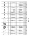
- FIG. 11 in accordance with an embodiment of the invention, is a sequence table used to set the switches in order to make measurements necessary for calculating s-parameters of a four port DUT using the TDNA shown in FIG. 4 ;
- FIG. 12 in accordance with an embodiment of the invention, is a sequence table used to set the switches in order to make measurements necessary for calculating s-parameters of a three port DUT using the TDNA shown in FIG. 4 ;
- FIG. 13 in accordance with an embodiment of the invention, is a preferred way of converting different two port s-parameter measurements of the fixture into one six port s-parameter measurement of the fixture;
- FIG. 14 in accordance with an embodiment of the invention, is a sequence table used to set the switches in order to make measurements necessary for calculating s-parameters of a two port DUT by manually calibrating the TDNA shown in FIG. 4 .
- FIG. 4 shows a preferred embodiment of a TDNA for measuring s-parameters of a DUT with four or less ports in accordance with an embodiment of the invention.
- the TDNA has one pulser and two samplers.
- the block “P-S” is preferably connected to a port marked S 1 is the pulser-sampler consisting of the pulser and the first sampler.
- the block “S” is preferably connected to port marked S 2 is the other sampler.
- RS 1 , RS 3 , RS 4 , RD 1 , RD 2 , RD 3 and RD 4 represent different switches, such that their common input connection (denoted by C) can be connected to any one of the several output connections (marked by numbers).
- These switches can be relays, PIN diodes, Micro electromechanical (MEM) switch or any other similar device.
- RS 1 may be a single pole six throw relay with six possible output connections. The common input of the relay can be connected to any one of the six output positions by switching the relay using an external control signal.
- RD 1 may be a single pole three throw relay with three possible output connections.
- S, O, and L collectively coupled to RS 1 are the short, open and load calibration standards respectively.
- T being selectively coupled to RD 1 , RD 2 , RD 3 and RD 4 is a termination device used to terminate a port if not in use.
- a DUT may be connected to ports marked D 1 , D 2 , D 3 and D 4 .
- S 1 and S 2 are the two system ports and may be referred to as the input ports of the six port fixture, and ports D 1 through D 4 may be referred to as the output ports of the fixture.
- Each switch may be switched to a position through an external control, or other central control system.
- the switch RS 1 can be switched to any one of the positions marked by numbers ranging from two to seven. If RS 1 is switched to position three, then input port S 1 is now connected to the open calibration standard marked as O.
- An example of a step measured by the pulser-sampler when RS 1 is switched to open calibration standards is shown in FIG. 5 . Any step measured by the sampler in the pulser-sampler is a combination of the input step as well as the reflected signal from port S 1 . Such a step is referred to as the reflected step, since it corresponds to the reflections at port S 1 due to the input stimulus.
- the reflections can be either due to the calibration standards, or due to any of the DUT ports connected to S 1 .
- a thru calibration standard is the path that connects input port S 1 to the other input port S 2 . This can be achieved by switching RS 1 to position seven and simultaneously switching RS 4 to position six.
- an input step applied at port S 1 is transmitted through the thru calibration standard and may be measured at port S 2 .
- FIG. 6 shows the reflected step at port S 1 measured by the pulser-sampler when the input ports are connected via the thru standard.
- FIG. 7 shows the step that goes through the thru standard and is measured by the other sampler connected to the input port marked S 2 .
- the step measured by this sampler can either be transmitted via the thru calibration standard or via the DUT through the DUT-ports connected to input ports S 1 and S 2 . Such a step is referred to as the transmitted step.
- calibrating the TDNA requires the knowledge of these calibration standards, they are measured at the time of manufacture and stored in a file preferably internal to the fixture. Thus for an automatic SOLT type of calibration method there will preferably be four files saved on the disk. This can be achieved by using a VNA or a similar instrument with high dynamic range.
- different calibration standards may preferably be connected instead of the ones indicated above. Indeed, any number of calibration standards may be connected by using additional switches. For example a switch similar to RS 1 may be used to connect six additional calibration standards. In order to do so, one may connect the common port of the new switch, say RS 2 , to unused position five of RS 1 . One then may switch RS 1 to position five and RS 2 to the position where the desired calibration standard is connected. Thus one may connect either multiple short, open, load or thru standards for SOLT type calibration or one may connect different standards depending on the calibration technique preferred.
- the calibration standards are connected to the pulser and samplers at the interface of S 1 and S 2 .
- this is the reference plane of the unit.
- Non-idealities in pulser and sampler and the cables and connectors used to connect the pulser and sampler to ports S 1 and S 2 will be accounted for by the calibration algorithm and any raw s-parameter measurements at this reference plane can be converted to a calibrated measurement.
- both measurements can be made simultaneously.
- S 22 and S 32 one needs to apply the input stimulus to port two of the DUT and measure the reflected step from port two and the transmitted step from port three of the DUT respectively. This can be achieved by switching the RS 1 to position six, thereby connecting it to RS 3 . Simultaneously switching RS 3 to position three and RD 2 to position two, to connect RD 2 and RS 3 provides the desired result.
- a connection is created between the pulser and port two of the DUT that is connected to fixture port marked D 2 .
- the pulser can apply the input to port two of the DUT, and measure the reflections from the same port.
- To measure the reflections from port three of the DUT one only needs to make a connection between the sampler and the fixture port marked D 3 . This is achieved by switching RS 4 to position four and simultaneously switching RD 3 to position four. Also terminate ports one and four of the DUT by the known termination. This is achieved by switching the switches RD 1 and RD 4 to position two. Once all the switch positions are set, an input stimulus is applied by the pulser-sampler and reflections measured by the pulser-sampler and the other sampler.
- TDNA in accordance with the various embodiments of the present invention in order to preferably measure s-parameters of a multiple port DUT with fewer pulsers and samplers
- the inventors of the present invention have developed a number of different fixture types.
- two or more fixtures may be connected to each other, or pulser and samplers can be connected to each fixture.
- a basic fixture [ 6 ], shown and described above in FIG. 4 may be used in the inventive TDNA to measure the s-parameters of up to four port DUT. This fixture may be modified so that it can be extended to connect to other fixtures.
- TDNA module [ 7 ] shown in FIG. 8 may be connected to the ports marked O 1 and O 2 of the TDNA shown in FIG.
- FIG. 9 is an example of such a TDNA.
- a TDNA capable of measuring s-parameters of a DUT with up to eight ports can be constructed by combining two TDNA's capable of measuring s-parameters of a DUT with up to four ports.
- such a TDNA will have two pulsers and four samplers.
- FIG. 4 may be used to measure DUT of two ports, there are other variations possible in accordance with various alternative embodiments of the invention based on the number of pulsers, calibration standards and or switches to be employed.
- FIG. 10 depicts a TDNA that uses two pulsers to measure s-parameters of up to two port DUT.
- switches are preferably clicked automatically and step measurements are made by the pulser-sampler and the sampler. These steps and any measurements relating thereof are then saved before proceeding to the next DUT measurement.
- the inventors of the present invention describe a sequence table depicting various sequences of operations to be performed. Each entry of the table depicts one or more switch positions for a particular calibration measurement or a DUT measurement to be made.
- a sequence table may be different if the number of DUT ports is changed.
- FIG. 11 depicts a sequence table used for measuring the s-parameter of a four port DUT connected to the TDNA shown in FIG. 4 .
- port one of the DUT is connected to the TDNA port marked D 1
- port two of the DUT is connected to the TDNA port marked D 2
- port three of the DUT is connected to the TDNA port marked D 3
- port four of the DUT is connected to the TDNA port marked D 4 .
- Column one [ 11 ] in the table shown in FIG. 11 describes the measurement number. Such a measurement number is a way to index the measurements.
- Second column [ 12 ] indicates the type of the measurement, i.e. whether it is a calibration measurement (referred to as Cal) or a DUT measurement (referred to as Dut). Since the TDNA uses a SOLT calibration technique, the table in FIG. 11 describes the switch connections for such a calibration method.
- Column three [ 13 ] indicates whether the measurement is made by the sampler in the pulser-sampler. A true indicates that the step is the reflected step measured by the sampler in the pulser-sampler and a false indicates that the step is a transmitted step measured by the other sampler.
- Column four [ 14 ] has the DUT port number that is excited by the input. For calibration measurement, none of the DUT ports are excited and hence the value is zero. Similarly column five [ 15 ] has the DUT port number that is connected to the sampler. Again for calibration measurement, none of the DUT ports are measured and hence the value is zero.
- Column six [ 16 ] indicates the connection for switch RS 1 . For example, for measurement number one, RS 1 is connected to a short calibration standard and hence an S in that position. Similarly column seven to twelve indicate the connections for switches RS 3 , RS 4 , RD 1 , RD 2 , RD 3 and RD 4 respectively. For example, for measurement number seven, DUT port one is driven and DUT port two is measured.
- switches are switched so that port one of the DUT is connected to the pulser, port two of the DUT is connected to the sampler, ports three and four of the DUT are connected to the known termination.
- the table describes the switch settings for such a case: RS 1 is connected to RS 3 , RS 3 is connected to RD 1 , RS 4 is connected to RD 2 , RD 1 is connected to RS 3 , RD 2 is connected to RS 4 and switches RD 3 and RD 4 are connected to their respective load calibration standard.
- the first five measurements are calibration measurements for SOLT calibration type.
- the input ports are connected to each other through switches RS 1 and RS 3 .
- the reflected step is measured by the pulser-sampler and for measurement five the transmitted step is measured by the other sampler. Since both of these measurements can be made at the same time, both the measurements have the same switch settings.
- the switch settings for DUT measurements are repeated. For example, measurement number six and seven have the same switch settings, measurement numbers eight and nine have the same switch settings and so on. This is the case because, for each of the DUT measurements, the same DUT port is excited and the measurements are made by the pulser-sampler in one and by the sampler in the other.
- DUT port two is excited with the input stimulus and the reflected step from the same port is measured by the pulser-sampler.
- DUT port two is excited and the step transmitted from DUT port two to DUT port one is measured by the sampler. Both the measurements can be made simultaneously.
- There are a total of twenty four DUT measurements in the sequence table. Ideally one requires only sixteen measurements (square of DUT ports), but there are more shown and employed because the measurements for S ii ,i ⁇ 1, 2, 3, 4 are repeated thrice. That is because S ii is measured each time S ij ,j i, j ⁇ 1, 2, 3, 4 is measured.
- the algorithm (described in the above-referenced copending patent application Ser. No. 13/017,394, filed Jan. 31, 2011, titled Time domain reflectometry step to s-parameter conversion) used to calculate the DUT s-parameters is able to handle such multiple measurements.
- a sequence table is prepared for the particular set of measurements, is then read by the program, and the switches switched for each measurement number. At each of the steps measurements are made and stored along with other relevant information like the measurement type, driven DUT port and measured DUT port etc. Once the steps for a row in the sequence table are saved, the process proceeds to the next measurement number and the procedure is repeated. If the number of DUT ports is different from four, then the sequence table will be different. For example, if the number of DUT ports is three, then a possible sequence table is shown in FIG. 12 (assuming that the DUT ports one through three are connected to TDNA ports marked D 1 through D 3 respectively).
- One way to characterize the fixture for each measurement condition is to remove the pulser and sampler connected to the fixture. Now the fixture is effectively a six-port passive component.
- a VNA or a VNA-like instrument can be used to measure the s-parameters of a six-port fixture.
- the switches may be set as described in the corresponding row, and the s-parameters can be measured and stored in a file. Note that for the DUT measurements, some switch connections are repeated. For this case of characterizing the fixture only one measurement for each switch configuration is required.
- Another possible way of characterizing the fixture in accordance with an embodiment of the invention is to identify all possible switch paths in the fixture.
- the possible switch paths are that from S 1 to D 1 , S 1 to D 2 , S 1 to D 3 , S 1 to D 4 , S 1 to S, S 1 to O, S 1 to L, S 1 to S 2 , S 2 to D 1 , S 2 to D 2 , S 2 to D 3 , S 2 to D 4 , D 1 to T, D 2 to T, D 3 to T and D 4 to T.
- the possible switch paths are that from S 1 to D 1 , S 1 to D 2 , S 1 to D 3 , S 1 to D 4 , S 1 to S, S 1 to O, S 1 to L, S 1 to S 2 , S 2 to D 1 , S 2 to D 2 , S 2 to D 3 , S 2 to D 4 , D 1 to T, D 2 to T, D 3 to T and D 4 to T.
- nine are two port measurements while seven are one port
- FIG. 13 demonstrates one way of converting the two port and one port s-parameter measurements into a six port fixture [ 14 ] s-parameter.
- FIG. 13 corresponds to the fixture for measurement number six and seven in the sequence table show in FIG. 11 .
- Sequence table for manual calibration for measuring two port DUT is described in FIG. 14 .
- the sequence assumes that the DUT is connected to ports D 1 and D 2 of the TDNA unit.
- the first three rows of the table describe the switch connections to perform a one-port calibration for port D 1 .
- switch RS 1 is connected to RS 3
- RS 3 is connected to RS 1
- RS 4 is connected to RD 2
- RD 1 is connected to RS 3 and RD 2 through RD 4 are connected to L.
- a known one port calibration standard is then connected to port D 1 , an input signal is applied and reflections are measured by the pulser. Similarly, measurements four to six describe the switch connections to calibrate port D 2 .
- the known one port calibration standard is then connected to port D 2 , the input signal is applied and the reflections are measured by the pulser.
- a known through standard is connected between ports D 1 and D 2 .
- the switches are set according to measurement condition seven. The input signal is applied and reflections measured by both the pulser and sampler.
- the switches are set according to measurement condition nine. The input signal is applied and reflections measured by both the pulser and sampler.
- the proposed system in accordance with the various described embodiments of the invention is therefore capable of measuring the d port DUT s-parameters by using only one pulser and two samplers.
- the algorithm (described in the above-referenced copending patent application Ser. No. 13/017,394, filed Jan. 31, 2011, titled Time domain reflectometry step to s-parameter conversion) used to calculate the DUT s-parameters is able to operate with more than one pulser and sampler, if available.
Abstract
Description
is the transfer function for port k that characterizes the reflection coefficient of port k. Here ak is the frequency domain representation of the input signal to port k of the DUT and bk is the frequency domain representation of the signal reflected from port k of the DUT. All the other ports of the DUT are terminated so that no signal reflects from those ports. Similarly,
defines the transmission coefficient between ports k and j. Here ak is the frequency domain representation of the input signal to port k of the DUT and bj is the frequency domain representation of the signal that gets transmitted from port k of the DUT to port j of the DUT. All the other ports of the DUT are terminated so that no signal reflects from those ports. Also, under ideal conditions, the sampler is such that it does not reflect any incoming signal. To measure the s-parameters of the d port DUT [1], reflected waves received at, and returned via, the d ports of the device would be measured under d independent measurement conditions. The equations that relate, for each measurement condition mε{1, . . . , d}, the reflected waves to the incident waves are shown in
where, for iε{1, . . . , d}, aim is a complex number corresponding to amplitude and phase of the incident wave at port i under measurement condition m, and where bim is a complex number corresponding to amplitude and phase of the reflected wave at port i under measurement condition m. Ideally, one would apply stimuli to each of the d ports under d unique measurement conditions (i.e., define the incident waves aim) and then measure the reflected waves at each of the d ports under these d measurement conditions (i.e., measure bim) in order to determine the unknown s-parameters. If the matrices A−(aim) and B−(bim) are defined, then the matrix S−(sim) of unknown s-parameters is S−B·A−1.
-
- The calibration is performed manually by connecting the calibration standards at the end of the measuring instrument. Besides being a time consuming exercise prone to operator errors, it also results in the mechanical wear and tear of the calibration standards.
- The number of pulser-sampler blocks increases with the number of DUT ports, thereby increasing the cost of providing a device to perform such measurements. To circumvent the problem, there have been proposed methods that use a switch matrix that connects a two port VNA or VNA-like instrument to an N-port DUT. For example U.S. Pat. No. 5,578,932 by Vahe Adamian provides one such description.
- Currently there are automatic calibration instruments available. U.S. Pat. No. 5,587,934 by Oldfield et al. provides one such description. But even these instruments suffer from the limitation of manually connecting them to the measuring device for calibration and disconnecting them to connect the DUT to the measuring instrument.
-
- setting the fixture to a particular configuration,
- applying input to one of the system ports, and
- measuring the response (reflected waves) of the system at the I system ports
are defined as a measurement condition. Thus, in accordance with the invention, the system may automatically and sequentially define multiple independent measurement conditions by using different fixture configurations and different pulser ports. Reflected waves at the I system ports may be measured under M independent measurement conditions to determine the DUT s-parameters.
-
- One or more pulsers and two or more samplers.
- A control system to apply an input signal through any desired pulser and to measure the reflected waveforms by the sampler.
- Fixtures consisting of switches, internal calibration standards, terminations and cables connecting them.
- A control to set the switches in a desired configuration.
- A software medium that stores the s-parameters of fixtures under different conditions.
- A system that consumes the measurements made by the pulsers and samplers, and the stored fixture s-parameters and calculates the s-parameters of the DUT as described in this patent.
-
- Disconnect any pulsers and/or samplers from the input ports S1 and S2.
- Connect port one of a calibrated VNA to S1 and port two of the calibrated VNA to S2.
- Switch RS1 to position two. Port one of the VNA is now connected to Short calibration standard. Save the VNA measurement and identify it as the short calibration standard.
- Switch RS1 to position three. Port one of the VNA is now connected to Open calibration standard. Save the VNA measurement and identify it as the open calibration standard.
- Switch RS1 to position four. Port one of the VNA is now connected to Load calibration standard. Save the VNA measurement and identify it as the load calibration standard.
- Switch RS1 to position seven and simultaneously switching RS4 to position six. The thru standard is now connected between the two ports of the VNA. Save the VNA measurement and identify it as the thru calibration standard.
Claims (24)
Priority Applications (1)
| Application Number | Priority Date | Filing Date | Title |
|---|---|---|---|
| US14/197,312 US9366743B2 (en) | 2010-02-01 | 2014-03-05 | Time domain network analyzer |
Applications Claiming Priority (3)
| Application Number | Priority Date | Filing Date | Title |
|---|---|---|---|
| US30006510P | 2010-02-01 | 2010-02-01 | |
| US13/017,360 US8706438B2 (en) | 2010-02-01 | 2011-01-31 | Time domain network analyzer |
| US14/197,312 US9366743B2 (en) | 2010-02-01 | 2014-03-05 | Time domain network analyzer |
Related Parent Applications (1)
| Application Number | Title | Priority Date | Filing Date |
|---|---|---|---|
| US13/017,360 Continuation US8706438B2 (en) | 2010-02-01 | 2011-01-31 | Time domain network analyzer |
Publications (2)
| Publication Number | Publication Date |
|---|---|
| US20140176156A1 US20140176156A1 (en) | 2014-06-26 |
| US9366743B2 true US9366743B2 (en) | 2016-06-14 |
Family
ID=44342372
Family Applications (2)
| Application Number | Title | Priority Date | Filing Date |
|---|---|---|---|
| US13/017,360 Active 2032-01-12 US8706438B2 (en) | 2010-02-01 | 2011-01-31 | Time domain network analyzer |
| US14/197,312 Active US9366743B2 (en) | 2010-02-01 | 2014-03-05 | Time domain network analyzer |
Family Applications Before (1)
| Application Number | Title | Priority Date | Filing Date |
|---|---|---|---|
| US13/017,360 Active 2032-01-12 US8706438B2 (en) | 2010-02-01 | 2011-01-31 | Time domain network analyzer |
Country Status (1)
| Country | Link |
|---|---|
| US (2) | US8706438B2 (en) |
Cited By (116)
| Publication number | Priority date | Publication date | Assignee | Title |
|---|---|---|---|---|
| US9674711B2 (en) | 2013-11-06 | 2017-06-06 | At&T Intellectual Property I, L.P. | Surface-wave communications and methods thereof |
| US9685992B2 (en) | 2014-10-03 | 2017-06-20 | At&T Intellectual Property I, L.P. | Circuit panel network and methods thereof |
| US9705610B2 (en) | 2014-10-21 | 2017-07-11 | At&T Intellectual Property I, L.P. | Transmission device with impairment compensation and methods for use therewith |
| US9705561B2 (en) | 2015-04-24 | 2017-07-11 | At&T Intellectual Property I, L.P. | Directional coupling device and methods for use therewith |
| US9729197B2 (en) | 2015-10-01 | 2017-08-08 | At&T Intellectual Property I, L.P. | Method and apparatus for communicating network management traffic over a network |
| US9735833B2 (en) | 2015-07-31 | 2017-08-15 | At&T Intellectual Property I, L.P. | Method and apparatus for communications management in a neighborhood network |
| US9742521B2 (en) | 2014-11-20 | 2017-08-22 | At&T Intellectual Property I, L.P. | Transmission device with mode division multiplexing and methods for use therewith |
| US9742462B2 (en) | 2014-12-04 | 2017-08-22 | At&T Intellectual Property I, L.P. | Transmission medium and communication interfaces and methods for use therewith |
| US9748626B2 (en) | 2015-05-14 | 2017-08-29 | At&T Intellectual Property I, L.P. | Plurality of cables having different cross-sectional shapes which are bundled together to form a transmission medium |
| US9749013B2 (en) | 2015-03-17 | 2017-08-29 | At&T Intellectual Property I, L.P. | Method and apparatus for reducing attenuation of electromagnetic waves guided by a transmission medium |
| US9749053B2 (en) | 2015-07-23 | 2017-08-29 | At&T Intellectual Property I, L.P. | Node device, repeater and methods for use therewith |
| US9769128B2 (en) | 2015-09-28 | 2017-09-19 | At&T Intellectual Property I, L.P. | Method and apparatus for encryption of communications over a network |
| US9768833B2 (en) | 2014-09-15 | 2017-09-19 | At&T Intellectual Property I, L.P. | Method and apparatus for sensing a condition in a transmission medium of electromagnetic waves |
| US9769020B2 (en) | 2014-10-21 | 2017-09-19 | At&T Intellectual Property I, L.P. | Method and apparatus for responding to events affecting communications in a communication network |
| US9780834B2 (en) | 2014-10-21 | 2017-10-03 | At&T Intellectual Property I, L.P. | Method and apparatus for transmitting electromagnetic waves |
| US9787412B2 (en) | 2015-06-25 | 2017-10-10 | At&T Intellectual Property I, L.P. | Methods and apparatus for inducing a fundamental wave mode on a transmission medium |
| US9793955B2 (en) | 2015-04-24 | 2017-10-17 | At&T Intellectual Property I, Lp | Passive electrical coupling device and methods for use therewith |
| US9793951B2 (en) | 2015-07-15 | 2017-10-17 | At&T Intellectual Property I, L.P. | Method and apparatus for launching a wave mode that mitigates interference |
| US9793954B2 (en) | 2015-04-28 | 2017-10-17 | At&T Intellectual Property I, L.P. | Magnetic coupling device and methods for use therewith |
| US9800327B2 (en) | 2014-11-20 | 2017-10-24 | At&T Intellectual Property I, L.P. | Apparatus for controlling operations of a communication device and methods thereof |
| US9820146B2 (en) | 2015-06-12 | 2017-11-14 | At&T Intellectual Property I, L.P. | Method and apparatus for authentication and identity management of communicating devices |
| US9838078B2 (en) | 2015-07-31 | 2017-12-05 | At&T Intellectual Property I, L.P. | Method and apparatus for exchanging communication signals |
| US9838896B1 (en) | 2016-12-09 | 2017-12-05 | At&T Intellectual Property I, L.P. | Method and apparatus for assessing network coverage |
| US9847850B2 (en) | 2014-10-14 | 2017-12-19 | At&T Intellectual Property I, L.P. | Method and apparatus for adjusting a mode of communication in a communication network |
| US9847566B2 (en) | 2015-07-14 | 2017-12-19 | At&T Intellectual Property I, L.P. | Method and apparatus for adjusting a field of a signal to mitigate interference |
| US9853342B2 (en) | 2015-07-14 | 2017-12-26 | At&T Intellectual Property I, L.P. | Dielectric transmission medium connector and methods for use therewith |
| US9860075B1 (en) | 2016-08-26 | 2018-01-02 | At&T Intellectual Property I, L.P. | Method and communication node for broadband distribution |
| US9865911B2 (en) | 2015-06-25 | 2018-01-09 | At&T Intellectual Property I, L.P. | Waveguide system for slot radiating first electromagnetic waves that are combined into a non-fundamental wave mode second electromagnetic wave on a transmission medium |
| US9866276B2 (en) | 2014-10-10 | 2018-01-09 | At&T Intellectual Property I, L.P. | Method and apparatus for arranging communication sessions in a communication system |
| US9866309B2 (en) | 2015-06-03 | 2018-01-09 | At&T Intellectual Property I, Lp | Host node device and methods for use therewith |
| US9871283B2 (en) | 2015-07-23 | 2018-01-16 | At&T Intellectual Property I, Lp | Transmission medium having a dielectric core comprised of plural members connected by a ball and socket configuration |
| US9871282B2 (en) | 2015-05-14 | 2018-01-16 | At&T Intellectual Property I, L.P. | At least one transmission medium having a dielectric surface that is covered at least in part by a second dielectric |
| US9871558B2 (en) | 2014-10-21 | 2018-01-16 | At&T Intellectual Property I, L.P. | Guided-wave transmission device and methods for use therewith |
| US9876605B1 (en) | 2016-10-21 | 2018-01-23 | At&T Intellectual Property I, L.P. | Launcher and coupling system to support desired guided wave mode |
| US9876570B2 (en) | 2015-02-20 | 2018-01-23 | At&T Intellectual Property I, Lp | Guided-wave transmission device with non-fundamental mode propagation and methods for use therewith |
| US9876264B2 (en) | 2015-10-02 | 2018-01-23 | At&T Intellectual Property I, Lp | Communication system, guided wave switch and methods for use therewith |
| US9882257B2 (en) | 2015-07-14 | 2018-01-30 | At&T Intellectual Property I, L.P. | Method and apparatus for launching a wave mode that mitigates interference |
| US9887447B2 (en) | 2015-05-14 | 2018-02-06 | At&T Intellectual Property I, L.P. | Transmission medium having multiple cores and methods for use therewith |
| US9893795B1 (en) | 2016-12-07 | 2018-02-13 | At&T Intellectual Property I, Lp | Method and repeater for broadband distribution |
| US9904535B2 (en) | 2015-09-14 | 2018-02-27 | At&T Intellectual Property I, L.P. | Method and apparatus for distributing software |
| US9906269B2 (en) | 2014-09-17 | 2018-02-27 | At&T Intellectual Property I, L.P. | Monitoring and mitigating conditions in a communication network |
| US9911020B1 (en) | 2016-12-08 | 2018-03-06 | At&T Intellectual Property I, L.P. | Method and apparatus for tracking via a radio frequency identification device |
| US9912381B2 (en) | 2015-06-03 | 2018-03-06 | At&T Intellectual Property I, Lp | Network termination and methods for use therewith |
| US9912027B2 (en) | 2015-07-23 | 2018-03-06 | At&T Intellectual Property I, L.P. | Method and apparatus for exchanging communication signals |
| US9913139B2 (en) | 2015-06-09 | 2018-03-06 | At&T Intellectual Property I, L.P. | Signal fingerprinting for authentication of communicating devices |
| US9912033B2 (en) | 2014-10-21 | 2018-03-06 | At&T Intellectual Property I, Lp | Guided wave coupler, coupling module and methods for use therewith |
| US9917341B2 (en) | 2015-05-27 | 2018-03-13 | At&T Intellectual Property I, L.P. | Apparatus and method for launching electromagnetic waves and for modifying radial dimensions of the propagating electromagnetic waves |
| US9927517B1 (en) | 2016-12-06 | 2018-03-27 | At&T Intellectual Property I, L.P. | Apparatus and methods for sensing rainfall |
| US9929755B2 (en) | 2015-07-14 | 2018-03-27 | At&T Intellectual Property I, L.P. | Method and apparatus for coupling an antenna to a device |
| US9954287B2 (en) | 2014-11-20 | 2018-04-24 | At&T Intellectual Property I, L.P. | Apparatus for converting wireless signals and electromagnetic waves and methods thereof |
| US9954286B2 (en) | 2014-10-21 | 2018-04-24 | At&T Intellectual Property I, L.P. | Guided-wave transmission device with non-fundamental mode propagation and methods for use therewith |
| US9967173B2 (en) | 2015-07-31 | 2018-05-08 | At&T Intellectual Property I, L.P. | Method and apparatus for authentication and identity management of communicating devices |
| US9973940B1 (en) | 2017-02-27 | 2018-05-15 | At&T Intellectual Property I, L.P. | Apparatus and methods for dynamic impedance matching of a guided wave launcher |
| US9973416B2 (en) | 2014-10-02 | 2018-05-15 | At&T Intellectual Property I, L.P. | Method and apparatus that provides fault tolerance in a communication network |
| US9991580B2 (en) | 2016-10-21 | 2018-06-05 | At&T Intellectual Property I, L.P. | Launcher and coupling system for guided wave mode cancellation |
| US9998870B1 (en) | 2016-12-08 | 2018-06-12 | At&T Intellectual Property I, L.P. | Method and apparatus for proximity sensing |
| US9997819B2 (en) | 2015-06-09 | 2018-06-12 | At&T Intellectual Property I, L.P. | Transmission medium and method for facilitating propagation of electromagnetic waves via a core |
| US9999038B2 (en) | 2013-05-31 | 2018-06-12 | At&T Intellectual Property I, L.P. | Remote distributed antenna system |
| US10009067B2 (en) | 2014-12-04 | 2018-06-26 | At&T Intellectual Property I, L.P. | Method and apparatus for configuring a communication interface |
| US10020844B2 (en) | 2016-12-06 | 2018-07-10 | T&T Intellectual Property I, L.P. | Method and apparatus for broadcast communication via guided waves |
| US10027397B2 (en) | 2016-12-07 | 2018-07-17 | At&T Intellectual Property I, L.P. | Distributed antenna system and methods for use therewith |
| US10044409B2 (en) | 2015-07-14 | 2018-08-07 | At&T Intellectual Property I, L.P. | Transmission medium and methods for use therewith |
| US10051630B2 (en) | 2013-05-31 | 2018-08-14 | At&T Intellectual Property I, L.P. | Remote distributed antenna system |
| US10069185B2 (en) | 2015-06-25 | 2018-09-04 | At&T Intellectual Property I, L.P. | Methods and apparatus for inducing a non-fundamental wave mode on a transmission medium |
| US10069535B2 (en) | 2016-12-08 | 2018-09-04 | At&T Intellectual Property I, L.P. | Apparatus and methods for launching electromagnetic waves having a certain electric field structure |
| US10090606B2 (en) | 2015-07-15 | 2018-10-02 | At&T Intellectual Property I, L.P. | Antenna system with dielectric array and methods for use therewith |
| US10090594B2 (en) | 2016-11-23 | 2018-10-02 | At&T Intellectual Property I, L.P. | Antenna system having structural configurations for assembly |
| US10103422B2 (en) | 2016-12-08 | 2018-10-16 | At&T Intellectual Property I, L.P. | Method and apparatus for mounting network devices |
| US10135147B2 (en) | 2016-10-18 | 2018-11-20 | At&T Intellectual Property I, L.P. | Apparatus and methods for launching guided waves via an antenna |
| US10135145B2 (en) | 2016-12-06 | 2018-11-20 | At&T Intellectual Property I, L.P. | Apparatus and methods for generating an electromagnetic wave along a transmission medium |
| US10139820B2 (en) | 2016-12-07 | 2018-11-27 | At&T Intellectual Property I, L.P. | Method and apparatus for deploying equipment of a communication system |
| US10148016B2 (en) | 2015-07-14 | 2018-12-04 | At&T Intellectual Property I, L.P. | Apparatus and methods for communicating utilizing an antenna array |
| US10168695B2 (en) | 2016-12-07 | 2019-01-01 | At&T Intellectual Property I, L.P. | Method and apparatus for controlling an unmanned aircraft |
| US10178445B2 (en) | 2016-11-23 | 2019-01-08 | At&T Intellectual Property I, L.P. | Methods, devices, and systems for load balancing between a plurality of waveguides |
| US10205655B2 (en) | 2015-07-14 | 2019-02-12 | At&T Intellectual Property I, L.P. | Apparatus and methods for communicating utilizing an antenna array and multiple communication paths |
| US10224634B2 (en) | 2016-11-03 | 2019-03-05 | At&T Intellectual Property I, L.P. | Methods and apparatus for adjusting an operational characteristic of an antenna |
| US10225025B2 (en) | 2016-11-03 | 2019-03-05 | At&T Intellectual Property I, L.P. | Method and apparatus for detecting a fault in a communication system |
| US10243270B2 (en) | 2016-12-07 | 2019-03-26 | At&T Intellectual Property I, L.P. | Beam adaptive multi-feed dielectric antenna system and methods for use therewith |
| US10243784B2 (en) | 2014-11-20 | 2019-03-26 | At&T Intellectual Property I, L.P. | System for generating topology information and methods thereof |
| US10264586B2 (en) | 2016-12-09 | 2019-04-16 | At&T Mobility Ii Llc | Cloud-based packet controller and methods for use therewith |
| US10291334B2 (en) | 2016-11-03 | 2019-05-14 | At&T Intellectual Property I, L.P. | System for detecting a fault in a communication system |
| US10298293B2 (en) | 2017-03-13 | 2019-05-21 | At&T Intellectual Property I, L.P. | Apparatus of communication utilizing wireless network devices |
| US10305190B2 (en) | 2016-12-01 | 2019-05-28 | At&T Intellectual Property I, L.P. | Reflecting dielectric antenna system and methods for use therewith |
| US10312567B2 (en) | 2016-10-26 | 2019-06-04 | At&T Intellectual Property I, L.P. | Launcher with planar strip antenna and methods for use therewith |
| US10326494B2 (en) | 2016-12-06 | 2019-06-18 | At&T Intellectual Property I, L.P. | Apparatus for measurement de-embedding and methods for use therewith |
| US10326689B2 (en) | 2016-12-08 | 2019-06-18 | At&T Intellectual Property I, L.P. | Method and system for providing alternative communication paths |
| US10340983B2 (en) | 2016-12-09 | 2019-07-02 | At&T Intellectual Property I, L.P. | Method and apparatus for surveying remote sites via guided wave communications |
| US10340603B2 (en) | 2016-11-23 | 2019-07-02 | At&T Intellectual Property I, L.P. | Antenna system having shielded structural configurations for assembly |
| US10340601B2 (en) | 2016-11-23 | 2019-07-02 | At&T Intellectual Property I, L.P. | Multi-antenna system and methods for use therewith |
| US10340573B2 (en) | 2016-10-26 | 2019-07-02 | At&T Intellectual Property I, L.P. | Launcher with cylindrical coupling device and methods for use therewith |
| US10355367B2 (en) | 2015-10-16 | 2019-07-16 | At&T Intellectual Property I, L.P. | Antenna structure for exchanging wireless signals |
| US10359749B2 (en) | 2016-12-07 | 2019-07-23 | At&T Intellectual Property I, L.P. | Method and apparatus for utilities management via guided wave communication |
| US10361489B2 (en) | 2016-12-01 | 2019-07-23 | At&T Intellectual Property I, L.P. | Dielectric dish antenna system and methods for use therewith |
| US10374316B2 (en) | 2016-10-21 | 2019-08-06 | At&T Intellectual Property I, L.P. | System and dielectric antenna with non-uniform dielectric |
| US10382976B2 (en) | 2016-12-06 | 2019-08-13 | At&T Intellectual Property I, L.P. | Method and apparatus for managing wireless communications based on communication paths and network device positions |
| US10389029B2 (en) | 2016-12-07 | 2019-08-20 | At&T Intellectual Property I, L.P. | Multi-feed dielectric antenna system with core selection and methods for use therewith |
| US10389037B2 (en) | 2016-12-08 | 2019-08-20 | At&T Intellectual Property I, L.P. | Apparatus and methods for selecting sections of an antenna array and use therewith |
| US10411356B2 (en) | 2016-12-08 | 2019-09-10 | At&T Intellectual Property I, L.P. | Apparatus and methods for selectively targeting communication devices with an antenna array |
| US10439675B2 (en) | 2016-12-06 | 2019-10-08 | At&T Intellectual Property I, L.P. | Method and apparatus for repeating guided wave communication signals |
| US10446936B2 (en) | 2016-12-07 | 2019-10-15 | At&T Intellectual Property I, L.P. | Multi-feed dielectric antenna system and methods for use therewith |
| US10498044B2 (en) | 2016-11-03 | 2019-12-03 | At&T Intellectual Property I, L.P. | Apparatus for configuring a surface of an antenna |
| US10530505B2 (en) | 2016-12-08 | 2020-01-07 | At&T Intellectual Property I, L.P. | Apparatus and methods for launching electromagnetic waves along a transmission medium |
| US10535928B2 (en) | 2016-11-23 | 2020-01-14 | At&T Intellectual Property I, L.P. | Antenna system and methods for use therewith |
| US10547348B2 (en) | 2016-12-07 | 2020-01-28 | At&T Intellectual Property I, L.P. | Method and apparatus for switching transmission mediums in a communication system |
| US10601494B2 (en) | 2016-12-08 | 2020-03-24 | At&T Intellectual Property I, L.P. | Dual-band communication device and method for use therewith |
| US10637149B2 (en) | 2016-12-06 | 2020-04-28 | At&T Intellectual Property I, L.P. | Injection molded dielectric antenna and methods for use therewith |
| US10650940B2 (en) | 2015-05-15 | 2020-05-12 | At&T Intellectual Property I, L.P. | Transmission medium having a conductive material and methods for use therewith |
| US10694379B2 (en) | 2016-12-06 | 2020-06-23 | At&T Intellectual Property I, L.P. | Waveguide system with device-based authentication and methods for use therewith |
| US10727599B2 (en) | 2016-12-06 | 2020-07-28 | At&T Intellectual Property I, L.P. | Launcher with slot antenna and methods for use therewith |
| US10755542B2 (en) | 2016-12-06 | 2020-08-25 | At&T Intellectual Property I, L.P. | Method and apparatus for surveillance via guided wave communication |
| US10777873B2 (en) | 2016-12-08 | 2020-09-15 | At&T Intellectual Property I, L.P. | Method and apparatus for mounting network devices |
| US10797781B2 (en) | 2015-06-03 | 2020-10-06 | At&T Intellectual Property I, L.P. | Client node device and methods for use therewith |
| US10811767B2 (en) | 2016-10-21 | 2020-10-20 | At&T Intellectual Property I, L.P. | System and dielectric antenna with convex dielectric radome |
| US10819035B2 (en) | 2016-12-06 | 2020-10-27 | At&T Intellectual Property I, L.P. | Launcher with helical antenna and methods for use therewith |
| US10916969B2 (en) | 2016-12-08 | 2021-02-09 | At&T Intellectual Property I, L.P. | Method and apparatus for providing power using an inductive coupling |
| US10938108B2 (en) | 2016-12-08 | 2021-03-02 | At&T Intellectual Property I, L.P. | Frequency selective multi-feed dielectric antenna system and methods for use therewith |
Families Citing this family (2)
| Publication number | Priority date | Publication date | Assignee | Title |
|---|---|---|---|---|
| US10725138B2 (en) * | 2015-12-11 | 2020-07-28 | Infineon Technologies Ag | Scattering parameter calibration to a semiconductor layer |
| US11635457B2 (en) * | 2020-08-17 | 2023-04-25 | Rohde & Schwarz Gmbh & Co. Kg | Apparatus and method for performing time domain reflectormetry |
Citations (19)
| Publication number | Priority date | Publication date | Assignee | Title |
|---|---|---|---|---|
| US4507602A (en) * | 1982-08-13 | 1985-03-26 | The United States Of America As Represented By The Secretary Of The Air Force | Measurement of permittivity and permeability of microwave materials |
| US4641085A (en) * | 1984-01-09 | 1987-02-03 | Hewlett-Packard Company | Vector network analyzer with integral processor |
| US4816767A (en) * | 1984-01-09 | 1989-03-28 | Hewlett-Packard Company | Vector network analyzer with integral processor |
| US5122800A (en) * | 1989-01-26 | 1992-06-16 | Harald Philipp | Variable successive approximation converter |
| US5502392A (en) * | 1992-04-30 | 1996-03-26 | International Business Machines Corporation | Methods for the measurement of the frequency dependent complex propagation matrix, impedance matrix and admittance matrix of coupled transmission lines |
| US5578932A (en) | 1993-05-24 | 1996-11-26 | Atn Microwave, Inc. | Method and apparatus for providing and calibrating a multiport network analyzer |
| US5587934A (en) | 1993-10-21 | 1996-12-24 | Wiltron Company | Automatic VNA calibration apparatus |
| US5715183A (en) * | 1994-12-07 | 1998-02-03 | Wiltron Company | Internal automatic calibrator for vector network analyzers |
| US20020053898A1 (en) * | 2000-09-18 | 2002-05-09 | Vahe Ademian | Multiport automatic calibration device for a multiport test system |
| US6529844B1 (en) * | 1998-09-02 | 2003-03-04 | Anritsu Company | Vector network measurement system |
| US20040193382A1 (en) * | 2000-09-18 | 2004-09-30 | Adamian Vahe' A. | Method and apparatus for calibrating a multiport test system for measurement of a DUT |
| US6853198B2 (en) * | 2002-11-14 | 2005-02-08 | Agilent Technologies, Inc. | Method and apparatus for performing multiport through-reflect-line calibration and measurement |
| US20050030047A1 (en) * | 2003-08-05 | 2005-02-10 | Vahe Adamian | Method and apparatus for measuring a device under test using an improved through-reflect-line measurement calibration |
| US7030625B1 (en) * | 2005-01-18 | 2006-04-18 | Agilent Technologies, Inc. | Method and apparatus for performing a minimum connection multiport through-reflect-line calibration and measurement |
| US7075312B2 (en) * | 2001-02-10 | 2006-07-11 | Rohde & Schwarz Gmbh & Co. Kg | Method for correcting errors by de-embedding dispersion parameters network analyst and switching module |
| US7113891B2 (en) * | 2004-05-12 | 2006-09-26 | Agilent Technologies, Inc. | Multi-port scattering parameter calibration system and method |
| US7283594B1 (en) * | 1998-01-10 | 2007-10-16 | New Transducers Limited | Impedance modulation signaling |
| US7652484B2 (en) * | 2007-02-22 | 2010-01-26 | Agilent Technologies, Inc. | Self calibration apparatus and methods |
| US7924024B2 (en) * | 2007-02-20 | 2011-04-12 | Anritsu Company | Automatic calibration techniques with improved accuracy and lower complexity for high frequency vector network analyzers |
-
2011
- 2011-01-31 US US13/017,360 patent/US8706438B2/en active Active
-
2014
- 2014-03-05 US US14/197,312 patent/US9366743B2/en active Active
Patent Citations (23)
| Publication number | Priority date | Publication date | Assignee | Title |
|---|---|---|---|---|
| US4507602A (en) * | 1982-08-13 | 1985-03-26 | The United States Of America As Represented By The Secretary Of The Air Force | Measurement of permittivity and permeability of microwave materials |
| US4641085A (en) * | 1984-01-09 | 1987-02-03 | Hewlett-Packard Company | Vector network analyzer with integral processor |
| US4816767A (en) * | 1984-01-09 | 1989-03-28 | Hewlett-Packard Company | Vector network analyzer with integral processor |
| US5122800A (en) * | 1989-01-26 | 1992-06-16 | Harald Philipp | Variable successive approximation converter |
| US5502392A (en) * | 1992-04-30 | 1996-03-26 | International Business Machines Corporation | Methods for the measurement of the frequency dependent complex propagation matrix, impedance matrix and admittance matrix of coupled transmission lines |
| US5578932A (en) | 1993-05-24 | 1996-11-26 | Atn Microwave, Inc. | Method and apparatus for providing and calibrating a multiport network analyzer |
| US5587934A (en) | 1993-10-21 | 1996-12-24 | Wiltron Company | Automatic VNA calibration apparatus |
| US5715183A (en) * | 1994-12-07 | 1998-02-03 | Wiltron Company | Internal automatic calibrator for vector network analyzers |
| US7283594B1 (en) * | 1998-01-10 | 2007-10-16 | New Transducers Limited | Impedance modulation signaling |
| US6529844B1 (en) * | 1998-09-02 | 2003-03-04 | Anritsu Company | Vector network measurement system |
| US6614237B2 (en) * | 2000-09-18 | 2003-09-02 | Agilent Technologies, Inc. | Multiport automatic calibration device for a multiport test system |
| US20030173978A1 (en) * | 2000-09-18 | 2003-09-18 | Adamian Vahe?Apos; A. | Method and apparatus for calibrating a multiport test system for measurement of a dut |
| US20040193382A1 (en) * | 2000-09-18 | 2004-09-30 | Adamian Vahe' A. | Method and apparatus for calibrating a multiport test system for measurement of a DUT |
| US6826506B2 (en) * | 2000-09-18 | 2004-11-30 | Agilent Technologies, Inc. | Method and apparatus for calibrating a multiport test system for measurement of a DUT |
| US20020053898A1 (en) * | 2000-09-18 | 2002-05-09 | Vahe Ademian | Multiport automatic calibration device for a multiport test system |
| US7075312B2 (en) * | 2001-02-10 | 2006-07-11 | Rohde & Schwarz Gmbh & Co. Kg | Method for correcting errors by de-embedding dispersion parameters network analyst and switching module |
| US6853198B2 (en) * | 2002-11-14 | 2005-02-08 | Agilent Technologies, Inc. | Method and apparatus for performing multiport through-reflect-line calibration and measurement |
| US20050030047A1 (en) * | 2003-08-05 | 2005-02-10 | Vahe Adamian | Method and apparatus for measuring a device under test using an improved through-reflect-line measurement calibration |
| US7068049B2 (en) * | 2003-08-05 | 2006-06-27 | Agilent Technologies, Inc. | Method and apparatus for measuring a device under test using an improved through-reflect-line measurement calibration |
| US7113891B2 (en) * | 2004-05-12 | 2006-09-26 | Agilent Technologies, Inc. | Multi-port scattering parameter calibration system and method |
| US7030625B1 (en) * | 2005-01-18 | 2006-04-18 | Agilent Technologies, Inc. | Method and apparatus for performing a minimum connection multiport through-reflect-line calibration and measurement |
| US7924024B2 (en) * | 2007-02-20 | 2011-04-12 | Anritsu Company | Automatic calibration techniques with improved accuracy and lower complexity for high frequency vector network analyzers |
| US7652484B2 (en) * | 2007-02-22 | 2010-01-26 | Agilent Technologies, Inc. | Self calibration apparatus and methods |
Non-Patent Citations (3)
| Title |
|---|
| "Applying Error Correction to Network Analyzer Measurements", Agilent AN 1287-3 Application Note, (2002),1-16. |
| Pupalaikis, Peter J., et al., "U.S. Appl. No. 13/017,394,", filed Jan. 31, 2011, Entitled: Time Domain Reflectometry Step to S-Parameter Conversion. |
| Wittwer, Peter et al., "A General Closed-Form Solution to Mulit-Port Scattering Parameter Calculations", 72nd ARFTG Microwave Measurement Conference, (Dec. 2008),137-143. |
Cited By (129)
| Publication number | Priority date | Publication date | Assignee | Title |
|---|---|---|---|---|
| US10051630B2 (en) | 2013-05-31 | 2018-08-14 | At&T Intellectual Property I, L.P. | Remote distributed antenna system |
| US9999038B2 (en) | 2013-05-31 | 2018-06-12 | At&T Intellectual Property I, L.P. | Remote distributed antenna system |
| US9674711B2 (en) | 2013-11-06 | 2017-06-06 | At&T Intellectual Property I, L.P. | Surface-wave communications and methods thereof |
| US9768833B2 (en) | 2014-09-15 | 2017-09-19 | At&T Intellectual Property I, L.P. | Method and apparatus for sensing a condition in a transmission medium of electromagnetic waves |
| US10063280B2 (en) | 2014-09-17 | 2018-08-28 | At&T Intellectual Property I, L.P. | Monitoring and mitigating conditions in a communication network |
| US9906269B2 (en) | 2014-09-17 | 2018-02-27 | At&T Intellectual Property I, L.P. | Monitoring and mitigating conditions in a communication network |
| US9973416B2 (en) | 2014-10-02 | 2018-05-15 | At&T Intellectual Property I, L.P. | Method and apparatus that provides fault tolerance in a communication network |
| US9685992B2 (en) | 2014-10-03 | 2017-06-20 | At&T Intellectual Property I, L.P. | Circuit panel network and methods thereof |
| US9866276B2 (en) | 2014-10-10 | 2018-01-09 | At&T Intellectual Property I, L.P. | Method and apparatus for arranging communication sessions in a communication system |
| US9847850B2 (en) | 2014-10-14 | 2017-12-19 | At&T Intellectual Property I, L.P. | Method and apparatus for adjusting a mode of communication in a communication network |
| US9871558B2 (en) | 2014-10-21 | 2018-01-16 | At&T Intellectual Property I, L.P. | Guided-wave transmission device and methods for use therewith |
| US9912033B2 (en) | 2014-10-21 | 2018-03-06 | At&T Intellectual Property I, Lp | Guided wave coupler, coupling module and methods for use therewith |
| US9705610B2 (en) | 2014-10-21 | 2017-07-11 | At&T Intellectual Property I, L.P. | Transmission device with impairment compensation and methods for use therewith |
| US9960808B2 (en) | 2014-10-21 | 2018-05-01 | At&T Intellectual Property I, L.P. | Guided-wave transmission device and methods for use therewith |
| US9769020B2 (en) | 2014-10-21 | 2017-09-19 | At&T Intellectual Property I, L.P. | Method and apparatus for responding to events affecting communications in a communication network |
| US9780834B2 (en) | 2014-10-21 | 2017-10-03 | At&T Intellectual Property I, L.P. | Method and apparatus for transmitting electromagnetic waves |
| US9876587B2 (en) | 2014-10-21 | 2018-01-23 | At&T Intellectual Property I, L.P. | Transmission device with impairment compensation and methods for use therewith |
| US9954286B2 (en) | 2014-10-21 | 2018-04-24 | At&T Intellectual Property I, L.P. | Guided-wave transmission device with non-fundamental mode propagation and methods for use therewith |
| US10243784B2 (en) | 2014-11-20 | 2019-03-26 | At&T Intellectual Property I, L.P. | System for generating topology information and methods thereof |
| US9749083B2 (en) | 2014-11-20 | 2017-08-29 | At&T Intellectual Property I, L.P. | Transmission device with mode division multiplexing and methods for use therewith |
| US9800327B2 (en) | 2014-11-20 | 2017-10-24 | At&T Intellectual Property I, L.P. | Apparatus for controlling operations of a communication device and methods thereof |
| US9742521B2 (en) | 2014-11-20 | 2017-08-22 | At&T Intellectual Property I, L.P. | Transmission device with mode division multiplexing and methods for use therewith |
| US9954287B2 (en) | 2014-11-20 | 2018-04-24 | At&T Intellectual Property I, L.P. | Apparatus for converting wireless signals and electromagnetic waves and methods thereof |
| US10009067B2 (en) | 2014-12-04 | 2018-06-26 | At&T Intellectual Property I, L.P. | Method and apparatus for configuring a communication interface |
| US9742462B2 (en) | 2014-12-04 | 2017-08-22 | At&T Intellectual Property I, L.P. | Transmission medium and communication interfaces and methods for use therewith |
| US9876571B2 (en) | 2015-02-20 | 2018-01-23 | At&T Intellectual Property I, Lp | Guided-wave transmission device with non-fundamental mode propagation and methods for use therewith |
| US9876570B2 (en) | 2015-02-20 | 2018-01-23 | At&T Intellectual Property I, Lp | Guided-wave transmission device with non-fundamental mode propagation and methods for use therewith |
| US9749013B2 (en) | 2015-03-17 | 2017-08-29 | At&T Intellectual Property I, L.P. | Method and apparatus for reducing attenuation of electromagnetic waves guided by a transmission medium |
| US9831912B2 (en) | 2015-04-24 | 2017-11-28 | At&T Intellectual Property I, Lp | Directional coupling device and methods for use therewith |
| US10224981B2 (en) | 2015-04-24 | 2019-03-05 | At&T Intellectual Property I, Lp | Passive electrical coupling device and methods for use therewith |
| US9793955B2 (en) | 2015-04-24 | 2017-10-17 | At&T Intellectual Property I, Lp | Passive electrical coupling device and methods for use therewith |
| US9705561B2 (en) | 2015-04-24 | 2017-07-11 | At&T Intellectual Property I, L.P. | Directional coupling device and methods for use therewith |
| US9793954B2 (en) | 2015-04-28 | 2017-10-17 | At&T Intellectual Property I, L.P. | Magnetic coupling device and methods for use therewith |
| US9871282B2 (en) | 2015-05-14 | 2018-01-16 | At&T Intellectual Property I, L.P. | At least one transmission medium having a dielectric surface that is covered at least in part by a second dielectric |
| US9748626B2 (en) | 2015-05-14 | 2017-08-29 | At&T Intellectual Property I, L.P. | Plurality of cables having different cross-sectional shapes which are bundled together to form a transmission medium |
| US9887447B2 (en) | 2015-05-14 | 2018-02-06 | At&T Intellectual Property I, L.P. | Transmission medium having multiple cores and methods for use therewith |
| US10650940B2 (en) | 2015-05-15 | 2020-05-12 | At&T Intellectual Property I, L.P. | Transmission medium having a conductive material and methods for use therewith |
| US9917341B2 (en) | 2015-05-27 | 2018-03-13 | At&T Intellectual Property I, L.P. | Apparatus and method for launching electromagnetic waves and for modifying radial dimensions of the propagating electromagnetic waves |
| US10797781B2 (en) | 2015-06-03 | 2020-10-06 | At&T Intellectual Property I, L.P. | Client node device and methods for use therewith |
| US10050697B2 (en) | 2015-06-03 | 2018-08-14 | At&T Intellectual Property I, L.P. | Host node device and methods for use therewith |
| US9935703B2 (en) | 2015-06-03 | 2018-04-03 | At&T Intellectual Property I, L.P. | Host node device and methods for use therewith |
| US9912382B2 (en) | 2015-06-03 | 2018-03-06 | At&T Intellectual Property I, Lp | Network termination and methods for use therewith |
| US10812174B2 (en) | 2015-06-03 | 2020-10-20 | At&T Intellectual Property I, L.P. | Client node device and methods for use therewith |
| US9912381B2 (en) | 2015-06-03 | 2018-03-06 | At&T Intellectual Property I, Lp | Network termination and methods for use therewith |
| US9967002B2 (en) | 2015-06-03 | 2018-05-08 | At&T Intellectual I, Lp | Network termination and methods for use therewith |
| US9866309B2 (en) | 2015-06-03 | 2018-01-09 | At&T Intellectual Property I, Lp | Host node device and methods for use therewith |
| US9997819B2 (en) | 2015-06-09 | 2018-06-12 | At&T Intellectual Property I, L.P. | Transmission medium and method for facilitating propagation of electromagnetic waves via a core |
| US9913139B2 (en) | 2015-06-09 | 2018-03-06 | At&T Intellectual Property I, L.P. | Signal fingerprinting for authentication of communicating devices |
| US9820146B2 (en) | 2015-06-12 | 2017-11-14 | At&T Intellectual Property I, L.P. | Method and apparatus for authentication and identity management of communicating devices |
| US9787412B2 (en) | 2015-06-25 | 2017-10-10 | At&T Intellectual Property I, L.P. | Methods and apparatus for inducing a fundamental wave mode on a transmission medium |
| US10069185B2 (en) | 2015-06-25 | 2018-09-04 | At&T Intellectual Property I, L.P. | Methods and apparatus for inducing a non-fundamental wave mode on a transmission medium |
| US9865911B2 (en) | 2015-06-25 | 2018-01-09 | At&T Intellectual Property I, L.P. | Waveguide system for slot radiating first electromagnetic waves that are combined into a non-fundamental wave mode second electromagnetic wave on a transmission medium |
| US9882257B2 (en) | 2015-07-14 | 2018-01-30 | At&T Intellectual Property I, L.P. | Method and apparatus for launching a wave mode that mitigates interference |
| US9929755B2 (en) | 2015-07-14 | 2018-03-27 | At&T Intellectual Property I, L.P. | Method and apparatus for coupling an antenna to a device |
| US10148016B2 (en) | 2015-07-14 | 2018-12-04 | At&T Intellectual Property I, L.P. | Apparatus and methods for communicating utilizing an antenna array |
| US9847566B2 (en) | 2015-07-14 | 2017-12-19 | At&T Intellectual Property I, L.P. | Method and apparatus for adjusting a field of a signal to mitigate interference |
| US10044409B2 (en) | 2015-07-14 | 2018-08-07 | At&T Intellectual Property I, L.P. | Transmission medium and methods for use therewith |
| US9853342B2 (en) | 2015-07-14 | 2017-12-26 | At&T Intellectual Property I, L.P. | Dielectric transmission medium connector and methods for use therewith |
| US10205655B2 (en) | 2015-07-14 | 2019-02-12 | At&T Intellectual Property I, L.P. | Apparatus and methods for communicating utilizing an antenna array and multiple communication paths |
| US10090606B2 (en) | 2015-07-15 | 2018-10-02 | At&T Intellectual Property I, L.P. | Antenna system with dielectric array and methods for use therewith |
| US9793951B2 (en) | 2015-07-15 | 2017-10-17 | At&T Intellectual Property I, L.P. | Method and apparatus for launching a wave mode that mitigates interference |
| US9871283B2 (en) | 2015-07-23 | 2018-01-16 | At&T Intellectual Property I, Lp | Transmission medium having a dielectric core comprised of plural members connected by a ball and socket configuration |
| US9912027B2 (en) | 2015-07-23 | 2018-03-06 | At&T Intellectual Property I, L.P. | Method and apparatus for exchanging communication signals |
| US9806818B2 (en) | 2015-07-23 | 2017-10-31 | At&T Intellectual Property I, Lp | Node device, repeater and methods for use therewith |
| US9749053B2 (en) | 2015-07-23 | 2017-08-29 | At&T Intellectual Property I, L.P. | Node device, repeater and methods for use therewith |
| US9838078B2 (en) | 2015-07-31 | 2017-12-05 | At&T Intellectual Property I, L.P. | Method and apparatus for exchanging communication signals |
| US9967173B2 (en) | 2015-07-31 | 2018-05-08 | At&T Intellectual Property I, L.P. | Method and apparatus for authentication and identity management of communicating devices |
| US9735833B2 (en) | 2015-07-31 | 2017-08-15 | At&T Intellectual Property I, L.P. | Method and apparatus for communications management in a neighborhood network |
| US9904535B2 (en) | 2015-09-14 | 2018-02-27 | At&T Intellectual Property I, L.P. | Method and apparatus for distributing software |
| US9769128B2 (en) | 2015-09-28 | 2017-09-19 | At&T Intellectual Property I, L.P. | Method and apparatus for encryption of communications over a network |
| US9729197B2 (en) | 2015-10-01 | 2017-08-08 | At&T Intellectual Property I, L.P. | Method and apparatus for communicating network management traffic over a network |
| US9876264B2 (en) | 2015-10-02 | 2018-01-23 | At&T Intellectual Property I, Lp | Communication system, guided wave switch and methods for use therewith |
| US10355367B2 (en) | 2015-10-16 | 2019-07-16 | At&T Intellectual Property I, L.P. | Antenna structure for exchanging wireless signals |
| US9860075B1 (en) | 2016-08-26 | 2018-01-02 | At&T Intellectual Property I, L.P. | Method and communication node for broadband distribution |
| US10135147B2 (en) | 2016-10-18 | 2018-11-20 | At&T Intellectual Property I, L.P. | Apparatus and methods for launching guided waves via an antenna |
| US9991580B2 (en) | 2016-10-21 | 2018-06-05 | At&T Intellectual Property I, L.P. | Launcher and coupling system for guided wave mode cancellation |
| US10811767B2 (en) | 2016-10-21 | 2020-10-20 | At&T Intellectual Property I, L.P. | System and dielectric antenna with convex dielectric radome |
| US9876605B1 (en) | 2016-10-21 | 2018-01-23 | At&T Intellectual Property I, L.P. | Launcher and coupling system to support desired guided wave mode |
| US10374316B2 (en) | 2016-10-21 | 2019-08-06 | At&T Intellectual Property I, L.P. | System and dielectric antenna with non-uniform dielectric |
| US10312567B2 (en) | 2016-10-26 | 2019-06-04 | At&T Intellectual Property I, L.P. | Launcher with planar strip antenna and methods for use therewith |
| US10340573B2 (en) | 2016-10-26 | 2019-07-02 | At&T Intellectual Property I, L.P. | Launcher with cylindrical coupling device and methods for use therewith |
| US10224634B2 (en) | 2016-11-03 | 2019-03-05 | At&T Intellectual Property I, L.P. | Methods and apparatus for adjusting an operational characteristic of an antenna |
| US10225025B2 (en) | 2016-11-03 | 2019-03-05 | At&T Intellectual Property I, L.P. | Method and apparatus for detecting a fault in a communication system |
| US10291334B2 (en) | 2016-11-03 | 2019-05-14 | At&T Intellectual Property I, L.P. | System for detecting a fault in a communication system |
| US10498044B2 (en) | 2016-11-03 | 2019-12-03 | At&T Intellectual Property I, L.P. | Apparatus for configuring a surface of an antenna |
| US10090594B2 (en) | 2016-11-23 | 2018-10-02 | At&T Intellectual Property I, L.P. | Antenna system having structural configurations for assembly |
| US10340601B2 (en) | 2016-11-23 | 2019-07-02 | At&T Intellectual Property I, L.P. | Multi-antenna system and methods for use therewith |
| US10178445B2 (en) | 2016-11-23 | 2019-01-08 | At&T Intellectual Property I, L.P. | Methods, devices, and systems for load balancing between a plurality of waveguides |
| US10340603B2 (en) | 2016-11-23 | 2019-07-02 | At&T Intellectual Property I, L.P. | Antenna system having shielded structural configurations for assembly |
| US10535928B2 (en) | 2016-11-23 | 2020-01-14 | At&T Intellectual Property I, L.P. | Antenna system and methods for use therewith |
| US10361489B2 (en) | 2016-12-01 | 2019-07-23 | At&T Intellectual Property I, L.P. | Dielectric dish antenna system and methods for use therewith |
| US10305190B2 (en) | 2016-12-01 | 2019-05-28 | At&T Intellectual Property I, L.P. | Reflecting dielectric antenna system and methods for use therewith |
| US10020844B2 (en) | 2016-12-06 | 2018-07-10 | T&T Intellectual Property I, L.P. | Method and apparatus for broadcast communication via guided waves |
| US9927517B1 (en) | 2016-12-06 | 2018-03-27 | At&T Intellectual Property I, L.P. | Apparatus and methods for sensing rainfall |
| US10637149B2 (en) | 2016-12-06 | 2020-04-28 | At&T Intellectual Property I, L.P. | Injection molded dielectric antenna and methods for use therewith |
| US10694379B2 (en) | 2016-12-06 | 2020-06-23 | At&T Intellectual Property I, L.P. | Waveguide system with device-based authentication and methods for use therewith |
| US10326494B2 (en) | 2016-12-06 | 2019-06-18 | At&T Intellectual Property I, L.P. | Apparatus for measurement de-embedding and methods for use therewith |
| US10439675B2 (en) | 2016-12-06 | 2019-10-08 | At&T Intellectual Property I, L.P. | Method and apparatus for repeating guided wave communication signals |
| US10382976B2 (en) | 2016-12-06 | 2019-08-13 | At&T Intellectual Property I, L.P. | Method and apparatus for managing wireless communications based on communication paths and network device positions |
| US10727599B2 (en) | 2016-12-06 | 2020-07-28 | At&T Intellectual Property I, L.P. | Launcher with slot antenna and methods for use therewith |
| US10755542B2 (en) | 2016-12-06 | 2020-08-25 | At&T Intellectual Property I, L.P. | Method and apparatus for surveillance via guided wave communication |
| US10135145B2 (en) | 2016-12-06 | 2018-11-20 | At&T Intellectual Property I, L.P. | Apparatus and methods for generating an electromagnetic wave along a transmission medium |
| US10819035B2 (en) | 2016-12-06 | 2020-10-27 | At&T Intellectual Property I, L.P. | Launcher with helical antenna and methods for use therewith |
| US10359749B2 (en) | 2016-12-07 | 2019-07-23 | At&T Intellectual Property I, L.P. | Method and apparatus for utilities management via guided wave communication |
| US10547348B2 (en) | 2016-12-07 | 2020-01-28 | At&T Intellectual Property I, L.P. | Method and apparatus for switching transmission mediums in a communication system |
| US10027397B2 (en) | 2016-12-07 | 2018-07-17 | At&T Intellectual Property I, L.P. | Distributed antenna system and methods for use therewith |
| US10139820B2 (en) | 2016-12-07 | 2018-11-27 | At&T Intellectual Property I, L.P. | Method and apparatus for deploying equipment of a communication system |
| US10389029B2 (en) | 2016-12-07 | 2019-08-20 | At&T Intellectual Property I, L.P. | Multi-feed dielectric antenna system with core selection and methods for use therewith |
| US10168695B2 (en) | 2016-12-07 | 2019-01-01 | At&T Intellectual Property I, L.P. | Method and apparatus for controlling an unmanned aircraft |
| US9893795B1 (en) | 2016-12-07 | 2018-02-13 | At&T Intellectual Property I, Lp | Method and repeater for broadband distribution |
| US10243270B2 (en) | 2016-12-07 | 2019-03-26 | At&T Intellectual Property I, L.P. | Beam adaptive multi-feed dielectric antenna system and methods for use therewith |
| US10446936B2 (en) | 2016-12-07 | 2019-10-15 | At&T Intellectual Property I, L.P. | Multi-feed dielectric antenna system and methods for use therewith |
| US10601494B2 (en) | 2016-12-08 | 2020-03-24 | At&T Intellectual Property I, L.P. | Dual-band communication device and method for use therewith |
| US10389037B2 (en) | 2016-12-08 | 2019-08-20 | At&T Intellectual Property I, L.P. | Apparatus and methods for selecting sections of an antenna array and use therewith |
| US10938108B2 (en) | 2016-12-08 | 2021-03-02 | At&T Intellectual Property I, L.P. | Frequency selective multi-feed dielectric antenna system and methods for use therewith |
| US10916969B2 (en) | 2016-12-08 | 2021-02-09 | At&T Intellectual Property I, L.P. | Method and apparatus for providing power using an inductive coupling |
| US10069535B2 (en) | 2016-12-08 | 2018-09-04 | At&T Intellectual Property I, L.P. | Apparatus and methods for launching electromagnetic waves having a certain electric field structure |
| US10326689B2 (en) | 2016-12-08 | 2019-06-18 | At&T Intellectual Property I, L.P. | Method and system for providing alternative communication paths |
| US10411356B2 (en) | 2016-12-08 | 2019-09-10 | At&T Intellectual Property I, L.P. | Apparatus and methods for selectively targeting communication devices with an antenna array |
| US10103422B2 (en) | 2016-12-08 | 2018-10-16 | At&T Intellectual Property I, L.P. | Method and apparatus for mounting network devices |
| US9998870B1 (en) | 2016-12-08 | 2018-06-12 | At&T Intellectual Property I, L.P. | Method and apparatus for proximity sensing |
| US10530505B2 (en) | 2016-12-08 | 2020-01-07 | At&T Intellectual Property I, L.P. | Apparatus and methods for launching electromagnetic waves along a transmission medium |
| US10777873B2 (en) | 2016-12-08 | 2020-09-15 | At&T Intellectual Property I, L.P. | Method and apparatus for mounting network devices |
| US9911020B1 (en) | 2016-12-08 | 2018-03-06 | At&T Intellectual Property I, L.P. | Method and apparatus for tracking via a radio frequency identification device |
| US10340983B2 (en) | 2016-12-09 | 2019-07-02 | At&T Intellectual Property I, L.P. | Method and apparatus for surveying remote sites via guided wave communications |
| US9838896B1 (en) | 2016-12-09 | 2017-12-05 | At&T Intellectual Property I, L.P. | Method and apparatus for assessing network coverage |
| US10264586B2 (en) | 2016-12-09 | 2019-04-16 | At&T Mobility Ii Llc | Cloud-based packet controller and methods for use therewith |
| US9973940B1 (en) | 2017-02-27 | 2018-05-15 | At&T Intellectual Property I, L.P. | Apparatus and methods for dynamic impedance matching of a guided wave launcher |
| US10298293B2 (en) | 2017-03-13 | 2019-05-21 | At&T Intellectual Property I, L.P. | Apparatus of communication utilizing wireless network devices |
Also Published As
| Publication number | Publication date |
|---|---|
| US20140176156A1 (en) | 2014-06-26 |
| US20110191054A1 (en) | 2011-08-04 |
| US8706438B2 (en) | 2014-04-22 |
Similar Documents
| Publication | Publication Date | Title |
|---|---|---|
| US9366743B2 (en) | Time domain network analyzer | |
| US6853198B2 (en) | Method and apparatus for performing multiport through-reflect-line calibration and measurement | |
| KR100456493B1 (en) | Multi-port device analysis apparatus and method and calibration method thereof | |
| Marks | Formulations of the basic vector network analyzer error model including switch-terms | |
| US6882160B2 (en) | Methods and computer program products for full N-port vector network analyzer calibrations | |
| US6188968B1 (en) | Removing effects of adapters present during vector network analyzer calibration | |
| US8860434B2 (en) | Method of measuring scattering parameters of device under test | |
| US7030625B1 (en) | Method and apparatus for performing a minimum connection multiport through-reflect-line calibration and measurement | |
| US6653848B2 (en) | Method and apparatus for linear characterization of multi-terminal single-ended or balanced devices | |
| US9176174B1 (en) | Systems and methods for simultaneously measuring forward and reverse scattering parameters | |
| US9921287B2 (en) | Method for calibrating a test rig | |
| CN104515907B (en) | A kind of scattering parameter test system and its implementation | |
| TWI627417B (en) | Vector network power meter | |
| US6690722B1 (en) | Method for characterizing frequency translation devices | |
| EP2853911A1 (en) | Two port vector network analyzer using de-embed probes | |
| US20140098848A1 (en) | Time Domain Reflectometry Step to S-Parameter Conversion | |
| US7002335B2 (en) | Method for measuring a three-port device using a two-port vector network analyzer | |
| US7113891B2 (en) | Multi-port scattering parameter calibration system and method | |
| US7739063B2 (en) | Nonlinear measurement system error correction | |
| US6396285B1 (en) | Method and apparatus for efficient measurement of reciprocal multiport devices in vector network analysis | |
| Martens et al. | Multiport vector network analyzer measurements | |
| US20240039644A1 (en) | Measurement application device calibration unit, measurement system, method | |
| JP6389354B2 (en) | Total network characteristic measuring method and apparatus | |
| US20240039647A1 (en) | Measurement application device calibration unit, measurement system, method | |
| Daniel | Development of enhanced multiport network analyzer calibrations using non-ideal standards |
Legal Events
| Date | Code | Title | Description |
|---|---|---|---|
| AS | Assignment |
Owner name: LECROY CORPORATION, NEW YORK Free format text: ASSIGNMENT OF ASSIGNORS INTEREST;ASSIGNORS:PUPALAIKIS, PETER J;DOSHI, KAVIYESH;DELBUE, ROGER;AND OTHERS;REEL/FRAME:032351/0268 Effective date: 20110128 |
|
| STCF | Information on status: patent grant |
Free format text: PATENTED CASE |
|
| MAFP | Maintenance fee payment |
Free format text: PAYMENT OF MAINTENANCE FEE, 4TH YEAR, LARGE ENTITY (ORIGINAL EVENT CODE: M1551); ENTITY STATUS OF PATENT OWNER: LARGE ENTITY Year of fee payment: 4 |
|
| MAFP | Maintenance fee payment |
Free format text: PAYMENT OF MAINTENANCE FEE, 8TH YEAR, LARGE ENTITY (ORIGINAL EVENT CODE: M1552); ENTITY STATUS OF PATENT OWNER: LARGE ENTITY Year of fee payment: 8 |