US9397312B2 - Process for fabricating metal bus lines for OLED lighting panels - Google Patents
Process for fabricating metal bus lines for OLED lighting panels Download PDFInfo
- Publication number
- US9397312B2 US9397312B2 US13/788,321 US201313788321A US9397312B2 US 9397312 B2 US9397312 B2 US 9397312B2 US 201313788321 A US201313788321 A US 201313788321A US 9397312 B2 US9397312 B2 US 9397312B2
- Authority
- US
- United States
- Prior art keywords
- bus lines
- panel
- layer
- electrode layer
- sidewall
- Prior art date
- Legal status (The legal status is an assumption and is not a legal conclusion. Google has not performed a legal analysis and makes no representation as to the accuracy of the status listed.)
- Active, expires
Links
- 238000000034 method Methods 0.000 title abstract description 61
- 230000008569 process Effects 0.000 title abstract description 35
- 229910052751 metal Inorganic materials 0.000 title description 62
- 239000002184 metal Substances 0.000 title description 62
- 238000007740 vapor deposition Methods 0.000 claims abstract description 13
- 238000005229 chemical vapour deposition Methods 0.000 claims abstract description 12
- 238000002207 thermal evaporation Methods 0.000 claims abstract description 9
- 238000001704 evaporation Methods 0.000 claims abstract description 6
- 230000008020 evaporation Effects 0.000 claims abstract description 6
- 238000004544 sputter deposition Methods 0.000 claims abstract description 6
- 239000010410 layer Substances 0.000 claims description 186
- 239000012044 organic layer Substances 0.000 claims description 48
- 238000000151 deposition Methods 0.000 claims description 21
- 238000000059 patterning Methods 0.000 claims description 17
- 239000012212 insulator Substances 0.000 claims description 15
- 230000008021 deposition Effects 0.000 claims description 11
- 230000003746 surface roughness Effects 0.000 claims description 6
- 238000000206 photolithography Methods 0.000 abstract description 13
- 230000007704 transition Effects 0.000 abstract description 12
- 238000004519 manufacturing process Methods 0.000 abstract description 11
- 238000013461 design Methods 0.000 abstract description 3
- 239000000463 material Substances 0.000 description 76
- 239000000758 substrate Substances 0.000 description 30
- 239000003446 ligand Substances 0.000 description 23
- 150000001875 compounds Chemical class 0.000 description 20
- -1 arylkyl Chemical group 0.000 description 18
- 239000002019 doping agent Substances 0.000 description 16
- RAXXELZNTBOGNW-UHFFFAOYSA-N imidazole Natural products C1=CNC=N1 RAXXELZNTBOGNW-UHFFFAOYSA-N 0.000 description 12
- 150000003384 small molecules Chemical class 0.000 description 12
- 125000003118 aryl group Chemical group 0.000 description 11
- 230000000903 blocking effect Effects 0.000 description 11
- 239000007924 injection Substances 0.000 description 10
- 238000002347 injection Methods 0.000 description 10
- 229910052757 nitrogen Inorganic materials 0.000 description 10
- 0 C*(CCCCC*)C(*1)N1[In]C Chemical compound C*(CCCCC*)C(*1)N1[In]C 0.000 description 9
- 229920000642 polymer Polymers 0.000 description 9
- VYPSYNLAJGMNEJ-UHFFFAOYSA-N Silicium dioxide Chemical compound O=[Si]=O VYPSYNLAJGMNEJ-UHFFFAOYSA-N 0.000 description 8
- 238000004770 highest occupied molecular orbital Methods 0.000 description 8
- 238000004768 lowest unoccupied molecular orbital Methods 0.000 description 8
- 239000011368 organic material Substances 0.000 description 8
- 230000032258 transport Effects 0.000 description 8
- 125000000217 alkyl group Chemical group 0.000 description 7
- IYYZUPMFVPLQIF-UHFFFAOYSA-N dibenzothiophene Chemical compound C1=CC=C2C3=CC=CC=C3SC2=C1 IYYZUPMFVPLQIF-UHFFFAOYSA-N 0.000 description 7
- 125000001072 heteroaryl group Chemical group 0.000 description 7
- 125000002524 organometallic group Chemical group 0.000 description 7
- 238000001878 scanning electron micrograph Methods 0.000 description 7
- FCEHBMOGCRZNNI-UHFFFAOYSA-N 1-benzothiophene Chemical compound C1=CC=C2SC=CC2=C1 FCEHBMOGCRZNNI-UHFFFAOYSA-N 0.000 description 6
- IJGRMHOSHXDMSA-UHFFFAOYSA-N Atomic nitrogen Chemical compound N#N IJGRMHOSHXDMSA-UHFFFAOYSA-N 0.000 description 6
- UHOVQNZJYSORNB-UHFFFAOYSA-N Benzene Chemical compound C1=CC=CC=C1 UHOVQNZJYSORNB-UHFFFAOYSA-N 0.000 description 6
- 230000007547 defect Effects 0.000 description 6
- 230000005525 hole transport Effects 0.000 description 6
- 230000005693 optoelectronics Effects 0.000 description 6
- XSCHRSMBECNVNS-UHFFFAOYSA-N quinoxaline Chemical compound N1=CC=NC2=CC=CC=C21 XSCHRSMBECNVNS-UHFFFAOYSA-N 0.000 description 6
- 239000000243 solution Substances 0.000 description 6
- 125000001424 substituent group Chemical group 0.000 description 6
- DHDHJYNTEFLIHY-UHFFFAOYSA-N 4,7-diphenyl-1,10-phenanthroline Chemical group C1=CC=CC=C1C1=CC=NC2=C1C=CC1=C(C=3C=CC=CC=3)C=CN=C21 DHDHJYNTEFLIHY-UHFFFAOYSA-N 0.000 description 5
- 125000003342 alkenyl group Chemical group 0.000 description 5
- 125000000304 alkynyl group Chemical group 0.000 description 5
- 239000000412 dendrimer Substances 0.000 description 5
- 229920000736 dendritic polymer Polymers 0.000 description 5
- TXCDCPKCNAJMEE-UHFFFAOYSA-N dibenzofuran Chemical compound C1=CC=C2C3=CC=CC=C3OC2=C1 TXCDCPKCNAJMEE-UHFFFAOYSA-N 0.000 description 5
- 125000004435 hydrogen atom Chemical group [H]* 0.000 description 5
- WCPAKWJPBJAGKN-UHFFFAOYSA-N oxadiazole Chemical compound C1=CON=N1 WCPAKWJPBJAGKN-UHFFFAOYSA-N 0.000 description 5
- 229910052760 oxygen Inorganic materials 0.000 description 5
- 150000003852 triazoles Chemical class 0.000 description 5
- HYZJCKYKOHLVJF-UHFFFAOYSA-N 1H-benzimidazole Chemical compound C1=CC=C2NC=NC2=C1 HYZJCKYKOHLVJF-UHFFFAOYSA-N 0.000 description 4
- UJOBWOGCFQCDNV-UHFFFAOYSA-N 9H-carbazole Chemical compound C1=CC=C2C3=CC=CC=C3NC2=C1 UJOBWOGCFQCDNV-UHFFFAOYSA-N 0.000 description 4
- YLQBMQCUIZJEEH-UHFFFAOYSA-N Furan Chemical compound C=1C=COC=1 YLQBMQCUIZJEEH-UHFFFAOYSA-N 0.000 description 4
- SIKJAQJRHWYJAI-UHFFFAOYSA-N Indole Chemical compound C1=CC=C2NC=CC2=C1 SIKJAQJRHWYJAI-UHFFFAOYSA-N 0.000 description 4
- UFWIBTONFRDIAS-UHFFFAOYSA-N Naphthalene Chemical compound C1=CC=CC2=CC=CC=C21 UFWIBTONFRDIAS-UHFFFAOYSA-N 0.000 description 4
- PCNDJXKNXGMECE-UHFFFAOYSA-N Phenazine Natural products C1=CC=CC2=NC3=CC=CC=C3N=C21 PCNDJXKNXGMECE-UHFFFAOYSA-N 0.000 description 4
- KYQCOXFCLRTKLS-UHFFFAOYSA-N Pyrazine Chemical compound C1=CN=CC=N1 KYQCOXFCLRTKLS-UHFFFAOYSA-N 0.000 description 4
- JUJWROOIHBZHMG-UHFFFAOYSA-N Pyridine Chemical compound C1=CC=NC=C1 JUJWROOIHBZHMG-UHFFFAOYSA-N 0.000 description 4
- SMWDFEZZVXVKRB-UHFFFAOYSA-N Quinoline Chemical compound N1=CC=CC2=CC=CC=C21 SMWDFEZZVXVKRB-UHFFFAOYSA-N 0.000 description 4
- YTPLMLYBLZKORZ-UHFFFAOYSA-N Thiophene Chemical compound C=1C=CSC=1 YTPLMLYBLZKORZ-UHFFFAOYSA-N 0.000 description 4
- DZBUGLKDJFMEHC-UHFFFAOYSA-N acridine Chemical compound C1=CC=CC2=CC3=CC=CC=C3N=C21 DZBUGLKDJFMEHC-UHFFFAOYSA-N 0.000 description 4
- 125000003545 alkoxy group Chemical group 0.000 description 4
- 229910052782 aluminium Inorganic materials 0.000 description 4
- XAGFODPZIPBFFR-UHFFFAOYSA-N aluminium Chemical compound [Al] XAGFODPZIPBFFR-UHFFFAOYSA-N 0.000 description 4
- MWPLVEDNUUSJAV-UHFFFAOYSA-N anthracene Chemical compound C1=CC=CC2=CC3=CC=CC=C3C=C21 MWPLVEDNUUSJAV-UHFFFAOYSA-N 0.000 description 4
- 125000006615 aromatic heterocyclic group Chemical group 0.000 description 4
- 125000003710 aryl alkyl group Chemical group 0.000 description 4
- CUFNKYGDVFVPHO-UHFFFAOYSA-N azulene Chemical compound C1=CC=CC2=CC=CC2=C1 CUFNKYGDVFVPHO-UHFFFAOYSA-N 0.000 description 4
- 230000008901 benefit Effects 0.000 description 4
- IOJUPLGTWVMSFF-UHFFFAOYSA-N benzothiazole Chemical compound C1=CC=C2SC=NC2=C1 IOJUPLGTWVMSFF-UHFFFAOYSA-N 0.000 description 4
- WDECIBYCCFPHNR-UHFFFAOYSA-N chrysene Chemical compound C1=CC=CC2=CC=C3C4=CC=CC=C4C=CC3=C21 WDECIBYCCFPHNR-UHFFFAOYSA-N 0.000 description 4
- 229910052681 coesite Inorganic materials 0.000 description 4
- 150000004696 coordination complex Chemical class 0.000 description 4
- 229910052906 cristobalite Inorganic materials 0.000 description 4
- 125000004122 cyclic group Chemical group 0.000 description 4
- ZUOUZKKEUPVFJK-UHFFFAOYSA-N diphenyl Chemical compound C1=CC=CC=C1C1=CC=CC=C1 ZUOUZKKEUPVFJK-UHFFFAOYSA-N 0.000 description 4
- 230000005684 electric field Effects 0.000 description 4
- 125000004404 heteroalkyl group Chemical group 0.000 description 4
- 125000000623 heterocyclic group Chemical group 0.000 description 4
- 229910052739 hydrogen Inorganic materials 0.000 description 4
- 239000001257 hydrogen Substances 0.000 description 4
- VVVPGLRKXQSQSZ-UHFFFAOYSA-N indolo[3,2-c]carbazole Chemical class C1=CC=CC2=NC3=C4C5=CC=CC=C5N=C4C=CC3=C21 VVVPGLRKXQSQSZ-UHFFFAOYSA-N 0.000 description 4
- AWJUIBRHMBBTKR-UHFFFAOYSA-N isoquinoline Chemical compound C1=NC=CC2=CC=CC=C21 AWJUIBRHMBBTKR-UHFFFAOYSA-N 0.000 description 4
- IBHBKWKFFTZAHE-UHFFFAOYSA-N n-[4-[4-(n-naphthalen-1-ylanilino)phenyl]phenyl]-n-phenylnaphthalen-1-amine Chemical compound C1=CC=CC=C1N(C=1C2=CC=CC=C2C=CC=1)C1=CC=C(C=2C=CC(=CC=2)N(C=2C=CC=CC=2)C=2C3=CC=CC=C3C=CC=2)C=C1 IBHBKWKFFTZAHE-UHFFFAOYSA-N 0.000 description 4
- 150000002894 organic compounds Chemical class 0.000 description 4
- YNPNZTXNASCQKK-UHFFFAOYSA-N phenanthrene Chemical compound C1=CC=C2C3=CC=CC=C3C=CC2=C1 YNPNZTXNASCQKK-UHFFFAOYSA-N 0.000 description 4
- 229910052698 phosphorus Inorganic materials 0.000 description 4
- 238000012545 processing Methods 0.000 description 4
- BBEAQIROQSPTKN-UHFFFAOYSA-N pyrene Chemical compound C1=CC=C2C=CC3=CC=CC4=CC=C1C2=C43 BBEAQIROQSPTKN-UHFFFAOYSA-N 0.000 description 4
- 229910052710 silicon Inorganic materials 0.000 description 4
- 239000000377 silicon dioxide Substances 0.000 description 4
- 229910052682 stishovite Inorganic materials 0.000 description 4
- 229910052717 sulfur Inorganic materials 0.000 description 4
- 125000005259 triarylamine group Chemical group 0.000 description 4
- 229910052905 tridymite Inorganic materials 0.000 description 4
- UHBIKXOBLZWFKM-UHFFFAOYSA-N 8-hydroxy-2-quinolinecarboxylic acid Chemical class C1=CC=C(O)C2=NC(C(=O)O)=CC=C21 UHBIKXOBLZWFKM-UHFFFAOYSA-N 0.000 description 3
- VFUDMQLBKNMONU-UHFFFAOYSA-N C1=CC2=C(C=C1)N(C1=CC=C(C3=CC=C(N4C5=C(C=CC=C5)C5=C4/C=C\C=C/5)C=C3)C=C1)C1=C2C=CC=C1 Chemical compound C1=CC2=C(C=C1)N(C1=CC=C(C3=CC=C(N4C5=C(C=CC=C5)C5=C4/C=C\C=C/5)C=C3)C=C1)C1=C2C=CC=C1 VFUDMQLBKNMONU-UHFFFAOYSA-N 0.000 description 3
- XUIMIQQOPSSXEZ-UHFFFAOYSA-N Silicon Chemical group [Si] XUIMIQQOPSSXEZ-UHFFFAOYSA-N 0.000 description 3
- 150000004982 aromatic amines Chemical class 0.000 description 3
- 125000000753 cycloalkyl group Chemical group 0.000 description 3
- 230000002950 deficient Effects 0.000 description 3
- 238000010586 diagram Methods 0.000 description 3
- 230000000694 effects Effects 0.000 description 3
- 230000008030 elimination Effects 0.000 description 3
- 238000003379 elimination reaction Methods 0.000 description 3
- 229960005544 indolocarbazole Drugs 0.000 description 3
- 239000011810 insulating material Substances 0.000 description 3
- IMKMFBIYHXBKRX-UHFFFAOYSA-M lithium;quinoline-2-carboxylate Chemical compound [Li+].C1=CC=CC2=NC(C(=O)[O-])=CC=C21 IMKMFBIYHXBKRX-UHFFFAOYSA-M 0.000 description 3
- 230000007246 mechanism Effects 0.000 description 3
- HZVOZRGWRWCICA-UHFFFAOYSA-N methanediyl Chemical compound [CH2] HZVOZRGWRWCICA-UHFFFAOYSA-N 0.000 description 3
- 238000002161 passivation Methods 0.000 description 3
- BASFCYQUMIYNBI-UHFFFAOYSA-N platinum Substances [Pt] BASFCYQUMIYNBI-UHFFFAOYSA-N 0.000 description 3
- 239000000126 substance Substances 0.000 description 3
- 238000012360 testing method Methods 0.000 description 3
- 125000005580 triphenylene group Chemical group 0.000 description 3
- 239000011701 zinc Substances 0.000 description 3
- JYEUMXHLPRZUAT-UHFFFAOYSA-N 1,2,3-triazine Chemical compound C1=CN=NN=C1 JYEUMXHLPRZUAT-UHFFFAOYSA-N 0.000 description 2
- KTZQTRPPVKQPFO-UHFFFAOYSA-N 1,2-benzoxazole Chemical compound C1=CC=C2C=NOC2=C1 KTZQTRPPVKQPFO-UHFFFAOYSA-N 0.000 description 2
- YJTKZCDBKVTVBY-UHFFFAOYSA-N 1,3-Diphenylbenzene Chemical group C1=CC=CC=C1C1=CC=CC(C=2C=CC=CC=2)=C1 YJTKZCDBKVTVBY-UHFFFAOYSA-N 0.000 description 2
- BCMCBBGGLRIHSE-UHFFFAOYSA-N 1,3-benzoxazole Chemical compound C1=CC=C2OC=NC2=C1 BCMCBBGGLRIHSE-UHFFFAOYSA-N 0.000 description 2
- FLBAYUMRQUHISI-UHFFFAOYSA-N 1,8-naphthyridine Chemical compound N1=CC=CC2=CC=CN=C21 FLBAYUMRQUHISI-UHFFFAOYSA-N 0.000 description 2
- IANQTJSKSUMEQM-UHFFFAOYSA-N 1-benzofuran Chemical compound C1=CC=C2OC=CC2=C1 IANQTJSKSUMEQM-UHFFFAOYSA-N 0.000 description 2
- BNRDGHFESOHOBF-UHFFFAOYSA-N 1-benzoselenophene Chemical compound C1=CC=C2[se]C=CC2=C1 BNRDGHFESOHOBF-UHFFFAOYSA-N 0.000 description 2
- WJFKNYWRSNBZNX-UHFFFAOYSA-N 10H-phenothiazine Chemical compound C1=CC=C2NC3=CC=CC=C3SC2=C1 WJFKNYWRSNBZNX-UHFFFAOYSA-N 0.000 description 2
- TZMSYXZUNZXBOL-UHFFFAOYSA-N 10H-phenoxazine Chemical compound C1=CC=C2NC3=CC=CC=C3OC2=C1 TZMSYXZUNZXBOL-UHFFFAOYSA-N 0.000 description 2
- BAXOFTOLAUCFNW-UHFFFAOYSA-N 1H-indazole Chemical compound C1=CC=C2C=NNC2=C1 BAXOFTOLAUCFNW-UHFFFAOYSA-N 0.000 description 2
- VEPOHXYIFQMVHW-XOZOLZJESA-N 2,3-dihydroxybutanedioic acid (2S,3S)-3,4-dimethyl-2-phenylmorpholine Chemical compound OC(C(O)C(O)=O)C(O)=O.C[C@H]1[C@@H](OCCN1C)c1ccccc1 VEPOHXYIFQMVHW-XOZOLZJESA-N 0.000 description 2
- OLGGLCIDAMICTA-UHFFFAOYSA-N 2-pyridin-2-yl-1h-indole Chemical compound N1C2=CC=CC=C2C=C1C1=CC=CC=N1 OLGGLCIDAMICTA-UHFFFAOYSA-N 0.000 description 2
- QMEQBOSUJUOXMX-UHFFFAOYSA-N 2h-oxadiazine Chemical compound N1OC=CC=N1 QMEQBOSUJUOXMX-UHFFFAOYSA-N 0.000 description 2
- BCHZICNRHXRCHY-UHFFFAOYSA-N 2h-oxazine Chemical compound N1OC=CC=C1 BCHZICNRHXRCHY-UHFFFAOYSA-N 0.000 description 2
- BWCDLEQTELFBAW-UHFFFAOYSA-N 3h-dioxazole Chemical compound N1OOC=C1 BWCDLEQTELFBAW-UHFFFAOYSA-N 0.000 description 2
- GJCOSYZMQJWQCA-UHFFFAOYSA-N 9H-xanthene Chemical compound C1=CC=C2CC3=CC=CC=C3OC2=C1 GJCOSYZMQJWQCA-UHFFFAOYSA-N 0.000 description 2
- ZOXJGFHDIHLPTG-UHFFFAOYSA-N Boron Chemical group [B] ZOXJGFHDIHLPTG-UHFFFAOYSA-N 0.000 description 2
- NSXJEEMTGWMJPY-UHFFFAOYSA-N C1=CC(N2C3=C(C=CC=C3)C3=C2C=CC=C3)=CC(C2=CC=CC(N3C4=C(C=CC=C4)C4=C3C=CC=C4)=C2)=C1 Chemical compound C1=CC(N2C3=C(C=CC=C3)C3=C2C=CC=C3)=CC(C2=CC=CC(N3C4=C(C=CC=C4)C4=C3C=CC=C4)=C2)=C1 NSXJEEMTGWMJPY-UHFFFAOYSA-N 0.000 description 2
- MZYDBGLUVPLRKR-UHFFFAOYSA-N C1=CC(N2C3=C(C=CC=C3)C3=C2C=CC=C3)=CC(N2C3=C(C=CC=C3)C3=C2C=CC=C3)=C1 Chemical compound C1=CC(N2C3=C(C=CC=C3)C3=C2C=CC=C3)=CC(N2C3=C(C=CC=C3)C3=C2C=CC=C3)=C1 MZYDBGLUVPLRKR-UHFFFAOYSA-N 0.000 description 2
- AWXGSYPUMWKTBR-UHFFFAOYSA-N C1=CC2=C(C=C1)N(C1=CC=C(N(C3=CC=C(N4C5=C(C=CC=C5)C5=C4C=CC=C5)C=C3)C3=CC=C(N4C5=C(C=CC=C5)C5=C4/C=C\C=C/5)C=C3)C=C1)C1=C2C=CC=C1 Chemical compound C1=CC2=C(C=C1)N(C1=CC=C(N(C3=CC=C(N4C5=C(C=CC=C5)C5=C4C=CC=C5)C=C3)C3=CC=C(N4C5=C(C=CC=C5)C5=C4/C=C\C=C/5)C=C3)C=C1)C1=C2C=CC=C1 AWXGSYPUMWKTBR-UHFFFAOYSA-N 0.000 description 2
- SDEFDICGRVDKPH-UHFFFAOYSA-M C1=CC2=C3C(=C1)O[AlH]N3=CC=C2 Chemical compound C1=CC2=C3C(=C1)O[AlH]N3=CC=C2 SDEFDICGRVDKPH-UHFFFAOYSA-M 0.000 description 2
- RZKBYYWKDPFCMX-UHFFFAOYSA-N C1=CC=C(N(C2=CC=C(C3=CC=C(N(C4=CC=CC=C4)C4=C5SC6=C(C=CC=C6)C5=CC=C4)C=C3)C=C2)C2=CC=CC3=C2SC2=C3C=CC=C2)C=C1 Chemical compound C1=CC=C(N(C2=CC=C(C3=CC=C(N(C4=CC=CC=C4)C4=C5SC6=C(C=CC=C6)C5=CC=C4)C=C3)C=C2)C2=CC=CC3=C2SC2=C3C=CC=C2)C=C1 RZKBYYWKDPFCMX-UHFFFAOYSA-N 0.000 description 2
- GEQBRULPNIVQPP-UHFFFAOYSA-N C1=CC=C(N2C(C3=CC(C4=NC5=C(C=CC=C5)N4C4=CC=CC=C4)=CC(C4=NC5=C(C=CC=C5)N4C4=CC=CC=C4)=C3)=NC3=C2C=CC=C3)C=C1 Chemical compound C1=CC=C(N2C(C3=CC(C4=NC5=C(C=CC=C5)N4C4=CC=CC=C4)=CC(C4=NC5=C(C=CC=C5)N4C4=CC=CC=C4)=C3)=NC3=C2C=CC=C3)C=C1 GEQBRULPNIVQPP-UHFFFAOYSA-N 0.000 description 2
- RXKXRKMEOMPFJD-UHFFFAOYSA-N C1=CC=C([Si](C2=CC=CC=C2)(C2=CC=CC=C2)C2=CC3=C(C=C2)SC2=C3/C=C([Si](C3=CC=CC=C3)(C3=CC=CC=C3)C3=CC=CC=C3)\C=C/2)C=C1 Chemical compound C1=CC=C([Si](C2=CC=CC=C2)(C2=CC=CC=C2)C2=CC3=C(C=C2)SC2=C3/C=C([Si](C3=CC=CC=C3)(C3=CC=CC=C3)C3=CC=CC=C3)\C=C/2)C=C1 RXKXRKMEOMPFJD-UHFFFAOYSA-N 0.000 description 2
- NNPPMTNAJDCUHE-UHFFFAOYSA-N CC(C)C Chemical compound CC(C)C NNPPMTNAJDCUHE-UHFFFAOYSA-N 0.000 description 2
- XYYYIVRDTLXJEF-UHFFFAOYSA-L CC1=N2C3=C(C=CC=C3O[Al]2OC2=CC=C(C3=CC=CC=C3)C=C2)C=C1 Chemical compound CC1=N2C3=C(C=CC=C3O[Al]2OC2=CC=C(C3=CC=CC=C3)C=C2)C=C1 XYYYIVRDTLXJEF-UHFFFAOYSA-L 0.000 description 2
- STTGYIUESPWXOW-UHFFFAOYSA-N CC1=NC2=C(C=CC3=C2N=C(C)C=C3C2=CC=CC=C2)C(C2=CC=CC=C2)=C1 Chemical compound CC1=NC2=C(C=CC3=C2N=C(C)C=C3C2=CC=CC=C2)C(C2=CC=CC=C2)=C1 STTGYIUESPWXOW-UHFFFAOYSA-N 0.000 description 2
- YZCKVEUIGOORGS-OUBTZVSYSA-N Deuterium Chemical group [2H] YZCKVEUIGOORGS-OUBTZVSYSA-N 0.000 description 2
- ZCQWOFVYLHDMMC-UHFFFAOYSA-N Oxazole Chemical compound C1=COC=N1 ZCQWOFVYLHDMMC-UHFFFAOYSA-N 0.000 description 2
- ABLZXFCXXLZCGV-UHFFFAOYSA-N Phosphorous acid Chemical compound OP(O)=O ABLZXFCXXLZCGV-UHFFFAOYSA-N 0.000 description 2
- 239000004642 Polyimide Substances 0.000 description 2
- WTKZEGDFNFYCGP-UHFFFAOYSA-N Pyrazole Chemical compound C=1C=NNC=1 WTKZEGDFNFYCGP-UHFFFAOYSA-N 0.000 description 2
- CZPWVGJYEJSRLH-UHFFFAOYSA-N Pyrimidine Chemical compound C1=CN=CN=C1 CZPWVGJYEJSRLH-UHFFFAOYSA-N 0.000 description 2
- FZWLAAWBMGSTSO-UHFFFAOYSA-N Thiazole Chemical compound C1=CSC=N1 FZWLAAWBMGSTSO-UHFFFAOYSA-N 0.000 description 2
- SLGBZMMZGDRARJ-UHFFFAOYSA-N Triphenylene Natural products C1=CC=C2C3=CC=CC=C3C3=CC=CC=C3C2=C1 SLGBZMMZGDRARJ-UHFFFAOYSA-N 0.000 description 2
- FBVBNCGJVKIEHH-UHFFFAOYSA-N [1]benzofuro[3,2-b]pyridine Chemical compound C1=CN=C2C3=CC=CC=C3OC2=C1 FBVBNCGJVKIEHH-UHFFFAOYSA-N 0.000 description 2
- QZLAKPGRUFFNRD-UHFFFAOYSA-N [1]benzoselenolo[3,2-b]pyridine Chemical compound C1=CN=C2C3=CC=CC=C3[se]C2=C1 QZLAKPGRUFFNRD-UHFFFAOYSA-N 0.000 description 2
- WIUZHVZUGQDRHZ-UHFFFAOYSA-N [1]benzothiolo[3,2-b]pyridine Chemical compound C1=CN=C2C3=CC=CC=C3SC2=C1 WIUZHVZUGQDRHZ-UHFFFAOYSA-N 0.000 description 2
- 125000002252 acyl group Chemical group 0.000 description 2
- 125000001931 aliphatic group Chemical group 0.000 description 2
- 238000013459 approach Methods 0.000 description 2
- 150000001491 aromatic compounds Chemical class 0.000 description 2
- 125000004104 aryloxy group Chemical group 0.000 description 2
- 125000004429 atom Chemical group 0.000 description 2
- 238000000089 atomic force micrograph Methods 0.000 description 2
- RFRXIWQYSOIBDI-UHFFFAOYSA-N benzarone Chemical compound CCC=1OC2=CC=CC=C2C=1C(=O)C1=CC=C(O)C=C1 RFRXIWQYSOIBDI-UHFFFAOYSA-N 0.000 description 2
- 235000010290 biphenyl Nutrition 0.000 description 2
- 239000004305 biphenyl Substances 0.000 description 2
- UFVXQDWNSAGPHN-UHFFFAOYSA-K bis[(2-methylquinolin-8-yl)oxy]-(4-phenylphenoxy)alumane Chemical compound [Al+3].C1=CC=C([O-])C2=NC(C)=CC=C21.C1=CC=C([O-])C2=NC(C)=CC=C21.C1=CC([O-])=CC=C1C1=CC=CC=C1 UFVXQDWNSAGPHN-UHFFFAOYSA-K 0.000 description 2
- 229910052796 boron Inorganic materials 0.000 description 2
- 229910052799 carbon Inorganic materials 0.000 description 2
- 125000002915 carbonyl group Chemical group [*:2]C([*:1])=O 0.000 description 2
- 150000001735 carboxylic acids Chemical group 0.000 description 2
- WCZVZNOTHYJIEI-UHFFFAOYSA-N cinnoline Chemical compound N1=NC=CC2=CC=CC=C21 WCZVZNOTHYJIEI-UHFFFAOYSA-N 0.000 description 2
- 239000003086 colorant Substances 0.000 description 2
- 230000000052 comparative effect Effects 0.000 description 2
- 239000002322 conducting polymer Substances 0.000 description 2
- 229920001940 conductive polymer Polymers 0.000 description 2
- 238000007796 conventional method Methods 0.000 description 2
- 125000000392 cycloalkenyl group Chemical group 0.000 description 2
- 229910052805 deuterium Inorganic materials 0.000 description 2
- DHFABSXGNHDNCO-UHFFFAOYSA-N dibenzoselenophene Chemical compound C1=CC=C2C3=CC=CC=C3[se]C2=C1 DHFABSXGNHDNCO-UHFFFAOYSA-N 0.000 description 2
- 150000002148 esters Chemical group 0.000 description 2
- GVEPBJHOBDJJJI-UHFFFAOYSA-N fluoranthrene Natural products C1=CC(C2=CC=CC=C22)=C3C2=CC=CC3=C1 GVEPBJHOBDJJJI-UHFFFAOYSA-N 0.000 description 2
- RMBPEFMHABBEKP-UHFFFAOYSA-N fluorene Chemical compound C1=CC=C2C3=C[CH]C=CC3=CC2=C1 RMBPEFMHABBEKP-UHFFFAOYSA-N 0.000 description 2
- 150000002343 gold Chemical class 0.000 description 2
- PCHJSUWPFVWCPO-UHFFFAOYSA-N gold Chemical compound [Au] PCHJSUWPFVWCPO-UHFFFAOYSA-N 0.000 description 2
- 229910052737 gold Inorganic materials 0.000 description 2
- 239000010931 gold Substances 0.000 description 2
- 150000004820 halides Chemical group 0.000 description 2
- 238000005286 illumination Methods 0.000 description 2
- PZOUSPYUWWUPPK-UHFFFAOYSA-N indole Natural products CC1=CC=CC2=C1C=CN2 PZOUSPYUWWUPPK-UHFFFAOYSA-N 0.000 description 2
- RKJUIXBNRJVNHR-UHFFFAOYSA-N indolenine Natural products C1=CC=C2CC=NC2=C1 RKJUIXBNRJVNHR-UHFFFAOYSA-N 0.000 description 2
- 150000002503 iridium Chemical class 0.000 description 2
- 229910052741 iridium Inorganic materials 0.000 description 2
- UEEXRMUCXBPYOV-UHFFFAOYSA-N iridium;2-phenylpyridine Chemical group [Ir].C1=CC=CC=C1C1=CC=CC=N1.C1=CC=CC=C1C1=CC=CC=N1.C1=CC=CC=C1C1=CC=CC=N1 UEEXRMUCXBPYOV-UHFFFAOYSA-N 0.000 description 2
- 150000002527 isonitriles Chemical group 0.000 description 2
- QDLAGTHXVHQKRE-UHFFFAOYSA-N lichenxanthone Natural products COC1=CC(O)=C2C(=O)C3=C(C)C=C(OC)C=C3OC2=C1 QDLAGTHXVHQKRE-UHFFFAOYSA-N 0.000 description 2
- 239000011159 matrix material Substances 0.000 description 2
- 229910044991 metal oxide Inorganic materials 0.000 description 2
- 150000004706 metal oxides Chemical class 0.000 description 2
- 239000000203 mixture Substances 0.000 description 2
- 239000000178 monomer Substances 0.000 description 2
- 150000002825 nitriles Chemical group 0.000 description 2
- NIHNNTQXNPWCJQ-UHFFFAOYSA-N o-biphenylenemethane Natural products C1=CC=C2CC3=CC=CC=C3C2=C1 NIHNNTQXNPWCJQ-UHFFFAOYSA-N 0.000 description 2
- AZHVQJLDOFKHPZ-UHFFFAOYSA-N oxathiazine Chemical compound O1SN=CC=C1 AZHVQJLDOFKHPZ-UHFFFAOYSA-N 0.000 description 2
- CQDAMYNQINDRQC-UHFFFAOYSA-N oxatriazole Chemical compound C1=NN=NO1 CQDAMYNQINDRQC-UHFFFAOYSA-N 0.000 description 2
- 125000004430 oxygen atom Chemical group O* 0.000 description 2
- 125000002080 perylenyl group Chemical group C1(=CC=C2C=CC=C3C4=CC=CC5=CC=CC(C1=C23)=C45)* 0.000 description 2
- CSHWQDPOILHKBI-UHFFFAOYSA-N peryrene Natural products C1=CC(C2=CC=CC=3C2=C2C=CC=3)=C3C2=CC=CC3=C1 CSHWQDPOILHKBI-UHFFFAOYSA-N 0.000 description 2
- XDJOIMJURHQYDW-UHFFFAOYSA-N phenalene Chemical compound C1=CC(CC=C2)=C3C2=CC=CC3=C1 XDJOIMJURHQYDW-UHFFFAOYSA-N 0.000 description 2
- 229950000688 phenothiazine Drugs 0.000 description 2
- FVZVCSNXTFCBQU-UHFFFAOYSA-N phosphanyl Chemical group [PH2] FVZVCSNXTFCBQU-UHFFFAOYSA-N 0.000 description 2
- 125000004437 phosphorous atom Chemical group 0.000 description 2
- LFSXCDWNBUNEEM-UHFFFAOYSA-N phthalazine Chemical compound C1=NN=CC2=CC=CC=C21 LFSXCDWNBUNEEM-UHFFFAOYSA-N 0.000 description 2
- IEQIEDJGQAUEQZ-UHFFFAOYSA-N phthalocyanine Chemical compound N1C(N=C2C3=CC=CC=C3C(N=C3C4=CC=CC=C4C(=N4)N3)=N2)=C(C=CC=C2)C2=C1N=C1C2=CC=CC=C2C4=N1 IEQIEDJGQAUEQZ-UHFFFAOYSA-N 0.000 description 2
- 229910052697 platinum Inorganic materials 0.000 description 2
- 229920001721 polyimide Polymers 0.000 description 2
- 125000002924 primary amino group Chemical group [H]N([H])* 0.000 description 2
- 239000011241 protective layer Substances 0.000 description 2
- CPNGPNLZQNNVQM-UHFFFAOYSA-N pteridine Chemical compound N1=CN=CC2=NC=CN=C21 CPNGPNLZQNNVQM-UHFFFAOYSA-N 0.000 description 2
- PBMFSQRYOILNGV-UHFFFAOYSA-N pyridazine Chemical compound C1=CC=NN=C1 PBMFSQRYOILNGV-UHFFFAOYSA-N 0.000 description 2
- UMJSCPRVCHMLSP-UHFFFAOYSA-N pyridine Natural products COC1=CC=CN=C1 UMJSCPRVCHMLSP-UHFFFAOYSA-N 0.000 description 2
- JWVCLYRUEFBMGU-UHFFFAOYSA-N quinazoline Chemical compound N1=CN=CC2=CC=CC=C21 JWVCLYRUEFBMGU-UHFFFAOYSA-N 0.000 description 2
- 230000000717 retained effect Effects 0.000 description 2
- 229920006395 saturated elastomer Polymers 0.000 description 2
- 239000010703 silicon Substances 0.000 description 2
- 238000010129 solution processing Methods 0.000 description 2
- 125000000475 sulfinyl group Chemical group [*:2]S([*:1])=O 0.000 description 2
- 125000000472 sulfonyl group Chemical group *S(*)(=O)=O 0.000 description 2
- 125000004434 sulfur atom Chemical group 0.000 description 2
- VLLMWSRANPNYQX-UHFFFAOYSA-N thiadiazole Chemical compound C1=CSN=N1.C1=CSN=N1 VLLMWSRANPNYQX-UHFFFAOYSA-N 0.000 description 2
- 239000010409 thin film Substances 0.000 description 2
- 125000003396 thiol group Chemical group [H]S* 0.000 description 2
- 229930192474 thiophene Natural products 0.000 description 2
- TVIVIEFSHFOWTE-UHFFFAOYSA-K tri(quinolin-8-yloxy)alumane Chemical compound [Al+3].C1=CN=C2C([O-])=CC=CC2=C1.C1=CN=C2C([O-])=CC=CC2=C1.C1=CN=C2C([O-])=CC=CC2=C1 TVIVIEFSHFOWTE-UHFFFAOYSA-K 0.000 description 2
- XLYOFNOQVPJJNP-UHFFFAOYSA-N water Substances O XLYOFNOQVPJJNP-UHFFFAOYSA-N 0.000 description 2
- DSAFSORWJPSMQS-UHFFFAOYSA-N 10H-phenothiazine 5-oxide Chemical compound C1=CC=C2S(=O)C3=CC=CC=C3NC2=C1 DSAFSORWJPSMQS-UHFFFAOYSA-N 0.000 description 1
- MWTPXLULLUBAOP-UHFFFAOYSA-N 2-phenoxy-1,3-benzothiazole Chemical class N=1C2=CC=CC=C2SC=1OC1=CC=CC=C1 MWTPXLULLUBAOP-UHFFFAOYSA-N 0.000 description 1
- XSPQHOJEUTZTON-UHFFFAOYSA-N 2-phenoxy-1,3-benzoxazole Chemical class N=1C2=CC=CC=C2OC=1OC1=CC=CC=C1 XSPQHOJEUTZTON-UHFFFAOYSA-N 0.000 description 1
- MEAAWTRWNWSLPF-UHFFFAOYSA-N 2-phenoxypyridine Chemical class C=1C=CC=NC=1OC1=CC=CC=C1 MEAAWTRWNWSLPF-UHFFFAOYSA-N 0.000 description 1
- 150000005360 2-phenylpyridines Chemical class 0.000 description 1
- DIVZFUBWFAOMCW-UHFFFAOYSA-N 4-n-(3-methylphenyl)-1-n,1-n-bis[4-(n-(3-methylphenyl)anilino)phenyl]-4-n-phenylbenzene-1,4-diamine Chemical group CC1=CC=CC(N(C=2C=CC=CC=2)C=2C=CC(=CC=2)N(C=2C=CC(=CC=2)N(C=2C=CC=CC=2)C=2C=C(C)C=CC=2)C=2C=CC(=CC=2)N(C=2C=CC=CC=2)C=2C=C(C)C=CC=2)=C1 DIVZFUBWFAOMCW-UHFFFAOYSA-N 0.000 description 1
- BPMFPOGUJAAYHL-UHFFFAOYSA-N 9H-Pyrido[2,3-b]indole Chemical compound C1=CC=C2C3=CC=CC=C3NC2=N1 BPMFPOGUJAAYHL-UHFFFAOYSA-N 0.000 description 1
- NFWATNMVZVJXMW-UHFFFAOYSA-N 9h-carbazole;dibenzofuran Chemical class C1=CC=C2C3=CC=CC=C3NC2=C1.C1=CC=C2C3=CC=CC=C3OC2=C1 NFWATNMVZVJXMW-UHFFFAOYSA-N 0.000 description 1
- AYOMISFIGMZTGF-UHFFFAOYSA-O BrC1=CC=C(N(C2=CC=C([NH+](C3=C4C=CC=CC4=C4C=CC=CC4=C3)C3=C4C=CC=CC4=C4C=CC=CC4=C3)C=C2)C2=C3C=CC=CC3=C3C=CC=CC3=C2)C=C1 Chemical compound BrC1=CC=C(N(C2=CC=C([NH+](C3=C4C=CC=CC4=C4C=CC=CC4=C3)C3=C4C=CC=CC4=C4C=CC=CC4=C3)C=C2)C2=C3C=CC=CC3=C3C=CC=CC3=C2)C=C1 AYOMISFIGMZTGF-UHFFFAOYSA-O 0.000 description 1
- FSZHBEYFUBAVJU-UHFFFAOYSA-N C(#C[Au]12C3=CC=CC=C3C3=CC=CC(=N31)C1=CC=CC=C12)C1=CC=C(N(C2=CC=CC=C2)C2=CC=CC=C2)C=C1 Chemical compound C(#C[Au]12C3=CC=CC=C3C3=CC=CC(=N31)C1=CC=CC=C12)C1=CC=C(N(C2=CC=CC=C2)C2=CC=CC=C2)C=C1 FSZHBEYFUBAVJU-UHFFFAOYSA-N 0.000 description 1
- RVNWTQIBASUOPP-UHFFFAOYSA-N C.C.C.CCC Chemical compound C.C.C.CCC RVNWTQIBASUOPP-UHFFFAOYSA-N 0.000 description 1
- QXBUZULIIPOMBL-UHFFFAOYSA-N C/C1=C2\CC3=N(C=CC=N3)[Pt]3(\C2=C(/C)S1)N1=CC=CN1B(N1C=CC=N1)(N1C=CC=N1)N1C=CC=N13 Chemical compound C/C1=C2\CC3=N(C=CC=N3)[Pt]3(\C2=C(/C)S1)N1=CC=CN1B(N1C=CC=N1)(N1C=CC=N1)N1C=CC=N13 QXBUZULIIPOMBL-UHFFFAOYSA-N 0.000 description 1
- QKVWPNRUXZYLQV-UHFFFAOYSA-N C1=CC(C2=C/C=C3\C4=C(C=CC=C4)C4=C(C=CC=C4)\C3=C\2)=CC(C2=CC=CC3=C2SC2=C3C=CC=C2)=C1 Chemical compound C1=CC(C2=C/C=C3\C4=C(C=CC=C4)C4=C(C=CC=C4)\C3=C\2)=CC(C2=CC=CC3=C2SC2=C3C=CC=C2)=C1 QKVWPNRUXZYLQV-UHFFFAOYSA-N 0.000 description 1
- IMKXSEPQICZHSL-UHFFFAOYSA-N C1=CC(C2=CC3=C(C=C2)SC2=C3C=CC=C2)=CC(C2=CC(N3C4=C(C=CC=C4)C4=C3C=CC=C4)=CC=C2)=C1 Chemical compound C1=CC(C2=CC3=C(C=C2)SC2=C3C=CC=C2)=CC(C2=CC(N3C4=C(C=CC=C4)C4=C3C=CC=C4)=CC=C2)=C1 IMKXSEPQICZHSL-UHFFFAOYSA-N 0.000 description 1
- KFKHNBPNJMWUEG-UHFFFAOYSA-N C1=CC(C2=CC=CC(C3=CC4=C(C=C3)C3=C(C=CC=C3)C3=C4C=CC=C3)=C2)=CC(C2=CC3=C(C=C2)C2=C(C=CC=C2)C2=C3C=CC=C2)=C1 Chemical compound C1=CC(C2=CC=CC(C3=CC4=C(C=C3)C3=C(C=CC=C3)C3=C4C=CC=C3)=C2)=CC(C2=CC3=C(C=C2)C2=C(C=CC=C2)C2=C3C=CC=C2)=C1 KFKHNBPNJMWUEG-UHFFFAOYSA-N 0.000 description 1
- FEEVDOPOKYHDKB-UHFFFAOYSA-N C1=CC(C2=C\C3=C(\C=C/2)C2=C(C=CC=C2)C2=C3C=CC=C2)=CC(C2=C/C3=C(\C=C/2)C2=C(C=CC=C2)C2=C3C=CC=C2)=C1 Chemical compound C1=CC(C2=C\C3=C(\C=C/2)C2=C(C=CC=C2)C2=C3C=CC=C2)=CC(C2=C/C3=C(\C=C/2)C2=C(C=CC=C2)C2=C3C=CC=C2)=C1 FEEVDOPOKYHDKB-UHFFFAOYSA-N 0.000 description 1
- IHUZMIYPBUPXCM-UHFFFAOYSA-N C1=CC2=C(C=C1)C1=C(/C=C\C(N3C4=C(C=CC=C4)C4=C3/C=C/C(N3C5=C(C=CC=C5)C5=C3/C=C\C=C/5)=C\4)=C/1)S2 Chemical compound C1=CC2=C(C=C1)C1=C(/C=C\C(N3C4=C(C=CC=C4)C4=C3/C=C/C(N3C5=C(C=CC=C5)C5=C3/C=C\C=C/5)=C\4)=C/1)S2 IHUZMIYPBUPXCM-UHFFFAOYSA-N 0.000 description 1
- LVYJBTHSDKJVTH-UHFFFAOYSA-N C1=CC2=C(C=C1)C1=C(/C=C\C=C/1)C2.C1=CC2=C(C=C1)C1=C(/C=C\C=C/1)O2.C1=CC2=C(C=C1)C1=C(/C=C\C=C/1)S2.C1=CC2=C3C=CC=CC3=C3/C=C\C=C/C3=C2C=C1.C1=CC2=CC=C3/C=C\C=C/C3=C2C=C1.C1=CC=C(C2=CC=CC(C3=CC=CC=C3)=C2)C=C1.C1=CC=C2C=C3C=CC=CC3=CC2=C1.C1=CC=C2C=CC=CC2=C1.CC1=CC=C(C)C=C1.CN1C2=C(C=CC=C2)C2=C1/C=C\C=C/2 Chemical compound C1=CC2=C(C=C1)C1=C(/C=C\C=C/1)C2.C1=CC2=C(C=C1)C1=C(/C=C\C=C/1)O2.C1=CC2=C(C=C1)C1=C(/C=C\C=C/1)S2.C1=CC2=C3C=CC=CC3=C3/C=C\C=C/C3=C2C=C1.C1=CC2=CC=C3/C=C\C=C/C3=C2C=C1.C1=CC=C(C2=CC=CC(C3=CC=CC=C3)=C2)C=C1.C1=CC=C2C=C3C=CC=CC3=CC2=C1.C1=CC=C2C=CC=CC2=C1.CC1=CC=C(C)C=C1.CN1C2=C(C=CC=C2)C2=C1/C=C\C=C/2 LVYJBTHSDKJVTH-UHFFFAOYSA-N 0.000 description 1
- HSPZYQUMRCQDDG-UHFFFAOYSA-N C1=CC2=C(C=C1)C1=CC=C3[Ir]N4=C(C=CC=C4)C3=C1S2 Chemical compound C1=CC2=C(C=C1)C1=CC=C3[Ir]N4=C(C=CC=C4)C3=C1S2 HSPZYQUMRCQDDG-UHFFFAOYSA-N 0.000 description 1
- SDHNJSIZTIODFW-UHFFFAOYSA-N C1=CC2=C(C=C1)N(C1=CC3=C(C=C1)SC1=C3/C=C(N3C4=C(C=CC=C4)C4=C3C=CC=C4)\C=C/1)C1=C2C=CC=C1 Chemical compound C1=CC2=C(C=C1)N(C1=CC3=C(C=C1)SC1=C3/C=C(N3C4=C(C=CC=C4)C4=C3C=CC=C4)\C=C/1)C1=C2C=CC=C1 SDHNJSIZTIODFW-UHFFFAOYSA-N 0.000 description 1
- CQZOLIZFWRSNOM-UHFFFAOYSA-N C1=CC2=C(C=C1)N1CC3=CC=CC4=C3[Ir]35(C6=CN(CC7=CC=CC(=N73)CN3C=C5C5=C3C=CC=C5)C3=C6C=CC=C3)(N1=C2)N1=CC2=C(C=CC=C2)N1C4 Chemical compound C1=CC2=C(C=C1)N1CC3=CC=CC4=C3[Ir]35(C6=CN(CC7=CC=CC(=N73)CN3C=C5C5=C3C=CC=C5)C3=C6C=CC=C3)(N1=C2)N1=CC2=C(C=CC=C2)N1C4 CQZOLIZFWRSNOM-UHFFFAOYSA-N 0.000 description 1
- VDRONIBNVZLDJL-UHFFFAOYSA-N C1=CC2=C(SC3=C2/C=C\C=C/3N2C3=C(C=CC=C3)C3=C2C=CC=C3)C(N2C3=C(C=CC=C3)C3=C2C=CC=C3)=C1 Chemical compound C1=CC2=C(SC3=C2/C=C\C=C/3N2C3=C(C=CC=C3)C3=C2C=CC=C3)C(N2C3=C(C=CC=C3)C3=C2C=CC=C3)=C1 VDRONIBNVZLDJL-UHFFFAOYSA-N 0.000 description 1
- SBYMPPVIXIJQGA-UHFFFAOYSA-N C1=CC2=C3C4=C1C1=C5C4=C4C6=C\3C3=C2C=CC2=C3/C3=C\6C6=C4/C4=C5/C(=C5/C=C\C7=C8C=CC2=C3C8=C/6/C7=C/54)/C=C\1 Chemical compound C1=CC2=C3C4=C1C1=C5C4=C4C6=C\3C3=C2C=CC2=C3/C3=C\6C6=C4/C4=C5/C(=C5/C=C\C7=C8C=CC2=C3C8=C/6/C7=C/54)/C=C\1 SBYMPPVIXIJQGA-UHFFFAOYSA-N 0.000 description 1
- PCWKWGNZYZSYBS-UHFFFAOYSA-M C1=CC2=C3C=CC=CC3=C3/C=C\C=C/C3=C2C=C1.C1=CC2=CC=C3/C=C\C=N/C3=C2N=C1.C1=CC=C(N2C=NC3=C2C=CC=C3)C=C1.CC1=C(F)C(F)=C(C)C(F)=C1F.C[Al](N)O.O=S1(=O)C2=C(C=CC=C2)CC2=C1C=CC=C2 Chemical compound C1=CC2=C3C=CC=CC3=C3/C=C\C=C/C3=C2C=C1.C1=CC2=CC=C3/C=C\C=N/C3=C2N=C1.C1=CC=C(N2C=NC3=C2C=CC=C3)C=C1.CC1=C(F)C(F)=C(C)C(F)=C1F.C[Al](N)O.O=S1(=O)C2=C(C=CC=C2)CC2=C1C=CC=C2 PCWKWGNZYZSYBS-UHFFFAOYSA-M 0.000 description 1
- LABGHJUTWCOYQE-UHFFFAOYSA-N C1=CC2=CC=C(C3=CC4=C(C=C3)C=C(C3=CC=CC(C5=C6/C=C\C=C/C6=C6C=CC=CC6=C5)=C3)C=C4)C=C2C=C1 Chemical compound C1=CC2=CC=C(C3=CC4=C(C=C3)C=C(C3=CC=CC(C5=C6/C=C\C=C/C6=C6C=CC=CC6=C5)=C3)C=C4)C=C2C=C1 LABGHJUTWCOYQE-UHFFFAOYSA-N 0.000 description 1
- IZKKEYIPFTVWHN-UHFFFAOYSA-N C1=CC2=N(C=C1)[Ir]N1N=CC=C21 Chemical compound C1=CC2=N(C=C1)[Ir]N1N=CC=C21 IZKKEYIPFTVWHN-UHFFFAOYSA-N 0.000 description 1
- MKZDOOLFFBQAOV-UHFFFAOYSA-N C1=CC2=N(C=C1)[Os]N1N=CC=C21.C1=CC=C(P(C2=CC=CC=C2)C2=CC=CC=C2)C=C1 Chemical compound C1=CC2=N(C=C1)[Os]N1N=CC=C21.C1=CC=C(P(C2=CC=CC=C2)C2=CC=CC=C2)C=C1 MKZDOOLFFBQAOV-UHFFFAOYSA-N 0.000 description 1
- ABFTVLCDLFSSMI-UHFFFAOYSA-N C1=CC=C(C2=CC3=C(C=C2)[Ir]2(C4=CC=CC=C4C4=N2C=CC=C4)N2=CC=CC=C32)C=C1 Chemical compound C1=CC=C(C2=CC3=C(C=C2)[Ir]2(C4=CC=CC=C4C4=N2C=CC=C4)N2=CC=CC=C32)C=C1 ABFTVLCDLFSSMI-UHFFFAOYSA-N 0.000 description 1
- LOANKKZXVZMPBA-UHFFFAOYSA-N C1=CC=C(C2=CC3=C(C=C2)[Ir]N2=CC=CN32)C=C1 Chemical compound C1=CC=C(C2=CC3=C(C=C2)[Ir]N2=CC=CN32)C=C1 LOANKKZXVZMPBA-UHFFFAOYSA-N 0.000 description 1
- RSWOJEDGRFCGFR-UHFFFAOYSA-N C1=CC=C(C2=CC3=C(C=C2C2=CC=CC=C2)C2=C(C=C(C4=CC=CC=C4)C(C4=CC=CC=C4)=C2)C2=C3C=C(C3=CC=CC=C3)C(C3=CC=CC=C3)=C2)C=C1 Chemical compound C1=CC=C(C2=CC3=C(C=C2C2=CC=CC=C2)C2=C(C=C(C4=CC=CC=C4)C(C4=CC=CC=C4)=C2)C2=C3C=C(C3=CC=CC=C3)C(C3=CC=CC=C3)=C2)C=C1 RSWOJEDGRFCGFR-UHFFFAOYSA-N 0.000 description 1
- WXAIEIRYBSKHDP-UHFFFAOYSA-N C1=CC=C(C2=CC=C(N(C3=CC=C(C4=CC=CC=C4)C=C3)C3=CC=C(C4=CC=C(N(C5=CC=C(C6=CC=CC=C6)C=C5)C5=CC=C(C6=CC=CC=C6)C=C5)C=C4)C=C3)C=C2)C=C1 Chemical compound C1=CC=C(C2=CC=C(N(C3=CC=C(C4=CC=CC=C4)C=C3)C3=CC=C(C4=CC=C(N(C5=CC=C(C6=CC=CC=C6)C=C5)C5=CC=C(C6=CC=CC=C6)C=C5)C=C4)C=C3)C=C2)C=C1 WXAIEIRYBSKHDP-UHFFFAOYSA-N 0.000 description 1
- KQCREFMBDCFFGP-UHFFFAOYSA-N C1=CC=C(C2=CC=C(N(C3=CC=CC=C3)C3=CC=C(C4=CC=C(N(C5=CC=CC=C5)C5=CC=C(C6=CC=C(C7=CC=C(N(C8=CC=CC=C8)C8=CC=C(C9=CC=C(N(C%10=CC=CC=C%10)C%10=CC=C(C%11=CC=CC=C%11)C=C%10)C=C9)C=C8)C=C7)C=C6)C=C5)C=C4)C=C3)C=C2)C=C1 Chemical compound C1=CC=C(C2=CC=C(N(C3=CC=CC=C3)C3=CC=C(C4=CC=C(N(C5=CC=CC=C5)C5=CC=C(C6=CC=C(C7=CC=C(N(C8=CC=CC=C8)C8=CC=C(C9=CC=C(N(C%10=CC=CC=C%10)C%10=CC=C(C%11=CC=CC=C%11)C=C%10)C=C9)C=C8)C=C7)C=C6)C=C5)C=C4)C=C3)C=C2)C=C1 KQCREFMBDCFFGP-UHFFFAOYSA-N 0.000 description 1
- HTNRLCWDKMRUIH-UHFFFAOYSA-N C1=CC=C(C2=CC=N3C4=C2/C=C\C2=C(C5=CC=CC=C5)C=CN(=C24)[Pt]3(C2=CC=CC=C2)C2=CC=CC=C2)C=C1.CF.CF.FF.FF.FF.FF Chemical compound C1=CC=C(C2=CC=N3C4=C2/C=C\C2=C(C5=CC=CC=C5)C=CN(=C24)[Pt]3(C2=CC=CC=C2)C2=CC=CC=C2)C=C1.CF.CF.FF.FF.FF.FF HTNRLCWDKMRUIH-UHFFFAOYSA-N 0.000 description 1
- VBJWDGGEJNGTET-UHFFFAOYSA-N C1=CC=C(C2=NC(C3=CC=CC=C3)=NC(N3C4=C(C=CC=C4)C4=CC=C5C6=C(C=CC=C6)N(C6=CC=CC=C6)C5=C43)=N2)C=C1 Chemical compound C1=CC=C(C2=NC(C3=CC=CC=C3)=NC(N3C4=C(C=CC=C4)C4=CC=C5C6=C(C=CC=C6)N(C6=CC=CC=C6)C5=C43)=N2)C=C1 VBJWDGGEJNGTET-UHFFFAOYSA-N 0.000 description 1
- IEGZNIQHTJNUPB-UHFFFAOYSA-N C1=CC=C(C2=NC3=C(C=C2)C2=C(N=CC=C2)C2=NC=CC=C23)C=C1 Chemical compound C1=CC=C(C2=NC3=C(C=C2)C2=C(N=CC=C2)C2=NC=CC=C23)C=C1 IEGZNIQHTJNUPB-UHFFFAOYSA-N 0.000 description 1
- PHBJYIUTTPNUBD-UHFFFAOYSA-N C1=CC=C(C2=NC3=C(C=CC=C3)N2C2=CC=C(C3=C4C=CC=CC4=C(C4=CC=C5C=CC=CC5=C4)C4=C3C=CC=C4)C=C2)C=C1 Chemical compound C1=CC=C(C2=NC3=C(C=CC=C3)N2C2=CC=C(C3=C4C=CC=CC4=C(C4=CC=C5C=CC=CC5=C4)C4=C3C=CC=C4)C=C2)C=C1 PHBJYIUTTPNUBD-UHFFFAOYSA-N 0.000 description 1
- YRWIIMMGRRUDQF-UHFFFAOYSA-P C1=CC=C(C2=NN3C(=N2)C2=CC=CC=N2[Cu]32[PH](C3=CC=CC=C3)(C3=CC=CC=C3)C3=CC=CC=C3OC3=C(C=CC=C3)[PH]2(C2=CC=CC=C2)C2=CC=CC=C2)C=C1 Chemical compound C1=CC=C(C2=NN3C(=N2)C2=CC=CC=N2[Cu]32[PH](C3=CC=CC=C3)(C3=CC=CC=C3)C3=CC=CC=C3OC3=C(C=CC=C3)[PH]2(C2=CC=CC=C2)C2=CC=CC=C2)C=C1 YRWIIMMGRRUDQF-UHFFFAOYSA-P 0.000 description 1
- ICVRMAPETUQKIA-UHFFFAOYSA-N C1=CC=C(C2=NN=C(C3=CC=C(C4=NN=C(C5=CC=CC=C5)N4C4=CC=CC=C4)C=C3)O2)C=C1 Chemical compound C1=CC=C(C2=NN=C(C3=CC=C(C4=NN=C(C5=CC=CC=C5)N4C4=CC=CC=C4)C=C3)O2)C=C1 ICVRMAPETUQKIA-UHFFFAOYSA-N 0.000 description 1
- AOQKGYRILLEVJV-UHFFFAOYSA-N C1=CC=C(C2=NN=C(C3=CC=CC=C3)N2C2=CC=CC3=C2C=CC=C3)C=C1 Chemical compound C1=CC=C(C2=NN=C(C3=CC=CC=C3)N2C2=CC=CC3=C2C=CC=C3)C=C1 AOQKGYRILLEVJV-UHFFFAOYSA-N 0.000 description 1
- CRHRWHRNQKPUPO-UHFFFAOYSA-N C1=CC=C(N(C2=CC=C(N(C3=CC=C(N(C4=CC=CC=C4)C4=C5C=CC=CC5=CC=C4)C=C3)C3=CC=C(N(C4=CC=CC=C4)C4=C5C=CC=CC5=CC=C4)C=C3)C=C2)C2=C3C=CC=CC3=CC=C2)C=C1 Chemical compound C1=CC=C(N(C2=CC=C(N(C3=CC=C(N(C4=CC=CC=C4)C4=C5C=CC=CC5=CC=C4)C=C3)C3=CC=C(N(C4=CC=CC=C4)C4=C5C=CC=CC5=CC=C4)C=C3)C=C2)C2=C3C=CC=CC3=CC=C2)C=C1 CRHRWHRNQKPUPO-UHFFFAOYSA-N 0.000 description 1
- JFKLZFRYTVUCFU-MVVLPMFXSA-N C1=CC=C(N(C2=CC=C3C(=C2)C2=CC=CC=C2C2=C(C=CC=C2)C2=C3C=CC=C2)C2=CC3=C(C=C2)C2=CC=CC=C2C2=CC=CC=C2C2=C3C=CC=C2)C=C1 Chemical compound C1=CC=C(N(C2=CC=C3C(=C2)C2=CC=CC=C2C2=C(C=CC=C2)C2=C3C=CC=C2)C2=CC3=C(C=C2)C2=CC=CC=C2C2=CC=CC=C2C2=C3C=CC=C2)C=C1 JFKLZFRYTVUCFU-MVVLPMFXSA-N 0.000 description 1
- WLLRHFOXFKWDMQ-UHFFFAOYSA-N C1=CC=C(N(C2=CC=CC=C2)C2=CC=C(C3=CC=C(N(C4=CC=CC=C4)C4=CC=C(C5=CC=C(N(C6=CC=CC=C6)C6=CC=C(C7=CC=C(N(C8=CC=CC=C8)C8=CC=CC=C8)C=C7)C=C6)C=C5)C=C4)C=C3)C=C2)C=C1 Chemical compound C1=CC=C(N(C2=CC=CC=C2)C2=CC=C(C3=CC=C(N(C4=CC=CC=C4)C4=CC=C(C5=CC=C(N(C6=CC=CC=C6)C6=CC=C(C7=CC=C(N(C8=CC=CC=C8)C8=CC=CC=C8)C=C7)C=C6)C=C5)C=C4)C=C3)C=C2)C=C1 WLLRHFOXFKWDMQ-UHFFFAOYSA-N 0.000 description 1
- OWGROPIUHIMXLC-UHFFFAOYSA-L C1=CC=C(N(C2=CC=CC=C2)C2=CC=C(O[Al]3OC4=CC=CC=C4C4=N3C3=C(C=CC=C3)O4)C=C2)C=C1 Chemical compound C1=CC=C(N(C2=CC=CC=C2)C2=CC=C(O[Al]3OC4=CC=CC=C4C4=N3C3=C(C=CC=C3)O4)C=C2)C=C1 OWGROPIUHIMXLC-UHFFFAOYSA-L 0.000 description 1
- VOZBMWWMIQGZGM-UHFFFAOYSA-N C1=CC=C(N2C(C3=CC=C(C4=CC5=C(C6=CC7=C(C=CC=C7)C=C6)C6=CC=CC=C6C(C6=CC=C7C=CC=CC7=C6)=C5C=C4)C=C3)=NC3=C2C=CC=C3)C=C1 Chemical compound C1=CC=C(N2C(C3=CC=C(C4=CC5=C(C6=CC7=C(C=CC=C7)C=C6)C6=CC=CC=C6C(C6=CC=C7C=CC=CC7=C6)=C5C=C4)C=C3)=NC3=C2C=CC=C3)C=C1 VOZBMWWMIQGZGM-UHFFFAOYSA-N 0.000 description 1
- RPHSQWOMKHJGSI-UHFFFAOYSA-N C1=CC=C(N2C3=C(C=C(C4=CC(C5=CC6=C(C=C5)N(C5=CC=CC=C5)C5=C6/C=C(C6=C/C=C7/C8=C(C=CN=C8)O\C7=C/6)\C=C\5)=CC=C4)C=C3)C3=C2C=CC(C2=C\C4=C(\C=C/2)C2=C(C=CN=C2)O4)=C3)C=C1 Chemical compound C1=CC=C(N2C3=C(C=C(C4=CC(C5=CC6=C(C=C5)N(C5=CC=CC=C5)C5=C6/C=C(C6=C/C=C7/C8=C(C=CN=C8)O\C7=C/6)\C=C\5)=CC=C4)C=C3)C3=C2C=CC(C2=C\C4=C(\C=C/2)C2=C(C=CN=C2)O4)=C3)C=C1 RPHSQWOMKHJGSI-UHFFFAOYSA-N 0.000 description 1
- PFDGGTXOJGJINX-UHFFFAOYSA-N C1=CC=C(N2C3=C(C=CC=C3)N3=C2C2=CC=CC=C2[Ir]3)C=C1 Chemical compound C1=CC=C(N2C3=C(C=CC=C3)N3=C2C2=CC=CC=C2[Ir]3)C=C1 PFDGGTXOJGJINX-UHFFFAOYSA-N 0.000 description 1
- IIBIMTHLGUGVJF-UHFFFAOYSA-N C1=CC=C(N2C3=C(C=CC=C3)N3C4=C(C=CC=C4)[Ir]C23)C=C1 Chemical compound C1=CC=C(N2C3=C(C=CC=C3)N3C4=C(C=CC=C4)[Ir]C23)C=C1 IIBIMTHLGUGVJF-UHFFFAOYSA-N 0.000 description 1
- ILBCEHBXGSOZJK-UHFFFAOYSA-N C1=CC=C(N2C3=CC=CC=C3C3=C2C2=C(C=C3)C3=C(C=CC=C3)N2C2=CC=C(N3C4=C(C=CC=C4)C4=C3C3=C(C=C4)C4=CC=CC=C4N3C3=CC=CC=C3)C=C2)C=C1 Chemical compound C1=CC=C(N2C3=CC=CC=C3C3=C2C2=C(C=C3)C3=C(C=CC=C3)N2C2=CC=C(N3C4=C(C=CC=C4)C4=C3C3=C(C=C4)C4=CC=CC=C4N3C3=CC=CC=C3)C=C2)C=C1 ILBCEHBXGSOZJK-UHFFFAOYSA-N 0.000 description 1
- FLCOBMXLSOVHGE-UHFFFAOYSA-N C1=CC=C(N2C3=CC=CC=C3C3=C2C2=C(C=C3)C3=C(C=CC=C3)N2C2=CC=CC=C2)C=C1 Chemical compound C1=CC=C(N2C3=CC=CC=C3C3=C2C2=C(C=C3)C3=C(C=CC=C3)N2C2=CC=CC=C2)C=C1 FLCOBMXLSOVHGE-UHFFFAOYSA-N 0.000 description 1
- KSJBCQHLUVQQRU-UHFFFAOYSA-N C1=CC=C(N2C3=CC=CC=C3C3=CC4=C(C=C32)[Ir]N2=C4C=CC=C2)C=C1 Chemical compound C1=CC=C(N2C3=CC=CC=C3C3=CC4=C(C=C32)[Ir]N2=C4C=CC=C2)C=C1 KSJBCQHLUVQQRU-UHFFFAOYSA-N 0.000 description 1
- VNTLICYURVZKBN-UHFFFAOYSA-N C1=CC=C(N2C=CN3=C2C2=CC=CC=C2[Ir]3)C=C1 Chemical compound C1=CC=C(N2C=CN3=C2C2=CC=CC=C2[Ir]3)C=C1 VNTLICYURVZKBN-UHFFFAOYSA-N 0.000 description 1
- ROBUGAOOQWWSQP-UHFFFAOYSA-L C1=CC=C(O[Al]2OC3=CC=CC=C3C3=N2C2=C(C=CC=C2)O3)C=C1 Chemical compound C1=CC=C(O[Al]2OC3=CC=CC=C3C3=N2C2=C(C=CC=C2)O3)C=C1 ROBUGAOOQWWSQP-UHFFFAOYSA-L 0.000 description 1
- ASWCTGBIMZWXAP-UHFFFAOYSA-M C1=CC=C(O[Pt]23C4=C(C=CC=C4C4=CC=CC=N42)C2=CC=CC=N23)C=C1 Chemical compound C1=CC=C(O[Pt]23C4=C(C=CC=C4C4=CC=CC=N42)C2=CC=CC=N23)C=C1 ASWCTGBIMZWXAP-UHFFFAOYSA-M 0.000 description 1
- RNJALDUDQIQBDE-UHFFFAOYSA-N C1=CC=C([Si](C2=CC=CC=C2)(C2=CC=CC(C3=C4SC5=C(C=CC=C5)C4=CC=C3)=C2)C2=CC=CC(C3=C4SC5=C(C=CC=C5)C4=CC=C3)=C2)C=C1 Chemical compound C1=CC=C([Si](C2=CC=CC=C2)(C2=CC=CC(C3=C4SC5=C(C=CC=C5)C4=CC=C3)=C2)C2=CC=CC(C3=C4SC5=C(C=CC=C5)C4=CC=C3)=C2)C=C1 RNJALDUDQIQBDE-UHFFFAOYSA-N 0.000 description 1
- QEKZOTRGIUHUEK-UHFFFAOYSA-N C1=CC=C([Si](C2=CC=CC=C2)(C2=CC=CC=C2)C2=CC=C([Si](C3=CC=CC=C3)(C3=CC=CC=C3)C3=CC=C([Si](C4=CC=CC=C4)(C4=CC=CC=C4)C4=CC=CC=C4)C=C3)C=C2)C=C1 Chemical compound C1=CC=C([Si](C2=CC=CC=C2)(C2=CC=CC=C2)C2=CC=C([Si](C3=CC=CC=C3)(C3=CC=CC=C3)C3=CC=C([Si](C4=CC=CC=C4)(C4=CC=CC=C4)C4=CC=CC=C4)C=C3)C=C2)C=C1 QEKZOTRGIUHUEK-UHFFFAOYSA-N 0.000 description 1
- XCJYREBRNVKWGJ-UHFFFAOYSA-N C1=CC=C2C(=C1)/C1=N/C3=N4/C(=N\C5=C6C=CC=CC6=C6/N=C7/C8=C(C=CC=C8)C8=N7[Cu]4(N56)N1/C2=N\8)C1=C3C=CC=C1 Chemical compound C1=CC=C2C(=C1)/C1=N/C3=N4/C(=N\C5=C6C=CC=CC6=C6/N=C7/C8=C(C=CC=C8)C8=N7[Cu]4(N56)N1/C2=N\8)C1=C3C=CC=C1 XCJYREBRNVKWGJ-UHFFFAOYSA-N 0.000 description 1
- DISZOYLMLQLMFJ-UHFFFAOYSA-N C1=CC=C2C(=C1)C1=C(/C=C3/C4=C(C=CC=C4)N(C4=C5C=CC=CC5=CC=C4)/C3=C/1)N2C1=C2C=CC=CC2=CC=C1 Chemical compound C1=CC=C2C(=C1)C1=C(/C=C3/C4=C(C=CC=C4)N(C4=C5C=CC=CC5=CC=C4)/C3=C/1)N2C1=C2C=CC=CC2=CC=C1 DISZOYLMLQLMFJ-UHFFFAOYSA-N 0.000 description 1
- ZPXSBJSLTDIQDY-UHFFFAOYSA-N C1=CC=C2C(=C1)C1=C(/C=C\C=C/1)C2(C1=CC=C(C2=CC=C(N3C4=C(C=CC=C4)C4=C3C=CC=C4)C=C2)C=C1)C1=CC=C(C2=CC=C(N3C4=C(C=CC=C4)C4=C3C=CC=C4)C=C2)C=C1 Chemical compound C1=CC=C2C(=C1)C1=C(/C=C\C=C/1)C2(C1=CC=C(C2=CC=C(N3C4=C(C=CC=C4)C4=C3C=CC=C4)C=C2)C=C1)C1=CC=C(C2=CC=C(N3C4=C(C=CC=C4)C4=C3C=CC=C4)C=C2)C=C1 ZPXSBJSLTDIQDY-UHFFFAOYSA-N 0.000 description 1
- LYXTZYYMWXCIFZ-UHFFFAOYSA-N C1=CC=C2C(=C1)C1=C(/C=C\C=C/1)C2(C1=CC=C(OC2=CC=C(N3C4=C(C=CC=C4)C4=C3C=CC=C4)C=C2)C=C1)C1=CC=C(OC2=CC=C(N3C4=C(C=CC=C4)C4=C3C=CC=C4)C=C2)C=C1 Chemical compound C1=CC=C2C(=C1)C1=C(/C=C\C=C/1)C2(C1=CC=C(OC2=CC=C(N3C4=C(C=CC=C4)C4=C3C=CC=C4)C=C2)C=C1)C1=CC=C(OC2=CC=C(N3C4=C(C=CC=C4)C4=C3C=CC=C4)C=C2)C=C1 LYXTZYYMWXCIFZ-UHFFFAOYSA-N 0.000 description 1
- ZRRXYWGZYSXZAL-UHFFFAOYSA-N C1=CC=C2C(=C1)C1=C3C(=CC=C1)[Ir]/N1=C/SC2=C31 Chemical compound C1=CC=C2C(=C1)C1=C3C(=CC=C1)[Ir]/N1=C/SC2=C31 ZRRXYWGZYSXZAL-UHFFFAOYSA-N 0.000 description 1
- SFJCUQUQYYDZBU-UHFFFAOYSA-N C1=CC=C2C(=C1)C1=C3C(=CC=C1)[Ir]C1S/N=C/2N31 Chemical compound C1=CC=C2C(=C1)C1=C3C(=CC=C1)[Ir]C1S/N=C/2N31 SFJCUQUQYYDZBU-UHFFFAOYSA-N 0.000 description 1
- UDECAGDIODUDKR-UHFFFAOYSA-N C1=CC=C2C(=C1)C1=C3C(=CC=C1)[Ir]N1=C3N2C2=C1C=CC=C2 Chemical compound C1=CC=C2C(=C1)C1=C3C(=CC=C1)[Ir]N1=C3N2C2=C1C=CC=C2 UDECAGDIODUDKR-UHFFFAOYSA-N 0.000 description 1
- SUSUNAMVLCHRSL-UHFFFAOYSA-N C1=CC=C2C(=C1)C1=C3\C4=N(C=CN24)[Ir]\C3=C/C=C\1 Chemical compound C1=CC=C2C(=C1)C1=C3\C4=N(C=CN24)[Ir]\C3=C/C=C\1 SUSUNAMVLCHRSL-UHFFFAOYSA-N 0.000 description 1
- QKBWDYLFYVXTGE-UHFFFAOYSA-N C1=CC=C2C(=C1)C1=N(C=CC=C1)[Ir]213(C2=CC=CC=C2C2=N1C=CC=C2)C1=CC=CC=C1C1=N3C=CC=C1 Chemical compound C1=CC=C2C(=C1)C1=N(C=CC=C1)[Ir]213(C2=CC=CC=C2C2=N1C=CC=C2)C1=CC=CC=C1C1=N3C=CC=C1 QKBWDYLFYVXTGE-UHFFFAOYSA-N 0.000 description 1
- LBRNYOFFDZIUSZ-UHFFFAOYSA-N C1=CC=C2C(=C1)C1=N(C=CC=C1)[Ir]21C2=C(C=C3C(=C2)C2=N(C=CC=C2)[Ir]32C3=C(C=CC=C3)C3=C\C=C/C=N\32)C2=N1C=CC=C2 Chemical compound C1=CC=C2C(=C1)C1=N(C=CC=C1)[Ir]21C2=C(C=C3C(=C2)C2=N(C=CC=C2)[Ir]32C3=C(C=CC=C3)C3=C\C=C/C=N\32)C2=N1C=CC=C2 LBRNYOFFDZIUSZ-UHFFFAOYSA-N 0.000 description 1
- IYIUHXHCIXFOEJ-UHFFFAOYSA-M C1=CC=C2C(=C1)O[Zn]N1=C2C=CC=C1 Chemical compound C1=CC=C2C(=C1)O[Zn]N1=C2C=CC=C1 IYIUHXHCIXFOEJ-UHFFFAOYSA-M 0.000 description 1
- JTXCFSSIPVHVHI-UHFFFAOYSA-M C1=CC=C2C(=C1)O[Zn]N1=C2OC2=C1C=CC=C2 Chemical compound C1=CC=C2C(=C1)O[Zn]N1=C2OC2=C1C=CC=C2 JTXCFSSIPVHVHI-UHFFFAOYSA-M 0.000 description 1
- IPHJBEMZJPBDDQ-UHFFFAOYSA-M C1=CC=C2C(=C1)O[Zn]N1=C2SC2=C1C=CC=C2 Chemical compound C1=CC=C2C(=C1)O[Zn]N1=C2SC2=C1C=CC=C2 IPHJBEMZJPBDDQ-UHFFFAOYSA-M 0.000 description 1
- HXWLCVYLRPMRDY-UHFFFAOYSA-N C1=CC=C2C(=C1)[Ir]N1=C2C2=C(C=CC=C2)C=C1 Chemical compound C1=CC=C2C(=C1)[Ir]N1=C2C2=C(C=CC=C2)C=C1 HXWLCVYLRPMRDY-UHFFFAOYSA-N 0.000 description 1
- ZIBMOMRUIPOUQK-UHFFFAOYSA-N C1=CC=C2C(=C1)[Ir]N1=C2C=CC=C1 Chemical compound C1=CC=C2C(=C1)[Ir]N1=C2C=CC=C1 ZIBMOMRUIPOUQK-UHFFFAOYSA-N 0.000 description 1
- XMWRBQBLMFGWIX-UHFFFAOYSA-N C60 fullerene Chemical compound C12=C3C(C4=C56)=C7C8=C5C5=C9C%10=C6C6=C4C1=C1C4=C6C6=C%10C%10=C9C9=C%11C5=C8C5=C8C7=C3C3=C7C2=C1C1=C2C4=C6C4=C%10C6=C9C9=C%11C5=C5C8=C3C3=C7C1=C1C2=C4C6=C2C9=C5C3=C12 XMWRBQBLMFGWIX-UHFFFAOYSA-N 0.000 description 1
- KTHLWBLLCJDNKO-UFMFWQRBSA-M C=CC1=CC=C(CCC2=CC(C)=O[Ir]3(O2)C2=C/C=C\C=C\2C2=N3C=CC=C2)C=C1 Chemical compound C=CC1=CC=C(CCC2=CC(C)=O[Ir]3(O2)C2=C/C=C\C=C\2C2=N3C=CC=C2)C=C1 KTHLWBLLCJDNKO-UFMFWQRBSA-M 0.000 description 1
- LZHSWUZRHVYRKC-UHFFFAOYSA-N C=CC1=CC=C(N(C2=CC=C(C=C)C=C2)C2=CC=C(C3=CC4=C(C=C3)[Ir]3(C5=CC=CC=C5C5=N3C=CC=C5)N3=CC=CC=C43)C=C2)C=C1 Chemical compound C=CC1=CC=C(N(C2=CC=C(C=C)C=C2)C2=CC=C(C3=CC4=C(C=C3)[Ir]3(C5=CC=CC=C5C5=N3C=CC=C5)N3=CC=CC=C43)C=C2)C=C1 LZHSWUZRHVYRKC-UHFFFAOYSA-N 0.000 description 1
- ZVFQEOPUXVPSLB-UHFFFAOYSA-N CC(C)(C)C1=CC=C(C2=NN=C(C3=CC=C(C4=CC=CC=C4)C=C3)N2C2=CC=CC=C2)C=C1 Chemical compound CC(C)(C)C1=CC=C(C2=NN=C(C3=CC=C(C4=CC=CC=C4)C=C3)N2C2=CC=CC=C2)C=C1 ZVFQEOPUXVPSLB-UHFFFAOYSA-N 0.000 description 1
- XZCJVWCMJYNSQO-UHFFFAOYSA-N CC(C)(C)C1=CC=C(C2=NN=C(C3=CC=C(C4=CC=CC=C4)C=C3)O2)C=C1 Chemical compound CC(C)(C)C1=CC=C(C2=NN=C(C3=CC=C(C4=CC=CC=C4)C=C3)O2)C=C1 XZCJVWCMJYNSQO-UHFFFAOYSA-N 0.000 description 1
- DCOKAXQXFVCURF-UHFFFAOYSA-N CC(C)(C)C1=NN2[Ru]N3=C(C2=C1)C1=C(C=CC=C1)C=C3.CP(C)C1=CC=CC=C1.CP(C)C1=CC=CC=C1 Chemical compound CC(C)(C)C1=NN2[Ru]N3=C(C2=C1)C1=C(C=CC=C1)C=C3.CP(C)C1=CC=CC=C1.CP(C)C1=CC=CC=C1 DCOKAXQXFVCURF-UHFFFAOYSA-N 0.000 description 1
- XOWBJNIJFIUJJT-UHFFFAOYSA-N CC(C)(C1=CC=C(OC(=O)C2=CC=CC=C2)C=C1)C1=CC=C(OC(=O)C2=CC=CC=C2)C=C1 Chemical compound CC(C)(C1=CC=C(OC(=O)C2=CC=CC=C2)C=C1)C1=CC=C(OC(=O)C2=CC=CC=C2)C=C1 XOWBJNIJFIUJJT-UHFFFAOYSA-N 0.000 description 1
- FOCXDAJVTRKSCC-UHFFFAOYSA-N CC(C)NCN(CN(C)C)CN(C)C.CN(C)C.CN(C)C(N(C)C)N(C)C.CN(C)CN(C)C.CN(C)CN(C)CN(C)CN(C)C Chemical compound CC(C)NCN(CN(C)C)CN(C)C.CN(C)C.CN(C)C(N(C)C)N(C)C.CN(C)CN(C)C.CN(C)CN(C)CN(C)CN(C)C FOCXDAJVTRKSCC-UHFFFAOYSA-N 0.000 description 1
- XKIQUNRFEBRUNR-UHFFFAOYSA-N CC1(C)C2=CC=CC3=N2[Pt]2(C4=CN(C5=CC=CC=C5)N=C43)C3=C/N(C4=CC=CC=C4)/N=C\3C3=N2C1=CC=C3 Chemical compound CC1(C)C2=CC=CC3=N2[Pt]2(C4=CN(C5=CC=CC=C5)N=C43)C3=C/N(C4=CC=CC=C4)/N=C\3C3=N2C1=CC=C3 XKIQUNRFEBRUNR-UHFFFAOYSA-N 0.000 description 1
- NYKPMLPNLGNWFS-UHFFFAOYSA-N CC1=C(C2=C(F)C(F)=C(F)C(F)=C2F)C(F)=C(F)C(C2=C(F)C(C3=C(F)C(F)=C(C4=C(F)C(F)=C(F)C(F)=C4F)C(F)=C3F)=C(F)C(C3=C(F)C(C4=C(F)C(F)=C(C5=C(F)C(F)=C(F)C(F)=C5F)C(F)=C4F)=C(F)C(C4=C(F)C(F)=C(C5=C(F)C(F)=C(F)C(F)=C5F)C(F)=C4F)=C3F)=C2F)=C1F Chemical compound CC1=C(C2=C(F)C(F)=C(F)C(F)=C2F)C(F)=C(F)C(C2=C(F)C(C3=C(F)C(F)=C(C4=C(F)C(F)=C(F)C(F)=C4F)C(F)=C3F)=C(F)C(C3=C(F)C(C4=C(F)C(F)=C(C5=C(F)C(F)=C(F)C(F)=C5F)C(F)=C4F)=C(F)C(C4=C(F)C(F)=C(C5=C(F)C(F)=C(F)C(F)=C5F)C(F)=C4F)=C3F)=C2F)=C1F NYKPMLPNLGNWFS-UHFFFAOYSA-N 0.000 description 1
- NLUSUFAIHHEUIZ-UHFFFAOYSA-N CC1=C2OCCOC2=C(C)S1.CCC(C)C1=CC=C(S(=O)(=O)[O-])C=C1.[H+] Chemical compound CC1=C2OCCOC2=C(C)S1.CCC(C)C1=CC=C(S(=O)(=O)[O-])C=C1.[H+] NLUSUFAIHHEUIZ-UHFFFAOYSA-N 0.000 description 1
- JMYPUGMTMVLFNR-UHFFFAOYSA-N CC1=CC(C(F)(F)F)=NN1[Re]1(C=O)(C=O)(C=O)C2=CC=CC=C2C2=C1C=CC=C2 Chemical compound CC1=CC(C(F)(F)F)=NN1[Re]1(C=O)(C=O)(C=O)C2=CC=CC=C2C2=C1C=CC=C2 JMYPUGMTMVLFNR-UHFFFAOYSA-N 0.000 description 1
- JAEQICRVUAVZNF-UHFFFAOYSA-N CC1=CC(C)=C(B(C2=CC=C(B(C3=C(C)C=C(C)C=C3C)C3=C(C)C=C(C)C=C3C)S2)C2=C(C)C=C(C)C=C2C)C(C)=C1 Chemical compound CC1=CC(C)=C(B(C2=CC=C(B(C3=C(C)C=C(C)C=C3C)C3=C(C)C=C(C)C=C3C)S2)C2=C(C)C=C(C)C=C2C)C(C)=C1 JAEQICRVUAVZNF-UHFFFAOYSA-N 0.000 description 1
- NKQMSRAZTQNDOB-LWFKIUJUSA-M CC1=CC(C)=C2C(=C1)C1=N(C3=C(C=CC(C)=C3)C=C1)[Ir]21OC(C)=CC(C)=O1 Chemical compound CC1=CC(C)=C2C(=C1)C1=N(C3=C(C=CC(C)=C3)C=C1)[Ir]21OC(C)=CC(C)=O1 NKQMSRAZTQNDOB-LWFKIUJUSA-M 0.000 description 1
- HIDSNMWGKBLAFT-LWFKIUJUSA-M CC1=CC(C)=O[Ir]2(O1)C(C)=CC1=N2/C=C\C=C/1 Chemical compound CC1=CC(C)=O[Ir]2(O1)C(C)=CC1=N2/C=C\C=C/1 HIDSNMWGKBLAFT-LWFKIUJUSA-M 0.000 description 1
- JXZPHBGTGYEOMB-LWFKIUJUSA-M CC1=CC(C)=O[Ir]2(O1)C1=C(/C=C\C=C/1)N1N=C3C=CC=CC3=N12 Chemical compound CC1=CC(C)=O[Ir]2(O1)C1=C(/C=C\C=C/1)N1N=C3C=CC=CC3=N12 JXZPHBGTGYEOMB-LWFKIUJUSA-M 0.000 description 1
- SFEWERQLRDCVEC-LWFKIUJUSA-M CC1=CC(C)=O[Ir]2(O1)C1=C(C3=C(C=CC=C3)C=C1)N1N=C3C=CC=CC3=N12 Chemical compound CC1=CC(C)=O[Ir]2(O1)C1=C(C3=C(C=CC=C3)C=C1)N1N=C3C=CC=CC3=N12 SFEWERQLRDCVEC-LWFKIUJUSA-M 0.000 description 1
- OJNAZBGMXMCMIB-LWFKIUJUSA-M CC1=CC(C)=O[Ir]2(O1)C1=C(SC3=C1C=CC=C3)C1=N2C=CC=C1 Chemical compound CC1=CC(C)=O[Ir]2(O1)C1=C(SC3=C1C=CC=C3)C1=N2C=CC=C1 OJNAZBGMXMCMIB-LWFKIUJUSA-M 0.000 description 1
- WTAZVZFIFJUSCQ-LWFKIUJUSA-M CC1=CC(C)=O[Ir]2(O1)C1=CC=CC=C1C1=N2C2=C(C=CC=C2)C=C1C Chemical compound CC1=CC(C)=O[Ir]2(O1)C1=CC=CC=C1C1=N2C2=C(C=CC=C2)C=C1C WTAZVZFIFJUSCQ-LWFKIUJUSA-M 0.000 description 1
- DJBWHQDTDAZYJX-LWFKIUJUSA-M CC1=CC(C)=O[Ir]2(O1)C1=CC=CC=C1C1=N2C2=C(C=CC=C2)N1C1=CC=CC=C1 Chemical compound CC1=CC(C)=O[Ir]2(O1)C1=CC=CC=C1C1=N2C2=C(C=CC=C2)N1C1=CC=CC=C1 DJBWHQDTDAZYJX-LWFKIUJUSA-M 0.000 description 1
- SFBJXBVMTPPEAT-LWFKIUJUSA-M CC1=CC(C)=O[Ir]2(O1)C1=CC=CC=C1C1=N2C=CC2=C1C=CC=C2 Chemical compound CC1=CC(C)=O[Ir]2(O1)C1=CC=CC=C1C1=N2C=CC2=C1C=CC=C2 SFBJXBVMTPPEAT-LWFKIUJUSA-M 0.000 description 1
- QISLNNOQKUEVTI-DVACKJPTSA-M CC1=CC(C)=O[Ir]23(O1)(C1=CC=CC=C1C1=N2C=CC=C1)C1=CC=CC=C1C1=N3C=CC=C1 Chemical compound CC1=CC(C)=O[Ir]23(O1)(C1=CC=CC=C1C1=N2C=CC=C1)C1=CC=CC=C1C1=N3C=CC=C1 QISLNNOQKUEVTI-DVACKJPTSA-M 0.000 description 1
- JUTVNCWOQNGYSO-LWFKIUJUSA-M CC1=CC(C)=O[Pt]2(O1)C1=C(/C=C\C=C/1)C1=N2C=CC=C1 Chemical compound CC1=CC(C)=O[Pt]2(O1)C1=C(/C=C\C=C/1)C1=N2C=CC=C1 JUTVNCWOQNGYSO-LWFKIUJUSA-M 0.000 description 1
- HHZZCQRWFCMCMG-LWFKIUJUSA-M CC1=CC(C)=O[Pt]2(O1)C1=CC=CC=C1C1=N2C=CC2=C1C=CC=C2 Chemical compound CC1=CC(C)=O[Pt]2(O1)C1=CC=CC=C1C1=N2C=CC2=C1C=CC=C2 HHZZCQRWFCMCMG-LWFKIUJUSA-M 0.000 description 1
- QWBXDDUVKJOCFE-UHFFFAOYSA-N CC1=CC2=C(C=C1)N=C(C1=CC=C(C3=C4C=C5C=CC=CC5=CC4=C(C4=CC=C(C5=NC6=C(C=C(C)C=C6)S5)C=C4)C=C3)C=C1)S2 Chemical compound CC1=CC2=C(C=C1)N=C(C1=CC=C(C3=C4C=C5C=CC=CC5=CC4=C(C4=CC=C(C5=NC6=C(C=C(C)C=C6)S5)C=C4)C=C3)C=C1)S2 QWBXDDUVKJOCFE-UHFFFAOYSA-N 0.000 description 1
- FBONBTOOOZPATB-UHFFFAOYSA-N CC1=CC2=C(C=CC=C2)N2=C1C1=CC=CC=C1[Ir]2 Chemical compound CC1=CC2=C(C=CC=C2)N2=C1C1=CC=CC=C1[Ir]2 FBONBTOOOZPATB-UHFFFAOYSA-N 0.000 description 1
- NSXFWKQJPRVPRP-UHFFFAOYSA-N CC1=CC=C2C(=C1)C1(C3=C(C=CC(C)=C3)C3=C1C=C(N(C1=CC=CC=C1)C1=CC=CC=C1)C=C3)C1=C2/C=C\C(N(C2=CC=CC=C2)C2=CC=CC=C2)=C/1 Chemical compound CC1=CC=C2C(=C1)C1(C3=C(C=CC(C)=C3)C3=C1C=C(N(C1=CC=CC=C1)C1=CC=CC=C1)C=C3)C1=C2/C=C\C(N(C2=CC=CC=C2)C2=CC=CC=C2)=C/1 NSXFWKQJPRVPRP-UHFFFAOYSA-N 0.000 description 1
- QJTPVXRZWHULFT-LWFKIUJUSA-M CC1=CC=C2C(=C1)C1=N(C3=C(C=CC(C)=C3)C=C1)[Ir]21OC(C)=CC(C)=O1 Chemical compound CC1=CC=C2C(=C1)C1=N(C3=C(C=CC(C)=C3)C=C1)[Ir]21OC(C)=CC(C)=O1 QJTPVXRZWHULFT-LWFKIUJUSA-M 0.000 description 1
- NCVNNECDDJDTKF-UHFFFAOYSA-N CC1=CC=CC(C)=C1N1C=CN2=C1C1=C(C=CC=C1)[Ir]2 Chemical compound CC1=CC=CC(C)=C1N1C=CN2=C1C1=C(C=CC=C1)[Ir]2 NCVNNECDDJDTKF-UHFFFAOYSA-N 0.000 description 1
- BSEKBMYVMVYRCW-UHFFFAOYSA-N CC1=CC=CC(N(C2=CC=CC=C2)C2=CC=C(C3=CC(C4=CC=C(N(C5=CC=CC=C5)C5=CC=CC(C)=C5)C=C4)=CC(C4=CC=C(N(C5=CC=CC=C5)C5=CC(C)=CC=C5)C=C4)=C3)C=C2)=C1 Chemical compound CC1=CC=CC(N(C2=CC=CC=C2)C2=CC=C(C3=CC(C4=CC=C(N(C5=CC=CC=C5)C5=CC=CC(C)=C5)C=C4)=CC(C4=CC=C(N(C5=CC=CC=C5)C5=CC(C)=CC=C5)C=C4)=C3)C=C2)=C1 BSEKBMYVMVYRCW-UHFFFAOYSA-N 0.000 description 1
- OGGKVJMNFFSDEV-UHFFFAOYSA-N CC1=CC=CC(N(C2=CC=CC=C2)C2=CC=C(C3=CC=C(N(C4=CC=CC=C4)C4=CC=CC(C)=C4)C=C3)C=C2)=C1 Chemical compound CC1=CC=CC(N(C2=CC=CC=C2)C2=CC=C(C3=CC=C(N(C4=CC=CC=C4)C4=CC=CC(C)=C4)C=C3)C=C2)=C1 OGGKVJMNFFSDEV-UHFFFAOYSA-N 0.000 description 1
- RVICSUOIBUJDOX-UHFFFAOYSA-N CC1=CC=CN2=C1C1=CC=CC=C1[Ir]2 Chemical compound CC1=CC=CN2=C1C1=CC=CC=C1[Ir]2 RVICSUOIBUJDOX-UHFFFAOYSA-N 0.000 description 1
- MUAPROXYSOIHGC-UHFFFAOYSA-N CC1=CN2=C3C(=N1)C1=C(C=C(C4=CC=CC=C4)C=C1)C1=C3C(=CC(C3=CC=CC=C3)=C1)C2 Chemical compound CC1=CN2=C3C(=N1)C1=C(C=C(C4=CC=CC=C4)C=C1)C1=C3C(=CC(C3=CC=CC=C3)=C1)C2 MUAPROXYSOIHGC-UHFFFAOYSA-N 0.000 description 1
- GKXHCHVYHRNWCL-UHFFFAOYSA-L CC1=N2C3=C(C=CC=C3O[Al]2OC2=CC3=C(C=C2)C=C(C2=CC=CC=C2)C=C3)C=C1 Chemical compound CC1=N2C3=C(C=CC=C3O[Al]2OC2=CC3=C(C=C2)C=C(C2=CC=CC=C2)C=C3)C=C1 GKXHCHVYHRNWCL-UHFFFAOYSA-L 0.000 description 1
- NTTNULXKLKVMDF-UHFFFAOYSA-L CC1=N2C3=C(C=CC=C3O[Al]2OC2=CC=C(C3=CC=C(N4C5=C(C=CC=C5)C5=C4C=CC=C5)C=C3)C=C2)C=C1 Chemical compound CC1=N2C3=C(C=CC=C3O[Al]2OC2=CC=C(C3=CC=C(N4C5=C(C=CC=C5)C5=C4C=CC=C5)C=C3)C=C2)C=C1 NTTNULXKLKVMDF-UHFFFAOYSA-L 0.000 description 1
- FTXZUYCJZZYKJP-UHFFFAOYSA-N CC1=N2[Ir]C3=C(C=CC=C3)C2=CN1C Chemical compound CC1=N2[Ir]C3=C(C=CC=C3)C2=CN1C FTXZUYCJZZYKJP-UHFFFAOYSA-N 0.000 description 1
- XSOPWQIGKNOZLB-UHFFFAOYSA-N CC1=NC2=N(C=C1)[Ir]C1=CC=CC=C12 Chemical compound CC1=NC2=N(C=C1)[Ir]C1=CC=CC=C12 XSOPWQIGKNOZLB-UHFFFAOYSA-N 0.000 description 1
- LBIKGZPJDGEPRS-UHFFFAOYSA-N CC1=NN2[Os]N3=C(C=CC=C3)C2=C1.CP(C)C1=CC=CC=C1.CP(C)C1=CC=CC=C1 Chemical compound CC1=NN2[Os]N3=C(C=CC=C3)C2=C1.CP(C)C1=CC=CC=C1.CP(C)C1=CC=CC=C1 LBIKGZPJDGEPRS-UHFFFAOYSA-N 0.000 description 1
- FLUJUMASQYVNIC-UHFFFAOYSA-N CC1=NN2[Zn]N3=CC=CC=C3C2=C1 Chemical compound CC1=NN2[Zn]N3=CC=CC=C3C2=C1 FLUJUMASQYVNIC-UHFFFAOYSA-N 0.000 description 1
- ZUJCVBCKDAFTBW-UHFFFAOYSA-N CCC(C)N1C2=C(C=CC=C2)C2=C1/C=C\C=C/2 Chemical compound CCC(C)N1C2=C(C=CC=C2)C2=C1/C=C\C=C/2 ZUJCVBCKDAFTBW-UHFFFAOYSA-N 0.000 description 1
- WAODGUVBNLMTSF-XTPDIVBZSA-N CCC1=C(CC)/C2=C/C3=C(CC)C(CC)=C4/C=C5/C(CC)=C(CC)C6=N5[Pt]5(N34)N3/C(=C\C1=N25)C(CC)=C(CC)/C3=C/6 Chemical compound CCC1=C(CC)/C2=C/C3=C(CC)C(CC)=C4/C=C5/C(CC)=C(CC)C6=N5[Pt]5(N34)N3/C(=C\C1=N25)C(CC)=C(CC)/C3=C/6 WAODGUVBNLMTSF-XTPDIVBZSA-N 0.000 description 1
- UGUBPPXUUAYBOO-UHFFFAOYSA-N CCCCCCCCC1(CCCCCCCC)C2=CC(C)=CC=C2C2=C1/C=C(C)\C=C/2 Chemical compound CCCCCCCCC1(CCCCCCCC)C2=CC(C)=CC=C2C2=C1/C=C(C)\C=C/2 UGUBPPXUUAYBOO-UHFFFAOYSA-N 0.000 description 1
- BOIALRTUCQJVLK-UHFFFAOYSA-N CCCCCCCCC1=CC=C2C(=C1)[Ir]N1=C2C2=C(C=CC=C2)C=C1 Chemical compound CCCCCCCCC1=CC=C2C(=C1)[Ir]N1=C2C2=C(C=CC=C2)C=C1 BOIALRTUCQJVLK-UHFFFAOYSA-N 0.000 description 1
- KQSGSRADGNSSNF-UHFFFAOYSA-N CCN1C2=C(C=CC=C2)C2=C1C=CC(N1C(C3=CC=CC=C3)=C3C(C4=CC=CC=C4)=C(C4=CC=CC=C4)C(C4=CC=CC=C4)=C(C4=CC=CC=C4)C3=C1C1=CC=CC=C1)=C2 Chemical compound CCN1C2=C(C=CC=C2)C2=C1C=CC(N1C(C3=CC=CC=C3)=C3C(C4=CC=CC=C4)=C(C4=CC=CC=C4)C(C4=CC=CC=C4)=C(C4=CC=CC=C4)C3=C1C1=CC=CC=C1)=C2 KQSGSRADGNSSNF-UHFFFAOYSA-N 0.000 description 1
- JJCQBJVJQISNNX-UHFFFAOYSA-N CN1C2=C(C=CC=C2)N2C3=C(C=CC4=C3OC3=C4C=CC=C3)[Ir]C12 Chemical compound CN1C2=C(C=CC=C2)N2C3=C(C=CC4=C3OC3=C4C=CC=C3)[Ir]C12 JJCQBJVJQISNNX-UHFFFAOYSA-N 0.000 description 1
- MCBKMUKEINCHMH-UHFFFAOYSA-N CN1C2=C(C=CC=C2)N2C3=C(C=CC=C3)[Ir]C12 Chemical compound CN1C2=C(C=CC=C2)N2C3=C(C=CC=C3)[Ir]C12 MCBKMUKEINCHMH-UHFFFAOYSA-N 0.000 description 1
- FFZAGEJIUNEDGO-UHFFFAOYSA-N CN1C2=C(C=CC=C2)N2C3=CC=CC4=C3[Os](C12)C1N(C)C2=C(C=CC=C2)N41 Chemical compound CN1C2=C(C=CC=C2)N2C3=CC=CC4=C3[Os](C12)C1N(C)C2=C(C=CC=C2)N41 FFZAGEJIUNEDGO-UHFFFAOYSA-N 0.000 description 1
- NEPGXQPMQUVMAR-UHFFFAOYSA-N CN1C2=C(C=CC=C2)N2CC3=C(C=CC=C3)[Ir]3(C4=CC=CC=C4C4=NC=NN43)C12 Chemical compound CN1C2=C(C=CC=C2)N2CC3=C(C=CC=C3)[Ir]3(C4=CC=CC=C4C4=NC=NN43)C12 NEPGXQPMQUVMAR-UHFFFAOYSA-N 0.000 description 1
- XNTKUECSJKTMPK-UHFFFAOYSA-N CN1C=C2C3=C(C4=CC=CC=C4)C=CN3[Ir]N2=C1 Chemical compound CN1C=C2C3=C(C4=CC=CC=C4)C=CN3[Ir]N2=C1 XNTKUECSJKTMPK-UHFFFAOYSA-N 0.000 description 1
- TVCDLZVXRKTULA-UHFFFAOYSA-N CN1C=CC2=N1[Ir]C1=C2C=CC=C1 Chemical compound CN1C=CC2=N1[Ir]C1=C2C=CC=C1 TVCDLZVXRKTULA-UHFFFAOYSA-N 0.000 description 1
- IUOKKZVPEPZXHV-UHFFFAOYSA-N CN1C=CN2=C1C1=C(C=CC=C1)[Ir]2 Chemical compound CN1C=CN2=C1C1=C(C=CC=C1)[Ir]2 IUOKKZVPEPZXHV-UHFFFAOYSA-N 0.000 description 1
- BPBCGDAGVIKDDK-UHFFFAOYSA-N CN1C=CN2C3=C(C=CC=C3)[Ir]C12 Chemical compound CN1C=CN2C3=C(C=CC=C3)[Ir]C12 BPBCGDAGVIKDDK-UHFFFAOYSA-N 0.000 description 1
- KZCZZVCKSOIZPE-UHFFFAOYSA-N CN1C=CN2C3=CC=CC4=C3[Ir+](C12)C1N(C)C=CN41 Chemical compound CN1C=CN2C3=CC=CC4=C3[Ir+](C12)C1N(C)C=CN41 KZCZZVCKSOIZPE-UHFFFAOYSA-N 0.000 description 1
- DBMGGWTVLUQLFN-UHFFFAOYSA-N COC1=CC=C(N(C2=CC=CC=C2)C2=CC=C(N(C3=CC=CC=C3)C3=CC=C(OC4=CC=C(C(=O)C5=CC=C(C)C=C5)C=C4)C=C3)C=C2)C=C1 Chemical compound COC1=CC=C(N(C2=CC=CC=C2)C2=CC=C(N(C3=CC=CC=C3)C3=CC=C(OC4=CC=C(C(=O)C5=CC=C(C)C=C5)C=C4)C=C3)C=C2)C=C1 DBMGGWTVLUQLFN-UHFFFAOYSA-N 0.000 description 1
- OBBFZPZUNHQWAB-UHFFFAOYSA-K C[Al](N)O.C[Be](N)O.C[Zn](N)N.C[Zn](N)O Chemical compound C[Al](N)O.C[Be](N)O.C[Zn](N)N.C[Zn](N)O OBBFZPZUNHQWAB-UHFFFAOYSA-K 0.000 description 1
- HCVJRLYAJIFIRD-UHFFFAOYSA-L C[Al](N)O.C[Zn](N)O Chemical compound C[Al](N)O.C[Zn](N)O HCVJRLYAJIFIRD-UHFFFAOYSA-L 0.000 description 1
- QYXAUYGGAGRVPM-UHFFFAOYSA-N C[Si](C)(C1=CC=C(C2C3=CC=CC=C3S(=O)(=O)C3=C2C=CC=C3)C=C1)C1=CC=C(C2C3=C(C=CC=C3)S(=O)(=O)C3=C2C=CC=C3)C=C1 Chemical compound C[Si](C)(C1=CC=C(C2C3=CC=CC=C3S(=O)(=O)C3=C2C=CC=C3)C=C1)C1=CC=C(C2C3=C(C=CC=C3)S(=O)(=O)C3=C2C=CC=C3)C=C1 QYXAUYGGAGRVPM-UHFFFAOYSA-N 0.000 description 1
- PEISKVGQULXWNZ-UHFFFAOYSA-N C[Si]1(C)C(C2=CC=CC(C3=NC=CC=C3)=N2)=C(C2=CC=CC=C2)C(C2=CC=CC=C2)=C1C1=NC(C2=CC=CC=N2)=CC=C1 Chemical compound C[Si]1(C)C(C2=CC=CC(C3=NC=CC=C3)=N2)=C(C2=CC=CC=C2)C(C2=CC=CC=C2)=C1C1=NC(C2=CC=CC=N2)=CC=C1 PEISKVGQULXWNZ-UHFFFAOYSA-N 0.000 description 1
- ZOYIDIANHNDOBY-UHFFFAOYSA-N Cc1cnc(cc(C=C)c2cc(-c3ccccc3)ccc22)c2n1 Chemical compound Cc1cnc(cc(C=C)c2cc(-c3ccccc3)ccc22)c2n1 ZOYIDIANHNDOBY-UHFFFAOYSA-N 0.000 description 1
- JJUBPQYHZBRCLX-UHFFFAOYSA-L Cl[Au]CC[PH]([Au]Cl)(C1=CC=CC=C1)C1=CC=CC=C1 Chemical compound Cl[Au]CC[PH]([Au]Cl)(C1=CC=CC=C1)C1=CC=CC=C1 JJUBPQYHZBRCLX-UHFFFAOYSA-L 0.000 description 1
- XUQIIQIDRDUWSG-UHFFFAOYSA-M Cl[Pt]12C3=C(C=CC=C3C3=CC=CC=N31)C1=CC=CC=N12 Chemical compound Cl[Pt]12C3=C(C=CC=C3C3=CC=CC=N31)C1=CC=CC=N12 XUQIIQIDRDUWSG-UHFFFAOYSA-M 0.000 description 1
- 241000284156 Clerodendrum quadriloculare Species 0.000 description 1
- JNNZFNFSIJORDK-UHFFFAOYSA-N FC1=C(F)C(F)=C(C2=NC(C3=C(F)C(F)=C(F)C(F)=C3F)=NC(C3=C(F)C(F)=C(C4=C(F)C(F)=C(F)C(F)=C4F)C(F)=C3F)=N2)C(F)=C1F Chemical compound FC1=C(F)C(F)=C(C2=NC(C3=C(F)C(F)=C(F)C(F)=C3F)=NC(C3=C(F)C(F)=C(C4=C(F)C(F)=C(F)C(F)=C4F)C(F)=C3F)=N2)C(F)=C1F JNNZFNFSIJORDK-UHFFFAOYSA-N 0.000 description 1
- BIUNYMXQLNNMJR-UHFFFAOYSA-N FC1=C(F)C(F)=C([B-](C2=C(F)C(F)=C(F)C(F)=C2F)(C2=C(F)C(F)=C(F)C(F)=C2F)C2=C(F)C(F)=C(F)C(F)=C2F)C(F)=C1F Chemical compound FC1=C(F)C(F)=C([B-](C2=C(F)C(F)=C(F)C(F)=C2F)(C2=C(F)C(F)=C(F)C(F)=C2F)C2=C(F)C(F)=C(F)C(F)=C2F)C(F)=C1F BIUNYMXQLNNMJR-UHFFFAOYSA-N 0.000 description 1
- DISROFFTRPRYSG-UHFFFAOYSA-N FC1=C(F)C2=C(F)C(F)=C(C3=C(F)C(F)=C(C4=C(F)C(F)=C(C5=C(F)C(F)=C(C6=C(F)C(F)=C(C7=C(F)C8=C(C(F)=C(F)C(F)=C8F)C(F)=C7F)C(F)=C6F)C(F)=C5F)C(F)=C4F)C(F)=C3F)C(F)=C2C(F)=C1F Chemical compound FC1=C(F)C2=C(F)C(F)=C(C3=C(F)C(F)=C(C4=C(F)C(F)=C(C5=C(F)C(F)=C(C6=C(F)C(F)=C(C7=C(F)C8=C(C(F)=C(F)C(F)=C8F)C(F)=C7F)C(F)=C6F)C(F)=C5F)C(F)=C4F)C(F)=C3F)C(F)=C2C(F)=C1F DISROFFTRPRYSG-UHFFFAOYSA-N 0.000 description 1
- LURZOMJKBBEBSG-UHFFFAOYSA-N FC1=CC2=C(C(F)=C1)C1=CN3C=CC=CC3=N1[Ir]2 Chemical compound FC1=CC2=C(C(F)=C1)C1=CN3C=CC=CC3=N1[Ir]2 LURZOMJKBBEBSG-UHFFFAOYSA-N 0.000 description 1
- GHWKPPVWXCHHCA-UHFFFAOYSA-L FC1=CC2=C(C(F)=C1)C1=N(C=CC=C1)[Pt@@]21SC2=CC=CC=N2[Pt@@]2(SC3=CC=CC=N31)C1=C(C(F)=CC(F)=C1)C1=N2C=CC=C1 Chemical compound FC1=CC2=C(C(F)=C1)C1=N(C=CC=C1)[Pt@@]21SC2=CC=CC=N2[Pt@@]2(SC3=CC=CC=N31)C1=C(C(F)=CC(F)=C1)C1=N2C=CC=C1 GHWKPPVWXCHHCA-UHFFFAOYSA-L 0.000 description 1
- 229910015711 MoOx Inorganic materials 0.000 description 1
- ZOKXTWBITQBERF-UHFFFAOYSA-N Molybdenum Chemical compound [Mo] ZOKXTWBITQBERF-UHFFFAOYSA-N 0.000 description 1
- WRLHKIOMWOSCRK-UHFFFAOYSA-N NC1=CC=C([Si](Cl)(Cl)Cl)C=C1 Chemical compound NC1=CC=C([Si](Cl)(Cl)Cl)C=C1 WRLHKIOMWOSCRK-UHFFFAOYSA-N 0.000 description 1
- OCHLUUFRAVAYIM-UHFFFAOYSA-N O=C(C1=CC=C2C(=C1)C1(C3=C2C=CC=C3)C2=C(C=CC=C2)C2=C1C=CC=C2)C1=CC2=C(C=C1)C1=C(C=CC=C1)C21C2=C(C=CC=C2)C2=C1C=CC=C2 Chemical compound O=C(C1=CC=C2C(=C1)C1(C3=C2C=CC=C3)C2=C(C=CC=C2)C2=C1C=CC=C2)C1=CC2=C(C=C1)C1=C(C=CC=C1)C21C2=C(C=CC=C2)C2=C1C=CC=C2 OCHLUUFRAVAYIM-UHFFFAOYSA-N 0.000 description 1
- LBWUIEMCUYSDTN-UHFFFAOYSA-M O=C1O[Ir]2(C3=C(C4=N2C=CC=C4)/C(F)=C\C(F)=C/3)N2=CC=CC=C12 Chemical compound O=C1O[Ir]2(C3=C(C4=N2C=CC=C4)/C(F)=C\C(F)=C/3)N2=CC=CC=C12 LBWUIEMCUYSDTN-UHFFFAOYSA-M 0.000 description 1
- AXXVGTMAPAIKMT-UHFFFAOYSA-M O=C[Re]1O/C2=C/C=C\C3=C2N1=CC=C3.[C-]#[O+].[C-]#[O+].[C-]#[O+] Chemical compound O=C[Re]1O/C2=C/C=C\C3=C2N1=CC=C3.[C-]#[O+].[C-]#[O+].[C-]#[O+] AXXVGTMAPAIKMT-UHFFFAOYSA-M 0.000 description 1
- BSPFZYQPKPNUKY-UHFFFAOYSA-N O=S(=O)(C1=CC=CC=C1)N1[Zn]N2=CC=CC3=C2/C1=C\C=C/3 Chemical compound O=S(=O)(C1=CC=CC=C1)N1[Zn]N2=CC=CC3=C2/C1=C\C=C/3 BSPFZYQPKPNUKY-UHFFFAOYSA-N 0.000 description 1
- 229920000144 PEDOT:PSS Polymers 0.000 description 1
- 229920001609 Poly(3,4-ethylenedioxythiophene) Polymers 0.000 description 1
- ZIBMOMRUIPOUQK-XPOPVCBKSA-N [2H]C1=C([2H])C([2H])=C2C(=C1[2H])[Ir]N1=C2C([2H])=C([2H])C([2H])=C1[2H] Chemical compound [2H]C1=C([2H])C([2H])=C2C(=C1[2H])[Ir]N1=C2C([2H])=C([2H])C([2H])=C1[2H] ZIBMOMRUIPOUQK-XPOPVCBKSA-N 0.000 description 1
- FDSIZKQZAKJVKC-UHFFFAOYSA-M [Be]1O/C2=C/C=C\C3=C2C2=C(C=CC=N12)C=C3 Chemical compound [Be]1O/C2=C/C=C\C3=C2C2=C(C=CC=N12)C=C3 FDSIZKQZAKJVKC-UHFFFAOYSA-M 0.000 description 1
- OGQNNUOGXDHJDW-UHFFFAOYSA-N [C-]#[N+]C1=NC2=C(N=C1C#N)C1=C(N=C(C#N)C(C#N)=N1)C1=NC([N+]#[C-])=C([N+]#[C-])N=C12 Chemical compound [C-]#[N+]C1=NC2=C(N=C1C#N)C1=C(N=C(C#N)C(C#N)=N1)C1=NC([N+]#[C-])=C([N+]#[C-])N=C12 OGQNNUOGXDHJDW-UHFFFAOYSA-N 0.000 description 1
- DFKHXPBRQMNIQL-GHCZSDNOSA-L [H]C1=N2C3=CC=CC=C3C3=C(C=CC=C3)/N3=C(\[H])C4=C(C=CC=C4)O[Zn]23OC2=C1C=CC=C2 Chemical compound [H]C1=N2C3=CC=CC=C3C3=C(C=CC=C3)/N3=C(\[H])C4=C(C=CC=C4)O[Zn]23OC2=C1C=CC=C2 DFKHXPBRQMNIQL-GHCZSDNOSA-L 0.000 description 1
- CBDRQDHBLUNMDT-UHFFFAOYSA-N [Re+3] Chemical class [Re+3] CBDRQDHBLUNMDT-UHFFFAOYSA-N 0.000 description 1
- 238000004458 analytical method Methods 0.000 description 1
- 239000010405 anode material Substances 0.000 description 1
- LSUOYHWRTXPVCL-UHFFFAOYSA-N anthracene;1,3-benzothiazole Chemical class C1=CC=C2SC=NC2=C1.C1=CC=CC2=CC3=CC=CC=C3C=C21 LSUOYHWRTXPVCL-UHFFFAOYSA-N 0.000 description 1
- 238000000429 assembly Methods 0.000 description 1
- 230000000712 assembly Effects 0.000 description 1
- QVGXLLKOCUKJST-UHFFFAOYSA-N atomic oxygen Chemical compound [O] QVGXLLKOCUKJST-UHFFFAOYSA-N 0.000 description 1
- 230000009286 beneficial effect Effects 0.000 description 1
- CRGYKBWKUISKJN-UHFFFAOYSA-O c(cc1)ccc1[SH+](c1ccccc1)(c1cc(-c2cccc3c2[s]c2ccccc32)ccc1)c1cc(-c2cccc3c2[s]c2c3cccc2)ccc1 Chemical compound c(cc1)ccc1[SH+](c1ccccc1)(c1cc(-c2cccc3c2[s]c2ccccc32)ccc1)c1cc(-c2cccc3c2[s]c2c3cccc2)ccc1 CRGYKBWKUISKJN-UHFFFAOYSA-O 0.000 description 1
- 230000008859 change Effects 0.000 description 1
- 239000003153 chemical reaction reagent Substances 0.000 description 1
- 238000010168 coupling process Methods 0.000 description 1
- 238000005859 coupling reaction Methods 0.000 description 1
- 230000007423 decrease Effects 0.000 description 1
- 230000001419 dependent effect Effects 0.000 description 1
- 238000009826 distribution Methods 0.000 description 1
- 238000010292 electrical insulation Methods 0.000 description 1
- 238000005538 encapsulation Methods 0.000 description 1
- 238000005516 engineering process Methods 0.000 description 1
- 239000010408 film Substances 0.000 description 1
- 229910003472 fullerene Inorganic materials 0.000 description 1
- 229910052732 germanium Inorganic materials 0.000 description 1
- GNPVGFCGXDBREM-UHFFFAOYSA-N germanium atom Chemical compound [Ge] GNPVGFCGXDBREM-UHFFFAOYSA-N 0.000 description 1
- 229910052736 halogen Inorganic materials 0.000 description 1
- 125000005843 halogen group Chemical group 0.000 description 1
- 150000002367 halogens Chemical group 0.000 description 1
- 238000010438 heat treatment Methods 0.000 description 1
- 229910001385 heavy metal Inorganic materials 0.000 description 1
- 238000009413 insulation Methods 0.000 description 1
- MILUBEOXRNEUHS-UHFFFAOYSA-N iridium(3+) Chemical compound [Ir+3] MILUBEOXRNEUHS-UHFFFAOYSA-N 0.000 description 1
- 125000000904 isoindolyl group Chemical class C=1(NC=C2C=CC=CC12)* 0.000 description 1
- 239000007788 liquid Substances 0.000 description 1
- 238000001459 lithography Methods 0.000 description 1
- 238000012986 modification Methods 0.000 description 1
- 230000004048 modification Effects 0.000 description 1
- 239000011733 molybdenum Substances 0.000 description 1
- 229910000476 molybdenum oxide Inorganic materials 0.000 description 1
- 125000004433 nitrogen atom Chemical group N* 0.000 description 1
- 238000013086 organic photovoltaic Methods 0.000 description 1
- 150000002902 organometallic compounds Chemical class 0.000 description 1
- 229910052762 osmium Inorganic materials 0.000 description 1
- MQZFZDIZKWNWFX-UHFFFAOYSA-N osmium(2+) Chemical class [Os+2] MQZFZDIZKWNWFX-UHFFFAOYSA-N 0.000 description 1
- 230000003647 oxidation Effects 0.000 description 1
- 238000007254 oxidation reaction Methods 0.000 description 1
- TWNQGVIAIRXVLR-UHFFFAOYSA-N oxo(oxoalumanyloxy)alumane Chemical compound O=[Al]O[Al]=O TWNQGVIAIRXVLR-UHFFFAOYSA-N 0.000 description 1
- VVRQVWSVLMGPRN-UHFFFAOYSA-N oxotungsten Chemical class [W]=O VVRQVWSVLMGPRN-UHFFFAOYSA-N 0.000 description 1
- 239000001301 oxygen Substances 0.000 description 1
- 239000002245 particle Substances 0.000 description 1
- 229920002120 photoresistant polymer Polymers 0.000 description 1
- HRGDZIGMBDGFTC-UHFFFAOYSA-N platinum(2+) Chemical class [Pt+2] HRGDZIGMBDGFTC-UHFFFAOYSA-N 0.000 description 1
- 229920000767 polyaniline Polymers 0.000 description 1
- 229920002098 polyfluorene Polymers 0.000 description 1
- 229920000123 polythiophene Polymers 0.000 description 1
- 150000004032 porphyrins Chemical class 0.000 description 1
- 238000007639 printing Methods 0.000 description 1
- 230000001681 protective effect Effects 0.000 description 1
- 238000011160 research Methods 0.000 description 1
- 229910052702 rhenium Inorganic materials 0.000 description 1
- WUAPFZMCVAUBPE-UHFFFAOYSA-N rhenium atom Chemical compound [Re] WUAPFZMCVAUBPE-UHFFFAOYSA-N 0.000 description 1
- YAYGSLOSTXKUBW-UHFFFAOYSA-N ruthenium(2+) Chemical class [Ru+2] YAYGSLOSTXKUBW-UHFFFAOYSA-N 0.000 description 1
- 238000000682 scanning probe acoustic microscopy Methods 0.000 description 1
- 239000013545 self-assembled monolayer Substances 0.000 description 1
- 238000001338 self-assembly Methods 0.000 description 1
- 230000011664 signaling Effects 0.000 description 1
- 150000003967 siloles Chemical class 0.000 description 1
- 239000002356 single layer Substances 0.000 description 1
- 238000004528 spin coating Methods 0.000 description 1
- 238000003860 storage Methods 0.000 description 1
- 238000004381 surface treatment Methods 0.000 description 1
- 239000000725 suspension Substances 0.000 description 1
- KTQYWNARBMKMCX-UHFFFAOYSA-N tetraphenylene Chemical group C1=CC=C2C3=CC=CC=C3C3=CC=CC=C3C3=CC=CC=C3C2=C1 KTQYWNARBMKMCX-UHFFFAOYSA-N 0.000 description 1
- 150000003918 triazines Chemical class 0.000 description 1
- 229910001930 tungsten oxide Inorganic materials 0.000 description 1
- 238000001947 vapour-phase growth Methods 0.000 description 1
- 239000003981 vehicle Substances 0.000 description 1
- 230000000007 visual effect Effects 0.000 description 1
- 238000003466 welding Methods 0.000 description 1
- 229910052725 zinc Inorganic materials 0.000 description 1
- 150000003751 zinc Chemical class 0.000 description 1
Images


Classifications
-
- H01L51/5203—
-
- H—ELECTRICITY
- H10—SEMICONDUCTOR DEVICES; ELECTRIC SOLID-STATE DEVICES NOT OTHERWISE PROVIDED FOR
- H10K—ORGANIC ELECTRIC SOLID-STATE DEVICES
- H10K50/00—Organic light-emitting devices
- H10K50/80—Constructional details
- H10K50/805—Electrodes
-
- C—CHEMISTRY; METALLURGY
- C23—COATING METALLIC MATERIAL; COATING MATERIAL WITH METALLIC MATERIAL; CHEMICAL SURFACE TREATMENT; DIFFUSION TREATMENT OF METALLIC MATERIAL; COATING BY VACUUM EVAPORATION, BY SPUTTERING, BY ION IMPLANTATION OR BY CHEMICAL VAPOUR DEPOSITION, IN GENERAL; INHIBITING CORROSION OF METALLIC MATERIAL OR INCRUSTATION IN GENERAL
- C23C—COATING METALLIC MATERIAL; COATING MATERIAL WITH METALLIC MATERIAL; SURFACE TREATMENT OF METALLIC MATERIAL BY DIFFUSION INTO THE SURFACE, BY CHEMICAL CONVERSION OR SUBSTITUTION; COATING BY VACUUM EVAPORATION, BY SPUTTERING, BY ION IMPLANTATION OR BY CHEMICAL VAPOUR DEPOSITION, IN GENERAL
- C23C14/00—Coating by vacuum evaporation, by sputtering or by ion implantation of the coating forming material
- C23C14/04—Coating on selected surface areas, e.g. using masks
- C23C14/042—Coating on selected surface areas, e.g. using masks using masks
-
- C—CHEMISTRY; METALLURGY
- C23—COATING METALLIC MATERIAL; COATING MATERIAL WITH METALLIC MATERIAL; CHEMICAL SURFACE TREATMENT; DIFFUSION TREATMENT OF METALLIC MATERIAL; COATING BY VACUUM EVAPORATION, BY SPUTTERING, BY ION IMPLANTATION OR BY CHEMICAL VAPOUR DEPOSITION, IN GENERAL; INHIBITING CORROSION OF METALLIC MATERIAL OR INCRUSTATION IN GENERAL
- C23C—COATING METALLIC MATERIAL; COATING MATERIAL WITH METALLIC MATERIAL; SURFACE TREATMENT OF METALLIC MATERIAL BY DIFFUSION INTO THE SURFACE, BY CHEMICAL CONVERSION OR SUBSTITUTION; COATING BY VACUUM EVAPORATION, BY SPUTTERING, BY ION IMPLANTATION OR BY CHEMICAL VAPOUR DEPOSITION, IN GENERAL
- C23C14/00—Coating by vacuum evaporation, by sputtering or by ion implantation of the coating forming material
- C23C14/22—Coating by vacuum evaporation, by sputtering or by ion implantation of the coating forming material characterised by the process of coating
- C23C14/24—Vacuum evaporation
-
- H01L51/50—
-
- H01L51/5212—
-
- H01L51/5228—
-
- H01L51/56—
-
- H—ELECTRICITY
- H05—ELECTRIC TECHNIQUES NOT OTHERWISE PROVIDED FOR
- H05B—ELECTRIC HEATING; ELECTRIC LIGHT SOURCES NOT OTHERWISE PROVIDED FOR; CIRCUIT ARRANGEMENTS FOR ELECTRIC LIGHT SOURCES, IN GENERAL
- H05B33/00—Electroluminescent light sources
- H05B33/10—Apparatus or processes specially adapted to the manufacture of electroluminescent light sources
-
- H—ELECTRICITY
- H10—SEMICONDUCTOR DEVICES; ELECTRIC SOLID-STATE DEVICES NOT OTHERWISE PROVIDED FOR
- H10K—ORGANIC ELECTRIC SOLID-STATE DEVICES
- H10K50/00—Organic light-emitting devices
-
- H—ELECTRICITY
- H10—SEMICONDUCTOR DEVICES; ELECTRIC SOLID-STATE DEVICES NOT OTHERWISE PROVIDED FOR
- H10K—ORGANIC ELECTRIC SOLID-STATE DEVICES
- H10K50/00—Organic light-emitting devices
- H10K50/80—Constructional details
- H10K50/805—Electrodes
- H10K50/81—Anodes
- H10K50/814—Anodes combined with auxiliary electrodes, e.g. ITO layer combined with metal lines
-
- H—ELECTRICITY
- H10—SEMICONDUCTOR DEVICES; ELECTRIC SOLID-STATE DEVICES NOT OTHERWISE PROVIDED FOR
- H10K—ORGANIC ELECTRIC SOLID-STATE DEVICES
- H10K50/00—Organic light-emitting devices
- H10K50/80—Constructional details
- H10K50/805—Electrodes
- H10K50/82—Cathodes
- H10K50/824—Cathodes combined with auxiliary electrodes
-
- H—ELECTRICITY
- H10—SEMICONDUCTOR DEVICES; ELECTRIC SOLID-STATE DEVICES NOT OTHERWISE PROVIDED FOR
- H10K—ORGANIC ELECTRIC SOLID-STATE DEVICES
- H10K71/00—Manufacture or treatment specially adapted for the organic devices covered by this subclass
-
- H01L2251/5338—
-
- H01L2251/5361—
-
- H01L2251/5392—
-
- H01L27/3202—
-
- H01L27/3204—
-
- H01L27/3279—
-
- H01L27/329—
-
- H01L51/0023—
-
- H01L51/0097—
-
- H01L51/5016—
-
- H—ELECTRICITY
- H10—SEMICONDUCTOR DEVICES; ELECTRIC SOLID-STATE DEVICES NOT OTHERWISE PROVIDED FOR
- H10K—ORGANIC ELECTRIC SOLID-STATE DEVICES
- H10K2101/00—Properties of the organic materials covered by group H10K85/00
- H10K2101/10—Triplet emission
-
- H—ELECTRICITY
- H10—SEMICONDUCTOR DEVICES; ELECTRIC SOLID-STATE DEVICES NOT OTHERWISE PROVIDED FOR
- H10K—ORGANIC ELECTRIC SOLID-STATE DEVICES
- H10K2102/00—Constructional details relating to the organic devices covered by this subclass
- H10K2102/301—Details of OLEDs
- H10K2102/311—Flexible OLED
-
- H—ELECTRICITY
- H10—SEMICONDUCTOR DEVICES; ELECTRIC SOLID-STATE DEVICES NOT OTHERWISE PROVIDED FOR
- H10K—ORGANIC ELECTRIC SOLID-STATE DEVICES
- H10K2102/00—Constructional details relating to the organic devices covered by this subclass
- H10K2102/301—Details of OLEDs
- H10K2102/341—Short-circuit prevention
-
- H—ELECTRICITY
- H10—SEMICONDUCTOR DEVICES; ELECTRIC SOLID-STATE DEVICES NOT OTHERWISE PROVIDED FOR
- H10K—ORGANIC ELECTRIC SOLID-STATE DEVICES
- H10K50/00—Organic light-emitting devices
- H10K50/10—OLEDs or polymer light-emitting diodes [PLED]
- H10K50/11—OLEDs or polymer light-emitting diodes [PLED] characterised by the electroluminescent [EL] layers
-
- H—ELECTRICITY
- H10—SEMICONDUCTOR DEVICES; ELECTRIC SOLID-STATE DEVICES NOT OTHERWISE PROVIDED FOR
- H10K—ORGANIC ELECTRIC SOLID-STATE DEVICES
- H10K59/00—Integrated devices, or assemblies of multiple devices, comprising at least one organic light-emitting element covered by group H10K50/00
- H10K59/10—OLED displays
- H10K59/12—Active-matrix OLED [AMOLED] displays
- H10K59/131—Interconnections, e.g. wiring lines or terminals
- H10K59/1315—Interconnections, e.g. wiring lines or terminals comprising structures specially adapted for lowering the resistance
-
- H—ELECTRICITY
- H10—SEMICONDUCTOR DEVICES; ELECTRIC SOLID-STATE DEVICES NOT OTHERWISE PROVIDED FOR
- H10K—ORGANIC ELECTRIC SOLID-STATE DEVICES
- H10K59/00—Integrated devices, or assemblies of multiple devices, comprising at least one organic light-emitting element covered by group H10K50/00
- H10K59/10—OLED displays
- H10K59/17—Passive-matrix OLED displays
- H10K59/179—Interconnections, e.g. wiring lines or terminals
- H10K59/1795—Interconnections, e.g. wiring lines or terminals comprising structures specially adapted for lowering the resistance
-
- H—ELECTRICITY
- H10—SEMICONDUCTOR DEVICES; ELECTRIC SOLID-STATE DEVICES NOT OTHERWISE PROVIDED FOR
- H10K—ORGANIC ELECTRIC SOLID-STATE DEVICES
- H10K59/00—Integrated devices, or assemblies of multiple devices, comprising at least one organic light-emitting element covered by group H10K50/00
- H10K59/80—Constructional details
- H10K59/84—Parallel electrical configurations of multiple OLEDs
-
- H—ELECTRICITY
- H10—SEMICONDUCTOR DEVICES; ELECTRIC SOLID-STATE DEVICES NOT OTHERWISE PROVIDED FOR
- H10K—ORGANIC ELECTRIC SOLID-STATE DEVICES
- H10K59/00—Integrated devices, or assemblies of multiple devices, comprising at least one organic light-emitting element covered by group H10K50/00
- H10K59/80—Constructional details
- H10K59/86—Series electrical configurations of multiple OLEDs
-
- H—ELECTRICITY
- H10—SEMICONDUCTOR DEVICES; ELECTRIC SOLID-STATE DEVICES NOT OTHERWISE PROVIDED FOR
- H10K—ORGANIC ELECTRIC SOLID-STATE DEVICES
- H10K71/00—Manufacture or treatment specially adapted for the organic devices covered by this subclass
- H10K71/621—Providing a shape to conductive layers, e.g. patterning or selective deposition
-
- H—ELECTRICITY
- H10—SEMICONDUCTOR DEVICES; ELECTRIC SOLID-STATE DEVICES NOT OTHERWISE PROVIDED FOR
- H10K—ORGANIC ELECTRIC SOLID-STATE DEVICES
- H10K77/00—Constructional details of devices covered by this subclass and not covered by groups H10K10/80, H10K30/80, H10K50/80 or H10K59/80
- H10K77/10—Substrates, e.g. flexible substrates
- H10K77/111—Flexible substrates
Definitions
- the present invention relates to systems and processes for fabricating OLED lighting panels, and particularly for forming metal bus lines as may be used in large-area OLED lighting panels.
- the claimed invention was made by, on behalf of, and/or in connection with one or more of the following parties to a joint university corporation research agreement: Regents of the University of Michigan, Princeton University the University of Southern California, and the Universal Display Corporation. The agreement was in effect on and before the date the claimed invention was made, and the claimed invention was made as a result of activities undertaken within the scope of the agreement.
- Opto-electronic devices that make use of organic materials are becoming increasingly desirable for a number of reasons. Many of the materials used to make such devices are relatively inexpensive, so organic opto-electronic devices have the potential for cost advantages over inorganic devices. In addition, the inherent properties of organic materials, such as their flexibility, may make them well suited for particular applications such as fabrication on a flexible substrate. Examples of organic opto-electronic devices include organic light emitting devices (OLEDs), organic phototransistors, organic photovoltaic cells, and organic photodetectors. For OLEDs, the organic materials may have performance advantages over conventional materials. For example, the wavelength at which an organic emissive layer emits light may generally be readily tuned with appropriate dopants.
- OLEDs organic light emitting devices
- the wavelength at which an organic emissive layer emits light may generally be readily tuned with appropriate dopants.
- OLEDs make use of thin organic films that emit light when voltage is applied across the device. OLEDs are becoming an increasingly interesting technology for use in applications such as flat panel displays, illumination, and backlighting. Several OLED materials and configurations are described in U.S. Pat. Nos. 5,844,363, 6,303,238, and 5,707,745, which are incorporated herein by reference in their entirety.
- phosphorescent emissive molecules is a full color display.
- Industry standards for such a display call for pixels adapted to emit particular colors, referred to as “saturated” colors.
- these standards call for saturated red, green, and blue pixels. Color may be measured using CIE coordinates, which are well known to the art.
- a green emissive molecule is tris(2-phenylpyridine) iridium, denoted Ir(ppy) 3 , which has the following structure:
- organic includes polymeric materials as well as small molecule organic materials that may be used to fabricate organic opto-electronic devices.
- Small molecule refers to any organic material that is not a polymer, and “small molecules” may actually be quite large. Small molecules may include repeat units in some circumstances. For example, using a long chain alkyl group as a substituent does not remove a molecule from the “small molecule” class. Small molecules may also be incorporated into polymers, for example as a pendent group on a polymer backbone or as a part of the backbone. Small molecules may also serve as the core moiety of a dendrimer, which consists of a series of chemical shells built on the core moiety.
- the core moiety of a dendrimer may be a fluorescent or phosphorescent small molecule emitter.
- a dendrimer may be a “small molecule,” and it is believed that all dendrimers currently used in the field of OLEDs are small molecules.
- top means furthest away from the substrate, while “bottom” means closest to the substrate.
- first layer is described as “disposed over” a second layer, the first layer is disposed further away from substrate. There may be other layers between the first and second layer, unless it is specified that the first layer is “in contact with” the second layer.
- a cathode may be described as “disposed over” an anode, even though there are various organic layers in between.
- solution processible means capable of being dissolved, dispersed, or transported in and/or deposited from a liquid medium, either in solution or suspension form.
- a ligand may be referred to as “photoactive” when it is believed that the ligand directly contributes to the photoactive properties of an emissive material.
- a ligand may be referred to as “ancillary” when it is believed that the ligand does not contribute to the photoactive properties of an emissive material, although an ancillary ligand may alter the properties of a photoactive ligand.
- a first “Highest Occupied Molecular Orbital” (HOMO) or “Lowest Unoccupied Molecular Orbital” (LUMO) energy level is “greater than” or “higher than” a second HOMO or LUMO energy level if the first energy level is closer to the vacuum energy level.
- IP ionization potentials
- a higher HOMO energy level corresponds to an IP having a smaller absolute value (an IP that is less negative).
- a higher LUMO energy level corresponds to an electron affinity (EA) having a smaller absolute value (an EA that is less negative).
- the LUMO energy level of a material is higher than the HOMO energy level of the same material.
- a “higher” HOMO or LUMO energy level appears closer to the top of such a diagram than a “lower” HOMO or LUMO energy level.
- a first work function is “greater than” or “higher than” a second work function if the first work function has a higher absolute value. Because work functions are generally measured as negative numbers relative to vacuum level, this means that a “higher” work function is more negative. On a conventional energy level diagram, with the vacuum level at the top, a “higher” work function is illustrated as further away from the vacuum level in the downward direction. Thus, the definitions of HOMO and LUMO energy levels follow a different convention than work functions.
- the anode material is conventionally a transparent conducting oxide (TCO), which generates power losses and Joule heating due to its relatively high resistivity and thin film thickness.
- TCO transparent conducting oxide
- sheet resistance is typically in the range of 10-100 Ohm/square for a thickness range of 50-200 nm.
- metal which is often used for the reflective cathode. This can result in brightness non-uniformity, which becomes more evident when scaling up to large-area light panels.
- highly-conductive metal bus lines may be deposited in electrical contact with the TCO electrode to provide improved current distribution across the panel. Bus lines can help distribute current more evenly across the entire panel with very little power loss.
- a similar approach may be applied to top-emission OLED devices, where a semi-transparent cathode is required.
- uniformity may be improved by depositing highly conductive metal bus lines in electrical contact with the cathode.
- highly conductive metal bus lines may be deposited in electrical contact with both electrodes.
- Schwab also describes an OLED device where bus (shunt) lines are applied to an electrode.
- Schwab goes on to describe how passivation (electrical insulation) at least partially and preferably totally covering the bus lines is required to prevent electrical shorting to an opposing electrode.
- passivation electrical insulation
- introducing an insulating layer, or grid, such as those described in the foregoing publications can reduce the emissive area since the area covered by the insulating material is non-emissive.
- shelf life of the OLED may be reduced if moisture is stored in the insulating layer.
- bus lines and the insulating layer are typically patterned using photolithography, which is time-consuming and expensive.
- fabrication processes may be used to deposit and pattern bus lines with a smooth profile and a gradual sidewall transition.
- smooth profiles and gradual sidewall transitions have been found by the inventors to, for example, reduce the probability of electrical shorting at the bus lines.
- an insulating layer may no longer be considered essential, and may be optionally avoided altogether.
- further enhancements in the emissive area and shelf life of the device may be achieved as well.
- by depositing and patterning bus lines according to the described methods improvements in the luminance uniformity of large-area OLED light panels may also be achieved.
- bus lines such as those described herein may be deposited, and patterned, using vapor deposition such as vacuum thermal evaporation (VTE) through a shadow mask, which may simplify the fabrication process by eliminating, for example, multiple photolithography steps.
- VTE vacuum thermal evaporation
- Other vapor deposition systems and methods may include, among others, sputter deposition, e-beam evaporation and chemical vapor deposition (CVD).
- a method of manufacturing a light emitting panel with a plurality of bus lines may include forming a first electrode layer and forming an organic layer stack over the first electrode layer.
- a second electrode layer may be formed over the organic layer stack.
- Embodiments may include patterning a plurality of bus lines by vapor deposition through a shadow mask on at least one of the first electrode layer, the second electrode layer, or such other layers that may allow the bus lines to be electrically connected to the first electrode layer and/or the second electrode layer.
- the plurality of bus lines may be in electrical contact with at least one of the first electrode layer and the second electrode layer. For example, an electrical contact may be formed by depositing the bus lines on an electrode layer and/or depositing an electrode layer on the bus lines.
- the plurality of bus lines may be in electrical contact with the first electrode layer and the first electrode layer may be deposited before the plurality of bus lines. In embodiments, the plurality of bus lines may be in electrical contact with the first electrode layer and the plurality of bus lines may be deposited before first electrode layer. In embodiments, the plurality of bus lines may be in electrical contact with the second electrode layer and the second electrode layer may be deposited before the plurality of bus lines. In embodiments, the plurality of bus lines may be in electrical contact with the second electrode layer and the plurality of bus lines may be deposited before the second electrode layer. In embodiments, a first set of the plurality of bus lines may be in electrical contact with the first electrode layer and a second set of the plurality of bus lines may be in electrical contact with the second electrode layer.
- a final profile shape of the bus lines may substantially correspond to a profile shape of the bus lines as deposited.
- the patterning of the plurality of bus lines may include at least one of vacuum thermal evaporation (VTE) deposition, sputter deposition, e-beam evaporation and chemical vapor deposition (CVD).
- VTE vacuum thermal evaporation
- CVD chemical vapor deposition
- the patterning of the plurality of bus lines may include deposition by VTE through the shadow mask.
- the patterning of the plurality of bus lines may include at least one of (a) selecting a thickness of the shadow mask; (b) selecting a position of a material source with respect to the shadow mask; and (c) controlling the gap between the substrate and the shadow mask based on the desired final profile shape of the bus lines.
- the thickness of the shadow mask may be in a range of approximately 20 microns to 500 microns.
- the angle between the line connecting source and center of the substrate and the normal line of the substrate may be in a range of approximately 0° to 200.
- the organic layer stack may be grown on the bus lines without an interceding insulator.
- an insulator may be formed between the organic layer stack and the bus lines.
- the insulator may be formed between organic layer stack and the bus lines without breaking vacuum.
- the final profile of the insulating layer may correspond to the profile of the insulating layer as formed.
- the forming of the first electrode layer, the patterning of the bus lines, the forming of the organic layer stack, and/or the forming of the second electrode layer may be performed without wet processing.
- a slope angle of a sidewall of the bus line may be in a range of, for example, 0.010-30°, the slope angle measured based on a line between two points on the bus line sidewall at 10% and 90% respectively of bus line thickness.
- the maximum absolute value of the second derivative of the sidewall profile of the bus line layer with respect to distance along the substrate surface may be, for example, ⁇ 1.0.
- a root-mean-square (RMS) value of surface roughness of the bus line layer along the sidewall may be, for example, ⁇ 30 nm.
- an electrode layer may be formed before the bus lines are patterned. In other embodiments, the bus lines may be patterned before an electrode layer is formed. In embodiments, an anode may be formed between the organic stacks and a substrate. In embodiments, a cathode may be formed between the organic stacks and a substrate. In embodiments, an electrode layer may be formed on both sides of the bus lines.
- a light emitting panel device may include a first electrode layer and a plurality of bus lines patterned by vapor deposition.
- the light emitting panel may also include an organic layer stack over the first electrode layer and the bus lines, and a second electrode layer over the organic layer stack.
- the plurality of bus lines may include a final profile shape substantially as deposited.
- the organic layer stack of the device may be on the bus lines without an interceding insulator.
- the device may include an insulator between the organic layer stack and the bus lines. The insulator may be formed between organic layer stack and the bus lines without breaking vacuum. The final profile of the insulating layer may correspond to the profile of the insulating layer as formed.
- a slope angle of a sidewall of the bus line layer of the device may be in a range of 0.01-30°.
- the maximum absolute value of the second derivative of the sidewall profile of the bus line layer of the device with respect to distance along the substrate surface may be ⁇ 1.0.
- a root-mean-square (RMS) of surface roughness of the bus line layer along the sidewall may be ⁇ 30 nm
- another light emitting panel device may include a first electrode layer and a plurality of bus lines, with an organic layer stack over the first electrode layer and the bus lines.
- a second electrode layer may be included over the organic layer stack.
- the plurality of bus lines may include a final profile shape having sidewall angles in a range approximately between 0.01°-30°.
- the organic layer stack may be, for example, on the bus lines without an interceding insulator.
- Embodiments may include an insulator between the organic layer stack and the bus lines.
- the sidewall angle may be measured based on a line between two points on the bus line slope at 10% and 90% respectively of bus line thickness.
- the final profile shape may have sidewall angles, for example, in a range approximately between 0.01°-20°, or between 0.01°-10°, or between 0.01°-1°.
- the maximum absolute value of the second derivative of the sidewall of the bus line layer with respect to distance along the substrate surface may be ⁇ 1.0, and/or an RMS surface roughness of the bus line layer along the sidewall may be ⁇ 30 nm.
- FIG. 1 shows an organic light emitting device
- FIG. 2 shows an inverted organic light emitting device that does not have a separate electron transport layer.
- FIG. 3 shows an exemplary large-area OLED light panel with metal bus lines.
- FIG. 4 shows an exemplary process for forming OLED devices according to aspects of the invention.
- FIG. 5 shows an exemplary cross section illustration of a panel structure, where organic materials of the OLED stack are disposed directly onto the bus lines and anode.
- FIG. 6 shows further details of a bus line profile according to aspects of the invention.
- FIG. 7 shows a related art OLED device structure including passivation (insulating layer) on top of metal bus lines.
- FIG. 8 shows a 3D AFM image of the slope of a bus line deposited by VTE through a shadow mask.
- FIG. 9 shows data regarding the RMS of the VTE slope.
- FIGS. 10A-10C show various aspects of changes in source location and mask thickness according to aspects of the invention.
- FIG. 11 shows additional details regarding a source location according to aspects of the invention.
- FIG. 12 shows SEM images of (a) top view and (b) side view 2600 ⁇ aluminum bus line deposited by VTE through a shadow mask.
- FIGS. 13A-13B show test results of a VTE deposited aluminum metal bus line (Curve 2), and a second derivative of Curve 2, where a smooth transition of about 0.06 is acquired.
- FIG. 14 depicts an exemplary bus line pattern according to further aspects of the invention.
- FIG. 15 includes SEM images of a tilted top view of 6000 ⁇ metal bus line profile patterned through lift-off process.
- FIG. 16 is an SEM image of a side view of 6000 ⁇ metal bus line profile patterned through lift-off process.
- FIG. 17 includes SEM images of a metal bus line profile patterned through lift-off process, where rough edge surfaces and defects can be found.
- FIG. 18 is a cross sectional view of a device including an insulating layer covering the edge of bus lines.
- FIG. 19 shows scanning electron microscope (SEM) images of (a) top view and (b) side view of metal bus line profile fabricated from modified photolithography process.
- FIGS. 20A-20B show a profile of a metal bus line formed through a modified lift-off process (Curve 1) and a second derivative of Curve 1.
- FIGS. 21A-21B show microscopic images of short spot on a bus line from the view of cathode side and anode side.
- OLED devices for ease of description and understanding.
- the invention is not limited to the specifically described devices and methods, and may be adapted to various circuit assemblies without departing from the overall scope of the invention.
- devices and related methods including concepts described herein may be used for the assembly of microchips, optoelectronic devices, such as solar cells and photodetectors, and other apparatus with multi-layer circuitry.
- an OLED comprises at least one organic layer disposed between and electrically connected to an anode and a cathode.
- the anode injects holes and the cathode injects electrons into the organic layer(s).
- the injected holes and electrons each migrate toward the oppositely charged electrode.
- an “exciton,” which is a localized electron-hole pair having an excited energy state is formed.
- Light is emitted when the exciton relaxes via a photoemissive mechanism.
- the exciton may be localized on an excimer or an exciplex. Non-radiative mechanisms, such as thermal relaxation, may also occur, but are generally considered undesirable.
- the initial OLEDs used emissive molecules that emitted light from their singlet states (“fluorescence”) as disclosed, for example, in U.S. Pat. No. 4,769,292, which is incorporated by reference in its entirety. Fluorescent emission generally occurs in a time frame of less than 10 nanoseconds.
- FIG. 1 shows an organic light emitting device 100 .
- Device 100 may include a substrate 110 , an anode 115 , a hole injection layer 120 , a hole transport layer 125 , an electron blocking layer 130 , an emissive layer 135 , a hole blocking layer 140 , an electron transport layer 145 , an electron injection layer 150 , a protective layer 155 , and a cathode 160 .
- Cathode 160 is a compound cathode having a first conductive layer 162 and a second conductive layer 164 .
- Device 100 may be fabricated by depositing the layers described, in order. The properties and functions of these various layers, as well as example materials, are described in more detail in U.S. Pat. No. 7,279,704 at cols. 6-10, which are incorporated by reference.
- each of these layers are available.
- a flexible and transparent substrate-anode combination is disclosed in U.S. Pat. No. 5,844,363, which is incorporated by reference in its entirety.
- An example of a p-doped hole transport layer is m-MTDATA doped with F.sub.4-TCNQ at a molar ratio of 50:1, as disclosed in U.S. Patent Application Publication No. 2003/0230980, which is incorporated by reference in its entirety.
- Examples of emissive and host materials are disclosed in U.S. Pat. No. 6,303,238 to Thompson et al., which is incorporated by reference in its entirety.
- An example of an n-doped electron transport layer is BPhen doped with Li at a molar ratio of 1:1, as disclosed in U.S. Patent Application Publication No. 2003/0230980, which is incorporated by reference in its entirety.
- the theory and use of blocking layers is described in more detail in U.S. Pat. No. 6,097,147 and U.S. Patent Application Publication No.
- FIG. 2 shows an inverted OLED 200 .
- the device includes a substrate 210 , a cathode 215 , an emissive layer 220 , a hole transport layer 225 , and an anode 230 .
- Device 200 may be fabricated by depositing the layers described, in order. Because the most common OLED configuration has a cathode disposed over the anode, and device 200 has cathode 215 disposed under anode 230 , device 200 may be referred to as an “inverted” OLED. Materials similar to those described with respect to device 100 may be used in the corresponding layers of device 200 .
- FIG. 2 provides one example of how some layers may be omitted from the structure of device 100 .
- FIGS. 1 and 2 The simple layered structure illustrated in FIGS. 1 and 2 is provided by way of non-limiting example, and it is understood that embodiments of the invention may be used in connection with a wide variety of other structures.
- the specific materials and structures described are exemplary in nature, and other materials and structures may be used.
- Functional OLEDs may be achieved by combining the various layers described in different ways, or layers may be omitted entirely, based on design, performance, and cost factors. Other layers not specifically described may also be included. Materials other than those specifically described may be used. Although many of the examples provided herein describe various layers as comprising a single material, it is understood that combinations of materials, such as a mixture of host and dopant, or more generally a mixture, may be used. Also, the layers may have various sublayers.
- hole transport layer 225 transports holes and injects holes into emissive layer 220 , and may be described as a hole transport layer or a hole injection layer.
- an OLED may be described as having an “organic layer” disposed between a cathode and an anode. This organic layer may comprise a single layer, or may further comprise multiple layers of different organic materials as described, for example, with respect to FIGS. 1 and 2 .
- OLEDs comprised of polymeric materials (PLEDs) such as disclosed in U.S. Pat. No. 5,247,190 to Friend et al., which is incorporated by reference in its entirety.
- PLEDs polymeric materials
- OLEDs having a single organic layer may be used.
- OLEDs may be stacked, for example as described in U.S. Pat. No. 5,707,745 to Forrest et al, which is incorporated by reference in its entirety.
- the OLED structure may deviate from the simple layered structure illustrated in FIGS. 1 and 2 .
- the substrate may include an angled reflective surface to improve out-coupling, such as a mesa structure as described in U.S. Pat. No. 6,091,195 to Forrest et al., and/or a pit structure as described in U.S. Pat. No. 5,834,893 to Bulovic et al., which are incorporated by reference in their entireties.
- any of the layers of the various embodiments may be deposited by any suitable method.
- preferred methods include thermal evaporation, ink-jet, such as described in U.S. Pat. Nos. 6,013,982 and 6,087,196, which are incorporated by reference in their entireties, organic vapor phase deposition (OVPD), such as described in U.S. Pat. No. 6,337,102 to Fonest et al., which is incorporated by reference in its entirety, and deposition by organic vapor jet printing (OVJP), such as described in U.S. patent application Ser. No. 10/233,470, which is incorporated by reference in its entirety.
- OVPD organic vapor phase deposition
- OJP organic vapor jet printing
- Other suitable deposition methods include spin coating and other solution based processes.
- Solution based processes are preferably carried out in nitrogen or an inert atmosphere.
- preferred methods include thermal evaporation.
- Preferred patterning methods include deposition through a mask, cold welding such as described in U.S. Pat. Nos. 6,294,398 and 6,468,819, which are incorporated by reference in their entireties, and patterning associated with some of the deposition methods such as ink-jet and OVJD. Other methods may also be used.
- the materials to be deposited may be modified to make them compatible with a particular deposition method. For example, substituents such as alkyl and aryl groups, branched or unbranched, and preferably containing at least 3 carbons, may be used in small molecules to enhance their ability to undergo solution processing.
- Substituents having 20 carbons or more may be used, and 3-20 carbons is a preferred range. Materials with asymmetric structures may have better solution processability than those having symmetric structures, because asymmetric materials may have a lower tendency to recrystallize. Dendrimer substituents may be used to enhance the ability of small molecules to undergo solution processing.
- Devices fabricated in accordance with embodiments of the invention may be incorporated into a wide variety of consumer products, including flat panel displays, computer monitors, televisions, billboards, lights for interior or exterior illumination and/or signaling, heads up displays, fully transparent displays, flexible displays, laser printers, telephones, cell phones, personal digital assistants (PDAs), laptop computers, digital cameras, camcorders, viewfinders, micro-displays, vehicles, a large area wall, theater or stadium screen, or a sign.
- PDAs personal digital assistants
- Various control mechanisms may be used to control devices fabricated in accordance with the present invention, including passive matrix and active matrix. Many of the devices are intended for use in a temperature range comfortable to humans, such as 18 degrees C. to 30 degrees C., and more preferably at room temperature (20-25 degrees C.).
- the materials and structures described herein may have applications in devices other than OLEDs.
- other optoelectronic devices such as organic solar cells and organic photodetectors may employ the materials and structures.
- organic devices such as organic transistors, may employ the materials and structures.
- halo, halogen, alkyl, cycloalkyl, alkenyl, alkynyl, arylkyl, heterocyclic group, aryl, aromatic group, and heteroaryl are known to the art, and are defined in U.S. Pat. No. 7,279,704 at cols. 31-32, which are incorporated herein by reference.
- FIG. 3 depicts a OLED panel 300, with emissive areas 310 and bus lines 320 .
- an alternative means of depositing and patterning metal bus lines using, for example, vacuum thermal evaporation through a shadow mask has been developed. Such processes have been shown to be, in general, simpler and less expensive than photolithography. Moreover, according to further aspects of the invention, wet processes may be avoided, which can serve to reduce the amount of moisture that is retained in the device so as to extend the device shelf lifetime. As discussed further herein, the inventors have demonstrated, for example, a large area OLED light panel with a device layer structure including a first electrode, bus lines, a second electrode and an emissive layer, in which the metal bus lines may be patterned through VTE, and the like, followed by direct deposition of the organic layers.
- An increased emissive area can be achieved due to the elimination of non-emissive insulating layer which is conventionally deposited on to metal bus lines to prevent shorting. This can lead to increased total light output for a given luminance, which in turn improved device lifetime and efficiency.
- a process of manufacturing an OLED lighting panel including bus lines may include steps shown in FIG. 4 .
- the method may begin with S 400 in which a first electrode may be deposited.
- the first electrode may be an anode.
- the first electrode may be a cathode.
- the first electrode may be deposited through a first shadow mask.
- the method may continue with S 410 .
- a plurality of bus lines may be patterned by vapor deposition through a second shadow mask.
- the patterning of the plurality of bus lines may include at least one of vacuum thermal evaporation (VTE) deposition, sputter deposition, e-beam evaporation and chemical vapor deposition (CVD), or other similar techniques known in the art.
- the patterning of the plurality of bus lines may include deposition by VTE through the shadow mask. As discussed further below, such patterning may result in a desirable profile of the bus lines without, for example, further patterning steps. That is, a final profile shape of the bus lines may substantially correspond, or directly correspond, to a profile shape of the bus lines as they were deposited in S 410 .
- FIG. 4 depicts a manufacturing process where the first electrode is deposited before the bus lines.
- the bus lines may be deposited before the first electrode, e.g. the bus lines may be deposited on a substrate and the first electrode formed on the bus lines and substrate.
- Such methods may be beneficial, for example, in providing a flat interface, without bus lines, between a first electrode layer and an organic stack formed over the first electrode layer.
- the method may continue with optional step S 412 .
- a surface treatment, or other process may be applied to form an insulating layer over the bus lines deposited in S 410 .
- the insulating layer can provide insulation between the metal bus lines and the organic layers to further prevent shorting.
- the insulating layer can also prevent charge injection from the metal bus lines into the organic layers.
- such insulating layers when present, may have a relatively thin profile compared to those formed in conventional techniques owing, for example, to the improved performance of the gradually sloped bus lines.
- An example of forming an insulating layer in S 412 may include exposing an Al bus line surface to oxygen to form an aluminum oxide layer.
- a further example may include VTE deposition through a shadow mask of insulating material such as SiO 2 or SiN over the bus lines.
- the thickness of the insulating materials may be, for example, ⁇ 1000 ⁇ . In embodiments, such steps may be performed without breaking vacuum, which may help increase throughput and/or improve device lifetime.
- the final profile shape of the insulating layer may correspond to a profile shape of the insulating layer as deposited. The method may continue with S 420 .
- one or more organic layers may be grown over, and/or on, the bus lines and first electrode, or, if an insulating layer was formed in optional S 412 , the organic layer(s) may be grown over, and/or on, the insulating layer and first electrode.
- the organic layer may be deposited through a third shadow mask, or via other techniques known in the art. The method may continue with S 430 .
- a second electrode may be deposited over the organic layer.
- the second electrode may be a cathode. In other embodiments, the second electrode may be an anode.
- the second electrode may be formed, for example, using a fourth shadow mask. Accordingly, and as described further herein, an OLED stack including at least a first electrode, a plurality of bus lines, an organic layer and a second electrode may be manufactured without any wet processing steps.
- FIG. 4 shows a process flow wherein the first electrode is deposited before the organic layers and before the second electrode.
- the second electrode is deposited before the organic layers and before the first electrode, wherein the bus lines are in electrical contact with the first electrode.
- separate bus lines are in electrical contact with both the first and second electrodes. Aspects of an exemplary bus line profile are shown in FIG. 5 .
- a bus line 510 deposited over an a first electrode 500 may include a relatively gradual slope, without sharp corners.
- an organic layer 520 is disposed on the bus line 510
- a second electrode 530 is disposed over the organic layer 520 .
- the bus line 510 may be an evaporated metal. Additional details of exemplary bus line 510 are shown in FIG. 6 .
- a slope angle ⁇ of a sidewall of the bus line 510 may preferably be in a range of, for example, 0.01°-30°.
- the slope angle ⁇ may represent an angle that is measured based on a line L between two points on the bus line sidewall at 10% and 90% respectively of bus line thickness T.
- the maximum absolute value of the second derivative of the sidewall of the bus line layer with respect to distance along the substrate surface may be, for example, ⁇ 1.0.
- organic layer 520 may be deposited directly on the bus line 510 , or, optionally, there may be an insulating layer formed between the organic layer and the bus line.
- Alternative arrangements, such as the relative positions of the electrodes with respect to the bus lines, are also possible depending, for example, on the desired operation of the device.
- a device including metal bus lines 710 over an ITO 700 may be formed by techniques including lithography steps to pattern the metal bus lines 710 .
- a passivation (insulating) layer 720 is required on such devices to avoid short circuits between the bus lines 710 and the OLED cathode (not shown).
- FIG. 8 A 3D atomic force microscope (AFM) image of the sidewall of an exemplary bus line formed by the inventors by VTE is shown in FIG. 8 .
- FIG. 9 shows that the root-mean-square (RMS) roughness value of the slope is around 11 nm, and the black cursor measures the height of the small peak to be about 31 nm.
- RMS root-mean-square
- an RMS surface roughness of the bus line layer along the sidewall may be, for example, approximately, 30 nm or less.
- Bus lines deposited in this manner may also prove more secure against electrical shorting, compared to other bus lines discussed further herein, owing to a gradual sidewall profile, smooth surface and reduced number of defects.
- Such bus line features may allow for OLED devices to be formed by simply growing the OLED structure over the bus lines without a further insulating layer, or with a relatively thin and/or low-resistivity insulating layer compared to known devices.
- the insulating layer may be required only to prevent charge injection from the bus lines, rather than to prevent electrical shorting.
- anode such as ITO or IZO
- bus lines may be disposed onto the anode as described herein.
- the organic layers may then be deposited, for example, by VTE through a shadow mask, followed by the cathode through a separate shadow mask.
- thin film encapsulation could also be applied in vacuum.
- a substrate with an electrode and bus lines and optional insulating layer could be fabricated completely in vacuum (e.g. steps S 400 -S 410 or S 412 in FIG. 4 ), and this could then be used to fabricate an OLED lighting panel using any available means.
- the inventors have further noted that the gradual sidewall profile of metal bus lines deposited through a shadow mask is benefited from a feathering effect during vapor deposition.
- additional materials may be deposited onto the substrate beyond the mask opening. For example, if the gap is 100 ⁇ m, and the angle between the edge of mask opening with respect to the center of source material is 10°, additional material will be deposited about 500 ⁇ m beyond the mask opening. If the target thickness of the material is 200 nm, very mild slope of the sidewall may be formed with an angle of only 0.02°. Alternatively, if the gap is less than 100 ⁇ m, less material may be deposited beyond the mask opening and therefore a steeper slope may be expected.
- the gap between the mask and substrate is dependent on factors such as mask thickness, mask material, substrate material, deposition temperature etc.
- the sidewall profile of the VTE deposited bus lines may be controlled by properly positioning the source material in combination with certain mask thickness, as can be seen in FIGS. 10A-10C .
- a sharper profile of VTE deposited bus line 800 A is illustrated in FIG. 10A , where the source material 802 is positioned at the center, and the bus line 800 A is deposited through shadow mask 810 onto a substrate 820 .
- the top portions of FIGS. 10A-10C provide an unobstructed view of the bus line as deposited for clarity.
- the profile may be altered to look like that in FIG. 10B , with a slope at both edges.
- FIG. 10B shows the source material 802 in different positions. This is for illustration purposes only. In a manufacturing environment, relative changes in deposition angle would most likely be achieved by rotating the substrate, while the source material remains fixed.
- the patterning of the plurality of bus lines may include at least one of (a) selecting a thickness of the shadow mask, (b) selecting a position of a material source with respect to the shadow mask and (c) controlling the gap between the shadow mask and the substrate based on the desired final profile shape of the bus lines.
- a thickness of the shadow mask may preferably be in a range of approximately 20 microns to 500 microns.
- the angle ⁇ between the line 850 connecting source and center of the substrate 820 and the normal line 860 of the substrate may be preferably in a range of approximately 0° to 20°.
- FIG. 12 is an SEM images of (a) top view and (b) side view of a 2600 ⁇ aluminum bus line deposited by VTE through a shadow mask.
- FIG. 13A shows an exemplary profile of a tested VTE metal bus line.
- the extracted slope angle for Curve 2 is approximately 0.05°.
- the transition rates at Points A and B on this curve also determine the smoothness of the sidewall profile at the edge transition.
- the rate of change of gradient i.e. how smooth the transition is at the top and bottom of the bus line, can be acquired by calculating the second derivative of the curve with respect to distance along the substrate surface at these locations.
- the profile curve is first smoothed to eliminate local profile variation caused by asperities.
- the second derivative of the smoothed curve was then calculated.
- the maximum absolute value of the second derivative of Curve 2 plotted in FIG. 13B is about 0.06, which is about 40 times smaller than that of a curve derived from a conventional processing technique, discussed further below. Accordingly, in embodiments, the maximum absolute value of the second derivative at both edges (points A and B) of the bus line layer may be, for example, less than 1.0, less than 0.5, less than 0.1, etc.
- bus lines are possible, including, for example, a branch-shaped pattern as shown in FIG. 14 .
- An exemplary device was constructed with a similar branch-shaped structure of metal bus lines, as shown in FIG. 14 , made of 2600 ⁇ aluminum.
- a completed 15 cm ⁇ 15 cm OLED light panel was shown to provide uniform light output using such a structure, and, importantly, after extended operation, the OLED light panel did not develop any electrical shorts.
- the device may include an anode, a cathode, and an organic emissive layer disposed between the anode and the cathode.
- the organic emissive layer may include a host and a phosphorescent dopant, exemplary materials of which are discussed further below, following the comparative test results.
- the inventors fabricated a large-area white OLED light panel using lift-off processed metal bus lines.
- an insulating layer was not included.
- a panel structure similar to that illustrated in FIG. 3 was constructed. The organic material was in direct contact with electrode and bus lines. The layout of the panel comprised nine stripes, and the anode of each OLED stripe was connected to metal bus lines, as shown in FIG. 3 .
- the bus lines were patterned using photo lithography, where 6000 ⁇ gold was e-beam evaporated, followed by a lift-off process.
- the OLED included, in order, an anode (1200 ⁇ thick ITO), a hole injection layer (100 ⁇ thick LG101, available from LG Chemicals of Korea), a hole transport layer (3800 ⁇ thick NPD), a first emissive layer (200 ⁇ thick Host B doped with 24% Green Dopant A and 0.6% Red Dopant A), a second emissive layer (75 ⁇ thick Blue Host A doped with 20% Blue Dopant A), a blocking layer (50 ⁇ thick Blue Host A), a layer (450 ⁇ thick layer of LG201, available from LG Chemicals of Korea and 40% LiQ), and a cathode (10 ⁇ thick layer of LiQ (lithium quinolate) and a 1000 ⁇ thick layer of Al).
- anode 1200 ⁇ thick ITO
- a hole injection layer 100 ⁇ thick LG101, available from LG Chemicals of Korea
- a hole transport layer 3800 ⁇ thick NPD
- a first emissive layer 200 ⁇ thick Hos
- FIGS. 21A and 21B for cathode side, and anode side views, respectively. This single short resulted in the failure of the whole panel.
- FIG. 15 shows scanning electron microscope (SEM) images (taken from above and to the side) of 6000 ⁇ gold bus lines deposited on an ITO anode.
- SEM scanning electron microscope
- An SEM image of a side view of the metal layer is shown in FIG. 16 .
- the slope of the sidewall was found to be on average approximately 45-47°.
- the sharp corners at top and base of the sidewalls will induce strong local electrical fields that can potentially cause an electrical short.
- the organic layers have total thickness typically in the range of a few hundred nm, and it is hard to uniformly coat such thin layers of material over a tall and steep sidewall. This will also result in a strong local electrical field where the bus line has the thinnest coverage which can potentially cause an electrical short. Electrical shorting is also likely at places where the organic layer fails to cover the bus lines.
- the area required for the overlap of the insulating layer covers part of the emissive area and decreases the fill factor of the OLED light panel, as illustrated in FIG. 18 .
- wet processes are involved in the lift-off method, such as developing and dissolving.
- Polymer insulators can easily absorb moisture during process (or even after process, during substrate storage) and thus water may be retained in the device, reducing shelf life time.
- photolithography and lift-off processes generate defects more easily, which may cause catastrophic failure of the device.
- photolithography and lift-off are time consuming and expensive processes.
- FIG. 19 shows scanning electron microscope (SEM) images of (a) top view and (b) side view of a metal bus line profile fabricated from a modified photolithography process.
- SEM scanning electron microscope
- a bus line sidewall profile deposited and patterned in a modified manner including a lift-off process is plotted in FIG. 20A .
- the angle of the slope extracted from this Curve 1 is reduced to about 33°.
- the slope angle of the sidewall profile is less than 47° achieved using a conventional lift-off process in FIG. 16 .
- this slope of the sidewall is still steep enough to cause strong localized electric fields and potentially an electrical short.
- the extracted maximum absolute value of the second derivative of Curve 1 is about 2.375, as shown in FIG. 20B .
- Benefits of metal bus lines with a relatively smooth profile may include: 1) less shorting owing to the smooth sidewall transition, 2) larger emissive area owing to the elimination of the insulating layer which enables higher efficiency and longer operational life time for a constant light output, 3) longer shelf life time owing to the elimination of the insulating layer, such that water is no longer stored within the device 4) less shorting or visual defect owing to fewer particles from fewer handling steps, and/or 5) lower cost owing to reduced/eliminated photolithography processes.
- VTE vacuum thermal evaporation
- other vapor deposition system may include sputter deposition, e-beam evaporation and chemical vapor deposition (CVD).
- the materials described herein as useful for a particular layer in an organic light emitting device may be used in combination with a wide variety of other materials present in the device.
- emissive dopants disclosed herein may be used in conjunction with a wide variety of hosts, transport layers, blocking layers, injection layers, electrodes and other layers that may be present.
- the materials described or referred to below are non-limiting examples of materials that may be useful in combination with the compounds disclosed herein, and one of skill in the art can readily consult the literature to identify other materials that may be useful in combination.
- a hole injecting/transporting material to be used in the present invention is not particularly limited, and any compound may be used as long as the compound is typically used as a hole injecting/transporting material.
- the material include, but not limit to: a phthalocyanine or porphryin derivative; an aromatic amine derivative; an indolocarbazole derivative; a polymer containing fluorohydrocarbon; a polymer with conductivity dopants; a conducting polymer, such as PEDOT/PSS; a self-assembly monomer derived from compounds such as phosphonic acid and sliane derivatives; a metal oxide derivative, such as MoO x ; a p-type semiconducting organic compound, such as 1,4,5,8,9,12-Hexaazatriphenylenehexacarbonitrile; a metal complex, and a cross-linkable compounds.
- aromatic amine derivatives used in HIL or HTL include, but not limit to the following general structures:
- Each of Ar 1 to Ar 9 is selected from the group consisting aromatic hydrocarbon cyclic compounds such as benzene, biphenyl, triphenyl, triphenylene, naphthalene, anthracene, phenalene, phenanthrene, fluorene, pyrene, chrysene, perylene, azulene; group consisting aromatic heterocyclic compounds such as dibenzothiophene, dibenzofuran, dibenzoselenophene, furan, thiophene, benzofuran, benzothiophene, benzoselenophene, carbazole, indolocarbazole, pyridylindole, pyrrolodipyridine, pyrazole, imidazole, triazole, oxazole, thiazole, oxadiazole, oxatriazole, dioxazole, thiadiazole, pyridine, pyridazine, pyrim
- each Ar is further substituted by a substituent selected from the group consisting of hydrogen, deuterium, halide, alkyl, cycloalkyl, heteroalkyl, arylalkyl, alkoxy, aryloxy, amino, silyl, alkenyl, cycloalkenyl, heteroalkenyl, alkynyl, aryl, heteroaryl, acyl, carbonyl, carboxylic acids, ester, nitrile, isonitrile, sulfanyl, sulfinyl, sulfonyl, phosphino, and combinations thereof.
- a substituent selected from the group consisting of hydrogen, deuterium, halide, alkyl, cycloalkyl, heteroalkyl, arylalkyl, alkoxy, aryloxy, amino, silyl, alkenyl, cycloalkenyl, heteroalkenyl, alkynyl, aryl, heteroaryl, acy
- Ar 1 to Ar 9 is independently selected from the group consisting of:
- k is an integer from 1 to 20; X 1 to X 8 is CH or N; Ar 1 has the same group defined above.
- metal complexes used in HIL or HTL include, but not limit to the following general formula:
- M is a metal, having an atomic weight greater than 40;
- (Y 1 -Y 2 ) is a bindentate ligand, Y 1 and Y 2 are independently selected from C, N, O, P, and S;
- L is an ancillary ligand;
- m is an integer value from 1 to the maximum number of ligands that may be attached to the metal; and m+n is the maximum number of ligands that may be attached to the metal.
- (Y 1 -Y 2 ) is a 2-phenylpyridine derivative.
- (Y 1 -Y 2 ) is a carbene ligand.
- M is selected from Ir, Pt, Os, and Zn.
- the metal complex has a smallest oxidation potential in solution vs. Fc + /Fc couple less than about 0.6 V.
- the light emitting layer of the organic EL device of the present invention preferably contains at least a metal complex as light emitting material, and may contain a host material using the metal complex as a dopant material.
- the host material are not particularly limited, and any metal complexes or organic compounds may be used as long as the triplet energy of the host is larger than that of the dopant.
- metal complexes used as host are preferred to have the following general formula:
- M is a metal
- (Y 3 -Y 4 ) is a bindentate ligand, Y 3 and Y 4 are independently selected from C, N, O, P, and S
- L is an ancillary ligand
- m is an integer value from 1 to the maximum number of ligands that may be attached to the metal
- m+n is the maximum number of ligands that may be attached to the metal.
- the metal complexes are:
- (O—N) is a bidentate ligand, having metal coordinated to atoms O and N.
- M is selected from Ir and Pt.
- (Y 3 -Y 4 ) is a carbene ligand.
- organic compounds used as host are selected from the group consisting aromatic hydrocarbon cyclic compounds such as benzene, biphenyl, triphenyl, triphenylene, naphthalene, anthracene, phenalene, phenanthrene, fluorene, pyrene, chrysene, perylene, azulene; group consisting aromatic heterocyclic compounds such as dibenzothiophene, dibenzofuran, dibenzoselenophene, furan, thiophene, benzofuran, benzothiophene, benzoselenophene, carbazole, indolocarbazole, pyridylindole, pyrrolodipyridine, pyrazole, imidazole, triazole, oxazole, thiazole, oxadiazole, oxatriazole, dioxazole, thiadiazole, pyridine, pyridazine, pyrimidine
- each group is further substituted by a substituent selected from the group consisting of hydrogen, deuterium, halide, alkyl, cycloalkyl, heteroalkyl, arylalkyl, alkoxy, aryloxy, amino, silyl, alkenyl, cycloalkenyl, heteroalkenyl, alkynyl, aryl, heteroaryl, acyl, carbonyl, carboxylic acids, ester, nitrile, isonitrile, sulfanyl, sulfinyl, sulfonyl, phosphino, and combinations thereof.
- a substituent selected from the group consisting of hydrogen, deuterium, halide, alkyl, cycloalkyl, heteroalkyl, arylalkyl, alkoxy, aryloxy, amino, silyl, alkenyl, cycloalkenyl, heteroalkenyl, alkynyl, aryl, heteroaryl, acy
- host compound contains at least one of the following groups in the molecule:
- R 1 to R 7 is independently selected from the group consisting of hydrogen, alkyl, alkoxy, amino, alkenyl, alkynyl, arylalkyl, heteroalkyl, aryl and heteroaryl, when it is aryl or heteroaryl, it has the similar definition as Ar's mentioned above.
- k is an integer from 0 to 20.
- X 1 to X 8 is selected from CH or N.
- a hole blocking layer may be used to reduce the number of holes and/or excitons that leave the emissive layer.
- the presence of such a blocking layer in a device may result in substantially higher efficiencies as compared to a similar device lacking a blocking layer.
- a blocking layer may be used to confine emission to a desired region of an OLED.
- compound used in HBL contains the same molecule used as host described above.
- compound used in HBL contains at least one of the following groups in the molecule:
- Electron transport layer may include a material capable of transporting electrons. Electron transport layer may be intrinsic (undoped), or doped. Doping may be used to enhance conductivity. Examples of the ETL material are not particularly limited, and any metal complexes or organic compounds may be used as long as they are typically used to transport electrons.
- compound used in ETL contains at least one of the following groups in the molecule:
- R 1 is selected from the group consisting of hydrogen, alkyl, alkoxy, amino, alkenyl, alkynyl, arylalkyl, heteroalkyl, aryl and heteroaryl, when it is aryl or heteroaryl, it has the similar definition as Ar's mentioned above.
- Ar 1 to Ar 3 has the similar definition as Ar's mentioned above.
- k is an integer from 0 to 20.
- X 1 to X 8 is selected from CH or N.
- the metal complexes used in ETL contains, but not limit to the following general formula:
- (O—N) or (N—N) is a bidentate ligand, having metal coordinated to atoms O, N or N, N; L is an ancillary ligand; m is an integer value from 1 to the maximum number of ligands that may be attached to the metal.
- the hydrogen atoms can be partially or fully deuterated.
- hole injection materials In addition to and/or in combination with the materials disclosed herein, many hole injection materials, hole transporting materials, host materials, dopant materials, exiton/hole blocking layer materials, electron transporting and electron injecting materials may be used in an OLED.
- Non-limiting examples of the materials that may be used in an OLED in combination with materials disclosed herein are listed in Table XXX below.
- Table XXX lists non-limiting classes of materials, non-limiting examples of compounds for each class, and references that disclose the materials.
- organometallic complexes including polydentated ligands Appl. Phys. Lett. 86, 153505 (2005) Appl. Phys. Lett. 86, 153505 (2005) Chem. Lett. 34, 592 (2005) WO2002015645 US20060263635 Cu complexes WO2009000673 Gold complexes Chem. Commun. 2906 (2005) Rhenium (III) complexes Inorg. Chem. 42, 1248 (2003) Deuterated organometallic complexes US20030138657 Organometallic complexes with two or more metal centers US20030152802 U.S. Pat. No.
Abstract
Description


| TABLE XXX | ||
| MATERIAL | EXAMPLES OF MATERIAL | PUBLICATIONS |
| Hole injection materials |
| Phthalocyanine and porphryin compounds |
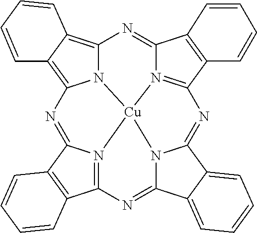 |
Appl. Phys. Lett. 69, 2160 (1996) |
| Starburst triarylamines |
 |
J. Lumin. 72-74, 985 (1997) |
| CFx Fluorohydrocarbon polymer |
|
Appl. Phys. Lett. 78, 673 (2001) |
| Conducting polymers (e.g., PEDOT: PSS, polyaniline, polypthiophene) |
 |
Synth. Met. 87, 171 (1997) WO2007002683 |
| Phosphonic acid and sliane SAMs |
|
US20030162053 |
| Triarylamine or polythiophene polymers with conductivity dopants |    |
EP1725079A1 |
| Arylamines complexed with metal oxides such as molybdenum and tungsten oxides |
 |
SID Symposium Digest, 37, 923 (2006) WO2009018009 |
| p-type semiconducting organic complexes |
 |
US20020158242 |
| Metal organometallic complexes |
 |
US20060240279 |
| Cross-linkable compounds |
 |
US20080220265 |
| Hole transporting materials |
| Triarylamines (e.g., TPD, α-NPD) |
 |
Appl. Phys. Lett. 51, 913 (1987) |
 |
U.S. Pat. No. 5,061,569 | |
 |
EP650955 | |
 |
J. Mater. Chem. 3, 319 (1993) | |
 |
Appl. Phys. Lett. 90, 183503 (2007) | |
 |
Appl. Phys. Lett. 90, 183503 (2007) | |
| Triaylamine on spirofluorene core |
 |
Synth. Met. 91, 209 (1997) |
| Arylamine carbazole compounds |
 |
Adv. Mater. 6, 677 (1994), US20080124572 |
| Triarylamine with (di)benzothiophene/ (di)benzofuran |
 |
US20070278938, US20080106190 |
| Indolocarbazoles |
 |
Synth. Met. 111, 421 (2000) |
| Isoindole compounds |
 |
Chem. Mater. 15, 3148 (2003) |
| Metal carbene complexes |
 |
US20080018221 |
| Phosphorescent OLED host materials |
| Red hosts |
| Arylcarbazoles |
 |
Appl. Phys. Lett. 78, 1622 (2001) |
| Metal 8- hydroxyquinolates (e.g., Alq3, BAlq) |
 |
Nature 395, 151 (1998) |
 |
US20060202194 | |
 |
WO2005014551 | |
 |
WO2006072002 | |
| Metal phenoxybenzothiazole compounds |
 |
Appl. Phys. Lett. 90, 123509 (2007) |
| Conjugated oligomers and polymers (e.g., polyfluorene) |
 |
Org. Electron. 1, 15 (2000) |
| Aromatic fused rings |
 |
WO2009066779, WO2009066778, WO2009063833, US20090045731, US20090045730, WO2009008311, US20090008605, US20090009065 |
| Zinc complexes |
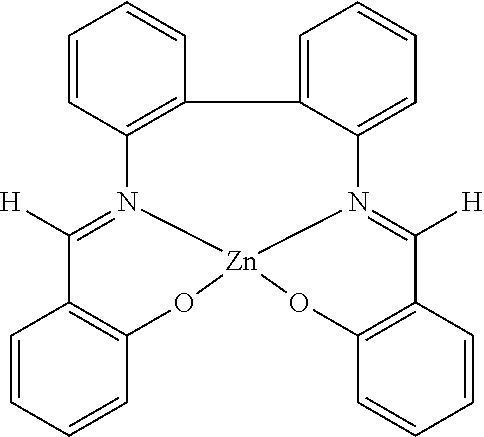 |
WO2009062578 |
| Green hosts |
| Arylcarbazoles |
 |
Appl. Phys. Lett. 78, 1622 (2001) |
 |
US20030175553 | |
 |
WO2001039234 | |
| Aryltriphenylene compounds |
 |
US20060280965 |
 |
US20060280965 | |
 |
WO2009021126 | |
| Donor acceptor type molecules |
 |
WO2008056746 |
| Aza-carbazole/ DBT/DBF |
 |
JP2008074939 |
| Polymers (e.g., PVK) |
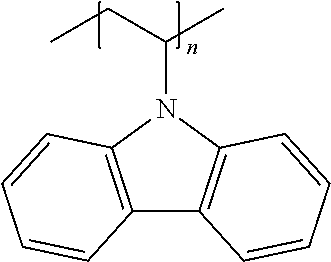 |
Appl. Phys. Lett. 77, 2280 (2000) |
| Spirofluorene compounds |
 |
WO2004093207 |
| Metal phenoxybenzooxazole compounds |
 |
WO2005089025 |
 |
WO2006132173 | |
 |
JP200511610 | |
| Spirofluorene- carbazole compounds |
 |
JP2007254297 |
 |
JP2007254297 | |
| Indolocabazoles |
 |
WO2007063796 |
 |
WO2007063754 | |
| 5-member ring electron deficient heterocycles (e.g., triazole, oxadiazole) |
 |
J. Appl. Phys. 90, 5048 (2001) |
 |
WO2004107822 | |
| Tetraphenylene complexes |
 |
US20050112407 |
| Metal phenoxypyridine compounds |
 |
WO2005030900 |
| Metal coordination complexes (e.g., Zn, Al with N{circumflex over ( )}N ligands) |
 |
US20040137268, US20040137267 |
| Blue Hosts |
| Arylcarbazoles |
 |
Appl. Phys. Lett, 82, 2422 (2003) |
 |
US20070190359 | |
| Dibenzothiophene/ Dibenzofuran- carbazole compounds |
 |
WO2006114966, US20090167162 |
 |
US20090167162 | |
 |
WO2009086028 | |
 |
US20090030202, US20090017330 | |
| Silicon aryl compounds |
 |
US20050238919 |
 |
WO2009003898 | |
| Silicon/Germanium aryl compounds |
 |
EP2034538A |
| Aryl benzoyl ester |
 |
WO2006100298 |
| High triplet metal organometallic complex |
 |
U.S. Pat. No. 7,154,114 |
| Phosphorescent dopants |
| Red dopants |
| Heavy metal porphyrins (e.g., PtOEP) |
 |
Nature 395, 151 (1998) |
| Iridium (III) organometallic complexes |
 |
Appl. Phys. Lett. 78, 1622 (2001) |
 |
US2006835469 | |
 |
US2006835469 | |
 |
US20060202194 | |
 |
US20060202194 | |
 |
US20070087321 | |
 |
US20070087321 | |
 |
Adv. Mater. 19, 739 (2007) | |
 |
WO2009100991 | |
 |
WO2008101842 | |
| Platinum (II) organometallic complexes |
 |
WO2003040257 |
| Osminum (III) complexes |
 |
Chem. Mater. 17, 3532 (2005) |
| Ruthenium (II) complexes |
 |
Adv. Mater. 17, 1059 (2005) |
| Rhenium (I), (II), and (III) complexes |
 |
US20050244673 |
| Green dopants |
| Iridium (III) organometallic complexes |
 |
Inorg. Chem. 40, 1704 (2001) |
| and its derivatives | ||
 |
US20020034656 | |
 |
U.S. Pat. No. 7,332,232 | |
 |
US20090108737 | |
 |
US20090039776 | |
 |
U.S. Pat. No. 6,921,915 | |
 |
U.S. Pat. No. 6,687,266 | |
 |
Chem. Mater. 16, 2480 (2004) | |
 |
US20070190359 | |
 |
US20060008670 JP2007123392 | |
 |
Adv. Mater. 16, 2003 (2004) | |
 |
Angew. Chem. Int. Ed. 2006, 45, 7800 | |
 |
WO2009050290 | |
 |
US20090165846 | |
 |
US20080015355 | |
| Monomer for polymeric metal organometallic compounds |
 |
U.S. Pat. No. 7,250,226, U.S. Pat. No. 7,396,598 |
| Pt (II) organometallic complexes, including polydentated ligands |
 |
Appl. Phys. Lett. 86, 153505 (2005) |
 |
Appl. Phys. Lett. 86, 153505 (2005) | |
 |
Chem. Lett. 34, 592 (2005) | |
 |
WO2002015645 | |
 |
US20060263635 | |
| Cu complexes |
 |
WO2009000673 |
| Gold complexes |
 |
Chem. Commun. 2906 (2005) |
| Rhenium (III) complexes |
 |
Inorg. Chem. 42, 1248 (2003) |
| Deuterated organometallic complexes |
 |
US20030138657 |
| Organometallic complexes with two or more metal centers |
 |
US20030152802 |
 |
U.S. Pat. No. 7,090,928 | |
| Blue dopants |
| Iridium (III) organometallic complexes |
 |
WO2002002714 |
 |
WO2006009024 | |
 |
US20060251923 | |
 |
U.S. Pat. No. 7,393,599, WO2006056418, US20050260441, WO2005019373 | |
 |
U.S. Pat. No. 7,534,505 | |
 |
U.S. Pat. No. 7,445,855 | |
 |
US20070190359, US20080297033 | |
 |
U.S. Pat. No. 7,338,722 | |
 |
US20020134984 | |
 |
Angew. Chem. Int. Ed. 47, 1 (2008) | |
 |
Chem. Mater. 18, 5119 (2006) | |
 |
Inorg. Chem. 46, 4308 (2007) | |
 |
WO2005123873 | |
 |
WO2005123873 | |
 |
WO2007004380 | |
 |
WO2006082742 | |
| Osmium (II) complexes |
 |
U.S. Pat. No. 7,279,704 |
 |
Organometallics 23, 3745 (2004) | |
| Gold complexes |
 |
Appl. Phys. Lett. 74, 1361 (1999) |
| Platinum (II) complexes |
 |
WO2006098120, WO2006103874 |
| Exciton/hole blocking layer materials |
| Bathocuprine compounds (e.g., BCP, BPhen) |
 |
Appl. Phys. Lett. 75, 4 (1999) |
 |
Appl. Phys. Lett. 79, 449 (2001) | |
| Metal 8- hydroxyquinolates (e.g., BAlq) |
 |
Appl. Phys. Lett. 81, 162 (2002) |
| 5-member ring electron deficient heterocycles such as triazole, oxadiazole, imidazole, benzoimidazole |
 |
Appl. Phys. Lett. 81, 162 (2002) |
| Triphenylene compounds |
 |
US20050025993 |
| Fluorinated aromatic compounds |
 |
Appl. Phys. Lett. 79, 156 (2001) |
| Phenothiazine-S- oxide |
 |
WO2008132085 |
| Electron transporting materials |
| Anthracene- benzoimidazole compounds |
 |
WO2003060956 |
 |
US20090179554 | |
| Aza triphenylene derivatives |
 |
US20090115316 |
| Anthracene- benzothiazole compounds |
 |
Appl. Phys. Lett. 89, 063504 (2006) |
| Metal 8- hydroxyquinolates (e.g., Alq3, Zrq4) |
 |
Appl. Phys. Lett. 51, 913 (1987) U.S. Pat. No. 7,230,107 |
| Metal hydroxy- benoquinolates |
 |
Chem. Lett. 5, 905 (1993) |
| Bathocuprine compounds such as BCP, BPhen, etc |
 |
Appl. Phys. Lett. 91, 263503 (2007) |
 |
Appl. Phys. Lett. 79, 449 (2001) | |
| 5-member ring electron deficient heterocycles (e.g., triazole, oxadiazole, imidazole, benzoimidazole) |
 |
Appl. Phys. Lett. 74, 865 (1999) |
 |
Appl. Phys. Lett. 55, 1489 (1989) | |
 |
Jpn. J. Apply. Phys. 32, L917 (1993) | |
| Silole compounds |
 |
Org. Electron. 4, 113 (2003) |
| Arylborane compounds |
 |
J. Am. Chem. Soc. 120, 9714 (1998) |
| Fluorinated aromatic compounds |
 |
J. Am. Chem. Soc. 122, 1832 (2000) |
| Fullerene (e.g., C60) |
 |
US20090101870 |
| Triazine complexes |
 |
US20040036077 |
| Zn (N{circumflex over ( )}N) complexes |
 |
U.S. Pat. No. 6,528,187 |
Claims (25)
Priority Applications (1)
| Application Number | Priority Date | Filing Date | Title |
|---|---|---|---|
| US13/788,321 US9397312B2 (en) | 2011-05-11 | 2013-03-07 | Process for fabricating metal bus lines for OLED lighting panels |
Applications Claiming Priority (2)
| Application Number | Priority Date | Filing Date | Title |
|---|---|---|---|
| US13/105,770 US8432095B2 (en) | 2011-05-11 | 2011-05-11 | Process for fabricating metal bus lines for OLED lighting panels |
| US13/788,321 US9397312B2 (en) | 2011-05-11 | 2013-03-07 | Process for fabricating metal bus lines for OLED lighting panels |
Related Parent Applications (1)
| Application Number | Title | Priority Date | Filing Date |
|---|---|---|---|
| US13/105,770 Division US8432095B2 (en) | 2011-05-11 | 2011-05-11 | Process for fabricating metal bus lines for OLED lighting panels |
Publications (2)
| Publication Number | Publication Date |
|---|---|
| US20140091282A1 US20140091282A1 (en) | 2014-04-03 |
| US9397312B2 true US9397312B2 (en) | 2016-07-19 |
Family
ID=46246177
Family Applications (2)
| Application Number | Title | Priority Date | Filing Date |
|---|---|---|---|
| US13/105,770 Active US8432095B2 (en) | 2011-05-11 | 2011-05-11 | Process for fabricating metal bus lines for OLED lighting panels |
| US13/788,321 Active 2031-07-21 US9397312B2 (en) | 2011-05-11 | 2013-03-07 | Process for fabricating metal bus lines for OLED lighting panels |
Family Applications Before (1)
| Application Number | Title | Priority Date | Filing Date |
|---|---|---|---|
| US13/105,770 Active US8432095B2 (en) | 2011-05-11 | 2011-05-11 | Process for fabricating metal bus lines for OLED lighting panels |
Country Status (3)
| Country | Link |
|---|---|
| US (2) | US8432095B2 (en) |
| TW (2) | TWI639263B (en) |
| WO (1) | WO2012170145A1 (en) |
Cited By (1)
| Publication number | Priority date | Publication date | Assignee | Title |
|---|---|---|---|---|
| US11359770B2 (en) | 2018-06-06 | 2022-06-14 | Beijing Summer Sprout Technology Co. Ltd. | High-yield low-cost large-area flexible OLED lighting module |
Families Citing this family (9)
| Publication number | Priority date | Publication date | Assignee | Title |
|---|---|---|---|---|
| US8564192B2 (en) | 2011-05-11 | 2013-10-22 | Universal Display Corporation | Process for fabricating OLED lighting panels |
| US8981640B2 (en) | 2011-05-11 | 2015-03-17 | Universal Display Corporation | Simplified patterned light panel |
| WO2014039687A1 (en) | 2012-09-06 | 2014-03-13 | Plextronics, Inc. | Electroluminescent devices comprising insulator-free metal grids |
| WO2014187896A1 (en) * | 2013-05-23 | 2014-11-27 | Koninklijke Philips N.V. | Light-emitting device with alternating arrangement of anode pads and cathode pads |
| US10749123B2 (en) | 2014-03-27 | 2020-08-18 | Universal Display Corporation | Impact resistant OLED devices |
| US10910590B2 (en) | 2014-03-27 | 2021-02-02 | Universal Display Corporation | Hermetically sealed isolated OLED pixels |
| CN104062842B (en) * | 2014-06-30 | 2019-02-15 | 上海天马有机发光显示技术有限公司 | A kind of mask plate and its manufacturing method, process unit |
| KR102369676B1 (en) | 2017-04-10 | 2022-03-04 | 삼성디스플레이 주식회사 | Apparatus and method for manufacturing a display apparatus |
| CN107123666A (en) * | 2017-05-27 | 2017-09-01 | 上海天马微电子有限公司 | Display panel and display device |
Citations (135)
| Publication number | Priority date | Publication date | Assignee | Title |
|---|---|---|---|---|
| US4469719A (en) | 1981-12-21 | 1984-09-04 | Applied Magnetics-Magnetic Head Divison Corporation | Method for controlling the edge gradient of a layer of deposition material |
| US4769292A (en) | 1987-03-02 | 1988-09-06 | Eastman Kodak Company | Electroluminescent device with modified thin film luminescent zone |
| US5061569A (en) | 1990-07-26 | 1991-10-29 | Eastman Kodak Company | Electroluminescent device with organic electroluminescent medium |
| US5247190A (en) | 1989-04-20 | 1993-09-21 | Cambridge Research And Innovation Limited | Electroluminescent devices |
| EP0650955A1 (en) | 1993-11-01 | 1995-05-03 | Hodogaya Chemical Co., Ltd. | Amine compound and electro-luminescence device comprising same |
| US5703436A (en) | 1994-12-13 | 1997-12-30 | The Trustees Of Princeton University | Transparent contacts for organic devices |
| US5707745A (en) | 1994-12-13 | 1998-01-13 | The Trustees Of Princeton University | Multicolor organic light emitting devices |
| US5834893A (en) | 1996-12-23 | 1998-11-10 | The Trustees Of Princeton University | High efficiency organic light emitting devices with light directing structures |
| US5844363A (en) | 1997-01-23 | 1998-12-01 | The Trustees Of Princeton Univ. | Vacuum deposited, non-polymeric flexible organic light emitting devices |
| US6013982A (en) | 1996-12-23 | 2000-01-11 | The Trustees Of Princeton University | Multicolor display devices |
| US6087196A (en) | 1998-01-30 | 2000-07-11 | The Trustees Of Princeton University | Fabrication of organic semiconductor devices using ink jet printing |
| US6091195A (en) | 1997-02-03 | 2000-07-18 | The Trustees Of Princeton University | Displays having mesa pixel configuration |
| US6097147A (en) | 1998-09-14 | 2000-08-01 | The Trustees Of Princeton University | Structure for high efficiency electroluminescent device |
| WO2001039234A2 (en) | 1999-11-24 | 2001-05-31 | The Trustees Of Princeton University | Organic light emitting diode having a blue phosphorescent molecule as an emitter |
| US6294398B1 (en) | 1999-11-23 | 2001-09-25 | The Trustees Of Princeton University | Method for patterning devices |
| US6303238B1 (en) | 1997-12-01 | 2001-10-16 | The Trustees Of Princeton University | OLEDs doped with phosphorescent compounds |
| US6337102B1 (en) | 1997-11-17 | 2002-01-08 | The Trustees Of Princeton University | Low pressure vapor phase deposition of organic thin films |
| WO2002002714A2 (en) | 2000-06-30 | 2002-01-10 | E.I. Du Pont De Nemours And Company | Electroluminescent iridium compounds with fluorinated phenylpyridines, phenylpyrimidines, and phenylquinolines and devices made with such compounds |
| WO2002015645A1 (en) | 2000-08-11 | 2002-02-21 | The Trustees Of Princeton University | Organometallic compounds and emission-shifting organic electrophosphorescence |
| US20020034656A1 (en) | 1998-09-14 | 2002-03-21 | Thompson Mark E. | Organometallic complexes as phosphorescent emitters in organic LEDs |
| US6403392B1 (en) | 1998-10-30 | 2002-06-11 | The Trustees Of Princeton University | Method for patterning devices |
| US20020134984A1 (en) | 2001-02-01 | 2002-09-26 | Fuji Photo Film Co., Ltd. | Transition metal complex and light-emitting device |
| US20020158242A1 (en) | 1999-12-31 | 2002-10-31 | Se-Hwan Son | Electronic device comprising organic compound having p-type semiconducting characteristics |
| US20030006697A1 (en) | 2001-07-09 | 2003-01-09 | Weaver Michael S. | Method for patterning devices |
| US6528187B1 (en) | 1998-09-08 | 2003-03-04 | Fuji Photo Film Co., Ltd. | Material for luminescence element and luminescence element using the same |
| WO2003040257A1 (en) | 2001-11-07 | 2003-05-15 | E. I. Du Pont De Nemours And Company | Electroluminescent platinum compounds and devices made with such compounds |
| US20030138657A1 (en) | 2000-12-07 | 2003-07-24 | Canon Kabushiki Kaisha | Deuterated semi-conducting organic compounds used for opto-electronic devices |
| EP1331666A2 (en) | 2002-01-24 | 2003-07-30 | Semiconductor Energy Laboratory Co., Ltd. | Light emitting device and method of manufacturing the same |
| US20030152802A1 (en) | 2001-06-19 | 2003-08-14 | Akira Tsuboyama | Metal coordination compound and organic liminescence device |
| US20030162053A1 (en) | 1996-06-25 | 2003-08-28 | Marks Tobin J. | Organic light - emitting diodes and methods for assembly and enhanced charge injection |
| US20030175553A1 (en) | 2001-12-28 | 2003-09-18 | Thompson Mark E. | White light emitting oleds from combined monomer and aggregate emission |
| US6626721B1 (en) | 2000-09-22 | 2003-09-30 | Eastman Kodak Company | Organic electroluminescent device with supplemental cathode bus conductor |
| WO2003060956A3 (en) | 2002-01-18 | 2003-11-13 | Lg Chemical Ltd | New material for transporting electrons and organic electroluminescent display using the same |
| US20030230980A1 (en) | 2002-06-18 | 2003-12-18 | Forrest Stephen R | Very low voltage, high efficiency phosphorescent oled in a p-i-n structure |
| US6687266B1 (en) | 2002-11-08 | 2004-02-03 | Universal Display Corporation | Organic light emitting materials and devices |
| US20040036077A1 (en) | 2002-08-22 | 2004-02-26 | Fuji Photo Film Co., Ltd. | Light emitting element |
| US20040137267A1 (en) | 2002-12-27 | 2004-07-15 | Fuji Photo Film Co., Ltd. | Organic electroluminescent device |
| US20040137268A1 (en) | 2002-12-27 | 2004-07-15 | Fuji Photo Film Co., Ltd. | Organic electroluminescent device |
| US20040174116A1 (en) | 2001-08-20 | 2004-09-09 | Lu Min-Hao Michael | Transparent electrodes |
| WO2004107822A1 (en) | 2003-05-29 | 2004-12-09 | Nippon Steel Chemical Co., Ltd. | Organic electroluminescent element |
| US20040253756A1 (en) | 2003-06-16 | 2004-12-16 | Eastman Kodak Company | Method of making a top-emitting OLED device having improved power distribution |
| US6835469B2 (en) | 2001-10-17 | 2004-12-28 | The University Of Southern California | Phosphorescent compounds and devices comprising the same |
| JP2005011610A (en) | 2003-06-18 | 2005-01-13 | Nippon Steel Chem Co Ltd | Organic electroluminescent element |
| US20050025993A1 (en) | 2003-07-25 | 2005-02-03 | Thompson Mark E. | Materials and structures for enhancing the performance of organic light emitting devices |
| WO2005014551A1 (en) | 2003-08-07 | 2005-02-17 | Nippon Steel Chemical Co., Ltd. | Aluminum chelate compelx for organic el material |
| WO2005019373A2 (en) | 2003-08-19 | 2005-03-03 | Basf Aktiengesellschaft | Transition metal complexes comprising carbene ligands serving as emitters for organic light-emitting diodes (oled's) |
| WO2005030900A1 (en) | 2003-09-25 | 2005-04-07 | Nippon Steel Chemical Co., Ltd. | Organic electroluminescent device |
| US6891327B2 (en) * | 2001-04-26 | 2005-05-10 | Koninklijke Philips Electronics N.V. | Organic electroluminescent device and a method of manufacturing thereof |
| US20050112407A1 (en) | 2003-11-21 | 2005-05-26 | Fuji Photo Film Co., Ltd. | Organic electroluminescent device |
| WO2004093207A3 (en) | 2003-04-15 | 2005-06-09 | Covion Organic Semiconductors | Mixtures of matrix materials and organic semiconductors capable of emission, use of the same and electronic components containing said mixtures |
| US6921915B2 (en) | 2001-03-08 | 2005-07-26 | Canon Kabushiki Kaisha | Metal coordination compound, luminescence device and display apparatus |
| WO2005089025A1 (en) | 2004-03-15 | 2005-09-22 | Nippon Steel Chemical Co., Ltd. | Organic electroluminescent device |
| US20050238919A1 (en) | 2004-04-23 | 2005-10-27 | Fuji Photo Film Co., Ltd. | Organic electroluminescent device |
| US20050244673A1 (en) | 2002-08-27 | 2005-11-03 | Fujitsu Limited | Organometallic complex, organic EL element and organic EL display |
| US20050260441A1 (en) | 2004-05-18 | 2005-11-24 | Thompson Mark E | Luminescent compounds with carbene ligands |
| US20050260449A1 (en) | 2004-05-18 | 2005-11-24 | Robert Walters | Complexes with tridentate ligands |
| WO2005123873A1 (en) | 2004-06-17 | 2005-12-29 | Konica Minolta Holdings, Inc. | Organic electroluminescent device material, organic electroluminescent device, display and illuminating device |
| US20060008670A1 (en) | 2004-07-06 | 2006-01-12 | Chun Lin | Organic light emitting materials and devices |
| WO2006009024A1 (en) | 2004-07-23 | 2006-01-26 | Konica Minolta Holdings, Inc. | Organic electroluminescent device, display and illuminating device |
| JP2006147190A (en) | 2004-11-16 | 2006-06-08 | Dainippon Printing Co Ltd | Light emission display panel and production method therefor |
| US7087321B2 (en) | 2003-04-22 | 2006-08-08 | Universal Display Corporation | Organic light emitting devices having reduced pixel shrinkage |
| WO2006082742A1 (en) | 2005-02-04 | 2006-08-10 | Konica Minolta Holdings, Inc. | Organic electroluminescent device material, organic electroluminescent device, display and illuminating device |
| US7090928B2 (en) | 2003-04-01 | 2006-08-15 | The University Of Southern California | Binuclear compounds |
| US20060202194A1 (en) | 2005-03-08 | 2006-09-14 | Jeong Hyun C | Red phosphorescene compounds and organic electroluminescence device using the same |
| WO2006098120A1 (en) | 2005-03-16 | 2006-09-21 | Konica Minolta Holdings, Inc. | Organic electroluminescent device material and organic electroluminescent device |
| WO2006100298A1 (en) | 2005-03-24 | 2006-09-28 | Basf Aktiengesellschaft | Use of compounds containing aromatic or heteroaromatic rings linked via carbonyl group-containing groups, for use as matrix materials in organic light-emitting diodes |
| WO2006103874A1 (en) | 2005-03-29 | 2006-10-05 | Konica Minolta Holdings, Inc. | Organic electroluminescent device material, organic electroluminescent device, display and illuminating device |
| US20060240279A1 (en) | 2005-04-21 | 2006-10-26 | Vadim Adamovich | Non-blocked phosphorescent OLEDs |
| WO2006114966A1 (en) | 2005-04-18 | 2006-11-02 | Konica Minolta Holdings, Inc. | Organic electroluminescent device, display and illuminating device |
| US20060251923A1 (en) | 2005-05-06 | 2006-11-09 | Chun Lin | Stability OLED materials and devices |
| EP1725079A1 (en) | 2004-03-11 | 2006-11-22 | Mitsubishi Chemical Corporation | Composition for charge-transporting film and ion compound, charge-transporting film and organic electroluminescent device using same, and method for manufacturing organic electroluminescent device and method for producing charge-transporting film |
| US20060263635A1 (en) | 2005-05-06 | 2006-11-23 | Fuji Photo Film Co., Ltd. | Organic electroluminescent device |
| US20060280965A1 (en) | 2005-05-31 | 2006-12-14 | Raymond Kwong | Triphenylene hosts in phosphorescent light emitting diodes |
| WO2006132173A1 (en) | 2005-06-07 | 2006-12-14 | Nippon Steel Chemical Co., Ltd. | Organic metal complex and organic electroluminescent device using same |
| US7154114B2 (en) | 2004-05-18 | 2006-12-26 | Universal Display Corporation | Cyclometallated iridium carbene complexes for use as hosts |
| WO2007004380A1 (en) | 2005-07-01 | 2007-01-11 | Konica Minolta Holdings, Inc. | Organic electroluminescent element material, organic electroluminescent element, display device, and lighting equipment |
| WO2006056418A8 (en) | 2004-11-25 | 2007-03-01 | Basf Ag | Use of transition metal carbene complexes in organic light-emitting diodes (oleds) |
| WO2006072002A3 (en) | 2004-12-30 | 2007-03-01 | Du Pont | Organometallic complexes |
| JP2007123392A (en) | 2005-10-26 | 2007-05-17 | Konica Minolta Holdings Inc | Organic electroluminescence device, display device and lighting device |
| WO2007063796A1 (en) | 2005-12-01 | 2007-06-07 | Nippon Steel Chemical Co., Ltd. | Organic electroluminescent device |
| WO2007063754A1 (en) | 2005-12-01 | 2007-06-07 | Nippon Steel Chemical Co., Ltd. | Compound for organic electroluminescent element and organic electroluminescent element |
| US7250226B2 (en) | 2001-08-31 | 2007-07-31 | Nippon Hoso Kyokai | Phosphorescent compound, a phosphorescent composition and an organic light-emitting device |
| US20070190359A1 (en) | 2006-02-10 | 2007-08-16 | Knowles David B | Metal complexes of cyclometallated imidazo[1,2-ƒ]phenanthridine and diimidazo[1,2-a:1',2'-c]quinazoline ligands and isoelectronic and benzannulated analogs thereof |
| WO2007002683A3 (en) | 2005-06-27 | 2007-09-20 | Du Pont | Electrically conductive polymer compositions |
| JP2007254297A (en) | 2006-03-20 | 2007-10-04 | Nippon Steel Chem Co Ltd | Compound of light-emitting layer and organic electroluminescent device |
| US20070278938A1 (en) | 2006-04-26 | 2007-12-06 | Idemitsu Kosan Co., Ltd. | Aromatic amine derivative and electroluminescence device using the same |
| US20080015355A1 (en) | 2004-06-28 | 2008-01-17 | Thomas Schafer | Electroluminescent Metal Complexes With Triazoles And Benzotriazoles |
| US7332232B2 (en) | 2004-02-03 | 2008-02-19 | Universal Display Corporation | OLEDs utilizing multidentate ligand systems |
| US7338722B2 (en) | 2003-03-24 | 2008-03-04 | The University Of Southern California | Phenyl and fluorenyl substituted phenyl-pyrazole complexes of Ir |
| JP2008074939A (en) | 2006-09-21 | 2008-04-03 | Konica Minolta Holdings Inc | Organic electroluminescence element material, organic electroluminescence element, display device and illumination device |
| US20080106190A1 (en) | 2006-08-23 | 2008-05-08 | Idemitsu Kosan Co., Ltd. | Aromatic amine derivatives and organic electroluminescent device using same |
| WO2008056746A1 (en) | 2006-11-09 | 2008-05-15 | Nippon Steel Chemical Co., Ltd. | Compound for organic electroluminescent device and organic electroluminescent device |
| US20080124572A1 (en) | 2006-11-24 | 2008-05-29 | Idemitsu Kosan Co., Ltd. | Aromatic amine derivative and organic electroluminescence device using the same |
| US7393599B2 (en) | 2004-05-18 | 2008-07-01 | The University Of Southern California | Luminescent compounds with carbene ligands |
| US7396598B2 (en) | 2001-06-20 | 2008-07-08 | Showa Denko K.K. | Light emitting material and organic light-emitting device |
| WO2008101842A1 (en) | 2007-02-23 | 2008-08-28 | Basf Se | Electroluminescent metal complexes with benzotriazoles |
| US20080220265A1 (en) | 2006-12-08 | 2008-09-11 | Universal Display Corporation | Cross-linkable Iridium Complexes and Organic Light-Emitting Devices Using the Same |
| TWI300996B (en) | 2006-04-05 | 2008-09-11 | Daewoo Electronics Corp | Organic electroluminescence device and method for manufacturing same |
| US7431968B1 (en) | 2001-09-04 | 2008-10-07 | The Trustees Of Princeton University | Process and apparatus for organic vapor jet deposition |
| US7445855B2 (en) | 2004-05-18 | 2008-11-04 | The University Of Southern California | Cationic metal-carbene complexes |
| WO2008132085A1 (en) | 2007-04-26 | 2008-11-06 | Basf Se | Silanes containing phenothiazine-s-oxide or phenothiazine-s,s-dioxide groups and the use thereof in oleds |
| US20080297033A1 (en) | 2006-02-10 | 2008-12-04 | Knowles David B | Blue phosphorescent imidazophenanthridine materials |
| WO2009000673A2 (en) | 2007-06-22 | 2008-12-31 | Basf Se | Light emitting cu(i) complexes |
| US20090008605A1 (en) | 2007-07-07 | 2009-01-08 | Idemitsu Kosan Co., Ltd. | Naphthalene derivative, material for organic electroluminescence device, and organic electroluminescence device using the same |
| US20090009065A1 (en) | 2007-07-07 | 2009-01-08 | Idemitsu Kosan Co., Ltd. | Organic electroluminescence device and material for organic electroluminescence device |
| WO2009003898A1 (en) | 2007-07-05 | 2009-01-08 | Basf Se | Organic light-emitting diodes containing carbene transition metal complex emitters and at least one compound selected from disilylcarbazoles, disilyldibenzofurans, disilyldibenzothiophenes, disilyldibenzophospholes, disilyldibenzothiophene s-oxides and disilyldibenzothiophene s,s-dioxides |
| US20090017330A1 (en) | 2007-07-10 | 2009-01-15 | Idemitsu Kosan Co., Ltd. | Material for organic electroluminescence device and organic electroluminescence device utilizing the same |
| WO2009008311A1 (en) | 2007-07-07 | 2009-01-15 | Idemitsu Kosan Co., Ltd. | Chrysene derivative and organic electroluminescent device using the same |
| US20090030202A1 (en) | 2007-07-10 | 2009-01-29 | Idemitsu Kosan Co., Ltd. | Material for organic electroluminescent element and organic electroluminescent element employing the same |
| WO2009018009A1 (en) | 2007-07-27 | 2009-02-05 | E. I. Du Pont De Nemours And Company | Aqueous dispersions of electrically conducting polymers containing inorganic nanoparticles |
| WO2009021126A2 (en) | 2007-08-08 | 2009-02-12 | Universal Display Corporation | Benzo-fused thiophene or benzo-fused furan compounds comprising a triphenylene group |
| US20090039776A1 (en) | 2007-08-09 | 2009-02-12 | Canon Kabushiki Kaisha | Organometallic complex and organic light-emitting element using same |
| US20090045731A1 (en) | 2007-07-07 | 2009-02-19 | Idemitsu Kosan Co., Ltd. | Organic electroluminescence device and material for organic electroluminescence device |
| US20090045730A1 (en) | 2007-07-07 | 2009-02-19 | Idemitsu Kosan Co., Ltd. | Organic electroluminescence device and material for organic electroluminescence device |
| US20090061724A1 (en) | 2007-09-04 | 2009-03-05 | Cok Ronald S | Method of making a top-emitting oled device having improved power distribution |
| EP2034538A1 (en) | 2006-06-02 | 2009-03-11 | Idemitsu Kosan Co., Ltd. | Material for organic electroluminescence element, and organic electroluminescence element using the material |
| US20090101870A1 (en) | 2007-10-22 | 2009-04-23 | E. I. Du Pont De Nemours And Company | Electron transport bi-layers and devices made with such bi-layers |
| WO2009050290A1 (en) | 2007-10-17 | 2009-04-23 | Basf Se | Transition metal complexes having bridged carbene ligands and the use thereof in oleds |
| US20090108737A1 (en) | 2006-12-08 | 2009-04-30 | Raymond Kwong | Light-emitting organometallic complexes |
| US20090115316A1 (en) | 2007-11-02 | 2009-05-07 | Shiying Zheng | Organic electroluminescent device having an azatriphenylene derivative |
| US7534505B2 (en) | 2004-05-18 | 2009-05-19 | The University Of Southern California | Organometallic compounds for use in electroluminescent devices |
| WO2009063833A1 (en) | 2007-11-15 | 2009-05-22 | Idemitsu Kosan Co., Ltd. | Benzochrysene derivative and organic electroluminescent device using the same |
| WO2009062578A1 (en) | 2007-11-12 | 2009-05-22 | Merck Patent Gmbh | Organic electroluminescent devices comprising azomethine-metal complexes |
| WO2009066779A1 (en) | 2007-11-22 | 2009-05-28 | Idemitsu Kosan Co., Ltd. | Organic el element |
| WO2009066778A1 (en) | 2007-11-22 | 2009-05-28 | Idemitsu Kosan Co., Ltd. | Organic el element and solution containing organic el material |
| US20090146557A1 (en) | 2007-12-07 | 2009-06-11 | Seiko Epson Corporation | Light-emitting device, electronic apparatus, and film-forming method |
| US20090165846A1 (en) | 2005-09-07 | 2009-07-02 | Universitaet Braunschweig | Triplet emitter having condensed five-membered rings |
| US20090167162A1 (en) | 2007-12-28 | 2009-07-02 | Universal Display Corporation | Dibenzothiophene-containing materials in phosphorescent light emitting diodes |
| WO2009086028A2 (en) | 2007-12-28 | 2009-07-09 | Universal Display Corporation | Carbazole-containing materials in phosphorescent light emitting diodes |
| US20090179554A1 (en) | 2006-05-11 | 2009-07-16 | Hitoshi Kuma | Organic electroluminescent device |
| US7576496B2 (en) | 1999-12-22 | 2009-08-18 | General Electric Company | AC powered OLED device |
| WO2009100991A1 (en) | 2008-02-12 | 2009-08-20 | Basf Se | Electroluminescent metal complexes with dibenzo[f,h]quinoxalines |
| KR20090116551A (en) | 2008-05-07 | 2009-11-11 | 엘지전자 주식회사 | Display panel |
| WO2010038181A1 (en) | 2008-10-02 | 2010-04-08 | Philips Intellectual Property & Standards Gmbh | Oled device with covered shunt line |
| JP2010080310A (en) | 2008-09-26 | 2010-04-08 | Dainippon Printing Co Ltd | Organic electroluminescence element, and method for manufacturing the same |
Family Cites Families (1)
| Publication number | Priority date | Publication date | Assignee | Title |
|---|---|---|---|---|
| US7034470B2 (en) | 2002-08-07 | 2006-04-25 | Eastman Kodak Company | Serially connecting OLED devices for area illumination |
-
2011
- 2011-05-11 US US13/105,770 patent/US8432095B2/en active Active
-
2012
- 2012-05-10 TW TW101116731A patent/TWI639263B/en active
- 2012-05-10 TW TW106118554A patent/TW201803183A/en unknown
- 2012-05-10 WO PCT/US2012/037378 patent/WO2012170145A1/en active Application Filing
-
2013
- 2013-03-07 US US13/788,321 patent/US9397312B2/en active Active
Patent Citations (140)
| Publication number | Priority date | Publication date | Assignee | Title |
|---|---|---|---|---|
| US4469719A (en) | 1981-12-21 | 1984-09-04 | Applied Magnetics-Magnetic Head Divison Corporation | Method for controlling the edge gradient of a layer of deposition material |
| US4769292A (en) | 1987-03-02 | 1988-09-06 | Eastman Kodak Company | Electroluminescent device with modified thin film luminescent zone |
| US5247190A (en) | 1989-04-20 | 1993-09-21 | Cambridge Research And Innovation Limited | Electroluminescent devices |
| US5061569A (en) | 1990-07-26 | 1991-10-29 | Eastman Kodak Company | Electroluminescent device with organic electroluminescent medium |
| EP0650955A1 (en) | 1993-11-01 | 1995-05-03 | Hodogaya Chemical Co., Ltd. | Amine compound and electro-luminescence device comprising same |
| US5703436A (en) | 1994-12-13 | 1997-12-30 | The Trustees Of Princeton University | Transparent contacts for organic devices |
| US5707745A (en) | 1994-12-13 | 1998-01-13 | The Trustees Of Princeton University | Multicolor organic light emitting devices |
| US20030162053A1 (en) | 1996-06-25 | 2003-08-28 | Marks Tobin J. | Organic light - emitting diodes and methods for assembly and enhanced charge injection |
| US6013982A (en) | 1996-12-23 | 2000-01-11 | The Trustees Of Princeton University | Multicolor display devices |
| US5834893A (en) | 1996-12-23 | 1998-11-10 | The Trustees Of Princeton University | High efficiency organic light emitting devices with light directing structures |
| US5844363A (en) | 1997-01-23 | 1998-12-01 | The Trustees Of Princeton Univ. | Vacuum deposited, non-polymeric flexible organic light emitting devices |
| US6091195A (en) | 1997-02-03 | 2000-07-18 | The Trustees Of Princeton University | Displays having mesa pixel configuration |
| US6337102B1 (en) | 1997-11-17 | 2002-01-08 | The Trustees Of Princeton University | Low pressure vapor phase deposition of organic thin films |
| US6303238B1 (en) | 1997-12-01 | 2001-10-16 | The Trustees Of Princeton University | OLEDs doped with phosphorescent compounds |
| US6087196A (en) | 1998-01-30 | 2000-07-11 | The Trustees Of Princeton University | Fabrication of organic semiconductor devices using ink jet printing |
| US6528187B1 (en) | 1998-09-08 | 2003-03-04 | Fuji Photo Film Co., Ltd. | Material for luminescence element and luminescence element using the same |
| US6097147A (en) | 1998-09-14 | 2000-08-01 | The Trustees Of Princeton University | Structure for high efficiency electroluminescent device |
| US20020034656A1 (en) | 1998-09-14 | 2002-03-21 | Thompson Mark E. | Organometallic complexes as phosphorescent emitters in organic LEDs |
| US6403392B1 (en) | 1998-10-30 | 2002-06-11 | The Trustees Of Princeton University | Method for patterning devices |
| US6468819B1 (en) | 1999-11-23 | 2002-10-22 | The Trustees Of Princeton University | Method for patterning organic thin film devices using a die |
| US6294398B1 (en) | 1999-11-23 | 2001-09-25 | The Trustees Of Princeton University | Method for patterning devices |
| WO2001039234A2 (en) | 1999-11-24 | 2001-05-31 | The Trustees Of Princeton University | Organic light emitting diode having a blue phosphorescent molecule as an emitter |
| US7576496B2 (en) | 1999-12-22 | 2009-08-18 | General Electric Company | AC powered OLED device |
| US20020158242A1 (en) | 1999-12-31 | 2002-10-31 | Se-Hwan Son | Electronic device comprising organic compound having p-type semiconducting characteristics |
| WO2002002714A2 (en) | 2000-06-30 | 2002-01-10 | E.I. Du Pont De Nemours And Company | Electroluminescent iridium compounds with fluorinated phenylpyridines, phenylpyrimidines, and phenylquinolines and devices made with such compounds |
| WO2002015645A1 (en) | 2000-08-11 | 2002-02-21 | The Trustees Of Princeton University | Organometallic compounds and emission-shifting organic electrophosphorescence |
| US6626721B1 (en) | 2000-09-22 | 2003-09-30 | Eastman Kodak Company | Organic electroluminescent device with supplemental cathode bus conductor |
| US20030138657A1 (en) | 2000-12-07 | 2003-07-24 | Canon Kabushiki Kaisha | Deuterated semi-conducting organic compounds used for opto-electronic devices |
| US20020134984A1 (en) | 2001-02-01 | 2002-09-26 | Fuji Photo Film Co., Ltd. | Transition metal complex and light-emitting device |
| US6921915B2 (en) | 2001-03-08 | 2005-07-26 | Canon Kabushiki Kaisha | Metal coordination compound, luminescence device and display apparatus |
| US6891327B2 (en) * | 2001-04-26 | 2005-05-10 | Koninklijke Philips Electronics N.V. | Organic electroluminescent device and a method of manufacturing thereof |
| US20030152802A1 (en) | 2001-06-19 | 2003-08-14 | Akira Tsuboyama | Metal coordination compound and organic liminescence device |
| US7396598B2 (en) | 2001-06-20 | 2008-07-08 | Showa Denko K.K. | Light emitting material and organic light-emitting device |
| US20030006697A1 (en) | 2001-07-09 | 2003-01-09 | Weaver Michael S. | Method for patterning devices |
| US20040174116A1 (en) | 2001-08-20 | 2004-09-09 | Lu Min-Hao Michael | Transparent electrodes |
| US7250226B2 (en) | 2001-08-31 | 2007-07-31 | Nippon Hoso Kyokai | Phosphorescent compound, a phosphorescent composition and an organic light-emitting device |
| US7431968B1 (en) | 2001-09-04 | 2008-10-07 | The Trustees Of Princeton University | Process and apparatus for organic vapor jet deposition |
| US6835469B2 (en) | 2001-10-17 | 2004-12-28 | The University Of Southern California | Phosphorescent compounds and devices comprising the same |
| WO2003040257A1 (en) | 2001-11-07 | 2003-05-15 | E. I. Du Pont De Nemours And Company | Electroluminescent platinum compounds and devices made with such compounds |
| US20030175553A1 (en) | 2001-12-28 | 2003-09-18 | Thompson Mark E. | White light emitting oleds from combined monomer and aggregate emission |
| WO2003060956A3 (en) | 2002-01-18 | 2003-11-13 | Lg Chemical Ltd | New material for transporting electrons and organic electroluminescent display using the same |
| EP1331666A2 (en) | 2002-01-24 | 2003-07-30 | Semiconductor Energy Laboratory Co., Ltd. | Light emitting device and method of manufacturing the same |
| TWI278255B (en) | 2002-01-24 | 2007-04-01 | Semiconductor Energy Lab | Light emitting device and method of manufacturing the same |
| US20030230980A1 (en) | 2002-06-18 | 2003-12-18 | Forrest Stephen R | Very low voltage, high efficiency phosphorescent oled in a p-i-n structure |
| US20040036077A1 (en) | 2002-08-22 | 2004-02-26 | Fuji Photo Film Co., Ltd. | Light emitting element |
| US20050244673A1 (en) | 2002-08-27 | 2005-11-03 | Fujitsu Limited | Organometallic complex, organic EL element and organic EL display |
| US6687266B1 (en) | 2002-11-08 | 2004-02-03 | Universal Display Corporation | Organic light emitting materials and devices |
| US20040137268A1 (en) | 2002-12-27 | 2004-07-15 | Fuji Photo Film Co., Ltd. | Organic electroluminescent device |
| US20040137267A1 (en) | 2002-12-27 | 2004-07-15 | Fuji Photo Film Co., Ltd. | Organic electroluminescent device |
| US7338722B2 (en) | 2003-03-24 | 2008-03-04 | The University Of Southern California | Phenyl and fluorenyl substituted phenyl-pyrazole complexes of Ir |
| US7090928B2 (en) | 2003-04-01 | 2006-08-15 | The University Of Southern California | Binuclear compounds |
| WO2004093207A3 (en) | 2003-04-15 | 2005-06-09 | Covion Organic Semiconductors | Mixtures of matrix materials and organic semiconductors capable of emission, use of the same and electronic components containing said mixtures |
| US7087321B2 (en) | 2003-04-22 | 2006-08-08 | Universal Display Corporation | Organic light emitting devices having reduced pixel shrinkage |
| WO2004107822A1 (en) | 2003-05-29 | 2004-12-09 | Nippon Steel Chemical Co., Ltd. | Organic electroluminescent element |
| US20040253756A1 (en) | 2003-06-16 | 2004-12-16 | Eastman Kodak Company | Method of making a top-emitting OLED device having improved power distribution |
| JP2005011610A (en) | 2003-06-18 | 2005-01-13 | Nippon Steel Chem Co Ltd | Organic electroluminescent element |
| US20050025993A1 (en) | 2003-07-25 | 2005-02-03 | Thompson Mark E. | Materials and structures for enhancing the performance of organic light emitting devices |
| WO2005014551A1 (en) | 2003-08-07 | 2005-02-17 | Nippon Steel Chemical Co., Ltd. | Aluminum chelate compelx for organic el material |
| WO2005019373A2 (en) | 2003-08-19 | 2005-03-03 | Basf Aktiengesellschaft | Transition metal complexes comprising carbene ligands serving as emitters for organic light-emitting diodes (oled's) |
| WO2005030900A1 (en) | 2003-09-25 | 2005-04-07 | Nippon Steel Chemical Co., Ltd. | Organic electroluminescent device |
| US20050112407A1 (en) | 2003-11-21 | 2005-05-26 | Fuji Photo Film Co., Ltd. | Organic electroluminescent device |
| US7332232B2 (en) | 2004-02-03 | 2008-02-19 | Universal Display Corporation | OLEDs utilizing multidentate ligand systems |
| EP1725079A1 (en) | 2004-03-11 | 2006-11-22 | Mitsubishi Chemical Corporation | Composition for charge-transporting film and ion compound, charge-transporting film and organic electroluminescent device using same, and method for manufacturing organic electroluminescent device and method for producing charge-transporting film |
| WO2005089025A1 (en) | 2004-03-15 | 2005-09-22 | Nippon Steel Chemical Co., Ltd. | Organic electroluminescent device |
| US20050238919A1 (en) | 2004-04-23 | 2005-10-27 | Fuji Photo Film Co., Ltd. | Organic electroluminescent device |
| US7393599B2 (en) | 2004-05-18 | 2008-07-01 | The University Of Southern California | Luminescent compounds with carbene ligands |
| US7154114B2 (en) | 2004-05-18 | 2006-12-26 | Universal Display Corporation | Cyclometallated iridium carbene complexes for use as hosts |
| US7279704B2 (en) | 2004-05-18 | 2007-10-09 | The University Of Southern California | Complexes with tridentate ligands |
| US20050260449A1 (en) | 2004-05-18 | 2005-11-24 | Robert Walters | Complexes with tridentate ligands |
| US7534505B2 (en) | 2004-05-18 | 2009-05-19 | The University Of Southern California | Organometallic compounds for use in electroluminescent devices |
| US7445855B2 (en) | 2004-05-18 | 2008-11-04 | The University Of Southern California | Cationic metal-carbene complexes |
| US20050260441A1 (en) | 2004-05-18 | 2005-11-24 | Thompson Mark E | Luminescent compounds with carbene ligands |
| WO2005123873A1 (en) | 2004-06-17 | 2005-12-29 | Konica Minolta Holdings, Inc. | Organic electroluminescent device material, organic electroluminescent device, display and illuminating device |
| US20080015355A1 (en) | 2004-06-28 | 2008-01-17 | Thomas Schafer | Electroluminescent Metal Complexes With Triazoles And Benzotriazoles |
| US20060008670A1 (en) | 2004-07-06 | 2006-01-12 | Chun Lin | Organic light emitting materials and devices |
| WO2006009024A1 (en) | 2004-07-23 | 2006-01-26 | Konica Minolta Holdings, Inc. | Organic electroluminescent device, display and illuminating device |
| JP2006147190A (en) | 2004-11-16 | 2006-06-08 | Dainippon Printing Co Ltd | Light emission display panel and production method therefor |
| WO2006056418A8 (en) | 2004-11-25 | 2007-03-01 | Basf Ag | Use of transition metal carbene complexes in organic light-emitting diodes (oleds) |
| US20080018221A1 (en) | 2004-11-25 | 2008-01-24 | Basf Aktiengesellschaft | Use Of Transition Metal Carbene Complexes In Organic Light-Emitting Diodes (Oleds) |
| WO2006072002A3 (en) | 2004-12-30 | 2007-03-01 | Du Pont | Organometallic complexes |
| WO2006082742A1 (en) | 2005-02-04 | 2006-08-10 | Konica Minolta Holdings, Inc. | Organic electroluminescent device material, organic electroluminescent device, display and illuminating device |
| US20060202194A1 (en) | 2005-03-08 | 2006-09-14 | Jeong Hyun C | Red phosphorescene compounds and organic electroluminescence device using the same |
| WO2006098120A1 (en) | 2005-03-16 | 2006-09-21 | Konica Minolta Holdings, Inc. | Organic electroluminescent device material and organic electroluminescent device |
| WO2006100298A1 (en) | 2005-03-24 | 2006-09-28 | Basf Aktiengesellschaft | Use of compounds containing aromatic or heteroaromatic rings linked via carbonyl group-containing groups, for use as matrix materials in organic light-emitting diodes |
| WO2006103874A1 (en) | 2005-03-29 | 2006-10-05 | Konica Minolta Holdings, Inc. | Organic electroluminescent device material, organic electroluminescent device, display and illuminating device |
| WO2006114966A1 (en) | 2005-04-18 | 2006-11-02 | Konica Minolta Holdings, Inc. | Organic electroluminescent device, display and illuminating device |
| US20060240279A1 (en) | 2005-04-21 | 2006-10-26 | Vadim Adamovich | Non-blocked phosphorescent OLEDs |
| US20060263635A1 (en) | 2005-05-06 | 2006-11-23 | Fuji Photo Film Co., Ltd. | Organic electroluminescent device |
| US20060251923A1 (en) | 2005-05-06 | 2006-11-09 | Chun Lin | Stability OLED materials and devices |
| US20060280965A1 (en) | 2005-05-31 | 2006-12-14 | Raymond Kwong | Triphenylene hosts in phosphorescent light emitting diodes |
| WO2006132173A1 (en) | 2005-06-07 | 2006-12-14 | Nippon Steel Chemical Co., Ltd. | Organic metal complex and organic electroluminescent device using same |
| WO2007002683A3 (en) | 2005-06-27 | 2007-09-20 | Du Pont | Electrically conductive polymer compositions |
| WO2007004380A1 (en) | 2005-07-01 | 2007-01-11 | Konica Minolta Holdings, Inc. | Organic electroluminescent element material, organic electroluminescent element, display device, and lighting equipment |
| US20090165846A1 (en) | 2005-09-07 | 2009-07-02 | Universitaet Braunschweig | Triplet emitter having condensed five-membered rings |
| JP2007123392A (en) | 2005-10-26 | 2007-05-17 | Konica Minolta Holdings Inc | Organic electroluminescence device, display device and lighting device |
| WO2007063796A1 (en) | 2005-12-01 | 2007-06-07 | Nippon Steel Chemical Co., Ltd. | Organic electroluminescent device |
| WO2007063754A1 (en) | 2005-12-01 | 2007-06-07 | Nippon Steel Chemical Co., Ltd. | Compound for organic electroluminescent element and organic electroluminescent element |
| US20080297033A1 (en) | 2006-02-10 | 2008-12-04 | Knowles David B | Blue phosphorescent imidazophenanthridine materials |
| US20070190359A1 (en) | 2006-02-10 | 2007-08-16 | Knowles David B | Metal complexes of cyclometallated imidazo[1,2-ƒ]phenanthridine and diimidazo[1,2-a:1',2'-c]quinazoline ligands and isoelectronic and benzannulated analogs thereof |
| JP2007254297A (en) | 2006-03-20 | 2007-10-04 | Nippon Steel Chem Co Ltd | Compound of light-emitting layer and organic electroluminescent device |
| TWI300996B (en) | 2006-04-05 | 2008-09-11 | Daewoo Electronics Corp | Organic electroluminescence device and method for manufacturing same |
| US20070278938A1 (en) | 2006-04-26 | 2007-12-06 | Idemitsu Kosan Co., Ltd. | Aromatic amine derivative and electroluminescence device using the same |
| US20090179554A1 (en) | 2006-05-11 | 2009-07-16 | Hitoshi Kuma | Organic electroluminescent device |
| EP2034538A1 (en) | 2006-06-02 | 2009-03-11 | Idemitsu Kosan Co., Ltd. | Material for organic electroluminescence element, and organic electroluminescence element using the material |
| US20080106190A1 (en) | 2006-08-23 | 2008-05-08 | Idemitsu Kosan Co., Ltd. | Aromatic amine derivatives and organic electroluminescent device using same |
| JP2008074939A (en) | 2006-09-21 | 2008-04-03 | Konica Minolta Holdings Inc | Organic electroluminescence element material, organic electroluminescence element, display device and illumination device |
| WO2008056746A1 (en) | 2006-11-09 | 2008-05-15 | Nippon Steel Chemical Co., Ltd. | Compound for organic electroluminescent device and organic electroluminescent device |
| US20080124572A1 (en) | 2006-11-24 | 2008-05-29 | Idemitsu Kosan Co., Ltd. | Aromatic amine derivative and organic electroluminescence device using the same |
| US20080220265A1 (en) | 2006-12-08 | 2008-09-11 | Universal Display Corporation | Cross-linkable Iridium Complexes and Organic Light-Emitting Devices Using the Same |
| US20090108737A1 (en) | 2006-12-08 | 2009-04-30 | Raymond Kwong | Light-emitting organometallic complexes |
| WO2008101842A1 (en) | 2007-02-23 | 2008-08-28 | Basf Se | Electroluminescent metal complexes with benzotriazoles |
| WO2008132085A1 (en) | 2007-04-26 | 2008-11-06 | Basf Se | Silanes containing phenothiazine-s-oxide or phenothiazine-s,s-dioxide groups and the use thereof in oleds |
| WO2009000673A2 (en) | 2007-06-22 | 2008-12-31 | Basf Se | Light emitting cu(i) complexes |
| WO2009003898A1 (en) | 2007-07-05 | 2009-01-08 | Basf Se | Organic light-emitting diodes containing carbene transition metal complex emitters and at least one compound selected from disilylcarbazoles, disilyldibenzofurans, disilyldibenzothiophenes, disilyldibenzophospholes, disilyldibenzothiophene s-oxides and disilyldibenzothiophene s,s-dioxides |
| WO2009008311A1 (en) | 2007-07-07 | 2009-01-15 | Idemitsu Kosan Co., Ltd. | Chrysene derivative and organic electroluminescent device using the same |
| US20090009065A1 (en) | 2007-07-07 | 2009-01-08 | Idemitsu Kosan Co., Ltd. | Organic electroluminescence device and material for organic electroluminescence device |
| US20090045731A1 (en) | 2007-07-07 | 2009-02-19 | Idemitsu Kosan Co., Ltd. | Organic electroluminescence device and material for organic electroluminescence device |
| US20090045730A1 (en) | 2007-07-07 | 2009-02-19 | Idemitsu Kosan Co., Ltd. | Organic electroluminescence device and material for organic electroluminescence device |
| US20090008605A1 (en) | 2007-07-07 | 2009-01-08 | Idemitsu Kosan Co., Ltd. | Naphthalene derivative, material for organic electroluminescence device, and organic electroluminescence device using the same |
| US20090030202A1 (en) | 2007-07-10 | 2009-01-29 | Idemitsu Kosan Co., Ltd. | Material for organic electroluminescent element and organic electroluminescent element employing the same |
| US20090017330A1 (en) | 2007-07-10 | 2009-01-15 | Idemitsu Kosan Co., Ltd. | Material for organic electroluminescence device and organic electroluminescence device utilizing the same |
| WO2009018009A1 (en) | 2007-07-27 | 2009-02-05 | E. I. Du Pont De Nemours And Company | Aqueous dispersions of electrically conducting polymers containing inorganic nanoparticles |
| WO2009021126A2 (en) | 2007-08-08 | 2009-02-12 | Universal Display Corporation | Benzo-fused thiophene or benzo-fused furan compounds comprising a triphenylene group |
| US20090039776A1 (en) | 2007-08-09 | 2009-02-12 | Canon Kabushiki Kaisha | Organometallic complex and organic light-emitting element using same |
| US20090061724A1 (en) | 2007-09-04 | 2009-03-05 | Cok Ronald S | Method of making a top-emitting oled device having improved power distribution |
| WO2009050290A1 (en) | 2007-10-17 | 2009-04-23 | Basf Se | Transition metal complexes having bridged carbene ligands and the use thereof in oleds |
| US20090101870A1 (en) | 2007-10-22 | 2009-04-23 | E. I. Du Pont De Nemours And Company | Electron transport bi-layers and devices made with such bi-layers |
| US20090115316A1 (en) | 2007-11-02 | 2009-05-07 | Shiying Zheng | Organic electroluminescent device having an azatriphenylene derivative |
| WO2009062578A1 (en) | 2007-11-12 | 2009-05-22 | Merck Patent Gmbh | Organic electroluminescent devices comprising azomethine-metal complexes |
| WO2009063833A1 (en) | 2007-11-15 | 2009-05-22 | Idemitsu Kosan Co., Ltd. | Benzochrysene derivative and organic electroluminescent device using the same |
| WO2009066778A1 (en) | 2007-11-22 | 2009-05-28 | Idemitsu Kosan Co., Ltd. | Organic el element and solution containing organic el material |
| WO2009066779A1 (en) | 2007-11-22 | 2009-05-28 | Idemitsu Kosan Co., Ltd. | Organic el element |
| US20090146557A1 (en) | 2007-12-07 | 2009-06-11 | Seiko Epson Corporation | Light-emitting device, electronic apparatus, and film-forming method |
| US8120248B2 (en) | 2007-12-07 | 2012-02-21 | Seiko Epson Corporation | Light-emitting device, electronic apparatus, and film-forming method |
| US20090167162A1 (en) | 2007-12-28 | 2009-07-02 | Universal Display Corporation | Dibenzothiophene-containing materials in phosphorescent light emitting diodes |
| WO2009086028A2 (en) | 2007-12-28 | 2009-07-09 | Universal Display Corporation | Carbazole-containing materials in phosphorescent light emitting diodes |
| WO2009100991A1 (en) | 2008-02-12 | 2009-08-20 | Basf Se | Electroluminescent metal complexes with dibenzo[f,h]quinoxalines |
| KR20090116551A (en) | 2008-05-07 | 2009-11-11 | 엘지전자 주식회사 | Display panel |
| JP2010080310A (en) | 2008-09-26 | 2010-04-08 | Dainippon Printing Co Ltd | Organic electroluminescence element, and method for manufacturing the same |
| WO2010038181A1 (en) | 2008-10-02 | 2010-04-08 | Philips Intellectual Property & Standards Gmbh | Oled device with covered shunt line |
Non-Patent Citations (53)
Cited By (2)
| Publication number | Priority date | Publication date | Assignee | Title |
|---|---|---|---|---|
| US11359770B2 (en) | 2018-06-06 | 2022-06-14 | Beijing Summer Sprout Technology Co. Ltd. | High-yield low-cost large-area flexible OLED lighting module |
| US11519561B2 (en) | 2018-06-06 | 2022-12-06 | Beijing Summer Sprout Technology Co., Ltd. | High-yield low-cost large-area flexible OLED lighting module |
Also Published As
| Publication number | Publication date |
|---|---|
| TWI639263B (en) | 2018-10-21 |
| TW201301616A (en) | 2013-01-01 |
| US8432095B2 (en) | 2013-04-30 |
| US20140091282A1 (en) | 2014-04-03 |
| WO2012170145A1 (en) | 2012-12-13 |
| US20120286648A1 (en) | 2012-11-15 |
| TW201803183A (en) | 2018-01-16 |
Similar Documents
| Publication | Publication Date | Title |
|---|---|---|
| US9397312B2 (en) | Process for fabricating metal bus lines for OLED lighting panels | |
| US9450027B2 (en) | Method of forming bus line designs for large-area OLED lighting | |
| US10749114B2 (en) | Organic electroluminescent materials and devices | |
| US20210066614A1 (en) | Organic electroluminescent materials and devices | |
| US20190319194A1 (en) | Organic electroluminescent materials and devices | |
| US9627631B2 (en) | Organic electroluminescent materials and devices | |
| US8564192B2 (en) | Process for fabricating OLED lighting panels | |
| US11696459B2 (en) | Phosphorescence-sensitized delayed fluorescence light emitting system | |
| US11944000B2 (en) | Organic electroluminescent materials and devices | |
| US9166175B2 (en) | Organic electroluminescent materials and devices | |
| US9905784B2 (en) | Organic electroluminescent materials and devices | |
| US9691993B2 (en) | Organic electroluminescent materials and devices | |
| US9397310B2 (en) | Organice electroluminescent materials and devices | |
| US10003034B2 (en) | Organic electroluminescent materials and devices | |
| US9252377B2 (en) | Inorganic hosts in OLEDs | |
| US9653691B2 (en) | Phosphorescence-sensitizing fluorescence material system | |
| US9287513B2 (en) | Organic electroluminescent materials and devices | |
| US20170309838A1 (en) | Organic electroluminescent materials and devices | |
| US20140203259A1 (en) | Host for organic light emitting devices | |
| US10147892B2 (en) | Organic electroluminescent materials and devices |
Legal Events
| Date | Code | Title | Description |
|---|---|---|---|
| AS | Assignment |
Owner name: UNIVERSAL DISPLAY CORPORATION, NEW JERSEY Free format text: ASSIGNMENT OF ASSIGNORS INTEREST;ASSIGNORS:PANG, HUIQING;LEVERMORE, PETER;RAJAN, KAMALA;AND OTHERS;REEL/FRAME:038485/0354 Effective date: 20110615 |
|
| STCF | Information on status: patent grant |
Free format text: PATENTED CASE |
|
| CC | Certificate of correction | ||
| MAFP | Maintenance fee payment |
Free format text: PAYMENT OF MAINTENANCE FEE, 4TH YEAR, LARGE ENTITY (ORIGINAL EVENT CODE: M1551); ENTITY STATUS OF PATENT OWNER: LARGE ENTITY Year of fee payment: 4 |
|
| MAFP | Maintenance fee payment |
Free format text: PAYMENT OF MAINTENANCE FEE, 8TH YEAR, LARGE ENTITY (ORIGINAL EVENT CODE: M1552); ENTITY STATUS OF PATENT OWNER: LARGE ENTITY Year of fee payment: 8 |