REFERENCE TO RELATED APPLICATION
This application is a continuation of U.S. application Ser. No. 13/046,891 filed on Mar. 14, 2011.
FIELD
Embodiments of the present invention create a receiver for receiving messages from a transmitter. Further embodiments of the present invention create a transmitter receiver system for transmitting messages from the transmitter to the receiver. Further embodiments of the present invention create a method for receiving messages.
BACKGROUND
Sensors are often located outside the ECU (electrical control unit), for example, of a car. Thus, the sensors have to be connected via wires of several meters. These wires are a significant cost factor in automotive systems and further contribute to the weight of the car. Thus, the number of wires to connect a sensor is often limited to the minimum of two lines. These lines are used to supply the sensor and to transmit the data back to the ECU by modulation of the current consumption of the sensor.
SUMMARY
Embodiments of the present invention create a receiver for receiving messages from a transmitter. The receiver comprises a controller and a driver stage. The driver stage is configured to provide a supply voltage to the transmitter based on a control signal. The controller is configured to provide the control signal to compensate changes of the supply voltage caused by a modulation of the current consumption of the transmitter, such that the supply voltage remains in a predefined range. Furthermore, the controller is configured to evaluate a series of succeeding values of the control signal to derive a message generated by the transmitter by modulating its (the transmitters) current consumption.
BRIEF DESCRIPTION OF THE DRAWINGS
Embodiments of the present invention will be described in the following using the accompanying figures, in which:
FIG. 1 shows a block schematic diagram of a receiver according to an embodiment of the present invention;
FIG. 2 shows a block schematic diagram of a receiver according to a further embodiment of the present invention;
FIG. 3 shows a schematic circuit of a possible implementation for an analog part of a driver stage of a receiver according to an embodiment;
FIG. 4a shows a possible implementation for a digital model of a driver stage of the receiver from FIG. 2;
FIG. 4b shows a simplified version of the digital model shown in FIG. 4 a;
FIG. 5 shows a block schematic diagram of a receiver transmitter system according to an embodiment of the present invention;
FIG. 6 shows a flow diagram of a method according to an embodiment of the present invention; and
FIG. 7 shows an equivalent circuit of a driver stage according to an embodiment of the present invention.
DETAILED DESCRIPTION
Before embodiments of the present invention will be explained in more detail using the accompanying figures, it is to be pointed out that the same elements or elements with the same function will be provided with the same reference numbers and that a repeated description of elements provided with the same reference numbers is omitted. Therefore, descriptions of elements provided with the same reference numbers are mutually exchangeable.
FIG. 1 shows a block schematic diagram of a receiver 100 according to an embodiment of the present invention. The receiver 100 is coupled to a transmitter 103. The receiver 100 for receiving messages from the transmitter 103 comprises a controller 105. Furthermore, the receiver 100 comprises a driver stage 107 for providing a supply voltage Vtr to the transmitter 103 based on a control signal 109. The controller 105 is configured to provide the control signal 109 to compensate changes of the supply voltage Vtr caused by a modulation of the current consumption of the transmitter 103, such that the supply voltage Vtr remains in a predefined range. Furthermore, the controller 105 is configured to evaluate a series of succeeding values of the control signal 109 to derive a message generated by the transmitter by modulating its current consumption.
As mentioned in the introductory part of this application there is a need for a low number of wires between a transmitter and a receiver. By modulating its current consumption the transmitter 103 can transmit a message to the receiver 100, which detects the modulation of the current consumption. The receiver 100 in FIG. 1 derives the message from the transmitter 103 not by measuring the current consumption of the transmitter 103 but by evaluating the control signal 109 for the driver stage 107 needed to keep the supply voltage Vtr in the predefined range. The modulation of the current consumption of the transmitter 103 would result in a decrease or an increase of the supply voltage Vtr, but the controller 105 compensates for this by providing the control signal 109, such that the supply voltage Vtr remains in the predefined range. Therefore, the controller 105 provides different values of the control signal 109 to the driver stage 107 in dependence on, or in response to, the current modulation performed by the transmitter 103. Therefore, the controller 105 gains, by evaluating the series of succeeding values of the control signal 109 (which were provided to the driver stage 107), an information on the current modulation performed by the transmitter 103 and therefore an information of the message generated by the transmitter 103. Therefore, the controller 105 derives the message generated by the transmitter 103 based on the control signal 109 sent to the driver stage 107 for compensating the changes of the supply voltage Vtr. Therefore, there is no need for monitoring a current consumption or a supply current to the transmitter 103 (provided by the driver stage 107) anymore. Therefore, a reduction of the complexity of the controller 100 is achieved compared to concepts, in which the supply voltage Vtr and an actual supply current to a transmitter are monitored (for example, using two analog-to-digital converters) and are used for deriving a message sent by the transmitter.
As an example, compared to a system in which on an ECU receiver side the current of a sensor is led through a shunt and fed into an ADC input, this shunt and this ADC for measuring the current consumption of the sensor can be omitted when using embodiments of the present invention. This leads to a further advantage which is a reduced power consumption by avoiding the voltage drop across the shunt.
According to further embodiments, the controller 105 may comprise a feedback ADC (the ADC can be reduced to a single comparator (1 bit ADC)) for measuring the supply voltage Vtr. Or in other words, the controller 105 may comprise (only) one ADC for monitoring the supply voltage Vtr of the transmitter 103. Compared to this, in known concepts the supply voltage regulator is controlled digitally by measuring the feedback (the supply voltage of a sensor) with a first analog-to-digital converter and the current measurement of the sensor requires a second analog-to-digital converter (alternatively the voltage could be controlled analog e.g. using an OPAMP and measuring the current with an ADC). These receivers often serve multiple sensor channels and they are thus sensitive to cost of parts that are needed in every channel. Therefore, embodiments enable a reception of a current signal (of a current modulated message) without a shunt and without a current measurement ADC. A further advantage of embodiments is that the minimum of the supply voltage that is required by the voltage drop at the shunt (e.g. R*I=50 mA*10 Ohm=500 mV) and the consumed power is decreased.
As mentioned above, in one embodiment the feedback ADC may be a single comparator, wherein a threshold voltage of the comparator may be equal to a desired supply voltage of the transmitter 103. The comparator (as part of a control loop) may continuously output a (digital) correction signal, the correction signal determining if the supply voltage of the transmitter 103 is currently above or below the desired supply voltage. Based on the correction signal the controller 105 may generate the control signal 109 for adjusting the supply current of the transmitter 103, such that the supply voltage of the transmitter 103 remains (at least nearly) constant, even during a current modulation performed by the transmitter 103. Because of the fact, that it is nearly impossible to adjust the supply voltage such that it matches the threshold voltage of the comparator, the correction signal from the comparator quickly alternates. The driver stage 107 and the controller 105 may be chosen, such that the frequency at which the correction signal alternates is at least two times, five times, ten times or fifty times larger than a maximum modulation frequency of the current modulation performed by the transmitter 103.
According to some embodiments, the controller 105 may be configured to provide the control signal 109 such that during a current modulation of the transmitter 103 the supply voltage Vtr will vary at maximum by 5%, 10%, 20% or 25%. In one embodiment, short transients of the supply voltage Vtr (for example directly after a change of the current consumption of the transmitter 103) shall not be regarded. In other words, only steady states of the current consumption of the transmitter 103 shall be regarded.
According to a further embodiment of the present invention the controller 105 may be configured to provide the control signal 109 such that the supply voltage Vtr remains constant for different values of the current consumption of the transmitter 103 (or for different supply currents into the transmitter 103).
According to further embodiments, the controller 105 may be configured to interpret rising or falling slopes of the current consumption of the transmitter 103 as information units (for example bits) of the message generated by the transmitter 103. Or in other words, the controller 105 may not necessarily derive an absolute value of the current consumption of the transmitter 103, for example, in cases in which the transmitter 103 transmits its message using a slope triggered coding mechanism, for example, like Manchester coding. In this case the controller 105 only needs to detect a change of the current consumption of the transmitter 103 (for example, above a certain threshold) by a certain difference between a last value of the control signal 109 and an actual value of the control signal 109 for keeping the supply voltage Vtr of the transmitter 103 in the predefined range.
Furthermore, in one embodiment the controller 105 may be configured to interpret a decrease or an increase in the current consumption of the transmitter 103 as a falling slope or a rising slope of the current consumption if a difference between a value of the control signal 109 before the decrease or increase of the current consumption and a value of the control signal 109 for compensating the decrease or increase of the current consumption is above a given threshold. Or in other words, in this embodiment the controller 105 may only interpret a change of the current consumption of the transmitter 103 as an information unit of the message generated by the transmitter 103, if the change of the current consumption is above a given threshold. Therefore, it can be avoided that the controller 105 detects an increase or decrease of the current consumption of the transmitter 103 as a rising or falling slope for the message, although the increase or decrease is caused by distortions e.g. caused by electromagnetic interferences in the wiring harness that contains the lines connecting the sensor with the ECU or drift effects, for example, generated by a variation of a temperature of the transmitter 103.
According to further embodiments the controller 105 may be configured to interpret a comparatively high current consumption of the transmitter 103 as a first information unit (for example a 1-bit) of the message generated by the transmitter 103 and a comparatively low current consumption of the transmitter 103 as a second information unit (for example a 0-bit) of the message generated by the transmitter 103. In other words, the controller 105 may determine absolute values of the current consumption of the transmitter 103 by evaluating the control signal 109 and may interpret a current consumption of the transmitter 103 above a given threshold as a first information unit of the message and a current consumption below the given threshold as a second information unit of the message. The given threshold may be variable and may change over temperature. This can be extended to multiple levels as well (e.g. QAM quadrature amplitude modulation).
Or in other words, the controller 105 may be configured to interpret different levels of current consumption of the transmitter between a minimum and a maximum current consumption as different information units of the message generated by the transmitter 103. Therefore, in one embodiment the controller 105 may be configured to detect additional levels of current consumption between the minimum and the maximum to receive more information within a timeslot.
According to an embodiment the comparatively high current consumption (for the first information unit) may be at least 10%, 20% or 50%, 100%, 400% larger than the comparatively low current consumption (for the second information unit). As an example, in psi5 the minimum DC current of a sensor is specified to be 6 mA and the additional current to signal a high state is 20 mA-30 mA which makes a modulation by 400%-600%.
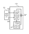
FIG. 2 shows a block schematic diagram of a receiver 200 according to a further embodiment of the present invention. The receiver 200 is coupled to a transmitter 203. A functionality of the receiver 200 is similar to the functionality of the receiver 100 from FIG. 1, wherein the receiver 200 comprises the optional features described in the following. It is understood that further embodiments of the present invention may include one, some or all of the additional features described in the following in conjunction with the receiver 200.
The receiver 200 comprises a controller 205 and a driver stage 207 for providing a supply voltage Vtr to the transmitter 203 based on control signals 209 a, 209 b. The controller 205 is configured to provide the control signals 209 a, 209 b to compensate changes of the supply voltage Vtr caused by a modulation of the current consumption (of a supply current Isensor) of the transmitter 203 such that the supply voltage Vtr of the transmitter 203 remains in a predefined range. Furthermore, the controller 205 is configured to evaluate a series of succeeding values of the control signals 209 a, 209 b to derive a message generated by the transmitter 203 by modulating its current consumption.
The controller 205 comprises a feedback analog-to-digital converter (feedback-ADC) 211 for obtaining a digital representation 213 of the supply voltage Vtr provided by the driver stage 207. As mentioned above, the feedback-ADC 211 maybe a 1-bit ADC (a comparator).
The controller 205 (or a digital control unit 215 of the controller 205) is configured to evaluate the digital representation 213 of the supply voltage Vtr to adjust the control signals 209 a, 209 b. By evaluating the digital representation 213 of the supply voltage Vtr the controller 205 can adjust the control signals 209 a, 209 b for controlling the driver stage 207 based on the digital representation 213 of the supply voltage Vtr only, in one embodiment.
Furthermore, by monitoring (for example storing) a series of succeeding values of the control signals 209 a, 209 b the controller 205 can obtain information describing the current consumption of the transmitter 203 and therefore a message sent by the transmitter 203 to the receiver 200. The controller 205 may continuously monitor the supply voltage Vtr of the transmitter 203 using the feedback-ADC 211 and may continuously adjust the control signals 209 a, 209 b and may furthermore evaluate the control signals 209 a, 209 b provided to the driver stage 207 for deriving messages sent by the transmitter 203. From FIG. 2 it can be seen that for driving the messages from the transmitter 203 one analog-to-digital converter is fully sufficient and an analog-to-digital converter for deriving the current consumption of the transmitter 203 is not necessary. Therefore, compared to conventional systems, in which the current consumption of the transmitter 203 is measured together with the supply voltage of the transmitter 203 one ADC or an analog control loop can be omitted, as the controller 205 derives the message generated by the transmitter 203 not based on a measurement of the current consumption of the transmitter 203 but based on the control signals 209 a, 209 b for compensating changes of the supply voltage Vtr caused by the current modulation of the transmitter 203.
As an example, the controller 205 may be configured such that different values of the control signals 209 a, 209 b correspond to different values of the supply current Isensor of the transmitter 203 and the controller 205 (or the digital control unit 215) may be configured to map the series of succeeding values of the control signals 209 a, 209 b to its corresponding values of the supply current Isensor of the transmitter 203 to derive a series of succeeding values of the supply current Isensor of the transmitter 203 representing the message generated by the transmitter 203. In an example, different values of the supply current Isensor may correspond with different information units (for example bits) of the message generated by the transmitter 203. In other words, the controller 205 may know (for example by using a digital model, a lookup table or by calibration) which values of the control signals 209 a, 209 b correspond to which values of the supply current Isensor of the transmitter 203 and therefore may derive the message generated by the transmitter 203 based on this information.
As an example for mapping values of the control signals 209 a, 209 b to values of the supply current Isensor of the transmitter 203, the controller 205 may comprise a digital model 217 of the driver stage 207 (or of an analog part of the driver stage 207). The digital model 217 may be configured to estimate (for example to calculate) the supply current of the supply current Isensor of the transmitter 203 based on the control signals 209 a, 209 b. The estimated supply current Iestimate of the transmitter 203 can be used by the controller 205 (or the digital control unit 215) to derive the message generated by the transmitter 203. In one embodiment, the digital model 217 may comprise a calculation rule for calculating the estimated supply current Iestimate based on the control signals 209 a, 209 b. A more detailed description of examples of the digital model 217 will be given below using the FIGS. 4a and 4b . The model may include the transient response of the driver e.g. a lowpass characteristic as well a nonlinear equation, e.g., the square law dependence of the drain current of a MOS transistor on the applied gate source voltage. The accuracy of the model can be limited to a level that is sufficient to receive the signal. This can be an approximation of the nonlinearity e.g. by a coarse lookup table or the limitation of the matching of the transient behavior to signals that are in the frequency range of the message that has to be received.
According to further embodiments, instead of using the digital model 217, the controller 205 may comprise a lookup table, the lookup table comprising a plurality of table entry pairs, each table entry pair comprising a value of the control signals 209 a, 209 b and its corresponding value of the supply current Isensor of the transmitter 203. The controller 205 may be configured to map a value of the control signals 209 a, 209 b to its associated value of the supply current Isensor of the transmitter 203 in the lookup table for deriving the information unit of the message generated by the transmitter 203 corresponding to the current value of the control signals 209 a, 209 b. For example, the lookup table may be calibrated by a vendor of the receiver 200 and be stored inside the controller 205. The lookup table can also have two independent variables e.g. the control signal itself and the previous sample of the control signal in order to cover a dynamic behavior. On the other hand the model could be split into two independent sections, e.g., a nonlinear equation or lookup table followed by a filter to model the dynamic behavior of the driver.
According to further embodiments the controller 205 (or the digital control unit 215) is configured to provide the control signals 209 a, 209 b as digital control signals. The driver stage 207 is configured to evaluate the digital control signals to provide the supply voltage Vtr based on the digital control signals. Furthermore, the digital control signals can be provided directly to the digital model 217 for calculating the estimated supply current Iestimate of the transmitter 203. The driver stage 207 comprises a first driver digital-to-analog converter (driver-DAC) 219 a and a second driver-DAC 219 b. The driver- DACs 219 a, 219 b may also be designated as gate driver DACs. Furthermore, the driver stage 207 comprises a first voltage controlled current source 221 a and a second voltage controlled current source 221 b for providing the supply voltage Vtr to the transmitter 203. The driver DACs 219 a, 219 b are configured to provide control voltages Vc1, Vc2 to the voltage controlled current sources 221 a, 221 b based on the digital control signals 209 a, 209 b. In other words, the driver DACs 219 a, 219 b are configured to derive the control voltages Vc1, Vc2 for controlling the voltage controlled current source 221 a, 221 b based on the digital control signals 209 a, 209 b.
Although in the example shown in FIG. 2 the controller 205 provides the two control signals 209 a, 209 b, according to further embodiments the controller 205 may also provide only one control signal and the driver stage 207 may derive the control voltage Vc1 for the first voltage current source 221 a and the control voltage Vc2 for the second current control voltage source 221 b based on the one control signal.
Furthermore, according to further embodiments, the driver stage 207 may comprise only one driver DAC and only one voltage control current source for providing the supply voltage Vtr for the transmitter 203 and therefore the controller 205 may also provide only one control signal to the driver stage 207.
In one embodiment of the receiver 200 shown in FIG. 2 the first voltage controlled current source 221 a is implemented using a first transistor 223 a. The second voltage control current source 221 b is implemented using a second transistor 223 b. The first transistor 223 a is a PMOS transistor and the second transistor 223 b is an NMOS transistor. A drain terminal 225 a of the first transistor 223 a is coupled to a drain terminal 225 b of the second transistor 223 b. The supply voltage Vtr of the transmitter 203 is provided at the drain terminal 225 a of the first transistor 223 a. The driver stage 207 is configured to vary a gate potential at a gate terminal 227 of the first transistor 223 a for controlling the drain source current Ip of the first transistor 220 a and therefore the supply voltage Vtr of the transmitter 203. The driver DAC 219 a is connected to the gate terminal 227 a of the first transistor 223 a for applying the first control voltage Vc1 as the gate potential of the first transistor 223 a. Furthermore, the supply voltage Vtr is a function of a drain source current In of the second transistor 223 b. The second driver DAC 219 b is connected to a gate terminal 227 b of the second transistor 223 b for applying the second control voltage Vc2 as the gate potential of the second transistor 223 b. Therefore, the supply voltage Vtr is a function of the drain source current Ip of the first transistor 223 a and of the drain source current In of the second transistor 223 b. The driver stage 207 controls the drain source currents Ip, In by varying the gate potentials of the transistors 223 a, 223 b based on the control signals 209 a, 209 b.
Furthermore, the feedback ADC 211 is coupled (for example directly connected) to the drain terminal 225 a of the first transistor 223 a for sensing the supply voltage Vtr.
As an example, upon a detection of an increased current consumption of the transmitter 203, the driver stage 207 may lower the gate potential (and therefore the first control voltage Vc1) of the first transistor 223 a, such that the drain source current Ip (or an absolute average value of the drain source current Ip) is increased, and may also lower the gate potential (and therefore the second control voltage Vc2) of the second transistor 223 b such that the drain source current In (or an absolute average value of the drain source current In) of the second transistor 223 b is decreased. Upon a detection of a decrease of the current consumption of the transmitter 203, the driver stage 207 may raise the gate potentials of the transistors 223 a, 223 b such that the drain source current Ip (or an absolute average value of the drain source current Ip) of the first transistor 223 a decreases and the drain source current In (or an absolute average value of the drain source current In) of the second transistor 223 b increases.
As mentioned before, according to further embodiments the second voltage controlled current source 221 b may be omitted, and therefore the second transistor 223 b may be omitted, such that the supply voltage Vtr is (only) a function of the drain source current Ip of the first transistor 223 a.
In short, the receiver 200 uses the PMOS and NMOS transistors 223 a, 223 b acting as controlled current sources 221 a, 221 b to increase or decrease the sensor supply current Isensor on demand of the (digital) controller 205 (or in demand of the digital control unit 215). Thus, the digital controls signals 209 a, 209 b influence the sensor supply current Isensor and the (digital) model 217 of the analog part can be expected to be simple.
According to some embodiments, the gate driver DACs 219 a, 219 b may be identical and the transistors 223 a, 223 b may have corresponding dimensions, such that a change of the current consumption of the transmitter 203 results in a change of the control voltages Vc1, Vc2 by the same voltage difference.
According to further embodiments the MOS transistors 223 a, 223 b may be replaced by transistors of other types, for example, by bipolar transistors. Therefore, a source terminal may correspond to an emitter terminal, a drain terminal may correspond to a collector terminal, a gate terminal may correspond to a base terminal and a drain source current may correspond to a collector emitter current.
As an example, the transmitter 203 may comprise a load (e.g. one or more wires and sensors).
FIG. 3a shows in a schematic circuit diagram a more detailed example of a possible implementation of the (analog part of the) driver stage 207 (of the supply regulator loop). The gate drivers (the analog parts of the driver DAC 219 a, 219 b) are implemented as current sources 331 a, 331 b, 333 a, 333 b that charge or discharge the gates 227 a, 227 b of the pass device MOS transistors 223 a, 223 b. The current sources 331 a, 331 b, 333 a, 333 b may be implemented, for example as switchable MOS current mirrors. The driver DACs 219 a, 219 b may be current steering DACs.
Based on the first control signal 209 a a first gate driver current source 331 a associated with the first transistor 223 a may charge the gate terminal 227 a of the first transistor 223 a and a second gate driver current source 333 a associated with the first transistor 223 a may discharge the gate terminal 227 a of the first transistor 223 a.
Based on the second control signal 209 b a first gate driver current source 331 b associated with the second transistor 223 b may charge the gate terminal 227 b of the second transistor 223 b and a second gate driver current source 333 b associated to the second transistor 223 b may discharge the gate terminal 227 b of the second transistor 223 b.
As already described, the current measurement of the supply current Isensor is derived from the digital control output signals 209 a, 209 b and estimated by the digital model 217 that describes the behavior of the regulators (the receiver's) analog part (e.g. the gate drivers 219 a, 219 b and the MOS pass devices 223 a, 223 b).
FIG. 4a shows in a schematic block diagram a possible implementation 217 a of the digital model 217 of the output stage (of the driver stage 207). A more simplified implementation 217 b of the digital model 217 is shown in FIG. 4 b.
The digital model 217 a shown in FIG. 4a simply consists of a digital representation of the gate driver mechanism comprising digital integrators or low pass filters 401 a, 401 b with a corner frequency below the frequency of a current modulation expected from the transmitter 203 (or from the sensor 203) and conversion constants 403 a, 403 b, 405 a, 405 b that represent the current DACs 219 a, 219 b and the transconductance of the pass device MOS transistors 223 a, 223 b.
The digital model 217 a receives as input signals the first digital control signal 209 a and the second control signal 209 b from the digital control unit 215 (may be also designated as digital controller 215). The conversion constants 403 a, 403 b (ILSBn, ILSBp) represent the gate driver DACs 219 a, 219 b converting the digital control signals 209 a, 209 b into the control voltages Vc1, Vc2 (or into charge currents for the gates of the transistors 223 a, 223 b). The integrators or low pass filters 401 a, 401 b model a low pass filter formed between inner resistances of the gate driver DACs 219 a, 219 b and the gate capacitances of the transistors 223 a, 223 b. The conversion constants 405 a, 405 b (gm _ NMOS, gm _ PMOS, gm _ NMOS) model the transistors 233 a, 233 b.
In the digital model 417 a shown in FIG. 4a nonlinearities of the transistors 223 a, 223 b are not regarded, as these do not significantly influence the decoding of the current modulated message of the transmitter 203.
Especially in cases in which the transmitter 203 uses slope based communication protocols (like Manchester), absolute values of the current consumption of the transmitter 203 are not as relevant as differences between the current consumption of the transmitter 203, therefore even the conversion constants 405 a, 405 b for the transistors 223 a, 223 b may be omitted.
As mentioned before, FIG. 4b shows in one embodiment a simplified version 217 b of the digital model 217 a shown in FIG. 4a . In the digital model 217 b all conversion constants from the digital model 217 a are collected into one common conversion constant 407 (ILSBp*gm _ PMOS/(ILSBn*gm _ NMOS)), since the model must only be proportional to the real physical current.
According to further embodiments, for a more precise calculation of the estimated sensor supply current Iestimate a more detailed MOS model (e.g. I=beta*(Ugs−Ut)2) may be used instead of the linearized conversion constant gm. This can easily be extended to models as they are used in circuit simulators. The same can be done for the driver stage 207 (and its conversion constants ILSBn, ILSBp).
As mentioned before, according to further embodiments only one transistor (for example the first transistor 223 a) may be sufficient to provide the supply voltage Vtr. In other words, other embodiments can be constructed using only one pass device, for example the PMOS transistor 223 a if no pull down current is required. In this case, the digital model 217 a can be modified such that the conversion constants 403 b, the integrator or low pass filter 401 b and the conversion constant 405 b may be omitted.
FIG. 7 shows an equivalent circuit of a driver stage 707 according to an embodiment of the present invention. The driver stage 707 may be an alternate implementation of the driver stage 107. As an example, the driver stage 207 of the receiver 200 may be replaced with the driver stage 707. In this case, only one digital control signal may be provided by the digital control unit 215 (for example the digital control signal 209 a). Furthermore, the digital model 217 may be adapted according to the driver stage 707.
The driver stage 707 comprises a current mirror 702, a cascode 704 (for example a high voltage cascode 704) and a current steering digital to analog converter 706 (IDAC), the driver stage 707 is coupled to a transmitter 703.
The current mirror 702 comprises a first input terminal 708 a and a second input terminal 708 b. The input terminals 708 a, 708 b are coupled to a supply node, for example, having the voltage Vsupply.
A first transistor 721 of the current mirror 702 may be in its functionality equal to the transistor 221 a. The first transistor 721 of the current mirror 702 provides the supply voltage for the transmitter 703 at its drain terminal and the driver stage 707 is configured to vary a gate potential of the first transistor 721 based on the control signal 209, such that the supply voltage is a function of a drain source current Irec of the transistor 721.
Furthermore, the current mirror 702 comprises a first output terminal 710 a and a second output terminal 710 b. The output terminals 710 a, 710 b are coupled to input terminal 712 a, 712 b of the cascode 704.
A first output terminal 714 a of the cascode 704 is coupled to a first current steering terminal 716 a of the current steering DAC 706. A second output terminal 714 b of the cascode 704 is coupled to a second current steering terminal 716 b of the current steering DAC 706.
The current steering DAC 706 is configured to generate a first (differential) current I1 from the current mirror 702 to the cascode 704 by steering a current into its first current steering terminal 716 a. This current I1 is mirrored by the current mirror 702, generating a second output current of the current mirror 702 Irec. The current Irec is split up into a first component, a second (differential) current I2 (into the cascode 704), and into a second component, the supply current Isensor for the transmitter 703.
In other words, the current steering DAC 706 steers the currents I1, I2 by sinking the currents I1, I2 in its current steering terminals 716 a, 716 b.
While the current mirror 702 generates the current Irec based on its transmission ratio (mirror scale factor) in dependence of the current I1, the current steering DAC 706 adjusts the current I2 by providing a (negative) current into its second current steering terminal 716 b.
The current steering DAC 706 generates the currents at its current steering terminals 716 a, 716 b differential, this means if it increases the current at its first current steering terminal 716 a, it decreases the current at its second current steering terminal 716 b and vice versa.
The current I1 may also be designated as control current for controlling the current mirror 702. The current mirror 702 acts as a current controlled current source (for the transmitter 103) providing the current Irec, and therefore also the supply current Isensor for the transmitter 103.
The current steering DAC 706, for example, may be an array of current sources.
The current steering DAC 706 adjusts the currents at its current steering terminals 716 a, 716 b in dependence on the digital feedback received from the controller 205 or the digital control unit 215 (in dependence on the digital control signal 209 a).
In one embodiment, the cascode 704 comprises a first transistor 718 a and a second transistor 718 b. The first transistor 718 a is coupled in-between the output terminal 710 a of the current mirror 702 and the first current steering terminal 716 a of the current steering DAC 706. The second transistor 718 b is coupled between the second output terminal 710 b of the current mirror 702 and the second current steering terminal 716 b of the current steering DAC 706. Gate terminals of the transistors 718 a, 718 b are coupled together and may be coupled to a fixed reference voltage source 730 providing the gate potentials for the gate terminals of the transistors 718 a, 718 b.
The cascode 704 provides constant potentials at the current steering terminal 716 a, 716 b (which are independent from the currents I1, I2). Furthermore, the cascode 704 acts as a high voltage cascode, this means voltages at the input terminals 712 a, 712 b of the cascode 704 may be larger than the voltages the current steering terminals 716 a, 716 b of the current steering DAC 706 can withstand. This enables a high supply voltage for the transmitter 103, for example, above 3V and below 15V, and a low supply voltage for the current steering DAC 706 (or for transistors of the current steering DAC 706), for example, below 3 Volt. A lower supply voltage for the current steering DAC 706 enables the use of transistors that are only compliant to low supply voltages (e.g. 1.5V) but allow a faster switching, and therefore a faster adaption of the currents I1, I2 upon a change of the supply current Isensor of the transmitter 103, caused by a current modulation.
Furthermore, the driver stage 707 may comprise a diode 720 for protection coupled in-between the second output terminal of the current mirror 702 and the second input terminal 712 b of the cascode 704.
The functionality of the driver stage 707 is equal to the functionality of the driver stage 207. The driver stage 707 regulates the current Irec such that it follows Isen (the internal supply voltage of the transmitter 703). A blocking capacitor of the transmitter 703 may be chosen such that a capacitor current Icap is negligible. The current steering DAC 706 may adjust the currents I1, I2 such that the supply voltage of the transmitter 703 (always) stays in the predetermined range. In other words, the current steering DAC 706 is controlled via the digital feedback loop to reduce or even minimize variations of the supply voltage, even during a current modulation performed by the transmitter 703, such that the current Icap along the blocking capacitor of the transmitter 703 is reduced or even minimized.
Therefore the closed loop (of transmitter 703 and driver stage 707) may have a gain close to 1 at frequencies that contribute to the sensor signal. As an example 189 kHz maybe the lowest spectral component in a transmission at 189 kBit/s. A bandwidth of the controller 205 may be chosen 2 MHz, such that at least some of the harmonics are taken into account (189 kHz*10≈2 MHz).
The open loop (without the transmitter 703) should have a gain larger 1 (e.g. larger 10).
Furthermore, a bandwidth of the controller 205 is chosen such that it is sufficient to follow the current.
The above mentioned especially applies for the frequency range of the signal of the message generated by the transmitter 703 by modulating its current consumption, for example as Manchester signal.
Using the current mirror 702 has the following advantages:
A fast proportional response, a gate voltage change is warped with a sqrt function of the diode and the sqrt function of the output transistor is compensated.
Although in the example of FIG. 7, the current mirror 702 is shown with a transmission ratio or mirror scale factor of 1:200, other transmission rates or mirror scale factors are also possible. Furthermore a current mirror can be introduced to scale the current I2 as well.
Although the transistors shown in FIG. 7 are MOSFET transistors, according to further embodiments, these transistors may be replaced by transistors of other types, for example, by bipolar transistors.
FIG. 5 shows a block schematic diagram of a receiver transmitter system 501 according to an embodiment of the present invention. The receiver transmitter system 501 comprises a receiver 500 (for example, being an electrical control unit or being comprised in an electrical control unit, for example, of a car). Furthermore, the receiver transmitter system 501 comprises a first transmitter 503 a (for example, comprising a sensor or being part of a sensor). The transmitter 503 a is coupled (for example, directly connected) to the receiver 500. A functionality of the receiver 500 may be similar to the functionality of the receiver 100. The receiver 500 may comprise further functionalities, for example as described in conjunction with the receiver 200 according to FIG. 2. The receiver 500 comprises a driver stage 507 and a controller 505. The functionality of the controller 505 may be similar to the functionality of the controller 105, wherein the controller 505 may comprise further functionalities. The functionality of the driver stage 507 may be similar to the functionality of the driver stage 107, wherein the driver stage 507 may comprise additional features, for example like those described in conjunction with the receiver 200 shown in FIG. 2.
The transmitter 503 a is configured to generate a message for the receiver 500 by modulating its current consumption.
According to further embodiments, the transmitter receiver system 501 may comprise a plurality of transmitters or sensors 503 a to 503 n, wherein each transmitter 503 a to 503 n is configured to generate a message for the receiver 500 by modulating its current consumption. The driver stage 507 of the receiver 500 is configured to provide the supply voltage Vtr to each of the transmitters 503 a to 503 n. Each transmitter 503 a to 503 n is configured to generate a message by modulating its current consumption during a given time slot allotted to the respective transmitter 503 a to 503 n. In other words, typically only one transmitter of the plurality of transmitters 503 a to 503 n is active at a time and modulates its current consumption. As mentioned before, the transmitters 503 a to 503 n may comprise sensors or may themselves be part of sensors, wherein a message generated by such a transmitter 503 a to 503 n comprises sensor data obtained by a sensor of the transmitter.
Furthermore, the receiver 500 may comprise an optional EMC protection diode 508 between a terminal for the supply voltage Vtr and a ground terminal.
According to further embodiments the current from the second output terminal of the IDAC is scaled by additional current mirrors before it is connected to the output
FIG. 6 shows a flow diagram of a method 600 according to a further embodiment.
The method 600 for receiving messages from a transmitter comprises a step 601 of providing a supply voltage to the transmitter based on a control signal.
Furthermore, the method 600 comprises a step 602 of providing the control signal to compensate for changes of the supply voltage caused by a modulation of the current consumption of the transmitter, such that the supply voltage remains in a predetermined range.
Furthermore, the method 600 comprises a step 603 of evaluating a series of succeeding values of the control signal to derive a message generated by the transmitter by modulating its current consumption.
This method 600 may be performed by a receiver (for example, by the receivers 100, 200, 500) according to an embodiment of the present invention.
According to an embodiment the receiver 100 may be a microcontroller or part of a microcontroller.
Although some aspects have been described in the context of an apparatus, it is clear that these aspects also represent a description of the corresponding method, where a block or device corresponds to a method step or a feature of a method step. Analogously, aspects described in the context of a method step also represent a description of a corresponding block or item or feature of a corresponding apparatus. Some or all of the method steps may be executed by (or using) a hardware apparatus, like for example, a microprocessor, a programmable computer or an electronic circuit. In some embodiments, some one or more of the most important method steps may be executed by such an apparatus.
Depending on certain implementation requirements, embodiments of the invention can be implemented in hardware or in software. The implementation can be performed using a digital storage medium, for example a floppy disk, a DVD, a Blue-Ray, a CD, a ROM, a PROM, an EPROM, an EEPROM or a FLASH memory, having electronically readable control signals stored thereon, which cooperate (or are capable of cooperating) with a programmable computer system such that the respective method is performed. Therefore, the digital storage medium may be computer readable.
Some embodiments according to the invention comprise a data carrier having electronically readable control signals, which are capable of cooperating with a programmable computer system, such that one of the methods described herein is performed.
Generally, embodiments of the present invention can be implemented as a computer program product with a program code, the program code being operative for performing one of the methods when the computer program product runs on a computer. The program code may for example be stored on a machine readable carrier.
Other embodiments comprise the computer program for performing one of the methods described herein, stored on a machine readable carrier.
In other words, an embodiment of the inventive method is, therefore, a computer program having a program code for performing one of the methods described herein, when the computer program runs on a computer.
A further embodiment of the inventive methods is, therefore, a data carrier (or a digital storage medium, or a computer-readable medium) comprising, recorded thereon, the computer program for performing one of the methods described herein. The data carrier, the digital storage medium or the recorded medium are typically tangible and/or non-transitionary.
A further embodiment of the inventive method is, therefore, a data stream or a sequence of signals representing the computer program for performing one of the methods described herein. The data stream or the sequence of signals may for example be configured to be transferred via a data communication connection, for example via the Internet.
A further embodiment comprises a processing means, for example a computer, or a programmable logic device, configured to or adapted to perform one of the methods described herein.
A further embodiment comprises a computer having installed thereon the computer program for performing one of the methods described herein.
A further embodiment according to the invention comprises an apparatus or a system configured to transfer (for example, electronically or optically) a computer program for performing one of the methods described herein to a receiver. The receiver may, for example, be a computer, a mobile device, a memory device or the like. The apparatus or system may, for example, comprise a file server for transferring the computer program to the receiver.
In some embodiments, a programmable logic device (for example a field programmable gate array) may be used to perform some or all of the functionalities of the methods described herein. In some embodiments, a field programmable gate array may cooperate with a microprocessor in order to perform one of the methods described herein. Generally, the methods are preferably performed by any hardware apparatus.
The above described embodiments are merely illustrative of the principles of the present invention. It is understood that modifications and variations of the arrangements and the details described herein will be apparent to others skilled in the art. It is the intent, therefore, to be limited only by the scope of the impending patent claims and not by the specific details presented by way of description and explanation of the embodiments herein.