US9455411B2 - Organic electroluminescent materials and devices - Google Patents
Organic electroluminescent materials and devices Download PDFInfo
- Publication number
- US9455411B2 US9455411B2 US14/611,468 US201514611468A US9455411B2 US 9455411 B2 US9455411 B2 US 9455411B2 US 201514611468 A US201514611468 A US 201514611468A US 9455411 B2 US9455411 B2 US 9455411B2
- Authority
- US
- United States
- Prior art keywords
- layer
- organic
- light emitting
- emitting device
- group
- Prior art date
- Legal status (The legal status is an assumption and is not a legal conclusion. Google has not performed a legal analysis and makes no representation as to the accuracy of the status listed.)
- Active
Links
- 239000000463 material Substances 0.000 title claims description 94
- 150000003957 organoselenium compounds Chemical class 0.000 claims abstract description 13
- 239000010410 layer Substances 0.000 claims description 97
- 239000002019 doping agent Substances 0.000 claims description 40
- -1 alkynel Chemical group 0.000 claims description 36
- 239000012044 organic layer Substances 0.000 claims description 22
- 125000003118 aryl group Chemical group 0.000 claims description 17
- 125000001424 substituent group Chemical group 0.000 claims description 13
- 230000000903 blocking effect Effects 0.000 claims description 12
- 125000000623 heterocyclic group Chemical group 0.000 claims description 11
- 125000001072 heteroaryl group Chemical group 0.000 claims description 9
- 125000000217 alkyl group Chemical group 0.000 claims description 8
- 125000003342 alkenyl group Chemical group 0.000 claims description 7
- 125000000753 cycloalkyl group Chemical group 0.000 claims description 7
- 125000001475 halogen functional group Chemical group 0.000 claims description 7
- 125000004404 heteroalkyl group Chemical group 0.000 claims description 5
- 125000003710 aryl alkyl group Chemical group 0.000 claims 2
- DHFABSXGNHDNCO-UHFFFAOYSA-N dibenzoselenophene Chemical compound C1=CC=C2C3=CC=CC=C3[se]C2=C1 DHFABSXGNHDNCO-UHFFFAOYSA-N 0.000 abstract description 8
- BNRDGHFESOHOBF-UHFFFAOYSA-N 1-benzoselenophene Chemical compound C1=CC=C2[se]C=CC2=C1 BNRDGHFESOHOBF-UHFFFAOYSA-N 0.000 abstract description 7
- FFGGMBALVXYUCQ-UHFFFAOYSA-N 2-benzoselenophene Chemical compound C1=CC=CC2=C[se]C=C21 FFGGMBALVXYUCQ-UHFFFAOYSA-N 0.000 abstract description 5
- YMWUJEATGCHHMB-UHFFFAOYSA-N Dichloromethane Chemical compound ClCCl YMWUJEATGCHHMB-UHFFFAOYSA-N 0.000 description 31
- 150000001875 compounds Chemical class 0.000 description 29
- 0 C1=CC2=C(C=C1)C1=C(/C=C\C=C/1)[Se]2.C1=CC2=C(C=C1)C1=C(/C=C\C=C/1)[Se]2.C1=CC2=C(C=C1)C1=C(C=C2)C2=C(/C=C3/C=CC=C/C3=C/2)[Se]1.C1=CC2=C(C=C1)C1=C(C=C2)C2=C(/C=C\C3=C2C=CC=C3)[Se]1.C1=CC2=C(C=C1)C1=C(C=C2)C2=C(/C=C\C=C/2)[Se]1.C1=CC2=C(C=C1)C1=C(C=C2)C2=C([Se]1)C1=C(C=CC=C1)/C=C\2.C1=CC2=C(C=C1)C1=C(C=C2)[Se]C2=C1/C=C1/C=CC=C/C1=C/2.C1=CC2=C(C=C1)C1=C(C=C2)[Se]C2=C1/C=C\C=C/2.C1=CC2=CC3=C(C=C2C=C1)C1=C(/C=C2/C=CC=C/C2=C/1)[Se]3.C1=CC2=CC3=C(C=C2C=C1)C1=C(/C=C\C=C/1)[Se]3.[1*]C.[1*]C.[1*]C.[1*]C.[1*]C.[1*]C.[1*]C.[1*]C.[1*]C.[1*]C.[2*]C.[2*]C.[2*]C.[2*]C.[2*]C.[2*]C.[2*]C.[2*]C.[2*]C Chemical compound C1=CC2=C(C=C1)C1=C(/C=C\C=C/1)[Se]2.C1=CC2=C(C=C1)C1=C(/C=C\C=C/1)[Se]2.C1=CC2=C(C=C1)C1=C(C=C2)C2=C(/C=C3/C=CC=C/C3=C/2)[Se]1.C1=CC2=C(C=C1)C1=C(C=C2)C2=C(/C=C\C3=C2C=CC=C3)[Se]1.C1=CC2=C(C=C1)C1=C(C=C2)C2=C(/C=C\C=C/2)[Se]1.C1=CC2=C(C=C1)C1=C(C=C2)C2=C([Se]1)C1=C(C=CC=C1)/C=C\2.C1=CC2=C(C=C1)C1=C(C=C2)[Se]C2=C1/C=C1/C=CC=C/C1=C/2.C1=CC2=C(C=C1)C1=C(C=C2)[Se]C2=C1/C=C\C=C/2.C1=CC2=CC3=C(C=C2C=C1)C1=C(/C=C2/C=CC=C/C2=C/1)[Se]3.C1=CC2=CC3=C(C=C2C=C1)C1=C(/C=C\C=C/1)[Se]3.[1*]C.[1*]C.[1*]C.[1*]C.[1*]C.[1*]C.[1*]C.[1*]C.[1*]C.[1*]C.[2*]C.[2*]C.[2*]C.[2*]C.[2*]C.[2*]C.[2*]C.[2*]C.[2*]C 0.000 description 28
- VLKZOEOYAKHREP-UHFFFAOYSA-N n-Hexane Chemical compound CCCCCC VLKZOEOYAKHREP-UHFFFAOYSA-N 0.000 description 24
- TVIVIEFSHFOWTE-UHFFFAOYSA-K tri(quinolin-8-yloxy)alumane Chemical compound [Al+3].C1=CN=C2C([O-])=CC=CC2=C1.C1=CN=C2C([O-])=CC=CC2=C1.C1=CN=C2C([O-])=CC=CC2=C1 TVIVIEFSHFOWTE-UHFFFAOYSA-K 0.000 description 23
- IJGRMHOSHXDMSA-UHFFFAOYSA-N Atomic nitrogen Chemical compound N#N IJGRMHOSHXDMSA-UHFFFAOYSA-N 0.000 description 22
- SLGBZMMZGDRARJ-UHFFFAOYSA-N Triphenylene Natural products C1=CC=C2C3=CC=CC=C3C3=CC=CC=C3C2=C1 SLGBZMMZGDRARJ-UHFFFAOYSA-N 0.000 description 16
- 229910052751 metal Inorganic materials 0.000 description 15
- 239000002184 metal Substances 0.000 description 15
- 239000000243 solution Substances 0.000 description 13
- 238000000034 method Methods 0.000 description 12
- 150000003384 small molecules Chemical class 0.000 description 12
- 229910052757 nitrogen Inorganic materials 0.000 description 11
- 125000005580 triphenylene group Chemical group 0.000 description 11
- 239000000203 mixture Substances 0.000 description 10
- LQNUZADURLCDLV-UHFFFAOYSA-N nitrobenzene Chemical compound [O-][N+](=O)C1=CC=CC=C1 LQNUZADURLCDLV-UHFFFAOYSA-N 0.000 description 10
- XLYOFNOQVPJJNP-UHFFFAOYSA-N water Substances O XLYOFNOQVPJJNP-UHFFFAOYSA-N 0.000 description 10
- YXFVVABEGXRONW-UHFFFAOYSA-N Toluene Chemical compound CC1=CC=CC=C1 YXFVVABEGXRONW-UHFFFAOYSA-N 0.000 description 9
- CSNNHWWHGAXBCP-UHFFFAOYSA-L Magnesium sulfate Chemical compound [Mg+2].[O-][S+2]([O-])([O-])[O-] CSNNHWWHGAXBCP-UHFFFAOYSA-L 0.000 description 8
- 230000000052 comparative effect Effects 0.000 description 8
- 238000004770 highest occupied molecular orbital Methods 0.000 description 8
- 239000007924 injection Substances 0.000 description 8
- 238000002347 injection Methods 0.000 description 8
- 239000003446 ligand Substances 0.000 description 8
- 238000004768 lowest unoccupied molecular orbital Methods 0.000 description 8
- 239000011541 reaction mixture Substances 0.000 description 8
- VFUDMQLBKNMONU-UHFFFAOYSA-N 9-[4-(4-carbazol-9-ylphenyl)phenyl]carbazole Chemical compound C12=CC=CC=C2C2=CC=CC=C2N1C1=CC=C(C=2C=CC(=CC=2)N2C3=CC=CC=C3C3=CC=CC=C32)C=C1 VFUDMQLBKNMONU-UHFFFAOYSA-N 0.000 description 7
- 150000004695 complexes Chemical class 0.000 description 7
- 238000000151 deposition Methods 0.000 description 7
- RAXXELZNTBOGNW-UHFFFAOYSA-N imidazole Natural products C1=CNC=N1 RAXXELZNTBOGNW-UHFFFAOYSA-N 0.000 description 7
- 239000000758 substrate Substances 0.000 description 7
- XEKOWRVHYACXOJ-UHFFFAOYSA-N Ethyl acetate Chemical compound CCOC(C)=O XEKOWRVHYACXOJ-UHFFFAOYSA-N 0.000 description 6
- IBHBKWKFFTZAHE-UHFFFAOYSA-N n-[4-[4-(n-naphthalen-1-ylanilino)phenyl]phenyl]-n-phenylnaphthalen-1-amine Chemical compound C1=CC=CC=C1N(C=1C2=CC=CC=C2C=CC=1)C1=CC=C(C=2C=CC(=CC=2)N(C=2C=CC=CC=2)C=2C3=CC=CC=C3C=CC=2)C=C1 IBHBKWKFFTZAHE-UHFFFAOYSA-N 0.000 description 6
- 239000011368 organic material Substances 0.000 description 6
- 239000007787 solid Substances 0.000 description 6
- DHDHJYNTEFLIHY-UHFFFAOYSA-N 4,7-diphenyl-1,10-phenanthroline Chemical group C1=CC=CC=C1C1=CC=NC2=C1C=CC1=C(C=3C=CC=CC=3)C=CN=C21 DHDHJYNTEFLIHY-UHFFFAOYSA-N 0.000 description 5
- UHOVQNZJYSORNB-UHFFFAOYSA-N Benzene Chemical compound C1=CC=CC=C1 UHOVQNZJYSORNB-UHFFFAOYSA-N 0.000 description 5
- 125000000304 alkynyl group Chemical group 0.000 description 5
- 239000000412 dendrimer Substances 0.000 description 5
- 229920000736 dendritic polymer Polymers 0.000 description 5
- 230000005525 hole transport Effects 0.000 description 5
- 230000005693 optoelectronics Effects 0.000 description 5
- 230000032258 transport Effects 0.000 description 5
- 125000005259 triarylamine group Chemical group 0.000 description 5
- LWIHDJKSTIGBAC-UHFFFAOYSA-K tripotassium phosphate Chemical compound [K+].[K+].[K+].[O-]P([O-])([O-])=O LWIHDJKSTIGBAC-UHFFFAOYSA-K 0.000 description 5
- JUJWROOIHBZHMG-UHFFFAOYSA-N Pyridine Chemical compound C1=CC=NC=C1 JUJWROOIHBZHMG-UHFFFAOYSA-N 0.000 description 4
- IOJUPLGTWVMSFF-UHFFFAOYSA-N benzothiazole Chemical compound C1=CC=C2SC=NC2=C1 IOJUPLGTWVMSFF-UHFFFAOYSA-N 0.000 description 4
- 230000015572 biosynthetic process Effects 0.000 description 4
- ILAHWRKJUDSMFH-UHFFFAOYSA-N boron tribromide Chemical compound BrB(Br)Br ILAHWRKJUDSMFH-UHFFFAOYSA-N 0.000 description 4
- 238000006243 chemical reaction Methods 0.000 description 4
- 229910052943 magnesium sulfate Inorganic materials 0.000 description 4
- 229920000642 polymer Polymers 0.000 description 4
- 238000010992 reflux Methods 0.000 description 4
- 238000003786 synthesis reaction Methods 0.000 description 4
- WJKHJLXJJJATHN-UHFFFAOYSA-N triflic anhydride Chemical compound FC(F)(F)S(=O)(=O)OS(=O)(=O)C(F)(F)F WJKHJLXJJJATHN-UHFFFAOYSA-N 0.000 description 4
- 229910000404 tripotassium phosphate Inorganic materials 0.000 description 4
- FCEHBMOGCRZNNI-UHFFFAOYSA-N 1-benzothiophene Chemical compound C1=CC=C2SC=CC2=C1 FCEHBMOGCRZNNI-UHFFFAOYSA-N 0.000 description 3
- XIWWHUAOOZIREN-UHFFFAOYSA-N 1-bromotriphenylene Chemical class C1=CC=CC2=C3C(Br)=CC=CC3=C(C=CC=C3)C3=C21 XIWWHUAOOZIREN-UHFFFAOYSA-N 0.000 description 3
- HYZJCKYKOHLVJF-UHFFFAOYSA-N 1H-benzimidazole Chemical compound C1=CC=C2NC=NC2=C1 HYZJCKYKOHLVJF-UHFFFAOYSA-N 0.000 description 3
- UJOBWOGCFQCDNV-UHFFFAOYSA-N Carbazole Natural products C1=CC=C2C3=CC=CC=C3NC2=C1 UJOBWOGCFQCDNV-UHFFFAOYSA-N 0.000 description 3
- YTPLMLYBLZKORZ-UHFFFAOYSA-N Thiophene Chemical compound C=1C=CSC=1 YTPLMLYBLZKORZ-UHFFFAOYSA-N 0.000 description 3
- 230000008901 benefit Effects 0.000 description 3
- 238000010586 diagram Methods 0.000 description 3
- ARZYTWDUGKFWJW-UHFFFAOYSA-N dibenzoselenophen-4-ylboronic acid Chemical compound C12=CC=CC=C2[se]C2=C1C=CC=C2B(O)O ARZYTWDUGKFWJW-UHFFFAOYSA-N 0.000 description 3
- IYYZUPMFVPLQIF-UHFFFAOYSA-N dibenzothiophene sulfoxide Natural products C1=CC=C2C3=CC=CC=C3SC2=C1 IYYZUPMFVPLQIF-UHFFFAOYSA-N 0.000 description 3
- GVEPBJHOBDJJJI-UHFFFAOYSA-N fluoranthene Chemical compound C1=CC(C2=CC=CC=C22)=C3C2=CC=CC3=C1 GVEPBJHOBDJJJI-UHFFFAOYSA-N 0.000 description 3
- 229910052741 iridium Inorganic materials 0.000 description 3
- GKOZUEZYRPOHIO-UHFFFAOYSA-N iridium atom Chemical compound [Ir] GKOZUEZYRPOHIO-UHFFFAOYSA-N 0.000 description 3
- 230000007246 mechanism Effects 0.000 description 3
- NIHNNTQXNPWCJQ-UHFFFAOYSA-N o-biphenylenemethane Natural products C1=CC=C2CC3=CC=CC=C3C2=C1 NIHNNTQXNPWCJQ-UHFFFAOYSA-N 0.000 description 3
- WCPAKWJPBJAGKN-UHFFFAOYSA-N oxadiazole Chemical compound C1=CON=N1 WCPAKWJPBJAGKN-UHFFFAOYSA-N 0.000 description 3
- 238000002390 rotary evaporation Methods 0.000 description 3
- 238000010898 silica gel chromatography Methods 0.000 description 3
- 239000002904 solvent Substances 0.000 description 3
- VNFWTIYUKDMAOP-UHFFFAOYSA-N sphos Chemical group COC1=CC=CC(OC)=C1C1=CC=CC=C1P(C1CCCCC1)C1CCCCC1 VNFWTIYUKDMAOP-UHFFFAOYSA-N 0.000 description 3
- 238000002207 thermal evaporation Methods 0.000 description 3
- 150000003852 triazoles Chemical class 0.000 description 3
- 239000011701 zinc Substances 0.000 description 3
- CYPYTURSJDMMMP-WVCUSYJESA-N (1e,4e)-1,5-diphenylpenta-1,4-dien-3-one;palladium Chemical compound [Pd].[Pd].C=1C=CC=CC=1\C=C\C(=O)\C=C\C1=CC=CC=C1.C=1C=CC=CC=1\C=C\C(=O)\C=C\C1=CC=CC=C1.C=1C=CC=CC=1\C=C\C(=O)\C=C\C1=CC=CC=C1 CYPYTURSJDMMMP-WVCUSYJESA-N 0.000 description 2
- QUGJLZNUGVQTGP-UHFFFAOYSA-N (3-triphenylen-2-ylphenyl) trifluoromethanesulfonate Chemical compound FC(F)(F)S(=O)(=O)OC1=CC=CC(C=2C=C3C4=CC=CC=C4C4=CC=CC=C4C3=CC=2)=C1 QUGJLZNUGVQTGP-UHFFFAOYSA-N 0.000 description 2
- AMSMVCOBCOZLEE-UHFFFAOYSA-N 1,3,5-Norcaratriene Chemical compound C1=CC=C2CC2=C1 AMSMVCOBCOZLEE-UHFFFAOYSA-N 0.000 description 2
- KXIFXZJZTKQHDW-UHFFFAOYSA-N 2-(3-methoxyphenyl)triphenylene Chemical group COC1=CC=CC(C=2C=C3C4=CC=CC=C4C4=CC=CC=C4C3=CC=2)=C1 KXIFXZJZTKQHDW-UHFFFAOYSA-N 0.000 description 2
- CGBWLVNDAHMWGP-UHFFFAOYSA-N 3-triphenylen-2-ylphenol Chemical compound OC1=CC=CC(C=2C=C3C4=CC=CC=C4C4=CC=CC=C4C3=CC=2)=C1 CGBWLVNDAHMWGP-UHFFFAOYSA-N 0.000 description 2
- KDCGOANMDULRCW-UHFFFAOYSA-N 7H-purine Chemical compound N1=CNC2=NC=NC2=C1 KDCGOANMDULRCW-UHFFFAOYSA-N 0.000 description 2
- PAYRUJLWNCNPSJ-UHFFFAOYSA-N Aniline Chemical compound NC1=CC=CC=C1 PAYRUJLWNCNPSJ-UHFFFAOYSA-N 0.000 description 2
- WKBOTKDWSSQWDR-UHFFFAOYSA-N Bromine atom Chemical compound [Br] WKBOTKDWSSQWDR-UHFFFAOYSA-N 0.000 description 2
- NSXJEEMTGWMJPY-UHFFFAOYSA-N C1=CC(N2C3=C(C=CC=C3)C3=C2C=CC=C3)=CC(C2=CC=CC(N3C4=C(C=CC=C4)C4=C3C=CC=C4)=C2)=C1 Chemical compound C1=CC(N2C3=C(C=CC=C3)C3=C2C=CC=C3)=CC(C2=CC=CC(N3C4=C(C=CC=C4)C4=C3C=CC=C4)=C2)=C1 NSXJEEMTGWMJPY-UHFFFAOYSA-N 0.000 description 2
- MZYDBGLUVPLRKR-UHFFFAOYSA-N C1=CC(N2C3=C(C=CC=C3)C3=C2C=CC=C3)=CC(N2C3=C(C=CC=C3)C3=C2C=CC=C3)=C1 Chemical compound C1=CC(N2C3=C(C=CC=C3)C3=C2C=CC=C3)=CC(N2C3=C(C=CC=C3)C3=C2C=CC=C3)=C1 MZYDBGLUVPLRKR-UHFFFAOYSA-N 0.000 description 2
- SDEFDICGRVDKPH-UHFFFAOYSA-M C1=CC2=C3C(=C1)O[AlH]/N3=C/C=C\2 Chemical compound C1=CC2=C3C(=C1)O[AlH]/N3=C/C=C\2 SDEFDICGRVDKPH-UHFFFAOYSA-M 0.000 description 2
- WXAIEIRYBSKHDP-UHFFFAOYSA-N C1=CC=C(C2=CC=C(N(C3=CC=C(C4=CC=CC=C4)C=C3)C3=CC=C(C4=CC=C(N(C5=CC=C(C6=CC=CC=C6)C=C5)C5=CC=C(C6=CC=CC=C6)C=C5)C=C4)C=C3)C=C2)C=C1 Chemical compound C1=CC=C(C2=CC=C(N(C3=CC=C(C4=CC=CC=C4)C=C3)C3=CC=C(C4=CC=C(N(C5=CC=C(C6=CC=CC=C6)C=C5)C5=CC=C(C6=CC=CC=C6)C=C5)C=C4)C=C3)C=C2)C=C1 WXAIEIRYBSKHDP-UHFFFAOYSA-N 0.000 description 2
- GEQBRULPNIVQPP-UHFFFAOYSA-N C1=CC=C(N2C(C3=CC(/C4=N/C5=C(C=CC=C5)N4C4=CC=CC=C4)=CC(/C4=N/C5=C(C=CC=C5)N4C4=CC=CC=C4)=C3)=NC3=C2C=CC=C3)C=C1 Chemical compound C1=CC=C(N2C(C3=CC(/C4=N/C5=C(C=CC=C5)N4C4=CC=CC=C4)=CC(/C4=N/C5=C(C=CC=C5)N4C4=CC=CC=C4)=C3)=NC3=C2C=CC=C3)C=C1 GEQBRULPNIVQPP-UHFFFAOYSA-N 0.000 description 2
- RPHSQWOMKHJGSI-UHFFFAOYSA-N C1=CC=C(N2C3=C(C=C(C4=CC(C5=CC6=C(C=C5)N(C5=CC=CC=C5)C5=C6C=C(C6=C/C=C7\C8=C(C=CN=C8)O\C7=C\6)C=C5)=CC=C4)C=C3)C3=C2C=CC(C2=C\C4=C(\C=C/2)C2=C(C=CN=C2)O4)=C3)C=C1 Chemical compound C1=CC=C(N2C3=C(C=C(C4=CC(C5=CC6=C(C=C5)N(C5=CC=CC=C5)C5=C6C=C(C6=C/C=C7\C8=C(C=CN=C8)O\C7=C\6)C=C5)=CC=C4)C=C3)C3=C2C=CC(C2=C\C4=C(\C=C/2)C2=C(C=CN=C2)O4)=C3)C=C1 RPHSQWOMKHJGSI-UHFFFAOYSA-N 0.000 description 2
- ZPXSBJSLTDIQDY-UHFFFAOYSA-N C1=CC=C2C(=C1)C1=C(/C=C\C=C/1)C2(C1=CC=C(C2=CC=C(N3C4=C(C=CC=C4)C4=C3C=CC=C4)C=C2)C=C1)C1=CC=C(C2=CC=C(N3C4=C(C=CC=C4)C4=C3C=CC=C4)C=C2)C=C1 Chemical compound C1=CC=C2C(=C1)C1=C(/C=C\C=C/1)C2(C1=CC=C(C2=CC=C(N3C4=C(C=CC=C4)C4=C3C=CC=C4)C=C2)C=C1)C1=CC=C(C2=CC=C(N3C4=C(C=CC=C4)C4=C3C=CC=C4)C=C2)C=C1 ZPXSBJSLTDIQDY-UHFFFAOYSA-N 0.000 description 2
- XYYYIVRDTLXJEF-UHFFFAOYSA-L CC1=N2/C3=C(C=CC=C3O[Al]2OC2=CC=C(C3=CC=CC=C3)C=C2)/C=C\1 Chemical compound CC1=N2/C3=C(C=CC=C3O[Al]2OC2=CC=C(C3=CC=CC=C3)C=C2)/C=C\1 XYYYIVRDTLXJEF-UHFFFAOYSA-L 0.000 description 2
- STTGYIUESPWXOW-UHFFFAOYSA-N CC1=NC2=C(C=CC3=C2N=C(C)C=C3C2=CC=CC=C2)C(C2=CC=CC=C2)=C1 Chemical compound CC1=NC2=C(C=CC3=C2N=C(C)C=C3C2=CC=CC=C2)C(C2=CC=CC=C2)=C1 STTGYIUESPWXOW-UHFFFAOYSA-N 0.000 description 2
- YLQBMQCUIZJEEH-UHFFFAOYSA-N Furan Chemical compound C=1C=COC=1 YLQBMQCUIZJEEH-UHFFFAOYSA-N 0.000 description 2
- SIKJAQJRHWYJAI-UHFFFAOYSA-N Indole Chemical compound C1=CC=C2NC=CC2=C1 SIKJAQJRHWYJAI-UHFFFAOYSA-N 0.000 description 2
- UFWIBTONFRDIAS-UHFFFAOYSA-N Naphthalene Chemical compound C1=CC=CC2=CC=CC=C21 UFWIBTONFRDIAS-UHFFFAOYSA-N 0.000 description 2
- KYQCOXFCLRTKLS-UHFFFAOYSA-N Pyrazine Chemical compound C1=CN=CC=N1 KYQCOXFCLRTKLS-UHFFFAOYSA-N 0.000 description 2
- KAESVJOAVNADME-UHFFFAOYSA-N Pyrrole Chemical compound C=1C=CNC=1 KAESVJOAVNADME-UHFFFAOYSA-N 0.000 description 2
- SMWDFEZZVXVKRB-UHFFFAOYSA-N Quinoline Chemical compound N1=CC=CC2=CC=CC=C21 SMWDFEZZVXVKRB-UHFFFAOYSA-N 0.000 description 2
- DZBUGLKDJFMEHC-UHFFFAOYSA-N acridine Chemical compound C1=CC=CC2=CC3=CC=CC=C3N=C21 DZBUGLKDJFMEHC-UHFFFAOYSA-N 0.000 description 2
- MWPLVEDNUUSJAV-UHFFFAOYSA-N anthracene Chemical compound C1=CC=CC2=CC3=CC=CC=C3C=C21 MWPLVEDNUUSJAV-UHFFFAOYSA-N 0.000 description 2
- 150000001491 aromatic compounds Chemical class 0.000 description 2
- CUFNKYGDVFVPHO-UHFFFAOYSA-N azulene Chemical compound C1=CC=CC2=CC=CC2=C1 CUFNKYGDVFVPHO-UHFFFAOYSA-N 0.000 description 2
- UFVXQDWNSAGPHN-UHFFFAOYSA-K bis[(2-methylquinolin-8-yl)oxy]-(4-phenylphenoxy)alumane Chemical compound [Al+3].C1=CC=C([O-])C2=NC(C)=CC=C21.C1=CC=C([O-])C2=NC(C)=CC=C21.C1=CC([O-])=CC=C1C1=CC=CC=C1 UFVXQDWNSAGPHN-UHFFFAOYSA-K 0.000 description 2
- GDTBXPJZTBHREO-UHFFFAOYSA-N bromine Substances BrBr GDTBXPJZTBHREO-UHFFFAOYSA-N 0.000 description 2
- 229910052794 bromium Inorganic materials 0.000 description 2
- WDECIBYCCFPHNR-UHFFFAOYSA-N chrysene Chemical compound C1=CC=CC2=CC=C3C4=CC=CC=C4C=CC3=C21 WDECIBYCCFPHNR-UHFFFAOYSA-N 0.000 description 2
- 239000003086 colorant Substances 0.000 description 2
- 238000004440 column chromatography Methods 0.000 description 2
- VPUGDVKSAQVFFS-UHFFFAOYSA-N coronene Chemical compound C1=C(C2=C34)C=CC3=CC=C(C=C3)C4=C4C3=CC=C(C=C3)C4=C2C3=C1 VPUGDVKSAQVFFS-UHFFFAOYSA-N 0.000 description 2
- 230000008021 deposition Effects 0.000 description 2
- 230000000694 effects Effects 0.000 description 2
- 239000003480 eluent Substances 0.000 description 2
- RMBPEFMHABBEKP-UHFFFAOYSA-N fluorene Chemical compound C1=CC=C2C3=C[CH]C=CC3=CC2=C1 RMBPEFMHABBEKP-UHFFFAOYSA-N 0.000 description 2
- 229910052737 gold Inorganic materials 0.000 description 2
- 239000010931 gold Substances 0.000 description 2
- 238000005286 illumination Methods 0.000 description 2
- 150000002460 imidazoles Chemical class 0.000 description 2
- UEEXRMUCXBPYOV-UHFFFAOYSA-N iridium;2-phenylpyridine Chemical group [Ir].C1=CC=CC=C1C1=CC=CC=N1.C1=CC=CC=C1C1=CC=CC=N1.C1=CC=CC=C1C1=CC=CC=N1 UEEXRMUCXBPYOV-UHFFFAOYSA-N 0.000 description 2
- AWJUIBRHMBBTKR-UHFFFAOYSA-N isoquinoline Chemical compound C1=NC=CC2=CC=CC=C21 AWJUIBRHMBBTKR-UHFFFAOYSA-N 0.000 description 2
- 230000007775 late Effects 0.000 description 2
- 238000004519 manufacturing process Methods 0.000 description 2
- 239000011159 matrix material Substances 0.000 description 2
- 239000012074 organic phase Substances 0.000 description 2
- 125000002524 organometallic group Chemical group 0.000 description 2
- 238000000059 patterning Methods 0.000 description 2
- YNPNZTXNASCQKK-UHFFFAOYSA-N phenanthrene Chemical compound C1=CC=C2C3=CC=CC=C3C=CC2=C1 YNPNZTXNASCQKK-UHFFFAOYSA-N 0.000 description 2
- GBROPGWFBFCKAG-UHFFFAOYSA-N picene Chemical compound C1=CC2=C3C=CC=CC3=CC=C2C2=C1C1=CC=CC=C1C=C2 GBROPGWFBFCKAG-UHFFFAOYSA-N 0.000 description 2
- 230000008569 process Effects 0.000 description 2
- 239000011241 protective layer Substances 0.000 description 2
- BBEAQIROQSPTKN-UHFFFAOYSA-N pyrene Chemical compound C1=CC=C2C=CC3=CC=CC4=CC=C1C2=C43 BBEAQIROQSPTKN-UHFFFAOYSA-N 0.000 description 2
- UMJSCPRVCHMLSP-UHFFFAOYSA-N pyridine Natural products COC1=CC=CN=C1 UMJSCPRVCHMLSP-UHFFFAOYSA-N 0.000 description 2
- XSCHRSMBECNVNS-UHFFFAOYSA-N quinoxaline Chemical compound N1=CC=NC2=CC=CC=C21 XSCHRSMBECNVNS-UHFFFAOYSA-N 0.000 description 2
- 229910052702 rhenium Inorganic materials 0.000 description 2
- HYERJXDYFLQTGF-UHFFFAOYSA-N rhenium Chemical compound [Re][Re][Re][Re][Re][Re][Re][Re][Re][Re][Re][Re][Re][Re][Re][Re][Re][Re][Re][Re][Re][Re][Re][Re][Re][Re][Re][Re][Re][Re][Re][Re][Re][Re][Re][Re][Re][Re][Re][Re][Re][Re][Re][Re][Re][Re][Re][Re][Re][Re][Re][Re][Re][Re][Re][Re][Re][Re][Re][Re][Re][Re][Re][Re][Re][Re][Re][Re] HYERJXDYFLQTGF-UHFFFAOYSA-N 0.000 description 2
- 229920006395 saturated elastomer Polymers 0.000 description 2
- 229910052710 silicon Inorganic materials 0.000 description 2
- 239000010703 silicon Substances 0.000 description 2
- 238000010129 solution processing Methods 0.000 description 2
- 238000003756 stirring Methods 0.000 description 2
- 239000000725 suspension Substances 0.000 description 2
- 229940015849 thiophene Drugs 0.000 description 2
- 229930192474 thiophene Natural products 0.000 description 2
- ITMCEJHCFYSIIV-UHFFFAOYSA-M triflate Chemical compound [O-]S(=O)(=O)C(F)(F)F ITMCEJHCFYSIIV-UHFFFAOYSA-M 0.000 description 2
- 238000005292 vacuum distillation Methods 0.000 description 2
- 229910052725 zinc Inorganic materials 0.000 description 2
- KTZQTRPPVKQPFO-UHFFFAOYSA-N 1,2-benzoxazole Chemical compound C1=CC=C2C=NOC2=C1 KTZQTRPPVKQPFO-UHFFFAOYSA-N 0.000 description 1
- MVKBGASYSLEJCU-UHFFFAOYSA-N 1,2-dibromotriphenylene Chemical group C1=CC=C2C3=C(Br)C(Br)=CC=C3C3=CC=CC=C3C2=C1 MVKBGASYSLEJCU-UHFFFAOYSA-N 0.000 description 1
- 125000001140 1,4-phenylene group Chemical group [H]C1=C([H])C([*:2])=C([H])C([H])=C1[*:1] 0.000 description 1
- DSAFSORWJPSMQS-UHFFFAOYSA-N 10H-phenothiazine 5-oxide Chemical compound C1=CC=C2S(=O)C3=CC=CC=C3NC2=C1 DSAFSORWJPSMQS-UHFFFAOYSA-N 0.000 description 1
- BAXOFTOLAUCFNW-UHFFFAOYSA-N 1H-indazole Chemical compound C1=CC=C2C=NNC2=C1 BAXOFTOLAUCFNW-UHFFFAOYSA-N 0.000 description 1
- HIXDQWDOVZUNNA-UHFFFAOYSA-N 2-(3,4-dimethoxyphenyl)-5-hydroxy-7-methoxychromen-4-one Chemical compound C=1C(OC)=CC(O)=C(C(C=2)=O)C=1OC=2C1=CC=C(OC)C(OC)=C1 HIXDQWDOVZUNNA-UHFFFAOYSA-N 0.000 description 1
- UXGVMFHEKMGWMA-UHFFFAOYSA-N 2-benzofuran Chemical compound C1=CC=CC2=COC=C21 UXGVMFHEKMGWMA-UHFFFAOYSA-N 0.000 description 1
- LYTMVABTDYMBQK-UHFFFAOYSA-N 2-benzothiophene Chemical compound C1=CC=CC2=CSC=C21 LYTMVABTDYMBQK-UHFFFAOYSA-N 0.000 description 1
- GEDOYYDMCZUHNW-UHFFFAOYSA-N 2-bromotriphenylene Chemical group C1=CC=C2C3=CC(Br)=CC=C3C3=CC=CC=C3C2=C1 GEDOYYDMCZUHNW-UHFFFAOYSA-N 0.000 description 1
- VHMICKWLTGFITH-UHFFFAOYSA-N 2H-isoindole Chemical compound C1=CC=CC2=CNC=C21 VHMICKWLTGFITH-UHFFFAOYSA-N 0.000 description 1
- DIVZFUBWFAOMCW-UHFFFAOYSA-N 4-n-(3-methylphenyl)-1-n,1-n-bis[4-(n-(3-methylphenyl)anilino)phenyl]-4-n-phenylbenzene-1,4-diamine Chemical group CC1=CC=CC(N(C=2C=CC=CC=2)C=2C=CC(=CC=2)N(C=2C=CC(=CC=2)N(C=2C=CC=CC=2)C=2C=C(C)C=CC=2)C=2C=CC(=CC=2)N(C=2C=CC=CC=2)C=2C=C(C)C=CC=2)=C1 DIVZFUBWFAOMCW-UHFFFAOYSA-N 0.000 description 1
- BPMFPOGUJAAYHL-UHFFFAOYSA-N 9H-Pyrido[2,3-b]indole Chemical compound C1=CC=C2C3=CC=CC=C3NC2=N1 BPMFPOGUJAAYHL-UHFFFAOYSA-N 0.000 description 1
- RSWGJHLUYNHPMX-UHFFFAOYSA-N Abietic-Saeure Natural products C12CCC(C(C)C)=CC2=CCC2C1(C)CCCC2(C)C(O)=O RSWGJHLUYNHPMX-UHFFFAOYSA-N 0.000 description 1
- 229910015845 BBr3 Inorganic materials 0.000 description 1
- FMMWHPNWAFZXNH-UHFFFAOYSA-N Benz[a]pyrene Chemical compound C1=C2C3=CC=CC=C3C=C(C=C3)C2=C2C3=CC=CC2=C1 FMMWHPNWAFZXNH-UHFFFAOYSA-N 0.000 description 1
- REWGEIGEXMMHLO-UHFFFAOYSA-N BrC1=CC2=C(C=C1)C1=C(C=CC=C1)C1=C2C=CC=C1.C.C1=CC2=C(C=C1)C1=C(C=CC=C1)C1=C2C=CC=C1.C1=CC2=C(C=C1)C1=C(C=CC=C1)C1=C2C=CC=C1.C1=CC2=C(C=C1)C1=C(C=CC=C1)C1=C2C=CC=C1.CBr.CBr.O=[N+]([O-])C1=CC=CC=C1 Chemical compound BrC1=CC2=C(C=C1)C1=C(C=CC=C1)C1=C2C=CC=C1.C.C1=CC2=C(C=C1)C1=C(C=CC=C1)C1=C2C=CC=C1.C1=CC2=C(C=C1)C1=C(C=CC=C1)C1=C2C=CC=C1.C1=CC2=C(C=C1)C1=C(C=CC=C1)C1=C2C=CC=C1.CBr.CBr.O=[N+]([O-])C1=CC=CC=C1 REWGEIGEXMMHLO-UHFFFAOYSA-N 0.000 description 1
- IBSAZSDRUFIVFU-UHFFFAOYSA-N BrC1=CC2=C(C=C1)C1=C(C=CC=C1)C1=C2C=[C+]C=C1.CC1=CC(C2=CC3=C(C=C2)C2=C(C=CC=C2)C2=C3C=CC=C2)=CC=C1.COC1=CC=CC(B(O)O)=C1.COC1=CC=CC(C)=C1C1=C(P(C2CCCCC2)C2CCCCC2)C=CC=C1 Chemical compound BrC1=CC2=C(C=C1)C1=C(C=CC=C1)C1=C2C=[C+]C=C1.CC1=CC(C2=CC3=C(C=C2)C2=C(C=CC=C2)C2=C3C=CC=C2)=CC=C1.COC1=CC=CC(B(O)O)=C1.COC1=CC=CC(C)=C1C1=C(P(C2CCCCC2)C2CCCCC2)C=CC=C1 IBSAZSDRUFIVFU-UHFFFAOYSA-N 0.000 description 1
- AYOMISFIGMZTGF-UHFFFAOYSA-N BrC1=CC=C(N(C2=CC=C(N(C3=C4C=CC=CC4=C4C=CC=CC4=C3)C3=C4C=CC=CC4=C4C=CC=CC4=C3)C=C2)C2=C3C=CC=CC3=C3C=CC=CC3=C2)C=C1 Chemical compound BrC1=CC=C(N(C2=CC=C(N(C3=C4C=CC=CC4=C4C=CC=CC4=C3)C3=C4C=CC=CC4=C4C=CC=CC4=C3)C=C2)C2=C3C=CC=CC3=C3C=CC=CC3=C2)C=C1 AYOMISFIGMZTGF-UHFFFAOYSA-N 0.000 description 1
- CELCDIFUYFKFFV-UHFFFAOYSA-M C(#C[Au]12C3=CC=CC=C3C3=CC=CC(=N31)C1=C2C=CC=C1)C1=CC=C(N(C2=CC=CC=C2)C2=CC=CC=C2)C=C1.C1=CC=C(C2=CC=N3C4=C2/C=C\C2=C(C5=CC=CC=C5)C=CN(=C24)[Pt]3(C2=CC=CC=C2)C2=CC=CC=C2)C=C1.C1=CC=C(O[Pt]23C4=C(C=CC=C4C4=CC=CC=N42)C2=CC=CC=N23)C=C1.CC.CC1=CC(C(F)(F)F)=NN1[Re]1(C=O)(C=O)(C=O)C2=CC=CC=C2C2=C1C=CC=C2.CF.FF.FF Chemical compound C(#C[Au]12C3=CC=CC=C3C3=CC=CC(=N31)C1=C2C=CC=C1)C1=CC=C(N(C2=CC=CC=C2)C2=CC=CC=C2)C=C1.C1=CC=C(C2=CC=N3C4=C2/C=C\C2=C(C5=CC=CC=C5)C=CN(=C24)[Pt]3(C2=CC=CC=C2)C2=CC=CC=C2)C=C1.C1=CC=C(O[Pt]23C4=C(C=CC=C4C4=CC=CC=N42)C2=CC=CC=N23)C=C1.CC.CC1=CC(C(F)(F)F)=NN1[Re]1(C=O)(C=O)(C=O)C2=CC=CC=C2C2=C1C=CC=C2.CF.FF.FF CELCDIFUYFKFFV-UHFFFAOYSA-M 0.000 description 1
- FSZHBEYFUBAVJU-UHFFFAOYSA-N C(#C[Au]12C3=CC=CC=C3C3=CC=CC(=N31)C1=CC=CC=C12)C1=CC=C(N(C2=CC=CC=C2)C2=CC=CC=C2)C=C1 Chemical compound C(#C[Au]12C3=CC=CC=C3C3=CC=CC(=N31)C1=CC=CC=C12)C1=CC=C(N(C2=CC=CC=C2)C2=CC=CC=C2)C=C1 FSZHBEYFUBAVJU-UHFFFAOYSA-N 0.000 description 1
- NHDZESQHWMKRPE-UHFFFAOYSA-N C.C.CCC Chemical compound C.C.CCC NHDZESQHWMKRPE-UHFFFAOYSA-N 0.000 description 1
- CXJZCYJDRARSJO-UHFFFAOYSA-N C/C1=N2\CC3=C(C=CC=C3)\C2=C\N1C.CN1/C=C2/C3=C(C4=CC=CC=C4)C=CN3C/N2=C/1.CN1/C=C\C2=N/1CC1=C2C=CC=C1.CN1/C=N2/CC3=C(C=CC=C3)/C2=N/1.CN1C2=C(C=CC=C2)N2CC3=C(C=CC=C3)[Ir]3(C4=CC=CC=C4C4=CC=NN43)C12.FC1=CC2=C(C(F)=C1)C1=C/N3C=CC=C\C3=N\1C2 Chemical compound C/C1=N2\CC3=C(C=CC=C3)\C2=C\N1C.CN1/C=C2/C3=C(C4=CC=CC=C4)C=CN3C/N2=C/1.CN1/C=C\C2=N/1CC1=C2C=CC=C1.CN1/C=N2/CC3=C(C=CC=C3)/C2=N/1.CN1C2=C(C=CC=C2)N2CC3=C(C=CC=C3)[Ir]3(C4=CC=CC=C4C4=CC=NN43)C12.FC1=CC2=C(C(F)=C1)C1=C/N3C=CC=C\C3=N\1C2 CXJZCYJDRARSJO-UHFFFAOYSA-N 0.000 description 1
- UNAMSKPNCSHLSB-UHFFFAOYSA-N C1=CC(C2=C3[Se]C4=C(C=CC=C4)C3=CC=C2)=CC(C2=CC=CC3=C2[Se]C2=C3C=CC=C2)=C1.C1=CC(C2=CC=CC3=C2[Se]C2=C3C=CC=C2)=CC(C2=CC3=C(C=C2)C2=C(C=CC=C2)C2=C3C=CC=C2)=C1.C1=CC(C2=CC=CC3=C2[Se]C2=C3C=CC=C2)=CC(C2=CC=CC(C3=CC=CC4=C3[Se]C3=C4C=CC=C3)=C2)=C1.C1=CC2=C(C=C1)C1=C(C=C(C3=CC4=C(C=C3)[Se]C3=C4/C=C(C4=CC5=C(C=C4)C4=C(C=CC=C4)C4=C5C=CC=C4)\C=C/3)C=C1)C1=C2C=CC=C1.C1=CC2=C(C=C1)C1=C(C=CC(C3=CC4=C(C=C3)C3=C(C=CC=C3)C3=C4C=CC=C3)=C1)[Se]2.C1=CC2=C(C=C1)C1=C([Se]2)/C(C2=CC3=C(C=C2)C2=C(C=CC=C2)C2=C3C=CC=C2)=C\C=C/1.C1=CC2=C(C=C1)C1=C([Se]2)/C(C2=CC=CC3=C2[Se]C2=C3/C=C\C=C/2C2=C3[Se]C4=C(/C=C\C=C/4)C3=CC=C2)=C\C=C/1.C1=CC2=C(C=C1)C1=CC=CC(C3=CC(N4C5=C(C=CC=C5)C5=C4C=CC=C5)=CC(N4C5=C(C=CC=C5)C5=C4C=CC=C5)=C3)=C1[Se]2.C1=CC2=C(C=C1)N(C1=CC3=C(C=C1)[Se]C1=C3/C=C(N3C4=C(C=CC=C4)C4=C3C=CC=C4)\C=C/1)C1=C2C=CC=C1.C1=CC2=C([Se]C3=C2/C=C\C=C/3N2C3=C(C=CC=C3)C3=C2C=CC=C3)C(N2C3=C(C=CC=C3)C3=C2C=CC=C3)=C1.C1=CC=C(C2=C(C3=CC=CC4=C3[Se]C3=C4C=CC=C3)C=CC=C2)C(C2=CC=CC3=C2[Se]C2=C3C=CC=C2)=C1 Chemical compound C1=CC(C2=C3[Se]C4=C(C=CC=C4)C3=CC=C2)=CC(C2=CC=CC3=C2[Se]C2=C3C=CC=C2)=C1.C1=CC(C2=CC=CC3=C2[Se]C2=C3C=CC=C2)=CC(C2=CC3=C(C=C2)C2=C(C=CC=C2)C2=C3C=CC=C2)=C1.C1=CC(C2=CC=CC3=C2[Se]C2=C3C=CC=C2)=CC(C2=CC=CC(C3=CC=CC4=C3[Se]C3=C4C=CC=C3)=C2)=C1.C1=CC2=C(C=C1)C1=C(C=C(C3=CC4=C(C=C3)[Se]C3=C4/C=C(C4=CC5=C(C=C4)C4=C(C=CC=C4)C4=C5C=CC=C4)\C=C/3)C=C1)C1=C2C=CC=C1.C1=CC2=C(C=C1)C1=C(C=CC(C3=CC4=C(C=C3)C3=C(C=CC=C3)C3=C4C=CC=C3)=C1)[Se]2.C1=CC2=C(C=C1)C1=C([Se]2)/C(C2=CC3=C(C=C2)C2=C(C=CC=C2)C2=C3C=CC=C2)=C\C=C/1.C1=CC2=C(C=C1)C1=C([Se]2)/C(C2=CC=CC3=C2[Se]C2=C3/C=C\C=C/2C2=C3[Se]C4=C(/C=C\C=C/4)C3=CC=C2)=C\C=C/1.C1=CC2=C(C=C1)C1=CC=CC(C3=CC(N4C5=C(C=CC=C5)C5=C4C=CC=C5)=CC(N4C5=C(C=CC=C5)C5=C4C=CC=C5)=C3)=C1[Se]2.C1=CC2=C(C=C1)N(C1=CC3=C(C=C1)[Se]C1=C3/C=C(N3C4=C(C=CC=C4)C4=C3C=CC=C4)\C=C/1)C1=C2C=CC=C1.C1=CC2=C([Se]C3=C2/C=C\C=C/3N2C3=C(C=CC=C3)C3=C2C=CC=C3)C(N2C3=C(C=CC=C3)C3=C2C=CC=C3)=C1.C1=CC=C(C2=C(C3=CC=CC4=C3[Se]C3=C4C=CC=C3)C=CC=C2)C(C2=CC=CC3=C2[Se]C2=C3C=CC=C2)=C1 UNAMSKPNCSHLSB-UHFFFAOYSA-N 0.000 description 1
- MEWQVORVYGJYGD-UHFFFAOYSA-N C1=CC(C2=CC(C3=C4\[Se]C5=C(C=CC=C5)\C4=C/C=C\3)=CC=C2)=CC(C2=C3\[Se]C4=C(C=CC=C4)\C3=C/C=C\2)=C1.CC1=CC=CC(C2=CC(OS(=O)(=O)C(F)(F)F)=CC=C2)=C1.OB(O)/C1=C/C=C\C2=C1[Se]C1=CC=CC=C12.[H-2] Chemical compound C1=CC(C2=CC(C3=C4\[Se]C5=C(C=CC=C5)\C4=C/C=C\3)=CC=C2)=CC(C2=C3\[Se]C4=C(C=CC=C4)\C3=C/C=C\2)=C1.CC1=CC=CC(C2=CC(OS(=O)(=O)C(F)(F)F)=CC=C2)=C1.OB(O)/C1=C/C=C\C2=C1[Se]C1=CC=CC=C12.[H-2] MEWQVORVYGJYGD-UHFFFAOYSA-N 0.000 description 1
- LIIAMJDDLPKQDF-UHFFFAOYSA-N C1=CC(C2=CC3=C(C=C2)C2=C(C=CC=C2)C2=C3C=CC=C2)=CC(/C2=C3\C=CC=C\C3=C(/C3=CC(C4=CC5=C(C=C4)C4=C(C=CC=C4)C4=C5C=CC=C4)=CC=C3)[Se]2)=C1.C1=CC(C2=CC3=C(C=C2)C2=C(C=CC=C2)C2=C3C=CC=C2)=CC(C2=C3[Se]C=CC3=CC=C2)=C1.C1=CC2=C(C=C1)C1=C(C=C(C3=C4C=CC=CC4=C(C4=C/C5=C(/C=C/4)C4=C(C=CC=C4)C4=C5C=CC=C4)[Se]3)C=C1)C1=C2C=CC=C1.C1=CC2=C(C=C1)C1=C(C=C(C3=C4[Se]C=CC4=CC=C3)C=C1)C1=C2C=CC=C1.C1=CC=C(C2=C(C3=CC=CC=C3)C3=CC=CC(C4=CC5=C(C=C4)C4=C(C=CC=C4)C4=C5C=CC=C4)=C3[Se]2)C=C1 Chemical compound C1=CC(C2=CC3=C(C=C2)C2=C(C=CC=C2)C2=C3C=CC=C2)=CC(/C2=C3\C=CC=C\C3=C(/C3=CC(C4=CC5=C(C=C4)C4=C(C=CC=C4)C4=C5C=CC=C4)=CC=C3)[Se]2)=C1.C1=CC(C2=CC3=C(C=C2)C2=C(C=CC=C2)C2=C3C=CC=C2)=CC(C2=C3[Se]C=CC3=CC=C2)=C1.C1=CC2=C(C=C1)C1=C(C=C(C3=C4C=CC=CC4=C(C4=C/C5=C(/C=C/4)C4=C(C=CC=C4)C4=C5C=CC=C4)[Se]3)C=C1)C1=C2C=CC=C1.C1=CC2=C(C=C1)C1=C(C=C(C3=C4[Se]C=CC4=CC=C3)C=C1)C1=C2C=CC=C1.C1=CC=C(C2=C(C3=CC=CC=C3)C3=CC=CC(C4=CC5=C(C=C4)C4=C(C=CC=C4)C4=C5C=CC=C4)=C3[Se]2)C=C1 LIIAMJDDLPKQDF-UHFFFAOYSA-N 0.000 description 1
- WATAMNJGMCGDDT-UHFFFAOYSA-N C1=CC(C2=CC3=C(C=C2)C2=C(C=CC=C2)C2=C3C=CC=C2)=CC(C2=C3\[Se]C4=C(C=CC=C4)\C3=C/C=C\2)=C1.O=S(=O)(OC1=CC=CC(C2=CC3=C(C=C2)C2=C(C=CC=C2)C2=C3C=CC=C2)=C1)C(F)(F)F.OB(O)/C1=C/C=C\C2=C1[Se]C1=CC=CC=C12.[H-] Chemical compound C1=CC(C2=CC3=C(C=C2)C2=C(C=CC=C2)C2=C3C=CC=C2)=CC(C2=C3\[Se]C4=C(C=CC=C4)\C3=C/C=C\2)=C1.O=S(=O)(OC1=CC=CC(C2=CC3=C(C=C2)C2=C(C=CC=C2)C2=C3C=CC=C2)=C1)C(F)(F)F.OB(O)/C1=C/C=C\C2=C1[Se]C1=CC=CC=C12.[H-] WATAMNJGMCGDDT-UHFFFAOYSA-N 0.000 description 1
- FEEVDOPOKYHDKB-UHFFFAOYSA-N C1=CC(C2=CC3=C(C=C2)C2=C(C=CC=C2)C2=C3C=CC=C2)=CC(C2=CC3=C(C=C2)C2=C(C=CC=C2)C2=C3C=CC=C2)=C1 Chemical compound C1=CC(C2=CC3=C(C=C2)C2=C(C=CC=C2)C2=C3C=CC=C2)=CC(C2=CC3=C(C=C2)C2=C(C=CC=C2)C2=C3C=CC=C2)=C1 FEEVDOPOKYHDKB-UHFFFAOYSA-N 0.000 description 1
- RPCGZCVCMSVTAN-UHFFFAOYSA-N C1=CC(C2=CC3=C(C=C2)C2=C(C=CC=C2)C2=C3C=CC=C2)=CC(C2=CC3=C(C=CC=C3)[Se]2)=C1.C1=CC2=C(C=C1)[Se]/C(C1=CC3=C(C=C1)C1=C(C=CC=C1)C1=C3C=CC=C1)=C\2.C1=CC=C(C2=C(C3=CC=CC=C3)C3=CC(C4=CC=CC(C5=CC6=C(C=C5)C5=C(C=CC=C5)C5=C6C=CC=C5)=C4)=CC=C3[Se]2)C=C1 Chemical compound C1=CC(C2=CC3=C(C=C2)C2=C(C=CC=C2)C2=C3C=CC=C2)=CC(C2=CC3=C(C=CC=C3)[Se]2)=C1.C1=CC2=C(C=C1)[Se]/C(C1=CC3=C(C=C1)C1=C(C=CC=C1)C1=C3C=CC=C1)=C\2.C1=CC=C(C2=C(C3=CC=CC=C3)C3=CC(C4=CC=CC(C5=CC6=C(C=C5)C5=C(C=CC=C5)C5=C6C=CC=C5)=C4)=CC=C3[Se]2)C=C1 RPCGZCVCMSVTAN-UHFFFAOYSA-N 0.000 description 1
- IMKXSEPQICZHSL-UHFFFAOYSA-N C1=CC(C2=CC3=C(C=C2)SC2=C3C=CC=C2)=CC(C2=CC(N3C4=C(C=CC=C4)C4=C3C=CC=C4)=CC=C2)=C1 Chemical compound C1=CC(C2=CC3=C(C=C2)SC2=C3C=CC=C2)=CC(C2=CC(N3C4=C(C=CC=C4)C4=C3C=CC=C4)=CC=C2)=C1 IMKXSEPQICZHSL-UHFFFAOYSA-N 0.000 description 1
- QKVWPNRUXZYLQV-UHFFFAOYSA-N C1=CC(C2=CC=C3C(=C2)C2=C(C=CC=C2)C2=C3C=CC=C2)=CC(C2=CC=CC3=C2SC2=C3C=CC=C2)=C1 Chemical compound C1=CC(C2=CC=C3C(=C2)C2=C(C=CC=C2)C2=C3C=CC=C2)=CC(C2=CC=CC3=C2SC2=C3C=CC=C2)=C1 QKVWPNRUXZYLQV-UHFFFAOYSA-N 0.000 description 1
- DGBNJNQFQFPIIR-UHFFFAOYSA-N C1=CC(C2=CC=C3[Se]C4=C(C=CC=C4)C3=C2)=CC(C2=CC=CC(C3=CC4=C(C=C3)[Se]C3=C4C=CC=C3)=C2)=C1.C1=CC2=C(C=C1)C1(C3=C2C=C(C2=C/C4=C(\C=C/2)[Se]C2=C4C=C(C4=C/C5=C(\C=C/4)C4(C6=C(C=CC=C6)C6=C4C=CC=C6)C4=C5C=CC=C4)C=C2)C=C3)C2=C(C=CC=C2)C2=C1/C=C\C=C/2.C1=CC2=C(C=C1)C1(C3=C2C=CC=C3)C2=C(C=CC=C2)C2=C1/C=C(C1=C/C3=C(\C=C/1)[Se]C1=C3C=C(C3=C/C=C4\C5=C(C=CC=C5)C5(C6=C(C=CC=C6)C6=C5C=CC=C6)\C4=C\3)C=C1)\C=C/2.C1=CC2=C(C=C1)C1=C([Se]2)/C(C2=CC3=C(C=C2)[Se]C2=C3/C=C(C3=C4\[Se]C5=C(C=CC=C5)\C4=C\C=C/3)\C=C/2)=C\C=C/1.C1=CC2=C(C=C1)C1=CC=CC(N(C3=C4[Se]C5=C(C=CC=C5)C4=CC=C3)C3=C4[Se]C5=C(C=CC=C5)C4=CC=C3)=C1[Se]2.C1=CC2=C(C=C1)C1=C\C(N3C4=C(C=CC=C4)C4=C3C=CC(N3C5=C(C=CC=C5)C5=C3C=CC=C5)=C4)=C/C=C\1[Se]2.O=C(C1=CC2=C(C=C1)[Se]C1=C2/C=C(C(=O)/C2=C/C=C\C3=C2[Se]C2=C3C=CC=C2)\C=C/1)/C1=C/C=C\C2=C1[Se]C1=C2C=CC=C1 Chemical compound C1=CC(C2=CC=C3[Se]C4=C(C=CC=C4)C3=C2)=CC(C2=CC=CC(C3=CC4=C(C=C3)[Se]C3=C4C=CC=C3)=C2)=C1.C1=CC2=C(C=C1)C1(C3=C2C=C(C2=C/C4=C(\C=C/2)[Se]C2=C4C=C(C4=C/C5=C(\C=C/4)C4(C6=C(C=CC=C6)C6=C4C=CC=C6)C4=C5C=CC=C4)C=C2)C=C3)C2=C(C=CC=C2)C2=C1/C=C\C=C/2.C1=CC2=C(C=C1)C1(C3=C2C=CC=C3)C2=C(C=CC=C2)C2=C1/C=C(C1=C/C3=C(\C=C/1)[Se]C1=C3C=C(C3=C/C=C4\C5=C(C=CC=C5)C5(C6=C(C=CC=C6)C6=C5C=CC=C6)\C4=C\3)C=C1)\C=C/2.C1=CC2=C(C=C1)C1=C([Se]2)/C(C2=CC3=C(C=C2)[Se]C2=C3/C=C(C3=C4\[Se]C5=C(C=CC=C5)\C4=C\C=C/3)\C=C/2)=C\C=C/1.C1=CC2=C(C=C1)C1=CC=CC(N(C3=C4[Se]C5=C(C=CC=C5)C4=CC=C3)C3=C4[Se]C5=C(C=CC=C5)C4=CC=C3)=C1[Se]2.C1=CC2=C(C=C1)C1=C\C(N3C4=C(C=CC=C4)C4=C3C=CC(N3C5=C(C=CC=C5)C5=C3C=CC=C5)=C4)=C/C=C\1[Se]2.O=C(C1=CC2=C(C=C1)[Se]C1=C2/C=C(C(=O)/C2=C/C=C\C3=C2[Se]C2=C3C=CC=C2)\C=C/1)/C1=C/C=C\C2=C1[Se]C1=C2C=CC=C1 DGBNJNQFQFPIIR-UHFFFAOYSA-N 0.000 description 1
- JWRYXQCPEAAYBP-UHFFFAOYSA-N C1=CC(C2=CC=C3[Se]C4=C(C=CC=C4)C3=C2)=CC(C2=CC=CC(C3=CC4=C(C=C3)[Se]C3=C4C=CC=C3)=C2)=C1.C1=CC2=C(C=C1)C1(C3=CC(C4=CC5=C(C=C4)[Se]C4=C5/C=C(C5=CC6=C(C=C5)C5=C(C=CC=C5)C65C6=C(C=CC=C6)C6=C5C=CC=C6)\C=C/4)=CC=C32)C2=C(C=CC=C2)C2=C1C=CC=C2.C1=CC2=C(C=C1)C1=CC=CC(N(C3=C4[Se]C5=C(C=CC=C5)C4=CC=C3)C3=C4[Se]C5=C(C=CC=C5)C4=CC=C3)=C1[Se]2.C1=CC=C2C(=C1)C1=C(C=CC=C1)C21C2=C(C=CC=C2)C2=C1C=CC(C1=C/C3=C(\C=C/1)[Se]C1=C3C=C(C3=CC=C4C(=C3)C3=C(C=CC=C3)C43C4=C(C=CC=C4)C4=C3C=CC=C4)C=C1)=C2.O=C(C1=CC2=C(C=C1)[Se]C1=C2/C=C(C(=O)C2=CC=CC3=C2[Se]C2=C3C=CC=C2)\C=C/1)C1=C2[Se]C3=C(C=CC=C3)C2=CC=C1 Chemical compound C1=CC(C2=CC=C3[Se]C4=C(C=CC=C4)C3=C2)=CC(C2=CC=CC(C3=CC4=C(C=C3)[Se]C3=C4C=CC=C3)=C2)=C1.C1=CC2=C(C=C1)C1(C3=CC(C4=CC5=C(C=C4)[Se]C4=C5/C=C(C5=CC6=C(C=C5)C5=C(C=CC=C5)C65C6=C(C=CC=C6)C6=C5C=CC=C6)\C=C/4)=CC=C32)C2=C(C=CC=C2)C2=C1C=CC=C2.C1=CC2=C(C=C1)C1=CC=CC(N(C3=C4[Se]C5=C(C=CC=C5)C4=CC=C3)C3=C4[Se]C5=C(C=CC=C5)C4=CC=C3)=C1[Se]2.C1=CC=C2C(=C1)C1=C(C=CC=C1)C21C2=C(C=CC=C2)C2=C1C=CC(C1=C/C3=C(\C=C/1)[Se]C1=C3C=C(C3=CC=C4C(=C3)C3=C(C=CC=C3)C43C4=C(C=CC=C4)C4=C3C=CC=C4)C=C1)=C2.O=C(C1=CC2=C(C=C1)[Se]C1=C2/C=C(C(=O)C2=CC=CC3=C2[Se]C2=C3C=CC=C2)\C=C/1)C1=C2[Se]C3=C(C=CC=C3)C2=CC=C1 JWRYXQCPEAAYBP-UHFFFAOYSA-N 0.000 description 1
- KLAUKHTXECXQDG-UHFFFAOYSA-N C1=CC(C2=CC=C3[Se]C4=C(C=CC=C4)C3=C2)=CC(C2=CC=CC(C3=CC4=C(C=C3)[Se]C3=C4C=CC=C3)=C2)=C1.C1=CC2=C(C=C1)C1=C([Se]2)C(N(C2=CC=C(C3=CC=C(N(C4=CC=CC5=C4[Se]C4=C5C=CC=C4)C4=CC=CC5=C4[Se]C4=C5C=CC=C4)C=C3)C=C2)C2=CC=CC3=C2[Se]C2=C3C=CC=C2)=CC=C1.C1=CC2=C(C=C1)C1=CC=CC(N(C3=C4[Se]C5=C(C=CC=C5)C4=CC=C3)C3=C4[Se]C5=C(C=CC=C5)C4=CC=C3)=C1[Se]2.C1=CC=C(N(C2=CC=C(C3=CC=C(N(C4=CC=CC=C4)C4=CC=C5[Se]C6=CC=CCC6=C5C4)C=C3)C=C2)C2=CC=C3[Se]C4=CC=CCC4=C3C2)C=C1.C1=CC=C(N(C2=CC=C(C3=CC=C(N(C4=CC=CC=C4)C4=CC=CC5=C4[Se]C4=C5C=CC=C4)C=C3)C=C2)C2=CC=CC3=C2[Se]C2=C3C=CC=C2)C=C1.C1=CCC2=C3CC(N(C4=CC=C(C5=CC=C(N(C6=CC7=C(C=C6)[Se]C6=C7C=CC=C6)C6=CC=C7[Se]C8=CC=CCC8=C7C6)C=C5)C=C4)C4=CC5=C(C=C4)[Se]C4=C5C=CC=C4)=CC=C3[Se]C2=C1 Chemical compound C1=CC(C2=CC=C3[Se]C4=C(C=CC=C4)C3=C2)=CC(C2=CC=CC(C3=CC4=C(C=C3)[Se]C3=C4C=CC=C3)=C2)=C1.C1=CC2=C(C=C1)C1=C([Se]2)C(N(C2=CC=C(C3=CC=C(N(C4=CC=CC5=C4[Se]C4=C5C=CC=C4)C4=CC=CC5=C4[Se]C4=C5C=CC=C4)C=C3)C=C2)C2=CC=CC3=C2[Se]C2=C3C=CC=C2)=CC=C1.C1=CC2=C(C=C1)C1=CC=CC(N(C3=C4[Se]C5=C(C=CC=C5)C4=CC=C3)C3=C4[Se]C5=C(C=CC=C5)C4=CC=C3)=C1[Se]2.C1=CC=C(N(C2=CC=C(C3=CC=C(N(C4=CC=CC=C4)C4=CC=C5[Se]C6=CC=CCC6=C5C4)C=C3)C=C2)C2=CC=C3[Se]C4=CC=CCC4=C3C2)C=C1.C1=CC=C(N(C2=CC=C(C3=CC=C(N(C4=CC=CC=C4)C4=CC=CC5=C4[Se]C4=C5C=CC=C4)C=C3)C=C2)C2=CC=CC3=C2[Se]C2=C3C=CC=C2)C=C1.C1=CCC2=C3CC(N(C4=CC=C(C5=CC=C(N(C6=CC7=C(C=C6)[Se]C6=C7C=CC=C6)C6=CC=C7[Se]C8=CC=CCC8=C7C6)C=C5)C=C4)C4=CC5=C(C=C4)[Se]C4=C5C=CC=C4)=CC=C3[Se]C2=C1 KLAUKHTXECXQDG-UHFFFAOYSA-N 0.000 description 1
- KFKHNBPNJMWUEG-UHFFFAOYSA-N C1=CC(C2=CC=CC(C3=CC4=C(C=C3)C3=C(C=CC=C3)C3=C4C=CC=C3)=C2)=CC(C2=CC3=C(C=C2)C2=C(C=CC=C2)C2=C3C=CC=C2)=C1 Chemical compound C1=CC(C2=CC=CC(C3=CC4=C(C=C3)C3=C(C=CC=C3)C3=C4C=CC=C3)=C2)=CC(C2=CC3=C(C=C2)C2=C(C=CC=C2)C2=C3C=CC=C2)=C1 KFKHNBPNJMWUEG-UHFFFAOYSA-N 0.000 description 1
- VZFAPHHSNJHAHH-UHFFFAOYSA-N C1=CC(C2=CC=CC3=C2[Se]C2=C3C=CC=C2)=CC(C2=CC3=C(C=C2)C2=C(C=CC=C2)C2=C3C=CC=C2)=C1.C1=CC(C2=CC=CC3=C2[Se]C2=C3C=CC=C2)=CC(C2=CC=CC(C3=CC=CC4=C3[Se]C3=C4C=CC=C3)=C2)=C1 Chemical compound C1=CC(C2=CC=CC3=C2[Se]C2=C3C=CC=C2)=CC(C2=CC3=C(C=C2)C2=C(C=CC=C2)C2=C3C=CC=C2)=C1.C1=CC(C2=CC=CC3=C2[Se]C2=C3C=CC=C2)=CC(C2=CC=CC(C3=CC=CC4=C3[Se]C3=C4C=CC=C3)=C2)=C1 VZFAPHHSNJHAHH-UHFFFAOYSA-N 0.000 description 1
- KRMJGPBLPCNYNY-UHFFFAOYSA-N C1=CC(C2=CC=CC3=C2[Se]C2=C3C=CC=C2)=NC(C2=C3[Se]C4=C(C=CC=C4)C3=CC=C2)=C1.C1=CC2=C(C=C1)C1=C([Se]2)/C(CC2=C/C3=C(\C=C/2)[Se]C2=C3C=C(CC3=C4\[Se]C5=C(C=CC=C5)\C4=C/C=C\3)C=C2)=C\C=C/1.C1=CC2=C(C=C1)C1=C([Se]2)/C(N2C3=C(C=CC=C3)C3=C2C=CC(N2C4=C(C=CC=C4)C4=C2C=CC=C4)=C3)=C\C=C/1.C1=CC2=C(C=C1)C1=C([Se]2)/C(OC2=C/C3=C(\C=C/2)[Se]C2=C3C=C(OC3=C4\[Se]C5=C(C=CC=C5)\C4=C/C=C\3)C=C2)=C\C=C/1.C1=CC2=C(C=C1)C1=C([Se]2)C(C2=NC(C3=CC=CC4=C3[Se]C3=C4C=CC=C3)=NC(C3=CC=CC4=C3[Se]C3=C4C=CC=C3)=N2)=CC=C1.C1=CC2=C(C=C1)C1=CC=CC(C3=CC(C4=CC=CC5=C4[Se]C4=C5C=CC=C4)=CN=C3)=C1[Se]2.C1=CC=C(C2=C(C3=C4[Se]C5=C(C=CC=C5)C4=CC=C3)C=CC=C2C2=CC=CC3=C2[Se]C2=C3C=CC=C2)C=C1.C1=CC=C(N(C2=C3\[Se]C4=C(C=CC=C4)\C3=C/C=C\2)C2=C3\[Se]C4=C(C=CC=C4)\C3=C/C=C\2)C=C1.CC1=CC(C)=C2B(C3=CC4=C(C=C3)[Se]C3=C4/C=C(B4C5=C(C)C=C(C)C=C5CC5=C4C(C)=CC(C)=C5)\C=C/3)C3=C(C=C(C)C=C3C)CC2=C1 Chemical compound C1=CC(C2=CC=CC3=C2[Se]C2=C3C=CC=C2)=NC(C2=C3[Se]C4=C(C=CC=C4)C3=CC=C2)=C1.C1=CC2=C(C=C1)C1=C([Se]2)/C(CC2=C/C3=C(\C=C/2)[Se]C2=C3C=C(CC3=C4\[Se]C5=C(C=CC=C5)\C4=C/C=C\3)C=C2)=C\C=C/1.C1=CC2=C(C=C1)C1=C([Se]2)/C(N2C3=C(C=CC=C3)C3=C2C=CC(N2C4=C(C=CC=C4)C4=C2C=CC=C4)=C3)=C\C=C/1.C1=CC2=C(C=C1)C1=C([Se]2)/C(OC2=C/C3=C(\C=C/2)[Se]C2=C3C=C(OC3=C4\[Se]C5=C(C=CC=C5)\C4=C/C=C\3)C=C2)=C\C=C/1.C1=CC2=C(C=C1)C1=C([Se]2)C(C2=NC(C3=CC=CC4=C3[Se]C3=C4C=CC=C3)=NC(C3=CC=CC4=C3[Se]C3=C4C=CC=C3)=N2)=CC=C1.C1=CC2=C(C=C1)C1=CC=CC(C3=CC(C4=CC=CC5=C4[Se]C4=C5C=CC=C4)=CN=C3)=C1[Se]2.C1=CC=C(C2=C(C3=C4[Se]C5=C(C=CC=C5)C4=CC=C3)C=CC=C2C2=CC=CC3=C2[Se]C2=C3C=CC=C2)C=C1.C1=CC=C(N(C2=C3\[Se]C4=C(C=CC=C4)\C3=C/C=C\2)C2=C3\[Se]C4=C(C=CC=C4)\C3=C/C=C\2)C=C1.CC1=CC(C)=C2B(C3=CC4=C(C=C3)[Se]C3=C4/C=C(B4C5=C(C)C=C(C)C=C5CC5=C4C(C)=CC(C)=C5)\C=C/3)C3=C(C=C(C)C=C3C)CC2=C1 KRMJGPBLPCNYNY-UHFFFAOYSA-N 0.000 description 1
- NGJLWMWIRJKKSH-UHFFFAOYSA-N C1=CC(C2=CC=CC3=C2[Se]C2=C3C=CC=C2)=NC(C2=C3[Se]C4=C(C=CC=C4)C3=CC=C2)=C1.C1=CC2=C(C=C1)C1=C([Se]2)C(C2=NC(C3=CC=CC4=C3[Se]C3=C4C=CC=C3)=NC(C3=CC=CC4=C3[Se]C3=C4C=CC=C3)=N2)=CC=C1.C1=CC2=C(C=C1)C1=CC=CC(C3=CC(C4=CC=CC5=C4[Se]C4=C5C=CC=C4)=CN=C3)=C1[Se]2.C1=CC=C(C2=C(C3=C4[Se]C5=C(C=CC=C5)C4=CC=C3)C=CC=C2C2=CC=CC3=C2[Se]C2=C3C=CC=C2)C=C1.C1=CC=C(N(C2=C3[Se]C4=C(C=CC=C4)C3=CC=C2)C2=C3[Se]C4=C(/C=C\C=C/4)C3=CC=C2)C=C1.CC1=CC(C)=C2B(C3=CC4=C(C=C3)[Se]C3=C4/C=C(B4C5=C(C)C=C(C)C=C5CC5=C4C(C)=CC(C)=C5)\C=C/3)C3=C(C=C(C)C=C3C)CC2=C1 Chemical compound C1=CC(C2=CC=CC3=C2[Se]C2=C3C=CC=C2)=NC(C2=C3[Se]C4=C(C=CC=C4)C3=CC=C2)=C1.C1=CC2=C(C=C1)C1=C([Se]2)C(C2=NC(C3=CC=CC4=C3[Se]C3=C4C=CC=C3)=NC(C3=CC=CC4=C3[Se]C3=C4C=CC=C3)=N2)=CC=C1.C1=CC2=C(C=C1)C1=CC=CC(C3=CC(C4=CC=CC5=C4[Se]C4=C5C=CC=C4)=CN=C3)=C1[Se]2.C1=CC=C(C2=C(C3=C4[Se]C5=C(C=CC=C5)C4=CC=C3)C=CC=C2C2=CC=CC3=C2[Se]C2=C3C=CC=C2)C=C1.C1=CC=C(N(C2=C3[Se]C4=C(C=CC=C4)C3=CC=C2)C2=C3[Se]C4=C(/C=C\C=C/4)C3=CC=C2)C=C1.CC1=CC(C)=C2B(C3=CC4=C(C=C3)[Se]C3=C4/C=C(B4C5=C(C)C=C(C)C=C5CC5=C4C(C)=CC(C)=C5)\C=C/3)C3=C(C=C(C)C=C3C)CC2=C1 NGJLWMWIRJKKSH-UHFFFAOYSA-N 0.000 description 1
- FOKKABHBUUIGFJ-UHFFFAOYSA-N C1=CC(C2=CC=CC3=C2[Se]C2=C3C=CC=C2)=NC(C2=C3[Se]C4=C(C=CC=C4)C3=CC=C2)=C1.C1=CC2=C(C=C1)C1=CC=CC(C3=CC(N4C5=C(C=CC=C5)C5=C4C=CC=C5)=CC(N4C5=C(C=CC=C5)C5=C4C=CC=C5)=C3)=C1[Se]2.C1=CC2=C(C=C1)C1=CC=CC(C3=NC(C4=CC=CC5=C4[Se]C4=C5C=CC=C4)=NC(C4=CC=CC5=C4[Se]C4=C5C=CC=C4)=N3)=C1[Se]2.CC1=CC(C)=C2B(C3=CC4=C(C=C3)[Se]C3=C4/C=C(B4C5=C(C)C=C(C)C=C5CC5=C4C(C)=CC(C)=C5)\C=C/3)C3=C(C=C(C)C=C3C)CC2=C1 Chemical compound C1=CC(C2=CC=CC3=C2[Se]C2=C3C=CC=C2)=NC(C2=C3[Se]C4=C(C=CC=C4)C3=CC=C2)=C1.C1=CC2=C(C=C1)C1=CC=CC(C3=CC(N4C5=C(C=CC=C5)C5=C4C=CC=C5)=CC(N4C5=C(C=CC=C5)C5=C4C=CC=C5)=C3)=C1[Se]2.C1=CC2=C(C=C1)C1=CC=CC(C3=NC(C4=CC=CC5=C4[Se]C4=C5C=CC=C4)=NC(C4=CC=CC5=C4[Se]C4=C5C=CC=C4)=N3)=C1[Se]2.CC1=CC(C)=C2B(C3=CC4=C(C=C3)[Se]C3=C4/C=C(B4C5=C(C)C=C(C)C=C5CC5=C4C(C)=CC(C)=C5)\C=C/3)C3=C(C=C(C)C=C3C)CC2=C1 FOKKABHBUUIGFJ-UHFFFAOYSA-N 0.000 description 1
- DLAHTGVPOMIDDK-UHFFFAOYSA-N C1=CC(CC2=CC3=C(C=C2)[Se]C2=C3/C=C(CC3=CC=CC4=C3[Se]C3=C4C=CC=C3)\C=C/2)=C2[Se]C3=C(C=CC=C3)C2=C1.C1=CC(OC2=CC3=C(C=C2)[Se]C2=C3/C=C(OC3=CC=CC4=C3[Se]C3=C4C=CC=C3)\C=C/2)=C2[Se]C3=C(C=CC=C3)C2=C1.C1=CC2=C(C=C1)C1(C3=CC(C4=CC5=C(C=C4)[Se]C4=C5/C=C(C5=CC6=C(C=C5)C5=C(C=CC=C5)C65C6=C(C=CC=C6)C6=C5C=CC=C6)\C=C/4)=CC=C32)C2=C(C=CC=C2)C2=C1C=CC=C2.C1=CC2=C(C=C1)C1=CC=CC(C3=C/C4=C(\C=C/3)[Se]C3=C4C=C(C4=CC=CC5=C4[Se]C4=C5C=CC=C4)C=C3)=C1[Se]2.C1=CC=C2C(=C1)C1=C(C=CC=C1)C21C2=C(C=CC=C2)C2=C1C=CC(C1=C/C3=C(\C=C/1)[Se]C1=C3C=C(C3=CC=C4C(=C3)C3=C(C=CC=C3)C43C4=C(C=CC=C4)C4=C3C=CC=C4)C=C1)=C2.O=C(C1=CC2=C(C=C1)[Se]C1=C2/C=C(C(=O)C2=CC=CC3=C2[Se]C2=C3C=CC=C2)\C=C/1)C1=C2[Se]C3=C(C=CC=C3)C2=CC=C1 Chemical compound C1=CC(CC2=CC3=C(C=C2)[Se]C2=C3/C=C(CC3=CC=CC4=C3[Se]C3=C4C=CC=C3)\C=C/2)=C2[Se]C3=C(C=CC=C3)C2=C1.C1=CC(OC2=CC3=C(C=C2)[Se]C2=C3/C=C(OC3=CC=CC4=C3[Se]C3=C4C=CC=C3)\C=C/2)=C2[Se]C3=C(C=CC=C3)C2=C1.C1=CC2=C(C=C1)C1(C3=CC(C4=CC5=C(C=C4)[Se]C4=C5/C=C(C5=CC6=C(C=C5)C5=C(C=CC=C5)C65C6=C(C=CC=C6)C6=C5C=CC=C6)\C=C/4)=CC=C32)C2=C(C=CC=C2)C2=C1C=CC=C2.C1=CC2=C(C=C1)C1=CC=CC(C3=C/C4=C(\C=C/3)[Se]C3=C4C=C(C4=CC=CC5=C4[Se]C4=C5C=CC=C4)C=C3)=C1[Se]2.C1=CC=C2C(=C1)C1=C(C=CC=C1)C21C2=C(C=CC=C2)C2=C1C=CC(C1=C/C3=C(\C=C/1)[Se]C1=C3C=C(C3=CC=C4C(=C3)C3=C(C=CC=C3)C43C4=C(C=CC=C4)C4=C3C=CC=C4)C=C1)=C2.O=C(C1=CC2=C(C=C1)[Se]C1=C2/C=C(C(=O)C2=CC=CC3=C2[Se]C2=C3C=CC=C2)\C=C/1)C1=C2[Se]C3=C(C=CC=C3)C2=CC=C1 DLAHTGVPOMIDDK-UHFFFAOYSA-N 0.000 description 1
- XUIYBBLCIOTUAZ-UHFFFAOYSA-N C1=CC(CC2=CC3=C(C=C2)[Se]C2=C3/C=C(CC3=CC=CC4=C3[Se]C3=C4C=CC=C3)\C=C/2)=C2[Se]C3=C(C=CC=C3)C2=C1.C1=CC(OC2=CC3=C(C=C2)[Se]C2=C3/C=C(OC3=CC=CC4=C3[Se]C3=C4C=CC=C3)\C=C/2)=C2[Se]C3=C(C=CC=C3)C2=C1.C1=CC2=C(C=C1)C1=CC=CC(C3=C/C4=C(\C=C/3)[Se]C3=C4C=C(C4=CC=CC5=C4[Se]C4=C5C=CC=C4)C=C3)=C1[Se]2.C1=CC2=C(C=C1)C1=CC=CC(C3=CC(C4=CC=CC5=C4[Se]C4=C5C=CC=C4)=CN=C3)=C1[Se]2.C1=CC=C(C2=C(C3=C4[Se]C5=C(C=CC=C5)C4=CC=C3)C=CC=C2C2=CC=CC3=C2[Se]C2=C3C=CC=C2)C=C1.C1=CC=C(N(C2=C3[Se]C4=C(C=CC=C4)C3=CC=C2)C2=C3[Se]C4=C(/C=C\C=C/4)C3=CC=C2)C=C1 Chemical compound C1=CC(CC2=CC3=C(C=C2)[Se]C2=C3/C=C(CC3=CC=CC4=C3[Se]C3=C4C=CC=C3)\C=C/2)=C2[Se]C3=C(C=CC=C3)C2=C1.C1=CC(OC2=CC3=C(C=C2)[Se]C2=C3/C=C(OC3=CC=CC4=C3[Se]C3=C4C=CC=C3)\C=C/2)=C2[Se]C3=C(C=CC=C3)C2=C1.C1=CC2=C(C=C1)C1=CC=CC(C3=C/C4=C(\C=C/3)[Se]C3=C4C=C(C4=CC=CC5=C4[Se]C4=C5C=CC=C4)C=C3)=C1[Se]2.C1=CC2=C(C=C1)C1=CC=CC(C3=CC(C4=CC=CC5=C4[Se]C4=C5C=CC=C4)=CN=C3)=C1[Se]2.C1=CC=C(C2=C(C3=C4[Se]C5=C(C=CC=C5)C4=CC=C3)C=CC=C2C2=CC=CC3=C2[Se]C2=C3C=CC=C2)C=C1.C1=CC=C(N(C2=C3[Se]C4=C(C=CC=C4)C3=CC=C2)C2=C3[Se]C4=C(/C=C\C=C/4)C3=CC=C2)C=C1 XUIYBBLCIOTUAZ-UHFFFAOYSA-N 0.000 description 1
- HMILZFHTFSGCFR-UHFFFAOYSA-N C1=CC2=C(C=C1)C1=C(C=C(C3=CC4=C(C=C3)[Se]C3=C4/C=C(C4=CC5=C(C=C4)C4=C(C=CC=C4)C4=C5C=CC=C4)\C=C/3)C=C1)C1=C2C=CC=C1.C1=CC2=C(C=C1)C1=C(C=CC(C3=CC4=C(C=C3)C3=C(C=CC=C3)C3=C4C=CC=C3)=C1)C2.C1=CC2=C(C=C1)C1=C([Se]2)/C(C2=CC3=C(C=C2)C2=C(C=CC=C2)C2=C3C=CC=C2)=C\C=C/1.C1=CC2=C(C=C1)C1=CC=CC(C3=CC(N4C5=C(C=CC=C5)C5=C4C=CC=C5)=CC(N4C5=C(C=CC=C5)C5=C4C=CC=C5)=C3)=C1[Se]2.C1=CC2=C(C=C1)C1=CC=CC(C3=CC=CC4=C3[Se]C3=C4/C=C\C=C/3C3=CC=CC4=C3[Se]C3=C4C=CC=C3)=C1[Se]2.C1=CC=C(C2=C(C3=CC=CC4=C3[Se]C3=C4C=CC=C3)C=CC=C2)C(C2=CC=CC3=C2[Se]C2=C3C=CC=C2)=C1 Chemical compound C1=CC2=C(C=C1)C1=C(C=C(C3=CC4=C(C=C3)[Se]C3=C4/C=C(C4=CC5=C(C=C4)C4=C(C=CC=C4)C4=C5C=CC=C4)\C=C/3)C=C1)C1=C2C=CC=C1.C1=CC2=C(C=C1)C1=C(C=CC(C3=CC4=C(C=C3)C3=C(C=CC=C3)C3=C4C=CC=C3)=C1)C2.C1=CC2=C(C=C1)C1=C([Se]2)/C(C2=CC3=C(C=C2)C2=C(C=CC=C2)C2=C3C=CC=C2)=C\C=C/1.C1=CC2=C(C=C1)C1=CC=CC(C3=CC(N4C5=C(C=CC=C5)C5=C4C=CC=C5)=CC(N4C5=C(C=CC=C5)C5=C4C=CC=C5)=C3)=C1[Se]2.C1=CC2=C(C=C1)C1=CC=CC(C3=CC=CC4=C3[Se]C3=C4/C=C\C=C/3C3=CC=CC4=C3[Se]C3=C4C=CC=C3)=C1[Se]2.C1=CC=C(C2=C(C3=CC=CC4=C3[Se]C3=C4C=CC=C3)C=CC=C2)C(C2=CC=CC3=C2[Se]C2=C3C=CC=C2)=C1 HMILZFHTFSGCFR-UHFFFAOYSA-N 0.000 description 1
- NHFBQBOCAYGVMC-UHFFFAOYSA-N C1=CC2=C(C=C1)C1=C(C=C(C3=CC4=C(C=C3)[Se]C3=C4/C=C(C4=CC5=C(C=C4)C4=C(C=CC=C4)C4=C5C=CC=C4)\C=C/3)C=C1)C1=C2C=CC=C1.C1=CC2=C(C=C1)C1=C(C=CC(C3=CC4=C(C=C3)C3=C(C=CC=C3)C3=C4C=CC=C3)=C1)[Se]2.C1=CC2=C(C=C1)C1=C([Se]2)C(C2=CC3=C(C=C2)C2=C(/C=C\C=C/2)C2=C3C=CC=C2)=CC=C1.C1=CC2=C(C=C1)C1=CC=CC(C3=CC=CC4=C3[Se]C3=C4/C=C\C=C/3C3=CC=CC4=C3[Se]C3=C4C=CC=C3)=C1[Se]2.C1=CC=C(C2=C(C3=CC=CC4=C3[Se]C3=C4C=CC=C3)C=CC=C2)C(C2=CC=CC3=C2[Se]C2=C3C=CC=C2)=C1 Chemical compound C1=CC2=C(C=C1)C1=C(C=C(C3=CC4=C(C=C3)[Se]C3=C4/C=C(C4=CC5=C(C=C4)C4=C(C=CC=C4)C4=C5C=CC=C4)\C=C/3)C=C1)C1=C2C=CC=C1.C1=CC2=C(C=C1)C1=C(C=CC(C3=CC4=C(C=C3)C3=C(C=CC=C3)C3=C4C=CC=C3)=C1)[Se]2.C1=CC2=C(C=C1)C1=C([Se]2)C(C2=CC3=C(C=C2)C2=C(/C=C\C=C/2)C2=C3C=CC=C2)=CC=C1.C1=CC2=C(C=C1)C1=CC=CC(C3=CC=CC4=C3[Se]C3=C4/C=C\C=C/3C3=CC=CC4=C3[Se]C3=C4C=CC=C3)=C1[Se]2.C1=CC=C(C2=C(C3=CC=CC4=C3[Se]C3=C4C=CC=C3)C=CC=C2)C(C2=CC=CC3=C2[Se]C2=C3C=CC=C2)=C1 NHFBQBOCAYGVMC-UHFFFAOYSA-N 0.000 description 1
- ZEVCAZHEHHXSKF-UHFFFAOYSA-N C1=CC2=C(C=C1)C1=C([Se]2)C(N(C2=CC=C(C3=CC=C(N(C4=CC=CC5=C4[Se]C4=C5C=CC=C4)C4=CC=CC5=C4[Se]C4=C5C=CC=C4)C=C3)C=C2)C2=CC=CC3=C2[Se]C2=C3C=CC=C2)=CC=C1.C1=CC=C(C2=CC=C(N(C3=CC=C(C4=CC=CC=C4)C=C3)C3=CC=C(C4=CC=C(N(C5=CC=C(C6=CC=CC=C6)C=C5)C5=C6[Se]C7=C(C=CC=C7)C6=CC=C5)C=C4)C=C3)C=C2)C=C1.C1=CC=C(N(C2=CC=C(C3=CC=C(N(C4=CC=CC=C4)C4=CC=C5[Se]C6=CC=CCC6=C5C4)C=C3)C=C2)C2=CC=C3[Se]C4=CC=CCC4=C3C2)C=C1.C1=CC=C(N(C2=CC=C(C3=CC=C(N(C4=CC=CC=C4)C4=CC=CC5=C4[Se]C4=C5C=CC=C4)C=C3)C=C2)C2=CC=CC3=C2[Se]C2=C3C=CC=C2)C=C1.C1=CCC2=C3CC(N(C4=CC=C(C5=CC=C(N(C6=CC7=C(C=C6)[Se]C6=C7C=CC=C6)C6=CC=C7[Se]C8=CC=CCC8=C7C6)C=C5)C=C4)C4=CC5=C(C=C4)[Se]C4=C5C=CC=C4)=CC=C3[Se]C2=C1 Chemical compound C1=CC2=C(C=C1)C1=C([Se]2)C(N(C2=CC=C(C3=CC=C(N(C4=CC=CC5=C4[Se]C4=C5C=CC=C4)C4=CC=CC5=C4[Se]C4=C5C=CC=C4)C=C3)C=C2)C2=CC=CC3=C2[Se]C2=C3C=CC=C2)=CC=C1.C1=CC=C(C2=CC=C(N(C3=CC=C(C4=CC=CC=C4)C=C3)C3=CC=C(C4=CC=C(N(C5=CC=C(C6=CC=CC=C6)C=C5)C5=C6[Se]C7=C(C=CC=C7)C6=CC=C5)C=C4)C=C3)C=C2)C=C1.C1=CC=C(N(C2=CC=C(C3=CC=C(N(C4=CC=CC=C4)C4=CC=C5[Se]C6=CC=CCC6=C5C4)C=C3)C=C2)C2=CC=C3[Se]C4=CC=CCC4=C3C2)C=C1.C1=CC=C(N(C2=CC=C(C3=CC=C(N(C4=CC=CC=C4)C4=CC=CC5=C4[Se]C4=C5C=CC=C4)C=C3)C=C2)C2=CC=CC3=C2[Se]C2=C3C=CC=C2)C=C1.C1=CCC2=C3CC(N(C4=CC=C(C5=CC=C(N(C6=CC7=C(C=C6)[Se]C6=C7C=CC=C6)C6=CC=C7[Se]C8=CC=CCC8=C7C6)C=C5)C=C4)C4=CC5=C(C=C4)[Se]C4=C5C=CC=C4)=CC=C3[Se]C2=C1 ZEVCAZHEHHXSKF-UHFFFAOYSA-N 0.000 description 1
- GNRWMKCZLDPHSS-UHFFFAOYSA-N C1=CC2=C(C=C1)C1=C([Se]2)C(N(C2=CC=C(C3=CC=C(N(C4=CC=CC5=C4[Se]C4=C5C=CC=C4)C4=CC=CC5=C4[Se]C4=C5C=CC=C4)C=C3)C=C2)C2=CC=CC3=C2[Se]C2=C3C=CC=C2)=CC=C1.C1=CC=C(N(C2=CC=C(C3=CC=C(N(C4=CC=CC=C4)C4=CC=C5[Se]C6=CC=CCC6=C5C4)C=C3)C=C2)C2=CC=C3[Se]C4=CC=CCC4=C3C2)C=C1.C1=CC=C(N(C2=CC=C(C3=CC=C(N(C4=CC=CC=C4)C4=CC=CC5=C4[Se]C4=C5C=CC=C4)C=C3)C=C2)C2=CC=CC3=C2[Se]C2=C3C=CC=C2)C=C1.C1=CC=C(N(C2=CC=CC=C2)C2=CC3=C(C=C2)[Se]C2=C3/C=C(N(C3=CC=CC=C3)C3=CC=CC=C3)\C=C/2)C=C1.C1=CCC2=C3CC(N(C4=CC=C(C5=CC=C(N(C6=CC7=C(C=C6)[Se]C6=C7C=CC=C6)C6=CC=C7[Se]C8=CC=CCC8=C7C6)C=C5)C=C4)C4=CC5=C(C=C4)[Se]C4=C5C=CC=C4)=CC=C3[Se]C2=C1 Chemical compound C1=CC2=C(C=C1)C1=C([Se]2)C(N(C2=CC=C(C3=CC=C(N(C4=CC=CC5=C4[Se]C4=C5C=CC=C4)C4=CC=CC5=C4[Se]C4=C5C=CC=C4)C=C3)C=C2)C2=CC=CC3=C2[Se]C2=C3C=CC=C2)=CC=C1.C1=CC=C(N(C2=CC=C(C3=CC=C(N(C4=CC=CC=C4)C4=CC=C5[Se]C6=CC=CCC6=C5C4)C=C3)C=C2)C2=CC=C3[Se]C4=CC=CCC4=C3C2)C=C1.C1=CC=C(N(C2=CC=C(C3=CC=C(N(C4=CC=CC=C4)C4=CC=CC5=C4[Se]C4=C5C=CC=C4)C=C3)C=C2)C2=CC=CC3=C2[Se]C2=C3C=CC=C2)C=C1.C1=CC=C(N(C2=CC=CC=C2)C2=CC3=C(C=C2)[Se]C2=C3/C=C(N(C3=CC=CC=C3)C3=CC=CC=C3)\C=C/2)C=C1.C1=CCC2=C3CC(N(C4=CC=C(C5=CC=C(N(C6=CC7=C(C=C6)[Se]C6=C7C=CC=C6)C6=CC=C7[Se]C8=CC=CCC8=C7C6)C=C5)C=C4)C4=CC5=C(C=C4)[Se]C4=C5C=CC=C4)=CC=C3[Se]C2=C1 GNRWMKCZLDPHSS-UHFFFAOYSA-N 0.000 description 1
- HSPZYQUMRCQDDG-UHFFFAOYSA-N C1=CC2=C(C=C1)C1=CC=C3[Ir]N4=C(C=CC=C4)C3=C1S2 Chemical compound C1=CC2=C(C=C1)C1=CC=C3[Ir]N4=C(C=CC=C4)C3=C1S2 HSPZYQUMRCQDDG-UHFFFAOYSA-N 0.000 description 1
- IHUZMIYPBUPXCM-UHFFFAOYSA-N C1=CC2=C(C=C1)N(C1=CC3=C(C=C1)N(C1=CC4=C(C=C1)SC1=C4/C=C\C=C/1)C1=C3C=CC=C1)C1=C2C=CC=C1 Chemical compound C1=CC2=C(C=C1)N(C1=CC3=C(C=C1)N(C1=CC4=C(C=C1)SC1=C4/C=C\C=C/1)C1=C3C=CC=C1)C1=C2C=CC=C1 IHUZMIYPBUPXCM-UHFFFAOYSA-N 0.000 description 1
- SDHNJSIZTIODFW-UHFFFAOYSA-N C1=CC2=C(C=C1)N(C1=CC3=C(C=C1)SC1=C3/C=C(N3C4=C(C=CC=C4)C4=C3C=CC=C4)\C=C/1)C1=C2C=CC=C1 Chemical compound C1=CC2=C(C=C1)N(C1=CC3=C(C=C1)SC1=C3/C=C(N3C4=C(C=CC=C4)C4=C3C=CC=C4)\C=C/1)C1=C2C=CC=C1 SDHNJSIZTIODFW-UHFFFAOYSA-N 0.000 description 1
- AWXGSYPUMWKTBR-UHFFFAOYSA-N C1=CC2=C(C=C1)N(C1=CC=C(N(C3=CC=C(N4C5=C(C=CC=C5)C5=C4C=CC=C5)C=C3)C3=CC=C(N4C5=C(C=CC=C5)C5=C4C=CC=C5)C=C3)C=C1)C1=C2C=CC=C1 Chemical compound C1=CC2=C(C=C1)N(C1=CC=C(N(C3=CC=C(N4C5=C(C=CC=C5)C5=C4C=CC=C5)C=C3)C3=CC=C(N4C5=C(C=CC=C5)C5=C4C=CC=C5)C=C3)C=C1)C1=C2C=CC=C1 AWXGSYPUMWKTBR-UHFFFAOYSA-N 0.000 description 1
- CQZOLIZFWRSNOM-UHFFFAOYSA-N C1=CC2=C(C=C1)N1CC3=CC=CC4=C3[Ir]35(C6=CN(CC7=CC=CC(=N73)CN3C=C5C5=C3C=CC=C5)C3=C6C=CC=C3)(N1=C2)N1=CC2=C(C=CC=C2)N1C4 Chemical compound C1=CC2=C(C=C1)N1CC3=CC=CC4=C3[Ir]35(C6=CN(CC7=CC=CC(=N73)CN3C=C5C5=C3C=CC=C5)C3=C6C=CC=C3)(N1=C2)N1=CC2=C(C=CC=C2)N1C4 CQZOLIZFWRSNOM-UHFFFAOYSA-N 0.000 description 1
- QNDAPCPRESZVKK-UHFFFAOYSA-N C1=CC2=C(C=C1)N1CC3=CC=CC4=C3[Ir]35(C6=CN(CC7=CC=CC(=N73)CN3C=C5C5=C3C=CC=C5)C3=C6C=CC=C3)(N1=C2)N1=CC2=C(C=CC=C2)N1C4.C1=CC2=N(C=C1)CN1/N=C\C=C\21.CC1=C2CC3=N(C=CC=N3)[Pt]3(C2=C(C)S1)N1=CC=CN1B(N1C=CC=N1)(N1C=CC=N1)N1C=CC=N13.CN1C2=C(C=CC=C2)N2C3=CC=CC4=C3C(C12)C1N(C)C2=C(C=CC=C2)N41.C[Au][PH](CC[Au]Cl)(C1=CC=CC=C1)C1=CC=CC=C1 Chemical compound C1=CC2=C(C=C1)N1CC3=CC=CC4=C3[Ir]35(C6=CN(CC7=CC=CC(=N73)CN3C=C5C5=C3C=CC=C5)C3=C6C=CC=C3)(N1=C2)N1=CC2=C(C=CC=C2)N1C4.C1=CC2=N(C=C1)CN1/N=C\C=C\21.CC1=C2CC3=N(C=CC=N3)[Pt]3(C2=C(C)S1)N1=CC=CN1B(N1C=CC=N1)(N1C=CC=N1)N1C=CC=N13.CN1C2=C(C=CC=C2)N2C3=CC=CC4=C3C(C12)C1N(C)C2=C(C=CC=C2)N41.C[Au][PH](CC[Au]Cl)(C1=CC=CC=C1)C1=CC=CC=C1 QNDAPCPRESZVKK-UHFFFAOYSA-N 0.000 description 1
- VDRONIBNVZLDJL-UHFFFAOYSA-N C1=CC2=C(SC3=C2/C=C\C=C/3N2C3=C(C=CC=C3)C3=C2C=CC=C3)C(N2C3=C(C=CC=C3)C3=C2C=CC=C3)=C1 Chemical compound C1=CC2=C(SC3=C2/C=C\C=C/3N2C3=C(C=CC=C3)C3=C2C=CC=C3)C(N2C3=C(C=CC=C3)C3=C2C=CC=C3)=C1 VDRONIBNVZLDJL-UHFFFAOYSA-N 0.000 description 1
- SBYMPPVIXIJQGA-UHFFFAOYSA-N C1=CC2=C3C4=C1C1=C5C4=C4C6=C\3C3=C2C=CC2=C3/C3=C\6C6=C4/C4=C5/C(=C5/C=C\C7=C8C=CC2=C3C8=C/6/C7=C/54)/C=C\1 Chemical compound C1=CC2=C3C4=C1C1=C5C4=C4C6=C\3C3=C2C=CC2=C3/C3=C\6C6=C4/C4=C5/C(=C5/C=C\C7=C8C=CC2=C3C8=C/6/C7=C/54)/C=C\1 SBYMPPVIXIJQGA-UHFFFAOYSA-N 0.000 description 1
- LABGHJUTWCOYQE-UHFFFAOYSA-N C1=CC2=CC=C(C3=CC4=C(C=C3)C=C(C3=CC=CC(C5=C6/C=C\C=C/C6=C6C=CC=CC6=C5)=C3)C=C4)C=C2C=C1 Chemical compound C1=CC2=CC=C(C3=CC4=C(C=C3)C=C(C3=CC=CC(C5=C6/C=C\C=C/C6=C6C=CC=CC6=C5)=C3)C=C4)C=C2C=C1 LABGHJUTWCOYQE-UHFFFAOYSA-N 0.000 description 1
- UEJKKIUJKWINNG-UHFFFAOYSA-N C1=CC2=CC=CC(N(C3=CC=C(C4=CC=C(N(C5=CC=C(C6=CC7=C(C=C6)[Se]C6=C7C=CC=C6)C=C5)C5=CC=CC6=C5C=CC=C6)C=C4)C=C3)C3=CC=C(C4=CC5=C(C=C4)[Se]C4=C5C=CC=C4)C=C3)=C2C=C1.C1=CC=C(N(C2=CC=C(C3=C4[Se]C5=CC=CC=C5C4=CC=C3)C=C2)C2=CC=C3C(=C2)C2(C4=CC=CC=C4C4=C2C=CC=C4)C2=C3C=CC(N(C3=CC=CC=C3)C3=CC=C(C4=C5[Se]C6=CC=CC=C6C5=CC=C4)C=C3)=C2)C=C1.C1=CC=C(N(C2=CC=C(C3=CC4=C(C=C3)[Se]C3=C4C=CC=C3)C=C2)C2=CC=C3C(=C2)C2(C4=CC=CC=C4C4=C2C=CC=C4)C2=C3C=CC(N(C3=CC=CC=C3)C3=CC=C(C4=CC5=C(C=C4)[Se]C4=C5C=CC=C4)C=C3)=C2)C=C1.C1=CC=C2C(=C1)[Se]C1=C(C3=CC=C(N(C4=CC=C(C5=CC=C(N(C6=CC=C(C7=C8[Se]C9=CC=CC=C9C8=CC=C7)C=C6)C6=C7C=CC=CC7=CC=C6)C=C5)C=C4)C4=CC=CC5=C4C=CC=C5)C=C3)C=CC=C21 Chemical compound C1=CC2=CC=CC(N(C3=CC=C(C4=CC=C(N(C5=CC=C(C6=CC7=C(C=C6)[Se]C6=C7C=CC=C6)C=C5)C5=CC=CC6=C5C=CC=C6)C=C4)C=C3)C3=CC=C(C4=CC5=C(C=C4)[Se]C4=C5C=CC=C4)C=C3)=C2C=C1.C1=CC=C(N(C2=CC=C(C3=C4[Se]C5=CC=CC=C5C4=CC=C3)C=C2)C2=CC=C3C(=C2)C2(C4=CC=CC=C4C4=C2C=CC=C4)C2=C3C=CC(N(C3=CC=CC=C3)C3=CC=C(C4=C5[Se]C6=CC=CC=C6C5=CC=C4)C=C3)=C2)C=C1.C1=CC=C(N(C2=CC=C(C3=CC4=C(C=C3)[Se]C3=C4C=CC=C3)C=C2)C2=CC=C3C(=C2)C2(C4=CC=CC=C4C4=C2C=CC=C4)C2=C3C=CC(N(C3=CC=CC=C3)C3=CC=C(C4=CC5=C(C=C4)[Se]C4=C5C=CC=C4)C=C3)=C2)C=C1.C1=CC=C2C(=C1)[Se]C1=C(C3=CC=C(N(C4=CC=C(C5=CC=C(N(C6=CC=C(C7=C8[Se]C9=CC=CC=C9C8=CC=C7)C=C6)C6=C7C=CC=CC7=CC=C6)C=C5)C=C4)C4=CC=CC5=C4C=CC=C5)C=C3)C=CC=C21 UEJKKIUJKWINNG-UHFFFAOYSA-N 0.000 description 1
- IYZHUIYFJJBULT-UHFFFAOYSA-N C1=CC2=N(C=C1)CN1/N=C\C=C\21.C1=CC=C2C(=C1)C1=C3C(=CC=C1)CN1=C\3N2/C=C\1.CC1=CC=CC(C)=C1N1/C=C\N2=C/1C1=N(C=CC=C1)C2.CN1/C=C\N2=C/1C1=N(C=CC=C1)C2.CN1/C=C\N2C3=C(C=CC=C3)CC12.OC1=O[Ir]2(C3=C(C(F)=CC(F)=C3)C3=N2C=CC=C3)N2=CC=CC=C12 Chemical compound C1=CC2=N(C=C1)CN1/N=C\C=C\21.C1=CC=C2C(=C1)C1=C3C(=CC=C1)CN1=C\3N2/C=C\1.CC1=CC=CC(C)=C1N1/C=C\N2=C/1C1=N(C=CC=C1)C2.CN1/C=C\N2=C/1C1=N(C=CC=C1)C2.CN1/C=C\N2C3=C(C=CC=C3)CC12.OC1=O[Ir]2(C3=C(C(F)=CC(F)=C3)C3=N2C=CC=C3)N2=CC=CC=C12 IYZHUIYFJJBULT-UHFFFAOYSA-N 0.000 description 1
- IZKKEYIPFTVWHN-UHFFFAOYSA-N C1=CC2=N(C=C1)[Ir]N1N=CC=C21 Chemical compound C1=CC2=N(C=C1)[Ir]N1N=CC=C21 IZKKEYIPFTVWHN-UHFFFAOYSA-N 0.000 description 1
- MKZDOOLFFBQAOV-UHFFFAOYSA-N C1=CC2=N(C=C1)[Os]N1N=CC=C21.C1=CC=C(P(C2=CC=CC=C2)C2=CC=CC=C2)C=C1 Chemical compound C1=CC2=N(C=C1)[Os]N1N=CC=C21.C1=CC=C(P(C2=CC=CC=C2)C2=CC=CC=C2)C=C1 MKZDOOLFFBQAOV-UHFFFAOYSA-N 0.000 description 1
- ABFTVLCDLFSSMI-UHFFFAOYSA-N C1=CC=C(C2=CC3=C(C=C2)[Ir]2(C4=CC=CC=C4C4=N2C=CC=C4)N2=CC=CC=C32)C=C1 Chemical compound C1=CC=C(C2=CC3=C(C=C2)[Ir]2(C4=CC=CC=C4C4=N2C=CC=C4)N2=CC=CC=C32)C=C1 ABFTVLCDLFSSMI-UHFFFAOYSA-N 0.000 description 1
- NFZZAMHFFGMYRR-CIMULNRBSA-N C1=CC=C(C2=CC3=C(C=C2)[Ir]N2=C3C=CC=C2)C=C1.C1=CC=C(C2=CC3=C(C=C2C2=CC=CC=C2)C2=C(C=C(C4=CC=CC=C4)C(C4=CC=CC=C4)=C2)C2=C3C=C(C3=CC=CC=C3)C(C3=CC=CC=C3)=C2)C=C1.CC1=CC=CN2=C1C1=C(C=CC=C1)[Ir]2.[3H]P Chemical compound C1=CC=C(C2=CC3=C(C=C2)[Ir]N2=C3C=CC=C2)C=C1.C1=CC=C(C2=CC3=C(C=C2C2=CC=CC=C2)C2=C(C=C(C4=CC=CC=C4)C(C4=CC=CC=C4)=C2)C2=C3C=C(C3=CC=CC=C3)C(C3=CC=CC=C3)=C2)C=C1.CC1=CC=CN2=C1C1=C(C=CC=C1)[Ir]2.[3H]P NFZZAMHFFGMYRR-CIMULNRBSA-N 0.000 description 1
- LOANKKZXVZMPBA-UHFFFAOYSA-N C1=CC=C(C2=CC3=C(C=C2)[Ir]N2=CC=CN32)C=C1 Chemical compound C1=CC=C(C2=CC3=C(C=C2)[Ir]N2=CC=CN32)C=C1 LOANKKZXVZMPBA-UHFFFAOYSA-N 0.000 description 1
- RSWOJEDGRFCGFR-UHFFFAOYSA-N C1=CC=C(C2=CC3=C(C=C2C2=CC=CC=C2)C2=C(C=C(C4=CC=CC=C4)C(C4=CC=CC=C4)=C2)C2=C3C=C(C3=CC=CC=C3)C(C3=CC=CC=C3)=C2)C=C1 Chemical compound C1=CC=C(C2=CC3=C(C=C2C2=CC=CC=C2)C2=C(C=C(C4=CC=CC=C4)C(C4=CC=CC=C4)=C2)C2=C3C=C(C3=CC=CC=C3)C(C3=CC=CC=C3)=C2)C=C1 RSWOJEDGRFCGFR-UHFFFAOYSA-N 0.000 description 1
- VRZYWFMFISUCHT-UHFFFAOYSA-N C1=CC=C(C2=CC=C(C3=CC=C(N(C4=CC=CC=C4)C4=CC=C(C5=CC=C(N(C6=C7C=CC=CC7=CC=C6)C6=C7[Se]C8=C(C=CC=C8)C7=CC=C6)C=C5)C=C4)C=C3)C=C2)C=C1.C1=CC=C(C2=CC=C(C3=CC=C(N(C4=CC=CC=C4)C4=CC=C(C5=CC=C(N(C6=CC=CC=C6)C6=C7[Se]C8=C(C=CC=C8)C7=CC=C6)C=C5)C=C4)C=C3)C=C2)C=C1.C1=CC=C(C2=CC=C(C3=CC=C(N(C4=CC=CC=C4)C4=CC=C(C5=CC=C(N(C6=CC=CC=C6)C6=CC7=C(C=C6)[Se]C6=CC=CC=C67)C=C5)C=C4)C=C3)C=C2)C=C1 Chemical compound C1=CC=C(C2=CC=C(C3=CC=C(N(C4=CC=CC=C4)C4=CC=C(C5=CC=C(N(C6=C7C=CC=CC7=CC=C6)C6=C7[Se]C8=C(C=CC=C8)C7=CC=C6)C=C5)C=C4)C=C3)C=C2)C=C1.C1=CC=C(C2=CC=C(C3=CC=C(N(C4=CC=CC=C4)C4=CC=C(C5=CC=C(N(C6=CC=CC=C6)C6=C7[Se]C8=C(C=CC=C8)C7=CC=C6)C=C5)C=C4)C=C3)C=C2)C=C1.C1=CC=C(C2=CC=C(C3=CC=C(N(C4=CC=CC=C4)C4=CC=C(C5=CC=C(N(C6=CC=CC=C6)C6=CC7=C(C=C6)[Se]C6=CC=CC=C67)C=C5)C=C4)C=C3)C=C2)C=C1 VRZYWFMFISUCHT-UHFFFAOYSA-N 0.000 description 1
- APUSXIIGVBDAFB-UHFFFAOYSA-N C1=CC=C(C2=CC=C(C3=CC=C(N(C4=CC=CC=C4)C4=CC=C(C5=CC=C(N(C6=C7C=CC=CC7=CC=C6)C6=C7[Se]C8=C(C=CC=C8)C7=CC=C6)C=C5)C=C4)C=C3)C=C2)C=C1.C1=CC=C(C2=CC=C(C3=CC=C(N(C4=CC=CC=C4)C4=CC=C(C5=CC=C(N(C6=CC=CC=C6)C6=C7[Se]C8=C(C=CC=C8)C7=CC=C6)C=C5)C=C4)C=C3)C=C2)C=C1.C1=CC=C(C2=CC=C(C3=CC=C(N(C4=CC=CC=C4)C4=CC=C(C5=CC=C(N(C6=CC=CC=C6)C6=CC7=C(C=C6)[Se]C6=CC=CC=C67)C=C5)C=C4)C=C3)C=C2)C=C1.C1=CC=C(C2=CC=C(N(C3=CC=C(C4=CC=CC=C4)C=C3)C3=CC=C(C4=CC=C(N(C5=CC6=C(C=C5)[Se]C5=CC=CC=C56)C5=C6C=CC=CC6=CC=C5)C=C4)C=C3)C=C2)C=C1 Chemical compound C1=CC=C(C2=CC=C(C3=CC=C(N(C4=CC=CC=C4)C4=CC=C(C5=CC=C(N(C6=C7C=CC=CC7=CC=C6)C6=C7[Se]C8=C(C=CC=C8)C7=CC=C6)C=C5)C=C4)C=C3)C=C2)C=C1.C1=CC=C(C2=CC=C(C3=CC=C(N(C4=CC=CC=C4)C4=CC=C(C5=CC=C(N(C6=CC=CC=C6)C6=C7[Se]C8=C(C=CC=C8)C7=CC=C6)C=C5)C=C4)C=C3)C=C2)C=C1.C1=CC=C(C2=CC=C(C3=CC=C(N(C4=CC=CC=C4)C4=CC=C(C5=CC=C(N(C6=CC=CC=C6)C6=CC7=C(C=C6)[Se]C6=CC=CC=C67)C=C5)C=C4)C=C3)C=C2)C=C1.C1=CC=C(C2=CC=C(N(C3=CC=C(C4=CC=CC=C4)C=C3)C3=CC=C(C4=CC=C(N(C5=CC6=C(C=C5)[Se]C5=CC=CC=C56)C5=C6C=CC=CC6=CC=C5)C=C4)C=C3)C=C2)C=C1 APUSXIIGVBDAFB-UHFFFAOYSA-N 0.000 description 1
- MHFCAOKQAMEYNM-UHFFFAOYSA-N C1=CC=C(C2=CC=C(C3=CC=C(N(C4=CC=CC=C4)C4=CC=C(C5=CC=C(N(C6=C7[Se]C8=C(C=CC=C8)C7=CC=C6)C6=C7\C=CC=C\C7=C/C=C\6)C=C5)C=C4)C=C3)C=C2)C=C1.C1=CC=C(C2=CC=C(C3=CC=C(N(C4=CC=CC=C4)C4=CC=C(C5=CC=C(N(C6=CC7=C(C=C6)[Se]C6=CC=CC=C67)C6=C7\C=CC=C\C7=C/C=C\6)C=C5)C=C4)C=C3)C=C2)C=C1.C1=CC=C(C2=CC=C(C3=CC=C(N(C4=CC=CC=C4)C4=CC=C(C5=CC=C(N(C6=CC=CC=C6)C6=C7[Se]C8=C(C=CC=C8)C7=CC=C6)C=C5)C=C4)C=C3)C=C2)C=C1.C1=CC=C(C2=CC=C(C3=CC=C(N(C4=CC=CC=C4)C4=CC=C(C5=CC=C(N(C6=CC=CC=C6)C6=CC7=C(C=C6)[Se]C6=CC=CC=C67)C=C5)C=C4)C=C3)C=C2)C=C1.C1=CC=C(C2=CC=C(N(C3=CC=C(C4=CC=CC=C4)C=C3)C3=CC=C(C4=CC=C(N(C5=CC6=C(C=C5)[Se]C5=CC=CC=C56)C5=C6C=CC=CC6=CC=C5)C=C4)C=C3)C=C2)C=C1 Chemical compound C1=CC=C(C2=CC=C(C3=CC=C(N(C4=CC=CC=C4)C4=CC=C(C5=CC=C(N(C6=C7[Se]C8=C(C=CC=C8)C7=CC=C6)C6=C7\C=CC=C\C7=C/C=C\6)C=C5)C=C4)C=C3)C=C2)C=C1.C1=CC=C(C2=CC=C(C3=CC=C(N(C4=CC=CC=C4)C4=CC=C(C5=CC=C(N(C6=CC7=C(C=C6)[Se]C6=CC=CC=C67)C6=C7\C=CC=C\C7=C/C=C\6)C=C5)C=C4)C=C3)C=C2)C=C1.C1=CC=C(C2=CC=C(C3=CC=C(N(C4=CC=CC=C4)C4=CC=C(C5=CC=C(N(C6=CC=CC=C6)C6=C7[Se]C8=C(C=CC=C8)C7=CC=C6)C=C5)C=C4)C=C3)C=C2)C=C1.C1=CC=C(C2=CC=C(C3=CC=C(N(C4=CC=CC=C4)C4=CC=C(C5=CC=C(N(C6=CC=CC=C6)C6=CC7=C(C=C6)[Se]C6=CC=CC=C67)C=C5)C=C4)C=C3)C=C2)C=C1.C1=CC=C(C2=CC=C(N(C3=CC=C(C4=CC=CC=C4)C=C3)C3=CC=C(C4=CC=C(N(C5=CC6=C(C=C5)[Se]C5=CC=CC=C56)C5=C6C=CC=CC6=CC=C5)C=C4)C=C3)C=C2)C=C1 MHFCAOKQAMEYNM-UHFFFAOYSA-N 0.000 description 1
- QCQVHEMIMCFJPN-UHFFFAOYSA-N C1=CC=C(C2=CC=C(C3=CC=C(N(C4=CC=CC=C4)C4=CC=C(C5=CC=C(N(C6=CC7=C(C=C6)[Se]C6=CC=CC=C67)C6=C7C=CC=CC7=CC=C6)C=C5)C=C4)C=C3)C=C2)C=C1.C1=CC=C(C2=CC=C(C3=CC=C(N(C4=CC=CC=C4)C4=CC=C(C5=CC=C(N(C6=CC=CC=C6)C6=CC=C(C7=C8[Se]C9=CC=CC=C9C8=CC=C7)C=C6)C=C5)C=C4)C=C3)C=C2)C=C1.C1=CC=C(C2=CC=C(C3=CC=C(N(C4=CC=CC=C4)C4=CC=C(C5=CC=C(N(C6=CC=CC=C6)C6=CC=C(C7=CC8=C(C=C7)[Se]C7=C8C=CC=C7)C=C6)C=C5)C=C4)C=C3)C=C2)C=C1 Chemical compound C1=CC=C(C2=CC=C(C3=CC=C(N(C4=CC=CC=C4)C4=CC=C(C5=CC=C(N(C6=CC7=C(C=C6)[Se]C6=CC=CC=C67)C6=C7C=CC=CC7=CC=C6)C=C5)C=C4)C=C3)C=C2)C=C1.C1=CC=C(C2=CC=C(C3=CC=C(N(C4=CC=CC=C4)C4=CC=C(C5=CC=C(N(C6=CC=CC=C6)C6=CC=C(C7=C8[Se]C9=CC=CC=C9C8=CC=C7)C=C6)C=C5)C=C4)C=C3)C=C2)C=C1.C1=CC=C(C2=CC=C(C3=CC=C(N(C4=CC=CC=C4)C4=CC=C(C5=CC=C(N(C6=CC=CC=C6)C6=CC=C(C7=CC8=C(C=C7)[Se]C7=C8C=CC=C7)C=C6)C=C5)C=C4)C=C3)C=C2)C=C1 QCQVHEMIMCFJPN-UHFFFAOYSA-N 0.000 description 1
- XDSIXHKSCHHJOO-UHFFFAOYSA-N C1=CC=C(C2=CC=C(C3=CC=C(N(C4=CC=CC=C4)C4=CC=C(C5=CC=C(N(C6=CC7=C(C=C6)[Se]C6=CC=CC=C67)C6=C7C=CC=CC7=CC=C6)C=C5)C=C4)C=C3)C=C2)C=C1.C1=CC=C(N(C2=CC=C(C3=CC=C(N(C4=CC=CC=C4)C4=CC=C5[Se]C6=C(C=CC=C6)C5=C4)C=C3)C=C2)C2=CC=C(C3=CC=C(N(C4=CC=CC=C4)C4=CC5=C(C=C4)[Se]C4=CC=CC=C45)C=C3)C=C2)C=C1.C1=CC=C(N(C2=CC=CC=C2)C2=CC=C(N(C3=CC=C(N(C4=CC=CC=C4)C4=CC=CC=C4)C=C3)C3=C4[Se]C5=C(C=CC=C5)C4=CC=C3)C=C2)C=C1.C1=CC=C(N(C2=CC=CC=C2)C2=CC=C(N(C3=CC=C(N(C4=CC=CC=C4)C4=CC=CC=C4)C=C3)C3=CC=C4[Se]C5=C(C=CC=C5)C4=C3)C=C2)C=C1 Chemical compound C1=CC=C(C2=CC=C(C3=CC=C(N(C4=CC=CC=C4)C4=CC=C(C5=CC=C(N(C6=CC7=C(C=C6)[Se]C6=CC=CC=C67)C6=C7C=CC=CC7=CC=C6)C=C5)C=C4)C=C3)C=C2)C=C1.C1=CC=C(N(C2=CC=C(C3=CC=C(N(C4=CC=CC=C4)C4=CC=C5[Se]C6=C(C=CC=C6)C5=C4)C=C3)C=C2)C2=CC=C(C3=CC=C(N(C4=CC=CC=C4)C4=CC5=C(C=C4)[Se]C4=CC=CC=C45)C=C3)C=C2)C=C1.C1=CC=C(N(C2=CC=CC=C2)C2=CC=C(N(C3=CC=C(N(C4=CC=CC=C4)C4=CC=CC=C4)C=C3)C3=C4[Se]C5=C(C=CC=C5)C4=CC=C3)C=C2)C=C1.C1=CC=C(N(C2=CC=CC=C2)C2=CC=C(N(C3=CC=C(N(C4=CC=CC=C4)C4=CC=CC=C4)C=C3)C3=CC=C4[Se]C5=C(C=CC=C5)C4=C3)C=C2)C=C1 XDSIXHKSCHHJOO-UHFFFAOYSA-N 0.000 description 1
- RGDHQQUJGVUPBI-UHFFFAOYSA-N C1=CC=C(C2=CC=C(C3=CC=C(N(C4=CC=CC=C4)C4=CC=C(C5=CC=C(N(C6=CC=C(C7=C8[Se]C9=CC=CC=C9C8=CC=C7)C=C6)C6=C7C=CC=CC7=CC=C6)C=C5)C=C4)C=C3)C=C2)C=C1.C1=CC=C(C2=CC=C(C3=CC=C(N(C4=CC=CC=C4)C4=CC=C(C5=CC=C(N(C6=CC=C(C7=CC8=C(C=C7)[Se]C7=C8C=CC=C7)C=C6)C6=C7C=CC=CC7=CC=C6)C=C5)C=C4)C=C3)C=C2)C=C1.C1=CC=C(N(C2=CC=CC=C2)C2=CC=C(N(C3=CC=C(C4=C5[Se]C6=C(C=CC=C6)C5=CC=C4)C=C3)C3=CC=C(N(C4=CC=CC=C4)C4=CC=CC=C4)C=C3)C=C2)C=C1.C1=CC=C(N(C2=CC=CC=C2)C2=CC=C(N(C3=CC=C(C4=CC=C5[Se]C6=C(C=CC=C6)C5=C4)C=C3)C3=CC=C(N(C4=CC=CC=C4)C4=CC=CC=C4)C=C3)C=C2)C=C1 Chemical compound C1=CC=C(C2=CC=C(C3=CC=C(N(C4=CC=CC=C4)C4=CC=C(C5=CC=C(N(C6=CC=C(C7=C8[Se]C9=CC=CC=C9C8=CC=C7)C=C6)C6=C7C=CC=CC7=CC=C6)C=C5)C=C4)C=C3)C=C2)C=C1.C1=CC=C(C2=CC=C(C3=CC=C(N(C4=CC=CC=C4)C4=CC=C(C5=CC=C(N(C6=CC=C(C7=CC8=C(C=C7)[Se]C7=C8C=CC=C7)C=C6)C6=C7C=CC=CC7=CC=C6)C=C5)C=C4)C=C3)C=C2)C=C1.C1=CC=C(N(C2=CC=CC=C2)C2=CC=C(N(C3=CC=C(C4=C5[Se]C6=C(C=CC=C6)C5=CC=C4)C=C3)C3=CC=C(N(C4=CC=CC=C4)C4=CC=CC=C4)C=C3)C=C2)C=C1.C1=CC=C(N(C2=CC=CC=C2)C2=CC=C(N(C3=CC=C(C4=CC=C5[Se]C6=C(C=CC=C6)C5=C4)C=C3)C3=CC=C(N(C4=CC=CC=C4)C4=CC=CC=C4)C=C3)C=C2)C=C1 RGDHQQUJGVUPBI-UHFFFAOYSA-N 0.000 description 1
- OFUJEGCRSWPKCK-UHFFFAOYSA-N C1=CC=C(C2=CC=C(N(C3=CC=C(C4=CC=C(N(C5=CC=C(C6=CC=CC=C6)C=C5)C5=CC=C(C6=C7[Se]C8=CC=CC=C8C7=CC=C6)C=C5)C=C4)C=C3)C3=CC=C(C4=C5[Se]C6=CC=CC=C6C5=CC=C4)C=C3)C=C2)C=C1.C1=CC=C(C2=CC=C(N(C3=CC=C(C4=CC=C(N(C5=CC=C(C6=CC=CC=C6)C=C5)C5=CC=C(C6=CC7=C(C=C6)[Se]C6=C7C=CC=C6)C=C5)C=C4)C=C3)C3=CC=C(C4=CC5=C(C=C4)[Se]C4=C5C=CC=C4)C=C3)C=C2)C=C1.C1=CC=C(N(C2=CC=C(C3=CC=C(N(C4=CC=CC=C4)C4=CC=C(C5=C6[Se]C7=CC=CC=C7C6=CC=C5)C=C4)C=C3)C=C2)C2=CC=C(C3=C4[Se]C5=CC=CC=C5C4=CC=C3)C=C2)C=C1.C1=CC=C(N(C2=CC=C(C3=CC=C(N(C4=CC=CC=C4)C4=CC=C(C5=CC6=C(C=C5)[Se]C5=C6C=CC=C5)C=C4)C=C3)C=C2)C2=CC=C(C3=CC4=C(C=C3)[Se]C3=C4C=CC=C3)C=C2)C=C1 Chemical compound C1=CC=C(C2=CC=C(N(C3=CC=C(C4=CC=C(N(C5=CC=C(C6=CC=CC=C6)C=C5)C5=CC=C(C6=C7[Se]C8=CC=CC=C8C7=CC=C6)C=C5)C=C4)C=C3)C3=CC=C(C4=C5[Se]C6=CC=CC=C6C5=CC=C4)C=C3)C=C2)C=C1.C1=CC=C(C2=CC=C(N(C3=CC=C(C4=CC=C(N(C5=CC=C(C6=CC=CC=C6)C=C5)C5=CC=C(C6=CC7=C(C=C6)[Se]C6=C7C=CC=C6)C=C5)C=C4)C=C3)C3=CC=C(C4=CC5=C(C=C4)[Se]C4=C5C=CC=C4)C=C3)C=C2)C=C1.C1=CC=C(N(C2=CC=C(C3=CC=C(N(C4=CC=CC=C4)C4=CC=C(C5=C6[Se]C7=CC=CC=C7C6=CC=C5)C=C4)C=C3)C=C2)C2=CC=C(C3=C4[Se]C5=CC=CC=C5C4=CC=C3)C=C2)C=C1.C1=CC=C(N(C2=CC=C(C3=CC=C(N(C4=CC=CC=C4)C4=CC=C(C5=CC6=C(C=C5)[Se]C5=C6C=CC=C5)C=C4)C=C3)C=C2)C2=CC=C(C3=CC4=C(C=C3)[Se]C3=C4C=CC=C3)C=C2)C=C1 OFUJEGCRSWPKCK-UHFFFAOYSA-N 0.000 description 1
- FDIWSHYRMZLPNY-UHFFFAOYSA-N C1=CC=C(C2=CC=C(N(C3=CC=C(C4=CC=CC=C4)C=C3)C3=CC=C(C4=CC=C(N(C5=C6C=CC=CC6=CC=C5)C5=C6[Se]C7=C(C=CC=C7)C6=CC=C5)C=C4)C=C3)C=C2)C=C1.C1=CC=C(C2=CC=C(N(C3=CC=C(C4=CC=CC=C4)C=C3)C3=CC=C(C4=CC=C(N(C5=CC6=C(C=C5)[Se]C5=CC=CC=C56)C5=C6C=CC=CC6=CC=C5)C=C4)C=C3)C=C2)C=C1.C1=CC=C(C2=CC=C(N(C3=CC=C(C4=CC=CC=C4)C=C3)C3=CC=C(C4=CC=C(N(C5=CC=CC=C5)C5=CC6=C(C=C5)[Se]C5=CC=CC=C56)C=C4)C=C3)C=C2)C=C1 Chemical compound C1=CC=C(C2=CC=C(N(C3=CC=C(C4=CC=CC=C4)C=C3)C3=CC=C(C4=CC=C(N(C5=C6C=CC=CC6=CC=C5)C5=C6[Se]C7=C(C=CC=C7)C6=CC=C5)C=C4)C=C3)C=C2)C=C1.C1=CC=C(C2=CC=C(N(C3=CC=C(C4=CC=CC=C4)C=C3)C3=CC=C(C4=CC=C(N(C5=CC6=C(C=C5)[Se]C5=CC=CC=C56)C5=C6C=CC=CC6=CC=C5)C=C4)C=C3)C=C2)C=C1.C1=CC=C(C2=CC=C(N(C3=CC=C(C4=CC=CC=C4)C=C3)C3=CC=C(C4=CC=C(N(C5=CC=CC=C5)C5=CC6=C(C=C5)[Se]C5=CC=CC=C56)C=C4)C=C3)C=C2)C=C1 FDIWSHYRMZLPNY-UHFFFAOYSA-N 0.000 description 1
- CLYZSBQDSDKTTL-UHFFFAOYSA-N C1=CC=C(C2=CC=C(N(C3=CC=C(C4=CC=CC=C4)C=C3)C3=CC=C(C4=CC=C(N(C5=C6C=CC=CC6=CC=C5)C5=C6[Se]C7=C(C=CC=C7)C6=CC=C5)C=C4)C=C3)C=C2)C=C1.C1=CC=C(C2=CC=C(N(C3=CC=C(C4=CC=CC=C4)C=C3)C3=CC=C(C4=CC=C(N(C5=CC=C(C6=CC=CC=C6)C=C5)C5=C6[Se]C7=C(C=CC=C7)C6=CC=C5)C=C4)C=C3)C=C2)C=C1.C1=CC=C(C2=CC=C(N(C3=CC=C(C4=CC=CC=C4)C=C3)C3=CC=C(C4=CC=C(N(C5=CC=C(C6=CC=CC=C6)C=C5)C5=CC6=C(C=C5)[Se]C5=CC=CC=C56)C=C4)C=C3)C=C2)C=C1.C1=CC=C(C2=CC=C(N(C3=CC=C(C4=CC=CC=C4)C=C3)C3=CC=C(C4=CC=C(N(C5=CC=CC=C5)C5=C6[Se]C7=C(C=CC=C7)C6=CC=C5)C=C4)C=C3)C=C2)C=C1.C1=CC=C(C2=CC=C(N(C3=CC=C(C4=CC=CC=C4)C=C3)C3=CC=C(C4=CC=C(N(C5=CC=CC=C5)C5=CC6=C(C=C5)[Se]C5=CC=CC=C56)C=C4)C=C3)C=C2)C=C1 Chemical compound C1=CC=C(C2=CC=C(N(C3=CC=C(C4=CC=CC=C4)C=C3)C3=CC=C(C4=CC=C(N(C5=C6C=CC=CC6=CC=C5)C5=C6[Se]C7=C(C=CC=C7)C6=CC=C5)C=C4)C=C3)C=C2)C=C1.C1=CC=C(C2=CC=C(N(C3=CC=C(C4=CC=CC=C4)C=C3)C3=CC=C(C4=CC=C(N(C5=CC=C(C6=CC=CC=C6)C=C5)C5=C6[Se]C7=C(C=CC=C7)C6=CC=C5)C=C4)C=C3)C=C2)C=C1.C1=CC=C(C2=CC=C(N(C3=CC=C(C4=CC=CC=C4)C=C3)C3=CC=C(C4=CC=C(N(C5=CC=C(C6=CC=CC=C6)C=C5)C5=CC6=C(C=C5)[Se]C5=CC=CC=C56)C=C4)C=C3)C=C2)C=C1.C1=CC=C(C2=CC=C(N(C3=CC=C(C4=CC=CC=C4)C=C3)C3=CC=C(C4=CC=C(N(C5=CC=CC=C5)C5=C6[Se]C7=C(C=CC=C7)C6=CC=C5)C=C4)C=C3)C=C2)C=C1.C1=CC=C(C2=CC=C(N(C3=CC=C(C4=CC=CC=C4)C=C3)C3=CC=C(C4=CC=C(N(C5=CC=CC=C5)C5=CC6=C(C=C5)[Se]C5=CC=CC=C56)C=C4)C=C3)C=C2)C=C1 CLYZSBQDSDKTTL-UHFFFAOYSA-N 0.000 description 1
- KQNWIDDNRBNSAB-UHFFFAOYSA-N C1=CC=C(C2=CC=C(N(C3=CC=C(C4=CC=CC=C4)C=C3)C3=CC=C(C4=CC=C(N(C5=C6C=CC=CC6=CC=C5)C5=C6[Se]C7=C(C=CC=C7)C6=CC=C5)C=C4)C=C3)C=C2)C=C1.C1=CC=C(C2=CC=C(N(C3=CC=C(C4=CC=CC=C4)C=C3)C3=CC=C(C4=CC=C(N(C5=CC=C(C6=CC=CC=C6)C=C5)C5=CC6=C(C=C5)[Se]C5=CC=CC=C56)C=C4)C=C3)C=C2)C=C1.C1=CC=C(C2=CC=C(N(C3=CC=C(C4=CC=CC=C4)C=C3)C3=CC=C(C4=CC=C(N(C5=CC=CC=C5)C5=C6[Se]C7=C(C=CC=C7)C6=CC=C5)C=C4)C=C3)C=C2)C=C1.C1=CC=C(C2=CC=C(N(C3=CC=C(C4=CC=CC=C4)C=C3)C3=CC=C(C4=CC=C(N(C5=CC=CC=C5)C5=CC6=C(C=C5)[Se]C5=CC=CC=C56)C=C4)C=C3)C=C2)C=C1 Chemical compound C1=CC=C(C2=CC=C(N(C3=CC=C(C4=CC=CC=C4)C=C3)C3=CC=C(C4=CC=C(N(C5=C6C=CC=CC6=CC=C5)C5=C6[Se]C7=C(C=CC=C7)C6=CC=C5)C=C4)C=C3)C=C2)C=C1.C1=CC=C(C2=CC=C(N(C3=CC=C(C4=CC=CC=C4)C=C3)C3=CC=C(C4=CC=C(N(C5=CC=C(C6=CC=CC=C6)C=C5)C5=CC6=C(C=C5)[Se]C5=CC=CC=C56)C=C4)C=C3)C=C2)C=C1.C1=CC=C(C2=CC=C(N(C3=CC=C(C4=CC=CC=C4)C=C3)C3=CC=C(C4=CC=C(N(C5=CC=CC=C5)C5=C6[Se]C7=C(C=CC=C7)C6=CC=C5)C=C4)C=C3)C=C2)C=C1.C1=CC=C(C2=CC=C(N(C3=CC=C(C4=CC=CC=C4)C=C3)C3=CC=C(C4=CC=C(N(C5=CC=CC=C5)C5=CC6=C(C=C5)[Se]C5=CC=CC=C56)C=C4)C=C3)C=C2)C=C1 KQNWIDDNRBNSAB-UHFFFAOYSA-N 0.000 description 1
- VZRCIBQFVWLQED-UHFFFAOYSA-N C1=CC=C(C2=CC=C(N(C3=CC=C(C4=CC=CC=C4)C=C3)C3=CC=C(C4=CC=C(N(C5=CC=C(C6=C7[Se]C8=CC=CC=C8C7=CC=C6)C=C5)C5=C6C=CC=CC6=CC=C5)C=C4)C=C3)C=C2)C=C1.C1=CC=C(C2=CC=C(N(C3=CC=C(C4=CC=CC=C4)C=C3)C3=CC=C(C4=CC=C(N(C5=CC=C(C6=CC7=C(C=C6)[Se]C6=C7C=CC=C6)C=C5)C5=C6C=CC=CC6=CC=C5)C=C4)C=C3)C=C2)C=C1.C1=CC=C(C2=CC=C(N(C3=CC=C(C4=CC=CC=C4)C=C3)C3=CC=C(C4=CC=C(N(C5=CC=CC=C5)C5=CC=C(C6=CC7=C(C=C6)[Se]C6=C7C=CC=C6)C=C5)C=C4)C=C3)C=C2)C=C1 Chemical compound C1=CC=C(C2=CC=C(N(C3=CC=C(C4=CC=CC=C4)C=C3)C3=CC=C(C4=CC=C(N(C5=CC=C(C6=C7[Se]C8=CC=CC=C8C7=CC=C6)C=C5)C5=C6C=CC=CC6=CC=C5)C=C4)C=C3)C=C2)C=C1.C1=CC=C(C2=CC=C(N(C3=CC=C(C4=CC=CC=C4)C=C3)C3=CC=C(C4=CC=C(N(C5=CC=C(C6=CC7=C(C=C6)[Se]C6=C7C=CC=C6)C=C5)C5=C6C=CC=CC6=CC=C5)C=C4)C=C3)C=C2)C=C1.C1=CC=C(C2=CC=C(N(C3=CC=C(C4=CC=CC=C4)C=C3)C3=CC=C(C4=CC=C(N(C5=CC=CC=C5)C5=CC=C(C6=CC7=C(C=C6)[Se]C6=C7C=CC=C6)C=C5)C=C4)C=C3)C=C2)C=C1 VZRCIBQFVWLQED-UHFFFAOYSA-N 0.000 description 1
- YXYWRJOWDKAUJT-UHFFFAOYSA-N C1=CC=C(C2=CC=C(N(C3=CC=C(C4=CC=CC=C4)C=C3)C3=CC=C(C4=CC=C(N(C5=CC=C(C6=CC=CC=C6)C=C5)C5=C6[Se]C7=C(C=CC=C7)C6=CC=C5)C=C4)C=C3)C=C2)C=C1.C1=CC=C(C2=CC=C(N(C3=CC=C(C4=CC=CC=C4)C=C3)C3=CC=C(C4=CC=C(N(C5=CC=C(C6=CC=CC=C6)C=C5)C5=CC6=C(C=C5)[Se]C5=CC=CC=C56)C=C4)C=C3)C=C2)C=C1.C1=CC=C(C2=CC=C(N(C3=CC=C(C4=CC=CC=C4)C=C3)C3=CC=C(C4=CC=C(N(C5=CC=CC=C5)C5=C6[Se]C7=C(C=CC=C7)C6=CC=C5)C=C4)C=C3)C=C2)C=C1 Chemical compound C1=CC=C(C2=CC=C(N(C3=CC=C(C4=CC=CC=C4)C=C3)C3=CC=C(C4=CC=C(N(C5=CC=C(C6=CC=CC=C6)C=C5)C5=C6[Se]C7=C(C=CC=C7)C6=CC=C5)C=C4)C=C3)C=C2)C=C1.C1=CC=C(C2=CC=C(N(C3=CC=C(C4=CC=CC=C4)C=C3)C3=CC=C(C4=CC=C(N(C5=CC=C(C6=CC=CC=C6)C=C5)C5=CC6=C(C=C5)[Se]C5=CC=CC=C56)C=C4)C=C3)C=C2)C=C1.C1=CC=C(C2=CC=C(N(C3=CC=C(C4=CC=CC=C4)C=C3)C3=CC=C(C4=CC=C(N(C5=CC=CC=C5)C5=C6[Se]C7=C(C=CC=C7)C6=CC=C5)C=C4)C=C3)C=C2)C=C1 YXYWRJOWDKAUJT-UHFFFAOYSA-N 0.000 description 1
- ZBDNPFCVQPOYBU-UHFFFAOYSA-N C1=CC=C(C2=CC=C(N(C3=CC=C(C4=CC=CC=C4)C=C3)C3=CC=C(C4=CC=C(N(C5=CC=C(C6=CC=CC=C6)C=C5)C5=CC=C(C6=C7[Se]C8=CC=CC=C8C7=CC=C6)C=C5)C=C4)C=C3)C=C2)C=C1.C1=CC=C(C2=CC=C(N(C3=CC=C(C4=CC=CC=C4)C=C3)C3=CC=C(C4=CC=C(N(C5=CC=C(C6=CC=CC=C6)C=C5)C5=CC=C(C6=CC7=C(C=C6)[Se]C6=C7C=CC=C6)C=C5)C=C4)C=C3)C=C2)C=C1.C1=CC=C(C2=CC=C(N(C3=CC=C(C4=CC=CC=C4)C=C3)C3=CC=C(C4=CC=C(N(C5=CC=CC=C5)C5=CC=C(C6=C7[Se]C8=CC=CC=C8C7=CC=C6)C=C5)C=C4)C=C3)C=C2)C=C1 Chemical compound C1=CC=C(C2=CC=C(N(C3=CC=C(C4=CC=CC=C4)C=C3)C3=CC=C(C4=CC=C(N(C5=CC=C(C6=CC=CC=C6)C=C5)C5=CC=C(C6=C7[Se]C8=CC=CC=C8C7=CC=C6)C=C5)C=C4)C=C3)C=C2)C=C1.C1=CC=C(C2=CC=C(N(C3=CC=C(C4=CC=CC=C4)C=C3)C3=CC=C(C4=CC=C(N(C5=CC=C(C6=CC=CC=C6)C=C5)C5=CC=C(C6=CC7=C(C=C6)[Se]C6=C7C=CC=C6)C=C5)C=C4)C=C3)C=C2)C=C1.C1=CC=C(C2=CC=C(N(C3=CC=C(C4=CC=CC=C4)C=C3)C3=CC=C(C4=CC=C(N(C5=CC=CC=C5)C5=CC=C(C6=C7[Se]C8=CC=CC=C8C7=CC=C6)C=C5)C=C4)C=C3)C=C2)C=C1 ZBDNPFCVQPOYBU-UHFFFAOYSA-N 0.000 description 1
- KQCREFMBDCFFGP-UHFFFAOYSA-N C1=CC=C(C2=CC=C(N(C3=CC=CC=C3)C3=CC=C(C4=CC=C(N(C5=CC=CC=C5)C5=CC=C(C6=CC=C(C7=CC=C(N(C8=CC=CC=C8)C8=CC=C(C9=CC=C(N(C%10=CC=CC=C%10)C%10=CC=C(C%11=CC=CC=C%11)C=C%10)C=C9)C=C8)C=C7)C=C6)C=C5)C=C4)C=C3)C=C2)C=C1 Chemical compound C1=CC=C(C2=CC=C(N(C3=CC=CC=C3)C3=CC=C(C4=CC=C(N(C5=CC=CC=C5)C5=CC=C(C6=CC=C(C7=CC=C(N(C8=CC=CC=C8)C8=CC=C(C9=CC=C(N(C%10=CC=CC=C%10)C%10=CC=C(C%11=CC=CC=C%11)C=C%10)C=C9)C=C8)C=C7)C=C6)C=C5)C=C4)C=C3)C=C2)C=C1 KQCREFMBDCFFGP-UHFFFAOYSA-N 0.000 description 1
- HLOPZNAUEUGQPY-UHFFFAOYSA-N C1=CC=C(C2=CC=CC=C2[Se][Se]C2=CC=CC=C2C2=CC=CC=C2)C=C1.C1=CC=C2C(=C1)[Se]C1=C2/C=C\C=C/1 Chemical compound C1=CC=C(C2=CC=CC=C2[Se][Se]C2=CC=CC=C2C2=CC=CC=C2)C=C1.C1=CC=C2C(=C1)[Se]C1=C2/C=C\C=C/1 HLOPZNAUEUGQPY-UHFFFAOYSA-N 0.000 description 1
- HTNRLCWDKMRUIH-UHFFFAOYSA-N C1=CC=C(C2=CC=N3C4=C2C=CC2=C(C5=CC=CC=C5)C=CN(=C24)[Pt]3(C2=CC=CC=C2)C2=CC=CC=C2)C=C1.CF.CF.FF.FF.FF.FF Chemical compound C1=CC=C(C2=CC=N3C4=C2C=CC2=C(C5=CC=CC=C5)C=CN(=C24)[Pt]3(C2=CC=CC=C2)C2=CC=CC=C2)C=C1.CF.CF.FF.FF.FF.FF HTNRLCWDKMRUIH-UHFFFAOYSA-N 0.000 description 1
- VBJWDGGEJNGTET-UHFFFAOYSA-N C1=CC=C(C2=NC(C3=CC=CC=C3)=NC(N3C4=C(C=CC=C4)C4=CC=C5C6=C(C=CC=C6)N(C6=CC=CC=C6)C5=C43)=N2)C=C1 Chemical compound C1=CC=C(C2=NC(C3=CC=CC=C3)=NC(N3C4=C(C=CC=C4)C4=CC=C5C6=C(C=CC=C6)N(C6=CC=CC=C6)C5=C43)=N2)C=C1 VBJWDGGEJNGTET-UHFFFAOYSA-N 0.000 description 1
- IEGZNIQHTJNUPB-UHFFFAOYSA-N C1=CC=C(C2=NC3=C(C=C2)C2=C(N=CC=C2)C2=NC=CC=C23)C=C1 Chemical compound C1=CC=C(C2=NC3=C(C=C2)C2=C(N=CC=C2)C2=NC=CC=C23)C=C1 IEGZNIQHTJNUPB-UHFFFAOYSA-N 0.000 description 1
- PHBJYIUTTPNUBD-UHFFFAOYSA-N C1=CC=C(C2=NC3=C(C=CC=C3)N2C2=CC=C(C3=C4C=CC=CC4=C(C4=CC=C5C=CC=CC5=C4)C4=C3C=CC=C4)C=C2)C=C1 Chemical compound C1=CC=C(C2=NC3=C(C=CC=C3)N2C2=CC=C(C3=C4C=CC=CC4=C(C4=CC=C5C=CC=CC5=C4)C4=C3C=CC=C4)C=C2)C=C1 PHBJYIUTTPNUBD-UHFFFAOYSA-N 0.000 description 1
- YRWIIMMGRRUDQF-UHFFFAOYSA-P C1=CC=C(C2=NN3C(=N2)C2=CC=CC=N2[Cu]32[PH](C3=CC=CC=C3)(C3=CC=CC=C3)C3=CC=CC=C3OC3=C(C=CC=C3)[PH]2(C2=CC=CC=C2)C2=CC=CC=C2)C=C1 Chemical compound C1=CC=C(C2=NN3C(=N2)C2=CC=CC=N2[Cu]32[PH](C3=CC=CC=C3)(C3=CC=CC=C3)C3=CC=CC=C3OC3=C(C=CC=C3)[PH]2(C2=CC=CC=C2)C2=CC=CC=C2)C=C1 YRWIIMMGRRUDQF-UHFFFAOYSA-P 0.000 description 1
- ICVRMAPETUQKIA-UHFFFAOYSA-N C1=CC=C(C2=NN=C(C3=CC=C(C4=NN=C(C5=CC=CC=C5)N4C4=CC=CC=C4)C=C3)O2)C=C1 Chemical compound C1=CC=C(C2=NN=C(C3=CC=C(C4=NN=C(C5=CC=CC=C5)N4C4=CC=CC=C4)C=C3)O2)C=C1 ICVRMAPETUQKIA-UHFFFAOYSA-N 0.000 description 1
- AOQKGYRILLEVJV-UHFFFAOYSA-N C1=CC=C(C2=NN=C(C3=CC=CC=C3)N2C2=CC=CC3=C2C=CC=C3)C=C1 Chemical compound C1=CC=C(C2=NN=C(C3=CC=CC=C3)N2C2=CC=CC3=C2C=CC=C3)C=C1 AOQKGYRILLEVJV-UHFFFAOYSA-N 0.000 description 1
- ZKJFHSBATCHDMG-UHFFFAOYSA-N C1=CC=C(N(C2=CC=C(C3=C4[Se]C5=CC=CC=C5C4=CC=C3)C=C2)C2=CC=C(N(C3=CC=CC=C3)C3=CC=C(C4=C5[Se]C6=CC=CC=C6C5=CC=C4)C=C3)C=C2)C=C1.C1=CC=C(N(C2=CC=C(C3=CC4=C(C=C3)[Se]C3=C4C=CC=C3)C=C2)C2=CC=C(N(C3=CC=CC=C3)C3=CC=C(C4=CC5=C(C=C4)[Se]C4=C5C=CC=C4)C=C3)C=C2)C=C1.CC1(C)C2=CC(N(C3=CC=CC=C3)C3=CC=C(C4=C5[Se]C6=CC=CC=C6C5=CC=C4)C=C3)=CC=C2C2=C1C=C(N(C1=CC=CC=C1)C1=CC=C(C3=C4[Se]C5=CC=CC=C5C4=CC=C3)C=C1)C=C2.CC1(C)C2=CC(N(C3=CC=CC=C3)C3=CC=C(C4=CC5=C(C=C4)[Se]C4=C5C=CC=C4)C=C3)=CC=C2C2=C1C=C(N(C1=CC=CC=C1)C1=CC=C(C3=CC4=C(C=C3)[Se]C3=C4C=CC=C3)C=C1)C=C2 Chemical compound C1=CC=C(N(C2=CC=C(C3=C4[Se]C5=CC=CC=C5C4=CC=C3)C=C2)C2=CC=C(N(C3=CC=CC=C3)C3=CC=C(C4=C5[Se]C6=CC=CC=C6C5=CC=C4)C=C3)C=C2)C=C1.C1=CC=C(N(C2=CC=C(C3=CC4=C(C=C3)[Se]C3=C4C=CC=C3)C=C2)C2=CC=C(N(C3=CC=CC=C3)C3=CC=C(C4=CC5=C(C=C4)[Se]C4=C5C=CC=C4)C=C3)C=C2)C=C1.CC1(C)C2=CC(N(C3=CC=CC=C3)C3=CC=C(C4=C5[Se]C6=CC=CC=C6C5=CC=C4)C=C3)=CC=C2C2=C1C=C(N(C1=CC=CC=C1)C1=CC=C(C3=C4[Se]C5=CC=CC=C5C4=CC=C3)C=C1)C=C2.CC1(C)C2=CC(N(C3=CC=CC=C3)C3=CC=C(C4=CC5=C(C=C4)[Se]C4=C5C=CC=C4)C=C3)=CC=C2C2=C1C=C(N(C1=CC=CC=C1)C1=CC=C(C3=CC4=C(C=C3)[Se]C3=C4C=CC=C3)C=C1)C=C2 ZKJFHSBATCHDMG-UHFFFAOYSA-N 0.000 description 1
- OEDJFYUEXJVNTI-UHFFFAOYSA-N C1=CC=C(N(C2=CC=C(C3=CC=C(C4=CC=C(N(C5=CC=CC=C5)C5=CC=C(C6=C7[Se]C8=CC=CC=C8C7=CC=C6)C=C5)C=C4)C=C3)C=C2)C2=CC=C(C3=C4[Se]C5=CC=CC=C5C4=CC=C3)C=C2)C=C1.C1=CC=C(N(C2=CC=C(C3=CC=C(C4=CC=C(N(C5=CC=CC=C5)C5=CC=C(C6=CC7=C(C=C6)[Se]C6=C7C=CC=C6)C=C5)C=C4)C=C3)C=C2)C2=CC=C(C3=CC4=C(C=C3)[Se]C3=C4C=CC=C3)C=C2)C=C1.CC1=CC=C(N(C2=CC=C(C3=CC=C(N(C4=CC=C(C)C=C4)C4=CC=C(C5=C6[Se]C7=CC=CC=C7C6=CC=C5)C=C4)C=C3)C=C2)C2=CC=C(C3=C4[Se]C5=CC=CC=C5C4=CC=C3)C=C2)C=C1.CC1=CC=C(N(C2=CC=C(C3=CC=C(N(C4=CC=C(C)C=C4)C4=CC=C(C5=CC6=C(C=C5)[Se]C5=C6C=CC=C5)C=C4)C=C3)C=C2)C2=CC=C(C3=CC4=C(C=C3)[Se]C3=C4C=CC=C3)C=C2)C=C1 Chemical compound C1=CC=C(N(C2=CC=C(C3=CC=C(C4=CC=C(N(C5=CC=CC=C5)C5=CC=C(C6=C7[Se]C8=CC=CC=C8C7=CC=C6)C=C5)C=C4)C=C3)C=C2)C2=CC=C(C3=C4[Se]C5=CC=CC=C5C4=CC=C3)C=C2)C=C1.C1=CC=C(N(C2=CC=C(C3=CC=C(C4=CC=C(N(C5=CC=CC=C5)C5=CC=C(C6=CC7=C(C=C6)[Se]C6=C7C=CC=C6)C=C5)C=C4)C=C3)C=C2)C2=CC=C(C3=CC4=C(C=C3)[Se]C3=C4C=CC=C3)C=C2)C=C1.CC1=CC=C(N(C2=CC=C(C3=CC=C(N(C4=CC=C(C)C=C4)C4=CC=C(C5=C6[Se]C7=CC=CC=C7C6=CC=C5)C=C4)C=C3)C=C2)C2=CC=C(C3=C4[Se]C5=CC=CC=C5C4=CC=C3)C=C2)C=C1.CC1=CC=C(N(C2=CC=C(C3=CC=C(N(C4=CC=C(C)C=C4)C4=CC=C(C5=CC6=C(C=C5)[Se]C5=C6C=CC=C5)C=C4)C=C3)C=C2)C2=CC=C(C3=CC4=C(C=C3)[Se]C3=C4C=CC=C3)C=C2)C=C1 OEDJFYUEXJVNTI-UHFFFAOYSA-N 0.000 description 1
- RZKBYYWKDPFCMX-UHFFFAOYSA-N C1=CC=C(N(C2=CC=C(C3=CC=C(N(C4=CC=CC=C4)C4=C5SC6=C(C=CC=C6)C5=CC=C4)C=C3)C=C2)C2=CC=CC3=C2SC2=C3C=CC=C2)C=C1 Chemical compound C1=CC=C(N(C2=CC=C(C3=CC=C(N(C4=CC=CC=C4)C4=C5SC6=C(C=CC=C6)C5=CC=C4)C=C3)C=C2)C2=CC=CC3=C2SC2=C3C=CC=C2)C=C1 RZKBYYWKDPFCMX-UHFFFAOYSA-N 0.000 description 1
- OSMYAMDWFRXINA-UHFFFAOYSA-N C1=CC=C(N(C2=CC=C(C3=CC=C(N(C4=CC=CC=C4)C4=CC=C5[Se]C6=C(C=CC=C6)C5=C4)C=C3)C=C2)C2=CC=C(C3=CC=C(N(C4=CC=CC=C4)C4=CC5=C(C=C4)[Se]C4=CC=CC=C45)C=C3)C=C2)C=C1.C1=CC=C(N(C2=CC=C(C3=CC=C(N(C4=CC=CC=C4)C4=CC=CC5=C4[Se]C4=CC=CC=C45)C=C3)C=C2)C2=CC=C(C3=CC=C(N(C4=CC=CC=C4)C4=C5[Se]C6=C(C=CC=C6)C5=CC=C4)C=C3)C=C2)C=C1 Chemical compound C1=CC=C(N(C2=CC=C(C3=CC=C(N(C4=CC=CC=C4)C4=CC=C5[Se]C6=C(C=CC=C6)C5=C4)C=C3)C=C2)C2=CC=C(C3=CC=C(N(C4=CC=CC=C4)C4=CC5=C(C=C4)[Se]C4=CC=CC=C45)C=C3)C=C2)C=C1.C1=CC=C(N(C2=CC=C(C3=CC=C(N(C4=CC=CC=C4)C4=CC=CC5=C4[Se]C4=CC=CC=C45)C=C3)C=C2)C2=CC=C(C3=CC=C(N(C4=CC=CC=C4)C4=C5[Se]C6=C(C=CC=C6)C5=CC=C4)C=C3)C=C2)C=C1 OSMYAMDWFRXINA-UHFFFAOYSA-N 0.000 description 1
- UFDPZIHASHROGI-UHFFFAOYSA-N C1=CC=C(N(C2=CC=C(C3=CC=C(N(C4=CC=CC=C4)C4=CC=C5[Se]C6=C(C=CC=C6)C5=C4)C=C3)C=C2)C2=CC=C(C3=CC=C(N(C4=CC=CC=C4)C4=CC5=C(C=C4)[Se]C4=CC=CC=C45)C=C3)C=C2)C=C1.C1=CC=C(N(C2=CC=C(C3=CC=C(N(C4=CC=CC=C4)C4=CC=CC5=C4[Se]C4=CC=CC=C45)C=C3)C=C2)C2=CC=C(C3=CC=C(N(C4=CC=CC=C4)C4=C5[Se]C6=C(C=CC=C6)C5=CC=C4)C=C3)C=C2)C=C1.C1=CC=C(N(C2=CC=CC=C2)C2=CC=C(N(C3=CC=C(N(C4=CC=CC=C4)C4=CC=CC=C4)C=C3)C3=C4[Se]C5=C(C=CC=C5)C4=CC=C3)C=C2)C=C1.C1=CC=C(N(C2=CC=CC=C2)C2=CC=C(N(C3=CC=C(N(C4=CC=CC=C4)C4=CC=CC=C4)C=C3)C3=CC=C4[Se]C5=C(C=CC=C5)C4=C3)C=C2)C=C1 Chemical compound C1=CC=C(N(C2=CC=C(C3=CC=C(N(C4=CC=CC=C4)C4=CC=C5[Se]C6=C(C=CC=C6)C5=C4)C=C3)C=C2)C2=CC=C(C3=CC=C(N(C4=CC=CC=C4)C4=CC5=C(C=C4)[Se]C4=CC=CC=C45)C=C3)C=C2)C=C1.C1=CC=C(N(C2=CC=C(C3=CC=C(N(C4=CC=CC=C4)C4=CC=CC5=C4[Se]C4=CC=CC=C45)C=C3)C=C2)C2=CC=C(C3=CC=C(N(C4=CC=CC=C4)C4=C5[Se]C6=C(C=CC=C6)C5=CC=C4)C=C3)C=C2)C=C1.C1=CC=C(N(C2=CC=CC=C2)C2=CC=C(N(C3=CC=C(N(C4=CC=CC=C4)C4=CC=CC=C4)C=C3)C3=C4[Se]C5=C(C=CC=C5)C4=CC=C3)C=C2)C=C1.C1=CC=C(N(C2=CC=CC=C2)C2=CC=C(N(C3=CC=C(N(C4=CC=CC=C4)C4=CC=CC=C4)C=C3)C3=CC=C4[Se]C5=C(C=CC=C5)C4=C3)C=C2)C=C1 UFDPZIHASHROGI-UHFFFAOYSA-N 0.000 description 1
- ITFVPGBAWIIBIB-UHFFFAOYSA-N C1=CC=C(N(C2=CC=C(C3=CC=C(N(C4=CC=CC=C4)C4=CC=CC5=C4[Se]C4=CC=CC=C45)C=C3)C=C2)C2=CC=C(C3=CC=C(N(C4=CC=CC=C4)C4=C5[Se]C6=C(C=CC=C6)C5=CC=C4)C=C3)C=C2)C=C1 Chemical compound C1=CC=C(N(C2=CC=C(C3=CC=C(N(C4=CC=CC=C4)C4=CC=CC5=C4[Se]C4=CC=CC=C45)C=C3)C=C2)C2=CC=C(C3=CC=C(N(C4=CC=CC=C4)C4=C5[Se]C6=C(C=CC=C6)C5=CC=C4)C=C3)C=C2)C=C1 ITFVPGBAWIIBIB-UHFFFAOYSA-N 0.000 description 1
- CRHRWHRNQKPUPO-UHFFFAOYSA-N C1=CC=C(N(C2=CC=C(N(C3=CC=C(N(C4=CC=CC=C4)C4=C5C=CC=CC5=CC=C4)C=C3)C3=CC=C(N(C4=CC=CC=C4)C4=C5C=CC=CC5=CC=C4)C=C3)C=C2)C2=C3C=CC=CC3=CC=C2)C=C1 Chemical compound C1=CC=C(N(C2=CC=C(N(C3=CC=C(N(C4=CC=CC=C4)C4=C5C=CC=CC5=CC=C4)C=C3)C3=CC=C(N(C4=CC=CC=C4)C4=C5C=CC=CC5=CC=C4)C=C3)C=C2)C2=C3C=CC=CC3=CC=C2)C=C1 CRHRWHRNQKPUPO-UHFFFAOYSA-N 0.000 description 1
- JFKLZFRYTVUCFU-MVVLPMFXSA-N C1=CC=C(N(C2=CC=C3C(=C2)C2=CC=CC=C2C2=C(C=CC=C2)C2=C3C=CC=C2)C2=CC3=C(C=C2)C2=CC=CC=C2C2=CC=CC=C2C2=C3C=CC=C2)C=C1 Chemical compound C1=CC=C(N(C2=CC=C3C(=C2)C2=CC=CC=C2C2=C(C=CC=C2)C2=C3C=CC=C2)C2=CC3=C(C=C2)C2=CC=CC=C2C2=CC=CC=C2C2=C3C=CC=C2)C=C1 JFKLZFRYTVUCFU-MVVLPMFXSA-N 0.000 description 1
- YGWVNLOVEOHURJ-UHFFFAOYSA-N C1=CC=C(N(C2=CC=CC=C2)C2=CC=C(C3=CC=C(N(C4=CC=C(C5=CC=C(N(C6=CC=CC=C6)C6=CC=CC=C6)C=C5)C=C4)C4=CC=C(C5=C6[Se]C7=C(C=CC=C7)C6=CC=C5)C=C4)C=C3)C=C2)C=C1.C1=CC=C(N(C2=CC=CC=C2)C2=CC=C(C3=CC=C(N(C4=CC=C(C5=CC=C(N(C6=CC=CC=C6)C6=CC=CC=C6)C=C5)C=C4)C4=CC=C(C5=CC=C6[Se]C7=C(C=CC=C7)C6=C5)C=C4)C=C3)C=C2)C=C1.C1=CC=C(N(C2=CC=CC=C2)C2=CC=C(N(C3=CC=C(N(C4=CC=CC=C4)C4=CC=CC=C4)C=C3)C3=C4[Se]C5=C(C=CC=C5)C4=CC=C3)C=C2)C=C1.C1=CC=C(N(C2=CC=CC=C2)C2=CC=C(N(C3=CC=C(N(C4=CC=CC=C4)C4=CC=CC=C4)C=C3)C3=CC=C4[Se]C5=C(C=CC=C5)C4=C3)C=C2)C=C1 Chemical compound C1=CC=C(N(C2=CC=CC=C2)C2=CC=C(C3=CC=C(N(C4=CC=C(C5=CC=C(N(C6=CC=CC=C6)C6=CC=CC=C6)C=C5)C=C4)C4=CC=C(C5=C6[Se]C7=C(C=CC=C7)C6=CC=C5)C=C4)C=C3)C=C2)C=C1.C1=CC=C(N(C2=CC=CC=C2)C2=CC=C(C3=CC=C(N(C4=CC=C(C5=CC=C(N(C6=CC=CC=C6)C6=CC=CC=C6)C=C5)C=C4)C4=CC=C(C5=CC=C6[Se]C7=C(C=CC=C7)C6=C5)C=C4)C=C3)C=C2)C=C1.C1=CC=C(N(C2=CC=CC=C2)C2=CC=C(N(C3=CC=C(N(C4=CC=CC=C4)C4=CC=CC=C4)C=C3)C3=C4[Se]C5=C(C=CC=C5)C4=CC=C3)C=C2)C=C1.C1=CC=C(N(C2=CC=CC=C2)C2=CC=C(N(C3=CC=C(N(C4=CC=CC=C4)C4=CC=CC=C4)C=C3)C3=CC=C4[Se]C5=C(C=CC=C5)C4=C3)C=C2)C=C1 YGWVNLOVEOHURJ-UHFFFAOYSA-N 0.000 description 1
- WLLRHFOXFKWDMQ-UHFFFAOYSA-N C1=CC=C(N(C2=CC=CC=C2)C2=CC=C(C3=CC=C(N(C4=CC=CC=C4)C4=CC=C(C5=CC=C(N(C6=CC=CC=C6)C6=CC=C(C7=CC=C(N(C8=CC=CC=C8)C8=CC=CC=C8)C=C7)C=C6)C=C5)C=C4)C=C3)C=C2)C=C1 Chemical compound C1=CC=C(N(C2=CC=CC=C2)C2=CC=C(C3=CC=C(N(C4=CC=CC=C4)C4=CC=C(C5=CC=C(N(C6=CC=CC=C6)C6=CC=C(C7=CC=C(N(C8=CC=CC=C8)C8=CC=CC=C8)C=C7)C=C6)C=C5)C=C4)C=C3)C=C2)C=C1 WLLRHFOXFKWDMQ-UHFFFAOYSA-N 0.000 description 1
- OWGROPIUHIMXLC-UHFFFAOYSA-L C1=CC=C(N(C2=CC=CC=C2)C2=CC=C(O[Al]3OC4=CC=CC=C4C4=N3C3=C(C=CC=C3)O4)C=C2)C=C1 Chemical compound C1=CC=C(N(C2=CC=CC=C2)C2=CC=C(O[Al]3OC4=CC=CC=C4C4=N3C3=C(C=CC=C3)O4)C=C2)C=C1 OWGROPIUHIMXLC-UHFFFAOYSA-L 0.000 description 1
- VOZBMWWMIQGZGM-UHFFFAOYSA-N C1=CC=C(N2C3=C(C=CC=C3)/N=C\2C2=CC=C(C3=CC4=C(C5=CC6=C(C=CC=C6)C=C5)C5=CC=CC=C5C(C5=CC=C6C=CC=CC6=C5)=C4C=C3)C=C2)C=C1 Chemical compound C1=CC=C(N2C3=C(C=CC=C3)/N=C\2C2=CC=C(C3=CC4=C(C5=CC6=C(C=CC=C6)C=C5)C5=CC=CC=C5C(C5=CC=C6C=CC=CC6=C5)=C4C=C3)C=C2)C=C1 VOZBMWWMIQGZGM-UHFFFAOYSA-N 0.000 description 1
- JCSRESANJBIXEE-XNHNZQJZSA-L C1=CC=C(N2C3=C(C=CC=C3)N3=C2C2=CC=CC=C2C3)C=C1.C1=CC=C2C(=C1)C1=N(C=CC=C1)[Ir]213(C2=CC=CC=C2C2=N1C=CC=C2)C1=CC=CC=C1C1=N3C=CC=C1.CC1=CC(C)=O[Ir]2(O1)C1=CC=CC=C1C1=N2C2=C(C=CC=C2)N1C1=CC=CC=C1.CC1=CC(C)=O[Ir]23(O1)(C1=CC=CC=C1C1=N2C=CC=C1)C1=CC=CC=C1C1=N3C=CC=C1 Chemical compound C1=CC=C(N2C3=C(C=CC=C3)N3=C2C2=CC=CC=C2C3)C=C1.C1=CC=C2C(=C1)C1=N(C=CC=C1)[Ir]213(C2=CC=CC=C2C2=N1C=CC=C2)C1=CC=CC=C1C1=N3C=CC=C1.CC1=CC(C)=O[Ir]2(O1)C1=CC=CC=C1C1=N2C2=C(C=CC=C2)N1C1=CC=CC=C1.CC1=CC(C)=O[Ir]23(O1)(C1=CC=CC=C1C1=N2C=CC=C1)C1=CC=CC=C1C1=N3C=CC=C1 JCSRESANJBIXEE-XNHNZQJZSA-L 0.000 description 1
- PFDGGTXOJGJINX-UHFFFAOYSA-N C1=CC=C(N2C3=C(C=CC=C3)N3=C2C2=CC=CC=C2[Ir]3)C=C1 Chemical compound C1=CC=C(N2C3=C(C=CC=C3)N3=C2C2=CC=CC=C2[Ir]3)C=C1 PFDGGTXOJGJINX-UHFFFAOYSA-N 0.000 description 1
- IIBIMTHLGUGVJF-UHFFFAOYSA-N C1=CC=C(N2C3=C(C=CC=C3)N3C4=C(C=CC=C4)[Ir]C23)C=C1 Chemical compound C1=CC=C(N2C3=C(C=CC=C3)N3C4=C(C=CC=C4)[Ir]C23)C=C1 IIBIMTHLGUGVJF-UHFFFAOYSA-N 0.000 description 1
- ILBCEHBXGSOZJK-UHFFFAOYSA-N C1=CC=C(N2C3=CC=CC=C3C3=C2C2=C(C=C3)C3=C(C=CC=C3)N2C2=CC=C(N3C4=C(C=CC=C4)C4=C3C3=C(C=C4)C4=CC=CC=C4N3C3=CC=CC=C3)C=C2)C=C1 Chemical compound C1=CC=C(N2C3=CC=CC=C3C3=C2C2=C(C=C3)C3=C(C=CC=C3)N2C2=CC=C(N3C4=C(C=CC=C4)C4=C3C3=C(C=C4)C4=CC=CC=C4N3C3=CC=CC=C3)C=C2)C=C1 ILBCEHBXGSOZJK-UHFFFAOYSA-N 0.000 description 1
- FLCOBMXLSOVHGE-UHFFFAOYSA-N C1=CC=C(N2C3=CC=CC=C3C3=C2C2=C(C=C3)C3=C(C=CC=C3)N2C2=CC=CC=C2)C=C1 Chemical compound C1=CC=C(N2C3=CC=CC=C3C3=C2C2=C(C=C3)C3=C(C=CC=C3)N2C2=CC=CC=C2)C=C1 FLCOBMXLSOVHGE-UHFFFAOYSA-N 0.000 description 1
- SZUULSGJCCIVBF-ODUHCDLISA-M C1=CC=C(N2C3=CC=CC=C3C3=CC4=C(C=C32)CN2=C4C=CC=C2)C=C1.C1=CC=C(N2C=CN3=C2C2=CC=CC=C2C3)C=C1.C1=CC=C2C(=C1)C1=C3C(=CC=C1)CN1=C3N2C2=C1C=CC=C2.CC1=CC(C)=O[Ir]2(O1)C(C)=CC1=N2C=CC=C1.C[Pt]12C3=C(C=CC=C3C3=CC=CC=N31)C1=CC=CC=N12 Chemical compound C1=CC=C(N2C3=CC=CC=C3C3=CC4=C(C=C32)CN2=C4C=CC=C2)C=C1.C1=CC=C(N2C=CN3=C2C2=CC=CC=C2C3)C=C1.C1=CC=C2C(=C1)C1=C3C(=CC=C1)CN1=C3N2C2=C1C=CC=C2.CC1=CC(C)=O[Ir]2(O1)C(C)=CC1=N2C=CC=C1.C[Pt]12C3=C(C=CC=C3C3=CC=CC=N31)C1=CC=CC=N12 SZUULSGJCCIVBF-ODUHCDLISA-M 0.000 description 1
- KSJBCQHLUVQQRU-UHFFFAOYSA-N C1=CC=C(N2C3=CC=CC=C3C3=CC4=C(C=C32)[Ir]N2=C4C=CC=C2)C=C1 Chemical compound C1=CC=C(N2C3=CC=CC=C3C3=CC4=C(C=C32)[Ir]N2=C4C=CC=C2)C=C1 KSJBCQHLUVQQRU-UHFFFAOYSA-N 0.000 description 1
- VNTLICYURVZKBN-UHFFFAOYSA-N C1=CC=C(N2C=CN3=C2C2=CC=CC=C2[Ir]3)C=C1 Chemical compound C1=CC=C(N2C=CN3=C2C2=CC=CC=C2[Ir]3)C=C1 VNTLICYURVZKBN-UHFFFAOYSA-N 0.000 description 1
- ROBUGAOOQWWSQP-UHFFFAOYSA-L C1=CC=C(O[Al]2OC3=CC=CC=C3C3=N2C2=C(C=CC=C2)O3)C=C1 Chemical compound C1=CC=C(O[Al]2OC3=CC=CC=C3C3=N2C2=C(C=CC=C2)O3)C=C1 ROBUGAOOQWWSQP-UHFFFAOYSA-L 0.000 description 1
- ASWCTGBIMZWXAP-UHFFFAOYSA-M C1=CC=C(O[Pt]23C4=C(C=CC=C4C4=CC=CC=N42)C2=CC=CC=N23)C=C1 Chemical compound C1=CC=C(O[Pt]23C4=C(C=CC=C4C4=CC=CC=N42)C2=CC=CC=N23)C=C1 ASWCTGBIMZWXAP-UHFFFAOYSA-M 0.000 description 1
- RNJALDUDQIQBDE-UHFFFAOYSA-N C1=CC=C([Si](C2=CC=CC=C2)(C2=CC=CC(C3=C4SC5=C(C=CC=C5)C4=CC=C3)=C2)C2=CC=CC(C3=C4SC5=C(C=CC=C5)C4=CC=C3)=C2)C=C1 Chemical compound C1=CC=C([Si](C2=CC=CC=C2)(C2=CC=CC(C3=C4SC5=C(C=CC=C5)C4=CC=C3)=C2)C2=CC=CC(C3=C4SC5=C(C=CC=C5)C4=CC=C3)=C2)C=C1 RNJALDUDQIQBDE-UHFFFAOYSA-N 0.000 description 1
- RXKXRKMEOMPFJD-UHFFFAOYSA-N C1=CC=C([Si](C2=CC=CC=C2)(C2=CC=CC=C2)C2=CC3=C(C=C2)SC2=C3/C=C([Si](C3=CC=CC=C3)(C3=CC=CC=C3)C3=CC=CC=C3)\C=C/2)C=C1 Chemical compound C1=CC=C([Si](C2=CC=CC=C2)(C2=CC=CC=C2)C2=CC3=C(C=C2)SC2=C3/C=C([Si](C3=CC=CC=C3)(C3=CC=CC=C3)C3=CC=CC=C3)\C=C/2)C=C1 RXKXRKMEOMPFJD-UHFFFAOYSA-N 0.000 description 1
- QEKZOTRGIUHUEK-UHFFFAOYSA-N C1=CC=C([Si](C2=CC=CC=C2)(C2=CC=CC=C2)C2=CC=C([Si](C3=CC=CC=C3)(C3=CC=CC=C3)C3=CC=C([Si](C4=CC=CC=C4)(C4=CC=CC=C4)C4=CC=CC=C4)C=C3)C=C2)C=C1 Chemical compound C1=CC=C([Si](C2=CC=CC=C2)(C2=CC=CC=C2)C2=CC=C([Si](C3=CC=CC=C3)(C3=CC=CC=C3)C3=CC=C([Si](C4=CC=CC=C4)(C4=CC=CC=C4)C4=CC=CC=C4)C=C3)C=C2)C=C1 QEKZOTRGIUHUEK-UHFFFAOYSA-N 0.000 description 1
- LYXTZYYMWXCIFZ-UHFFFAOYSA-N C1=CC=C2C(=C1)C1=C(/C=C\C=C/1)C2(C1=CC=C(OC2=CC=C(N3C4=C(C=CC=C4)C4=C3C=CC=C4)C=C2)C=C1)C1=CC=C(OC2=CC=C(N3C4=C(C=CC=C4)C4=C3C=CC=C4)C=C2)C=C1 Chemical compound C1=CC=C2C(=C1)C1=C(/C=C\C=C/1)C2(C1=CC=C(OC2=CC=C(N3C4=C(C=CC=C4)C4=C3C=CC=C4)C=C2)C=C1)C1=CC=C(OC2=CC=C(N3C4=C(C=CC=C4)C4=C3C=CC=C4)C=C2)C=C1 LYXTZYYMWXCIFZ-UHFFFAOYSA-N 0.000 description 1
- DISZOYLMLQLMFJ-UHFFFAOYSA-N C1=CC=C2C(=C1)C1=C(C=C3C(=C1)N(C1=C4C=CC=CC4=CC=C1)C1=C3C=CC=C1)N2C1=C2C=CC=CC2=CC=C1 Chemical compound C1=CC=C2C(=C1)C1=C(C=C3C(=C1)N(C1=C4C=CC=CC4=CC=C1)C1=C3C=CC=C1)N2C1=C2C=CC=CC2=CC=C1 DISZOYLMLQLMFJ-UHFFFAOYSA-N 0.000 description 1
- UDECAGDIODUDKR-UHFFFAOYSA-N C1=CC=C2C(=C1)C1=C3C(=CC=C1)[Ir]N1=C3N2C2=C1C=CC=C2 Chemical compound C1=CC=C2C(=C1)C1=C3C(=CC=C1)[Ir]N1=C3N2C2=C1C=CC=C2 UDECAGDIODUDKR-UHFFFAOYSA-N 0.000 description 1
- SUSUNAMVLCHRSL-UHFFFAOYSA-N C1=CC=C2C(=C1)C1=C3C(=CC=C1)[Ir]N1=C3N2C=C1 Chemical compound C1=CC=C2C(=C1)C1=C3C(=CC=C1)[Ir]N1=C3N2C=C1 SUSUNAMVLCHRSL-UHFFFAOYSA-N 0.000 description 1
- ZRRXYWGZYSXZAL-UHFFFAOYSA-N C1=CC=C2C(=C1)C1=C3C(=CC=C1)[Ir]N1=CSC2=C31 Chemical compound C1=CC=C2C(=C1)C1=C3C(=CC=C1)[Ir]N1=CSC2=C31 ZRRXYWGZYSXZAL-UHFFFAOYSA-N 0.000 description 1
- IDVWBGKFTSZNBN-UHFFFAOYSA-N C1=CC=C2C(=C1)C1=CC=C3C=C1C2145C2=C(C=CC=C2)C2=C1C=C(C=C2)CCC1=CC(=CC(=C1)CCC1=CC4=C(C=C1)C1=C5C=CC=C1)CC3 Chemical compound C1=CC=C2C(=C1)C1=CC=C3C=C1C2145C2=C(C=CC=C2)C2=C1C=C(C=C2)CCC1=CC(=CC(=C1)CCC1=CC4=C(C=C1)C1=C5C=CC=C1)CC3 IDVWBGKFTSZNBN-UHFFFAOYSA-N 0.000 description 1
- QKBWDYLFYVXTGE-UHFFFAOYSA-N C1=CC=C2C(=C1)C1=N(C=CC=C1)[Ir]213(C2=CC=CC=C2C2=N1C=CC=C2)C1=CC=CC=C1C1=N3C=CC=C1 Chemical compound C1=CC=C2C(=C1)C1=N(C=CC=C1)[Ir]213(C2=CC=CC=C2C2=N1C=CC=C2)C1=CC=CC=C1C1=N3C=CC=C1 QKBWDYLFYVXTGE-UHFFFAOYSA-N 0.000 description 1
- LBRNYOFFDZIUSZ-UHFFFAOYSA-N C1=CC=C2C(=C1)C1=N(C=CC=C1)[Ir]21C2=C(C=C3C(=C2)C2=N(C=CC=C2)[Ir]32C3=C(C=CC=C3)C3=CC=CC=N32)C2=N1C=CC=C2 Chemical compound C1=CC=C2C(=C1)C1=N(C=CC=C1)[Ir]21C2=C(C=C3C(=C2)C2=N(C=CC=C2)[Ir]32C3=C(C=CC=C3)C3=CC=CC=N32)C2=N1C=CC=C2 LBRNYOFFDZIUSZ-UHFFFAOYSA-N 0.000 description 1
- XCJYREBRNVKWGJ-UHFFFAOYSA-N C1=CC=C2C(=C1)C1=NC3=N4/C(=N\C5=C6C=CC=CC6=C6/N=C7/C8=C(C=CC=C8)C8=N7[Cu]4(N56)N1/C2=N\8)C1=C3C=CC=C1 Chemical compound C1=CC=C2C(=C1)C1=NC3=N4/C(=N\C5=C6C=CC=CC6=C6/N=C7/C8=C(C=CC=C8)C8=N7[Cu]4(N56)N1/C2=N\8)C1=C3C=CC=C1 XCJYREBRNVKWGJ-UHFFFAOYSA-N 0.000 description 1
- SFJCUQUQYYDZBU-UHFFFAOYSA-N C1=CC=C2C(=C1)C1=NSC3[Ir]C4=CC=CC2=C4N13 Chemical compound C1=CC=C2C(=C1)C1=NSC3[Ir]C4=CC=CC2=C4N13 SFJCUQUQYYDZBU-UHFFFAOYSA-N 0.000 description 1
- FHXPEZDXTBADRA-ONSSGGQKSA-L C1=CC=C2C(=C1)CN1=C2C2=C(C=CC=C2)C=C1.CC1=CC(C)=C2C(=C1)C1=N(C3=C(C=CC(C)=C3)C=C1)[Ir]21OC(C)=CC(C)=O1.CC1=CC2=C(C=CC=C2)N2=C1C1=CC=CC=C1C2.CC1=CC=C2C(=C1)C1=N(C3=C(C=CC(C)=C3)C=C1)[Ir]21OC(C)=CC(C)=O1.CCCCCCCCC1=CC=C2C(=C1)CN1=C2C2=C(C=CC=C2)C=C1 Chemical compound C1=CC=C2C(=C1)CN1=C2C2=C(C=CC=C2)C=C1.CC1=CC(C)=C2C(=C1)C1=N(C3=C(C=CC(C)=C3)C=C1)[Ir]21OC(C)=CC(C)=O1.CC1=CC2=C(C=CC=C2)N2=C1C1=CC=CC=C1C2.CC1=CC=C2C(=C1)C1=N(C3=C(C=CC(C)=C3)C=C1)[Ir]21OC(C)=CC(C)=O1.CCCCCCCCC1=CC=C2C(=C1)CN1=C2C2=C(C=CC=C2)C=C1 FHXPEZDXTBADRA-ONSSGGQKSA-L 0.000 description 1
- IYIUHXHCIXFOEJ-UHFFFAOYSA-M C1=CC=C2C(=C1)O[Zn]N1=C2C=CC=C1 Chemical compound C1=CC=C2C(=C1)O[Zn]N1=C2C=CC=C1 IYIUHXHCIXFOEJ-UHFFFAOYSA-M 0.000 description 1
- JTXCFSSIPVHVHI-UHFFFAOYSA-M C1=CC=C2C(=C1)O[Zn]N1=C2OC2=C1C=CC=C2 Chemical compound C1=CC=C2C(=C1)O[Zn]N1=C2OC2=C1C=CC=C2 JTXCFSSIPVHVHI-UHFFFAOYSA-M 0.000 description 1
- IPHJBEMZJPBDDQ-UHFFFAOYSA-M C1=CC=C2C(=C1)O[Zn]N1=C2SC2=C1C=CC=C2 Chemical compound C1=CC=C2C(=C1)O[Zn]N1=C2SC2=C1C=CC=C2 IPHJBEMZJPBDDQ-UHFFFAOYSA-M 0.000 description 1
- HXWLCVYLRPMRDY-UHFFFAOYSA-N C1=CC=C2C(=C1)[Ir]N1=C2C2=C(C=CC=C2)C=C1 Chemical compound C1=CC=C2C(=C1)[Ir]N1=C2C2=C(C=CC=C2)C=C1 HXWLCVYLRPMRDY-UHFFFAOYSA-N 0.000 description 1
- ZIBMOMRUIPOUQK-UHFFFAOYSA-N C1=CC=C2C(=C1)[Ir]N1=C2C=CC=C1 Chemical compound C1=CC=C2C(=C1)[Ir]N1=C2C=CC=C1 ZIBMOMRUIPOUQK-UHFFFAOYSA-N 0.000 description 1
- AEFHOELHFUSVNP-UHFFFAOYSA-N C1=CC=C2C(=C1)[Se]C1=C2/C=C\C=C/1.OB(O)/C1=C/C=C\C2=C1[Se]C1=CC=CC=C12 Chemical compound C1=CC=C2C(=C1)[Se]C1=C2/C=C\C=C/1.OB(O)/C1=C/C=C\C2=C1[Se]C1=CC=CC=C12 AEFHOELHFUSVNP-UHFFFAOYSA-N 0.000 description 1
- XMWRBQBLMFGWIX-UHFFFAOYSA-N C60 fullerene Chemical compound C12=C3C(C4=C56)=C7C8=C5C5=C9C%10=C6C6=C4C1=C1C4=C6C6=C%10C%10=C9C9=C%11C5=C8C5=C8C7=C3C3=C7C2=C1C1=C2C4=C6C4=C%10C6=C9C9=C%11C5=C5C8=C3C3=C7C1=C1C2=C4C6=C2C9=C5C3=C12 XMWRBQBLMFGWIX-UHFFFAOYSA-N 0.000 description 1
- KTHLWBLLCJDNKO-UFMFWQRBSA-M C=CC1=CC=C(CCC2=CC(C)=O[Ir]3(O2)C2=CC=CC=C2C2=N3C=CC=C2)C=C1 Chemical compound C=CC1=CC=C(CCC2=CC(C)=O[Ir]3(O2)C2=CC=CC=C2C2=N3C=CC=C2)C=C1 KTHLWBLLCJDNKO-UFMFWQRBSA-M 0.000 description 1
- LZHSWUZRHVYRKC-UHFFFAOYSA-N C=CC1=CC=C(N(C2=CC=C(C=C)C=C2)C2=CC=C(C3=CC4=C(C=C3)[Ir]3(C5=CC=CC=C5C5=N3C=CC=C5)N3=CC=CC=C43)C=C2)C=C1 Chemical compound C=CC1=CC=C(N(C2=CC=C(C=C)C=C2)C2=CC=C(C3=CC4=C(C=C3)[Ir]3(C5=CC=CC=C5C5=N3C=CC=C5)N3=CC=CC=C43)C=C2)C=C1 LZHSWUZRHVYRKC-UHFFFAOYSA-N 0.000 description 1
- ZVFQEOPUXVPSLB-UHFFFAOYSA-N CC(C)(C)C1=CC=C(C2=NN=C(C3=CC=C(C4=CC=CC=C4)C=C3)N2C2=CC=CC=C2)C=C1 Chemical compound CC(C)(C)C1=CC=C(C2=NN=C(C3=CC=C(C4=CC=CC=C4)C=C3)N2C2=CC=CC=C2)C=C1 ZVFQEOPUXVPSLB-UHFFFAOYSA-N 0.000 description 1
- XZCJVWCMJYNSQO-UHFFFAOYSA-N CC(C)(C)C1=CC=C(C2=NN=C(C3=CC=C(C4=CC=CC=C4)C=C3)O2)C=C1 Chemical compound CC(C)(C)C1=CC=C(C2=NN=C(C3=CC=C(C4=CC=CC=C4)C=C3)O2)C=C1 XZCJVWCMJYNSQO-UHFFFAOYSA-N 0.000 description 1
- UVEOYYGJJXIMBP-YOLRLSNNSA-M CC(C)(C)C1=N/N2CN3=C(C4=C(C=CC=C4)C=C3)\C2=C\1.CC1=CC(C)=O[Pt]2(O1)C1=CC=CC=C1C1=N2C=CC2=C1C=CC=C2.CC1=N/N2CN3=C(C=CC=C3)\C2=C\1 Chemical compound CC(C)(C)C1=N/N2CN3=C(C4=C(C=CC=C4)C=C3)\C2=C\1.CC1=CC(C)=O[Pt]2(O1)C1=CC=CC=C1C1=N2C=CC2=C1C=CC=C2.CC1=N/N2CN3=C(C=CC=C3)\C2=C\1 UVEOYYGJJXIMBP-YOLRLSNNSA-M 0.000 description 1
- DCOKAXQXFVCURF-UHFFFAOYSA-N CC(C)(C)C1=NN2[Ru]N3=C(C2=C1)C1=C(C=CC=C1)C=C3.CP(C)C1=CC=CC=C1.CP(C)C1=CC=CC=C1 Chemical compound CC(C)(C)C1=NN2[Ru]N3=C(C2=C1)C1=C(C=CC=C1)C=C3.CP(C)C1=CC=CC=C1.CP(C)C1=CC=CC=C1 DCOKAXQXFVCURF-UHFFFAOYSA-N 0.000 description 1
- XOWBJNIJFIUJJT-UHFFFAOYSA-N CC(C)(C1=CC=C(OC(=O)C2=CC=CC=C2)C=C1)C1=CC=C(OC(=O)C2=CC=CC=C2)C=C1 Chemical compound CC(C)(C1=CC=C(OC(=O)C2=CC=CC=C2)C=C1)C1=CC=C(OC(=O)C2=CC=CC=C2)C=C1 XOWBJNIJFIUJJT-UHFFFAOYSA-N 0.000 description 1
- XKIQUNRFEBRUNR-UHFFFAOYSA-N CC1(C)C2=CC=CC3=N2[Pt]2(C4=CN(C5=CC=CC=C5)N=C43)C3=CN(C4=CC=CC=C4)N=C3C3=N2C1=CC=C3 Chemical compound CC1(C)C2=CC=CC3=N2[Pt]2(C4=CN(C5=CC=CC=C5)N=C43)C3=CN(C4=CC=CC=C4)N=C3C3=N2C1=CC=C3 XKIQUNRFEBRUNR-UHFFFAOYSA-N 0.000 description 1
- NYKPMLPNLGNWFS-UHFFFAOYSA-N CC1=C(C2=C(F)C(F)=C(F)C(F)=C2F)C(F)=C(F)C(C2=C(F)C(C3=C(F)C(F)=C(C4=C(F)C(F)=C(F)C(F)=C4F)C(F)=C3F)=C(F)C(C3=C(F)C(C4=C(F)C(F)=C(C5=C(F)C(F)=C(F)C(F)=C5F)C(F)=C4F)=C(F)C(C4=C(F)C(F)=C(C5=C(F)C(F)=C(F)C(F)=C5F)C(F)=C4F)=C3F)=C2F)=C1F Chemical compound CC1=C(C2=C(F)C(F)=C(F)C(F)=C2F)C(F)=C(F)C(C2=C(F)C(C3=C(F)C(F)=C(C4=C(F)C(F)=C(F)C(F)=C4F)C(F)=C3F)=C(F)C(C3=C(F)C(C4=C(F)C(F)=C(C5=C(F)C(F)=C(F)C(F)=C5F)C(F)=C4F)=C(F)C(C4=C(F)C(F)=C(C5=C(F)C(F)=C(F)C(F)=C5F)C(F)=C4F)=C3F)=C2F)=C1F NYKPMLPNLGNWFS-UHFFFAOYSA-N 0.000 description 1
- QXBUZULIIPOMBL-UHFFFAOYSA-N CC1=C2CC3=N(C=CC=N3)[Pt]3(C2=C(C)S1)N1=CC=CN1B(N1C=CC=N1)(N1C=CC=N1)N1C=CC=N13 Chemical compound CC1=C2CC3=N(C=CC=N3)[Pt]3(C2=C(C)S1)N1=CC=CN1B(N1C=CC=N1)(N1C=CC=N1)N1C=CC=N13 QXBUZULIIPOMBL-UHFFFAOYSA-N 0.000 description 1
- NLUSUFAIHHEUIZ-UHFFFAOYSA-N CC1=C2OCCOC2=C(C)S1.CCC(C)C1=CC=C(S(=O)(=O)[O-])C=C1.[H+] Chemical compound CC1=C2OCCOC2=C(C)S1.CCC(C)C1=CC=C(S(=O)(=O)[O-])C=C1.[H+] NLUSUFAIHHEUIZ-UHFFFAOYSA-N 0.000 description 1
- JAEQICRVUAVZNF-UHFFFAOYSA-N CC1=CC(C)=C(B(C2=CC=C(B(C3=C(C)C=C(C)C=C3C)C3=C(C)C=C(C)C=C3C)S2)C2=C(C)C=C(C)C=C2C)C(C)=C1 Chemical compound CC1=CC(C)=C(B(C2=CC=C(B(C3=C(C)C=C(C)C=C3C)C3=C(C)C=C(C)C=C3C)S2)C2=C(C)C=C(C)C=C2C)C(C)=C1 JAEQICRVUAVZNF-UHFFFAOYSA-N 0.000 description 1
- NKQMSRAZTQNDOB-LWFKIUJUSA-M CC1=CC(C)=C2C(=C1)C1=N(C3=C(C=CC(C)=C3)C=C1)[Ir]21OC(C)=CC(C)=O1 Chemical compound CC1=CC(C)=C2C(=C1)C1=N(C3=C(C=CC(C)=C3)C=C1)[Ir]21OC(C)=CC(C)=O1 NKQMSRAZTQNDOB-LWFKIUJUSA-M 0.000 description 1
- QVXVPFKTADFZRV-AFWIGOMXSA-K CC1=CC(C)=O[Ir]2(O1)/C1=C(/SC3=C1C=CC=C3)C1=N2C=CC=C1.CC1=CC(C)=O[Ir]2(O1)C1=CC=CC=C1C1=N2C2=C(C=CC=C2)C=C1C.CC1=CC(C)=O[Ir]2(O1)C1=CC=CC=C1C1=N2C=CC2=C1C=CC=C2.CCC1=C(C)/C2=C/C3=N4/C(=C\C5=C(CC)C(CC)=C6/C=C7/C(CC)=C(CC)C8=N7[Pt]4(N65)N2C1=C8)C(CC)=C3CC Chemical compound CC1=CC(C)=O[Ir]2(O1)/C1=C(/SC3=C1C=CC=C3)C1=N2C=CC=C1.CC1=CC(C)=O[Ir]2(O1)C1=CC=CC=C1C1=N2C2=C(C=CC=C2)C=C1C.CC1=CC(C)=O[Ir]2(O1)C1=CC=CC=C1C1=N2C=CC2=C1C=CC=C2.CCC1=C(C)/C2=C/C3=N4/C(=C\C5=C(CC)C(CC)=C6/C=C7/C(CC)=C(CC)C8=N7[Pt]4(N65)N2C1=C8)C(CC)=C3CC QVXVPFKTADFZRV-AFWIGOMXSA-K 0.000 description 1
- HIDSNMWGKBLAFT-LWFKIUJUSA-M CC1=CC(C)=O[Ir]2(O1)C(C)=CC1=N2C=CC=C1 Chemical compound CC1=CC(C)=O[Ir]2(O1)C(C)=CC1=N2C=CC=C1 HIDSNMWGKBLAFT-LWFKIUJUSA-M 0.000 description 1
- SFEWERQLRDCVEC-LWFKIUJUSA-M CC1=CC(C)=O[Ir]2(O1)C1=C(C3=C(C=CC=C3)C=C1)N1N=C3C=CC=CC3=N12 Chemical compound CC1=CC(C)=O[Ir]2(O1)C1=C(C3=C(C=CC=C3)C=C1)N1N=C3C=CC=CC3=N12 SFEWERQLRDCVEC-LWFKIUJUSA-M 0.000 description 1
- JXZPHBGTGYEOMB-LWFKIUJUSA-M CC1=CC(C)=O[Ir]2(O1)C1=C(C=CC=C1)N1N=C3C=CC=CC3=N12 Chemical compound CC1=CC(C)=O[Ir]2(O1)C1=C(C=CC=C1)N1N=C3C=CC=CC3=N12 JXZPHBGTGYEOMB-LWFKIUJUSA-M 0.000 description 1
- OJNAZBGMXMCMIB-LWFKIUJUSA-M CC1=CC(C)=O[Ir]2(O1)C1=C(SC3=C1C=CC=C3)C1=N2C=CC=C1 Chemical compound CC1=CC(C)=O[Ir]2(O1)C1=C(SC3=C1C=CC=C3)C1=N2C=CC=C1 OJNAZBGMXMCMIB-LWFKIUJUSA-M 0.000 description 1
- WTAZVZFIFJUSCQ-LWFKIUJUSA-M CC1=CC(C)=O[Ir]2(O1)C1=CC=CC=C1C1=N2C2=C(C=CC=C2)C=C1C Chemical compound CC1=CC(C)=O[Ir]2(O1)C1=CC=CC=C1C1=N2C2=C(C=CC=C2)C=C1C WTAZVZFIFJUSCQ-LWFKIUJUSA-M 0.000 description 1
- DJBWHQDTDAZYJX-LWFKIUJUSA-M CC1=CC(C)=O[Ir]2(O1)C1=CC=CC=C1C1=N2C2=C(C=CC=C2)N1C1=CC=CC=C1 Chemical compound CC1=CC(C)=O[Ir]2(O1)C1=CC=CC=C1C1=N2C2=C(C=CC=C2)N1C1=CC=CC=C1 DJBWHQDTDAZYJX-LWFKIUJUSA-M 0.000 description 1
- SFBJXBVMTPPEAT-LWFKIUJUSA-M CC1=CC(C)=O[Ir]2(O1)C1=CC=CC=C1C1=N2C=CC2=C1C=CC=C2 Chemical compound CC1=CC(C)=O[Ir]2(O1)C1=CC=CC=C1C1=N2C=CC2=C1C=CC=C2 SFBJXBVMTPPEAT-LWFKIUJUSA-M 0.000 description 1
- QISLNNOQKUEVTI-DVACKJPTSA-M CC1=CC(C)=O[Ir]23(O1)(C1=CC=CC=C1C1=N2C=CC=C1)C1=CC=CC=C1C1=N3C=CC=C1 Chemical compound CC1=CC(C)=O[Ir]23(O1)(C1=CC=CC=C1C1=N2C=CC=C1)C1=CC=CC=C1C1=N3C=CC=C1 QISLNNOQKUEVTI-DVACKJPTSA-M 0.000 description 1
- JUTVNCWOQNGYSO-LWFKIUJUSA-M CC1=CC(C)=O[Pt]2(O1)C1=C(C=CC=C1)C1=N2C=CC=C1 Chemical compound CC1=CC(C)=O[Pt]2(O1)C1=C(C=CC=C1)C1=N2C=CC=C1 JUTVNCWOQNGYSO-LWFKIUJUSA-M 0.000 description 1
- HHZZCQRWFCMCMG-LWFKIUJUSA-M CC1=CC(C)=O[Pt]2(O1)C1=CC=CC=C1C1=N2C=CC2=C1C=CC=C2 Chemical compound CC1=CC(C)=O[Pt]2(O1)C1=CC=CC=C1C1=N2C=CC2=C1C=CC=C2 HHZZCQRWFCMCMG-LWFKIUJUSA-M 0.000 description 1
- IBGZNDCLZHFNEP-UHFFFAOYSA-N CC1=CC(C2=CC3=C(C=C2)C2=C(C=CC=C2)C2=C3C=CC=C2)=CC=C1.COS(C)(=O)=O.OCC1=CC(C2=CC3=C(C=C2)C2=C(C=CC=C2)C2=C3C=CC=C2)=CC=C1 Chemical compound CC1=CC(C2=CC3=C(C=C2)C2=C(C=CC=C2)C2=C3C=CC=C2)=CC=C1.COS(C)(=O)=O.OCC1=CC(C2=CC3=C(C=C2)C2=C(C=CC=C2)C2=C3C=CC=C2)=CC=C1 IBGZNDCLZHFNEP-UHFFFAOYSA-N 0.000 description 1
- UBFXCBRNQSHADT-UHFFFAOYSA-N CC1=CC2=C(C=C1)N=C(C1=CC=C(C3=C4C=CC=CC4=C(C4=CC=C(C5=NC6=C(C=C(C)C=C6)S5)C=C4)C4=CC=CC=C43)C=C1)S2 Chemical compound CC1=CC2=C(C=C1)N=C(C1=CC=C(C3=C4C=CC=CC4=C(C4=CC=C(C5=NC6=C(C=C(C)C=C6)S5)C=C4)C4=CC=CC=C43)C=C1)S2 UBFXCBRNQSHADT-UHFFFAOYSA-N 0.000 description 1
- FBONBTOOOZPATB-UHFFFAOYSA-N CC1=CC2=C(C=CC=C2)N2=C1C1=CC=CC=C1[Ir]2 Chemical compound CC1=CC2=C(C=CC=C2)N2=C1C1=CC=CC=C1[Ir]2 FBONBTOOOZPATB-UHFFFAOYSA-N 0.000 description 1
- NSXFWKQJPRVPRP-UHFFFAOYSA-N CC1=CC=C2C(=C1)C1(C3=C(C=CC(C)=C3)C3=C1C=C(N(C1=CC=CC=C1)C1=CC=CC=C1)C=C3)C1=C2/C=C\C(N(C2=CC=CC=C2)C2=CC=CC=C2)=C/1 Chemical compound CC1=CC=C2C(=C1)C1(C3=C(C=CC(C)=C3)C3=C1C=C(N(C1=CC=CC=C1)C1=CC=CC=C1)C=C3)C1=C2/C=C\C(N(C2=CC=CC=C2)C2=CC=CC=C2)=C/1 NSXFWKQJPRVPRP-UHFFFAOYSA-N 0.000 description 1
- QJTPVXRZWHULFT-LWFKIUJUSA-M CC1=CC=C2C(=C1)C1=N(C3=C(C=CC(C)=C3)C=C1)[Ir]21OC(C)=CC(C)=O1 Chemical compound CC1=CC=C2C(=C1)C1=N(C3=C(C=CC(C)=C3)C=C1)[Ir]21OC(C)=CC(C)=O1 QJTPVXRZWHULFT-LWFKIUJUSA-M 0.000 description 1
- NCVNNECDDJDTKF-UHFFFAOYSA-N CC1=CC=CC(C)=C1N1C=CN2=C1C1=C(C=CC=C1)[Ir]2 Chemical compound CC1=CC=CC(C)=C1N1C=CN2=C1C1=C(C=CC=C1)[Ir]2 NCVNNECDDJDTKF-UHFFFAOYSA-N 0.000 description 1
- BSEKBMYVMVYRCW-UHFFFAOYSA-N CC1=CC=CC(N(C2=CC=CC=C2)C2=CC=C(C3=CC(C4=CC=C(N(C5=CC=CC=C5)C5=CC=CC(C)=C5)C=C4)=CC(C4=CC=C(N(C5=CC=CC=C5)C5=CC(C)=CC=C5)C=C4)=C3)C=C2)=C1 Chemical compound CC1=CC=CC(N(C2=CC=CC=C2)C2=CC=C(C3=CC(C4=CC=C(N(C5=CC=CC=C5)C5=CC=CC(C)=C5)C=C4)=CC(C4=CC=C(N(C5=CC=CC=C5)C5=CC(C)=CC=C5)C=C4)=C3)C=C2)=C1 BSEKBMYVMVYRCW-UHFFFAOYSA-N 0.000 description 1
- OGGKVJMNFFSDEV-UHFFFAOYSA-N CC1=CC=CC(N(C2=CC=CC=C2)C2=CC=C(C3=CC=C(N(C4=CC=CC=C4)C4=CC=CC(C)=C4)C=C3)C=C2)=C1 Chemical compound CC1=CC=CC(N(C2=CC=CC=C2)C2=CC=C(C3=CC=C(N(C4=CC=CC=C4)C4=CC=CC(C)=C4)C=C3)C=C2)=C1 OGGKVJMNFFSDEV-UHFFFAOYSA-N 0.000 description 1
- RVICSUOIBUJDOX-UHFFFAOYSA-N CC1=CC=CN2=C1C1=CC=CC=C1[Ir]2 Chemical compound CC1=CC=CN2=C1C1=CC=CC=C1[Ir]2 RVICSUOIBUJDOX-UHFFFAOYSA-N 0.000 description 1
- MUAPROXYSOIHGC-UHFFFAOYSA-N CC1=CN2=C3C(=N1)C1=C(C=C(C4=CC=CC=C4)C=C1)C1=C3C(=CC(C3=CC=CC=C3)=C1)C2 Chemical compound CC1=CN2=C3C(=N1)C1=C(C=C(C4=CC=CC=C4)C=C1)C1=C3C(=CC(C3=CC=CC=C3)=C1)C2 MUAPROXYSOIHGC-UHFFFAOYSA-N 0.000 description 1
- GKXHCHVYHRNWCL-UHFFFAOYSA-L CC1=N2/C3=C(C=CC=C3O[Al]2OC2=CC3=C(C=C2)C=C(C2=CC=CC=C2)C=C3)/C=C\1 Chemical compound CC1=N2/C3=C(C=CC=C3O[Al]2OC2=CC3=C(C=C2)C=C(C2=CC=CC=C2)C=C3)/C=C\1 GKXHCHVYHRNWCL-UHFFFAOYSA-L 0.000 description 1
- NTTNULXKLKVMDF-UHFFFAOYSA-L CC1=N2/C3=C(C=CC=C3O[Al]2OC2=CC=C(C3=CC=C(N4C5=C(C=CC=C5)C5=C4C=CC=C5)C=C3)C=C2)/C=C\1 Chemical compound CC1=N2/C3=C(C=CC=C3O[Al]2OC2=CC=C(C3=CC=C(N4C5=C(C=CC=C5)C5=C4C=CC=C5)C=C3)C=C2)/C=C\1 NTTNULXKLKVMDF-UHFFFAOYSA-L 0.000 description 1
- FTXZUYCJZZYKJP-UHFFFAOYSA-N CC1=N2[Ir]C3=C(C=CC=C3)C2=CN1C Chemical compound CC1=N2[Ir]C3=C(C=CC=C3)C2=CN1C FTXZUYCJZZYKJP-UHFFFAOYSA-N 0.000 description 1
- XSOPWQIGKNOZLB-UHFFFAOYSA-N CC1=NC2=N(C=C1)[Ir]C1=CC=CC=C12 Chemical compound CC1=NC2=N(C=C1)[Ir]C1=CC=CC=C12 XSOPWQIGKNOZLB-UHFFFAOYSA-N 0.000 description 1
- LBIKGZPJDGEPRS-UHFFFAOYSA-N CC1=NN2[Os]N3=C(C=CC=C3)C2=C1.CP(C)C1=CC=CC=C1.CP(C)C1=CC=CC=C1 Chemical compound CC1=NN2[Os]N3=C(C=CC=C3)C2=C1.CP(C)C1=CC=CC=C1.CP(C)C1=CC=CC=C1 LBIKGZPJDGEPRS-UHFFFAOYSA-N 0.000 description 1
- FLUJUMASQYVNIC-UHFFFAOYSA-N CC1=NN2[Zn]N3=CC=CC=C3C2=C1 Chemical compound CC1=NN2[Zn]N3=CC=CC=C3C2=C1 FLUJUMASQYVNIC-UHFFFAOYSA-N 0.000 description 1
- ZUJCVBCKDAFTBW-UHFFFAOYSA-N CCC(C)N1C2=C(C=CC=C2)C2=C1/C=C\C=C/2 Chemical compound CCC(C)N1C2=C(C=CC=C2)C2=C1/C=C\C=C/2 ZUJCVBCKDAFTBW-UHFFFAOYSA-N 0.000 description 1
- WAODGUVBNLMTSF-XTPDIVBZSA-N CCC1=C(CC)/C2=C/C3=N4/C(=C\C5=C(CC)C(CC)=C6/C=C7/C(CC)=C(CC)C8=N7[Pt]4(N65)N2C1=C8)C(CC)=C3CC Chemical compound CCC1=C(CC)/C2=C/C3=N4/C(=C\C5=C(CC)C(CC)=C6/C=C7/C(CC)=C(CC)C8=N7[Pt]4(N65)N2C1=C8)C(CC)=C3CC WAODGUVBNLMTSF-XTPDIVBZSA-N 0.000 description 1
- UGUBPPXUUAYBOO-UHFFFAOYSA-N CCCCCCCCC1(CCCCCCCC)C2=CC(C)=CC=C2C2=C1/C=C(C)\C=C/2 Chemical compound CCCCCCCCC1(CCCCCCCC)C2=CC(C)=CC=C2C2=C1/C=C(C)\C=C/2 UGUBPPXUUAYBOO-UHFFFAOYSA-N 0.000 description 1
- KQSGSRADGNSSNF-UHFFFAOYSA-N CCN1C2=C(C=CC=C2)C2=C1C=CC(N1C(C3=CC=CC=C3)=C3C(C4=CC=CC=C4)=C(C4=CC=CC=C4)C(C4=CC=CC=C4)=C(C4=CC=CC=C4)C3=C1C1=CC=CC=C1)=C2 Chemical compound CCN1C2=C(C=CC=C2)C2=C1C=CC(N1C(C3=CC=CC=C3)=C3C(C4=CC=CC=C4)=C(C4=CC=CC=C4)C(C4=CC=CC=C4)=C(C4=CC=CC=C4)C3=C1C1=CC=CC=C1)=C2 KQSGSRADGNSSNF-UHFFFAOYSA-N 0.000 description 1
- JJCQBJVJQISNNX-UHFFFAOYSA-N CN1C2=C(C=CC=C2)N2C3=C(C=CC4=C3OC3=C4C=CC=C3)[Ir]C12 Chemical compound CN1C2=C(C=CC=C2)N2C3=C(C=CC4=C3OC3=C4C=CC=C3)[Ir]C12 JJCQBJVJQISNNX-UHFFFAOYSA-N 0.000 description 1
- MCBKMUKEINCHMH-UHFFFAOYSA-N CN1C2=C(C=CC=C2)N2C3=C(C=CC=C3)[Ir]C12 Chemical compound CN1C2=C(C=CC=C2)N2C3=C(C=CC=C3)[Ir]C12 MCBKMUKEINCHMH-UHFFFAOYSA-N 0.000 description 1
- FFZAGEJIUNEDGO-UHFFFAOYSA-N CN1C2=C(C=CC=C2)N2C3=CC=CC4=C3[Os](C12)C1N(C)C2=C(C=CC=C2)N41 Chemical compound CN1C2=C(C=CC=C2)N2C3=CC=CC4=C3[Os](C12)C1N(C)C2=C(C=CC=C2)N41 FFZAGEJIUNEDGO-UHFFFAOYSA-N 0.000 description 1
- NEPGXQPMQUVMAR-UHFFFAOYSA-N CN1C2=C(C=CC=C2)N2CC3=C(C=CC=C3)[Ir]3(C4=CC=CC=C4C4=NC=NN43)C12 Chemical compound CN1C2=C(C=CC=C2)N2CC3=C(C=CC=C3)[Ir]3(C4=CC=CC=C4C4=NC=NN43)C12 NEPGXQPMQUVMAR-UHFFFAOYSA-N 0.000 description 1
- XNTKUECSJKTMPK-UHFFFAOYSA-N CN1C=C2C3=C(C4=CC=CC=C4)C=CN3[Ir]N2=C1 Chemical compound CN1C=C2C3=C(C4=CC=CC=C4)C=CN3[Ir]N2=C1 XNTKUECSJKTMPK-UHFFFAOYSA-N 0.000 description 1
- TVCDLZVXRKTULA-UHFFFAOYSA-N CN1C=CC2=N1[Ir]C1=C2C=CC=C1 Chemical compound CN1C=CC2=N1[Ir]C1=C2C=CC=C1 TVCDLZVXRKTULA-UHFFFAOYSA-N 0.000 description 1
- IUOKKZVPEPZXHV-UHFFFAOYSA-N CN1C=CN2=C1C1=C(C=CC=C1)[Ir]2 Chemical compound CN1C=CN2=C1C1=C(C=CC=C1)[Ir]2 IUOKKZVPEPZXHV-UHFFFAOYSA-N 0.000 description 1
- BPBCGDAGVIKDDK-UHFFFAOYSA-N CN1C=CN2C3=C(C=CC=C3)[Ir]C12 Chemical compound CN1C=CN2C3=C(C=CC=C3)[Ir]C12 BPBCGDAGVIKDDK-UHFFFAOYSA-N 0.000 description 1
- KZCZZVCKSOIZPE-UHFFFAOYSA-N CN1C=CN2C3=CC=CC4=C3[Ir+](C12)C1N(C)C=CN41 Chemical compound CN1C=CN2C3=CC=CC4=C3[Ir+](C12)C1N(C)C=CN41 KZCZZVCKSOIZPE-UHFFFAOYSA-N 0.000 description 1
- UCIDWKJCDWFTDQ-UHFFFAOYSA-N CN1C=N2[Ir]C3=C(C=CC=C3)C2=N1 Chemical compound CN1C=N2[Ir]C3=C(C=CC=C3)C2=N1 UCIDWKJCDWFTDQ-UHFFFAOYSA-N 0.000 description 1
- DBMGGWTVLUQLFN-UHFFFAOYSA-N COC1=CC=C(N(C2=CC=CC=C2)C2=CC=C(N(C3=CC=CC=C3)C3=CC=C(OC4=CC=C(C(=O)C5=CC=C(C)C=C5)C=C4)C=C3)C=C2)C=C1 Chemical compound COC1=CC=C(N(C2=CC=CC=C2)C2=CC=C(N(C3=CC=CC=C3)C3=CC=C(OC4=CC=C(C(=O)C5=CC=C(C)C=C5)C=C4)C=C3)C=C2)C=C1 DBMGGWTVLUQLFN-UHFFFAOYSA-N 0.000 description 1
- BXRCFRVDDUOJFP-UHFFFAOYSA-N CO[Re]1(C=O)(OC)(N2N=C(C(F)(F)F)C=C2C)C2=CC=CC=C2C2=C1C=CC=C2 Chemical compound CO[Re]1(C=O)(OC)(N2N=C(C(F)(F)F)C=C2C)C2=CC=CC=C2C2=C1C=CC=C2 BXRCFRVDDUOJFP-UHFFFAOYSA-N 0.000 description 1
- QYXAUYGGAGRVPM-UHFFFAOYSA-N C[Si](C)(C1=CC=C(C2C3=CC=CC=C3S(=O)(=O)C3=C2C=CC=C3)C=C1)C1=CC=C(C2C3=C(C=CC=C3)S(=O)(=O)C3=C2C=CC=C3)C=C1 Chemical compound C[Si](C)(C1=CC=C(C2C3=CC=CC=C3S(=O)(=O)C3=C2C=CC=C3)C=C1)C1=CC=C(C2C3=C(C=CC=C3)S(=O)(=O)C3=C2C=CC=C3)C=C1 QYXAUYGGAGRVPM-UHFFFAOYSA-N 0.000 description 1
- PEISKVGQULXWNZ-UHFFFAOYSA-N C[Si]1(C)C(C2=CC=CC(C3=NC=CC=C3)=N2)=C(C2=CC=CC=C2)C(C2=CC=CC=C2)=C1C1=NC(C2=CC=CC=N2)=CC=C1 Chemical compound C[Si]1(C)C(C2=CC=CC(C3=NC=CC=C3)=N2)=C(C2=CC=CC=C2)C(C2=CC=CC=C2)=C1C1=NC(C2=CC=CC=N2)=CC=C1 PEISKVGQULXWNZ-UHFFFAOYSA-N 0.000 description 1
- 239000004215 Carbon black (E152) Substances 0.000 description 1
- JJUBPQYHZBRCLX-UHFFFAOYSA-L Cl[Au]CC[PH]([Au]Cl)(C1=CC=CC=C1)C1=CC=CC=C1 Chemical compound Cl[Au]CC[PH]([Au]Cl)(C1=CC=CC=C1)C1=CC=CC=C1 JJUBPQYHZBRCLX-UHFFFAOYSA-L 0.000 description 1
- XUQIIQIDRDUWSG-UHFFFAOYSA-M Cl[Pt]12C3=C(C=CC=C3C3=CC=CC=N31)C1=CC=CC=N12 Chemical compound Cl[Pt]12C3=C(C=CC=C3C3=CC=CC=N31)C1=CC=CC=N12 XUQIIQIDRDUWSG-UHFFFAOYSA-M 0.000 description 1
- OOMKRSAOAWLVET-UHFFFAOYSA-N Cl[Si](Cl)(Cl)C1=CC=C(N(C2=CC=C([Si](Cl)(Cl)Cl)C=C2)C2=CC=C([Si](Cl)(Cl)Cl)C=C2)C=C1 Chemical compound Cl[Si](Cl)(Cl)C1=CC=C(N(C2=CC=C([Si](Cl)(Cl)Cl)C=C2)C2=CC=C([Si](Cl)(Cl)Cl)C=C2)C=C1 OOMKRSAOAWLVET-UHFFFAOYSA-N 0.000 description 1
- 241000284156 Clerodendrum quadriloculare Species 0.000 description 1
- 229940126062 Compound A Drugs 0.000 description 1
- 239000004593 Epoxy Substances 0.000 description 1
- JNNZFNFSIJORDK-UHFFFAOYSA-N FC1=C(F)C(F)=C(C2=NC(C3=C(F)C(F)=C(F)C(F)=C3F)=NC(C3=C(F)C(F)=C(C4=C(F)C(F)=C(F)C(F)=C4F)C(F)=C3F)=N2)C(F)=C1F Chemical compound FC1=C(F)C(F)=C(C2=NC(C3=C(F)C(F)=C(F)C(F)=C3F)=NC(C3=C(F)C(F)=C(C4=C(F)C(F)=C(F)C(F)=C4F)C(F)=C3F)=N2)C(F)=C1F JNNZFNFSIJORDK-UHFFFAOYSA-N 0.000 description 1
- BIUNYMXQLNNMJR-UHFFFAOYSA-N FC1=C(F)C(F)=C([B-](C2=C(F)C(F)=C(F)C(F)=C2F)(C2=C(F)C(F)=C(F)C(F)=C2F)C2=C(F)C(F)=C(F)C(F)=C2F)C(F)=C1F Chemical compound FC1=C(F)C(F)=C([B-](C2=C(F)C(F)=C(F)C(F)=C2F)(C2=C(F)C(F)=C(F)C(F)=C2F)C2=C(F)C(F)=C(F)C(F)=C2F)C(F)=C1F BIUNYMXQLNNMJR-UHFFFAOYSA-N 0.000 description 1
- DISROFFTRPRYSG-UHFFFAOYSA-N FC1=C(F)C2=C(C(F)=C1F)C(F)=C(C1=C(F)C(F)=C(C3=C(F)C(F)=C(C4=C(F)C(F)=C(C5=C(F)C(F)=C(C6=C(F)C(F)=C7C(=C6F)/C(F)=C(F)\C(F)=C/7F)C(F)=C5F)C(F)=C4F)C(F)=C3F)C(F)=C1F)C(F)=C2F Chemical compound FC1=C(F)C2=C(C(F)=C1F)C(F)=C(C1=C(F)C(F)=C(C3=C(F)C(F)=C(C4=C(F)C(F)=C(C5=C(F)C(F)=C(C6=C(F)C(F)=C7C(=C6F)/C(F)=C(F)\C(F)=C/7F)C(F)=C5F)C(F)=C4F)C(F)=C3F)C(F)=C1F)C(F)=C2F DISROFFTRPRYSG-UHFFFAOYSA-N 0.000 description 1
- LURZOMJKBBEBSG-UHFFFAOYSA-N FC1=CC2=C(C(F)=C1)C1=CN3C=CC=CC3=N1[Ir]2 Chemical compound FC1=CC2=C(C(F)=C1)C1=CN3C=CC=CC3=N1[Ir]2 LURZOMJKBBEBSG-UHFFFAOYSA-N 0.000 description 1
- GHWKPPVWXCHHCA-UHFFFAOYSA-L FC1=CC2=C(C(F)=C1)C1=N(C=CC=C1)[Pt@@]21SC2=CC=CC=N2[Pt@@]2(SC3=CC=CC=N31)C1=C(C(F)=CC(F)=C1)C1=N2C=CC=C1 Chemical compound FC1=CC2=C(C(F)=C1)C1=N(C=CC=C1)[Pt@@]21SC2=CC=CC=N2[Pt@@]2(SC3=CC=CC=N31)C1=C(C(F)=CC(F)=C1)C1=N2C=CC=C1 GHWKPPVWXCHHCA-UHFFFAOYSA-L 0.000 description 1
- NLDMNSXOCDLTTB-UHFFFAOYSA-N Heterophylliin A Natural products O1C2COC(=O)C3=CC(O)=C(O)C(O)=C3C3=C(O)C(O)=C(O)C=C3C(=O)OC2C(OC(=O)C=2C=C(O)C(O)=C(O)C=2)C(O)C1OC(=O)C1=CC(O)=C(O)C(O)=C1 NLDMNSXOCDLTTB-UHFFFAOYSA-N 0.000 description 1
- XEEYBQQBJWHFJM-UHFFFAOYSA-N Iron Chemical compound [Fe] XEEYBQQBJWHFJM-UHFFFAOYSA-N 0.000 description 1
- ZOKXTWBITQBERF-UHFFFAOYSA-N Molybdenum Chemical compound [Mo] ZOKXTWBITQBERF-UHFFFAOYSA-N 0.000 description 1
- MZRVEZGGRBJDDB-UHFFFAOYSA-N N-Butyllithium Chemical compound [Li]CCCC MZRVEZGGRBJDDB-UHFFFAOYSA-N 0.000 description 1
- OCHLUUFRAVAYIM-UHFFFAOYSA-N O=C(C1=CC=C2C(=C1)C1(C3=C2C=CC=C3)C2=C(C=CC=C2)C2=C1C=CC=C2)C1=CC2=C(C=C1)C1=C(C=CC=C1)C21C2=C(C=CC=C2)C2=C1C=CC=C2 Chemical compound O=C(C1=CC=C2C(=C1)C1(C3=C2C=CC=C3)C2=C(C=CC=C2)C2=C1C=CC=C2)C1=CC2=C(C=C1)C1=C(C=CC=C1)C21C2=C(C=CC=C2)C2=C1C=CC=C2 OCHLUUFRAVAYIM-UHFFFAOYSA-N 0.000 description 1
- LBWUIEMCUYSDTN-UHFFFAOYSA-M O=C1O[Ir]2(C3=C(C(F)=CC(F)=C3)C3=N2C=CC=C3)N2=CC=CC=C12 Chemical compound O=C1O[Ir]2(C3=C(C(F)=CC(F)=C3)C3=N2C=CC=C3)N2=CC=CC=C12 LBWUIEMCUYSDTN-UHFFFAOYSA-M 0.000 description 1
- AXXVGTMAPAIKMT-UHFFFAOYSA-M O=C[Re]1O/C2=C/C=C\C3=C2N1=CC=C3.[C-]#[O+].[C-]#[O+].[C-]#[O+] Chemical compound O=C[Re]1O/C2=C/C=C\C3=C2N1=CC=C3.[C-]#[O+].[C-]#[O+].[C-]#[O+] AXXVGTMAPAIKMT-UHFFFAOYSA-M 0.000 description 1
- BSPFZYQPKPNUKY-UHFFFAOYSA-N O=S(=O)(C1=CC=CC=C1)N1[Zn]/N2=C/C=C\C3=C2C1=CC=C3 Chemical compound O=S(=O)(C1=CC=CC=C1)N1[Zn]/N2=C/C=C\C3=C2C1=CC=C3 BSPFZYQPKPNUKY-UHFFFAOYSA-N 0.000 description 1
- ZCQWOFVYLHDMMC-UHFFFAOYSA-N Oxazole Chemical compound C1=COC=N1 ZCQWOFVYLHDMMC-UHFFFAOYSA-N 0.000 description 1
- 229920000144 PEDOT:PSS Polymers 0.000 description 1
- PCNDJXKNXGMECE-UHFFFAOYSA-N Phenazine Natural products C1=CC=CC2=NC3=CC=CC=C3N=C21 PCNDJXKNXGMECE-UHFFFAOYSA-N 0.000 description 1
- 241000577218 Phenes Species 0.000 description 1
- WTKZEGDFNFYCGP-UHFFFAOYSA-N Pyrazole Chemical compound C=1C=NNC=1 WTKZEGDFNFYCGP-UHFFFAOYSA-N 0.000 description 1
- CZPWVGJYEJSRLH-UHFFFAOYSA-N Pyrimidine Chemical compound C1=CN=CN=C1 CZPWVGJYEJSRLH-UHFFFAOYSA-N 0.000 description 1
- KHPCPRHQVVSZAH-HUOMCSJISA-N Rosin Natural products O(C/C=C/c1ccccc1)[C@H]1[C@H](O)[C@@H](O)[C@@H](O)[C@@H](CO)O1 KHPCPRHQVVSZAH-HUOMCSJISA-N 0.000 description 1
- BLRPTPMANUNPDV-UHFFFAOYSA-N Silane Chemical compound [SiH4] BLRPTPMANUNPDV-UHFFFAOYSA-N 0.000 description 1
- XUIMIQQOPSSXEZ-UHFFFAOYSA-N Silicon Chemical compound [Si] XUIMIQQOPSSXEZ-UHFFFAOYSA-N 0.000 description 1
- PMZURENOXWZQFD-UHFFFAOYSA-L Sodium Sulfate Chemical compound [Na+].[Na+].[O-]S([O-])(=O)=O PMZURENOXWZQFD-UHFFFAOYSA-L 0.000 description 1
- XBDYBAVJXHJMNQ-UHFFFAOYSA-N Tetrahydroanthracene Natural products C1=CC=C2C=C(CCCC3)C3=CC2=C1 XBDYBAVJXHJMNQ-UHFFFAOYSA-N 0.000 description 1
- FZWLAAWBMGSTSO-UHFFFAOYSA-N Thiazole Chemical compound C1=CSC=N1 FZWLAAWBMGSTSO-UHFFFAOYSA-N 0.000 description 1
- ZIBMOMRUIPOUQK-XPOPVCBKSA-N [2H]C1=C([2H])C([2H])=C2C(=C1[2H])[Ir]N1=C2C([2H])=C([2H])C([2H])=C1[2H] Chemical compound [2H]C1=C([2H])C([2H])=C2C(=C1[2H])[Ir]N1=C2C([2H])=C([2H])C([2H])=C1[2H] ZIBMOMRUIPOUQK-XPOPVCBKSA-N 0.000 description 1
- QOGGVQWGZDAVFU-UHFFFAOYSA-N [4-[4-(trifluoromethylsulfonyloxy)phenyl]phenyl] trifluoromethanesulfonate Chemical compound C1=CC(OS(=O)(=O)C(F)(F)F)=CC=C1C1=CC=C(OS(=O)(=O)C(F)(F)F)C=C1 QOGGVQWGZDAVFU-UHFFFAOYSA-N 0.000 description 1
- FDSIZKQZAKJVKC-UHFFFAOYSA-M [Be]1OC2=CC=CC3=C2C2=C(C=CC=N12)C=C3 Chemical compound [Be]1OC2=CC=CC3=C2C2=C(C=CC=N12)C=C3 FDSIZKQZAKJVKC-UHFFFAOYSA-M 0.000 description 1
- OGQNNUOGXDHJDW-UHFFFAOYSA-N [C-]#[N+]C1=NC2=C(N=C1C#N)C1=C(N=C(C#N)C(C#N)=N1)/C1=N\C([N+]#[C-])=C([N+]#[C-])/N=C\21 Chemical compound [C-]#[N+]C1=NC2=C(N=C1C#N)C1=C(N=C(C#N)C(C#N)=N1)/C1=N\C([N+]#[C-])=C([N+]#[C-])/N=C\21 OGQNNUOGXDHJDW-UHFFFAOYSA-N 0.000 description 1
- DFKHXPBRQMNIQL-GHCZSDNOSA-L [H]/C1=N2\C3=CC=CC=C3C3=C(C=CC=C3)/N3=C(\[H])C4=C(C=CC=C4)O[Zn]23OC2=C1C=CC=C2 Chemical compound [H]/C1=N2\C3=CC=CC=C3C3=C(C=CC=C3)/N3=C(\[H])C4=C(C=CC=C4)O[Zn]23OC2=C1C=CC=C2 DFKHXPBRQMNIQL-GHCZSDNOSA-L 0.000 description 1
- DQFSVEYFYWEUEW-UHFFFAOYSA-N [SiH2]([SiH2]c1ccccc1-c1ccccc1)c1ccccc1-c1ccccc1 Chemical compound [SiH2]([SiH2]c1ccccc1-c1ccccc1)c1ccccc1-c1ccccc1 DQFSVEYFYWEUEW-UHFFFAOYSA-N 0.000 description 1
- 125000004054 acenaphthylenyl group Chemical group C1(=CC2=CC=CC3=CC=CC1=C23)* 0.000 description 1
- HXGDTGSAIMULJN-UHFFFAOYSA-N acetnaphthylene Natural products C1=CC(C=C2)=C3C2=CC=CC3=C1 HXGDTGSAIMULJN-UHFFFAOYSA-N 0.000 description 1
- 229910052782 aluminium Inorganic materials 0.000 description 1
- 150000004982 aromatic amines Chemical class 0.000 description 1
- 125000004429 atom Chemical group 0.000 description 1
- RFRXIWQYSOIBDI-UHFFFAOYSA-N benzarone Chemical compound CCC=1OC2=CC=CC=C2C=1C(=O)C1=CC=C(O)C=C1 RFRXIWQYSOIBDI-UHFFFAOYSA-N 0.000 description 1
- 150000001555 benzenes Chemical class 0.000 description 1
- WHEATZOONURNGF-UHFFFAOYSA-N benzocyclobutadiene Chemical compound C1=CC=C2C=CC2=C1 WHEATZOONURNGF-UHFFFAOYSA-N 0.000 description 1
- UMIVXZPTRXBADB-UHFFFAOYSA-N benzocyclobutene Chemical compound C1=CC=C2CCC2=C1 UMIVXZPTRXBADB-UHFFFAOYSA-N 0.000 description 1
- IANQTJSKSUMEQM-UHFFFAOYSA-N benzofuran Natural products C1=CC=C2OC=CC2=C1 IANQTJSKSUMEQM-UHFFFAOYSA-N 0.000 description 1
- 235000010290 biphenyl Nutrition 0.000 description 1
- 150000004074 biphenyls Chemical class 0.000 description 1
- 229910000085 borane Inorganic materials 0.000 description 1
- JVSXMPQHTWBNNH-UHFFFAOYSA-N c(cc1)cc(c2ccc3)c1[nH]c2c3-c1cccc(-c2cc(-c3cccc4c3[nH]c3ccccc43)ccc2)c1 Chemical compound c(cc1)cc(c2ccc3)c1[nH]c2c3-c1cccc(-c2cc(-c3cccc4c3[nH]c3ccccc43)ccc2)c1 JVSXMPQHTWBNNH-UHFFFAOYSA-N 0.000 description 1
- 150000001768 cations Chemical class 0.000 description 1
- WCZVZNOTHYJIEI-UHFFFAOYSA-N cinnoline Chemical compound N1=NC=CC2=CC=CC=C21 WCZVZNOTHYJIEI-UHFFFAOYSA-N 0.000 description 1
- 239000002322 conducting polymer Substances 0.000 description 1
- 238000001816 cooling Methods 0.000 description 1
- VXRUJZQPKRBJKH-UHFFFAOYSA-N corannulene Chemical compound C1=CC(C2=C34)=CC=C3C=CC3=C4C4=C2C1=CC=C4C=C3 VXRUJZQPKRBJKH-UHFFFAOYSA-N 0.000 description 1
- 238000010168 coupling process Methods 0.000 description 1
- 238000005859 coupling reaction Methods 0.000 description 1
- 230000002950 deficient Effects 0.000 description 1
- ZUOUZKKEUPVFJK-UHFFFAOYSA-N diphenyl Chemical group C1=CC=CC=C1C1=CC=CC=C1 ZUOUZKKEUPVFJK-UHFFFAOYSA-N 0.000 description 1
- 238000005516 engineering process Methods 0.000 description 1
- RTZKZFJDLAIYFH-UHFFFAOYSA-N ether Substances CCOCC RTZKZFJDLAIYFH-UHFFFAOYSA-N 0.000 description 1
- 229910003472 fullerene Inorganic materials 0.000 description 1
- 229910052732 germanium Inorganic materials 0.000 description 1
- 239000011521 glass Substances 0.000 description 1
- 229910052736 halogen Inorganic materials 0.000 description 1
- 150000002367 halogens Chemical group 0.000 description 1
- 229910001385 heavy metal Inorganic materials 0.000 description 1
- QSQIGGCOCHABAP-UHFFFAOYSA-N hexacene Chemical compound C1=CC=CC2=CC3=CC4=CC5=CC6=CC=CC=C6C=C5C=C4C=C3C=C21 QSQIGGCOCHABAP-UHFFFAOYSA-N 0.000 description 1
- 238000004128 high performance liquid chromatography Methods 0.000 description 1
- 229930195733 hydrocarbon Natural products 0.000 description 1
- 230000006872 improvement Effects 0.000 description 1
- AMGQUBHHOARCQH-UHFFFAOYSA-N indium;oxotin Chemical compound [In].[Sn]=O AMGQUBHHOARCQH-UHFFFAOYSA-N 0.000 description 1
- PZOUSPYUWWUPPK-UHFFFAOYSA-N indole Natural products CC1=CC=CC2=C1C=CN2 PZOUSPYUWWUPPK-UHFFFAOYSA-N 0.000 description 1
- RKJUIXBNRJVNHR-UHFFFAOYSA-N indolenine Natural products C1=CC=C2CC=NC2=C1 RKJUIXBNRJVNHR-UHFFFAOYSA-N 0.000 description 1
- 229960005544 indolocarbazole Drugs 0.000 description 1
- CTAPFRYPJLPFDF-UHFFFAOYSA-N isoxazole Chemical compound C=1C=NOC=1 CTAPFRYPJLPFDF-UHFFFAOYSA-N 0.000 description 1
- 239000007788 liquid Substances 0.000 description 1
- 229910044991 metal oxide Inorganic materials 0.000 description 1
- 150000004706 metal oxides Chemical class 0.000 description 1
- 239000011733 molybdenum Substances 0.000 description 1
- 235000016768 molybdenum Nutrition 0.000 description 1
- 229910000476 molybdenum oxide Inorganic materials 0.000 description 1
- 239000000178 monomer Substances 0.000 description 1
- 238000013086 organic photovoltaic Methods 0.000 description 1
- 150000002902 organometallic compounds Chemical class 0.000 description 1
- SLIUAWYAILUBJU-UHFFFAOYSA-N pentacene Chemical compound C1=CC=CC2=CC3=CC4=CC5=CC=CC=C5C=C4C=C3C=C21 SLIUAWYAILUBJU-UHFFFAOYSA-N 0.000 description 1
- 125000002080 perylenyl group Chemical group C1(=CC=C2C=CC=C3C4=CC=CC5=CC=CC(C1=C23)=C45)* 0.000 description 1
- CSHWQDPOILHKBI-UHFFFAOYSA-N peryrene Natural products C1=CC(C2=CC=CC=3C2=C2C=CC=3)=C3C2=CC=CC3=C1 CSHWQDPOILHKBI-UHFFFAOYSA-N 0.000 description 1
- 229940116254 phosphonic acid Drugs 0.000 description 1
- XNQULTQRGBXLIA-UHFFFAOYSA-O phosphonic anhydride Chemical compound O[P+](O)=O XNQULTQRGBXLIA-UHFFFAOYSA-O 0.000 description 1
- IEQIEDJGQAUEQZ-UHFFFAOYSA-N phthalocyanine Chemical compound N1C(N=C2C3=CC=CC=C3C(N=C3C4=CC=CC=C4C(=N4)N3)=N2)=C(C=CC=C2)C2=C1N=C1C2=CC=CC=C2C4=N1 IEQIEDJGQAUEQZ-UHFFFAOYSA-N 0.000 description 1
- BASFCYQUMIYNBI-UHFFFAOYSA-N platinum Substances [Pt] BASFCYQUMIYNBI-UHFFFAOYSA-N 0.000 description 1
- 150000004032 porphyrins Chemical class 0.000 description 1
- 238000007639 printing Methods 0.000 description 1
- 238000000746 purification Methods 0.000 description 1
- PBMFSQRYOILNGV-UHFFFAOYSA-N pyridazine Chemical compound C1=CC=NN=C1 PBMFSQRYOILNGV-UHFFFAOYSA-N 0.000 description 1
- 238000010791 quenching Methods 0.000 description 1
- JWVCLYRUEFBMGU-UHFFFAOYSA-N quinazoline Chemical compound N1=CN=CC2=CC=CC=C21 JWVCLYRUEFBMGU-UHFFFAOYSA-N 0.000 description 1
- 238000000682 scanning probe acoustic microscopy Methods 0.000 description 1
- 239000013545 self-assembled monolayer Substances 0.000 description 1
- 238000000926 separation method Methods 0.000 description 1
- 230000011664 signaling Effects 0.000 description 1
- 229910000077 silane Inorganic materials 0.000 description 1
- 239000002356 single layer Substances 0.000 description 1
- 229910052938 sodium sulfate Inorganic materials 0.000 description 1
- GEHJYWRUCIMESM-UHFFFAOYSA-L sodium sulfite Chemical compound [Na+].[Na+].[O-]S([O-])=O GEHJYWRUCIMESM-UHFFFAOYSA-L 0.000 description 1
- 235000011152 sodium sulphate Nutrition 0.000 description 1
- 238000004528 spin coating Methods 0.000 description 1
- 239000000126 substance Substances 0.000 description 1
- IFLREYGFSNHWGE-UHFFFAOYSA-N tetracene Chemical compound C1=CC=CC2=CC3=CC4=CC=CC=C4C=C3C=C21 IFLREYGFSNHWGE-UHFFFAOYSA-N 0.000 description 1
- KHPCPRHQVVSZAH-UHFFFAOYSA-N trans-cinnamyl beta-D-glucopyranoside Natural products OC1C(O)C(O)C(CO)OC1OCC=CC1=CC=CC=C1 KHPCPRHQVVSZAH-UHFFFAOYSA-N 0.000 description 1
- UORVGPXVDQYIDP-UHFFFAOYSA-N trihydridoboron Substances B UORVGPXVDQYIDP-UHFFFAOYSA-N 0.000 description 1
- WRECIMRULFAWHA-UHFFFAOYSA-N trimethyl borate Chemical compound COB(OC)OC WRECIMRULFAWHA-UHFFFAOYSA-N 0.000 description 1
- 150000003643 triphenylenes Chemical group 0.000 description 1
- 235000019798 tripotassium phosphate Nutrition 0.000 description 1
- 229910001930 tungsten oxide Inorganic materials 0.000 description 1
- 238000001947 vapour-phase growth Methods 0.000 description 1
- 239000003981 vehicle Substances 0.000 description 1
- 238000003466 welding Methods 0.000 description 1
Images


Classifications
-
- C—CHEMISTRY; METALLURGY
- C09—DYES; PAINTS; POLISHES; NATURAL RESINS; ADHESIVES; COMPOSITIONS NOT OTHERWISE PROVIDED FOR; APPLICATIONS OF MATERIALS NOT OTHERWISE PROVIDED FOR
- C09K—MATERIALS FOR MISCELLANEOUS APPLICATIONS, NOT PROVIDED FOR ELSEWHERE
- C09K11/00—Luminescent, e.g. electroluminescent, chemiluminescent materials
- C09K11/06—Luminescent, e.g. electroluminescent, chemiluminescent materials containing organic luminescent materials
-
- H01L51/0071—
-
- C—CHEMISTRY; METALLURGY
- C07—ORGANIC CHEMISTRY
- C07D—HETEROCYCLIC COMPOUNDS
- C07D345/00—Heterocyclic compounds containing rings having selenium or tellurium atoms as the only ring hetero atoms
-
- C—CHEMISTRY; METALLURGY
- C07—ORGANIC CHEMISTRY
- C07D—HETEROCYCLIC COMPOUNDS
- C07D421/00—Heterocyclic compounds containing two or more hetero rings, at least one ring having selenium, tellurium, or halogen atoms as ring hetero atoms
- C07D421/14—Heterocyclic compounds containing two or more hetero rings, at least one ring having selenium, tellurium, or halogen atoms as ring hetero atoms containing three or more hetero rings
-
- C—CHEMISTRY; METALLURGY
- C07—ORGANIC CHEMISTRY
- C07F—ACYCLIC, CARBOCYCLIC OR HETEROCYCLIC COMPOUNDS CONTAINING ELEMENTS OTHER THAN CARBON, HYDROGEN, HALOGEN, OXYGEN, NITROGEN, SULFUR, SELENIUM OR TELLURIUM
- C07F5/00—Compounds containing elements of Groups 3 or 13 of the Periodic System
- C07F5/02—Boron compounds
- C07F5/027—Organoboranes and organoborohydrides
-
- H01L51/0061—
-
- H01L51/0067—
-
- H01L51/0069—
-
- H01L51/0072—
-
- H01L51/0085—
-
- H01L51/0087—
-
- H01L51/0088—
-
- H—ELECTRICITY
- H10—SEMICONDUCTOR DEVICES; ELECTRIC SOLID-STATE DEVICES NOT OTHERWISE PROVIDED FOR
- H10K—ORGANIC ELECTRIC SOLID-STATE DEVICES
- H10K50/00—Organic light-emitting devices
- H10K50/10—OLEDs or polymer light-emitting diodes [PLED]
- H10K50/11—OLEDs or polymer light-emitting diodes [PLED] characterised by the electroluminescent [EL] layers
- H10K50/12—OLEDs or polymer light-emitting diodes [PLED] characterised by the electroluminescent [EL] layers comprising dopants
-
- H—ELECTRICITY
- H10—SEMICONDUCTOR DEVICES; ELECTRIC SOLID-STATE DEVICES NOT OTHERWISE PROVIDED FOR
- H10K—ORGANIC ELECTRIC SOLID-STATE DEVICES
- H10K85/00—Organic materials used in the body or electrodes of devices covered by this subclass
- H10K85/30—Coordination compounds
- H10K85/341—Transition metal complexes, e.g. Ru(II)polypyridine complexes
- H10K85/342—Transition metal complexes, e.g. Ru(II)polypyridine complexes comprising iridium
-
- H—ELECTRICITY
- H10—SEMICONDUCTOR DEVICES; ELECTRIC SOLID-STATE DEVICES NOT OTHERWISE PROVIDED FOR
- H10K—ORGANIC ELECTRIC SOLID-STATE DEVICES
- H10K85/00—Organic materials used in the body or electrodes of devices covered by this subclass
- H10K85/30—Coordination compounds
- H10K85/341—Transition metal complexes, e.g. Ru(II)polypyridine complexes
- H10K85/346—Transition metal complexes, e.g. Ru(II)polypyridine complexes comprising platinum
-
- H—ELECTRICITY
- H10—SEMICONDUCTOR DEVICES; ELECTRIC SOLID-STATE DEVICES NOT OTHERWISE PROVIDED FOR
- H10K—ORGANIC ELECTRIC SOLID-STATE DEVICES
- H10K85/00—Organic materials used in the body or electrodes of devices covered by this subclass
- H10K85/30—Coordination compounds
- H10K85/341—Transition metal complexes, e.g. Ru(II)polypyridine complexes
- H10K85/348—Transition metal complexes, e.g. Ru(II)polypyridine complexes comprising osmium
-
- H—ELECTRICITY
- H10—SEMICONDUCTOR DEVICES; ELECTRIC SOLID-STATE DEVICES NOT OTHERWISE PROVIDED FOR
- H10K—ORGANIC ELECTRIC SOLID-STATE DEVICES
- H10K85/00—Organic materials used in the body or electrodes of devices covered by this subclass
- H10K85/60—Organic compounds having low molecular weight
- H10K85/631—Amine compounds having at least two aryl rest on at least one amine-nitrogen atom, e.g. triphenylamine
- H10K85/636—Amine compounds having at least two aryl rest on at least one amine-nitrogen atom, e.g. triphenylamine comprising heteroaromatic hydrocarbons as substituents on the nitrogen atom
-
- H—ELECTRICITY
- H10—SEMICONDUCTOR DEVICES; ELECTRIC SOLID-STATE DEVICES NOT OTHERWISE PROVIDED FOR
- H10K—ORGANIC ELECTRIC SOLID-STATE DEVICES
- H10K85/00—Organic materials used in the body or electrodes of devices covered by this subclass
- H10K85/60—Organic compounds having low molecular weight
- H10K85/649—Aromatic compounds comprising a hetero atom
- H10K85/654—Aromatic compounds comprising a hetero atom comprising only nitrogen as heteroatom
-
- H—ELECTRICITY
- H10—SEMICONDUCTOR DEVICES; ELECTRIC SOLID-STATE DEVICES NOT OTHERWISE PROVIDED FOR
- H10K—ORGANIC ELECTRIC SOLID-STATE DEVICES
- H10K85/00—Organic materials used in the body or electrodes of devices covered by this subclass
- H10K85/60—Organic compounds having low molecular weight
- H10K85/649—Aromatic compounds comprising a hetero atom
- H10K85/656—Aromatic compounds comprising a hetero atom comprising two or more different heteroatoms per ring
-
- H—ELECTRICITY
- H10—SEMICONDUCTOR DEVICES; ELECTRIC SOLID-STATE DEVICES NOT OTHERWISE PROVIDED FOR
- H10K—ORGANIC ELECTRIC SOLID-STATE DEVICES
- H10K85/00—Organic materials used in the body or electrodes of devices covered by this subclass
- H10K85/60—Organic compounds having low molecular weight
- H10K85/649—Aromatic compounds comprising a hetero atom
- H10K85/657—Polycyclic condensed heteroaromatic hydrocarbons
- H10K85/6572—Polycyclic condensed heteroaromatic hydrocarbons comprising only nitrogen in the heteroaromatic polycondensed ring system, e.g. phenanthroline or carbazole
-
- H01L51/5012—
-
- H01L51/5016—
-
- H01L51/506—
-
- H01L51/5076—
-
- H—ELECTRICITY
- H10—SEMICONDUCTOR DEVICES; ELECTRIC SOLID-STATE DEVICES NOT OTHERWISE PROVIDED FOR
- H10K—ORGANIC ELECTRIC SOLID-STATE DEVICES
- H10K2101/00—Properties of the organic materials covered by group H10K85/00
- H10K2101/10—Triplet emission
-
- H—ELECTRICITY
- H10—SEMICONDUCTOR DEVICES; ELECTRIC SOLID-STATE DEVICES NOT OTHERWISE PROVIDED FOR
- H10K—ORGANIC ELECTRIC SOLID-STATE DEVICES
- H10K50/00—Organic light-emitting devices
- H10K50/10—OLEDs or polymer light-emitting diodes [PLED]
- H10K50/14—Carrier transporting layers
- H10K50/15—Hole transporting layers
- H10K50/155—Hole transporting layers comprising dopants
-
- H—ELECTRICITY
- H10—SEMICONDUCTOR DEVICES; ELECTRIC SOLID-STATE DEVICES NOT OTHERWISE PROVIDED FOR
- H10K—ORGANIC ELECTRIC SOLID-STATE DEVICES
- H10K50/00—Organic light-emitting devices
- H10K50/10—OLEDs or polymer light-emitting diodes [PLED]
- H10K50/14—Carrier transporting layers
- H10K50/16—Electron transporting layers
- H10K50/165—Electron transporting layers comprising dopants
-
- Y—GENERAL TAGGING OF NEW TECHNOLOGICAL DEVELOPMENTS; GENERAL TAGGING OF CROSS-SECTIONAL TECHNOLOGIES SPANNING OVER SEVERAL SECTIONS OF THE IPC; TECHNICAL SUBJECTS COVERED BY FORMER USPC CROSS-REFERENCE ART COLLECTIONS [XRACs] AND DIGESTS
- Y10—TECHNICAL SUBJECTS COVERED BY FORMER USPC
- Y10S—TECHNICAL SUBJECTS COVERED BY FORMER USPC CROSS-REFERENCE ART COLLECTIONS [XRACs] AND DIGESTS
- Y10S428/00—Stock material or miscellaneous articles
- Y10S428/917—Electroluminescent
Definitions
- the claimed invention was made by, on behalf of and/or connection with one or more of the following parties to a joint university corporation research agreement: Regents of the University of Michigan, Princeton University. The University of Southern California, and the Universal Display Corporation. The agreement was in effect on and before the date the claimed invention was made, and the claimed invention was made as a result of activities undertaken within the scope of the agreement.
- the present invention relates to organoselenium materials comprising dibenzoselenophene, benzo[b]selenophene or benzo[c]selenophene and their uses in organic light emitting devices.
- Opto-electronic devices that make use of organic materials are becoming increasingly desirable for a number of reasons. Many of the materials used to make such devices are relatively inexpensive, so organic opto-electronic devices have the potential for cost advantages over inorganic devices. In addition, the inherent properties of organic materials, such as their flexibility, may make them well suited for particular applications such as fabrication on a flexible substrate. Examples of organic opto-electronic devices include organic light emitting devices (OLEDs), organic phototransistors, organic photovoltaic cells, and organic photodetectors. For OLEDs, the organic materials may have performance advantages over conventional materials. For example, the wavelength at which an organic emissive layer emits light may generally be readily tuned with appropriate dopants.
- OLEDs organic light emitting devices
- the wavelength at which an organic emissive layer emits light may generally be readily tuned with appropriate dopants.
- OLEDs make use of thin organic films that emit light when voltage is applied across the device. OLEDs are becoming an increasingly interesting technology for use in applications such as flat panel displays, illumination, and backlighting. Several OLED materials and configurations are described in U.S. Pat. Nos. 5,844,363, 6,303,238, and 5,707,745, which are incorporated herein by reference in their entirety.
- phosphorescent emissive molecules are to full color display.
- Industry standards for such a display call for pixels adapted to emit particular colors, related to as “saturated” colors.
- these standards call for saturated red, green, and blue pixels. Color may be measured using CIE coordinates, which are well known to the art.
- a green emissive molecule is tris(2-phenylpyridine) iridium, denoted Ir(ppy) 3 , which has the structure of Formula I:
- organic includes polymeric materials as well as small molecule organic materials that may be used to fabricate organic opto-electronic devices.
- Small molecule refers to any organic material that is not a polymer, and “small molecules” may actually be quite large. Small molecules may include repeat units in some circumstances. For example, using a long chain alkyl group as a substituent does not remove a molecule from the “small molecule” class. Small molecules may also be incorporated into polymers, for example as a pendent group on a polymer backbone or as a part of the backbone. Small molecules may also serve as the core moiety of a dendrimer, which consists of a series of chemical shells built on the core moiety.
- the core moiety of a dendrimer may be a fluorescent or phosphorescent small molecule emitter.
- a dendrimer may be a “small molecule,” and it is believed that all dendrimers currently used in the field of OLEDs are small molecules.
- top to means furthest away from the substrate, while “bottom” means closest to the substrate.
- first layer is described as “disposed over” a second layer, the first layer is disposed farther away from substrate.
- first and second layer There may be other layers between the first and second layer, unless it is specified that the first layer is “in contact with” the second layer.
- a cathode may be described as “disposed over” an anode, even though there are various organic layers in between.
- solution processible means capable of being dissolved, dispersed, or transported in and/or deposited from a liquid medium, either in solution or suspension form.
- a ligand may be referred to as “photoactive” when it is believed that the ligand directly contributes to the photoactive properties of an emissive material.
- a ligand may be referred to as “ancillary” when it is believed that the ligand does not contribute to the photoactive properties of an omissive material, although an ancillary ligand may alter the properties of a photoactive ligand.
- a first “Highest Occupied Molecular Orbital.” (HOMO) or “Lowest Unoccupied Molecular Orbital” (LUMO) energy level is “greater than” or “higher than” a second HOMO or LUMO energy level if the first energy level is closer to the vacuum energy level. Since ionization potentials (IP) are measured as a negative energy relative to a vacuum level, a higher HOMO energy level corresponds to an IP having a smaller absolute value (an IP that is less negative). Similarly, as LUMO energy level corresponds to an electron affinity (EA) having a smaller absolute value (an EA that is loss negative).
- IP ionization potentials
- EA electron affinity
- the LUMO energy level of a material is higher than the HOMO energy level of the same material.
- a “higher” HOMO or LUMO energy level appears closer to the top of such a diagram than a “lower” HOMO or LUMO energy level.
- a first work function is “greater than” or “higher than” a second work function if the first work function has a higher absolute value. Because work functions are generally measured as negative numbers relative to vacuum level, this means that a“higher” work function is more negative. On a conventional energy level diagram, with the vacuum level at the top, a “higher” work function is illustrated as further away from the vacuum level in the downward direction. Thus, the definitions of HOMO and LUMO energy levels follow a different convention than work functions.
- the present invention provides an organic light emitting device, comprising an organic layer positioned between an anode layer and a cathode layer.
- the organic layer comprises an organoselenium material selected from the group consisting of a compound comprising a dibenzoselenophene, a compound comprising a benzo[b]selenophene, and a compound comprising benzo[c]selenophene.
- Organoselenium compounds that can be used in the organic light emitting device of the invention are disclosed herein below. The invention also provides such organoselenium compounds.
- the organoselenium material is a host material, and the organic layer further comprises a dopant material.
- the dopant material can be a phosphorescent or fluorescent dopant material.
- the dopant material is a phosphorescent dopant material, such as any of the phosphorescent dopant material disclosed in Table 1 below.
- the organic light emitting device of the invention farther comprises one or more organic layers selected from the group consisting of a hole injecting layer, an electron injecting layer, a hole transporting layer, an electron transporting layer, a hole blocking layer, an exciton blocking layer, and an electron blocking layer.
- the hole transporting layer or the electron transporting layer comprises an organoselenium material.
- FIG. 1 shows an organic light emitting device
- FIG. 2 shows an inverted organic light emitting device that does not have a separate electron transport layer.
- an OLED comprises at least one organic layer disposed between and electrically connected to an anode and a cathode.
- the anode injects holes and the cathode injects electrons into the organic layer(s).
- the injected holes and electrons each migrate toward the oppositely charged electrode.
- an “exciton,” which is a localized electron-hole pair having an excited energy state is formed.
- Light is emitted when the exciton relaxes via a photoemissive mechanism.
- the exciton may be localized on an excimer or an exciplex. Non-radiative mechanisms, such as thermal relaxation, may also occur, but are generally considered undesirable.
- the initial OLEDs used emissive molecules that emitted light from their singlet states (“fluorescence”) as disclosed, for example, in U.S. Pat. No. 4,769,292, which is incorporated by reference in its entirety. Fluorescent emission generally occurs in a time frame of less than 10 nanoseconds.
- FIG. 1 shows an organic fight emitting device 100 .
- Device 100 may include a substrate 110 , an anode 115 , a hole injection layer 120 , a hole transport layer 125 , an electron blocking layer 130 , an emissive layer 135 , a hole blocking layer 140 , an electron transport layer 145 , an electron injection layer 150 , a protective layer 155 , and a cathode 160 .
- Cathode 160 is a compound cathode having a first conductive layer 162 and a second conductive layer 164 .
- Device 100 may be fabricated by depositing the layers described, in order. The properties and functions of these various layers, as well as example materials, are described in more detail in U.S. Pat. No. 7,279,704 at cols, 6-10, which are incorporated by reference.
- each of these layers are available.
- a flexible and transparent substrate-anode combination is disclosed in U.S. Pat. No. 5,844,363, which is incorporated by reference in its entirety.
- An example of a p-doped hole transport layer is m-MTDATA doped with F.sub.4-TCNQ at a molar ratio of 50:1, as disclosed in U.S. Patent Application Publication No. 2003/0230980, which is incorporated by reference in its entirety.
- Examples of emissive and host materials are disclosed in U.S. Pat. No. 6,303,238 to Thompson et al., which is incorporated by reference in its entirety.
- An example of an n-doped electron transport layer is BPhen doped with Li at a molar ratio of 1:1, as disclosed in U.S. Patent Application Publication No. 2003/0230980, which is incorporated by reference in its entirety.
- the theory and use of blocking layers is described in more detail in U.S. Pat. No. 6,097,147 and U.S. Patent Application Publication No.
- FIG. 2 shows an inverted OLED 200 .
- the device includes a substrate 210 , a cathode 215 , an emissive layer 220 , a hole transport layer 225 , and an anode 230 .
- Device 200 may be fabricated by depositing the layers described, in order. Because the most common OLED configuration has a cathode disposed over the anode, and device 200 has cathode 215 disposed under anode 230 , device 200 may be referred to as an “inverted” OLED. Materials similar to those described with respect to device 100 may be used in the corresponding layers of device 200 .
- FIG. 2 provides one example of how some layers may be omitted from the structure of device 100 .
- FIGS. 1 and 2 The simple layered structure illustrated in FIGS. 1 and 2 is provided by way of non-limiting example, and it is understood that embodiments of the invention may be used in connection with a wide variety of other structures.
- the specific materials and structures described are exemplary in nature, and other materials and structures may be used.
- Functional OLEDs may be achieved by combining the various layers described in different ways, or layers may be omitted entirely, based on design, performance, and cost factors. Other layers not specifically described may also be included. Materials other than those specifically described may be used. Although many of the examples provided herein describe various layers as comprising a single material, it is understood that combinations of materials, such as a mixture of host and dopant, or more generally a mixture, may be used. Also, the layers may have various sublayers.
- hole transport layer 225 transports holes and injects holes into emissive layer 220 , and may be described as a hole transport layer or a hole injection layer.
- an OLED may be described as having an “organic layer” disposed between a cathode and an anode. This organic layer may comprise a single layer, or may further comprise multiple layers different organic materials as described, for example, with respect to FIGS. 1 and 2 .
- OLEDs comprised of polymeric materials (PLEDs) such as disclosed in U.S. Pat. No. 5,247,190 to Friend et al., which is incorporated by reference in its entirety.
- PLEDs polymeric materials
- OLEDs having a single organic layer may be used.
- OLEDs may be stacked, for example as described in U.S. Pat. No. 5,707,745 to Forrest et al, which is incorporated by reference in its entirety.
- the OLED structure may deviate from the simple layered structure illustrated in FIGS. 1 and 2 .
- the substrate may include an angled reflective surface to improve out-coupling, such as a mesa structure as described in U.S. Pat. No. 6,091,195 to Forrest et al., and/or a pit structure as described in U.S. Pat. No. 5,834,893 to Bulovic et al., which are incorporated by reference in their entireties.
- any of the layers of the various embodiments may be deposited by any suitable method.
- preferred methods include thermal evaporation, ink-jet, such as described in U.S. Pat. Nos. 6,013,982 and 6,087,196, which are incorporated by reference in their entireties, organic vapor phase deposition (OVPD), such as described in U.S. Pat. No. 6,337,102 to Forrest et al., which is incorporated by reference in its entirety, and deposition by organic vapor jet printing (OVJP), such as described in U.S. patent application Ser. No. 10/233,470, which is incorporated by reference in, its entirety.
- OVPD organic vapor phase deposition
- OJP organic vapor jet printing
- Other suitable deposition methods include spin coating and other solution based processes.
- Solution based processes are preferably carried out in nitrogen or an inert atmosphere.
- preferred methods include thermal evaporation.
- Preferred patterning methods include deposition through a mask, cold welding such as described in U.S. Pat. Nos. 6,294,398 and 6,468,819, which are incorporated by reference in their entireties, and patterning associated with some of the deposition methods such as inkjet and OVJD. Other methods may also be used.
- the materials to be deposited may be modified to make them compatible with a particular deposition method.
- substituents such as alkyl and aryl groups, branched or unbranched, and preferably containing at least 3 carbons, may be used in small molecules to enhance their ability to undergo solution processing substituents having 20 carbons or more may be used, and 3-20 carbons is a preferred range.
- Materials with asymmetric structures may bare better solution processibility than those having symmetric structures because asymmetric materials may have a lower tendency to recrystallize.
- Dendrimer substituents may be used to enhance to the ability of small molecules to undergo solution processing.
- Devices fabricated in accordance with embodiments of the invention may be incorporated into a wide variety of consumer products, including at panel displays, computer monitors, televisions, billboards, lights for interior or exterior illumination and/or signaling, heads up displays, fully transparent displays, flexible displays, laser printers, telephones, cell phones, personal digital assistants (PDAs), laptop computers, digital cameras, camcorders, viewfinders, mico-displays, vehicles, is large area wall, theater or stadium screen, or a sign.
- PDAs personal digital assistants
- Various control mechanisms may be used to control devices fabricated in accordance with the present invention, including passive matrix and active matrix. Many of the devices are intended for use in a temperature range comfortable to humans, such as 18 degrees C. to 30 degrees C. and more preferably at room temperature (20-25 degrees C.).
- the materials and structures described herein may have applications in devices other than OLEDs.
- other optoelectronic devices such as organic solar cells and organic photodetectors may employ the materials and structures.
- organic devices such as organic transistors, may employ the materials and structures.
- halo, halogen, alkyl, cycloalkyl, alkenyl, alkynyl, arylkyl, heterocyclic group, aryl, aromatic group, and heteroaryl are known to the art, and are defined in U.S. Pat. No. 7,279,704 at cols. 31-32, which are incorporated herein by reference.
- the present invention provides an organoselenium compound comprising dibenzoselenophene, benzo[b]selenophene and/or benzo[c]selenophene.
- the present invention also provides OLED devices in which such material is used, e.g., as a host material.
- the organoselenium compound of the invention can comprise one, two, three, four or more a mixture moieties, benzo[b]selenophene moieties benzo[b]selenophene moieties or a mixture thereof.
- the dibenzoselenophene moieties, benzo[b]selenophene moieties, benzo[c]selenophene moieties or a mixture thereof can be linked directly or through one or more other molecular moieties.
- the organoselenium compound is selected from the groups consisting of
- each R 1 , R 2 , R 3 , R 4 , R 5 , R 6 and R 7 indicates an optional substituent to any possible position in the relevant moiety.
- Ar indicates an aromatic group, and each line linking two molecular moieties indicates attachment between the two moieties at any possible positions on the respective moieties.
- Each R 1 , R 2 , R 3 , R 4 , R 5 , R 6 and R 7 may represent multiple substitions
- Suitable substituents include but are not limited to halo, alkyl, heteroalkyl, cycloalkyl, alkenyl, alkynyl, arylkyl, heterocyclic group, aryl, and heteroaryl.
- the substituent is selected from the group consisting of heterocyclic group, aryl, aromatic group, and heteroaryl.
- the substituent is an aromatic group, including but not limited to benzene and substituted benzene; polyaromatic group such as benzocyclopropene, benzocyclopropane, benzocyclobutadiene, and benzocyclobutene, naphthalene, anthracene, tetracene, pentacene, phenanthrene, triphenylene, belicnes, corannulene, azulene, acenaphthylene, fluorene, chrysene, fluoranthene, pyrene, benzopyrene, coronene, hexacene, picene, perylene; and heteroaromatic group such as furan, benzofuran, isobenzofuran, pyrrole, indole, isoindole, thiophene, benzothiophene, benzo[c]thiophene, imidazole, benzimidazo
- the linkage between two molecular moieties as indicated by the line linking the two molecular moieties can be a single bond or multiple bonds.
- the linkage is a single bond between two atoms in respective molecular moieties.
- the linkage is via multiple bonds, e.g., via a used ring.
- the invention provides an organoselenium compound selected from the group consisting of:
- Derivatives such as compounds substituted by a substituent, including but not limited to halo, alkyl, heteroalkyl, cycloalkyl, alkenyl, alkynyl, arylkyl, heterocyclic group, aryl, and heteroaryl, are contemplated.
- a substituent including but not limited to halo, alkyl heteroalkyl, cycloalkyl, alkenyl, alkynyl, arylkyl, heterocyclic group, aryl, and heteroaryl.
- the organoselenium compound is selected from the group consisting of:
- organoselenium compounds of the present invention can be prepared by methods known in the art, including but not limited to method illustrated in the Examples below.
- the device may include an anode, a cathode, and an organic emissive layer disposed between the anode and the cathode.
- the organic emissive layer may include a host and a phosphorescent dopant.
- the device includes the organoselenium material of the invention as the host material in an emissive layer. Any of the dopants listed in Table 1 below may be used in the emissive layer in conjunction with an organoselenium material as the host material.
- the dopant is a red dopant selected from the list of red dopants in Table 1.
- the dopant is a green dopant selected from the list of green dopants in Table 1.
- the dopant is a blue dopant selected from the list of blue dopants in Table 1.
- the concentration of the dopant in the emissive layer can be determined by a person skilled in the art based on the particular dopant used and the requirement of the device.
- the organic light emitting device may comprise additionally a lack transporting layer (HTL) or an electron transporting layer (ETL).
- HTL lack transporting layer
- ETL electron transporting layer
- the hole transporting layer or the electron transporting layer comprises an organoselenium material of the invention.
- organoselenium materials described herein as useful for a particular layer an organic light emitting device may be used in combination with a wide variety of other materials present in the device.
- the organoselenium material of the invention can be used as a host of an emissive layer in conjunction with one or more emissive dopants disclosed in Table 1.
- the organoselenium material may also be used in conjunction with a wide variety of other host materials disclosed Table 1 in transport layers, blocking layers, injection layers, electrodes and other layers that may be present in an OLED.
- hole injection materials In addition to and/or in combination with the materials disclosed herein, many hole injection materials, hole transporting materials, host materials, dopant materials, exciton/hole blocking layer materials, electron transporting and electron injecting materials may be used in an OLED.
- Non-limiting examples of the materials that may be used in an OLED combination with materials disclosed herein are listed in Table 1 below. Table 1 lists non-limiting classes of materials, non-limiting examples of compounds for each class, and references that disclose the materials.
- Triphenylene (19.0 g, 83 mmol) was added to and 600 mL of nitrobenzene. After all the triphenylene had dissolved, iron powder (0.07 g, 1.25 mmol) was added. The reaction flask was put in an ice bath. Bromine (20.0 g, 125 mmol) in 50 mL of nitrobenzene was slowly added via addition funnel. After that, the reaction was stirred in an ice bath for 5 hours. HPLC was performed to monitor the reaction (TLC did not show separation of triphenylene and bromotriphenylenes).
- All example devices were fabricated by high vacuum ( ⁇ 10 ⁇ 7 Torr) thermal evaporation.
- the anode electrode is 1200 ⁇ of indium tin oxide (ITO).
- the cathode consisted of 10 ⁇ of LiF followed by 1,000 ⁇ of Al. All devices are encapsulated with a glass lid sealed with an epoxy rosin in a nitrogen glove box ( ⁇ 1 ppm of H 2 O and O 2 ) immediately after fabrication, and a moisture getter was incorporated inside the package.
- the organic stack of the device examples consisted of sequentially, from the ITO surface, 100 ⁇ of Compound A as the hole injection layer (HIL), 300 ⁇ of 4,4′-bis[N-(1-naphthyl)-N-phenylamino]biphenyl ( ⁇ -NPD) as the hole transporting layer (HTL). 300 ⁇ of the invention compound doped with 10 or 15 wt % of an Ir phosphorescent compound as the emissive layer (EML). 50 ⁇ of HTP or 100 ⁇ of the invention compound as the ETL2 and 450 or 400 ⁇ of Alq 3 (tris-8-hydroxyquinoline aluminum) as the ETL1.
- Comparative Examples 1 and 2 were fabricated similarly to the Device Examples except that the CBP is used as the host.
- T 80% (defined as the time required for the initial luminance, L 0 , to decay to 80% of its value, at a constant current density of 40 mA/cm 2 at room temperature) are 140 hours and 105 hours respectively, with Device Example 1 having a slightly higher L 0 .
- Device Example 5 using Compound H-2 as the host is more stable than Comparative example 2.
- the compounds may function well as an enhancement layer material (ETL2).
- ETL2 enhancement layer material
- Device Example 8 and Device Example 4 both have Compound H-1 and H-2 as the host and ETL2 layer, respectively. They have T 0.8 of 185 and 175 hours respectively, indicating the good performance of Compounds H-1 and H-2 as the enhancement layer material.
- hosts containing dibenzoselenophenes are excellent host and enhancement layer materials for phosphorescent OLEDs, providing as least the same efficiency and improvement in stability compared to the commonly used CBP as the host.
- More conjugated versions of triphenylene containing benzoselenophenes for example triphenylene and dibenzoselenophene units linked via p-phenylene (such as 4,4′-biphenyl) may be very suitable for lower energy (yellow to red) phosphorescent OLEDs.
- the triphenylene containing group may be attached to any position of benzoselenophenes.
Abstract
Description


wherein each R1, R2, R3, R4, R5, R6 and R7 indicates an optional substituent to any possible position in the relevant moiety. Ar indicates an aromatic group, and each line linking two molecular moieties indicates attachment between the two moieties at any possible positions on the respective moieties. Each R1, R2, R3, R4, R5, R6 and R7 may represent multiple substitions


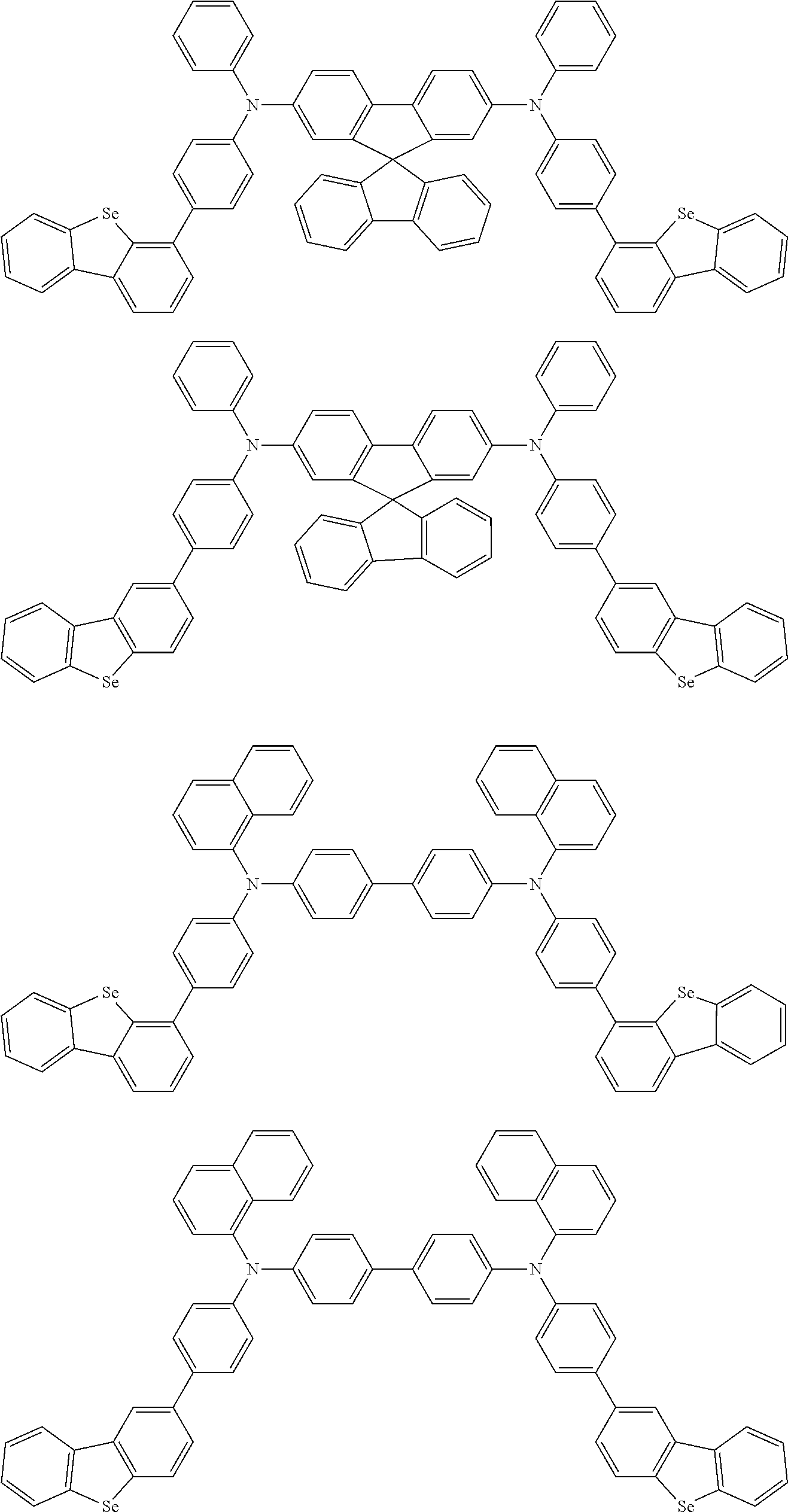


and derivatives thereof. Derivatives, such as compounds substituted by a substituent, including but not limited to halo, alkyl, heteroalkyl, cycloalkyl, alkenyl, alkynyl, arylkyl, heterocyclic group, aryl, and heteroaryl, are contemplated.

or a derivatives thereof, such as such as the compound substituted by a substituent, including but not limited to halo, alkyl heteroalkyl, cycloalkyl, alkenyl, alkynyl, arylkyl, heterocyclic group, aryl, and heteroaryl.


and derivative thereof. Derivatives, such compounds substituted by a substituent, including but not limited to halo, alkyl, heteroalkyl, cycloalkyl, alkenyl, alkynyl, arylkyl, heterocyclic group, aryl, and heteroaryl, are contemplated.
| TABLE 1 | ||
| MATE- | PUBLI- | |
| RIAL | EXAMPLES OF MATERIAL | CATIONS |
| Hole injection materials |
| Phthalo- cyanine and porph- ryrin com- pounds |
 |
Appl Phys. Lett. 69, 2160 (1996) |
| Star- burst triaryl- amines |
 |
J. Lumin. 72-74, 985 (1997) |
| CFx Fluoro- hydro- carbon polymer |
|
Appl. Phys. Lett. 78, 673 (2001) |
| Con- ducting poly- mers (e.g., PEDOT: PSS, poly- aniline, poly- pthio- phene) |
 |
Synth. Met. 87, 171 (1997) WO2007002683 |
| Phos- phonic acid and silane SAMs |
|
US20030162053 |
| Triaryl- amine or ploy- thio- phene poly- mers with con- duc- tivity dopants |
 |
EA01725079A1 |
 |
||
 |
||
| Aryl- amines com- plexed with metal oxides such as moly- bdenum and tung- sten oxides |
 |
SID Symposium Digest, 37, 923 (2006) WO2009018009 |
| p-type semi- con- ducting organic com- plexes |
 |
US20020158242 |
| Metal organo- metallic com- plexes |
 |
US20060240279 |
| Cross- linkable com- pounds |
 |
US20080220265 |
| Hole transporting materials |
| Tri- aryl- amines (e.g., TPD, α-NPD) |
 |
Appl. Phys. Lett. 51, 913 (1987) |
 |
U.S. Pat. No. 5,061,569 | |
 |
EP650955 | |
 |
J. Mater. Chem. 3, 319 (1993) | |
 |
Appl. Phys. Lett. 90, 183503 (2007) | |
 |
Appl. Phys. Lett. 90, 183503 (2007) | |
| Tri- aryl- amine on spiro- fluorene core |
 |
Synth. Met. 91, 209 (1997) |
| Aryl- amine carba- zole com- pounds |
 |
Adv. Mater. 6, 677 (1994), US20080124572 |
| Tri- aryl- amine with (di)- benzo- thio- phene/ (di)- benzo- furan |
 |
US20070278938, US20080106190 |
| Indo- lo- carba- zoles |
 |
Synth. Met. 111, 421 (2000) |
| Iso- indole com- pounds |
 |
Chem. Mater. 15, 3148 (2003) |
| Metal carbene com- plexes |
 |
US20080018221 |
| Phosphorescent OLED host materials |
| Red hosts |
| Aryl- car- bazoles |
 |
Appl. Phys. Lett. 78, 1622 (2001) |
| Metal 8- hydroxy- quino- lates (e.g., Alq3, BAlq) |
 |
Nature 395, 151 (1998) |
 |
US20060202194 | |
 |
WO2005014551 | |
 |
WO2006072002 | |
| Metal phen- oxy benzo- thi- azole com- pounds |
 |
Appl. Phys. Lett. 90, 123509 (2007) |
| Con- jugated oli- gomers and poly- mers (e.g., poly- fluorene) |
 |
Org. Electron. 1, 15 (2000) |
| Aro- matic fused rings |
 |
WO2009066779, WO2009066778, WO2009063833, US20090045731, US20090045730, WO2009008311, US20090008605, US20090009065 |
| Zinc com- plexes |
 |
WO2009062578 |
| Green hosts |
| Aryl- car- bazoles |
 |
Appl. Phys. Lett. 78, 1622 (2001) |
 |
US20030175553 | |
 |
WO2001039234 | |
| Aryl- tri- phenyl- ene com- pounds |
 |
US20060280965 |
 |
US20060280965 | |
 |
WO2009021126 | |
| Donor acceptor type mol- ecules |
 |
WO2008056746 |
| Aza- car- bazole/ DBT/ DBF |
 |
JP2008074939 |
| Poly- mers (e.g., PVK) |
 |
Appl. Phys. Lett. 77, 2280 (2000) |
| Spiro- fluorene com- pounds |
 |
WO2004093207 |
| Metal phen- oxy- benzo- oxazole com- pounds |
 |
WO2005089025 |
 |
WO2006132173 | |
 |
JP200511610 | |
| Spiro- fluorene- car- bazole com- pounds |
 |
JP2007254297 |
 |
JP2007254297 | |
| Indolo- car- bazoles |
 |
WO2007063796 |
 |
WO2007063754 | |
| 5- member ring electron de- ficient hetero- cycles (e.g., triazole, oxadi- azole) |
 |
J. Appl. Phys. 90, 5048 (2001) |
 |
WO2004107822 | |
| Tetra- phenyl- ene com- plexes |
 |
US20050112407 |
| Metal phenoxy- pyridine com- pounds |
 |
WO2005030900 |
| Metal coor- dination com- plexes (e.g., Zn, Al with N{circumflex over ( )}N ligands) |
 |
US20040137268, US20040137267 |
| Blue hosts |
| Aryl- car- bazoles |
 |
Appl. Phys. Lett, 82, 2422 (2003) |
 |
US20070190359 | |
| Dibenzo- thio- phene/ Dibenzo- furan- carba- zole com- pounds |
 |
WO2006114966, US20090167162 |
 |
US20090167162 | |
 |
WO2009086028 | |
 |
US20090030202, US20090017330 | |
| Silicon aryl com- pounds |
 |
US20050238919 |
 |
WO2009003898 | |
| Silicon/ German- ium aryl com- pounds |
 |
EP2034538A |
| Aryl benzoyl ester |
 |
WO2006100298 |
| High triplet metal organo- metallic com- plex |
 |
U.S. Pat. No. 7,154,114 |
| Phosphorescent dopants |
| Red dopants |
| Heavy metal por- phyrins (e.g., PtOEP) |
 |
Nature 395, 151 (1998) |
| Iridium (III) organo- metallic com- plexes |
 |
Appl. Phys. Lett. 78, 1622 (2001) |
 |
US2006835469 | |
 |
US2006835469 | |
 |
US20060202194 | |
 |
US20060202194 | |
 |
US20070087321 | |
 |
US20070087321 | |
 |
Adv. Mater. 19, 739 (2007) | |
 |
WO2009100991 | |
 |
WO2008101842 | |
| Platinum (II) organo- metallic com- plexes |
 |
WO2003040257 |
| Os- mium (III) com- plexes |
 |
Chem. Mater. 17, 3532 (2005) |
| Ruth- enium (II) com- plexes |
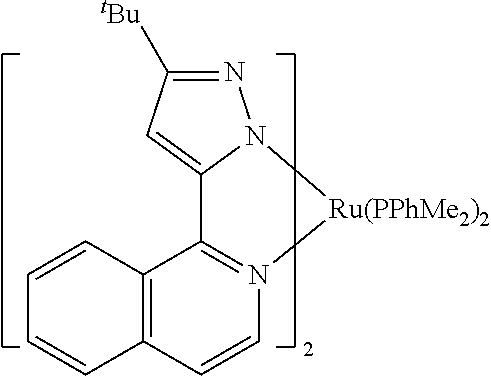 |
Adv. Mater. 17, 1059 (2005) |
| Rhe- nium (I), (II), and (III) com- plexes |
 |
US20050244673 |
| Green dopants |
| Iridium (III) organo- metallic com- plexes |
 |
Inorg. Chem. 40, 1704 (2001) |
| and its derivatives | ||
 |
US20020034656 | |
 |
U.S. Pat. No. 7,332,232 | |
 |
US20090108737 | |
 |
US20090039776 | |
 |
U.S. Pat. No. 6,921,915 | |
 |
U.S. Pat. No. 6,687,266 | |
 |
Chem. Mater. 16, 2480 (2004) | |
 |
US20070190359 | |
 |
US 20060008670 JP2007123392 | |
 |
Adv. Mater. 16, 2003 (2004) | |
 |
Angew. Chem. Int. Ed. 2006, 45, 7800 | |
 |
WO2009050290 | |
 |
US20090165846 | |
 |
US20080015355 | |
| Mon- omer for poly- meric metal organo- metallic com- pounds |
 |
U.S. Pat. No. 7,250,226, U.S. Pat. No. 7,396,598 |
| Pt(II) organo- metallic com- plexes, includ- ing poly- dentated ligands |
 |
Appl. Phys. Lett. 86, 153505 (2005) |
 |
Appl. Phys. Lett. 86, 153505 (2005) | |
 |
Chem. Lett. 34, 592 (2005) | |
 |
WO2002015645 | |
 |
US20060263635 | |
| Cu com- plexes |
 |
WO2009000673 |
| Gold com- plexes |
 |
Chem. Commun. 2906 (2005) |
| Rhe- nium (III) com- plexes |
 |
Inorg. Chem. 42, 1248 (2003) |
| Deuter- ated organo- metallic com- plexes |
 |
US20030138657 |
| Organo- metallic com- plexes with two or more metal centers |
 |
US20030152802 |
 |
U.S. Pat. No. 7,090,928 | |
| Blue dopants |
| Iridium (III) organo- metallic com- plexes |
 |
WO2002002714 |
 |
WO2006009024 | |
 |
US20060251923 | |
 |
U.S. Pat. No. 7,393,599, WO2006056418, US20050260441, WO2005019373 | |
 |
U.S. Pat. No. 7,534,505 | |
 |
U.S. Pat. No. 7,445,855 | |
 |
US20070190359, US20080297033 | |
 |
U.S. Pat. No. 7,338,722 | |
 |
US20020134984 | |
 |
Angew. Chem. Int. Ed. 47, 1 (2008) | |
 |
Chem. Mater. 18, 5119 (2006) | |
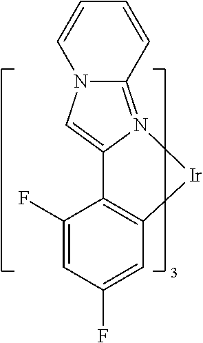 |
Inorg. Chem. 46, 4308 (2007) | |
 |
WO2005123873 | |
 |
WO2005123873 | |
 |
WO2007004380 | |
 |
WO2006082742 | |
| Osmium (II) com- plexes |
 |
U.S. Pat. No. 7,279,704 |
 |
Organo- metallics 23, 3745 (2004) | |
| Gold com- plexes |
|
Appl. Phys. Lett. 74, 1361 (1999) |
| Plat- inum (II) com- plexes |
 |
WO2006098120, WO2006103874 |
| Exciton/hole blocking layer materials |
| Bath- ocuprine com- pounds (e.g., BCP, BPhen) |
 |
Appl. Phys. Lett. 75, 4 (1999) |
 |
Appl. Phys. Lett. 79, 449 (2001) | |
| Metal 8- hydroxy- quin- olates (e.g., BAlq) |
 |
Appl. Phys. Lett. 81, 162 (2002) |
| 5- member ring electron deficient hetero- cycles such as triazole, oxadi- azole, imi- dazole, benzo- imi- dazole |
 |
Appl. Phys. Lett. 81, 162 (2002) |
| Tri- phenyl- ene com- pounds |
 |
US20050025993 |
| Fluor- inated aro- matic com- pounds |
 |
Appl. Phys. Lett. 79, 156 (2001) |
| Pheno- thia- zine- S- oxide |
 |
WO2008132085 |
| Electron transporting materials |
| Anthra- cene- benzo- imida- zole com- pounds |
 |
WO2003060956 |
 |
US20090179554 | |
| Aza tri- phenyl- ene deriva- tives |
 |
US20090115316 |
| An- thra- cene- benzo- thia- zole com- pounds |
 |
Appl. Phys. Lett. 89, 063504 (2006) |
| Metal 8- hydroxy- quino- lates (e.g., Alq3, Zrq4) |
 |
Appl. Phys. Lett. 51, 913 (1987) US7230107 |
| Metal hydroxy- beno- quin- olates |
 |
Chem. Lett. 5, 905 (1993) |
| Batho- cuprine com- pounds such as BCP, BPhen, etc |
 |
Appl. Phys. Lett. 91, 263503 (2007) |
 |
Appl. Phys. Lett. 79, 449 (2001) | |
| 5- member ring electron de- ficient hetero- cycles (e.g., triazole, oxadi- azole, imida- zole, benzo- imida- zole) |
 |
Appl. Phys. Lett. 74, 865 (1999) |
 |
Appl. Phys. Lett. 55, 1489 (1989) | |
 |
Jpn. J. Apply. Phys. 32, L917 (1993) | |
| Silole com- pounds |
 |
Org. Electron. 4, 113 (2003) |
| Aryl- borane com- pounds |
 |
J. Am. Chem. Soc. 120, 9714 (1998) |
| Fluor- inat- ed aro- matic com- pounds |
 |
J. Am. Chem. Soc. 122, 1832 (2000) |
| Full- erene (e.g., C60) |
 |
US20090101870 |
| Triazine com- plexes |
 |
US20040036077 |
| Zn (N{circumflex over ( )}N) com- plexes |
 |
U.S. Pat. No. 6,528,187 |


| TABLE 2 | ||||
| Device | ||||
| Example | Host | Dopant % | ETL2 (Å) | ETL1 (Å) |
| Comparative 1 | CBP | B 10% | HPT (50) | Alq3 (450) |
| Comparative 2 | CBP | A 10% | HPT (50) | Alq3 (450) |
| 1 | H-1 | A 10% | HPT (50) | Alq3 (450) |
| 2 | H-1 | A 10% | H-1 (100) | Alq3 (400) |
| 3 | H-1 | A 15% | HPT (50) | Alq3 (450) |
| 4 | H-1 | A 15% | H-1 (100) | Alq3 (400) |
| 5 | H-2 | A 10% | HPT (50) | Alq3 (450) |
| 6 | H-2 | A 10% | H-2 (100) | Alq3 (400) |
| 7 | H-2 | A 15% | HPT (50) | Alq3 (450) |
| 8 | H-2 | A 15% | H-2 (100) | Alq3 (400) |
| TABLE 3 | |||
| At L = 1000 cd/m2 | |||
| Device | CIE | V | LE | EQE | PE | At J = 40 mA/cm2 |
| Example | X | Y | (V) | (cd/A) | (%) | (lm/W) | Lo (cd/m2) | LTmax (hr) |
| Comparative 1 | 0.331 | 0.627 | 6.1 | 61.0 | 17 | 31.4 | 18,935 | 87 |
| Comparative 2 | 0.346 | 0.613 | 6.2 | 57.0 | 16 | 28.9 | 13,304 | 105 |
| 1 | 0.357 | 0.605 | 6.1 | 62.6 | 17.3 | 33.2 | 15,561 | 140 |
| 2 | 0.358 | 6.605 | 6.7 | 56.9 | 15.7 | 26.7 | 15,421 | 150 |
| 3 | 0.362 | 0.604 | 5.8 | 63.3 | 17.4 | 34.3 | 17,977 | 130 |
| 4 | 0.363 | 0.603 | 6.3 | 56.8 | 15.4 | 27.8 | 16,436 | 175 |
| 5 | 0.352 | 0.611 | 6.2 | 61.1 | 16.8 | 30.9 | 16,102 | 126 |
| 6 | 0.351 | 0.610 | 7.3 | 45.6 | 12.6 | 19.6 | 14,364 | 148 |
| 7 | 0.354 | 0.610 | 6.3 | 59.2 | 16.3 | 29.5 | 16,255 | 73 |
| 8 | 0.354 | 0.610 | 7.5 | 36.5 | 10 | 15.3 | 11,882 | 185 |
Claims (15)


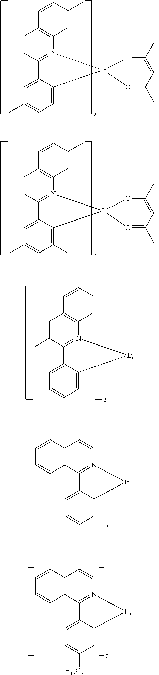


Priority Applications (1)
| Application Number | Priority Date | Filing Date | Title |
|---|---|---|---|
| US14/611,468 US9455411B2 (en) | 2008-09-25 | 2015-02-02 | Organic electroluminescent materials and devices |
Applications Claiming Priority (4)
| Application Number | Priority Date | Filing Date | Title |
|---|---|---|---|
| US10022908P | 2008-09-25 | 2008-09-25 | |
| US12/565,966 US8426035B2 (en) | 2008-09-25 | 2009-09-24 | Organoselenium materials and their uses in organic light emitting devices |
| US13/775,584 US8945727B2 (en) | 2008-09-25 | 2013-02-25 | Organoselenium materials and their uses in organic light emitting devices |
| US14/611,468 US9455411B2 (en) | 2008-09-25 | 2015-02-02 | Organic electroluminescent materials and devices |
Related Parent Applications (1)
| Application Number | Title | Priority Date | Filing Date |
|---|---|---|---|
| US13/775,584 Division US8945727B2 (en) | 2008-09-25 | 2013-02-25 | Organoselenium materials and their uses in organic light emitting devices |
Publications (2)
| Publication Number | Publication Date |
|---|---|
| US20150155499A1 US20150155499A1 (en) | 2015-06-04 |
| US9455411B2 true US9455411B2 (en) | 2016-09-27 |
Family
ID=41401827
Family Applications (3)
| Application Number | Title | Priority Date | Filing Date |
|---|---|---|---|
| US12/565,966 Active 2031-03-23 US8426035B2 (en) | 2008-09-25 | 2009-09-24 | Organoselenium materials and their uses in organic light emitting devices |
| US13/775,584 Active US8945727B2 (en) | 2008-09-25 | 2013-02-25 | Organoselenium materials and their uses in organic light emitting devices |
| US14/611,468 Active US9455411B2 (en) | 2008-09-25 | 2015-02-02 | Organic electroluminescent materials and devices |
Family Applications Before (2)
| Application Number | Title | Priority Date | Filing Date |
|---|---|---|---|
| US12/565,966 Active 2031-03-23 US8426035B2 (en) | 2008-09-25 | 2009-09-24 | Organoselenium materials and their uses in organic light emitting devices |
| US13/775,584 Active US8945727B2 (en) | 2008-09-25 | 2013-02-25 | Organoselenium materials and their uses in organic light emitting devices |
Country Status (7)
| Country | Link |
|---|---|
| US (3) | US8426035B2 (en) |
| EP (2) | EP2329540B1 (en) |
| JP (3) | JP5676454B2 (en) |
| KR (2) | KR101678235B1 (en) |
| CN (2) | CN103094490B (en) |
| TW (3) | TWI504596B (en) |
| WO (1) | WO2010036765A1 (en) |
Families Citing this family (31)
| Publication number | Priority date | Publication date | Assignee | Title |
|---|---|---|---|---|
| KR101678235B1 (en) * | 2008-09-25 | 2016-11-21 | 유니버셜 디스플레이 코포레이션 | Organoselenium materials and their uses in organic light emitting devices |
| JP5646733B2 (en) * | 2010-04-28 | 2014-12-24 | ユニバーサル ディスプレイ コーポレイション | Premixed material deposition |
| US8968887B2 (en) * | 2010-04-28 | 2015-03-03 | Universal Display Corporation | Triphenylene-benzofuran/benzothiophene/benzoselenophene compounds with substituents joining to form fused rings |
| JP5815341B2 (en) | 2010-09-09 | 2015-11-17 | 株式会社半導体エネルギー研究所 | Heterocyclic compounds |
| TWI558789B (en) * | 2010-10-11 | 2016-11-21 | 首威公司 | A spirobifluorene compound for light emitting devices |
| CN102558168B (en) * | 2010-12-23 | 2014-07-23 | 海洋王照明科技股份有限公司 | Organic semiconductor material and preparation method and application thereof |
| JP5959171B2 (en) * | 2011-09-08 | 2016-08-02 | 国立大学法人名古屋大学 | PI-conjugated organoboron compound and method for producing the same |
| EP2818464A4 (en) * | 2012-02-22 | 2015-11-18 | Jnc Corp | Novel chalcogen-containing organic compound and use thereof |
| JP5958988B2 (en) | 2012-03-16 | 2016-08-02 | Jnc株式会社 | Organic semiconductor thin film, organic semiconductor element, and organic field effect transistor |
| US9859517B2 (en) | 2012-09-07 | 2018-01-02 | Nitto Denko Corporation | White organic light-emitting diode |
| US9761807B2 (en) * | 2013-07-15 | 2017-09-12 | Universal Display Corporation | Organic light emitting diode materials |
| JP6388803B2 (en) * | 2013-07-22 | 2018-09-12 | 日本曹達株式会社 | Ruthenium complex |
| US9944846B2 (en) | 2014-08-28 | 2018-04-17 | E I Du Pont De Nemours And Company | Compositions for electronic applications |
| CN106032350B (en) * | 2015-03-09 | 2019-03-01 | 广东阿格蕾雅光电材料有限公司 | Organic electronic material |
| KR20160141931A (en) * | 2015-06-01 | 2016-12-12 | 삼성디스플레이 주식회사 | Organic light emitting diode and organic light emitting diode display including the same |
| CN104926785B (en) * | 2015-07-06 | 2018-10-09 | 盐城工学院 | A kind of selenium heteroaromatic ring derivative and preparation method thereof |
| JP6573979B2 (en) * | 2015-08-04 | 2019-09-11 | 富士フイルム株式会社 | Organic thin film transistor and manufacturing method thereof, organic thin film transistor material, organic thin film transistor composition, compound, and organic semiconductor film |
| US11522140B2 (en) * | 2015-08-17 | 2022-12-06 | Universal Display Corporation | Organic electroluminescent materials and devices |
| TWI565095B (en) * | 2015-11-09 | 2017-01-01 | 錼創科技股份有限公司 | Light emitting module |
| KR102455528B1 (en) * | 2015-11-24 | 2022-10-14 | 삼성전자주식회사 | Compound for organic photoelectric device and organic photoelectric device, image sensor and electronic device including the same |
| TW201829731A (en) * | 2016-11-04 | 2018-08-16 | 美商陶氏全球科技責任有限公司 | Composition containing aminium radical cation |
| WO2018085056A1 (en) * | 2016-11-04 | 2018-05-11 | Dow Global Technologies Llc | Organic light emitting diode containing aminium radical cation |
| JP6614370B2 (en) * | 2017-04-27 | 2019-12-04 | 住友化学株式会社 | Composition and light emitting device using the same |
| CN108178767B (en) * | 2018-01-19 | 2020-09-22 | 华南理工大学 | Organic small-molecule luminescent material based on pyrazine receptor unit and preparation method and application thereof |
| KR20200069400A (en) * | 2018-12-05 | 2020-06-17 | 삼성디스플레이 주식회사 | Condensed ring compound, composition including the same and organic light-emitting device including thin film formed therefrom |
| CN111333611B (en) * | 2018-12-19 | 2023-02-03 | 北京夏禾科技有限公司 | Organic electroluminescent material and device thereof |
| US11602724B2 (en) | 2019-04-30 | 2023-03-14 | Saint Louis University | Visible light induced photogeneration of ground state atomic oxygen |
| KR20230011859A (en) | 2021-07-14 | 2023-01-25 | 롬엔드하스전자재료코리아유한회사 | Organic electroluminescent compound and organic electroluminescent device comprising the same |
| DE102022119036A1 (en) | 2021-07-30 | 2023-02-02 | Rohm And Haas Electronic Materials Korea Ltd. | ORGANIC ELECTROLUMINESCENT COMPOUND, MULTIPLE HOST MATERIALS AND THIS COMPREHENSIVE ORGANIC ELECTROLUMINESCENT DEVICE |
| KR20230019014A (en) | 2021-07-30 | 2023-02-07 | 롬엔드하스전자재료코리아유한회사 | Organic electroluminescent compound, a plurality of host materials, and organic electroluminescent device comprising the same |
| KR20240039580A (en) | 2022-09-19 | 2024-03-26 | 롬엔드하스전자재료코리아유한회사 | A plurality of host materials, organic electroluminescent compound, and organic electroluminescent device comprising the same |
Citations (144)
| Publication number | Priority date | Publication date | Assignee | Title |
|---|---|---|---|---|
| EP0273643A2 (en) | 1986-12-18 | 1988-07-06 | The Regents Of The University Of California | Conducting substituted polyisothianophthenes |
| JPS63211265A (en) | 1987-02-27 | 1988-09-02 | Sds Biotech Kk | Tetracyanobenzene electric charge transfer complex |
| US4769292A (en) | 1987-03-02 | 1988-09-06 | Eastman Kodak Company | Electroluminescent device with modified thin film luminescent zone |
| US5061569A (en) | 1990-07-26 | 1991-10-29 | Eastman Kodak Company | Electroluminescent device with organic electroluminescent medium |
| US5121029A (en) | 1987-12-11 | 1992-06-09 | Idemitsu Kosan Co., Ltd. | Electroluminescence device having an organic electroluminescent element |
| US5130603A (en) | 1989-03-20 | 1992-07-14 | Idemitsu Kosan Co., Ltd. | Organic electroluminescence device |
| US5247190A (en) | 1989-04-20 | 1993-09-21 | Cambridge Research And Innovation Limited | Electroluminescent devices |
| JPH06212151A (en) | 1993-01-14 | 1994-08-02 | Toyo Ink Mfg Co Ltd | Organic electroluminescent element |
| EP0650955A1 (en) | 1993-11-01 | 1995-05-03 | Hodogaya Chemical Co., Ltd. | Amine compound and electro-luminescence device comprising same |
| JPH0753950Y2 (en) | 1990-11-06 | 1995-12-13 | シチズン時計株式会社 | Molded parts |
| US5703436A (en) | 1994-12-13 | 1997-12-30 | The Trustees Of Princeton University | Transparent contacts for organic devices |
| US5707745A (en) | 1994-12-13 | 1998-01-13 | The Trustees Of Princeton University | Multicolor organic light emitting devices |
| US5834893A (en) | 1996-12-23 | 1998-11-10 | The Trustees Of Princeton University | High efficiency organic light emitting devices with light directing structures |
| US5844363A (en) | 1997-01-23 | 1998-12-01 | The Trustees Of Princeton Univ. | Vacuum deposited, non-polymeric flexible organic light emitting devices |
| US6013982A (en) | 1996-12-23 | 2000-01-11 | The Trustees Of Princeton University | Multicolor display devices |
| US6087196A (en) | 1998-01-30 | 2000-07-11 | The Trustees Of Princeton University | Fabrication of organic semiconductor devices using ink jet printing |
| US6091195A (en) | 1997-02-03 | 2000-07-18 | The Trustees Of Princeton University | Displays having mesa pixel configuration |
| US6097147A (en) | 1998-09-14 | 2000-08-01 | The Trustees Of Princeton University | Structure for high efficiency electroluminescent device |
| JP2000252065A (en) | 1999-02-25 | 2000-09-14 | Sumitomo Chem Co Ltd | High molecular light emitting element |
| US6294398B1 (en) | 1999-11-23 | 2001-09-25 | The Trustees Of Princeton University | Method for patterning devices |
| US6303238B1 (en) | 1997-12-01 | 2001-10-16 | The Trustees Of Princeton University | OLEDs doped with phosphorescent compounds |
| US6310360B1 (en) | 1999-07-21 | 2001-10-30 | The Trustees Of Princeton University | Intersystem crossing agents for efficient utilization of excitons in organic light emitting devices |
| WO2001039234A3 (en) | 1999-11-24 | 2001-11-08 | Univ Princeton | Organic light emitting diode having a blue phosphorescent molecule as an emitter |
| US6337102B1 (en) | 1997-11-17 | 2002-01-08 | The Trustees Of Princeton University | Low pressure vapor phase deposition of organic thin films |
| WO2002015645A1 (en) | 2000-08-11 | 2002-02-21 | The Trustees Of Princeton University | Organometallic compounds and emission-shifting organic electrophosphorescence |
| US20020034656A1 (en) | 1998-09-14 | 2002-03-21 | Thompson Mark E. | Organometallic complexes as phosphorescent emitters in organic LEDs |
| US20020115079A1 (en) | 1996-10-03 | 2002-08-22 | Tadashi Okamoto | Process for detecting target nucleic acid, process for quantifying the same, and pyrylium compound for chemiluminescence analysis |
| WO2002074015A2 (en) | 2001-03-14 | 2002-09-19 | The Trustees Of Princeton University | Materials and devices for blue phosphorescence based organic light emitting diodes |
| US20020134984A1 (en) | 2001-02-01 | 2002-09-26 | Fuji Photo Film Co., Ltd. | Transition metal complex and light-emitting device |
| WO2002002714A3 (en) | 2000-06-30 | 2002-10-24 | Du Pont | Electroluminescent iridium compounds with fluorinated phenylpyridines, phenylpyrimidines, and phenylquinolines and devices made with such compounds |
| US20020158242A1 (en) | 1999-12-31 | 2002-10-31 | Se-Hwan Son | Electronic device comprising organic compound having p-type semiconducting characteristics |
| US20020182441A1 (en) | 2000-08-11 | 2002-12-05 | Trustee Of Princeton University | Organometallic compounds and emission-shifting organic electrophosphorescence |
| US6528187B1 (en) | 1998-09-08 | 2003-03-04 | Fuji Photo Film Co., Ltd. | Material for luminescence element and luminescence element using the same |
| US6548956B2 (en) | 1994-12-13 | 2003-04-15 | The Trustees Of Princeton University | Transparent contacts for organic devices |
| US20030072964A1 (en) | 2001-10-17 | 2003-04-17 | Kwong Raymond C. | Phosphorescent compounds and devices comprising the same |
| WO2003040257A1 (en) | 2001-11-07 | 2003-05-15 | E. I. Du Pont De Nemours And Company | Electroluminescent platinum compounds and devices made with such compounds |
| US6576134B1 (en) | 1998-10-20 | 2003-06-10 | Erik Agner | Method for displacement chromatography |
| US20030138657A1 (en) | 2000-12-07 | 2003-07-24 | Canon Kabushiki Kaisha | Deuterated semi-conducting organic compounds used for opto-electronic devices |
| US6602540B2 (en) | 1996-08-12 | 2003-08-05 | The Trustees Of Princeton University | Fabrication of non-polymeric flexible organic light emitting devices |
| US20030151042A1 (en) | 2002-02-08 | 2003-08-14 | Hueschen Mark R. | Polarization field enhanced tunnel structures |
| US20030152802A1 (en) | 2001-06-19 | 2003-08-14 | Akira Tsuboyama | Metal coordination compound and organic liminescence device |
| US20030175553A1 (en) | 2001-12-28 | 2003-09-18 | Thompson Mark E. | White light emitting oleds from combined monomer and aggregate emission |
| WO2003060956A3 (en) | 2002-01-18 | 2003-11-13 | Lg Chemical Ltd | New material for transporting electrons and organic electroluminescent display using the same |
| US20030230980A1 (en) | 2002-06-18 | 2003-12-18 | Forrest Stephen R | Very low voltage, high efficiency phosphorescent oled in a p-i-n structure |
| US6687266B1 (en) | 2002-11-08 | 2004-02-03 | Universal Display Corporation | Organic light emitting materials and devices |
| US20040036077A1 (en) | 2002-08-22 | 2004-02-26 | Fuji Photo Film Co., Ltd. | Light emitting element |
| US20040137267A1 (en) | 2002-12-27 | 2004-07-15 | Fuji Photo Film Co., Ltd. | Organic electroluminescent device |
| US20040137268A1 (en) | 2002-12-27 | 2004-07-15 | Fuji Photo Film Co., Ltd. | Organic electroluminescent device |
| US20040174116A1 (en) | 2001-08-20 | 2004-09-09 | Lu Min-Hao Michael | Transparent electrodes |
| WO2004107822A1 (en) | 2003-05-29 | 2004-12-09 | Nippon Steel Chemical Co., Ltd. | Organic electroluminescent element |
| JP2005011610A (en) | 2003-06-18 | 2005-01-13 | Nippon Steel Chem Co Ltd | Organic electroluminescent element |
| US20050025993A1 (en) | 2003-07-25 | 2005-02-03 | Thompson Mark E. | Materials and structures for enhancing the performance of organic light emitting devices |
| WO2005014551A1 (en) | 2003-08-07 | 2005-02-17 | Nippon Steel Chemical Co., Ltd. | Aluminum chelate compelx for organic el material |
| US6869695B2 (en) | 2001-12-28 | 2005-03-22 | The Trustees Of Princeton University | White light emitting OLEDs from combined monomer and aggregate emission |
| WO2005030900A1 (en) | 2003-09-25 | 2005-04-07 | Nippon Steel Chemical Co., Ltd. | Organic electroluminescent device |
| US20050079387A1 (en) | 2003-10-13 | 2005-04-14 | Seok-Jong Lee | Imidazole ring-containing compound and organic electroluminescence display device |
| WO2005019373A3 (en) | 2003-08-19 | 2005-05-19 | Basf Ag | Transition metal complexes comprising carbene ligands serving as emitters for organic light-emitting diodes (oled's) |
| US20050112407A1 (en) | 2003-11-21 | 2005-05-26 | Fuji Photo Film Co., Ltd. | Organic electroluminescent device |
| WO2004093207A3 (en) | 2003-04-15 | 2005-06-09 | Covion Organic Semiconductors | Mixtures of matrix materials and organic semiconductors capable of emission, use of the same and electronic components containing said mixtures |
| US6921915B2 (en) | 2001-03-08 | 2005-07-26 | Canon Kabushiki Kaisha | Metal coordination compound, luminescence device and display apparatus |
| WO2005089025A1 (en) | 2004-03-15 | 2005-09-22 | Nippon Steel Chemical Co., Ltd. | Organic electroluminescent device |
| US20050238919A1 (en) | 2004-04-23 | 2005-10-27 | Fuji Photo Film Co., Ltd. | Organic electroluminescent device |
| US20050244673A1 (en) | 2002-08-27 | 2005-11-03 | Fujitsu Limited | Organometallic complex, organic EL element and organic EL display |
| US20050260441A1 (en) | 2004-05-18 | 2005-11-24 | Thompson Mark E | Luminescent compounds with carbene ligands |
| US20050260449A1 (en) | 2004-05-18 | 2005-11-24 | Robert Walters | Complexes with tridentate ligands |
| WO2005123873A1 (en) | 2004-06-17 | 2005-12-29 | Konica Minolta Holdings, Inc. | Organic electroluminescent device material, organic electroluminescent device, display and illuminating device |
| US20060008670A1 (en) | 2004-07-06 | 2006-01-12 | Chun Lin | Organic light emitting materials and devices |
| WO2006009024A1 (en) | 2004-07-23 | 2006-01-26 | Konica Minolta Holdings, Inc. | Organic electroluminescent device, display and illuminating device |
| US7087321B2 (en) | 2003-04-22 | 2006-08-08 | Universal Display Corporation | Organic light emitting devices having reduced pixel shrinkage |
| WO2006082742A1 (en) | 2005-02-04 | 2006-08-10 | Konica Minolta Holdings, Inc. | Organic electroluminescent device material, organic electroluminescent device, display and illuminating device |
| US7090928B2 (en) | 2003-04-01 | 2006-08-15 | The University Of Southern California | Binuclear compounds |
| US20060202194A1 (en) | 2005-03-08 | 2006-09-14 | Jeong Hyun C | Red phosphorescene compounds and organic electroluminescence device using the same |
| WO2006098120A1 (en) | 2005-03-16 | 2006-09-21 | Konica Minolta Holdings, Inc. | Organic electroluminescent device material and organic electroluminescent device |
| WO2006100298A1 (en) | 2005-03-24 | 2006-09-28 | Basf Aktiengesellschaft | Use of compounds containing aromatic or heteroaromatic rings linked via carbonyl group-containing groups, for use as matrix materials in organic light-emitting diodes |
| US20060222886A1 (en) | 2005-04-04 | 2006-10-05 | Raymond Kwong | Arylpyrene compounds |
| WO2006103874A1 (en) | 2005-03-29 | 2006-10-05 | Konica Minolta Holdings, Inc. | Organic electroluminescent device material, organic electroluminescent device, display and illuminating device |
| US20060240279A1 (en) | 2005-04-21 | 2006-10-26 | Vadim Adamovich | Non-blocked phosphorescent OLEDs |
| WO2006114966A1 (en) | 2005-04-18 | 2006-11-02 | Konica Minolta Holdings, Inc. | Organic electroluminescent device, display and illuminating device |
| US20060251923A1 (en) | 2005-05-06 | 2006-11-09 | Chun Lin | Stability OLED materials and devices |
| EP1725079A1 (en) | 2004-03-11 | 2006-11-22 | Mitsubishi Chemical Corporation | Composition for charge-transporting film and ion compound, charge-transporting film and organic electroluminescent device using same, and method for manufacturing organic electroluminescent device and method for producing charge-transporting film |
| US20060263635A1 (en) | 2005-05-06 | 2006-11-23 | Fuji Photo Film Co., Ltd. | Organic electroluminescent device |
| US20060280965A1 (en) | 2005-05-31 | 2006-12-14 | Raymond Kwong | Triphenylene hosts in phosphorescent light emitting diodes |
| WO2006132173A1 (en) | 2005-06-07 | 2006-12-14 | Nippon Steel Chemical Co., Ltd. | Organic metal complex and organic electroluminescent device using same |
| US7154114B2 (en) | 2004-05-18 | 2006-12-26 | Universal Display Corporation | Cyclometallated iridium carbene complexes for use as hosts |
| WO2007004380A1 (en) | 2005-07-01 | 2007-01-11 | Konica Minolta Holdings, Inc. | Organic electroluminescent element material, organic electroluminescent element, display device, and lighting equipment |
| WO2006056418A8 (en) | 2004-11-25 | 2007-03-01 | Basf Ag | Use of transition metal carbene complexes in organic light-emitting diodes (oleds) |
| WO2006072002A3 (en) | 2004-12-30 | 2007-03-01 | Du Pont | Organometallic complexes |
| JP2007123392A (en) | 2005-10-26 | 2007-05-17 | Konica Minolta Holdings Inc | Organic electroluminescence device, display device and lighting device |
| WO2007063796A1 (en) | 2005-12-01 | 2007-06-07 | Nippon Steel Chemical Co., Ltd. | Organic electroluminescent device |
| WO2007063754A1 (en) | 2005-12-01 | 2007-06-07 | Nippon Steel Chemical Co., Ltd. | Compound for organic electroluminescent element and organic electroluminescent element |
| WO2007069569A1 (en) | 2005-12-15 | 2007-06-21 | Idemitsu Kosan Co., Ltd. | Organic electroluminescence element material and organic electroluminescence element using same |
| US7250226B2 (en) | 2001-08-31 | 2007-07-31 | Nippon Hoso Kyokai | Phosphorescent compound, a phosphorescent composition and an organic light-emitting device |
| US20070190359A1 (en) | 2006-02-10 | 2007-08-16 | Knowles David B | Metal complexes of cyclometallated imidazo[1,2-ƒ]phenanthridine and diimidazo[1,2-a:1',2'-c]quinazoline ligands and isoelectronic and benzannulated analogs thereof |
| WO2007002683A3 (en) | 2005-06-27 | 2007-09-20 | Du Pont | Electrically conductive polymer compositions |
| JP2007254297A (en) | 2006-03-20 | 2007-10-04 | Nippon Steel Chem Co Ltd | Compound of light-emitting layer and organic electroluminescent device |
| EP1847544A1 (en) | 2005-01-19 | 2007-10-24 | National University of Corporation Hiroshima University | Novel condensed polycyclic aromatic compound and use thereof |
| US20070278938A1 (en) | 2006-04-26 | 2007-12-06 | Idemitsu Kosan Co., Ltd. | Aromatic amine derivative and electroluminescence device using the same |
| US20080015355A1 (en) | 2004-06-28 | 2008-01-17 | Thomas Schafer | Electroluminescent Metal Complexes With Triazoles And Benzotriazoles |
| US7332232B2 (en) | 2004-02-03 | 2008-02-19 | Universal Display Corporation | OLEDs utilizing multidentate ligand systems |
| US7338722B2 (en) | 2003-03-24 | 2008-03-04 | The University Of Southern California | Phenyl and fluorenyl substituted phenyl-pyrazole complexes of Ir |
| EP1894923A1 (en) | 2005-06-24 | 2008-03-05 | Idemitsu Kosan Co., Ltd. | Benzothiophene derivative and organic electroluminescence device making use of the same |
| JP2008074939A (en) | 2006-09-21 | 2008-04-03 | Konica Minolta Holdings Inc | Organic electroluminescence element material, organic electroluminescence element, display device and illumination device |
| US20080100207A1 (en) | 2006-10-31 | 2008-05-01 | Sang-Hoon Park | Organoelectroluminescent compound and organoelectroluminescent device employing the same |
| US20080106190A1 (en) | 2006-08-23 | 2008-05-08 | Idemitsu Kosan Co., Ltd. | Aromatic amine derivatives and organic electroluminescent device using same |
| WO2008056746A1 (en) | 2006-11-09 | 2008-05-15 | Nippon Steel Chemical Co., Ltd. | Compound for organic electroluminescent device and organic electroluminescent device |
| US20080124572A1 (en) | 2006-11-24 | 2008-05-29 | Idemitsu Kosan Co., Ltd. | Aromatic amine derivative and organic electroluminescence device using the same |
| US7393599B2 (en) | 2004-05-18 | 2008-07-01 | The University Of Southern California | Luminescent compounds with carbene ligands |
| US7396598B2 (en) | 2001-06-20 | 2008-07-08 | Showa Denko K.K. | Light emitting material and organic light-emitting device |
| WO2008101842A1 (en) | 2007-02-23 | 2008-08-28 | Basf Se | Electroluminescent metal complexes with benzotriazoles |
| US20080220265A1 (en) | 2006-12-08 | 2008-09-11 | Universal Display Corporation | Cross-linkable Iridium Complexes and Organic Light-Emitting Devices Using the Same |
| US7431968B1 (en) | 2001-09-04 | 2008-10-07 | The Trustees Of Princeton University | Process and apparatus for organic vapor jet deposition |
| US7445855B2 (en) | 2004-05-18 | 2008-11-04 | The University Of Southern California | Cationic metal-carbene complexes |
| WO2008132085A1 (en) | 2007-04-26 | 2008-11-06 | Basf Se | Silanes containing phenothiazine-s-oxide or phenothiazine-s,s-dioxide groups and the use thereof in oleds |
| US20080297033A1 (en) | 2006-02-10 | 2008-12-04 | Knowles David B | Blue phosphorescent imidazophenanthridine materials |
| WO2009000673A2 (en) | 2007-06-22 | 2008-12-31 | Basf Se | Light emitting cu(i) complexes |
| US20090009065A1 (en) | 2007-07-07 | 2009-01-08 | Idemitsu Kosan Co., Ltd. | Organic electroluminescence device and material for organic electroluminescence device |
| US20090008605A1 (en) | 2007-07-07 | 2009-01-08 | Idemitsu Kosan Co., Ltd. | Naphthalene derivative, material for organic electroluminescence device, and organic electroluminescence device using the same |
| WO2009003898A1 (en) | 2007-07-05 | 2009-01-08 | Basf Se | Organic light-emitting diodes containing carbene transition metal complex emitters and at least one compound selected from disilylcarbazoles, disilyldibenzofurans, disilyldibenzothiophenes, disilyldibenzophospholes, disilyldibenzothiophene s-oxides and disilyldibenzothiophene s,s-dioxides |
| WO2009008311A1 (en) | 2007-07-07 | 2009-01-15 | Idemitsu Kosan Co., Ltd. | Chrysene derivative and organic electroluminescent device using the same |
| US20090017330A1 (en) | 2007-07-10 | 2009-01-15 | Idemitsu Kosan Co., Ltd. | Material for organic electroluminescence device and organic electroluminescence device utilizing the same |
| US20090030202A1 (en) | 2007-07-10 | 2009-01-29 | Idemitsu Kosan Co., Ltd. | Material for organic electroluminescent element and organic electroluminescent element employing the same |
| WO2009018009A1 (en) | 2007-07-27 | 2009-02-05 | E. I. Du Pont De Nemours And Company | Aqueous dispersions of electrically conducting polymers containing inorganic nanoparticles |
| WO2009021126A2 (en) | 2007-08-08 | 2009-02-12 | Universal Display Corporation | Benzo-fused thiophene or benzo-fused furan compounds comprising a triphenylene group |
| US20090039776A1 (en) | 2007-08-09 | 2009-02-12 | Canon Kabushiki Kaisha | Organometallic complex and organic light-emitting element using same |
| US20090045731A1 (en) | 2007-07-07 | 2009-02-19 | Idemitsu Kosan Co., Ltd. | Organic electroluminescence device and material for organic electroluminescence device |
| US20090045730A1 (en) | 2007-07-07 | 2009-02-19 | Idemitsu Kosan Co., Ltd. | Organic electroluminescence device and material for organic electroluminescence device |
| EP2034538A1 (en) | 2006-06-02 | 2009-03-11 | Idemitsu Kosan Co., Ltd. | Material for organic electroluminescence element, and organic electroluminescence element using the material |
| US20090101870A1 (en) | 2007-10-22 | 2009-04-23 | E. I. Du Pont De Nemours And Company | Electron transport bi-layers and devices made with such bi-layers |
| WO2009050290A1 (en) | 2007-10-17 | 2009-04-23 | Basf Se | Transition metal complexes having bridged carbene ligands and the use thereof in oleds |
| US20090108737A1 (en) | 2006-12-08 | 2009-04-30 | Raymond Kwong | Light-emitting organometallic complexes |
| US20090115316A1 (en) | 2007-11-02 | 2009-05-07 | Shiying Zheng | Organic electroluminescent device having an azatriphenylene derivative |
| US7534505B2 (en) | 2004-05-18 | 2009-05-19 | The University Of Southern California | Organometallic compounds for use in electroluminescent devices |
| WO2009063833A1 (en) | 2007-11-15 | 2009-05-22 | Idemitsu Kosan Co., Ltd. | Benzochrysene derivative and organic electroluminescent device using the same |
| WO2009062578A1 (en) | 2007-11-12 | 2009-05-22 | Merck Patent Gmbh | Organic electroluminescent devices comprising azomethine-metal complexes |
| WO2009066779A1 (en) | 2007-11-22 | 2009-05-28 | Idemitsu Kosan Co., Ltd. | Organic el element |
| WO2009066778A1 (en) | 2007-11-22 | 2009-05-28 | Idemitsu Kosan Co., Ltd. | Organic el element and solution containing organic el material |
| US20090165846A1 (en) | 2005-09-07 | 2009-07-02 | Universitaet Braunschweig | Triplet emitter having condensed five-membered rings |
| US20090167162A1 (en) | 2007-12-28 | 2009-07-02 | Universal Display Corporation | Dibenzothiophene-containing materials in phosphorescent light emitting diodes |
| WO2009086028A2 (en) | 2007-12-28 | 2009-07-09 | Universal Display Corporation | Carbazole-containing materials in phosphorescent light emitting diodes |
| US20090179554A1 (en) | 2006-05-11 | 2009-07-16 | Hitoshi Kuma | Organic electroluminescent device |
| WO2009100991A1 (en) | 2008-02-12 | 2009-08-20 | Basf Se | Electroluminescent metal complexes with dibenzo[f,h]quinoxalines |
| EP2101365A1 (en) | 2006-12-13 | 2009-09-16 | Konica Minolta Holdings, Inc. | Organic electroluminescent device, display and illuminating device |
| US8426035B2 (en) * | 2008-09-25 | 2013-04-23 | Universal Display Corporation | Organoselenium materials and their uses in organic light emitting devices |
| EP2239259B1 (en) | 2007-12-28 | 2016-04-13 | Idemitsu Kosan Co., Ltd. | Aromatic amine derivative and use of the same in an organic electroluminescent device |
Family Cites Families (14)
| Publication number | Priority date | Publication date | Assignee | Title |
|---|---|---|---|---|
| US222886A (en) * | 1879-12-23 | Improvement in automatic let-off mechanisms for looms | ||
| US34656A (en) * | 1862-03-11 | Improvement in liquids for exciting galvanic batteries | ||
| US174116A (en) * | 1876-02-29 | Improvement in car-couplings | ||
| US8010A (en) * | 1851-04-01 | Peter mckinlay | ||
| US280965A (en) * | 1883-07-10 | Map-drawing | ||
| US72964A (en) * | 1868-01-07 | Improved fire-kindling and fuel | ||
| US115079A (en) * | 1871-05-23 | Improvement in heating-stoves | ||
| US182441A (en) * | 1876-09-19 | Improvement in gold-foil condensers for dental use | ||
| US230980A (en) * | 1880-08-10 | Thomas e wobthlngto | ||
| JPH02263823A (en) * | 1989-04-04 | 1990-10-26 | Toyobo Co Ltd | Electrically conductive polymer |
| JP3114445B2 (en) * | 1993-08-10 | 2000-12-04 | 東洋インキ製造株式会社 | Organic electroluminescent device material and organic electroluminescent device using the same |
| JP3539221B2 (en) * | 1998-07-13 | 2004-07-07 | 豊田合成株式会社 | Resin molded product and method for producing the same |
| DE202005017678U1 (en) * | 2005-11-11 | 2007-03-22 | Seda S.P.A., Arzano | Box-shaped container and blank |
| WO2007105622A1 (en) * | 2006-03-10 | 2007-09-20 | National University Corporation Okayama University | Method for producing heterocyclic compound |
-
2009
- 2009-09-24 KR KR1020117005445A patent/KR101678235B1/en active IP Right Grant
- 2009-09-24 CN CN201310019226.1A patent/CN103094490B/en active Active
- 2009-09-24 EP EP09792929.3A patent/EP2329540B1/en active Active
- 2009-09-24 KR KR1020167017199A patent/KR101804084B1/en active IP Right Grant
- 2009-09-24 US US12/565,966 patent/US8426035B2/en active Active
- 2009-09-24 WO PCT/US2009/058162 patent/WO2010036765A1/en active Application Filing
- 2009-09-24 EP EP17150393.1A patent/EP3185333B1/en active Active
- 2009-09-24 CN CN200980136720.8A patent/CN102160206B/en active Active
- 2009-09-24 JP JP2011529209A patent/JP5676454B2/en active Active
- 2009-09-25 TW TW098132549A patent/TWI504596B/en active
- 2009-09-25 TW TW104108226A patent/TWI541237B/en active
- 2009-09-25 TW TW104123297A patent/TWI628173B/en active
-
2013
- 2013-02-25 US US13/775,584 patent/US8945727B2/en active Active
-
2014
- 2014-12-25 JP JP2014262199A patent/JP6067668B2/en active Active
-
2015
- 2015-02-02 US US14/611,468 patent/US9455411B2/en active Active
-
2016
- 2016-12-20 JP JP2016246367A patent/JP6506243B2/en active Active
Patent Citations (152)
| Publication number | Priority date | Publication date | Assignee | Title |
|---|---|---|---|---|
| EP0273643A2 (en) | 1986-12-18 | 1988-07-06 | The Regents Of The University Of California | Conducting substituted polyisothianophthenes |
| JPS63211265A (en) | 1987-02-27 | 1988-09-02 | Sds Biotech Kk | Tetracyanobenzene electric charge transfer complex |
| US4769292A (en) | 1987-03-02 | 1988-09-06 | Eastman Kodak Company | Electroluminescent device with modified thin film luminescent zone |
| US5121029A (en) | 1987-12-11 | 1992-06-09 | Idemitsu Kosan Co., Ltd. | Electroluminescence device having an organic electroluminescent element |
| US5130603A (en) | 1989-03-20 | 1992-07-14 | Idemitsu Kosan Co., Ltd. | Organic electroluminescence device |
| US5247190A (en) | 1989-04-20 | 1993-09-21 | Cambridge Research And Innovation Limited | Electroluminescent devices |
| US5061569A (en) | 1990-07-26 | 1991-10-29 | Eastman Kodak Company | Electroluminescent device with organic electroluminescent medium |
| JPH0753950Y2 (en) | 1990-11-06 | 1995-12-13 | シチズン時計株式会社 | Molded parts |
| JPH06212151A (en) | 1993-01-14 | 1994-08-02 | Toyo Ink Mfg Co Ltd | Organic electroluminescent element |
| EP0650955A1 (en) | 1993-11-01 | 1995-05-03 | Hodogaya Chemical Co., Ltd. | Amine compound and electro-luminescence device comprising same |
| US5703436A (en) | 1994-12-13 | 1997-12-30 | The Trustees Of Princeton University | Transparent contacts for organic devices |
| US5707745A (en) | 1994-12-13 | 1998-01-13 | The Trustees Of Princeton University | Multicolor organic light emitting devices |
| US6548956B2 (en) | 1994-12-13 | 2003-04-15 | The Trustees Of Princeton University | Transparent contacts for organic devices |
| US6602540B2 (en) | 1996-08-12 | 2003-08-05 | The Trustees Of Princeton University | Fabrication of non-polymeric flexible organic light emitting devices |
| US20020115079A1 (en) | 1996-10-03 | 2002-08-22 | Tadashi Okamoto | Process for detecting target nucleic acid, process for quantifying the same, and pyrylium compound for chemiluminescence analysis |
| US5834893A (en) | 1996-12-23 | 1998-11-10 | The Trustees Of Princeton University | High efficiency organic light emitting devices with light directing structures |
| US6013982A (en) | 1996-12-23 | 2000-01-11 | The Trustees Of Princeton University | Multicolor display devices |
| US5844363A (en) | 1997-01-23 | 1998-12-01 | The Trustees Of Princeton Univ. | Vacuum deposited, non-polymeric flexible organic light emitting devices |
| US6091195A (en) | 1997-02-03 | 2000-07-18 | The Trustees Of Princeton University | Displays having mesa pixel configuration |
| US6337102B1 (en) | 1997-11-17 | 2002-01-08 | The Trustees Of Princeton University | Low pressure vapor phase deposition of organic thin films |
| US6303238B1 (en) | 1997-12-01 | 2001-10-16 | The Trustees Of Princeton University | OLEDs doped with phosphorescent compounds |
| US6087196A (en) | 1998-01-30 | 2000-07-11 | The Trustees Of Princeton University | Fabrication of organic semiconductor devices using ink jet printing |
| US6528187B1 (en) | 1998-09-08 | 2003-03-04 | Fuji Photo Film Co., Ltd. | Material for luminescence element and luminescence element using the same |
| US20020034656A1 (en) | 1998-09-14 | 2002-03-21 | Thompson Mark E. | Organometallic complexes as phosphorescent emitters in organic LEDs |
| US6830828B2 (en) | 1998-09-14 | 2004-12-14 | The Trustees Of Princeton University | Organometallic complexes as phosphorescent emitters in organic LEDs |
| US6097147A (en) | 1998-09-14 | 2000-08-01 | The Trustees Of Princeton University | Structure for high efficiency electroluminescent device |
| US6576134B1 (en) | 1998-10-20 | 2003-06-10 | Erik Agner | Method for displacement chromatography |
| JP2000252065A (en) | 1999-02-25 | 2000-09-14 | Sumitomo Chem Co Ltd | High molecular light emitting element |
| US6310360B1 (en) | 1999-07-21 | 2001-10-30 | The Trustees Of Princeton University | Intersystem crossing agents for efficient utilization of excitons in organic light emitting devices |
| US6468819B1 (en) | 1999-11-23 | 2002-10-22 | The Trustees Of Princeton University | Method for patterning organic thin film devices using a die |
| US6294398B1 (en) | 1999-11-23 | 2001-09-25 | The Trustees Of Princeton University | Method for patterning devices |
| WO2001039234A3 (en) | 1999-11-24 | 2001-11-08 | Univ Princeton | Organic light emitting diode having a blue phosphorescent molecule as an emitter |
| US20020158242A1 (en) | 1999-12-31 | 2002-10-31 | Se-Hwan Son | Electronic device comprising organic compound having p-type semiconducting characteristics |
| WO2002002714A3 (en) | 2000-06-30 | 2002-10-24 | Du Pont | Electroluminescent iridium compounds with fluorinated phenylpyridines, phenylpyrimidines, and phenylquinolines and devices made with such compounds |
| US20020182441A1 (en) | 2000-08-11 | 2002-12-05 | Trustee Of Princeton University | Organometallic compounds and emission-shifting organic electrophosphorescence |
| WO2002015645A1 (en) | 2000-08-11 | 2002-02-21 | The Trustees Of Princeton University | Organometallic compounds and emission-shifting organic electrophosphorescence |
| US20030138657A1 (en) | 2000-12-07 | 2003-07-24 | Canon Kabushiki Kaisha | Deuterated semi-conducting organic compounds used for opto-electronic devices |
| US20020134984A1 (en) | 2001-02-01 | 2002-09-26 | Fuji Photo Film Co., Ltd. | Transition metal complex and light-emitting device |
| US6921915B2 (en) | 2001-03-08 | 2005-07-26 | Canon Kabushiki Kaisha | Metal coordination compound, luminescence device and display apparatus |
| WO2002074015A2 (en) | 2001-03-14 | 2002-09-19 | The Trustees Of Princeton University | Materials and devices for blue phosphorescence based organic light emitting diodes |
| US20030152802A1 (en) | 2001-06-19 | 2003-08-14 | Akira Tsuboyama | Metal coordination compound and organic liminescence device |
| US7396598B2 (en) | 2001-06-20 | 2008-07-08 | Showa Denko K.K. | Light emitting material and organic light-emitting device |
| US20040174116A1 (en) | 2001-08-20 | 2004-09-09 | Lu Min-Hao Michael | Transparent electrodes |
| US7250226B2 (en) | 2001-08-31 | 2007-07-31 | Nippon Hoso Kyokai | Phosphorescent compound, a phosphorescent composition and an organic light-emitting device |
| US7431968B1 (en) | 2001-09-04 | 2008-10-07 | The Trustees Of Princeton University | Process and apparatus for organic vapor jet deposition |
| US20030072964A1 (en) | 2001-10-17 | 2003-04-17 | Kwong Raymond C. | Phosphorescent compounds and devices comprising the same |
| US6835469B2 (en) | 2001-10-17 | 2004-12-28 | The University Of Southern California | Phosphorescent compounds and devices comprising the same |
| WO2003040257A1 (en) | 2001-11-07 | 2003-05-15 | E. I. Du Pont De Nemours And Company | Electroluminescent platinum compounds and devices made with such compounds |
| US20030175553A1 (en) | 2001-12-28 | 2003-09-18 | Thompson Mark E. | White light emitting oleds from combined monomer and aggregate emission |
| US6863997B2 (en) | 2001-12-28 | 2005-03-08 | The Trustees Of Princeton University | White light emitting OLEDs from combined monomer and aggregate emission |
| US6869695B2 (en) | 2001-12-28 | 2005-03-22 | The Trustees Of Princeton University | White light emitting OLEDs from combined monomer and aggregate emission |
| WO2003060956A3 (en) | 2002-01-18 | 2003-11-13 | Lg Chemical Ltd | New material for transporting electrons and organic electroluminescent display using the same |
| US20030151042A1 (en) | 2002-02-08 | 2003-08-14 | Hueschen Mark R. | Polarization field enhanced tunnel structures |
| US20030230980A1 (en) | 2002-06-18 | 2003-12-18 | Forrest Stephen R | Very low voltage, high efficiency phosphorescent oled in a p-i-n structure |
| US20040036077A1 (en) | 2002-08-22 | 2004-02-26 | Fuji Photo Film Co., Ltd. | Light emitting element |
| US20050244673A1 (en) | 2002-08-27 | 2005-11-03 | Fujitsu Limited | Organometallic complex, organic EL element and organic EL display |
| US6687266B1 (en) | 2002-11-08 | 2004-02-03 | Universal Display Corporation | Organic light emitting materials and devices |
| US20040137268A1 (en) | 2002-12-27 | 2004-07-15 | Fuji Photo Film Co., Ltd. | Organic electroluminescent device |
| US20040137267A1 (en) | 2002-12-27 | 2004-07-15 | Fuji Photo Film Co., Ltd. | Organic electroluminescent device |
| US7338722B2 (en) | 2003-03-24 | 2008-03-04 | The University Of Southern California | Phenyl and fluorenyl substituted phenyl-pyrazole complexes of Ir |
| US7090928B2 (en) | 2003-04-01 | 2006-08-15 | The University Of Southern California | Binuclear compounds |
| WO2004093207A3 (en) | 2003-04-15 | 2005-06-09 | Covion Organic Semiconductors | Mixtures of matrix materials and organic semiconductors capable of emission, use of the same and electronic components containing said mixtures |
| US7087321B2 (en) | 2003-04-22 | 2006-08-08 | Universal Display Corporation | Organic light emitting devices having reduced pixel shrinkage |
| WO2004107822A1 (en) | 2003-05-29 | 2004-12-09 | Nippon Steel Chemical Co., Ltd. | Organic electroluminescent element |
| JP2005011610A (en) | 2003-06-18 | 2005-01-13 | Nippon Steel Chem Co Ltd | Organic electroluminescent element |
| US20050025993A1 (en) | 2003-07-25 | 2005-02-03 | Thompson Mark E. | Materials and structures for enhancing the performance of organic light emitting devices |
| WO2005014551A1 (en) | 2003-08-07 | 2005-02-17 | Nippon Steel Chemical Co., Ltd. | Aluminum chelate compelx for organic el material |
| WO2005019373A3 (en) | 2003-08-19 | 2005-05-19 | Basf Ag | Transition metal complexes comprising carbene ligands serving as emitters for organic light-emitting diodes (oled's) |
| WO2005030900A1 (en) | 2003-09-25 | 2005-04-07 | Nippon Steel Chemical Co., Ltd. | Organic electroluminescent device |
| US20050079387A1 (en) | 2003-10-13 | 2005-04-14 | Seok-Jong Lee | Imidazole ring-containing compound and organic electroluminescence display device |
| US20050112407A1 (en) | 2003-11-21 | 2005-05-26 | Fuji Photo Film Co., Ltd. | Organic electroluminescent device |
| US7332232B2 (en) | 2004-02-03 | 2008-02-19 | Universal Display Corporation | OLEDs utilizing multidentate ligand systems |
| EP1725079A1 (en) | 2004-03-11 | 2006-11-22 | Mitsubishi Chemical Corporation | Composition for charge-transporting film and ion compound, charge-transporting film and organic electroluminescent device using same, and method for manufacturing organic electroluminescent device and method for producing charge-transporting film |
| WO2005089025A1 (en) | 2004-03-15 | 2005-09-22 | Nippon Steel Chemical Co., Ltd. | Organic electroluminescent device |
| US20050238919A1 (en) | 2004-04-23 | 2005-10-27 | Fuji Photo Film Co., Ltd. | Organic electroluminescent device |
| US7393599B2 (en) | 2004-05-18 | 2008-07-01 | The University Of Southern California | Luminescent compounds with carbene ligands |
| US7279704B2 (en) | 2004-05-18 | 2007-10-09 | The University Of Southern California | Complexes with tridentate ligands |
| US7445855B2 (en) | 2004-05-18 | 2008-11-04 | The University Of Southern California | Cationic metal-carbene complexes |
| US7534505B2 (en) | 2004-05-18 | 2009-05-19 | The University Of Southern California | Organometallic compounds for use in electroluminescent devices |
| US20050260449A1 (en) | 2004-05-18 | 2005-11-24 | Robert Walters | Complexes with tridentate ligands |
| US7154114B2 (en) | 2004-05-18 | 2006-12-26 | Universal Display Corporation | Cyclometallated iridium carbene complexes for use as hosts |
| US20050260441A1 (en) | 2004-05-18 | 2005-11-24 | Thompson Mark E | Luminescent compounds with carbene ligands |
| WO2005123873A1 (en) | 2004-06-17 | 2005-12-29 | Konica Minolta Holdings, Inc. | Organic electroluminescent device material, organic electroluminescent device, display and illuminating device |
| US20080015355A1 (en) | 2004-06-28 | 2008-01-17 | Thomas Schafer | Electroluminescent Metal Complexes With Triazoles And Benzotriazoles |
| US20060008670A1 (en) | 2004-07-06 | 2006-01-12 | Chun Lin | Organic light emitting materials and devices |
| WO2006009024A1 (en) | 2004-07-23 | 2006-01-26 | Konica Minolta Holdings, Inc. | Organic electroluminescent device, display and illuminating device |
| US20080018221A1 (en) | 2004-11-25 | 2008-01-24 | Basf Aktiengesellschaft | Use Of Transition Metal Carbene Complexes In Organic Light-Emitting Diodes (Oleds) |
| WO2006056418A8 (en) | 2004-11-25 | 2007-03-01 | Basf Ag | Use of transition metal carbene complexes in organic light-emitting diodes (oleds) |
| WO2006072002A3 (en) | 2004-12-30 | 2007-03-01 | Du Pont | Organometallic complexes |
| EP1847544A1 (en) | 2005-01-19 | 2007-10-24 | National University of Corporation Hiroshima University | Novel condensed polycyclic aromatic compound and use thereof |
| WO2006082742A1 (en) | 2005-02-04 | 2006-08-10 | Konica Minolta Holdings, Inc. | Organic electroluminescent device material, organic electroluminescent device, display and illuminating device |
| US20060202194A1 (en) | 2005-03-08 | 2006-09-14 | Jeong Hyun C | Red phosphorescene compounds and organic electroluminescence device using the same |
| WO2006098120A1 (en) | 2005-03-16 | 2006-09-21 | Konica Minolta Holdings, Inc. | Organic electroluminescent device material and organic electroluminescent device |
| WO2006100298A1 (en) | 2005-03-24 | 2006-09-28 | Basf Aktiengesellschaft | Use of compounds containing aromatic or heteroaromatic rings linked via carbonyl group-containing groups, for use as matrix materials in organic light-emitting diodes |
| WO2006103874A1 (en) | 2005-03-29 | 2006-10-05 | Konica Minolta Holdings, Inc. | Organic electroluminescent device material, organic electroluminescent device, display and illuminating device |
| US20060222886A1 (en) | 2005-04-04 | 2006-10-05 | Raymond Kwong | Arylpyrene compounds |
| WO2006114966A1 (en) | 2005-04-18 | 2006-11-02 | Konica Minolta Holdings, Inc. | Organic electroluminescent device, display and illuminating device |
| US20060240279A1 (en) | 2005-04-21 | 2006-10-26 | Vadim Adamovich | Non-blocked phosphorescent OLEDs |
| US20060263635A1 (en) | 2005-05-06 | 2006-11-23 | Fuji Photo Film Co., Ltd. | Organic electroluminescent device |
| US20060251923A1 (en) | 2005-05-06 | 2006-11-09 | Chun Lin | Stability OLED materials and devices |
| US20060280965A1 (en) | 2005-05-31 | 2006-12-14 | Raymond Kwong | Triphenylene hosts in phosphorescent light emitting diodes |
| WO2006132173A1 (en) | 2005-06-07 | 2006-12-14 | Nippon Steel Chemical Co., Ltd. | Organic metal complex and organic electroluminescent device using same |
| EP1894923A1 (en) | 2005-06-24 | 2008-03-05 | Idemitsu Kosan Co., Ltd. | Benzothiophene derivative and organic electroluminescence device making use of the same |
| WO2007002683A3 (en) | 2005-06-27 | 2007-09-20 | Du Pont | Electrically conductive polymer compositions |
| WO2007004380A1 (en) | 2005-07-01 | 2007-01-11 | Konica Minolta Holdings, Inc. | Organic electroluminescent element material, organic electroluminescent element, display device, and lighting equipment |
| US20090165846A1 (en) | 2005-09-07 | 2009-07-02 | Universitaet Braunschweig | Triplet emitter having condensed five-membered rings |
| JP2007123392A (en) | 2005-10-26 | 2007-05-17 | Konica Minolta Holdings Inc | Organic electroluminescence device, display device and lighting device |
| WO2007063754A1 (en) | 2005-12-01 | 2007-06-07 | Nippon Steel Chemical Co., Ltd. | Compound for organic electroluminescent element and organic electroluminescent element |
| WO2007063796A1 (en) | 2005-12-01 | 2007-06-07 | Nippon Steel Chemical Co., Ltd. | Organic electroluminescent device |
| WO2007069569A1 (en) | 2005-12-15 | 2007-06-21 | Idemitsu Kosan Co., Ltd. | Organic electroluminescence element material and organic electroluminescence element using same |
| EP1962354A1 (en) | 2005-12-15 | 2008-08-27 | Idemitsu Kosan Co., Ltd. | Organic electroluminescence element material and organic electroluminescence element using same |
| US20080297033A1 (en) | 2006-02-10 | 2008-12-04 | Knowles David B | Blue phosphorescent imidazophenanthridine materials |
| US20070190359A1 (en) | 2006-02-10 | 2007-08-16 | Knowles David B | Metal complexes of cyclometallated imidazo[1,2-ƒ]phenanthridine and diimidazo[1,2-a:1',2'-c]quinazoline ligands and isoelectronic and benzannulated analogs thereof |
| JP2007254297A (en) | 2006-03-20 | 2007-10-04 | Nippon Steel Chem Co Ltd | Compound of light-emitting layer and organic electroluminescent device |
| US20070278938A1 (en) | 2006-04-26 | 2007-12-06 | Idemitsu Kosan Co., Ltd. | Aromatic amine derivative and electroluminescence device using the same |
| US20090179554A1 (en) | 2006-05-11 | 2009-07-16 | Hitoshi Kuma | Organic electroluminescent device |
| EP2034538A1 (en) | 2006-06-02 | 2009-03-11 | Idemitsu Kosan Co., Ltd. | Material for organic electroluminescence element, and organic electroluminescence element using the material |
| US20080106190A1 (en) | 2006-08-23 | 2008-05-08 | Idemitsu Kosan Co., Ltd. | Aromatic amine derivatives and organic electroluminescent device using same |
| JP2008074939A (en) | 2006-09-21 | 2008-04-03 | Konica Minolta Holdings Inc | Organic electroluminescence element material, organic electroluminescence element, display device and illumination device |
| KR20080039057A (en) | 2006-10-31 | 2008-05-07 | 삼성에스디아이 주식회사 | Organoelectroluminescent compound and organoelectroluminescent device employing the same |
| US20080100207A1 (en) | 2006-10-31 | 2008-05-01 | Sang-Hoon Park | Organoelectroluminescent compound and organoelectroluminescent device employing the same |
| WO2008056746A1 (en) | 2006-11-09 | 2008-05-15 | Nippon Steel Chemical Co., Ltd. | Compound for organic electroluminescent device and organic electroluminescent device |
| US20080124572A1 (en) | 2006-11-24 | 2008-05-29 | Idemitsu Kosan Co., Ltd. | Aromatic amine derivative and organic electroluminescence device using the same |
| US20080220265A1 (en) | 2006-12-08 | 2008-09-11 | Universal Display Corporation | Cross-linkable Iridium Complexes and Organic Light-Emitting Devices Using the Same |
| US20090108737A1 (en) | 2006-12-08 | 2009-04-30 | Raymond Kwong | Light-emitting organometallic complexes |
| EP2101365A1 (en) | 2006-12-13 | 2009-09-16 | Konica Minolta Holdings, Inc. | Organic electroluminescent device, display and illuminating device |
| WO2008101842A1 (en) | 2007-02-23 | 2008-08-28 | Basf Se | Electroluminescent metal complexes with benzotriazoles |
| WO2008132085A1 (en) | 2007-04-26 | 2008-11-06 | Basf Se | Silanes containing phenothiazine-s-oxide or phenothiazine-s,s-dioxide groups and the use thereof in oleds |
| WO2009000673A2 (en) | 2007-06-22 | 2008-12-31 | Basf Se | Light emitting cu(i) complexes |
| WO2009003898A1 (en) | 2007-07-05 | 2009-01-08 | Basf Se | Organic light-emitting diodes containing carbene transition metal complex emitters and at least one compound selected from disilylcarbazoles, disilyldibenzofurans, disilyldibenzothiophenes, disilyldibenzophospholes, disilyldibenzothiophene s-oxides and disilyldibenzothiophene s,s-dioxides |
| WO2009008311A1 (en) | 2007-07-07 | 2009-01-15 | Idemitsu Kosan Co., Ltd. | Chrysene derivative and organic electroluminescent device using the same |
| US20090008605A1 (en) | 2007-07-07 | 2009-01-08 | Idemitsu Kosan Co., Ltd. | Naphthalene derivative, material for organic electroluminescence device, and organic electroluminescence device using the same |
| US20090045731A1 (en) | 2007-07-07 | 2009-02-19 | Idemitsu Kosan Co., Ltd. | Organic electroluminescence device and material for organic electroluminescence device |
| US20090045730A1 (en) | 2007-07-07 | 2009-02-19 | Idemitsu Kosan Co., Ltd. | Organic electroluminescence device and material for organic electroluminescence device |
| US20090009065A1 (en) | 2007-07-07 | 2009-01-08 | Idemitsu Kosan Co., Ltd. | Organic electroluminescence device and material for organic electroluminescence device |
| US20090017330A1 (en) | 2007-07-10 | 2009-01-15 | Idemitsu Kosan Co., Ltd. | Material for organic electroluminescence device and organic electroluminescence device utilizing the same |
| US20090030202A1 (en) | 2007-07-10 | 2009-01-29 | Idemitsu Kosan Co., Ltd. | Material for organic electroluminescent element and organic electroluminescent element employing the same |
| WO2009018009A1 (en) | 2007-07-27 | 2009-02-05 | E. I. Du Pont De Nemours And Company | Aqueous dispersions of electrically conducting polymers containing inorganic nanoparticles |
| WO2009021126A2 (en) | 2007-08-08 | 2009-02-12 | Universal Display Corporation | Benzo-fused thiophene or benzo-fused furan compounds comprising a triphenylene group |
| US20090039776A1 (en) | 2007-08-09 | 2009-02-12 | Canon Kabushiki Kaisha | Organometallic complex and organic light-emitting element using same |
| WO2009050290A1 (en) | 2007-10-17 | 2009-04-23 | Basf Se | Transition metal complexes having bridged carbene ligands and the use thereof in oleds |
| US20090101870A1 (en) | 2007-10-22 | 2009-04-23 | E. I. Du Pont De Nemours And Company | Electron transport bi-layers and devices made with such bi-layers |
| US20090115316A1 (en) | 2007-11-02 | 2009-05-07 | Shiying Zheng | Organic electroluminescent device having an azatriphenylene derivative |
| WO2009062578A1 (en) | 2007-11-12 | 2009-05-22 | Merck Patent Gmbh | Organic electroluminescent devices comprising azomethine-metal complexes |
| WO2009063833A1 (en) | 2007-11-15 | 2009-05-22 | Idemitsu Kosan Co., Ltd. | Benzochrysene derivative and organic electroluminescent device using the same |
| WO2009066779A1 (en) | 2007-11-22 | 2009-05-28 | Idemitsu Kosan Co., Ltd. | Organic el element |
| WO2009066778A1 (en) | 2007-11-22 | 2009-05-28 | Idemitsu Kosan Co., Ltd. | Organic el element and solution containing organic el material |
| US20090167162A1 (en) | 2007-12-28 | 2009-07-02 | Universal Display Corporation | Dibenzothiophene-containing materials in phosphorescent light emitting diodes |
| WO2009086028A2 (en) | 2007-12-28 | 2009-07-09 | Universal Display Corporation | Carbazole-containing materials in phosphorescent light emitting diodes |
| EP2239259B1 (en) | 2007-12-28 | 2016-04-13 | Idemitsu Kosan Co., Ltd. | Aromatic amine derivative and use of the same in an organic electroluminescent device |
| WO2009100991A1 (en) | 2008-02-12 | 2009-08-20 | Basf Se | Electroluminescent metal complexes with dibenzo[f,h]quinoxalines |
| US8426035B2 (en) * | 2008-09-25 | 2013-04-23 | Universal Display Corporation | Organoselenium materials and their uses in organic light emitting devices |
Non-Patent Citations (79)
Also Published As
| Publication number | Publication date |
|---|---|
| TWI504596B (en) | 2015-10-21 |
| TW201522324A (en) | 2015-06-16 |
| KR20160078526A (en) | 2016-07-04 |
| US20130168660A1 (en) | 2013-07-04 |
| JP5676454B2 (en) | 2015-02-25 |
| US20150155499A1 (en) | 2015-06-04 |
| JP6067668B2 (en) | 2017-01-25 |
| CN103094490A (en) | 2013-05-08 |
| KR101804084B1 (en) | 2017-12-01 |
| JP2012503889A (en) | 2012-02-09 |
| JP2017098556A (en) | 2017-06-01 |
| KR101678235B1 (en) | 2016-11-21 |
| CN103094490B (en) | 2016-03-09 |
| TWI541237B (en) | 2016-07-11 |
| EP3185333B1 (en) | 2023-09-06 |
| CN102160206B (en) | 2014-06-11 |
| WO2010036765A1 (en) | 2010-04-01 |
| EP3185333A2 (en) | 2017-06-28 |
| TWI628173B (en) | 2018-07-01 |
| EP3185333A3 (en) | 2017-10-04 |
| US20100072887A1 (en) | 2010-03-25 |
| TW201022224A (en) | 2010-06-16 |
| TW201538493A (en) | 2015-10-16 |
| JP2015119186A (en) | 2015-06-25 |
| CN102160206A (en) | 2011-08-17 |
| US8426035B2 (en) | 2013-04-23 |
| KR20110071061A (en) | 2011-06-28 |
| EP2329540A1 (en) | 2011-06-08 |
| JP6506243B2 (en) | 2019-04-24 |
| US8945727B2 (en) | 2015-02-03 |
| EP2329540B1 (en) | 2017-01-11 |
Similar Documents
| Publication | Publication Date | Title |
|---|---|---|
| US9455411B2 (en) | Organic electroluminescent materials and devices | |
| US20220216421A1 (en) | Organic electroluminescent materials and devices | |
| US9997726B2 (en) | Dibenzothiophene-containing materials in phosphorescent light emitting diodes | |
| US9401482B2 (en) | Organic electroluminescent materials and devices | |
| US9847495B2 (en) | Organic electroluminescent materials and devices | |
| US8415031B2 (en) | Electron transporting compounds | |
| US8968887B2 (en) | Triphenylene-benzofuran/benzothiophene/benzoselenophene compounds with substituents joining to form fused rings | |
| US8722205B2 (en) | Heteroleptic iridium complex | |
| US9142788B2 (en) | Host materials for OLEDs | |
| US9184399B2 (en) | Asymmetric hosts with triaryl silane side chains | |
| US20130026909A1 (en) | Host materials for phosphorescent oleds | |
| US9118017B2 (en) | Host compounds for red phosphorescent OLEDs | |
| US20160315269A1 (en) | Organic electroluminescent materials and devices |
Legal Events
| Date | Code | Title | Description |
|---|---|---|---|
| AS | Assignment |
Owner name: UNIVERSAL DISPLAY CORPORATION, NEW JERSEY Free format text: ASSIGNMENT OF ASSIGNORS INTEREST;ASSIGNORS:KWONG, RAYMOND;MA, BIN;XIA, CHUANJUN;AND OTHERS;SIGNING DATES FROM 20091005 TO 20091014;REEL/FRAME:034865/0800 |
|
| FEPP | Fee payment procedure |
Free format text: PAYOR NUMBER ASSIGNED (ORIGINAL EVENT CODE: ASPN); ENTITY STATUS OF PATENT OWNER: LARGE ENTITY |
|
| STCF | Information on status: patent grant |
Free format text: PATENTED CASE |
|
| CC | Certificate of correction | ||
| MAFP | Maintenance fee payment |
Free format text: PAYMENT OF MAINTENANCE FEE, 4TH YEAR, LARGE ENTITY (ORIGINAL EVENT CODE: M1551); ENTITY STATUS OF PATENT OWNER: LARGE ENTITY Year of fee payment: 4 |
|
| MAFP | Maintenance fee payment |
Free format text: PAYMENT OF MAINTENANCE FEE, 8TH YEAR, LARGE ENTITY (ORIGINAL EVENT CODE: M1552); ENTITY STATUS OF PATENT OWNER: LARGE ENTITY Year of fee payment: 8 |