US9468750B2 - Multilayer planar spiral inductor filter for medical therapeutic or diagnostic applications - Google Patents
Multilayer planar spiral inductor filter for medical therapeutic or diagnostic applications Download PDFInfo
- Publication number
- US9468750B2 US9468750B2 US13/958,604 US201313958604A US9468750B2 US 9468750 B2 US9468750 B2 US 9468750B2 US 201313958604 A US201313958604 A US 201313958604A US 9468750 B2 US9468750 B2 US 9468750B2
- Authority
- US
- United States
- Prior art keywords
- spiral
- dielectric substrate
- inductor
- implantable lead
- lead
- Prior art date
- Legal status (The legal status is an assumption and is not a legal conclusion. Google has not performed a legal analysis and makes no representation as to the accuracy of the status listed.)
- Expired - Fee Related, expires
Links
- 230000001225 therapeutic effect Effects 0.000 title abstract description 5
- 239000004020 conductor Substances 0.000 claims abstract description 131
- 239000003989 dielectric material Substances 0.000 claims abstract description 22
- 230000001939 inductive effect Effects 0.000 claims abstract description 19
- 239000000758 substrate Substances 0.000 claims description 52
- 230000003071 parasitic effect Effects 0.000 claims description 47
- 238000000034 method Methods 0.000 claims description 30
- 239000000463 material Substances 0.000 claims description 24
- 230000008569 process Effects 0.000 claims description 15
- -1 polytetrafluoroethylene Polymers 0.000 claims description 11
- 229920000642 polymer Polymers 0.000 claims description 9
- 229920001343 polytetrafluoroethylene Polymers 0.000 claims description 9
- 239000004810 polytetrafluoroethylene Substances 0.000 claims description 9
- VYPSYNLAJGMNEJ-UHFFFAOYSA-N Silicium dioxide Chemical compound O=[Si]=O VYPSYNLAJGMNEJ-UHFFFAOYSA-N 0.000 claims description 8
- 229920006362 Teflon® Polymers 0.000 claims description 8
- 229920000840 ethylene tetrafluoroethylene copolymer Polymers 0.000 claims description 8
- 239000000835 fiber Substances 0.000 claims description 8
- 239000004952 Polyamide Substances 0.000 claims description 7
- 239000004642 Polyimide Substances 0.000 claims description 7
- GWEVSGVZZGPLCZ-UHFFFAOYSA-N Titan oxide Chemical compound O=[Ti]=O GWEVSGVZZGPLCZ-UHFFFAOYSA-N 0.000 claims description 7
- 229920002647 polyamide Polymers 0.000 claims description 7
- 229920001721 polyimide Polymers 0.000 claims description 7
- 239000004696 Poly ether ether ketone Substances 0.000 claims description 6
- 229910003460 diamond Inorganic materials 0.000 claims description 6
- 239000010432 diamond Substances 0.000 claims description 6
- 229920002120 photoresistant polymer Polymers 0.000 claims description 6
- 229920000052 poly(p-xylylene) Polymers 0.000 claims description 6
- 229920002530 polyetherether ketone Polymers 0.000 claims description 6
- 229920000139 polyethylene terephthalate Polymers 0.000 claims description 6
- 239000005020 polyethylene terephthalate Substances 0.000 claims description 6
- RTAQQCXQSZGOHL-UHFFFAOYSA-N Titanium Chemical compound [Ti] RTAQQCXQSZGOHL-UHFFFAOYSA-N 0.000 claims description 5
- 239000000560 biocompatible material Substances 0.000 claims description 5
- 229920001296 polysiloxane Polymers 0.000 claims description 5
- 229910052719 titanium Inorganic materials 0.000 claims description 5
- 239000010936 titanium Substances 0.000 claims description 5
- VTYYLEPIZMXCLO-UHFFFAOYSA-L Calcium carbonate Chemical compound [Ca+2].[O-]C([O-])=O VTYYLEPIZMXCLO-UHFFFAOYSA-L 0.000 claims description 4
- 229920002614 Polyether block amide Polymers 0.000 claims description 4
- 239000004743 Polypropylene Substances 0.000 claims description 4
- 229910052581 Si3N4 Inorganic materials 0.000 claims description 4
- 229910002113 barium titanate Inorganic materials 0.000 claims description 4
- TWNQGVIAIRXVLR-UHFFFAOYSA-N oxo(oxoalumanyloxy)alumane Chemical compound O=[Al]O[Al]=O TWNQGVIAIRXVLR-UHFFFAOYSA-N 0.000 claims description 4
- BPUBBGLMJRNUCC-UHFFFAOYSA-N oxygen(2-);tantalum(5+) Chemical compound [O-2].[O-2].[O-2].[O-2].[O-2].[Ta+5].[Ta+5] BPUBBGLMJRNUCC-UHFFFAOYSA-N 0.000 claims description 4
- 239000002245 particle Substances 0.000 claims description 4
- 229920001155 polypropylene Polymers 0.000 claims description 4
- HQVNEWCFYHHQES-UHFFFAOYSA-N silicon nitride Chemical compound N12[Si]34N5[Si]62N3[Si]51N64 HQVNEWCFYHHQES-UHFFFAOYSA-N 0.000 claims description 4
- 229910052814 silicon oxide Inorganic materials 0.000 claims description 4
- 239000004593 Epoxy Substances 0.000 claims description 3
- 229920000249 biocompatible polymer Polymers 0.000 claims description 3
- 239000002131 composite material Substances 0.000 claims description 3
- 229920001971 elastomer Polymers 0.000 claims description 3
- 239000000806 elastomer Substances 0.000 claims description 3
- 238000005530 etching Methods 0.000 claims description 3
- 238000001704 evaporation Methods 0.000 claims description 3
- 230000008020 evaporation Effects 0.000 claims description 3
- 239000000499 gel Substances 0.000 claims description 3
- 230000001788 irregular Effects 0.000 claims description 3
- 239000004800 polyvinyl chloride Substances 0.000 claims description 3
- 238000004528 spin coating Methods 0.000 claims description 3
- 229910052715 tantalum Inorganic materials 0.000 claims description 3
- GUVRBAGPIYLISA-UHFFFAOYSA-N tantalum atom Chemical compound [Ta] GUVRBAGPIYLISA-UHFFFAOYSA-N 0.000 claims description 3
- 229920002595 Dielectric elastomer Polymers 0.000 claims description 2
- 239000004677 Nylon Substances 0.000 claims description 2
- 239000004793 Polystyrene Substances 0.000 claims description 2
- NRTOMJZYCJJWKI-UHFFFAOYSA-N Titanium nitride Chemical compound [Ti]#N NRTOMJZYCJJWKI-UHFFFAOYSA-N 0.000 claims description 2
- VXAUWWUXCIMFIM-UHFFFAOYSA-M aluminum;oxygen(2-);hydroxide Chemical compound [OH-].[O-2].[Al+3] VXAUWWUXCIMFIM-UHFFFAOYSA-M 0.000 claims description 2
- JRPBQTZRNDNNOP-UHFFFAOYSA-N barium titanate Chemical compound [Ba+2].[Ba+2].[O-][Ti]([O-])([O-])[O-] JRPBQTZRNDNNOP-UHFFFAOYSA-N 0.000 claims description 2
- 229910000019 calcium carbonate Inorganic materials 0.000 claims description 2
- 239000003575 carbonaceous material Substances 0.000 claims description 2
- 229920001577 copolymer Polymers 0.000 claims description 2
- 125000003700 epoxy group Chemical group 0.000 claims description 2
- CJNBYAVZURUTKZ-UHFFFAOYSA-N hafnium(iv) oxide Chemical compound O=[Hf]=O CJNBYAVZURUTKZ-UHFFFAOYSA-N 0.000 claims description 2
- 239000010445 mica Substances 0.000 claims description 2
- 229910052618 mica group Inorganic materials 0.000 claims description 2
- 229920001778 nylon Polymers 0.000 claims description 2
- 229920002492 poly(sulfone) Polymers 0.000 claims description 2
- 239000004417 polycarbonate Substances 0.000 claims description 2
- 229920000515 polycarbonate Polymers 0.000 claims description 2
- 229920000647 polyepoxide Polymers 0.000 claims description 2
- 229920002223 polystyrene Polymers 0.000 claims description 2
- 229910052594 sapphire Inorganic materials 0.000 claims description 2
- 239000010980 sapphire Substances 0.000 claims description 2
- 238000012216 screening Methods 0.000 claims description 2
- 239000000377 silicon dioxide Substances 0.000 claims description 2
- 235000012222 talc Nutrition 0.000 claims description 2
- MZLGASXMSKOWSE-UHFFFAOYSA-N tantalum nitride Chemical compound [Ta]#N MZLGASXMSKOWSE-UHFFFAOYSA-N 0.000 claims description 2
- 239000004408 titanium dioxide Substances 0.000 claims description 2
- 150000003673 urethanes Chemical class 0.000 claims description 2
- 208000027418 Wounds and injury Diseases 0.000 description 233
- 210000001519 tissue Anatomy 0.000 description 53
- 239000010410 layer Substances 0.000 description 48
- 230000000747 cardiac effect Effects 0.000 description 25
- 210000001124 body fluid Anatomy 0.000 description 23
- 239000010839 body fluid Substances 0.000 description 23
- 238000009413 insulation Methods 0.000 description 23
- 239000000523 sample Substances 0.000 description 22
- 238000010586 diagram Methods 0.000 description 21
- 239000007943 implant Substances 0.000 description 20
- 238000013021 overheating Methods 0.000 description 18
- 238000010438 heat treatment Methods 0.000 description 17
- 238000004519 manufacturing process Methods 0.000 description 13
- 238000000576 coating method Methods 0.000 description 12
- 239000003990 capacitor Substances 0.000 description 11
- 230000007774 longterm Effects 0.000 description 11
- 239000011248 coating agent Substances 0.000 description 10
- 230000001276 controlling effect Effects 0.000 description 10
- 238000003780 insertion Methods 0.000 description 10
- 230000037431 insertion Effects 0.000 description 10
- 239000010408 film Substances 0.000 description 9
- 238000004804 winding Methods 0.000 description 9
- 238000002679 ablation Methods 0.000 description 8
- 230000008901 benefit Effects 0.000 description 8
- 230000006378 damage Effects 0.000 description 7
- 230000000694 effects Effects 0.000 description 7
- 230000008859 change Effects 0.000 description 6
- 238000010292 electrical insulation Methods 0.000 description 6
- WABPQHHGFIMREM-UHFFFAOYSA-N lead(0) Chemical compound [Pb] WABPQHHGFIMREM-UHFFFAOYSA-N 0.000 description 6
- BASFCYQUMIYNBI-UHFFFAOYSA-N platinum Chemical compound [Pt] BASFCYQUMIYNBI-UHFFFAOYSA-N 0.000 description 6
- 230000005540 biological transmission Effects 0.000 description 5
- 210000004556 brain Anatomy 0.000 description 5
- 238000002788 crimping Methods 0.000 description 5
- 238000002595 magnetic resonance imaging Methods 0.000 description 5
- 239000003550 marker Substances 0.000 description 5
- 230000002441 reversible effect Effects 0.000 description 5
- 230000003068 static effect Effects 0.000 description 5
- 206010007559 Cardiac failure congestive Diseases 0.000 description 4
- 206010019280 Heart failures Diseases 0.000 description 4
- 239000004809 Teflon Substances 0.000 description 4
- 238000010276 construction Methods 0.000 description 4
- 239000013256 coordination polymer Substances 0.000 description 4
- 238000013461 design Methods 0.000 description 4
- 238000002405 diagnostic procedure Methods 0.000 description 4
- 239000003814 drug Substances 0.000 description 4
- 230000005684 electric field Effects 0.000 description 4
- PCHJSUWPFVWCPO-UHFFFAOYSA-N gold Chemical compound [Au] PCHJSUWPFVWCPO-UHFFFAOYSA-N 0.000 description 4
- 229910052737 gold Inorganic materials 0.000 description 4
- 239000010931 gold Substances 0.000 description 4
- 230000001965 increasing effect Effects 0.000 description 4
- 229920002635 polyurethane Polymers 0.000 description 4
- 239000004814 polyurethane Substances 0.000 description 4
- 238000001228 spectrum Methods 0.000 description 4
- 210000000278 spinal cord Anatomy 0.000 description 4
- 239000010409 thin film Substances 0.000 description 4
- 238000003466 welding Methods 0.000 description 4
- 239000004812 Fluorinated ethylene propylene Substances 0.000 description 3
- 239000004813 Perfluoroalkoxy alkane Substances 0.000 description 3
- BQCADISMDOOEFD-UHFFFAOYSA-N Silver Chemical compound [Ag] BQCADISMDOOEFD-UHFFFAOYSA-N 0.000 description 3
- 238000013459 approach Methods 0.000 description 3
- 230000008878 coupling Effects 0.000 description 3
- 238000010168 coupling process Methods 0.000 description 3
- 238000005859 coupling reaction Methods 0.000 description 3
- 230000009977 dual effect Effects 0.000 description 3
- 230000005672 electromagnetic field Effects 0.000 description 3
- 238000003384 imaging method Methods 0.000 description 3
- 230000007246 mechanism Effects 0.000 description 3
- 231100000252 nontoxic Toxicity 0.000 description 3
- 230000003000 nontoxic effect Effects 0.000 description 3
- 229920009441 perflouroethylene propylene Polymers 0.000 description 3
- 229920011301 perfluoro alkoxyl alkane Polymers 0.000 description 3
- 230000010363 phase shift Effects 0.000 description 3
- 229910052697 platinum Inorganic materials 0.000 description 3
- 229920000098 polyolefin Chemical class 0.000 description 3
- 230000009467 reduction Effects 0.000 description 3
- 230000004044 response Effects 0.000 description 3
- 229910052709 silver Inorganic materials 0.000 description 3
- 229920001780 ECTFE Polymers 0.000 description 2
- VGGSQFUCUMXWEO-UHFFFAOYSA-N Ethene Chemical compound C=C VGGSQFUCUMXWEO-UHFFFAOYSA-N 0.000 description 2
- UFHFLCQGNIYNRP-UHFFFAOYSA-N Hydrogen Chemical compound [H][H] UFHFLCQGNIYNRP-UHFFFAOYSA-N 0.000 description 2
- 229920000106 Liquid crystal polymer Polymers 0.000 description 2
- 239000004977 Liquid-crystal polymers (LCPs) Substances 0.000 description 2
- 238000010521 absorption reaction Methods 0.000 description 2
- DHKHKXVYLBGOIT-UHFFFAOYSA-N acetaldehyde Diethyl Acetal Natural products CCOC(C)OCC DHKHKXVYLBGOIT-UHFFFAOYSA-N 0.000 description 2
- 125000002777 acetyl group Chemical class [H]C([H])([H])C(*)=O 0.000 description 2
- 229910045601 alloy Inorganic materials 0.000 description 2
- 239000000956 alloy Substances 0.000 description 2
- 230000015572 biosynthetic process Effects 0.000 description 2
- 210000000038 chest Anatomy 0.000 description 2
- 230000000593 degrading effect Effects 0.000 description 2
- 230000001419 dependent effect Effects 0.000 description 2
- 229940079593 drug Drugs 0.000 description 2
- 239000002355 dual-layer Substances 0.000 description 2
- 239000012530 fluid Substances 0.000 description 2
- 230000006870 function Effects 0.000 description 2
- 210000005003 heart tissue Anatomy 0.000 description 2
- 229920001903 high density polyethylene Polymers 0.000 description 2
- 239000004700 high-density polyethylene Substances 0.000 description 2
- 229910052739 hydrogen Inorganic materials 0.000 description 2
- 239000001257 hydrogen Substances 0.000 description 2
- 150000003949 imides Chemical class 0.000 description 2
- 239000011810 insulating material Substances 0.000 description 2
- 239000012774 insulation material Substances 0.000 description 2
- NOESYZHRGYRDHS-UHFFFAOYSA-N insulin Chemical compound N1C(=O)C(NC(=O)C(CCC(N)=O)NC(=O)C(CCC(O)=O)NC(=O)C(C(C)C)NC(=O)C(NC(=O)CN)C(C)CC)CSSCC(C(NC(CO)C(=O)NC(CC(C)C)C(=O)NC(CC=2C=CC(O)=CC=2)C(=O)NC(CCC(N)=O)C(=O)NC(CC(C)C)C(=O)NC(CCC(O)=O)C(=O)NC(CC(N)=O)C(=O)NC(CC=2C=CC(O)=CC=2)C(=O)NC(CSSCC(NC(=O)C(C(C)C)NC(=O)C(CC(C)C)NC(=O)C(CC=2C=CC(O)=CC=2)NC(=O)C(CC(C)C)NC(=O)C(C)NC(=O)C(CCC(O)=O)NC(=O)C(C(C)C)NC(=O)C(CC(C)C)NC(=O)C(CC=2NC=NC=2)NC(=O)C(CO)NC(=O)CNC2=O)C(=O)NCC(=O)NC(CCC(O)=O)C(=O)NC(CCCNC(N)=N)C(=O)NCC(=O)NC(CC=3C=CC=CC=3)C(=O)NC(CC=3C=CC=CC=3)C(=O)NC(CC=3C=CC(O)=CC=3)C(=O)NC(C(C)O)C(=O)N3C(CCC3)C(=O)NC(CCCCN)C(=O)NC(C)C(O)=O)C(=O)NC(CC(N)=O)C(O)=O)=O)NC(=O)C(C(C)CC)NC(=O)C(CO)NC(=O)C(C(C)O)NC(=O)C1CSSCC2NC(=O)C(CC(C)C)NC(=O)C(NC(=O)C(CCC(N)=O)NC(=O)C(CC(N)=O)NC(=O)C(NC(=O)C(N)CC=1C=CC=CC=1)C(C)C)CC1=CN=CN1 NOESYZHRGYRDHS-UHFFFAOYSA-N 0.000 description 2
- 229920001684 low density polyethylene Polymers 0.000 description 2
- 239000004702 low-density polyethylene Substances 0.000 description 2
- 238000005259 measurement Methods 0.000 description 2
- 229910052751 metal Inorganic materials 0.000 description 2
- 239000002184 metal Substances 0.000 description 2
- 230000002107 myocardial effect Effects 0.000 description 2
- 210000005036 nerve Anatomy 0.000 description 2
- 210000000944 nerve tissue Anatomy 0.000 description 2
- 229920006149 polyester-amide block copolymer Polymers 0.000 description 2
- 230000001105 regulatory effect Effects 0.000 description 2
- 210000005241 right ventricle Anatomy 0.000 description 2
- 231100000241 scar Toxicity 0.000 description 2
- 239000004332 silver Substances 0.000 description 2
- 239000007787 solid Substances 0.000 description 2
- 239000010935 stainless steel Substances 0.000 description 2
- 229910001220 stainless steel Inorganic materials 0.000 description 2
- 229910001936 tantalum oxide Inorganic materials 0.000 description 2
- BFKJFAAPBSQJPD-UHFFFAOYSA-N tetrafluoroethene Chemical compound FC(F)=C(F)F BFKJFAAPBSQJPD-UHFFFAOYSA-N 0.000 description 2
- 238000002560 therapeutic procedure Methods 0.000 description 2
- 229920001169 thermoplastic Polymers 0.000 description 2
- 239000004416 thermosoftening plastic Substances 0.000 description 2
- 230000000451 tissue damage Effects 0.000 description 2
- 231100000827 tissue damage Toxicity 0.000 description 2
- 229920002554 vinyl polymer Polymers 0.000 description 2
- BQCIDUSAKPWEOX-UHFFFAOYSA-N 1,1-Difluoroethene Chemical compound FC(F)=C BQCIDUSAKPWEOX-UHFFFAOYSA-N 0.000 description 1
- 229920002799 BoPET Polymers 0.000 description 1
- 208000032544 Cicatrix Diseases 0.000 description 1
- 208000033986 Device capturing issue Diseases 0.000 description 1
- 238000006842 Henry reaction Methods 0.000 description 1
- 102000004877 Insulin Human genes 0.000 description 1
- 108090001061 Insulin Proteins 0.000 description 1
- 229920006370 Kynar Polymers 0.000 description 1
- 239000005041 Mylar™ Substances 0.000 description 1
- 239000002033 PVDF binder Substances 0.000 description 1
- 240000007643 Phytolacca americana Species 0.000 description 1
- 239000004962 Polyamide-imide Substances 0.000 description 1
- 229920006355 Tefzel Polymers 0.000 description 1
- 206010046543 Urinary incontinence Diseases 0.000 description 1
- 230000003187 abdominal effect Effects 0.000 description 1
- 230000009471 action Effects 0.000 description 1
- 239000000853 adhesive Substances 0.000 description 1
- 230000001070 adhesive effect Effects 0.000 description 1
- 238000002266 amputation Methods 0.000 description 1
- 210000003484 anatomy Anatomy 0.000 description 1
- 238000004873 anchoring Methods 0.000 description 1
- 230000001410 anti-tremor Effects 0.000 description 1
- 238000003491 array Methods 0.000 description 1
- 206010003119 arrhythmia Diseases 0.000 description 1
- 230000006793 arrhythmia Effects 0.000 description 1
- 210000001367 artery Anatomy 0.000 description 1
- 125000003118 aryl group Chemical group 0.000 description 1
- 230000000712 assembly Effects 0.000 description 1
- 238000000429 assembly Methods 0.000 description 1
- 238000009529 body temperature measurement Methods 0.000 description 1
- 230000008468 bone growth Effects 0.000 description 1
- 230000006931 brain damage Effects 0.000 description 1
- 231100000874 brain damage Toxicity 0.000 description 1
- 208000029028 brain injury Diseases 0.000 description 1
- 238000005219 brazing Methods 0.000 description 1
- 230000015556 catabolic process Effects 0.000 description 1
- 229910010293 ceramic material Inorganic materials 0.000 description 1
- 229940044683 chemotherapy drug Drugs 0.000 description 1
- 210000003477 cochlea Anatomy 0.000 description 1
- 210000000860 cochlear nerve Anatomy 0.000 description 1
- 150000001875 compounds Chemical class 0.000 description 1
- 239000000356 contaminant Substances 0.000 description 1
- 239000004703 cross-linked polyethylene Substances 0.000 description 1
- 229920003020 cross-linked polyethylene Polymers 0.000 description 1
- 230000007423 decrease Effects 0.000 description 1
- 238000006731 degradation reaction Methods 0.000 description 1
- 230000001066 destructive effect Effects 0.000 description 1
- 239000012772 electrical insulation material Substances 0.000 description 1
- QHSJIZLJUFMIFP-UHFFFAOYSA-N ethene;1,1,2,2-tetrafluoroethene Chemical compound C=C.FC(F)=C(F)F QHSJIZLJUFMIFP-UHFFFAOYSA-N 0.000 description 1
- 238000011156 evaluation Methods 0.000 description 1
- 239000000945 filler Substances 0.000 description 1
- 229920002313 fluoropolymer Polymers 0.000 description 1
- 239000004811 fluoropolymer Substances 0.000 description 1
- 239000003365 glass fiber Substances 0.000 description 1
- 239000003324 growth hormone secretagogue Substances 0.000 description 1
- 210000003128 head Anatomy 0.000 description 1
- 230000035876 healing Effects 0.000 description 1
- 230000036541 health Effects 0.000 description 1
- 230000023597 hemostasis Effects 0.000 description 1
- BHEPBYXIRTUNPN-UHFFFAOYSA-N hydridophosphorus(.) (triplet) Chemical compound [PH] BHEPBYXIRTUNPN-UHFFFAOYSA-N 0.000 description 1
- 230000036039 immunity Effects 0.000 description 1
- 230000006698 induction Effects 0.000 description 1
- 208000014674 injury Diseases 0.000 description 1
- 229910052500 inorganic mineral Inorganic materials 0.000 description 1
- 238000009434 installation Methods 0.000 description 1
- 229940125396 insulin Drugs 0.000 description 1
- 238000002955 isolation Methods 0.000 description 1
- 238000010030 laminating Methods 0.000 description 1
- 210000000867 larynx Anatomy 0.000 description 1
- 210000005240 left ventricle Anatomy 0.000 description 1
- 230000000670 limiting effect Effects 0.000 description 1
- 230000004807 localization Effects 0.000 description 1
- 238000013507 mapping Methods 0.000 description 1
- 239000011159 matrix material Substances 0.000 description 1
- 150000002739 metals Chemical class 0.000 description 1
- 239000011707 mineral Substances 0.000 description 1
- 238000012986 modification Methods 0.000 description 1
- 230000004048 modification Effects 0.000 description 1
- 238000012544 monitoring process Methods 0.000 description 1
- 230000001537 neural effect Effects 0.000 description 1
- HLXZNVUGXRDIFK-UHFFFAOYSA-N nickel titanium Chemical compound [Ti].[Ti].[Ti].[Ti].[Ti].[Ti].[Ti].[Ti].[Ti].[Ti].[Ti].[Ni].[Ni].[Ni].[Ni].[Ni].[Ni].[Ni].[Ni].[Ni].[Ni].[Ni].[Ni].[Ni].[Ni] HLXZNVUGXRDIFK-UHFFFAOYSA-N 0.000 description 1
- 229910001000 nickel titanium Inorganic materials 0.000 description 1
- 238000001208 nuclear magnetic resonance pulse sequence Methods 0.000 description 1
- 210000000056 organ Anatomy 0.000 description 1
- 230000003204 osmotic effect Effects 0.000 description 1
- 230000000661 pacemaking effect Effects 0.000 description 1
- 229940124583 pain medication Drugs 0.000 description 1
- 238000000059 patterning Methods 0.000 description 1
- 230000035515 penetration Effects 0.000 description 1
- 230000035699 permeability Effects 0.000 description 1
- 230000035479 physiological effects, processes and functions Effects 0.000 description 1
- 229920003223 poly(pyromellitimide-1,4-diphenyl ether) Polymers 0.000 description 1
- 229920002312 polyamide-imide Polymers 0.000 description 1
- 229920000728 polyester Polymers 0.000 description 1
- 239000002861 polymer material Substances 0.000 description 1
- 229920002981 polyvinylidene fluoride Polymers 0.000 description 1
- 230000001681 protective effect Effects 0.000 description 1
- 230000002829 reductive effect Effects 0.000 description 1
- 230000008672 reprogramming Effects 0.000 description 1
- 238000011160 research Methods 0.000 description 1
- 210000005245 right atrium Anatomy 0.000 description 1
- 230000037387 scars Effects 0.000 description 1
- 238000000926 separation method Methods 0.000 description 1
- 229920002379 silicone rubber Polymers 0.000 description 1
- 239000004945 silicone rubber Substances 0.000 description 1
- 229910000679 solder Inorganic materials 0.000 description 1
- 230000004936 stimulating effect Effects 0.000 description 1
- 238000001356 surgical procedure Methods 0.000 description 1
- 238000012360 testing method Methods 0.000 description 1
- 229920002397 thermoplastic olefin Polymers 0.000 description 1
- OGIDPMRJRNCKJF-UHFFFAOYSA-N titanium oxide Inorganic materials [Ti]=O OGIDPMRJRNCKJF-UHFFFAOYSA-N 0.000 description 1
- 231100000419 toxicity Toxicity 0.000 description 1
- 230000001988 toxicity Effects 0.000 description 1
- 238000012546 transfer Methods 0.000 description 1
- 230000005641 tunneling Effects 0.000 description 1
- 239000013598 vector Substances 0.000 description 1
- 230000002861 ventricular Effects 0.000 description 1
- 238000010618 wire wrap Methods 0.000 description 1
Images


Classifications
-
- A—HUMAN NECESSITIES
- A61—MEDICAL OR VETERINARY SCIENCE; HYGIENE
- A61N—ELECTROTHERAPY; MAGNETOTHERAPY; RADIATION THERAPY; ULTRASOUND THERAPY
- A61N1/00—Electrotherapy; Circuits therefor
- A61N1/02—Details
- A61N1/04—Electrodes
- A61N1/05—Electrodes for implantation or insertion into the body, e.g. heart electrode
-
- A—HUMAN NECESSITIES
- A61—MEDICAL OR VETERINARY SCIENCE; HYGIENE
- A61N—ELECTROTHERAPY; MAGNETOTHERAPY; RADIATION THERAPY; ULTRASOUND THERAPY
- A61N1/00—Electrotherapy; Circuits therefor
- A61N1/02—Details
- A61N1/08—Arrangements or circuits for monitoring, protecting, controlling or indicating
- A61N1/086—Magnetic resonance imaging [MRI] compatible leads
-
- A—HUMAN NECESSITIES
- A61—MEDICAL OR VETERINARY SCIENCE; HYGIENE
- A61N—ELECTROTHERAPY; MAGNETOTHERAPY; RADIATION THERAPY; ULTRASOUND THERAPY
- A61N1/00—Electrotherapy; Circuits therefor
- A61N1/18—Applying electric currents by contact electrodes
- A61N1/32—Applying electric currents by contact electrodes alternating or intermittent currents
- A61N1/36—Applying electric currents by contact electrodes alternating or intermittent currents for stimulation
- A61N1/362—Heart stimulators
- A61N1/37—Monitoring; Protecting
- A61N1/3718—Monitoring of or protection against external electromagnetic fields or currents
-
- A61N2001/086—
-
- H—ELECTRICITY
- H01—ELECTRIC ELEMENTS
- H01F—MAGNETS; INDUCTANCES; TRANSFORMERS; SELECTION OF MATERIALS FOR THEIR MAGNETIC PROPERTIES
- H01F17/00—Fixed inductances of the signal type
- H01F17/02—Fixed inductances of the signal type without magnetic core
-
- H—ELECTRICITY
- H03—ELECTRONIC CIRCUITRY
- H03H—IMPEDANCE NETWORKS, e.g. RESONANT CIRCUITS; RESONATORS
- H03H1/00—Constructional details of impedance networks whose electrical mode of operation is not specified or applicable to more than one type of network
- H03H1/0007—Constructional details of impedance networks whose electrical mode of operation is not specified or applicable to more than one type of network of radio frequency interference filters
Definitions
- This invention generally relates to the problem of high frequency energy induced onto implanted leads during medical diagnostic procedures such as magnetic resonant imaging (MRI). More specifically, the present invention relates to an implantable medical system comprised of an active medical device (AMD) and at least one lead extending exteriorly from a proximal end at or adjacent to the AMD, to a biological sensing or stimulating electrode at a distal end.
- the lead has at least one multilayer helical wave filter which is designed resonate at one or more MRI RF pulsed frequencies.
- the multilayer helical wave filter presents a very high impedance in the lead system which impedes RF current flow thereby preventing overheating of the lead and/or its distal electrodes during exposure to high power radio frequency (RF) fields of a particular frequency and/or frequency range.
- RF radio frequency
- the radio frequency (RF) pulsed field of an MRI scanner can couple to an implanted lead in such a way that electromagnetic forces (EMFs) are induced in the lead.
- EMFs electromagnetic forces
- the amount of energy that is induced is related to a number of complex factors, but in general is dependent upon the local electric field that is tangent to the lead and the integral of the electric field strength along the lead.
- these EMFs can cause RF currents to flow into distal electrodes or in the electrode interface with body tissue. It has been documented that when this current becomes excessive, overheating of said lead or its associated electrode(s) or overheating of the associated interface with body tissue can occur. There have been cases of damage to such body tissue which has resulted in loss of capture of cardiac pacemaking pulses or tissue damage severe enough to result in brain damage or multiple amputations, and the like.
- Magnetic resonance imaging is one of medicine's most valuable diagnostic tools. MRI is, of course, extensively used for imaging, but is also used for interventional medicine (surgery). In addition, MRI is used in real time to guide ablation catheters, neurostimulator tips, deep brain probes and the like. An absolute contra-indication for pacemaker or neurostimulator patients means that these patients are excluded from MRI. This is particularly true of scans of the thorax and abdominal areas. Because of MRI's tremendous value as a diagnostic tool for imaging organs and other body tissues, many physicians simply take the risk and go ahead and perform MRI on a pacemaker patient.
- the literature indicates a number of precautions that physicians should take in this case, including limiting the power of the MRI RF pulsed field (Specific Absorption Rate—SAR level), programming the pacemaker to fixed or asynchronous pacing mode, and then careful reprogramming and evaluation of the pacemaker and patient after the procedure is complete.
- SAR level Specific Absorption Rate
- the first type is the main static magnetic field designated B 0 which is used to align protons in body tissue.
- B 0 main static magnetic field
- the field strength varies from 0.5 to 3.0 Tesla in most of the commonly available MRI units in clinical use. Some of the newer research MRI system fields can go as high as 11.7 Tesla.
- the second type of field produced by magnetic resonance imaging is the pulsed RF field which is generated by the body coil or head coil. This is used to change the energy state of the protons and elicit MRI signals from tissue.
- the RF field is homogeneous in the central region and has two main components: (1) the electric field which is circularly polarized in the actual plane; and (2) the H field, sometimes generally referred to as the net magnetic field in matter, which is related to the electric field by Maxwell's equations and is relatively uniform.
- the RF field is switched on and off during measurements and usually has a frequency of 21 MHz to 64 MHz to 128 MHz depending upon the static magnetic field strength.
- phosphorous and other types of scanners wherein the Lamour equation would be different.
- harmonics can also be deposited onto implanted leads.
- the third type of electromagnetic field is the time-varying magnetic gradient fields designated B X , B Y , B Z , which are used for spatial localization. These change their strength along different orientations and operating frequencies on the order of 1 kHz.
- the vectors of the magnetic field gradients in the X, Y and Z directions are produced by three sets of orthogonally positioned coils and are switched on only during the measurements.
- RF energy can be absorbed by body tissues (or elongated conductors) and converted to heat.
- the power deposited by RF pulses during MRI is complex and is dependent upon the power (Specific Absorption Rate (SAR) Level) and duration of the RF pulse, the transmitted frequency, the number of RF pulses applied per unit time, and the type of configuration of the RF transmitter coil used.
- SAR Specific Absorption Rate
- the amount of heating also depends upon the volume of tissue imaged, the electrical resistivity of tissue and the configuration of the anatomical region imaged. There are also a number of other variables that depend on the placement in the human body of the AMD and the length and trajectory of its associated lead(s).
- the cause of heating in an MRI environment is twofold: (a) RF field coupling to the lead can occur which induces significant local heating; and (b) currents induced between the distal tip and tissue during MRI RF pulse transmission sequences can cause local Ohms Law heating in tissue next to the distal tip electrode of the implanted lead.
- the RF field of an MRI scanner can produce enough energy to induce RF voltages in an implanted lead and resulting currents sufficient to damage some of the adjacent myocardial tissue. Tissue ablation (destruction resulting in scars) has also been observed. The effects of this heating are not readily detectable by monitoring during the MRI.
- Indications that heating has occurred would include an increase in pacing capture threshold (PCT), venous ablation, Larynx or esophageal ablation, myocardial perforation and lead penetration, or even arrhythmias caused by scar tissue.
- PCT pacing capture threshold
- venous ablation venous ablation
- Larynx or esophageal ablation venous ablation
- myocardial perforation and lead penetration or even arrhythmias caused by scar tissue.
- arrhythmias caused by scar tissue Such long term heating effects of MRI have not been well studied yet for all types of AMD lead geometries.
- spinal cord stimulators or deep brain stimulators can include a plurality of pad electrodes (for example, 8. 16 or 24 electrodes) to make contact with nerve tissue.
- pad electrodes for example, 8. 16 or 24 electrodes
- a good example of this also occurs in a cochlear implant.
- Distal tip electrodes can be unipolar, bipolar, multipolar and the like. It is very important that excessive RF current not flow at the interface between the lead distal tip electrode or electrodes and body tissue.
- the distal tip electrode can be passive or of a screw-in helix type as will be more fully described. In any event, it is very important that excessive RF current not flow at this junction between the distal tip electrode and, for example, into surrounding cardiac or nerve tissue. Excessive current at the distal electrode to tissue interface can cause excessive heating to the point where tissue ablation or even perforation can occur. This can be life-threatening for cardiac patients. For neurostimulator patients, such as deep brain stimulator patients, thermal injury can cause permanent disability or even be life threatening. Similar issues exist for spinal cord stimulator patients, cochlear implant patients and the like.
- a very important and possibly life-saving solution is to be able to control overheating of implanted leads during an MRI procedure.
- a novel and very effective approach to this is to first install parallel resonant inductor and capacitor bandstop filters at or near the distal electrode of implanted leads.
- these are typically known as the tip and ring electrodes.
- One is referred to U.S. Pat. No. 7,363,090; U.S. Pat. No. 7,945,322; U.S. Pat. No. 7,853,324; US 2008/0049376 A1; U.S. Pat. No. 7,511,921; U.S. Pat. No. 7,899,551; and U.S. Pat. No.
- U.S. Pat. No. 7,945,322 relates generally to L-C bandstop filter assemblies, particularly of the type used in active implantable medical devices (AIMDs) such as cardiac pacemakers, cardioverter defibrillators, neurostimulators and the like, which raise the impedance of internal electronic or related wiring components of the medical device at selected frequencies in order to reduce or eliminate currents induced from undesirable electromagnetic interference (EMI) signals.
- AIMDs active implantable medical devices
- EMI undesirable electromagnetic interference
- component networks may also be used in implantable leads to raise their impedance at MRI frequencies.
- a series inductor may be used as a single element low pass filter. The inductance will tend to look like a high impedance at high frequencies, such as the RF pulsed frequencies of a typical MRI scanner.
- U.S. Pat. No. 5,217,010 Tsitlik et al.
- U.S. Pat. No. 7,363,090 and U.S. Pat. No. 7,945,322 show resonant L-C bandstop filters placed at the distal tip and/or at various locations along the medical device leads or circuits. These L-C bandstop filters inhibit or prevent current from circulating at selected frequencies of the medical therapeutic device. For example, for an MRI system operating at 1.5 Tesla, the pulsed RF frequency is 63.84 MHz, as described by the Lamour Equation for hydrogen.
- the L-C bandstop filter can be designed to resonate at or near 63.84 MHz and thus create a high impedance (ideally an open circuit) in the lead system at that selected frequency.
- the L-C bandstop filter when placed at the distal tip electrode of a pacemaker lead will significantly reduce RF currents from flowing through the distal tip electrode and into body tissue.
- the L-C bandstop filter also reduces EMI from flowing in the leads of a pacemaker thereby providing added EMI protection to sensitive electronic circuits.
- the problem associated with implanted leads is minimized when there is a bandstop filter placed at or adjacent to or within its distal tip electrodes.
- an implanted lead acts very much like an antenna and a transmission line.
- An inductance element disposed in the lead will change its transmission line characteristics.
- the inductance can act as its own antenna pick-up mechanism in the lead and therefore, ideally, should be shielded.
- fixation helix which exits the distal end of the lead and is screwed directly into the body tissue.
- the helix itself may serve as an electrode or it may serve as an anchoring mechanism to fix the position of an electrode mounted to, or forming a portion of the lead itself.
- a problem associated with implanted leads is that they act as an antenna and tend to pick up stray electromagnetic signals from the surrounding environment. This is particularly problematic in an MRI environment, where the currents which are imposed on the leads can cause the leads to heat to the point where tissue damage is likely. Moreover, the currents developed in the leads during an MRI procedure can damage the sensitive electronics within the implantable medical device.
- Bandstop filters such as those described in U.S. Pat. No. 7,363,090 and US 2011/0144734 A1, reduce or eliminate the transmission of damaging frequencies along the leads while allowing the desired frequencies to pass efficiently through. Referring to U.S. Pat. No. 7,363,090, one can see that a simple L-C bandstop filter can be realized using discrete passive electronic components.
- the multilayer helical wave filter of the present invention has a primary resonance at a selected RF therapeutic or diagnostic frequency or frequency range and comprises an elongated conductor which may form at least a portion of an implantable medical lead. At resonance, the multilayer helical wave filter provides a very high impedance at its resonance frequency or frequencies. In this regard, even though its equivalent circuit is more complex, the multilayer helical wave filter of the present invention performs in a similar manner to that of a simple bandstop filter consisting of a capacitor in parallel with an inductor.
- the elongated conductor that forms the multilayer helical wave filter has at least one planar surface and includes a first helically wound segment having a first end and a second end which forms a first inductive component, a second helically wound segment having a first end and a second end which forms a second inductive component, and a third return connecting segment which extends substantially the length of the first and second helically wound segments to connect the second end of the first helically wound segment to the first end of the second helically wound segment.
- the first and second helically wound segments are wound in the same longitudinal direction and share a common longitudinal axis.
- the at least one planar surface of the first helically wound segment faces the at least one planar surface of the second helically wound segment, and a dielectric material is disposed between the facing planar surfaces of the first and second helically wound segments and between adjacent coils of the first and second helically wound segments.
- a dielectric material is disposed between the facing planar surfaces of the first and second helically wound segments and between adjacent coils of the first and second helically wound segments.
- the direction of RF current flow will be the same in both the first and second helically wound segments.
- the multilayer helical wave filters which consist of first and second helically wound segments, are disposed at or adjacent to or within one or more distal electrodes.
- the electrode may comprise the electrodes of cardiac pacemakers, such as a tip or a ring electrode, and may be active (helix screw-in) or passive.
- the electrodes could be neurostimulator electrodes, including electrode probe bundles, pad electrodes, ring electrodes, nerve cuff electrodes, or the like.
- Inductances created by the inductive components are electrically disposed in parallel with parasitic capacitance between the first and the second helically wound segments. Further, inductance formed by the inductive components is electrically disposed in parallel with parasitic capacitance between facing planar surfaces of the first and second helically wound segments.
- the elongated conductor may comprise a rectangular or a square cross-sectional configuration.
- the dielectric material may comprise a polyimide, a liquid crystal polymer, PTFE, PEEK, ETFE, PFA, FEP, parylene, a dielectric polymer material, or titanium oxide. It is not necessary to use only one dielectric type. In fact, an advantage of the present invention is that different dielectric materials may be used in different areas of the multilayer helical wave filter. For example, one could use one type of dielectric with a specific dielectric constant, for a portion between the first and second helically wound segments, a second dielectric with a different dielectric constant in another portion and even a third dielectric in different portion.
- the multilayer helical wave filter could be designed to be resonant at a number of frequencies corresponding to various MRI RF pulsed frequencies and/or their harmonics.
- the return connecting segment may extend inside of both the first and second helically wound segments, or the return connecting segment may extend exteriorly of both the first helically wound and second helically wound segments. Further, the connecting segment may be coiled and again routed either exteriorly of the first and second helically wound segments, or inside of both the first and second helically wound segments.
- the return connecting segment may be straight or curvilinear. Since the induced RF current is reversed in the return segment, it is important that the return connecting segment not be extended between the first helically wound segment and the second helically wound segment.
- one of the helically wound segments is disposed radially inside the other, or the first and second helically wound segments are co-radially disposed about the common longitudinal axis in a side-by-side relationship.
- a third helically wound segment has a first end and a second end and forms a third inductive component.
- the first, second and third helically wound segments are wound in the same longitudinal direction, wherein a planar surface of the third helically wound segment faces a planar surface of the second helically wound segment.
- the elongated conductor includes a second connecting segment extending substantially the length of the second and third helically wound segments to connect the second end of the second helically wound segment to the first end of the third helically wound segment.
- a dielectric material is disposed between facing planar surfaces of the second and third helically wound segments.
- a second elongated conductor which has at least one planar surface and comprises (1) a first helically wound segment having a first end and a second end and forming a first inductive component, (2) a second helically wound segment having a first end and a second end and forming a second inductive component, and (3) a return connecting segment extending substantially the length of the first and second helically wound segments to connect the second end of the first helically wound segment to the first end of the second helically wound segment.
- the first and second helically wound segments are wound in the same longitudinal direction and share a common longitudinal axis, wherein the at least one planar surface of the first helically wound segment faces the at least one planar surface of the second helically wound segment.
- the return connecting segment provides that current paths in first and second helically wound segments will be in the same direction.
- One or more dielectric materials are disposed between the facing planar surfaces of the first and second helically wound segments, and between adjacent coils of the first and second helically wound segments.
- This second elongated conductor provides that the wave filter has both a first and a secondary primary resonance at selected MRI pulsed frequencies or frequency ranges.
- the inductance created by the inductive components of the second elongated conductor is electrically disposed in parallel with parasitic capacitance between the first and the second helically wound segments. Moreover, the inductance formed by the inductive components of the second elongated conductor is electrically disposed in parallel with parasitic capacitance between facing planar surfaces of the first and second helically wound segments.
- the elongated conductors are wound in the same longitudinal direction and share the same longitudinal axis, which means that the RF current paths in the elongated conductors of all helically wound segments are in the same direction.
- the second elongated conductor further comprises a rectangular or a square cross-sectional configuration.
- the return connecting segment of the second elongated conductor extends within or exteriorly of both the first helically wound segment and the second helically wound segment.
- the return connecting segment of the second elongated conductor may further be coiled exteriorly or interiorly of both the first and second helically wound segments.
- one of the helically wound segments of the second elongated conductor may be disposed radially inside the other, or the first and second helically wound segments of the second elongated conductor may be co-radially disposed about the common longitudinal axis in a side-by-side relationship.
- One may also vary the pitch of the helical winding of the first segment and/or the pitch of the second segment in order to vary the inductance and parasitic capacitance.
- the pitch along the length of the multilayer helical wave filter one can create multiple resonances. For example, one could create a resonance at the RF pulsed frequency of a 1.5 Tesla MRI scanner and also a second or even third resonance at its harmonics at 128 and 192 MHz.
- the multilayer helical wave filter has a Q at resonance wherein the resultant 10 dB bandwidth is at least 10 KHz.
- the Q at resonance may be at least 100 KHz and in other embodiments at least 0.5 MHz.
- the dielectric constant of the dielectric material may be varied from 2 to 50.
- the primary resonance of the wave filter may comprise a plurality of selective MRI RF pulsed frequencies or frequency ranges, and the wave filter may resonate at the selected RF frequency or frequency range and also at one or more of its harmonic frequencies.
- the first helically wound segment may have a different cross-sectional area than the second helically wound segment. Moreover, the first helically wound segment may have a different number of turns than the second helically wound segment.
- Electric insulation is typically provided for attenuating RF currents and body fluids or tissues from degrading the impedance of the wave filter at resonance.
- the insulation is typically continuous with an overall insulation of the implantable medical lead, and may include an insulative sleeve disposed about the elongated conductor.
- An exemplary embodiment of the present invention discloses a multilayer and multihelical Wheeler spiral bandstop filter configured to be connectable in series with an implantable lead of an active implantable medical device, probe or catheter.
- a first conductive circuit trace is configured to form a first Wheeler spiral inductor with a first multi-turn loop current loop current.
- a second conductive circuit trace is configured to form a second Wheeler spiral inductor with a second multi-turn loop current.
- the second conductive circuit trace is configured to be substantially similar in pattern to the first conductive circuit trace.
- the first and second Wheeler spiral inductors are in a stacked relationship with a dielectric substrate there between. A center of each first and second Wheeler spiral inductors are electrically coupled.
- the first multi-turn loop current of the first Wheeler spiral inductor is in the same direction as the second multi-turn loop current of the second Wheeler spiral inductor.
- a bandstop filter inductance is configured to be formed by the first and second Wheeler spiral inductors.
- a bandstop filter capacitance including parasitic capacitance is configured to be formed between adjacent turns of each Wheeler spiral inductor or between adjacent turns of the first and second Wheeler spirals inductors.
- the bandstop filter inductance and bandstop filter capacitance may include an equivalent circuit bandstop filter.
- the equivalent circuit bandstop filter is configured to attenuate an MRI RF pulsed frequency at or near an RF resonant selected center frequency.
- the RF resonant selected center frequency may be 64 MHz or 128 MHz.
- the first and second conductive circuit traces may be circular, rectangular, square, oval, pentagon, hexagon or irregular shaped.
- the dielectric substrate and first and second conductive circuit traces may be flexible.
- the dielectric substrate may be configured to form into a roll.
- An insulative covering may be disposed over an outside of the first and second conductive circuit traces.
- a third conductive circuit trace may be configured to form a third Wheeler spiral inductor configured to be substantially similar in pattern to the first and second Wheeler spiral inductors.
- the second and third Wheeler spiral inductors may be in a stacked relationship with a second dielectric there between. An outside end of each second and third Wheeler spiral inductors may be electrically coupled.
- the first multi-turn loop current of the first Wheeler spiral inductor, the second multi-turn loop current of the second Wheeler spiral inductor and a third multi-turn loop current of the third Wheeler spiral inductor may be in the same direction.
- a fourth conductive circuit trace may be configured to form a fourth Wheeler spiral inductor configured to be substantially similar in pattern to the first, second and third Wheeler spiral inductors.
- the third and fourth Wheeler spiral inductors may be in a stacked relationship with a third dielectric there between.
- a center of each third and fourth Wheeler spiral inductors may be electrically coupled.
- the first multi-turn loop current of the first Wheeler spiral inductor, the second multi-turn loop current of the second Wheeler spiral inductor, the third multi-turn loop current of the third Wheeler spiral inductor and a fourth multi-turn loop current of the fourth Wheeler spiral inductor may be in the same direction.
- An embodiment may include an n number of conductive circuit traces configured to form an n number of Wheeler spiral inductors configured to be substantially similar in pattern to the first, second, third and fourth Wheeler spiral inductors.
- the first and second conductive circuit traces may be first formed on a same side of the dielectric substrate and subsequently folded to be in the stacked relationship.
- a first contact pad may be electrically coupled to an outside end of the first conductive circuit trace.
- a second contact pad may be electrically coupled to an outside end of the second conductive circuit trace.
- the first and second contact pads may be configured to be connectable to the implantable lead.
- the first Wheeler spiral inductor may attenuate a first MRI RF pulsed frequency at or near a first RF resonant selected center frequency or range of frequencies.
- the second Wheeler spiral inductor may attenuate a second MRI RF pulsed frequency at or near a second RF resonant selected center frequency or range of frequencies.
- the first and second RF resonant selected center frequencies may be substantially different frequencies.
- the first RF resonant selected frequency may be 64 MHz and the second RF resonant selected center frequency may be 128 MHz.
- the dielectric substrate may include a tape-based flexible base.
- the first and second conductive circuit traces may be manufactured using a spin coating, a conventional sputter process, an evaporation technique, a photoresist process, an etching process, a photoresist removal process, a silk-screening process or an electrically deposited process.
- An exemplary embodiment of the present invention (best shown in FIGS. 47-49 ) discloses a multilayer helical bandstop filter configured to be connectable in series with an implantable lead of an active implantable medical device, probe or catheter.
- An insulated electrical conductor is configured to form a first helically wound inductor segment, a return helically wound inductor segment and a second helically wound inductor segment wherein the segments overlap each other along a common length and wherein the second helically wound inductor segment is disposed between the first and return helically wound inductor segments.
- the first and second helically wound inductor segments include a self-resonant inductor where a bandstop filter inductance is configured to be formed by the helically wound inductor segments and where a bandstop filter capacitance including parasitic capacitance is configured to be formed between adjacent turns of each segment or between adjacent turns of different segments.
- the first and second helically wound inductor segments are wound in the same longitudinal direction and same rotation and wherein the return helically wound inductor segment is wound in an opposite direction and same rotation as compared to the first and second helically wound inductor segments.
- the multilayer helical bandstop filter may attenuate an MRI RF pulsed frequency.
- the MRI RF pulsed frequency may include 64 MHz or 128 MHz.
- the first helically wound inductor segment, the return helically wound inductor segment and the second helically wound inductor segment may include a hollow center portion configured for convenient guidewire insertion.
- the bandstop filter inductance or capacitance may be configured to be tuned by changing the number of turns of the return helically wound inductor segment.
- the first and second helically wound inductor segments each include a D-shaped wire, wherein a flat side of each D-shaped wire abuts the other flat side.
- a first crimp structure may electrically connect the first helically wound inductor segment to the return helically wound inductor segment.
- a second crimp structure may electrically connect the second helically wound inductor segment to the return helically wound inductor segment.
- a third crimp structure may electrically connect either the first or second helically wound inductor segment to a lead conductor.
- the first and second helically wound inductor segments may include a double insulated wire.
- the return helically wound inductor segment may include a single insulated wire electrically coupled at one end to the first helically wound inductor segment and coupled at the other end to the second helically wound inductor segment.
- the double insulated wire may include two circular shaped wires, two D-shaped wires, two rectangular wires, two square wires or two oval wires.
- the first and second helically wound inductor segments may be co-radial where the first helically wound inductor segment is disposed adjacent to the second helically wound inductor segment.
- An exemplary embodiment of the present invention (best shown in FIGS. 55-56 ) discloses a multilayer and multisection helical bandstop filter configured to be connectable in series with an implantable lead of an active implantable medical device, probe or catheter.
- An insulated electrical conductor is configured to form at least a first and second discrete bandstop filter including a common inner helically wound inductor segment.
- the first discrete bandstop filter includes a first set of turns of the common inner helically wound inductor segment, a first return helically wound inductor segment and a first outer helically wound inductor segment each overlapping along a first common length.
- the second discrete bandstop filter includes a second set of turns of the common inner helically wound inductor segment, a second return helically wound inductor segment and a second outer helically wound inductor segment each overlapping along a second common length.
- the common inner helically wound inductor segment is continuous along the first and second common lengths.
- the first outer helically wound inductor segment may be disposed between the first set of turns of the common inner helically wound inductor segment and the first return helically wound inductor segment.
- the second outer helically wound inductor segment may be disposed between the second set of turns of the common inner helically wound inductor segment and the second return helically wound inductor segment.
- the first discrete bandstop filter may include a second self-resonant inductor where a second bandstop filter inductance is configured to be formed by the helically wound inductor segments along the first common length and where a second bandstop filter capacitance including parasitic capacitance is configured to be formed between adjacent turns of each segment or between adjacent turns of different segments along the first common length.
- the second discrete bandstop filter may include a second self-resonant inductor where a second bandstop filter inductance is configured to be formed by the helically wound inductor segments along the second common length and where a second bandstop filter capacitance including parasitic capacitance is configured to be formed between adjacent turns of each segment or between adjacent turns of different segments along the second common length.
- the common inner helically wound inductor segment, the first outer helically wound inductor segment and the second outer helically wound inductor segments may be wound in the same longitudinal direction and rotation.
- the first and second return helically wound inductor segments may be wound in an opposite direction and same rotation as compared to the common inner helically wound inductor segment.
- the first discrete bandstop filter may attenuate a first MRI RF pulsed frequency at or near a first RF resonant selected center frequency or range of frequencies.
- the second discrete bandstop filter may attenuate a second MRI RF pulsed frequency at or near a second RF resonant selected center frequency or range of frequencies.
- the first and second RF resonant selected center frequencies may be substantially different frequencies.
- the first RF resonant selected frequency may be 64 MHz and the second RF resonant selected center frequency may be 128 MHz.
- An exemplary embodiment of the present invention (best shown in FIGS. 58-59 ) discloses a multilayer and multisection helical bandstop filter configured to be connectable in series with an implantable lead of an active implantable medical device, probe or catheter.
- An insulated electrical conductor is configured to form at least a first and second discrete bandstop filter including a common outer helically wound inductor segment.
- the first discrete bandstop filter includes a first set of turns of the common outer helically wound inductor segment, a first return helically wound inductor segment and a first inner helically wound inductor segment overlapping along a first common length.
- the second discrete bandstop filter includes a second set of turns of the common outer helically wound inductor segment, a second return helically wound inductor segment and a second inner helically wound inductor segment overlapping along a second common length.
- the common outer helically wound inductor segment is continuous along the first and second common lengths.
- the first set of turns of the common outer helically wound inductor segment may be disposed between the first inner helically wound inductor segment and the first return helically wound inductor segment.
- the second set of turns of the common outer helically wound inductor segment may be disposed between the inner helically wound inductor segment and the second return helically wound inductor segment.
- the first discrete bandstop filter may include a self-resonant inductor where a bandstop filter inductance is configured to be formed by the helically wound inductor segments along the first common length and where a bandstop filter capacitance including parasitic capacitance is configured to be formed between adjacent turns of each segment or between adjacent turns of different segments along the first common length.
- the second discrete bandstop filter includes a second self-resonant inductor where a second bandstop filter inductance is configured to be formed by the helically wound inductor segments along the second common length and where a second bandstop filter capacitance including parasitic capacitance is configured to be formed between adjacent turns of each segment or between adjacent turns of different segments along the second common length.
- the common outer helically wound inductor segment, the first inner helically wound inductor segment and the second inner helically wound inductor segments may be wound in the same longitudinal direction and rotation.
- the first and second return helically wound inductor segments may be wound in an opposite direction and same rotation as compared to the common outer helically wound inductor segment.
- the first discrete bandstop filter may attenuate a first MRI RF pulsed frequency at or near a first RF resonant selected center frequency or range of frequencies.
- the second discrete bandstop filter may attenuate a second MRI RF pulsed frequency at or near a second RF resonant selected center frequency or range of frequencies.
- the first and second RF resonant selected center frequencies may be substantially different frequencies.
- the first RF resonant selected frequency may include 64 MHz and the second RF resonant selected center frequency may include 128 MHz.
- FIG. 1 is a wire-formed diagram of a generic human body showing a number of exemplary active medical devices (AMDs);
- FIG. 2 illustrates an exemplary prior art cardiac pacemaker with the leads schematically shown extending to a patient's heart
- FIG. 3 is a schematic illustration of a prior art AMD with a bipolar lead
- FIG. 4 is similar to FIG. 3 , except that the bipolar lead wires are coaxially wound around one another;
- FIG. 5 is an enlarged view of the area indicated by line 5 - 5 from FIG. 4 , illustrating wave filters associated with both the tip and ring electrodes;
- FIG. 6 illustrates a probe or catheter which has four distal electrodes
- FIG. 7 is an enlarged view of the distal tip section of the probe or catheter of FIG. 6 ;
- FIG. 8 is an isometric view of a multilayer helical wave filter embodying the present invention.
- FIG. 9 is a partially schematic view of the structure shown in FIG. 8 , wherein the first helically wound segment is much larger in diameter than the second helically wound segment for illustrative purposes;
- FIG. 10 is a sectional view taken generally along the line 10 - 10 from FIG. 9 ;
- FIG. 11 is an elevational view of the multilayer helical wave filter of FIGS. 8 and 9 with end caps for convenient mechanical and electrical connection into an implantable lead;
- FIG. 12 is an electrical schematic diagram of the multilayer helical wave filter of FIG. 11 ;
- FIG. 13 is shows a structure similar to FIGS. 8-10 , except that the multilayer helically wound wave filter includes a third helically wound inductor segment;
- FIG. 14 is a sectional view taken generally along the line 14 - 14 from FIG. 13 ;
- FIG. 15 is an electrical schematic diagram of the multilayer helical wave filter of FIGS. 13 and 14 ;
- FIG. 16 is a graph of attenuation of the multilayer helical wave filter of FIGS. 13 and 14 versus frequency;
- FIG. 17 is an enlarged sectional view taken of the area indicated by line 17 - 17 from FIG. 10 ;
- FIG. 18 is a sectional view taken generally along line 18 - 18 from FIG. 17 , illustrating capacitance between adjacent helically wound segments;
- FIG. 19 is a view similar to FIG. 17 , wherein the adjacent helically wound segments are round rather than rectangular;
- FIG. 20 is a sectional view taken generally along line 20 - 20 and similar to FIG. 18 , illustrating capacitance between adjacent wires;
- FIG. 21 is similar to FIG. 8 , but illustrates an alternative embodiment wherein adjacent inductive segments are aligned side-by-side;
- FIG. 22 is an enlarged sectional view taken generally along line 22 - 22 from FIG. 21 ;
- FIG. 23 is a simplified P-Spice electrical schematic diagram of the multilayer helical wave filter shown in FIGS. 8-10 ;
- FIG. 24 is a graph illustrating the frequency response of a 20-turn coaxial two-layer helical bandstop filter of the present invention.
- FIG. 25 is a graph showing the frequency response for the multilayer helical wave filter of FIGS. 8-10 , which has been modified to show resonance through a frequency range corresponding to the RF pulsed frequency for a 1.5 Tesla MRI scanner;
- FIG. 26 is a Spectrum Analyzer scan taken from an RF probe located inside a 1.5 Tesla clinical MRI scanner;
- FIG. 27 is an isometric view similar to FIG. 8 , except that the connecting segment has been curled around the outside of both the first and second helically wound inductor segments;
- FIG. 28 is side view of the structure shown in FIG. 27 ;
- FIG. 29 is a sectional view taken generally along line 29 - 29 from FIG. 28 ;
- FIG. 30 is an elevational view of a unipolar pacemaker lead having a proximal connector with an embedded multilayer helical wave filter in accordance with the present invention
- FIG. 31 is a schematic diagram of the unipolar lead of FIG. 30 ;
- FIG. 32 is a view similar to FIG. 30 , except that the multilayer helical wave filter of the present invention is associated with the tip and ring electrodes of an active fixation tip;
- FIG. 33 is an electrical schematic diagram of the bi-polar active fixation electrode illustrated in FIG. 32 ;
- FIG. 34 is an elevational view of the formation of three multilayer helical wave filters wound about a common longitudinal axis
- FIG. 35 is a sectional view taken generally along line 35 - 35 from FIG. 34 ;
- FIG. 36 is an electrical schematic illustration of the structure shown in FIGS. 34 and 35 ;
- FIG. 37 is an elevational view of an 8-pin paddle electrode
- FIG. 38 is an elevational view of the reverse side of the paddle electrode shown in FIG. 37 ;
- FIG. 39 is an enlarged sectional view taken generally of the area indicated by line 39 - 39 from FIG. 37 ;
- FIG. 40 is an elevational view of another embodiment for a multilayer helical wave filter embodying the present invention, wherein three return conductors are provided to perform two discrete multilayer helical wave filters that are in series with each other;
- FIG. 41 is a schematic diagram of the multilayer helical wave filter of FIG. 40 ;
- FIG. 42 is a schematic illustration showing that any number of individual multilayer helical wave filters can be placed in series in any conductor of any implanted lead;
- FIG. 43 is an elevational view of the multilayer helical wave filter of FIG. 11 shown in series with a passive fixation electrode and an implanted lead;
- FIG. 44 is a schematic diagram which illustrates undesirable electrical leakage through body fluids in parallel with the multilayer helical wave filter of FIG. 43 ;
- FIG. 45 is an elevational view of the multilayer helical wave filter of FIG. 43 with electrical insulation disposed over the multilayer helical wave filter such that electrical leakage through body fluids is prevented;
- FIG. 46 is a sectional view of an active fixation electrode assembly embodying a multilayer helical wave filter with seals to prevent ingress of body fluids;
- FIG. 47 is a multihelical wave filter similar to FIG. 27 , now with the return coil wound in a similar rotational direction;
- FIG. 48 is a multihelical wave filter similar to FIG. 28 , now with the return coil wound in a similar rotational direction;
- FIG. 49 is a sectional view taken from section 49 - 49 of FIG. 48 ;
- FIG. 50 is similar to FIG. 47 , now showing the return coil more closely spaced;
- FIG. 51 is similar to FIG. 48 , now showing the return coil more closely spaced;
- FIG. 52 is a sectional view taken from section 52 - 52 of FIG. 51 ;
- FIG. 53 is a sectional view similar to FIG. 52 , now showing a D-shaped wire
- FIG. 54 is an enlarged view of the structure of FIG. 53 taken along lines 54 - 54 ;
- FIG. 55 is a multi-section and multilayer helical bandstop with a continuous inner coil
- FIG. 56 is a sectional view of the structure of FIG. 55 taken along lines 56 - 56 ;
- FIG. 57 is an electrical schematic diagram of the structure of FIGS. 55 and 56 ;
- FIG. 58 is a multi-section and multilayer helical bandstop with a continuous outer coil
- FIG. 59 is a sectional view of the structure of FIG. 58 taken along lines 59 - 59 ;
- FIG. 60 is a perspective view of an embodiment of a multilayer helical bandstop filter with crimp structures
- FIG. 61 is a sectional view of the structure of FIG. 60 taken along lines 61 - 61 ;
- FIG. 62 is a first step of a manufacturing process of an embodiment of a multilayer helical bandstop filter using a double insulated wound wire;
- FIG. 63 is a second step of the manufacturing process of the structure of FIG. 62 ;
- FIG. 64 is a third step of the manufacturing process of the structure of FIG. 62 ;
- FIG. 65 is a fourth step of the manufacturing process of the structure of FIG. 62 ;
- FIG. 66 is a sectional view of the structure of FIG. 65 taken along lines 66 - 66 ;
- FIG. 67 is an embodiment of a double wire
- FIG. 68 is another embodiment of a double wire
- FIG. 69 is another embodiment of a double wire
- FIG. 70 is another embodiment of a double wire
- FIG. 71 is another embodiment of a double wire
- FIG. 72 is another embodiment of a double wire
- FIG. 73 is a sectional view of another embodiment of a multilayer helical bandstop filter using a double insulated wound wire;
- FIG. 74 is a sectional view of another embodiment of a multilayer helical bandstop filter using a double insulated wound wire;
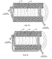
- FIG. 75 is a simplified dual layer Wheeler spiral with similar flowing induced RF currents between layers
- FIG. 76 is an electrical schematic of the structure of FIG. 75 ;
- FIG. 77 is a top down view of the structure of FIG. 75 along lines 77 - 77 ;
- FIG. 78 is a top down view of the structure of FIG. 75 along lines 78 - 78 ;
- FIG. 79 is an expanded isometric view of the structure of FIGS. 77 and 78 ;
- FIG. 80 is an assembled isometric view of the structure of FIG. 79 ;
- FIG. 81 is a manufacturing embodiment of the structures of FIGS. 77 and 78 ;
- FIG. 82 is the next step of the manufacturing embodiment of FIG. 81 ;
- FIG. 83 is a simplified four layer Wheeler spiral with similar flowing induced RF currents between layers
- FIG. 83A is similar to FIG. 83 now showing “n” number of layers
- FIG. 84A is an embodiment of a circuit trace for a Wheeler spiral
- FIG. 84B is another embodiment of a circuit trace for a Wheeler spiral
- FIG. 84C is another embodiment of a circuit trace for a Wheeler spiral
- FIG. 85 is a view similar to the structure of FIG. 80 , now showing a flexible substrate
- FIG. 86 is a view similar to the structure of FIG. 80 , now showing the flexible substrate formed into a roll;
- FIG. 87 is a view similar to the structure of FIG. 80 , now showing a protective or insulative covering
- FIG. 88 is an assembled view of the structure of FIG. 87 ;
- FIG. 89 is a view similar to the structure of FIG. 88 , now showing a flexible substrate
- FIG. 90 is a view similar to the structure of FIG. 88 , now showing the flexible substrate formed into a roll;
- FIG. 91 top view of a high volume manufacturing wafer with multiple bandstop filters of the structure of FIG. 80 .
- the present invention relates to multilayer helical wave filters placed between proximal and distal ends of an implantable lead of an active medical device (AMD).
- AMD active medical device
- One or more multilayer helical wave filters may be implanted anywhere along the length of implanted leads or electrodes of AMDs.
- the multilayer helical wave filter of the present invention presents a very high impedance (which impedes RF current flow) at one or more MRI RF pulsed frequencies.
- the present invention is particularly important to protect implanted leads from overheating in the presence of high power electromagnetic field environments, such as the RF pulsed fields produced by a clinical MRI scanner.
- the present invention comprises a multilayer helical wave filter which is installed in one or more locations along the length of the conductors of an implanted lead. As will be shown, it is also very important that the multilayer helical wave filter be insulated along its entire length with insulation integral to the implanted lead so that RF leakage paths do not occur around the filter through ionic body fluids.
- the multilayer helical wave filter of the present invention acts as an impeding circuit.
- the operation of impeding circuits and diversion circuits is more thoroughly described in U.S. Pat. No. 7,751,903 and US 2010/0160997 A1, which are incorporated herein by reference.
- the multilayer helical wave filter has a Q and 3-dB bandwidth such that, at resonance, it offers attenuation of at least 10-dB over a range of MRI RF pulsed frequencies at least 10 kHz wide, and more preferably at least 100 kHz or even on the order of MHz.
- the novel multilayer helical wave filter of the present invention can be used in combination with any of the diversion circuits as described in U.S. Pat. No. 7,751,903 and US 2010/0160997 A1.
- FIG. 1 is a wire formed diagram of a generic human body showing a number of exemplary implantable medical devices.
- 100 A is a family of implantable hearing devices which can include the group of cochlear implants, piezoelectric sound bridge transducers and the like.
- 100 B includes an entire variety of neurostimulators and brain stimulators.
- 100 C shows a cardiac pacemaker.
- 100 D includes the family of left ventricular assist devices (LVAD's) and artificial hearts.
- LVAD's left ventricular assist devices
- 100 E includes an entire family of drug pumps which can be used for dispensing of insulin, chemotherapy drugs, pain medications and the like.
- 100 F includes a variety of implantable bone growth stimulators for rapid healing of fractures.
- 100 G includes urinary incontinence devices.
- 100 H includes the family of pain relief spinal cord stimulators and anti-tremor stimulators.
- 100 I includes a family of implantable cardioverter defibrillator (ICD) devices, congestive heart failure devices (CHF), and cardio resynchronization therapy devices, otherwise known as CRT devices.
- ICD implantable cardioverter defibrillator
- CHF congestive heart failure devices
- 100 J illustrates a family of probes or catheters that can be transvenously inserted during catheter lab procedures. These are normally considered short-term implants in that they are inserted within the human body for at most a few hours.
- 100 K is an externally worn active medical device, such as a neurostimulator. It can be worn on a belt, placed in a pocket or the like. Typically, it has one or more implanted leads. 100 K also represents an externally worn drug pump or the like.
- AMDs active medical devices
- FIG. 1 generally represent any type of AMD that is either a “long-term” or “short-term” implant.
- “Short-term” implants include AMDs like probes or catheters or surgical devices that are “short-term” body insertions used either for diagnostic or therapy delivery purposes.
- a probe or catheter is typically used in a cath-lab situation wherein it is temporarily inserted through a femoral (or other) artery where the entire procedure lasts minutes or at most a few hours.
- a long-term implant such as a cardiac pacemaker, is generally designed to be implanted in the human body for many years.
- a short-term implant There are significant differences in the art between a short-term and a long-term implant. For example, for a long-term implant, one has to worry greatly about the long-term biocompatibility, toxicity and even the hermeticity of the implant. In contrast, a probe, catheter or temporary loop recorder need only operate or be reliable for a matter of minutes or even hours. In general, a short-term implant is often considered to be a disposable device.
- FDA regulatory approval processes for long-term implants is significantly different and involves much more rigorous testing and product safety and reliability criteria.
- the FDA Center for Devices and Radiological Health (FDA-CDRH) is the responsible regulatory agency for long-term cardiac implants.
- active medical device or active implantable medical device (AIMD) is construed to include long-term implants and also short-term body insertions, such as probes or catheters.
- AMD is inclusive of active implantable medical devices (AIMDs) and also externally worn medical devices that are associated with an implanted lead.
- lead generally refers to implantable leads and their conductors that are external to the housing of the active medical device. These leads tend to have a proximal end, which is at or adjacent to the AMD, and a distal end, which typically includes one or more electrodes which are in contact with body tissue.
- FIG. 2 is a drawing of a typical cardiac pacemaker 100 C showing a titanium case or housing 102 and an IS-1 header connector block 104 .
- the titanium case or housing 102 is hermetically sealed, however there is a point where leadwires 106 a - 106 d must ingress and egress a hermetic seal. This is accomplished by providing a hermetic terminal assembly 108 that generally consists of a ferrule 110 which is laser welded to the titanium housing 102 of the pacemaker 100 C.
- leadwires consisting of leadwire pair 106 a and 106 b and leadwire pair 106 c and 106 d .
- This is typical of what is known as a dual chamber bipolar cardiac pacemaker.
- the IS-1 connectors 112 and 112 ′ of leads 114 and 114 ′ are designed to plug into receptacles 116 and 116 ′ in the header block 104 .
- the receptacles 116 and 116 ′ are low voltage (pacemaker) connectors covered by an ANSI/AAMI ISO standard IS-1. Higher voltage devices, such as implantable cardioverter defibrillators (ICDs), are covered by ANSI/AAMI ISO standard DF-1.
- ICDs implantable cardioverter defibrillators
- a new standard which will integrate both high voltage and low voltage connectors into a miniature in-line quadripolar connector is known as the IS-4 series.
- the implanted leads 114 and 114 ′ are typically routed transvenously in a pacemaker application down into the right atrium 118 and the right ventricle 118 ′ of the heart 120 .
- New generation biventricular or CRT-P devices may introduce leads to the outside of the left ventricle, which devices have proven to be very effective in cardiac resynchronization and treating congestive heart failure (CHF).
- CHF congestive heart failure
- the present invention will be described herein in the context and environment of a cardiac pacemaker 100 C and its associated leads 114 and 114 ′, the present invention may also be advantageously utilized in many other types of AMDs as briefly outlined above and shown in FIG. 1 , as well as in other commercial electronic, military, aerospace and other applications.
- functionally equivalent components will retain the same or a similar reference number, irrespective of the particular embodiment being described.
- FIG. 3 illustrates a prior art single chamber bipolar AMD 100 C and lead system 114 and 114 ′ with a distal tip electrode 122 and a ring electrode 124 typically as used with a cardiac pacemaker 100 C.
- FIG. 4 illustrates a single chamber bipolar cardiac pacemaker 100 C, and leads 114 and 114 ′ having distal tip 122 and distal ring 124 electrodes. This is a spiral wound (coaxial) system where the ring coil 114 ′ is wrapped around the tip coil 114 . There are other types of pacemaker leadwire systems in which these two leads lay parallel to one another (known as a bifilar lead system), which are not shown.
- FIG. 5 is taken from section 5 - 5 of FIG. 4 , and shows multilayer helical wave filters 126 a and 126 b .
- multilayer helical wave filter 126 a of the present invention at or adjacent to the tip electrode 122 also a multilayer helical wave filter 126 b at the ring electrode 124 .
- the multilayer helical wave filters 126 would be tuned to be resonant at a center frequency in a range of MRI RF pulsed frequencies.
- the operation of simple L-C bandstop filters in implanted leads is more thoroughly described by U.S. Pat. No. 7,363,090 and U.S. Pat. No. 7,945,322.
- the performance of the multilayer helical wave filter 126 of the present invention is similar to that of a simple L-C bandstop filter, except that its equivalent circuit diagram is much more complicated.
- the multilayer helical wave filter can be designed with multiple resonances as described herein. It is useful to think of these multiple resonances as equivalent to multiple bandstop filters of varying resonant frequencies that are disposed in series with the implanted lead.
- FIG. 6 illustrates a probe or a catheter 100 J which has four internal conductors 132 a - 132 d which are directed to four different distal electrodes 134 a - 134 d at its distal end.
- electrode 134 d would be known as an ablation electrode wherein the other electrodes could be used for cardiac electrical mapping and the like.
- the probe or catheter 100 J encompasses multilayer helical wave filters 126 a - 126 d of the present invention in series with each of the conductors that are directed to the electrodes 134 a - 134 d .
- the probe or catheter 100 J consists of a flexible and steerable probe or catheter section 136 which may be bent as shown and generally terminates in the distal electrodes 134 a - 134 d .
- FIG. 7 is a sectional view taken generally along section 7 - 7 from FIG. 6 . Shown are the four conductors 132 a - 132 d which are housed inside the probe or catheter steerable body 136 . There are four multilayer helical wave filter 126 a - 126 d in accordance with the present invention. Each of these multilayer helical wave filters 126 is in series with one of the distal electrodes 134 . These multilayer helical wave filters 126 impede MRI RF induced currents from flowing into the electrodes 134 and thereby inadvertently overheating and damaging adjacent living tissues.
- FIG. 8 is an isometric view of a multilayer helical wave filter 126 of the present invention which is in series with an implanted lead (not shown). Also not shown is an overall insulation covering the multilayer helical wave filter which is contiguous with the implanted lead to provide isolation of the multilayer helical wave filter from body fluids. This insulation is omitted for clarity purposes in many of the drawings, however, it will be understood that this insulation is essential so that the impedance of the multilayer helical wave filter at resonance is not degraded by parallel RF current paths through body tissues. Shown is an elongated rectangular conductor 140 with an MRI RF induced current i (t) shown entering it.
- the elongated conductor 140 forms a first helically wound inductor segment 142 .
- a return wire connecting segment 144 (which could be coiled) which is used to wind a second helically wound inductor 146 inside of the first segment.
- the first helically wound inductor segment 142 and the second helically wound inductor segment 146 are wound in the same longitudinal direction and share a common longitudinal axis where planar surfaces of the first helically wound segment 142 face or abut planar surfaces of the second helically wound inductor segment 146 .
- the elongated conductor has a dielectric insulation which may also be used to insulate the entire multilayer helical wave filter such that RF current through body fluids do not degrade its impedance at resonance.
- a capacitance is therefore formed between the planar surfaces of the first helically wound inductor segment 142 and the second helically wound inductor segment 146 .
- FIG. 8 There are a number of advantages to the multilayer helical wave filter construction as illustrated in FIG. 8 .
- FIG. 9 is very similar to FIG. 8 except that the first helically wound segment 142 is much larger in diameter than the second helically wound inductor segment 146 .
- This is to better illustrate the principles of the present invention and also indicate the direction of current flow.
- the RF induced current flow from MRI is always in the same direction. Having the current flow be in the same direction of the various inductor segments of the present invention is critically important and a major distinguishing feature over the prior art.
- the design of the return wire or segment 144 which can be straight, curvilinear or coiled, (and also be either external or internal to the inductor segments) is a key.
- the current flow of adjacent coils is generally in opposite directions (reference Bottomley US 2008/0243218 A1).
- the fields associated with the return wire or segments 144 are negligible in comparison with the fields generated by both the inner and outer multilayer helical inductor segments 142 and 146 .
- the multilayer helical wave filter 126 can be resonant at 1, 2 or even “n” number of selected RF frequencies. Similar effects can be achieved by carefully controlling the overlap area between the planar surfaces of the outer inductor segment 142 and the inner inductor segment 146 . This would affect the amount of parasitic capacitance and hence the resonant frequency.
- the dielectric thickness or the dielectric type can be varied anywhere from two to fifty. Most polymer-type dielectric coatings have a dielectric constant that fall between two and four. However, there are certain other types of dielectrics such as tantalum oxide, which would provide significantly higher dielectric constants (closer to 40). Different materials with different dielectric constants can be used in different sections of the multilayer helical wave filter.
- FIG. 8 one can see that the return wire or segment 144 is directed through the inside of both the first helically wound inductor segment 142 and the second helically wound inductor segment 146 .
- FIG. 9 shows an alternate configuration wherein the return wire or segment 144 returns outside of both the first helically wound inductor segment 142 and the second helically wound inductor segment 146 .
- this return wire or connecting segment 144 is a straight elongated conductor.
- the coiled return path is disposed at an angle to the first and second helically wound segments. This is to reduce the effect of eddy currents due to reverse currents in the return path [ideally close to 90 degrees is better but it could be anywhere greater than 0 degrees except (n*pi) n being 0, 1, 2, etc.].
- This coiled return path is also useful in increasing or controlling the phase shift between the RF induced currents in the first helically wound inductor segment 142 relative to the currents in the second helically wound inductor segment 146 .
- FIG. 10 is taken along section 10 - 10 from FIG. 9 and shows the elongated conductor 140 that forms the first helically wound inductor segment 142 and the second helically wound inductor segment 146 in cross-section.
- a capacitance 148 is formed between each of the coplanar surfaces between the first helically wound inductor 142 and the second helically wound inductor 146 .
- the first helically wound inductor 142 and the second helically wound inductor 146 along with capacitance 148 and 150 form a multilayer helical wave filter in accordance with the present invention.
- capacitance 148 and 150 form a multilayer helical wave filter in accordance with the present invention.
- FIG. 11 illustrates the multilayer helical wave filter previously illustrated in FIGS. 8 and 9 with end caps 152 and 154 for convenient mechanical and electrical connection in series into one or more conductors of an implantable lead of an AIMD.
- an implantable lead 114 may be comprised of material MP35N.
- the lead conductor would be easily laser welded to mandrel end cap 156 of 152 .
- the multilayer helical wave filter of the present invention is disposed between these two end caps.
- End cap 154 is shown connected to a distal electrode in contact with body tissues.
- the multilayer helical wave filter 126 of the present invention can be disposed anywhere along the length of an implanted lead. However, in a particularly preferred embodiment, it is disposed at or near the distal electrode.
- An electrode assembly (not shown) may be electrically and mechanically connected to end cap 154 .
- FIG. 12 is a schematic diagram showing the multilayer helical wave filter 126 disposed between the two end caps 152 and 154 .
- the end caps are shown attached in the implantable lead 114 with one end directed to the AMD and the other end directed to electrode 122 .
- Multiple discrete multilayer helical wave filters may be installed in series anywhere along the length of the implanted lead as well.
- An overall electrical insulation 158 is integral to the lead 114 and also surrounds both end caps 152 and 154 in the entire multilayer helical wave filter 126 . This insulation is very important to prevent RF electrical leakage through body fluids in parallel with the multilayer helical wave filter 126 .
- Such RF leakage currents can significantly degrade the impedance of the multilayer helical wave filter at its one or more resonant frequencies.
- the amount of RF current leakage can be so severe that the multilayer helical wave filter becomes ineffective in preventing a distal electrode from overheating during an MRI scan.
- FIG. 13 is very similar to FIGS. 8, 9 and 10 except that it additionally has a third helically wound inductor segment 160 .
- the structure of FIG. 13 is useful to form multiple resonances to provide a high impedance and therefore a high degree of attenuation to various MRI RF pulsed frequencies. For example, typical 1.5 Tesla scanners operate at an RF pulsed frequency of approximately 64 MHz.
- the implanted lead system can provide a high degree of immunity to overheating from both the 1.5 and 3-Tesla systems. Accordingly, the multilayer helical wave filter can be designed to be resonant at a first, second or even “n” selected RF frequencies.
- FIG. 14 is a sectional view taken from section 14 - 14 from FIG. 13 .
- the three helically wound inductor segments 142 , 146 and 160 are clearly shown.
- the result is a multilayer helical wave filter 126 which could be designed to be resonant at a number of selected MRI RF pulsed frequencies. In general, the resonant frequency of each segment is approximated by the equation:
- f r 1 2 ⁇ ⁇ ⁇ ⁇ LC
- L is the inductance, in Henries, of the inductor component
- C is the capacitance, in Farads, of the capacitor component.
- the resonant frequency, f r is a function of the MRI system of interest. As previously discussed, a 1.5 T MRI system utilizes an RF system operating at approximately 64 MHz, a 3.0 T system utilizes a 128 MHz RF, and so on. By determining the MRI system of interest, only L and C remain. By first selecting one of these two variable parameters, a filter designer needs only to solve for the remaining variable. Note, for a more accurate prediction of resonant frequency f r , the PSPICE circuit of FIG. 23 should be used.
- FIG. 15 is the schematic diagram of the multilayer helical wave filter of FIGS. 13 and 14 illustrating that the wave filter has multiple resonances at fr 1 and fr 2 .
- the multilayer helical wave filter 126 can be designed to be resonant at both 64 MHz (1.5-Tesla MRI) and 128 MHz (3-Tesla MRI). Accordingly, this would provide a very high impedance in the implanted lead during patient exposure to either one of these commonly available MRI scanners.
- FIG. 16 is a graph of attenuation of the multilayer helical wave filter 126 of FIGS. 13 and 14 versus frequency in MHz. As one can see, there is a resonant peak at both fr 1 and fr 2 corresponding to 64 MHz and 128 MHz. In both cases, the impedance of the multilayer helical wave filter 126 is quite high which results in an attenuation value exceeding 10-dB. In general, the attenuation would be measured on a Spectrum Analyzer in a balanced 50-ohm system.
- FIG. 17 is taken generally along section 17 - 17 from FIG. 10 . Shown is the end view of the elongated conductor that forms the first helically wound inductor segment 142 and the second helically wound inductor segment 146 .
- the outer or first helically wound inductor segment 142 is wound very tightly to the second helically wound inductor segment 146 .
- This dielectric coating 162 is very important for two reasons: (1) it prevents adjacent turns from shorting and also prevents the first helically wound inductor segment 142 from shorting to the second helically wound inductor segment 146 ; and (2) the dielectric coating material has a much higher dielectric constant than air, thereby allowing one to increase or tune the capacitances 148 and 150 .
- FIG. 18 is taken generally along section 18 - 18 from FIG. 17 .
- the capacitance 148 is shown.
- the first helically wound inductor 142 would be wound tightly to the second helically wound inductor 146 .
- they are shown separated for convenience so one can show the schematic symbol for the capacitor 148 .
- the amount of parasitic capacitance 148 is determined by the overlap area of the outer helix segment and the inner helix segment.
- One can increase the amount of capacitance by increasing the width of the elongated conductors 142 and 146 .
- the capacitance value is also related to the dielectric constant of the insulating material 162 and also the dielectric thickness of the insulting material 162 . Reducing the dielectric thickness increases the capacitance value significantly. These relationships are expressed ideally by the following equation:
- n the number of overlapping capacitance areas
- k the dielectric constant of the insulating material
- A the effective capacitance area
- t the thickness between opposing plates.
- FIG. 19 is substantially the same as FIG. 17 , except that the conductor is no longer rectangular or square in cross-section.
- the conductor shown in FIG. 19 would be a conventional round wire which would be highly undesirable in the present invention.
- the effective capacitance (ECA) overlap area would be very small. Not only would the resulting capacitance be very small, but it would also be highly variable. As one can see, any slight variations in winding or winding alignment would cause the capacitance value of 148 to vary dramatically. Accordingly, it is a feature of the present invention that the elongated conductor 140 that forms the multilayer helical wave filter 126 be of either rectangular or square wire, preferably coated in a dielectric film 154 or the like.
- the size and shape of the elongated conductor that forms the helically wound segments is important. In general, a square or rectangular cross-section is preferred.
- the designer can control the parasitic capacitance that is formed.
- the designer can control the resonant frequency by controlling both the inductance and the amount of parasitic capacitance that is formed.
- the designer can also control the Q and resulting 3-dB bandwidth at resonance of the multilayer helical wave filter.
- the primary factor in controlling the Q is to control the resistance of the wire that forms the first helical segment and the second helical segment.
- the resistivity of the wire is one of its primary material properties.
- the resistance is also determined by the overall length of the elongated conductor of the first and second helical segments and also inversely related to its cross-sectional area (width times height).
- a primary determining factor of the parasitic capacitance is the effective capacitance area which is determined by the amount of planar surface overlap between the first helically wound segment and the second helically wound segment.
- the first, second and third inductor segments can all be of the same cross-sectional shape and area elongated conductors and of the same number of turns. However, each segment could also have a different cross-sectional area of conductor and even a different number of turns. This affords the designer many degrees of freedom in controlling the inductance, resonant frequency and the Q of each resonant section.
- dielectric coating 154 There are several ways to apply the dielectric coating 154 .
- One way would be to coat the entire elongated conductor wire 140 before forming the first and second helically wound inductor segments 142 and 146 .
- Another way to do this would be through carefully controlled winding processes where the entire assembly was subsequently dipped or subjected to vacuum deposited dielectric material such as parylene.
- a dielectric film could be disposed between the first helically wound inductor segment 142 and the second helically wound inductor segment 146 .
- dielectric insulative materials such as Polyimide, aromatic polyimide, liquid crystal polymer, PTFE, PEEK, ETFE, Parylene, tantalum oxides, any nano-dielectric coating, PFA, FEP, Polyurethane, polyurethane with self-bonding overcoat, polyamide, polyvinyl acetal, polyvinyl acetal overcoated with polyamide, polyurethane overcoated with polyamide, epoxy, polyester (amide) (imide) overcoated with polyamide, polyester (amide) (imide), silicone-treated glass fiber, polyamide-imide, thermoplastic compounds, polyvinylchloride (PVC), polyolefin class: ⁇ LDPE, HDPE, TPO, TPR, polyolefin alloys ⁇ , LDPE low density, HDPE high density, polypropylene (PP), thermoplastic fluoropolymers, TEFLON FEP, Tefzel ETFE, Kynar PVDF, TEFLON PFA, Halar ECTFE,
- FIG. 21 illustrates an alternative construction of the multilayer helical wave filter 126 of the present invention.
- the second helically wound inductor segment 146 is wound inside of the first helically wound inductor segment 142 on the same longitudinal axis.
- the first helically wound inductor segment 142 and the second helically wound inductor segment 146 are wound adjacent to each other side-by-side along the same longitudinal axis.
- FIG. 22 is taken generally along section 22 - 22 from FIG. 21 .
- This shows the elongated conductor 140 of the first helically wound inductor segment 142 alongside the elongated conductor forming the second helically wound inductor segment 146 .
- FIG. 23 is a simplified P-Spice schematic diagram of the multilayer helical wave filter 126 shown in FIGS. 8, 9 and 10 .
- the voltage source shown in FIG. 18 would be the voltage induced in an implanted lead by a medical diagnostic procedure, such as by the RF field of an MRI scanner.
- the load resistance R is shown for simplification and would actually be a complex impedance based on the impedance of the lead system, body tissues and the input impedance of the active medical device (AMD).
- AMD active medical device
- the resistance values R1 and R2 are determined by the classical resistance of any conductor wherein the resistance is proportional to the conductivity Rho (times) the length L (divided by) cross-sectional area A.
- the 3 dB bandwidth of the resonance of the multilayer helical wave filter 126 is determined by its Q at resonance.
- the multilayer helical wave filter 126 can be designed to have multiple resonances at different frequencies. Interestingly, one could also vary either the conductor 140 cross sectional area, material or length in different sections which would result in a different Q and 3-dB bandwidth at each resonant frequency. As one can see, the novel multilayer helical wave filter 126 affords the designer many opportunities to attenuate the current flow of one or multiple RF frequencies.
- FIG. 24 is the frequency response of a 20 turn coaxial 2-layer helical wave filter 126 showing a resonant peak at 144 MHz.
- the cross-sectional area of the elongated conductor that forms the multilayer helical wave filter segments can vary in width anywhere from 0.0005 inches to 0.025 inches.
- the height of the rectangular square wire can also vary anywhere from 0.0005 inches to 0.025 inches. If the elongated conductor is round, the diameter can vary anywhere from 0.0010 to 0.025.
- the multilayer helical wave filter can be particularly designed for cardiac leads, wherein the diameter is typically anywhere from 2 French to 9 French (0.090 inches for 7 French or for neuro leads of 0.052 inches in diameter, which are typically 1 French.
- the multilayer helical wave filter of the present invention can be built in any size from 1 French and above. Shown are the real part, the imaginary part and the absolute values of the impedance.
- Biocompatible materials include MP35N, stainless steel and all of its alloys, tantalum, or drawn filled tubes. Drawn filled tubes can have a core of silver, gold, platinum or the like with an outer coating or tubing of MP35N, stainless steel 316LVN, nitinol or the like. Accordingly, one can control the inductance, the capacitance and the resistance of each segment of the multilayer helical wave filter individually. The resistance will largely determine the Q and the 3-dB bandwidth at each resonance point.
- FIG. 25 shows the helical wave filter 126 of FIG. 8 and FIG. 9 has been modified to show the inductance and the capacitance values 148 and 150 such that the multilayer helical wave filter is resonant at 64 MHz, which corresponds to the RF pulsed frequency for 1.5 Tesla MRI scanners.
- the impedance Z is plotted in kilohms.
- the phase angle is plotted in degrees.
- Markers 1 and 2 shown on the impedance curve correspond with frequencies f 1 and f 2 . These are the 3-dB down points.
- the 3-dB bandwidth is preferably 10 kHz or greater and is the difference in frequency of f 2 ⁇ f 1 .
- the 3-dB bandwidth would be best measured in a Spectrum or Network analyzer in a balanced 50 ohm system measuring attenuation.
- the multilayer helical wave filter 126 of the present invention provides over 1000 ohms (1 kilohm) of impedance at the MRI RF pulsed frequency. This provides a dramatic amount of attenuation and current reduction thereby preventing implanted leads and/or their associated electrodes from overheating during an MR scan.
- Optimal selection of materials and dielectrics can provide up to 5 to 10 kilohms of impedance at resonance.
- FIG. 26 is a Spectrum Analyzer scan taken from an RF probe located inside a 1.5 Tesla clinical MRI scanner.
- the primary RF pulsed frequency is shown as marker 1 as 64 MHz.
- the harmonics of the RF pulsed frequency are generally not specified or controlled by manufacturer specifications or industry standards. In other words, these harmonics are largely uncontrolled.
- the scan shows a harmonic (marker 2) at 128 MHz, a harmonic (marker 3) at 192 MHz, a harmonic (marker 4) at 256 MHz and even a harmonic at 320 MHz (marker 5).
- the primary RF pulsed frequency (64 MHz) and its harmonics can all contribute to RF currents in a lead and particularly RF currents at a distal electrode to tissue interface. Accordingly, the primary frequency and its harmonics can all contribute to leadwire heating.
- the multilayer helical wave filter can be designed to have resonances at the primary MRI RF frequency (64 MHz) and also at some or all of its harmonic frequencies. In general, only harmonics of significant amplitude would require attenuation by the multilayer helical wave filter.
- FIG. 27 is similar to FIG. 8 except that the connecting segment 144 has been coiled around the outside of both the first helically wound inductor 142 and second helically wound inductor 146 segments. Coiling of the return wire 144 decreases its inductance and increases its capacitance. By changing the inductance of the return wire 144 , one controls the phase shift between the RF currents in various segments as previously described. This can be used to introduce a secondary resonance into the multilayer helical wave filter 126 in such a way to provide attenuation at multiple MRI RF pulsed frequencies. For example, attenuation could be provided at both 64 MHz (1.5 Tesla) and 128 MHz (3 Tesla). It will be obvious to one skilled in the art that the multilayer helical wave filter can be designed to have one, two, three or . . . n-resonant frequencies.
- Electrical connections 141 are illustrated to show how one interconnects the return layer to various other layers of the present invention.
- the electrical connection 141 has to be both nontoxic and biocompatible. Suitable electrical connections can be laser welds, gold brazes, other types of brazes, biocompatible thermal-setting conductive adhesives, biocompatible gold-based solders or the like. Importantly, the electrical and mechanical connections 141 could also be done by crimping or other mechanical attachment means.
- FIG. 28 is the side view of the multilayer helical wave filter 126 shown in FIG. 27 .
- FIG. 29 is a sectional view taken generally along line 29 - 29 from FIG. 28 . Shown is the elongated conductor 140 of the first helical wound segment 142 , the second helically wound segment 146 and the connecting segment 144 . A coiled return wire 144 could be applied to any of the previously described multilayer helical wave filters 126 such as shown in FIG. 8, 9, 13 or 21 .
- FIG. 30 illustrates a unipolar pacemaker lead 164 having a proximal connector 166 such as described by International Standards ISO—IS1, DF1, DF4 or IS4.
- This proximal connector 166 would be plugged into a cardiac pacemaker, a cardioverter defibrillator or the like (not shown).
- the distal end of the lead has a tip electrode 122 with tines 168 which are used to grasp trabecular or other tissue within a human heart.
- the lead body has an overall insulation 158 which extends over the multilayer helical wave filter to a point near the distal electrode 122 .
- This insulation is critically important to prevent RF currents from circulating through the body fluids thereby tending to short out or degrade the impedance of the multilayer helical wave filter 126 .
- the overall insulation 158 still provides that the center of the multilayer helical wave filter can be hollow for convenient guide wire insertion.
- the center of the wave filter could incorporate one or more valves such that additional leads or guide wires placed from the proximal side can be routed and sealed. Access from the distal side would be restricted in a similar manner to a hemostasis valve in an introducer.
- the multilayer helical wave filter 126 impedes the undesirable flow of RF currents into body tissues via electrode 122 .
- the lead body has an overall insulation 158 which extends over the multilayer helical wave filter to a point near the distal electrode 122 .
- This insulation is critically important to prevent RF currents from circulating through body fluids thereby tending to short out or degrade the impedance of the multilayer helical wave filter 126 .
- the multilayer helical wave filter 126 prevents overheating of the distal electrode 122 and/or the surrounding body tissues. It has been shown, that overheating of said tissues can cause changes in pacemaker capture threshold or even complete loss of pacing.
- FIG. 31 is a schematic diagram of the unipolar lead 164 of FIG. 30 showing the AMD 100 C and a multilayer helical wave filter 126 of the present invention installed preferably at or near the distal tip electrode 122 .
- FIG. 32 is very similar to FIG. 30 except a bi-polar active fixation electrode 170 is shown at the distal end or tip of the implanted lead.
- the screw-in helix tip electrode 122 has been extended, which would typically be screwed into cardiac tissue.
- a ring electrode 124 forms a bi-polar electrode system wherein pacing and sensing can be conducted between the helix tip electrode 122 and the ring electrode 124 .
- Insulation 158 prevents RF currents from flowing through body fluids and shorting out multilayer helical wave filter 126 a and insulation material 158 ′ insulates multilayer helical wave filter 126 b and performs the same function.
- the insulating layer 158 also protects the implanted lead, provides flexibility and lubricity and aids in the long-term reliability of the overall lead system.
- FIG. 33 is the schematic diagram of the bi-polar lead previously illustrated in FIG. 32 .
- the active implantable medical device such as a cardiac pacemaker 100 C with implanted lead conductors 114 and 114 ′.
- Lead conductor 114 is directed in series with a multilayer helical wave filter of the present invention to ring electrode 124 .
- Lead conductor 114 ′ has multilayer helical wave filter 126 a in series with tip electrode 122 .
- the multilayer helical wave filter 126 a and 126 b are very near or at the respective distal electrodes. This prevents RF current induction from MRI fields from coupling around the wave filters and inducing currents in the distal electrodes.
- FIG. 35 is a sectional view of the three electrode configurations illustrated in FIG. 34 .
- the filter region consists of three multilayer helical wave filters of the present invention. That, in turn, is connected to the implanted lead.
- Electrodes 122 a , 122 b and 122 c are typically the ring or pad electrodes of a neural lead.
- FIG. 36 is the schematic diagram of the three electrode multilayer helical wave filter of FIG. 35 . Shown are three multilayer helical wave filter segments 126 a , 126 b and 126 c shown in series with each of the three ring or paddles electrodes 122 a , 122 b and 122 c . Each of the conductors of the implanted lead 114 a , 114 b and 114 c are shown connected to the active implantable medical device 100 C.
- FIG. 37 illustrates an 8-pin paddle electrode 172 commonly used in spinal cord stimulator applications.
- the eight paddle electrodes are shown as 176 a through 176 h.
- FIG. 38 is the reverse side of the paddle electrode 172 of FIG. 37 .
- FIG. 39 is a cross-section taken generally from section 39 - 39 from FIG. 37 .
- electrodes shall include any type of electrode in contact with body tissue. This includes, but is not limited to, pacemaker electrodes, endocardial electrodes, epicardial electrodes, defibrillator shocking coils, tip electrodes, ring electrodes, ablation electrodes, deep brain electrodes, nerve cuff electrodes, various types of paddle electrodes, cochlear electrode bundles, Bions, probe and catheter electrodes and the like.
- FIG. 40 is a special multilayer helical wave filter with three return conductors 144 a , 144 b and 144 c which form two discrete multilayer helical wave filters 126 a and 126 b that are in series with each other.
- each one would have a selected RF resonant frequency.
- the first resonant frequency f r1 would be the RF pulsed frequency of a 1.5-Tesla common MRI scanner at 64 MHz.
- the second multilayer helical wave filter portion would be resonant f rz at 128 MHz which is the RF pulsed frequency for commonly available 3-Tesla MR scanners.
- the resonant frequencies f r1 and f r2 can be precisely tuned.
- FIG. 41 is a schematic diagram of the multilayer helical wave filter of FIG. 40 showing that it provides (in one package) for two resonances in series which are shown as f r1 and f r2 .
- FIG. 42 illustrates that any number of individual or separate discrete multilayer helical wave filters 126 can be placed in series in any conductor of any implanted lead in multiple locations along the lead length.
- three different helical wave filters could be placed in series along the length of an implanted lead as shown.
- FIG. 42 there are three different helical wave filters that are resonant at f r1 , f r2 and f r3 .
- any number of helical wave filters can be placed in series in an implanted lead.
- multiple resonances fr 1 and fr 2 . . . or fr n can be created by multiple segments in a single multilayer helical wave filter or multiple resonances can also be achieved by installing a multiplicity of discrete wave filters along the length of the lead as shown in FIG. 42 .
- FIG. 43 illustrates the multilayer helical wave filter 126 with end caps 152 and 154 that were previously illustrated in FIG. 11 .
- End cap 152 is shown attached to the conductor 114 of an implanted lead 158 which has an overall insulation sheath 158 .
- the multilayer helical wave filter 126 presents 2000 ohms at its primary resonant frequency of 64 MHz.
- the 2000 ohms of impedance desirably impedes the flow of MRI induced RF currents into body tissue through the electrode 122 .
- FIG. 44 is the schematic diagram taken from FIG. 43 showing the 2000-ohm impedance Z F of the multilayer helical wave filter 126 . Shown in parallel with the multilayer helical wave filter 126 is the leakage path or 80-ohm impedance of the body tissues Z L . Using the parallel resistance formula, when one has 80 ohms in parallel with 2000 ohms, the result is a combined impedance Z TOT of 76.82 ohms. As one can see, this is a catastrophic reduction of the impedance of the multilayer helical wave filter at resonance. It is a critical feature of the present invention that these body fluid paths be insulated so that they cannot cause leakage in parallel with the multilayer helical wave filter of the present invention.
- FIG. 45 is very similar to FIG. 43 except that the lead insulation 158 ′ has been extended completely over the multilayer helical wave filter 126 of the present invention. Accordingly, the leakage paths through ionic body fluid L 1 and L 2 have been eliminated. In this case, the multilayer helical wave filter of FIG. 45 would present the full 2000 ohms of impedance at the MRI RF-pulsed frequency.
- FIG. 46 illustrates an active fixation helix tip electrode assembly typically used in cardiac pacemaker applications. Shown is a multilayer helical wave filter 126 of the present invention. In this case, the multilayer helical wave filter is shown in a hermetic subassembly 180 . Electrically isolating electric components in a medical electric lead with an active fixation electrode are described in US 2010/0324240 (see FIG. 10 ) the contents of which are incorporated herein.
- FIG. 46 illustrates an exemplary bipolar active fixation electrode 170 which embodies a lead body 178 , a coaxial conductor 114 ′ for the ring electrode 124 and coaxial conductor 114 for the tip (active fixation helix) electrode 122 , a collar 180 , and the translatable casing 182 which houses a multilayer helical wave filter 126 of the present invention.
- the translatable casing 182 includes a pins 152 and 154 .
- the pin 152 is electrically and mechanically connected to the tip electrode lead wire conductor 114 and the pin 154 is attached to the translatable seal assembly 184 which is also connected to a distal helix electrode 122 .
- the distal helix electrode 122 is also known as an active fixation electrode.
- the pin 152 , the casing 182 , the pin 154 and the translatable seal structure 184 all form what is defined herein as a casing subassembly 186 .
- a casing 182 which houses the multilayer helical wave filter 126 can be a hermetic seal as previously described in FIG. 10 or US 2010/0324640 or it can be a rigid or semi-rigid subassembly similar to that previously illustrated in FIG. 11 herein.
- these parallel ionic conduction paths can seriously degrade the impedance of the wave filter at resonance.
- a laser weld (not shown) electrically and mechanically connecting the tip conductor 114 to pin 152 .
- a laser weld 188 connecting pin 154 to a weld sleeve 190 of the translatable seal assembly 184 .
- the weld sleeve 190 may be attached to the pin 154 in any known technique including laser welding, bonding, crimping, adhering, brazing, other forms of welding, or any other suitable method.
- the weld sleeve 190 is typically laser welded to the helix electrode 122 .
- the active fixation helix tip electrode 122 is retracted (as shown) so that it will not inadvertently stab or poke into body tissues during lead insertion.
- the physician takes a special tool and twists the proximal end of lead body 178 tip conductor 114 which causes the entire conductor 114 and casing subassembly 182 to rotate.
- the distal helix electrode 122 rotates, it engages a guide 192 which causes the helix 122 to extend and screw into body tissue.
- the guide 192 may be formed as part of the collar 180 and engages the tip electrode 122 when the tip conductor 114 is rotated.
- the rotation causes the helical tip electrode 122 to rotate within the collar 180 and thereby translate in a forward manner.
- the tip electrode 122 is advancing relative to the collar 180 , it is engaging with body tissue by being screwed directly into the tissue forming an attachment.
- the tip electrode 122 can be rotated in the opposite direction by the tip conductor 114 and thereby disengaged from the tissue for removal and/or reattachment at a different location. This is a method of active affixation which is well known in the art.
- the flexible seal 194 of FIG. 46 slides against the interior of the collar 180 thereby preventing the entrance of ionic body fluids into the inside of the lead body 178 .
- the seal 194 may be bonded, molded, adhered, or formed onto the weld sleeve 190 by any suitable means.
- the seal 194 can be formed in a multitude of ways appreciated by those skilled in the art, such as multiple wipers, o-rings, thin disks or sheets, and various molded profiles.
- the optional O-ring seal 196 is disposed between the inside diameter of the lead collar 180 and the outside diameter of the translatable housing and multilayer helical wave filter 126 .
- the purpose of seal 194 and the O-ring seal 196 is to ensure that ionic body fluids cannot be disposed across the important electrical path between pins 152 and 154 . Ionic body fluids can represent an undesirable parallel path as low as 80 ohms. Over time, due to bulk permeability, body fluids will penetrate into the interior of the lead body 178 . However, this is an osmotic type of action.
- the resulting fluids that would occur over long periods of time inside the lead body 178 would be distilled and free of ionic contaminants (de-ionized). This means that they would be less conductive of high frequency electrical signals from one end to the other of the multilayer helical wave filter 182 , 126 .
- the presence of optional O-ring 196 is desirable in that it also presents a high impedance to such a parallel circuit path.
- the casing 182 , 126 may also have a conformal insulative coating (not shown) for further electrically isolating terminals 152 and 154 such that a parallel path through body fluid is further impeded.
- the insulative coating may be formed from any suitable material, such as a dielectric material, including, but not limited to parylene, ETFE, PTFE, polyamide, polyurethane and silicone. It will be understood that the exemplary embodiment of FIG. 46 may work with or without such coatings.
- the casing 182 may be a metallic and hermetically container or any biocompatible insulative material.
- the multilayer helical waver filter of the present invention is hollow on the inside for convenient insertion of additional wires.
- the multilayer helical wave or bandstop filters 126 of the present invention resonate at one or more frequencies and thereby provide a very high impedance at a selected resonant frequency(ies) or range of frequencies, and comprises an elongated conductor 140 having at least one planar surface.
- the elongated conductor includes a first helically wound segment 142 having a first end and a second end forming a first inductor component, a return wire or return coil 144 , and a second helically wound segment 146 having a first end and a second end forming a second inductor component.
- the first and second helically wound segments share a common longitudinal axis and are wound in the same direction wherein induced currents also flow in the same direction.
- the return wire or return coil 144 extends substantially to the length of the first and second helically wound inductor segments to connect the second end of the first helically wound segment to the first end of the second helically wound segment.
- the planar surface or surfaces of the first inductor faces the planar surface or surfaces of the second inductor and are coated with a dielectric insulative layer.
- Parasitic capacitance is formed between the planar surfaces of both the inner and outer inductors and adjacent coils.
- the combination of the inductors and the parasitic capacitances form a multi-helical wave filter, which in preferred embodiments act as a bandstop filter.
- FIG. 47 is a multihelical wave filter 126 which is very similar to the multihelical wave filter previously illustrated in FIG. 27 .
- the coiled return wire 144 is wound in the opposite direction. Winding the return coil in the opposite direction changes the overlapping magnetic fields and also the parasitic capacitance.
- FIG. 47 is a more efficient structure in that it will yield a higher impedance at resonance as compared to the structure illustrated in FIG. 27 .
- FIG. 48 is very similar to FIG. 28 except that again, the coiled return wire 144 is wound in the opposite direction.
- the inner coil 146 and the outer coil 142 are wound in opposite directions as compared to FIG. 47 .
- the return wire 144 is also wound in the opposite direction. In other words, as long as one is consistent, the coils can all be wound as shown in FIG. 47 or in the reverse configuration as shown in FIG. 48 .
- FIG. 49 is a sectional view taken from section 49 - 49 from FIG. 48 illustrating a first helically wound segment 146 , a second helically wound segment 142 and the return wire segment 144 .
- This is a rectangular conductor as shown or a round or other shape (not shown) can be used in a continuous winding wherein, the inner coil is formed in one direction and then the return coil is formed in the other direction. Then the outer coil is formed as illustrated. In this way, the coil is wrapped back and forth, again to facilitate ease of construction.
- FIG. 24 The graph of the resonant frequency is shown typically in FIG. 24 .
- a prototype wound in accordance with FIG. 27 has a resonant frequency of approximately 152 MHz.
- the resonant frequency of the structure illustrated in FIG. 47 shifted to just below 116 MHz.
- capacitor 148 represents the parasitic capacitance of the return wires as it overlaps the inner windings. In FIG. 47 , this value of capacitance is significantly different as compared to winding the return wire in the opposite direction, as shown in FIG. 27 .
- FIG. 50 illustrates the same structure as previously described in FIG. 47 except that the return wire coils 144 are more closely spaced and there are more of them.
- the coil spacing of the return wire 144 can vary anywhere from widely spaced, to tightly aligned such that the return wire coils would be wound adjacent similar to those shown in outer coil 142 .
- FIG. 51 is very similar to FIG. 48 illustrating the same principle wherein, the number of return wire coils 144 per inch can be increased.
- FIG. 52 is a sectional view taken from section 52 - 52 from FIG. 51 .
- the return coils 144 are more closely spaced as compared to return wire coils 144 previously illustrated in FIG. 49 .
- FIG. 53 is very similar to FIG. 52 except that the return wire coil 144 is shown very closely spaced. In other words, there are a much greater number of return wire coils as compared to FIG. 52 or 49 .
- the inner coil 146 and the outer coil 142 are of a D-shaped wire such that the wire forms a semi-circle. These wires are, of course, insulated (not shown) so that a dielectric layer is formed between them. This allows for a relatively high parasitic capacitance C P to form between these two layers which is best illustrated in the blown up view shown in FIG. 54 taken from section 54 - 54 from FIG. 53 . Referring once again to FIG. 54 , one can see that there is a flat surface 212 between conductors 142 and 146 . This makes for a highly controllable effective capacitance area (ECA) and maximizes the parasitic capacitances as opposed to say two round wires.
- ECA effective capacitance area
- FIG. 55 illustrates a multi-section and multilayer helical bandstop filter which has a continuous inner coil 146 . There is also an outer coil 142 which is discontinuous and unique to the two sections fr1 and fr2. Referring once again to FIG. 55 , one can see that in the fr1 section, there is a much higher turn count n1 compared to the relatively lower turn count n2 of the fr2 section. Referring once again to FIG. 55 and FIG. 56 , one can see that there are two different return coil segments 144 and 144 ′, which yields two discrete bandstop filters with a common inner core 146 .
- the schematic diagram in FIG. 57 illustrates two simplified bandstop filters consisting of an inductor L in parallel with a capacitor C.
- section fr1 there is a different inductance of capacitance L1 and a different value of total parasitic capacitance C1 as compared to the resonant section fr2, which has a different value of equivalent value L2 and a different value of parasitic capacitance C2.
- the schematic diagram in FIG. 57 is simplified and does not show all of the individual parasitic capacitances between adjacent layers and between adjacent turns.
- FIGS. 58 and 59 are very similar to FIGS. 55 and 56 except that there is an inner coil 146 and 146 ′, which is discontinuous and then a continuous outer coil 142 , which is continuous throughout and two different return segments 144 and 144 ′.
- FIGS. 58 and 59 where 142 is continuous whereas, in FIGS. 55 and 56 where 146 is continuous.
- Manufacturing of multilayer helical inductors for human implant applications is a challenging one because of the need for complete biocompatibility. This means that all of the material must be nontoxic and long term compatible with body fluid. In addition, they must not erode over time such that electrical connections would be degraded.
- FIG. 60 illustrates an embodiment of the present invention that is applicable to any of the previous drawings of multihelical bandstop filters.
- FIG. 61 is a sectional view taken from section 61 - 61 from FIG. 60 showing the interior structure of the multihelical bandstop filter 126 and the end cap structures 200 and 200 ′.
- crimp areas 202 , 202 ′, 202 ′′ and 202 ′′′ make all of the required electrical connections for any of the multilayer helical bandstop filters of the present invention.
- An advantage to crimping is that a very solid mechanical and electrical connection is made without the need for laser welding or the like.
- One of the problems associated with laser welding is that it tends to burn the electrical insulation or dielectric material which coats all of the wires of the present invention.
- bandstop filter 126 By stripping away this electrical insulation and then crimping it between two biocompatible metal structures, such as platinum, one makes a highly reliable biocompatible nontoxic stable electrical connection.
- the three layers of coiled wire that form that bandstop filter 126 incorporate round wire.
- this round wire would have to be insulated such that adjacent turns don't short out to each other.
- the insulation between coil layers and turns also creates a parasitic capacitance which yields resonant bandstop filter performance.
- the wires could be cored. It is well known in the prior art that defibrillator leads have a solid silver center surrounded by an MP35N biocompatible outer coating. The presence of the silver greatly increases the conductivity of the wire.
- the crimping type connections shown in FIG. 1 are particularly advantageous such that, the integrity of the core of the wire is preserved and the core would not be exposed to body fluids.
- round wires have been used to create the bandstop filter portion 126 . It will be obvious to those skilled in the art that any of the previously described wire, such as rectangular or D-shaped and the like could also be used.
- FIG. 62 illustrates another method of efficiently manufacturing a multilayer helical inductor of the present invention.
- one uses a double insulated wound wire 204 similar to speaker wires typically found in a stereo store.
- the doubled wire 204 has been split into a portion that will be connected and aligned with the lead conductor and after it's split and separated, its other half 208 will be routed to a return route or a return segment.
- a return wire (not shown) would be either routed straight or coiled in either direction between ends 208 and 208 ′.
- the first step is to route the double wire on a mandrel. In FIG.
- the second step is to separate the ends of each wire.
- a return wrap or coil 210 is wound outside of both the inner wires 204 .
- This return wire 210 acts as a single wire.
- the return wire 210 would be electrically connected to return wrap 208 (not shown) and on the right hand side (as illustrated in FIG. 65 ), the return wrap 210 would be electrically connected to the split end of the dual wire 208 ′.
- FIG. 66 is a sectional view taken from section 66 - 66 from FIG. 65 showing the double inner wire 204 and the single return wire wrap 210 .
- FIGS. 67 through 72 show alternative wire shapes along with their associated electrical insulation 214 .
- round wires, D-shaped wires, rectangular wires, square wires or even oval or electrical wires could be used in the present invention.
- FIGS. 67 through 72 one can see there are two layers of insulation 214 and 216 . In this case, all of the different wire shapes are individually insulated and then there is an over mold or insulation 214 to provide addition insulation, but more importantly, to hold them mechanically and structurally together into the shapes as illustrated.
- FIGS. 73 and 74 are similar to FIG. 66 except that additional layers of double wires are used.
- FIG. 73 there are two layers of doubled wires 204 and 204 ′.
- FIG. 74 there are three layers 204 , 204 ′ and 204 ′′.
- FIG. 75 illustrates a dual layer square Wheeler spiral multihelical inductor bandstop filter of the present invention.
- a contact or circuit trace pad 300 which is electrically conductive and is connectable to an implanted lead which has a distal electrode in contact with biological cells.
- the implantable lead when exposed to an MRI environment, can pick up high amplitude RF pulse signals, which are routed as a circuit current i.
- Contact pad 302 ′ is routed to a circuit trace 312 , which forms a second square Wheeler spiral inductor in stacked relationship with the first Wheeler spiral terminating at contact pad 302 ′′. It will be obvious to those skilled in the art that the Wheeler spiral could be round, oval, rectangular, irregular or the like.
- Contact pad 302 ′′ is also connected to a via hole with via hole conductive fill material 310 , which makes contact to the upper via hole pad area 302 ′′′.
- Contact pad 302 ′′′ is also connected to a circuit trace 312 ′ as shown.
- the RF currents are routed upwards from contact pad 302 ′′ to contact pad 302 ′′′ and then the currents are routed along the circuit trace 312 ′ where they exit the Wheeler spiral and terminate at contact pad 300 ′.
- Contact pad 300 ′ has an electrical connection 306 where the circuit trace 312 is terminated.
- FIG. 75 it is an essential feature of the present invention that the induced RF currents in the upper circuit trace layer 312 ′ are in the same direction as the RF circuit currents induced in the lower circuit trace 312 .
- a bandstop filter when one has a capacitor in parallel with an inductor, one has a bandstop filter, which can be designed to be resonant at an MRI RF-pulsed frequency.
- a bandstop filter When a bandstop filter is resonant, it provides a very high impedance at the resonant frequency, thereby preventing the flow of RF currents.
- the structure as illustrated in FIG. 75 would be a bandstop filter placed at, near or within a distal electrode. By presenting a high impedance at RF frequencies, one would prevent dangerous RF currents from entering into adjacent body tissues, thereby causing direct damage or overheating of adjacent structures.
- FIG. 77 is a top down view of the upper layer taken along section 77 - 77 from FIG. 75 .
- the via hole connection pads 302 and 302 ′′′ are shown.
- FIG. 78 is a top down view of the lower layer taken generally along section 78 - 78 from FIG. 75 .
- the circuit trace 312 and contact pads 302 ′ and 302 ′′ As previously mentioned, this is a square Wheeler spiral. It is also possible as a round Wheeler spiral or any other shape. It is apparent that FIGS. 77 and 78 show an increased number of turns as compared to FIG. 75 .
- FIG. 79 is an isometric view of the multilayer Wheeler spiral helical bandstop filter taken from FIGS. 75, 77 and 78 .
- the thickness 308 In this case, it is exploded so one can see all the internal circuitry.
- the thickness between adjacent layers 308 is also greatly exploded so one can see the Wheeler spiral shapes of the upper and lower sections.
- FIG. 80 is more realistic of the actual dielectric thickness 308 ′ wherein, the Wheeler spirals have been deposited on the very thin dielectric layers which are laminated into a single structure.
- the contact pads 300 at 300 ′ and that the Wheeler spiral circuit trace structures are actually an overlay of circuit traces 312 and 312 ′.
- the circuit traces 312 and the contact pads 302 and the electrical interconnections would all be of suitable biocompatible materials.
- the insulative or dielectric layer 308 ′ separating them would also be of suitable biocompatible materials. This would allow one to construct bandstop filters for use in the electrodes of various types of active implantable medical devices, such as neurostimulator arrays and the like.
- biocompatible circuit traces 312 would include biocompatible metals, such as MP35N, gold, platinum and the like.
- FIG. 81 illustrates a method of manufacturing where the upper and lower layers of the Wheeler spiral multihelical wave filter 301 of FIG. 79 .
- the upper and lower layers, including circuit traces 312 ′ and 312 are all screened on a single dielectric or polymer carrier or film 314 .
- FIG. 82 becomes the multihelical Wheeler spiral structure 301 previously described in FIG. 80 .
- FIG. 83 is very similar to FIG. 75 except in this case, there are four layers ( 312 , 312 ′, 312 ′′, 312 ′′′) of novel Wheeler spirals that have been constructed such that the RF-induced currents are always in the same direction in each layer. As previously described, this leads for optimal magnetic coupling and optimal parasitic capacitance such to maximize the impedance of the bandstop filter at resonance. It will be obvious to those skilled in the art that any number of layers, including “n” number of layers, could be used for the novel Wheeler spiral bandstop filters 301 of the present invention as shown in FIG. 83A .
- FIGS. 84A through 84C represent alternate versions of the top layer of the Wheeler spiral bandstop filters 301 of the present invention illustrating a circular shape as shown in FIG. 84A , a rectangular shape as shown in FIG. 84B , or even a hexagon as shown in FIG. 84C .
- FIGS. 84A through 84C just the upper layer of what would be a multilayer Wheeler spiral bandstop filter is illustrated in FIGS. 84A through 84C . It would be obvious to those skilled in the art that any number of layers of the same shapes could be laid up as previously described in FIG. 75 or in FIG. 83 .
- FIG. 85 illustrates the extreme flexibility of the multilayer Wheeler spiral bandstop filter 301 of the present invention.
- These thin films are highly flexible and can even be rolled into a cylindrical shape as shown in FIG. 86 .
- a cylindrical shape is a much better form factor for venous insertion, or even tunneling, as opposed to a flat square or rectangular shape.
- the Wheeler spiral bandstop filter could be rolled around a mandrel or core of the lead such to facilitate the passage of the guide wire to facilitate transvenous insertion and steering.
- the Wheeler spiral bandstop filter may be constructed from a tape-based flexible base as the tape can have its own attachment or other material material suitable for forming these structures.
- Wheeler spiral bandstop filter By spin coating onto a flexible substrate.
- Wheeler spiral bandstop filter patterns may also be created using conventional sputter or evaporation techniques, and from patterning such as using photoresist, etching and then photoresist removal processes.
- biocompatible dielectric materials or thin films include nonconductive polyimide, silicone and the like.
- the examples of the dielectric substrate having bioinert/biocompatible polymers include polydimethylsoloxanes (PDMS), polyethyleneterephthalate (PET), teflons, teflons doped with dielectrics or other, polytetrafluoroethylene (PTFE), ethylenetetrafluoroethylene (ETFE), parylenes, polyether block amide (PEBAX), polyetheretherketone (PEEK), polystyrenes, polysulfones, polypropylenes, polycarbonates, polyvinyl chloride (PVC), polyxylylene polymers, polyamides, polyimides, nylon, epoxies, and other such suitable polymers, elastomers and gels, including combinations thereof.
- PDMS polydimethylsoloxanes
- PET polyethyleneterephthalate
- teflons teflons doped with dielectrics or other
- PTFE polytetrafluoroethylene
- ETFE ethylenetetra
- the examples of the dielectric substrate having configurable materials include photosensitive polymers and co-polymers, elastomers and gels, such as but not limited to photosensitive or photopatternable polymers, microstructured dielectric rubbers, biocompatible dielectric particles (micron, submicron, nano and ultranano) embedded in flexible, stretchable, conformal biocompatible substrates such as but not limited to silicones, urethanes, PDMS, PET, and composites of combinations thereof either as a unique, single material structure or configurable into layered structures wherein the layers may be made with and without filler materials, all of the above including combinations thereof.
- photosensitive polymers and co-polymers, elastomers and gels such as but not limited to photosensitive or photopatternable polymers, microstructured dielectric rubbers, biocompatible dielectric particles (micron, submicron, nano and ultranano) embedded in flexible, stretchable, conformal biocompatible substrates such as but not limited to silicones, urethanes, PDMS, PET, and
- the examples of the dielectric substrate having carbon materials include pyrolitic and vitreous carbons, composites using nano and ultranano carbons, fiber, chopped fiber, ground chopped fiber, submicron fibers, whiskers and the like, nanocrystalline (NCD) and ultrananocrystalline diamond (UNCD), intrinsic diamond, doped diamond, hybrid biocompatible oxide/NCD layered combinations, hybrid biocompatible oxide/UNCD layered combinations, including combinations thereof.
- the examples of the dielectric substrate having other materials include talcs, minerals (such as calcium carbonate, titanium dioxide, aluminum dioxide, sapphire, mica, silica), vapor deposited, e-beam deposited oxide, and atomic layer deposited films such as tantalum oxide (Ta2O5), anodized tantalum, aluminum oxide (Al2O3), titanium oxide (TiO2), anodized titanium, tantalum nitride (TaN), titanium nitride (TiN), silicon nitride (SiN), barium titanate (BaTiO3), silicon oxide (SiO2), hafnium oxide (HfO2) and the like, including combinations thereof.
- talcs minerals
- minerals such as calcium carbonate, titanium dioxide, aluminum dioxide, sapphire, mica, silica
- vapor deposited, e-beam deposited oxide and atomic layer deposited films
- tantalum oxide (Ta2O5) anodized tantalum, aluminum oxide (
- FIG. 87 represents the Wheeler spiral wave filter 301 from FIG. 80 wherein, an upper insulating sheet 318 and a lower insulating sheet 318 ′ have been placed over the top and bottom. This is desirable in that it provides electrical insulation and mechanical protection to the circuit trace layers 312 and 312 ′.
- the contact pads 300 and 300 ′ are exposed to facilitate suitable electrical connection. Alternatively, even after electrical connections have been made to the contact pads 300 , the insulation material 318 , 318 ′ could be added and then could at that time, after the electrical connections are formed be also overlaid over the contact pads 300 and 300 ′ (not shown).
- FIG. 89 and FIG. 90 illustrate that the insulative structure of FIG. 88 with insulation layers 318 , 318 ′ can still all be formed of flexible materials such that they can be bent or rolled up as shown in FIG. 90 .
- FIG. 91 is a top view of a high volume manufacturing wafer indicating that many bandstop filter layers can be silk-screened, sputtered or electrically deposited as a thin-film at one time. After construction, they can be diced out of the carrier or the bar in a high volume, highly efficient operation.
Abstract
Description
Where fr is the resonant frequency, L is the inductance, in Henries, of the inductor component, and C is the capacitance, in Farads, of the capacitor component. In this equation, there are three variables: fr, L, and C. The resonant frequency, fr, is a function of the MRI system of interest. As previously discussed, a 1.5 T MRI system utilizes an RF system operating at approximately 64 MHz, a 3.0 T system utilizes a 128 MHz RF, and so on. By determining the MRI system of interest, only L and C remain. By first selecting one of these two variable parameters, a filter designer needs only to solve for the remaining variable. Note, for a more accurate prediction of resonant frequency fr, the PSPICE circuit of
where n is the number of overlapping capacitance areas, k is the dielectric constant of the insulating material, A is the effective capacitance area and t is the thickness between opposing plates. For the overlapping faces of the inner and outer segments of a multilayer helical wave filter, the effective capacitance area is relatively large since it includes the entire overlap area. This gives the designer many degrees of freedom in selecting the primary
Claims (31)
Priority Applications (3)
| Application Number | Priority Date | Filing Date | Title |
|---|---|---|---|
| US13/958,604 US9468750B2 (en) | 2006-11-09 | 2013-08-04 | Multilayer planar spiral inductor filter for medical therapeutic or diagnostic applications |
| EP14172182.9A EP2835148A1 (en) | 2013-08-04 | 2014-06-12 | Multilayer planar spiral inductor filter for medical, therapeutic or diagnostic applications |
| EP17178510.8A EP3269419A1 (en) | 2013-08-04 | 2014-06-12 | Multilayer planar spiral inductor filter for medical, therapeutic or diagnostic applications |
Applications Claiming Priority (8)
| Application Number | Priority Date | Filing Date | Title |
|---|---|---|---|
| US11/558,349 US7945322B2 (en) | 2005-11-11 | 2006-11-09 | Tank filters placed in series with the lead wires or circuits of active medical devices to enhance MRI compatibility |
| US36982210P | 2010-08-02 | 2010-08-02 | |
| US12/873,862 US8224440B2 (en) | 2006-11-09 | 2010-09-01 | Electrically isolating electrical components in a medical electrical lead with an active fixation electrode |
| US12/938,774 US8463375B2 (en) | 2005-11-11 | 2010-11-03 | Tank filters placed in series with the lead wires or circuits of active medical devices to enhance MRI compatability |
| US13/081,314 US8649857B2 (en) | 2006-06-08 | 2011-04-06 | Tank filters placed in series with the lead wires or circuits of active medical devices to enhance MRI compatibility |
| US13/193,501 US8239041B2 (en) | 2010-08-02 | 2011-07-28 | Multilayer helical wave filter for medical therapeutic or diagnostic applications |
| US13/562,169 US9254377B2 (en) | 2010-08-02 | 2012-07-30 | Multilayer helical wave filter for medical therapeutic or diagnostic applications |
| US13/958,604 US9468750B2 (en) | 2006-11-09 | 2013-08-04 | Multilayer planar spiral inductor filter for medical therapeutic or diagnostic applications |
Related Parent Applications (1)
| Application Number | Title | Priority Date | Filing Date |
|---|---|---|---|
| US13/562,169 Continuation-In-Part US9254377B2 (en) | 2006-11-09 | 2012-07-30 | Multilayer helical wave filter for medical therapeutic or diagnostic applications |
Publications (2)
| Publication Number | Publication Date |
|---|---|
| US20130338747A1 US20130338747A1 (en) | 2013-12-19 |
| US9468750B2 true US9468750B2 (en) | 2016-10-18 |
Family
ID=49756599
Family Applications (1)
| Application Number | Title | Priority Date | Filing Date |
|---|---|---|---|
| US13/958,604 Expired - Fee Related US9468750B2 (en) | 2006-11-09 | 2013-08-04 | Multilayer planar spiral inductor filter for medical therapeutic or diagnostic applications |
Country Status (1)
| Country | Link |
|---|---|
| US (1) | US9468750B2 (en) |
Families Citing this family (6)
| Publication number | Priority date | Publication date | Assignee | Title |
|---|---|---|---|---|
| EP3009165A1 (en) | 2014-10-16 | 2016-04-20 | BIOTRONIK SE & Co. KG | Implantable electrical lead |
| EP3025756B1 (en) * | 2014-11-27 | 2019-01-09 | BIOTRONIK SE & Co. KG | Electrode extension integrated in an active implant |
| US10183162B2 (en) * | 2015-01-02 | 2019-01-22 | Greatbatch Ltd. | Coiled, closed-loop RF current attenuator configured to be placed about an implantable lead conductor |
| EP3206061A1 (en) * | 2016-02-15 | 2017-08-16 | Leica Instruments (Singapore) Pte. Ltd. | Illumination filter system and observation system for a multispectral fluorescence microscope |
| SG10201912373QA (en) * | 2016-12-02 | 2020-02-27 | Carver Scientific Inc | Memory device and capacitive energy storage device |
| EP4349397A1 (en) * | 2022-10-07 | 2024-04-10 | Greatbatch Ltd. | High-voltage electrical insulation for use in active implantable medical devices circuit board connectors |
Citations (114)
| Publication number | Priority date | Publication date | Assignee | Title |
|---|---|---|---|---|
| US3871382A (en) | 1973-02-15 | 1975-03-18 | Pacesetter Syst | Heart stimulator system for rapid implantation and removal with improved integrity |
| US3968802A (en) | 1975-01-24 | 1976-07-13 | Medtronic, Inc. | Cautery protection circuit for a heart pacemaker |
| US3980975A (en) | 1975-09-08 | 1976-09-14 | Varian Associates | Broadband microwave bias network |
| US4236127A (en) | 1977-04-13 | 1980-11-25 | Pyrohm, Inc. | Electrical frequency responsive structure |
| JPS60141034U (en) | 1984-02-29 | 1985-09-18 | カシオ計算機株式会社 | keyboard |
| JPS61181925U (en) | 1985-05-07 | 1986-11-13 | ||
| US4633181A (en) | 1983-08-11 | 1986-12-30 | Regents Of The University Of Calif. | Apparatus and method for increasing the sensitivity of a nuclear magnetic resonance probe |
| US4654880A (en) | 1983-12-09 | 1987-03-31 | Minnesota Mining And Manufacturing Company | Signal transmission system |
| US4689621A (en) | 1986-03-31 | 1987-08-25 | The United States Of America As Represented By The Administrator Of The National Aeronautics And Space Administration | Temperature responsive transmitter |
| US4799499A (en) | 1985-08-17 | 1989-01-24 | Bisping Hans Juergen | Implantable electrode with active fixation means |
| US4858623A (en) | 1987-07-13 | 1989-08-22 | Intermedics, Inc. | Active fixation mechanism for lead assembly of an implantable cardiac stimulator |
| EP0145430B1 (en) | 1983-12-09 | 1991-05-29 | Cochlear Corporation | Signal transmission system |
| US5082888A (en) * | 1988-10-07 | 1992-01-21 | Mitsui Toatsu Chemicals, Inc. | Polypropylene resin composition having high dielectric strength |
| US5209233A (en) | 1985-08-09 | 1993-05-11 | Picker International, Inc. | Temperature sensing and control system for cardiac monitoring electrodes |
| US5217010A (en) | 1991-05-28 | 1993-06-08 | The Johns Hopkins University | Ecg amplifier and cardiac pacemaker for use during magnetic resonance imaging |
| US5246438A (en) | 1988-11-25 | 1993-09-21 | Sensor Electronics, Inc. | Method of radiofrequency ablation |
| US5291180A (en) * | 1981-10-30 | 1994-03-01 | Reeb Max E | LC structure useful in radio frequency security systems |
| US5300108A (en) | 1993-01-05 | 1994-04-05 | Telectronics Pacing Systems, Inc. | Active fixation lead with a dual-pitch, free spinning compound screw |
| US5333095A (en) | 1993-05-03 | 1994-07-26 | Maxwell Laboratories, Inc., Sierra Capacitor Filter Division | Feedthrough filter capacitor assembly for human implant |
| US5363845A (en) | 1993-08-13 | 1994-11-15 | Medical Advances, Inc. | Breast coil for magnetic resonance imaging |
| US5398683A (en) | 1991-05-24 | 1995-03-21 | Ep Technologies, Inc. | Combination monophasic action potential/ablation catheter and high-performance filter system |
| US5428337A (en) | 1992-02-21 | 1995-06-27 | Vlt Corporation | Conductive winding |
| US5545201A (en) | 1995-03-29 | 1996-08-13 | Pacesetter, Inc. | Bipolar active fixation lead for sensing and pacing the heart |
| US5629622A (en) | 1995-07-11 | 1997-05-13 | Hewlett-Packard Company | Magnetic field sense system for the protection of connected electronic devices |
| US5697958A (en) | 1995-06-07 | 1997-12-16 | Intermedics, Inc. | Electromagnetic noise detector for implantable medical devices |
| US5716390A (en) | 1996-08-09 | 1998-02-10 | Pacesetter, Inc. | Reduced diameter active fixation pacing lead using concentric interleaved coils |
| US5722998A (en) | 1995-06-07 | 1998-03-03 | Intermedics, Inc. | Apparatus and method for the control of an implantable medical device |
| US5741321A (en) | 1996-01-11 | 1998-04-21 | Medtronic, Inc. | Active fixation medical electrical lead having improved turning tool |
| US5751539A (en) | 1996-04-30 | 1998-05-12 | Maxwell Laboratories, Inc. | EMI filter for human implantable heart defibrillators and pacemakers |
| US5759202A (en) | 1997-04-28 | 1998-06-02 | Sulzer Intermedics Inc. | Endocardial lead with lateral active fixation |
| US5874745A (en) * | 1997-08-05 | 1999-02-23 | International Business Machines Corporation | Thin film transistor with carbonaceous gate dielectric |
| WO1999019739A1 (en) | 1997-10-13 | 1999-04-22 | Andreas Melzer | Mr imaging method and medical device for use in method |
| US5905627A (en) | 1997-09-10 | 1999-05-18 | Maxwell Energy Products, Inc. | Internally grounded feedthrough filter capacitor |
| JPH11239572A (en) | 1997-12-16 | 1999-09-07 | Koninkl Philips Electronics Nv | Mr system, medical treatment system and localization method |
| US5959829A (en) | 1998-02-18 | 1999-09-28 | Maxwell Energy Products, Inc. | Chip capacitor electromagnetic interference filter |
| US5964705A (en) | 1997-08-22 | 1999-10-12 | Image-Guided Drug Delivery System, Inc. | MR-compatible medical devices |
| US5973906A (en) | 1998-03-17 | 1999-10-26 | Maxwell Energy Products, Inc. | Chip capacitors and chip capacitor electromagnetic interference filters |
| US5978204A (en) | 1995-11-27 | 1999-11-02 | Maxwell Energy Products, Inc. | Capacitor with dual element electrode plates |
| US6008980A (en) | 1997-11-13 | 1999-12-28 | Maxwell Energy Products, Inc. | Hermetically sealed EMI feedthrough filter capacitor for human implant and other applications |
| US6055457A (en) | 1998-03-13 | 2000-04-25 | Medtronic, Inc. | Single pass A-V lead with active fixation device |
| US6101417A (en) | 1998-05-12 | 2000-08-08 | Pacesetter, Inc. | Implantable electrical device incorporating a magnetoresistive magnetic field sensor |
| US6141594A (en) | 1998-07-22 | 2000-10-31 | Cardiac Pacemakers, Inc. | Single pass lead and system with active and passive fixation elements |
| US6159560A (en) | 1998-11-25 | 2000-12-12 | Stevenson; Robert A. | Process for depositing a metal coating on a metallic component of an electrical structure |
| US6275369B1 (en) | 1997-11-13 | 2001-08-14 | Robert A. Stevenson | EMI filter feedthough terminal assembly having a capture flange to facilitate automated assembly |
| US6424234B1 (en) | 1998-09-18 | 2002-07-23 | Greatbatch-Sierra, Inc. | Electromagnetic interference (emi) filter and process for providing electromagnetic compatibility of an electronic device while in the presence of an electromagnetic emitter operating at the same frequency |
| US6456481B1 (en) | 2001-05-31 | 2002-09-24 | Greatbatch-Sierra, Inc. | Integrated EMI filter-DC blocking capacitor |
| WO2002083016A1 (en) | 2001-04-13 | 2002-10-24 | Surgi-Vision, Inc. | Systems and methods for magnetic-resonance-guided interventional procedures |
| US6473291B1 (en) | 1999-03-16 | 2002-10-29 | Gb Aquisition Co., Inc. | Low inductance four terminal capacitor lead frame |
| US6493591B1 (en) | 2000-07-19 | 2002-12-10 | Medtronic, Inc. | Implantable active fixation lead with guidewire tip |
| US20030028094A1 (en) | 1996-04-25 | 2003-02-06 | Ananda Kumar | Biopsy and sampling needle antennas for magnetic resonance imaging-guided biopsies |
| US6529103B1 (en) | 2000-09-07 | 2003-03-04 | Greatbatch-Sierra, Inc. | Internally grounded feedthrough filter capacitor with improved ground plane design for human implant and other applications |
| US20030050557A1 (en) | 1998-11-04 | 2003-03-13 | Susil Robert C. | Systems and methods for magnetic-resonance-guided interventional procedures |
| US6535766B1 (en) | 2000-08-26 | 2003-03-18 | Medtronic, Inc. | Implanted medical device telemetry using integrated microelectromechanical filtering |
| US6539253B2 (en) | 2000-08-26 | 2003-03-25 | Medtronic, Inc. | Implantable medical device incorporating integrated circuit notch filters |
| US6567703B1 (en) | 2000-11-08 | 2003-05-20 | Medtronic, Inc. | Implantable medical device incorporating miniaturized circuit module |
| US6567259B2 (en) | 2001-05-31 | 2003-05-20 | Greatbatch-Sierra, Inc. | Monolithic ceramic capacitor with barium titinate dielectric curie point optimized for active implantable medical devices operating at 37° C. |
| US20030144720A1 (en) | 2002-01-29 | 2003-07-31 | Villaseca Eduardo H. | Electromagnetic trap for a lead |
| US6606513B2 (en) | 2000-02-01 | 2003-08-12 | Surgi-Vision, Inc. | Magnetic resonance imaging transseptal needle antenna |
| US6643903B2 (en) | 1997-11-13 | 2003-11-11 | Greatbatch-Sierra, Inc. | Process for manufacturing an EMI filter feedthrough terminal assembly |
| US6675033B1 (en) | 1999-04-15 | 2004-01-06 | Johns Hopkins University School Of Medicine | Magnetic resonance imaging guidewire probe |
| US6675779B2 (en) | 2002-06-13 | 2004-01-13 | Stant Manufacturing Inc. | Dual float valve for fuel tank vent with liquid carryover filter |
| US6687550B1 (en) | 2001-06-01 | 2004-02-03 | Pacesetter, Inc. | Active fixation electrode lead having an electrical coupling mechanism |
| US6701176B1 (en) | 1998-11-04 | 2004-03-02 | Johns Hopkins University School Of Medicine | Magnetic-resonance-guided imaging, electrophysiology, and ablation |
| US6765780B2 (en) | 2002-02-28 | 2004-07-20 | Greatbatch-Sierra, Inc. | EMI feedthrough filter terminal assembly having surface mounted, internally grounded hybrid capacitor |
| US20040263174A1 (en) | 2003-06-24 | 2004-12-30 | Biophan Technologies, Inc. | Magnetic resonance imaging interference immune device |
| US6868288B2 (en) | 2000-08-26 | 2005-03-15 | Medtronic, Inc. | Implanted medical device telemetry using integrated thin film bulk acoustic resonator filtering |
| US6876885B2 (en) | 2001-01-31 | 2005-04-05 | Medtronic, Inc. | Implantable bifurcated gastrointestinal lead with active fixation |
| US20050077984A1 (en) | 2003-10-08 | 2005-04-14 | Lee Byoung Hwa | Laminated low pass filter |
| US6882248B2 (en) | 2000-09-07 | 2005-04-19 | Greatbatch-Sierra, Inc. | EMI filtered connectors using internally grounded feedthrough capacitors |
| US6898454B2 (en) | 1996-04-25 | 2005-05-24 | The Johns Hopkins University | Systems and methods for evaluating the urethra and the periurethral tissues |
| US6925328B2 (en) | 2000-04-20 | 2005-08-02 | Biophan Technologies, Inc. | MRI-compatible implantable device |
| US6931286B2 (en) | 2002-10-02 | 2005-08-16 | Medtronic, Inc. | Delivery of active fixation implatable lead systems |
| US20050197677A1 (en) | 2004-02-12 | 2005-09-08 | Stevenson Robert A. | Apparatus and process for reducing the susceptability of active implantable medical devices to medical procedures such as magnetic resonance imaging |
| US6952613B2 (en) | 2001-01-31 | 2005-10-04 | Medtronic, Inc. | Implantable gastrointestinal lead with active fixation |
| US6971391B1 (en) | 2002-12-18 | 2005-12-06 | Nanoset, Llc | Protective assembly |
| US6985347B2 (en) | 2002-02-28 | 2006-01-10 | Greatbatch-Sierra, Inc. | EMI filter capacitors designed for direct body fluid exposure |
| US20060009819A1 (en) | 2004-07-12 | 2006-01-12 | Medtronic, Inc. | Medical electrical device including novel means for reducing high frequency electromagnetic field-induced tissue heating |
| US6999818B2 (en) | 2003-05-23 | 2006-02-14 | Greatbatch-Sierra, Inc. | Inductor capacitor EMI filter for human implant applications |
| US20060041294A1 (en) | 2004-08-20 | 2006-02-23 | Biophan Technologies, Inc. | Magnetic resonance imaging interference immune device |
| US7038900B2 (en) | 2003-02-27 | 2006-05-02 | Greatbatch-Sierra, Inc. | EMI filter terminal assembly with wire bond pads for human implant applications |
| US7092766B1 (en) | 2003-11-19 | 2006-08-15 | Pacesetter, Inc. | Active fixation lead with multiple density |
| US7148783B2 (en) | 2004-11-05 | 2006-12-12 | Harris Corporation | Microwave tunable inductor and associated methods |
| US20080049376A1 (en) | 1998-11-04 | 2008-02-28 | Greatbatch Ltd. | Non-ferromagnetic tank filters in lead wires of active implantable medical devices to enhance mri compatibility |
| US20080051854A1 (en) | 2005-11-04 | 2008-02-28 | Cherik Bulkes | Mri compatible implanted electronic medical device with power and data communication capability |
| JP4071536B2 (en) | 2002-05-07 | 2008-04-02 | 富士通株式会社 | Test apparatus for file apparatus and test method in test apparatus for file apparatus |
| US7363090B2 (en) | 2001-04-13 | 2008-04-22 | Greatbatch Ltd. | Band stop filter employing a capacitor and an inductor tank circuit to enhance MRI compatibility of active implantable medical devices |
| US20080243218A1 (en) | 2007-03-19 | 2008-10-02 | Bottomley Paul A | Mri and rf compatible leads and related methods of operating and fabricating leads |
| US20080262584A1 (en) * | 2007-03-19 | 2008-10-23 | Bottomley Paul A | Methods and apparatus for fabricating leads with conductors and related flexible lead configurations |
| US7511921B2 (en) | 2003-12-04 | 2009-03-31 | Seagate Technology Llc | Read and write heads with at least a portion of the coil positioned about the write pole opposite the read transducer to reduce adjacent track erasure |
| WO2009045102A2 (en) * | 2007-10-02 | 2009-04-09 | Polymer Vision Limited | An electronic circuit element with profiled photopatternable dielectric layer |
| US7561906B2 (en) | 2005-05-04 | 2009-07-14 | Boston Scientific Neuromodulation Corporation | Electrical lead for an electronic device such as an implantable device |
| US20090179716A1 (en) | 2008-01-09 | 2009-07-16 | Anaren, Inc. | RF Filter Device |
| US20090281592A1 (en) | 2008-05-08 | 2009-11-12 | Pacesetter, Inc. | Shaft-mounted rf filtering elements for implantable medical device lead to reduce lead heating during mri |
| US20100010602A1 (en) | 2006-11-30 | 2010-01-14 | Wedan Steven R | Rf rejecting lead |
| US20100076538A1 (en) | 2008-09-22 | 2010-03-25 | Cardiac Pacemakers, Inc. | Styrene-isobutylene copolymers and medical devices containing the same |
| US7702387B2 (en) | 2006-06-08 | 2010-04-20 | Greatbatch Ltd. | Tank filters adaptable for placement with a guide wire, in series with the lead wires or circuits of active medical devices to enhance MRI compatibility |
| US20100114277A1 (en) | 2008-10-30 | 2010-05-06 | Pacesetter, Inc. | Mri compatible implantable medical lead and method of making same |
| US20100160997A1 (en) | 2001-04-13 | 2010-06-24 | Greatbatch Ltd. | Tuned energy balanced system for minimizing heating and/or to provide emi protection of implanted leads in a high power electromagnetic field environment |
| US7751903B2 (en) | 2002-04-15 | 2010-07-06 | Greatbatch Ltd. | Frequency selective passive component networks for implantable leads of active implantable medical devices utilizing an energy dissipating surface |
| US20100174349A1 (en) | 2001-04-13 | 2010-07-08 | Greatbatch Ltd. | System for terminating abandoned implanted leads to minimize heating in high power electromagnetic field environments |
| US20100174348A1 (en) | 2009-01-05 | 2010-07-08 | Cherik Bulkes | Mri compatible electrical lead for an implanted electronic medical device |
| US20100217262A1 (en) | 2001-04-13 | 2010-08-26 | Greatbatch Ltd. | Frequency selective passive component networks for active implantable medical devices utilizing an energy dissipating surface |
| US7853324B2 (en) | 2005-11-11 | 2010-12-14 | Greatbatch Ltd. | Tank filters utilizing very low K materials, in series with lead wires or circuits of active medical devices to enhance MRI compatibility |
| US7853325B2 (en) | 2001-04-13 | 2010-12-14 | Greatbatch Ltd. | Cylindrical bandstop filters for medical lead systems |
| US20100318164A1 (en) | 2009-06-15 | 2010-12-16 | Pacesetter, Inc. | Mri compatible implantable lead with a distributed band stop filter |
| US20110004283A1 (en) | 2008-03-20 | 2011-01-06 | Greatbatch Ltd. | Shielded three-terminal flat-through emi/energy dissipating filter |
| US20110015713A1 (en) | 2008-10-23 | 2011-01-20 | Pacesetter, Inc. | Systems and methods for reducing lead heating and the risks of mri-induced stimulation |
| US7899551B2 (en) | 2001-04-13 | 2011-03-01 | Greatbatch Ltd. | Medical lead system utilizing electromagnetic bandstop filters |
| US7917213B2 (en) | 2005-11-04 | 2011-03-29 | Kenergy, Inc. | MRI compatible implanted electronic medical lead |
| US7945322B2 (en) | 2005-11-11 | 2011-05-17 | Greatbatch Ltd. | Tank filters placed in series with the lead wires or circuits of active medical devices to enhance MRI compatibility |
| US20110144734A1 (en) | 2001-04-13 | 2011-06-16 | Greatbatch Ltd. | Medical lead system utilizing electromagnetic bandstop filters |
| US20110196462A1 (en) | 2010-02-11 | 2011-08-11 | Ingo Weiss | Electrode device for active medical implant |
| US20110230943A1 (en) | 2010-03-17 | 2011-09-22 | Greatbatch Ltd. | Implantable lead for an active medical device having an inductor design minimizing eddy current losses |
| US20120029342A1 (en) | 2010-08-02 | 2012-02-02 | Greatbatch Ltd. | Multilayer helical wave filter for medical therapeutic or diagnostic applications |
-
2013
- 2013-08-04 US US13/958,604 patent/US9468750B2/en not_active Expired - Fee Related
Patent Citations (132)
| Publication number | Priority date | Publication date | Assignee | Title |
|---|---|---|---|---|
| US3871382A (en) | 1973-02-15 | 1975-03-18 | Pacesetter Syst | Heart stimulator system for rapid implantation and removal with improved integrity |
| US3968802A (en) | 1975-01-24 | 1976-07-13 | Medtronic, Inc. | Cautery protection circuit for a heart pacemaker |
| US3980975A (en) | 1975-09-08 | 1976-09-14 | Varian Associates | Broadband microwave bias network |
| US4236127A (en) | 1977-04-13 | 1980-11-25 | Pyrohm, Inc. | Electrical frequency responsive structure |
| US5291180A (en) * | 1981-10-30 | 1994-03-01 | Reeb Max E | LC structure useful in radio frequency security systems |
| US4633181A (en) | 1983-08-11 | 1986-12-30 | Regents Of The University Of Calif. | Apparatus and method for increasing the sensitivity of a nuclear magnetic resonance probe |
| EP0145430B1 (en) | 1983-12-09 | 1991-05-29 | Cochlear Corporation | Signal transmission system |
| US4654880A (en) | 1983-12-09 | 1987-03-31 | Minnesota Mining And Manufacturing Company | Signal transmission system |
| JPS60141034U (en) | 1984-02-29 | 1985-09-18 | カシオ計算機株式会社 | keyboard |
| JPS61181925U (en) | 1985-05-07 | 1986-11-13 | ||
| US5209233A (en) | 1985-08-09 | 1993-05-11 | Picker International, Inc. | Temperature sensing and control system for cardiac monitoring electrodes |
| US4799499A (en) | 1985-08-17 | 1989-01-24 | Bisping Hans Juergen | Implantable electrode with active fixation means |
| US4689621A (en) | 1986-03-31 | 1987-08-25 | The United States Of America As Represented By The Administrator Of The National Aeronautics And Space Administration | Temperature responsive transmitter |
| EP0243573A2 (en) | 1986-03-31 | 1987-11-04 | National Aeronautics And Space Administration | Temperature responsive transmitter |
| JPS62233905A (en) | 1986-03-31 | 1987-10-14 | ナシヨナル・エアロノ−テイツクス・アンド・スペ−ス・アドミニストレ−シヨン | Temperature sensitive transmitter |
| US4858623A (en) | 1987-07-13 | 1989-08-22 | Intermedics, Inc. | Active fixation mechanism for lead assembly of an implantable cardiac stimulator |
| US5082888A (en) * | 1988-10-07 | 1992-01-21 | Mitsui Toatsu Chemicals, Inc. | Polypropylene resin composition having high dielectric strength |
| US5246438A (en) | 1988-11-25 | 1993-09-21 | Sensor Electronics, Inc. | Method of radiofrequency ablation |
| EP0498996B1 (en) | 1991-02-11 | 1997-03-05 | Picker International, Inc. | Apparatus and methods for non-invasive examination |
| US5398683A (en) | 1991-05-24 | 1995-03-21 | Ep Technologies, Inc. | Combination monophasic action potential/ablation catheter and high-performance filter system |
| US5217010A (en) | 1991-05-28 | 1993-06-08 | The Johns Hopkins University | Ecg amplifier and cardiac pacemaker for use during magnetic resonance imaging |
| US5428337A (en) | 1992-02-21 | 1995-06-27 | Vlt Corporation | Conductive winding |
| US5300108A (en) | 1993-01-05 | 1994-04-05 | Telectronics Pacing Systems, Inc. | Active fixation lead with a dual-pitch, free spinning compound screw |
| US5514173A (en) | 1993-01-05 | 1996-05-07 | Rebell; Allan K. | Active fixation lead with a dual-pitch, free spinning compound screw |
| US5333095A (en) | 1993-05-03 | 1994-07-26 | Maxwell Laboratories, Inc., Sierra Capacitor Filter Division | Feedthrough filter capacitor assembly for human implant |
| US5363845A (en) | 1993-08-13 | 1994-11-15 | Medical Advances, Inc. | Breast coil for magnetic resonance imaging |
| US5545201A (en) | 1995-03-29 | 1996-08-13 | Pacesetter, Inc. | Bipolar active fixation lead for sensing and pacing the heart |
| US5722998A (en) | 1995-06-07 | 1998-03-03 | Intermedics, Inc. | Apparatus and method for the control of an implantable medical device |
| US5697958A (en) | 1995-06-07 | 1997-12-16 | Intermedics, Inc. | Electromagnetic noise detector for implantable medical devices |
| US5629622A (en) | 1995-07-11 | 1997-05-13 | Hewlett-Packard Company | Magnetic field sense system for the protection of connected electronic devices |
| US5978204A (en) | 1995-11-27 | 1999-11-02 | Maxwell Energy Products, Inc. | Capacitor with dual element electrode plates |
| US5741321A (en) | 1996-01-11 | 1998-04-21 | Medtronic, Inc. | Active fixation medical electrical lead having improved turning tool |
| US6898454B2 (en) | 1996-04-25 | 2005-05-24 | The Johns Hopkins University | Systems and methods for evaluating the urethra and the periurethral tissues |
| US20030028094A1 (en) | 1996-04-25 | 2003-02-06 | Ananda Kumar | Biopsy and sampling needle antennas for magnetic resonance imaging-guided biopsies |
| US5751539A (en) | 1996-04-30 | 1998-05-12 | Maxwell Laboratories, Inc. | EMI filter for human implantable heart defibrillators and pacemakers |
| US5716390A (en) | 1996-08-09 | 1998-02-10 | Pacesetter, Inc. | Reduced diameter active fixation pacing lead using concentric interleaved coils |
| US5759202A (en) | 1997-04-28 | 1998-06-02 | Sulzer Intermedics Inc. | Endocardial lead with lateral active fixation |
| US5874745A (en) * | 1997-08-05 | 1999-02-23 | International Business Machines Corporation | Thin film transistor with carbonaceous gate dielectric |
| US5964705A (en) | 1997-08-22 | 1999-10-12 | Image-Guided Drug Delivery System, Inc. | MR-compatible medical devices |
| US5905627A (en) | 1997-09-10 | 1999-05-18 | Maxwell Energy Products, Inc. | Internally grounded feedthrough filter capacitor |
| EP1021730B1 (en) | 1997-10-13 | 2003-04-02 | Simag GmbH | MR imaging system and vena cava filter therefor |
| US6847837B1 (en) | 1997-10-13 | 2005-01-25 | Simag Gmbh | MR imaging method and medical device for use in method |
| WO1999019739A1 (en) | 1997-10-13 | 1999-04-22 | Andreas Melzer | Mr imaging method and medical device for use in method |
| US6280385B1 (en) | 1997-10-13 | 2001-08-28 | Simag Gmbh | Stent and MR imaging process for the imaging and the determination of the position of a stent |
| US6008980A (en) | 1997-11-13 | 1999-12-28 | Maxwell Energy Products, Inc. | Hermetically sealed EMI feedthrough filter capacitor for human implant and other applications |
| US6275369B1 (en) | 1997-11-13 | 2001-08-14 | Robert A. Stevenson | EMI filter feedthough terminal assembly having a capture flange to facilitate automated assembly |
| US6643903B2 (en) | 1997-11-13 | 2003-11-11 | Greatbatch-Sierra, Inc. | Process for manufacturing an EMI filter feedthrough terminal assembly |
| US6236205B1 (en) | 1997-12-16 | 2001-05-22 | U.S. Philips Corporation | MR device provided with a medical instrument, and method of determining the position of the medical instrument |
| EP0930509B1 (en) | 1997-12-16 | 2004-03-17 | Philips Intellectual Property & Standards GmbH | MR device comprising a medical instrument and method for determining the location of the medical instrument |
| JPH11239572A (en) | 1997-12-16 | 1999-09-07 | Koninkl Philips Electronics Nv | Mr system, medical treatment system and localization method |
| US5959829A (en) | 1998-02-18 | 1999-09-28 | Maxwell Energy Products, Inc. | Chip capacitor electromagnetic interference filter |
| US6055457A (en) | 1998-03-13 | 2000-04-25 | Medtronic, Inc. | Single pass A-V lead with active fixation device |
| US5973906A (en) | 1998-03-17 | 1999-10-26 | Maxwell Energy Products, Inc. | Chip capacitors and chip capacitor electromagnetic interference filters |
| US6101417A (en) | 1998-05-12 | 2000-08-08 | Pacesetter, Inc. | Implantable electrical device incorporating a magnetoresistive magnetic field sensor |
| US6141594A (en) | 1998-07-22 | 2000-10-31 | Cardiac Pacemakers, Inc. | Single pass lead and system with active and passive fixation elements |
| US6424234B1 (en) | 1998-09-18 | 2002-07-23 | Greatbatch-Sierra, Inc. | Electromagnetic interference (emi) filter and process for providing electromagnetic compatibility of an electronic device while in the presence of an electromagnetic emitter operating at the same frequency |
| US20080049376A1 (en) | 1998-11-04 | 2008-02-28 | Greatbatch Ltd. | Non-ferromagnetic tank filters in lead wires of active implantable medical devices to enhance mri compatibility |
| US20030050557A1 (en) | 1998-11-04 | 2003-03-13 | Susil Robert C. | Systems and methods for magnetic-resonance-guided interventional procedures |
| US20040167392A1 (en) | 1998-11-04 | 2004-08-26 | Halperin Henry R. | Brain therapy |
| US6701176B1 (en) | 1998-11-04 | 2004-03-02 | Johns Hopkins University School Of Medicine | Magnetic-resonance-guided imaging, electrophysiology, and ablation |
| US7155271B2 (en) | 1998-11-04 | 2006-12-26 | Johns Hopkins University School Of Medicine | System and method for magnetic-resonance-guided electrophysiologic and ablation procedures |
| US20060100506A1 (en) | 1998-11-04 | 2006-05-11 | Johns Hopkins University School Of Medicine | System and method for magnetic-resonance-guided electrophysiologic and ablation procedures |
| US6159560A (en) | 1998-11-25 | 2000-12-12 | Stevenson; Robert A. | Process for depositing a metal coating on a metallic component of an electrical structure |
| US6473291B1 (en) | 1999-03-16 | 2002-10-29 | Gb Aquisition Co., Inc. | Low inductance four terminal capacitor lead frame |
| US6675033B1 (en) | 1999-04-15 | 2004-01-06 | Johns Hopkins University School Of Medicine | Magnetic resonance imaging guidewire probe |
| US6606513B2 (en) | 2000-02-01 | 2003-08-12 | Surgi-Vision, Inc. | Magnetic resonance imaging transseptal needle antenna |
| US6925328B2 (en) | 2000-04-20 | 2005-08-02 | Biophan Technologies, Inc. | MRI-compatible implantable device |
| US6493591B1 (en) | 2000-07-19 | 2002-12-10 | Medtronic, Inc. | Implantable active fixation lead with guidewire tip |
| US6539253B2 (en) | 2000-08-26 | 2003-03-25 | Medtronic, Inc. | Implantable medical device incorporating integrated circuit notch filters |
| US6535766B1 (en) | 2000-08-26 | 2003-03-18 | Medtronic, Inc. | Implanted medical device telemetry using integrated microelectromechanical filtering |
| US6868288B2 (en) | 2000-08-26 | 2005-03-15 | Medtronic, Inc. | Implanted medical device telemetry using integrated thin film bulk acoustic resonator filtering |
| US6566978B2 (en) | 2000-09-07 | 2003-05-20 | Greatbatch-Sierra, Inc. | Feedthrough capacitor filter assemblies with leak detection vents |
| US6529103B1 (en) | 2000-09-07 | 2003-03-04 | Greatbatch-Sierra, Inc. | Internally grounded feedthrough filter capacitor with improved ground plane design for human implant and other applications |
| US6882248B2 (en) | 2000-09-07 | 2005-04-19 | Greatbatch-Sierra, Inc. | EMI filtered connectors using internally grounded feedthrough capacitors |
| US6567703B1 (en) | 2000-11-08 | 2003-05-20 | Medtronic, Inc. | Implantable medical device incorporating miniaturized circuit module |
| US6876885B2 (en) | 2001-01-31 | 2005-04-05 | Medtronic, Inc. | Implantable bifurcated gastrointestinal lead with active fixation |
| US6952613B2 (en) | 2001-01-31 | 2005-10-04 | Medtronic, Inc. | Implantable gastrointestinal lead with active fixation |
| US20110144734A1 (en) | 2001-04-13 | 2011-06-16 | Greatbatch Ltd. | Medical lead system utilizing electromagnetic bandstop filters |
| US20100174349A1 (en) | 2001-04-13 | 2010-07-08 | Greatbatch Ltd. | System for terminating abandoned implanted leads to minimize heating in high power electromagnetic field environments |
| WO2002083016A1 (en) | 2001-04-13 | 2002-10-24 | Surgi-Vision, Inc. | Systems and methods for magnetic-resonance-guided interventional procedures |
| US20100160997A1 (en) | 2001-04-13 | 2010-06-24 | Greatbatch Ltd. | Tuned energy balanced system for minimizing heating and/or to provide emi protection of implanted leads in a high power electromagnetic field environment |
| US20100217262A1 (en) | 2001-04-13 | 2010-08-26 | Greatbatch Ltd. | Frequency selective passive component networks for active implantable medical devices utilizing an energy dissipating surface |
| US7363090B2 (en) | 2001-04-13 | 2008-04-22 | Greatbatch Ltd. | Band stop filter employing a capacitor and an inductor tank circuit to enhance MRI compatibility of active implantable medical devices |
| US7853325B2 (en) | 2001-04-13 | 2010-12-14 | Greatbatch Ltd. | Cylindrical bandstop filters for medical lead systems |
| US7899551B2 (en) | 2001-04-13 | 2011-03-01 | Greatbatch Ltd. | Medical lead system utilizing electromagnetic bandstop filters |
| US6456481B1 (en) | 2001-05-31 | 2002-09-24 | Greatbatch-Sierra, Inc. | Integrated EMI filter-DC blocking capacitor |
| US6567259B2 (en) | 2001-05-31 | 2003-05-20 | Greatbatch-Sierra, Inc. | Monolithic ceramic capacitor with barium titinate dielectric curie point optimized for active implantable medical devices operating at 37° C. |
| US6687550B1 (en) | 2001-06-01 | 2004-02-03 | Pacesetter, Inc. | Active fixation electrode lead having an electrical coupling mechanism |
| US7013180B2 (en) | 2002-01-29 | 2006-03-14 | Medtronic, Inc. | Conditioning of coupled electromagnetic signals on a lead |
| US20030144720A1 (en) | 2002-01-29 | 2003-07-31 | Villaseca Eduardo H. | Electromagnetic trap for a lead |
| US6985347B2 (en) | 2002-02-28 | 2006-01-10 | Greatbatch-Sierra, Inc. | EMI filter capacitors designed for direct body fluid exposure |
| US7113387B2 (en) | 2002-02-28 | 2006-09-26 | Greatbatch-Sierra, Inc. | EMI filter capacitors designed for direct body fluid exposure |
| US6765780B2 (en) | 2002-02-28 | 2004-07-20 | Greatbatch-Sierra, Inc. | EMI feedthrough filter terminal assembly having surface mounted, internally grounded hybrid capacitor |
| US7751903B2 (en) | 2002-04-15 | 2010-07-06 | Greatbatch Ltd. | Frequency selective passive component networks for implantable leads of active implantable medical devices utilizing an energy dissipating surface |
| JP4071536B2 (en) | 2002-05-07 | 2008-04-02 | 富士通株式会社 | Test apparatus for file apparatus and test method in test apparatus for file apparatus |
| US6675779B2 (en) | 2002-06-13 | 2004-01-13 | Stant Manufacturing Inc. | Dual float valve for fuel tank vent with liquid carryover filter |
| US6931286B2 (en) | 2002-10-02 | 2005-08-16 | Medtronic, Inc. | Delivery of active fixation implatable lead systems |
| US6971391B1 (en) | 2002-12-18 | 2005-12-06 | Nanoset, Llc | Protective assembly |
| US7038900B2 (en) | 2003-02-27 | 2006-05-02 | Greatbatch-Sierra, Inc. | EMI filter terminal assembly with wire bond pads for human implant applications |
| US6999818B2 (en) | 2003-05-23 | 2006-02-14 | Greatbatch-Sierra, Inc. | Inductor capacitor EMI filter for human implant applications |
| US20040263174A1 (en) | 2003-06-24 | 2004-12-30 | Biophan Technologies, Inc. | Magnetic resonance imaging interference immune device |
| US6949929B2 (en) | 2003-06-24 | 2005-09-27 | Biophan Technologies, Inc. | Magnetic resonance imaging interference immune device |
| US7123013B2 (en) | 2003-06-24 | 2006-10-17 | Biophan Technologies, Inc. | Magnetic resonance imaging interference immune device |
| JP2005117606A (en) | 2003-10-08 | 2005-04-28 | Samsung Electro Mech Co Ltd | Laminated low pass filter |
| US20050077984A1 (en) | 2003-10-08 | 2005-04-14 | Lee Byoung Hwa | Laminated low pass filter |
| US7092766B1 (en) | 2003-11-19 | 2006-08-15 | Pacesetter, Inc. | Active fixation lead with multiple density |
| US7511921B2 (en) | 2003-12-04 | 2009-03-31 | Seagate Technology Llc | Read and write heads with at least a portion of the coil positioned about the write pole opposite the read transducer to reduce adjacent track erasure |
| US20050197677A1 (en) | 2004-02-12 | 2005-09-08 | Stevenson Robert A. | Apparatus and process for reducing the susceptability of active implantable medical devices to medical procedures such as magnetic resonance imaging |
| US20060009819A1 (en) | 2004-07-12 | 2006-01-12 | Medtronic, Inc. | Medical electrical device including novel means for reducing high frequency electromagnetic field-induced tissue heating |
| US20060041294A1 (en) | 2004-08-20 | 2006-02-23 | Biophan Technologies, Inc. | Magnetic resonance imaging interference immune device |
| US7148783B2 (en) | 2004-11-05 | 2006-12-12 | Harris Corporation | Microwave tunable inductor and associated methods |
| US7561906B2 (en) | 2005-05-04 | 2009-07-14 | Boston Scientific Neuromodulation Corporation | Electrical lead for an electronic device such as an implantable device |
| US7917213B2 (en) | 2005-11-04 | 2011-03-29 | Kenergy, Inc. | MRI compatible implanted electronic medical lead |
| US20080051854A1 (en) | 2005-11-04 | 2008-02-28 | Cherik Bulkes | Mri compatible implanted electronic medical device with power and data communication capability |
| US7945322B2 (en) | 2005-11-11 | 2011-05-17 | Greatbatch Ltd. | Tank filters placed in series with the lead wires or circuits of active medical devices to enhance MRI compatibility |
| US7853324B2 (en) | 2005-11-11 | 2010-12-14 | Greatbatch Ltd. | Tank filters utilizing very low K materials, in series with lead wires or circuits of active medical devices to enhance MRI compatibility |
| US7702387B2 (en) | 2006-06-08 | 2010-04-20 | Greatbatch Ltd. | Tank filters adaptable for placement with a guide wire, in series with the lead wires or circuits of active medical devices to enhance MRI compatibility |
| US20100010602A1 (en) | 2006-11-30 | 2010-01-14 | Wedan Steven R | Rf rejecting lead |
| US20080243218A1 (en) | 2007-03-19 | 2008-10-02 | Bottomley Paul A | Mri and rf compatible leads and related methods of operating and fabricating leads |
| US20080262584A1 (en) * | 2007-03-19 | 2008-10-23 | Bottomley Paul A | Methods and apparatus for fabricating leads with conductors and related flexible lead configurations |
| WO2009045102A2 (en) * | 2007-10-02 | 2009-04-09 | Polymer Vision Limited | An electronic circuit element with profiled photopatternable dielectric layer |
| US20090179716A1 (en) | 2008-01-09 | 2009-07-16 | Anaren, Inc. | RF Filter Device |
| US20110004283A1 (en) | 2008-03-20 | 2011-01-06 | Greatbatch Ltd. | Shielded three-terminal flat-through emi/energy dissipating filter |
| US20090281592A1 (en) | 2008-05-08 | 2009-11-12 | Pacesetter, Inc. | Shaft-mounted rf filtering elements for implantable medical device lead to reduce lead heating during mri |
| US20100076538A1 (en) | 2008-09-22 | 2010-03-25 | Cardiac Pacemakers, Inc. | Styrene-isobutylene copolymers and medical devices containing the same |
| US20110015713A1 (en) | 2008-10-23 | 2011-01-20 | Pacesetter, Inc. | Systems and methods for reducing lead heating and the risks of mri-induced stimulation |
| US20100114277A1 (en) | 2008-10-30 | 2010-05-06 | Pacesetter, Inc. | Mri compatible implantable medical lead and method of making same |
| US20100174348A1 (en) | 2009-01-05 | 2010-07-08 | Cherik Bulkes | Mri compatible electrical lead for an implanted electronic medical device |
| US20100318164A1 (en) | 2009-06-15 | 2010-12-16 | Pacesetter, Inc. | Mri compatible implantable lead with a distributed band stop filter |
| US20110196462A1 (en) | 2010-02-11 | 2011-08-11 | Ingo Weiss | Electrode device for active medical implant |
| US20110230943A1 (en) | 2010-03-17 | 2011-09-22 | Greatbatch Ltd. | Implantable lead for an active medical device having an inductor design minimizing eddy current losses |
| US20120029342A1 (en) | 2010-08-02 | 2012-02-02 | Greatbatch Ltd. | Multilayer helical wave filter for medical therapeutic or diagnostic applications |
Non-Patent Citations (4)
| Title |
|---|
| "EP Search", Application No. 14172182.9, Oct. 10, 2014. |
| Ariel Roguin, et al., Modern Pacemaker and Implantable Cardioverter/Defibrillator Systems Can Be Magnetic Resonance Imaging Safe, Circulation-Journal of the American Heart Association, Aug. 4, 2004 (originally published online Jul. 26, 2004), pp. 475-482, American Heart Association, Dallas, Texas, USA. |
| Robert C. Susil, Christopher J. Yeung, Henry R. Halperin, Albert C. Lardo, Ergin Atalar, Multifunctional Interventional Devices for MRI: A Combined Electrophysiology/MRI Catheter, Magnetic Resonance in Medicine, 2002, pp. 594-600, Wiley-Liss, Inc., Departments of Biomedical Engineering, Radiology & Medicine, Johns Hopkins University School of Medicine, Baltimore, Maryland. |
| Robert C. Susil, Ergin Atalar, Albert Lardo, Multifunctional Interventional Devices for Use in MRI, U.S. Appl. No. 60/283,725, filed Apr. 13, 2001. |
Also Published As
| Publication number | Publication date |
|---|---|
| US20130338747A1 (en) | 2013-12-19 |
Similar Documents
| Publication | Publication Date | Title |
|---|---|---|
| US9827415B2 (en) | Implantable lead having multi-planar spiral inductor filter | |
| US9071221B1 (en) | Composite RF current attenuator for a medical lead | |
| US20110288403A1 (en) | Multilayer helical wave filter for mri applications | |
| US9254377B2 (en) | Multilayer helical wave filter for medical therapeutic or diagnostic applications | |
| US8145324B1 (en) | Implantable lead bandstop filter employing an inductive coil with parasitic capacitance to enhance MRI compatibility of active medical devices | |
| US8918189B2 (en) | Implantable lead having a shielded bandstop filter comprising a self-resonant inductor for an active medical device | |
| US8260435B2 (en) | Implantable lead for an active medical device having an inductor design minimizing eddy current losses | |
| US7920916B2 (en) | Capacitor and inductor elements physically disposed in series whose lumped parameters are electrically connected in parallel to form a bandstop filter | |
| US8903505B2 (en) | Implantable lead bandstop filter employing an inductive coil with parasitic capacitance to enhance MRI compatibility of active medical devices | |
| US8712544B2 (en) | Electromagnetic shield for a passive electronic component in an active medical device implantable lead | |
| US8849403B2 (en) | Active implantable medical system having EMI shielded lead | |
| US8224440B2 (en) | Electrically isolating electrical components in a medical electrical lead with an active fixation electrode | |
| US9468750B2 (en) | Multilayer planar spiral inductor filter for medical therapeutic or diagnostic applications | |
| US9031670B2 (en) | Electromagnetic shield for a passive electronic component in an active medical device implantable lead | |
| US9295828B2 (en) | Self-resonant inductor wound portion of an implantable lead for enhanced MRI compatibility of active implantable medical devices | |
| EP2835148A1 (en) | Multilayer planar spiral inductor filter for medical, therapeutic or diagnostic applications | |
| EP2630988B1 (en) | Composite RF current attenuator for a medical lead |
Legal Events
| Date | Code | Title | Description |
|---|---|---|---|
| AS | Assignment |
Owner name: GREATBATCH LTD., NEW YORK Free format text: ASSIGNMENT OF ASSIGNORS INTEREST;ASSIGNORS:KONDABATNI, KISHORE K.;FRYSZ, CHRISTINE A.;STEVENSON, ROBERT A.;SIGNING DATES FROM 20130730 TO 20130809;REEL/FRAME:030992/0872 |
|
| AS | Assignment |
Owner name: MANUFACTURERS AND TRADERS TRUST COMPANY, NEW YORK Free format text: SECURITY INTEREST;ASSIGNORS:GREATBATCH, INC.;GREATBATCH LTD.;ELECTROCHEM SOLUTIONS, INC.;AND OTHERS;REEL/FRAME:036980/0482 Effective date: 20151027 |
|
| STCF | Information on status: patent grant |
Free format text: PATENTED CASE |
|
| FEPP | Fee payment procedure |
Free format text: MAINTENANCE FEE REMINDER MAILED (ORIGINAL EVENT CODE: REM.); ENTITY STATUS OF PATENT OWNER: LARGE ENTITY |
|
| LAPS | Lapse for failure to pay maintenance fees |
Free format text: PATENT EXPIRED FOR FAILURE TO PAY MAINTENANCE FEES (ORIGINAL EVENT CODE: EXP.); ENTITY STATUS OF PATENT OWNER: LARGE ENTITY |
|
| STCH | Information on status: patent discontinuation |
Free format text: PATENT EXPIRED DUE TO NONPAYMENT OF MAINTENANCE FEES UNDER 37 CFR 1.362 |
|
| FP | Lapsed due to failure to pay maintenance fee |
Effective date: 20201018 |
|
| AS | Assignment |
Owner name: MICRO POWER ELECTRONICS, INC., NEW YORK Free format text: RELEASE BY SECURED PARTY;ASSIGNOR:MANUFACTURERS AND TRADERS TRUST COMPANY (AS ADMINISTRATIVE AGENT);REEL/FRAME:060938/0069 Effective date: 20210903 Owner name: PRECIMED INC., NEW YORK Free format text: RELEASE BY SECURED PARTY;ASSIGNOR:MANUFACTURERS AND TRADERS TRUST COMPANY (AS ADMINISTRATIVE AGENT);REEL/FRAME:060938/0069 Effective date: 20210903 Owner name: GREATBATCH-GLOBE TOOL, INC., NEW YORK Free format text: RELEASE BY SECURED PARTY;ASSIGNOR:MANUFACTURERS AND TRADERS TRUST COMPANY (AS ADMINISTRATIVE AGENT);REEL/FRAME:060938/0069 Effective date: 20210903 Owner name: NEURONEXUS TECHNOLOGIES, INC., NEW YORK Free format text: RELEASE BY SECURED PARTY;ASSIGNOR:MANUFACTURERS AND TRADERS TRUST COMPANY (AS ADMINISTRATIVE AGENT);REEL/FRAME:060938/0069 Effective date: 20210903 Owner name: ELECTROCHEM SOLUTIONS, INC., NEW YORK Free format text: RELEASE BY SECURED PARTY;ASSIGNOR:MANUFACTURERS AND TRADERS TRUST COMPANY (AS ADMINISTRATIVE AGENT);REEL/FRAME:060938/0069 Effective date: 20210903 Owner name: GREATBATCH LTD., NEW YORK Free format text: RELEASE BY SECURED PARTY;ASSIGNOR:MANUFACTURERS AND TRADERS TRUST COMPANY (AS ADMINISTRATIVE AGENT);REEL/FRAME:060938/0069 Effective date: 20210903 Owner name: GREATBATCH, INC., NEW YORK Free format text: RELEASE BY SECURED PARTY;ASSIGNOR:MANUFACTURERS AND TRADERS TRUST COMPANY (AS ADMINISTRATIVE AGENT);REEL/FRAME:060938/0069 Effective date: 20210903 |
|
| AS | Assignment |
Owner name: MICRO POWER ELECTRONICS, INC., NEW YORK Free format text: RELEASE BY SECURED PARTY;ASSIGNOR:MANUFACTURERS AND TRADERS TRUST COMPANY (AS ADMINISTRATIVE AGENT);REEL/FRAME:061659/0858 Effective date: 20210903 Owner name: PRECIMED INC., NEW YORK Free format text: RELEASE BY SECURED PARTY;ASSIGNOR:MANUFACTURERS AND TRADERS TRUST COMPANY (AS ADMINISTRATIVE AGENT);REEL/FRAME:061659/0858 Effective date: 20210903 Owner name: GREATBATCH-GLOBE TOOL, INC., NEW YORK Free format text: RELEASE BY SECURED PARTY;ASSIGNOR:MANUFACTURERS AND TRADERS TRUST COMPANY (AS ADMINISTRATIVE AGENT);REEL/FRAME:061659/0858 Effective date: 20210903 Owner name: NEURONEXUS TECHNOLOGIES, INC., NEW YORK Free format text: RELEASE BY SECURED PARTY;ASSIGNOR:MANUFACTURERS AND TRADERS TRUST COMPANY (AS ADMINISTRATIVE AGENT);REEL/FRAME:061659/0858 Effective date: 20210903 Owner name: ELECTROCHEM SOLUTIONS, INC., NEW YORK Free format text: RELEASE BY SECURED PARTY;ASSIGNOR:MANUFACTURERS AND TRADERS TRUST COMPANY (AS ADMINISTRATIVE AGENT);REEL/FRAME:061659/0858 Effective date: 20210903 Owner name: GREATBATCH LTD., NEW YORK Free format text: RELEASE BY SECURED PARTY;ASSIGNOR:MANUFACTURERS AND TRADERS TRUST COMPANY (AS ADMINISTRATIVE AGENT);REEL/FRAME:061659/0858 Effective date: 20210903 Owner name: GREATBATCH, INC., NEW YORK Free format text: RELEASE BY SECURED PARTY;ASSIGNOR:MANUFACTURERS AND TRADERS TRUST COMPANY (AS ADMINISTRATIVE AGENT);REEL/FRAME:061659/0858 Effective date: 20210903 |