US9470953B2 - High power optical switch - Google Patents
High power optical switch Download PDFInfo
- Publication number
- US9470953B2 US9470953B2 US14/404,821 US201314404821A US9470953B2 US 9470953 B2 US9470953 B2 US 9470953B2 US 201314404821 A US201314404821 A US 201314404821A US 9470953 B2 US9470953 B2 US 9470953B2
- Authority
- US
- United States
- Prior art keywords
- hwp
- optical switch
- polarization
- output
- optical
- Prior art date
- Legal status (The legal status is an assumption and is not a legal conclusion. Google has not performed a legal analysis and makes no representation as to the accuracy of the status listed.)
- Active
Links
- 230000003287 optical effect Effects 0.000 title claims abstract description 74
- 230000010287 polarization Effects 0.000 claims abstract description 77
- 239000004973 liquid crystal related substance Substances 0.000 claims abstract description 42
- 239000000835 fiber Substances 0.000 claims description 25
- 238000003491 array Methods 0.000 claims description 10
- 239000010409 thin film Substances 0.000 claims description 10
- 239000013307 optical fiber Substances 0.000 claims description 6
- 230000000694 effects Effects 0.000 claims description 2
- 238000000034 method Methods 0.000 description 15
- 238000010168 coupling process Methods 0.000 description 11
- 238000005859 coupling reaction Methods 0.000 description 11
- 238000010586 diagram Methods 0.000 description 10
- 230000008878 coupling Effects 0.000 description 9
- 238000011144 upstream manufacturing Methods 0.000 description 7
- 239000000758 substrate Substances 0.000 description 6
- 230000005540 biological transmission Effects 0.000 description 4
- 238000000576 coating method Methods 0.000 description 4
- 238000010521 absorption reaction Methods 0.000 description 3
- 230000000903 blocking effect Effects 0.000 description 3
- 230000006378 damage Effects 0.000 description 3
- 239000004744 fabric Substances 0.000 description 3
- 230000001965 increasing effect Effects 0.000 description 3
- 238000004519 manufacturing process Methods 0.000 description 3
- 229910052594 sapphire Inorganic materials 0.000 description 3
- 239000010980 sapphire Substances 0.000 description 3
- JMASRVWKEDWRBT-UHFFFAOYSA-N Gallium nitride Chemical compound [Ga]#N JMASRVWKEDWRBT-UHFFFAOYSA-N 0.000 description 2
- 230000008859 change Effects 0.000 description 2
- 239000000463 material Substances 0.000 description 2
- 230000008569 process Effects 0.000 description 2
- 238000012545 processing Methods 0.000 description 2
- 230000001902 propagating effect Effects 0.000 description 2
- 229910002601 GaN Inorganic materials 0.000 description 1
- 101150057219 HWP1 gene Proteins 0.000 description 1
- 239000004988 Nematic liquid crystal Substances 0.000 description 1
- 230000003044 adaptive effect Effects 0.000 description 1
- 230000004075 alteration Effects 0.000 description 1
- 238000010420 art technique Methods 0.000 description 1
- 230000009286 beneficial effect Effects 0.000 description 1
- 230000008901 benefit Effects 0.000 description 1
- 239000011248 coating agent Substances 0.000 description 1
- 230000001427 coherent effect Effects 0.000 description 1
- 238000001816 cooling Methods 0.000 description 1
- 238000005388 cross polarization Methods 0.000 description 1
- 230000007423 decrease Effects 0.000 description 1
- 238000013461 design Methods 0.000 description 1
- 238000005516 engineering process Methods 0.000 description 1
- 238000009501 film coating Methods 0.000 description 1
- 239000005350 fused silica glass Substances 0.000 description 1
- 239000011521 glass Substances 0.000 description 1
- 238000010438 heat treatment Methods 0.000 description 1
- 230000008676 import Effects 0.000 description 1
- 230000006872 improvement Effects 0.000 description 1
- 229910003437 indium oxide Inorganic materials 0.000 description 1
- PJXISJQVUVHSOJ-UHFFFAOYSA-N indium(iii) oxide Chemical compound [O-2].[O-2].[O-2].[In+3].[In+3] PJXISJQVUVHSOJ-UHFFFAOYSA-N 0.000 description 1
- 230000001939 inductive effect Effects 0.000 description 1
- 238000012544 monitoring process Methods 0.000 description 1
- 230000010363 phase shift Effects 0.000 description 1
- 229920000642 polymer Polymers 0.000 description 1
- 238000004321 preservation Methods 0.000 description 1
- 238000011160 research Methods 0.000 description 1
- 229910052596 spinel Inorganic materials 0.000 description 1
- 239000011029 spinel Substances 0.000 description 1
- 238000012546 transfer Methods 0.000 description 1
Images


Classifications
-
- G—PHYSICS
- G02—OPTICS
- G02F—OPTICAL DEVICES OR ARRANGEMENTS FOR THE CONTROL OF LIGHT BY MODIFICATION OF THE OPTICAL PROPERTIES OF THE MEDIA OF THE ELEMENTS INVOLVED THEREIN; NON-LINEAR OPTICS; FREQUENCY-CHANGING OF LIGHT; OPTICAL LOGIC ELEMENTS; OPTICAL ANALOGUE/DIGITAL CONVERTERS
- G02F1/00—Devices or arrangements for the control of the intensity, colour, phase, polarisation or direction of light arriving from an independent light source, e.g. switching, gating or modulating; Non-linear optics
- G02F1/29—Devices or arrangements for the control of the intensity, colour, phase, polarisation or direction of light arriving from an independent light source, e.g. switching, gating or modulating; Non-linear optics for the control of the position or the direction of light beams, i.e. deflection
- G02F1/31—Digital deflection, i.e. optical switching
- G02F1/313—Digital deflection, i.e. optical switching in an optical waveguide structure
- G02F1/3137—Digital deflection, i.e. optical switching in an optical waveguide structure with intersecting or branching waveguides, e.g. X-switches and Y-junctions
-
- G—PHYSICS
- G02—OPTICS
- G02B—OPTICAL ELEMENTS, SYSTEMS OR APPARATUS
- G02B6/00—Light guides; Structural details of arrangements comprising light guides and other optical elements, e.g. couplings
- G02B6/24—Coupling light guides
- G02B6/26—Optical coupling means
- G02B6/35—Optical coupling means having switching means
- G02B6/354—Switching arrangements, i.e. number of input/output ports and interconnection types
- G02B6/3562—Switch of the bypass type, i.e. enabling a change of path in a network, e.g. to bypass a failed element in the network
-
- G—PHYSICS
- G02—OPTICS
- G02B—OPTICAL ELEMENTS, SYSTEMS OR APPARATUS
- G02B27/00—Optical systems or apparatus not provided for by any of the groups G02B1/00 - G02B26/00, G02B30/00
- G02B27/28—Optical systems or apparatus not provided for by any of the groups G02B1/00 - G02B26/00, G02B30/00 for polarising
- G02B27/283—Optical systems or apparatus not provided for by any of the groups G02B1/00 - G02B26/00, G02B30/00 for polarising used for beam splitting or combining
-
- G—PHYSICS
- G02—OPTICS
- G02B—OPTICAL ELEMENTS, SYSTEMS OR APPARATUS
- G02B5/00—Optical elements other than lenses
- G02B5/30—Polarising elements
- G02B5/3016—Polarising elements involving passive liquid crystal elements
-
- G—PHYSICS
- G02—OPTICS
- G02B—OPTICAL ELEMENTS, SYSTEMS OR APPARATUS
- G02B5/00—Optical elements other than lenses
- G02B5/30—Polarising elements
- G02B5/3083—Birefringent or phase retarding elements
-
- G—PHYSICS
- G02—OPTICS
- G02B—OPTICAL ELEMENTS, SYSTEMS OR APPARATUS
- G02B6/00—Light guides; Structural details of arrangements comprising light guides and other optical elements, e.g. couplings
- G02B6/24—Coupling light guides
- G02B6/26—Optical coupling means
- G02B6/27—Optical coupling means with polarisation selective and adjusting means
- G02B6/2706—Optical coupling means with polarisation selective and adjusting means as bulk elements, i.e. free space arrangements external to a light guide, e.g. polarising beam splitters
- G02B6/2713—Optical coupling means with polarisation selective and adjusting means as bulk elements, i.e. free space arrangements external to a light guide, e.g. polarising beam splitters cascade of polarisation selective or adjusting operations
- G02B6/272—Optical coupling means with polarisation selective and adjusting means as bulk elements, i.e. free space arrangements external to a light guide, e.g. polarising beam splitters cascade of polarisation selective or adjusting operations comprising polarisation means for beam splitting and combining
-
- G—PHYSICS
- G02—OPTICS
- G02B—OPTICAL ELEMENTS, SYSTEMS OR APPARATUS
- G02B6/00—Light guides; Structural details of arrangements comprising light guides and other optical elements, e.g. couplings
- G02B6/24—Coupling light guides
- G02B6/26—Optical coupling means
- G02B6/35—Optical coupling means having switching means
- G02B6/354—Switching arrangements, i.e. number of input/output ports and interconnection types
- G02B6/3542—Non-blocking switch, e.g. with multiple potential paths between multiple inputs and outputs, the establishment of one switching path not preventing the establishment of further switching paths
-
- G—PHYSICS
- G02—OPTICS
- G02B—OPTICAL ELEMENTS, SYSTEMS OR APPARATUS
- G02B6/00—Light guides; Structural details of arrangements comprising light guides and other optical elements, e.g. couplings
- G02B6/24—Coupling light guides
- G02B6/26—Optical coupling means
- G02B6/35—Optical coupling means having switching means
- G02B6/354—Switching arrangements, i.e. number of input/output ports and interconnection types
- G02B6/3544—2D constellations, i.e. with switching elements and switched beams located in a plane
- G02B6/3546—NxM switch, i.e. a regular array of switches elements of matrix type constellation
-
- G—PHYSICS
- G02—OPTICS
- G02B—OPTICAL ELEMENTS, SYSTEMS OR APPARATUS
- G02B6/00—Light guides; Structural details of arrangements comprising light guides and other optical elements, e.g. couplings
- G02B6/24—Coupling light guides
- G02B6/26—Optical coupling means
- G02B6/35—Optical coupling means having switching means
- G02B6/354—Switching arrangements, i.e. number of input/output ports and interconnection types
- G02B6/3544—2D constellations, i.e. with switching elements and switched beams located in a plane
- G02B6/3548—1xN switch, i.e. one input and a selectable single output of N possible outputs
-
- G—PHYSICS
- G02—OPTICS
- G02B—OPTICAL ELEMENTS, SYSTEMS OR APPARATUS
- G02B6/00—Light guides; Structural details of arrangements comprising light guides and other optical elements, e.g. couplings
- G02B6/24—Coupling light guides
- G02B6/26—Optical coupling means
- G02B6/35—Optical coupling means having switching means
- G02B6/3586—Control or adjustment details, e.g. calibrating
- G02B6/3588—Control or adjustment details, e.g. calibrating of the processed beams, i.e. controlling during switching of orientation, alignment, or beam propagation properties such as intensity, size or shape
-
- G—PHYSICS
- G02—OPTICS
- G02F—OPTICAL DEVICES OR ARRANGEMENTS FOR THE CONTROL OF LIGHT BY MODIFICATION OF THE OPTICAL PROPERTIES OF THE MEDIA OF THE ELEMENTS INVOLVED THEREIN; NON-LINEAR OPTICS; FREQUENCY-CHANGING OF LIGHT; OPTICAL LOGIC ELEMENTS; OPTICAL ANALOGUE/DIGITAL CONVERTERS
- G02F1/00—Devices or arrangements for the control of the intensity, colour, phase, polarisation or direction of light arriving from an independent light source, e.g. switching, gating or modulating; Non-linear optics
- G02F1/01—Devices or arrangements for the control of the intensity, colour, phase, polarisation or direction of light arriving from an independent light source, e.g. switching, gating or modulating; Non-linear optics for the control of the intensity, phase, polarisation or colour
- G02F1/13—Devices or arrangements for the control of the intensity, colour, phase, polarisation or direction of light arriving from an independent light source, e.g. switching, gating or modulating; Non-linear optics for the control of the intensity, phase, polarisation or colour based on liquid crystals, e.g. single liquid crystal display cells
- G02F1/133—Constructional arrangements; Operation of liquid crystal cells; Circuit arrangements
- G02F1/1333—Constructional arrangements; Manufacturing methods
- G02F1/133382—Heating or cooling of liquid crystal cells other than for activation, e.g. circuits or arrangements for temperature control, stabilisation or uniform distribution over the cell
- G02F1/133385—Heating or cooling of liquid crystal cells other than for activation, e.g. circuits or arrangements for temperature control, stabilisation or uniform distribution over the cell with cooling means, e.g. fans
-
- G—PHYSICS
- G02—OPTICS
- G02F—OPTICAL DEVICES OR ARRANGEMENTS FOR THE CONTROL OF LIGHT BY MODIFICATION OF THE OPTICAL PROPERTIES OF THE MEDIA OF THE ELEMENTS INVOLVED THEREIN; NON-LINEAR OPTICS; FREQUENCY-CHANGING OF LIGHT; OPTICAL LOGIC ELEMENTS; OPTICAL ANALOGUE/DIGITAL CONVERTERS
- G02F1/00—Devices or arrangements for the control of the intensity, colour, phase, polarisation or direction of light arriving from an independent light source, e.g. switching, gating or modulating; Non-linear optics
- G02F1/01—Devices or arrangements for the control of the intensity, colour, phase, polarisation or direction of light arriving from an independent light source, e.g. switching, gating or modulating; Non-linear optics for the control of the intensity, phase, polarisation or colour
- G02F1/13—Devices or arrangements for the control of the intensity, colour, phase, polarisation or direction of light arriving from an independent light source, e.g. switching, gating or modulating; Non-linear optics for the control of the intensity, phase, polarisation or colour based on liquid crystals, e.g. single liquid crystal display cells
- G02F1/133—Constructional arrangements; Operation of liquid crystal cells; Circuit arrangements
- G02F1/1333—Constructional arrangements; Manufacturing methods
- G02F1/1335—Structural association of cells with optical devices, e.g. polarisers or reflectors
- G02F1/133528—Polarisers
-
- G—PHYSICS
- G02—OPTICS
- G02F—OPTICAL DEVICES OR ARRANGEMENTS FOR THE CONTROL OF LIGHT BY MODIFICATION OF THE OPTICAL PROPERTIES OF THE MEDIA OF THE ELEMENTS INVOLVED THEREIN; NON-LINEAR OPTICS; FREQUENCY-CHANGING OF LIGHT; OPTICAL LOGIC ELEMENTS; OPTICAL ANALOGUE/DIGITAL CONVERTERS
- G02F1/00—Devices or arrangements for the control of the intensity, colour, phase, polarisation or direction of light arriving from an independent light source, e.g. switching, gating or modulating; Non-linear optics
- G02F1/01—Devices or arrangements for the control of the intensity, colour, phase, polarisation or direction of light arriving from an independent light source, e.g. switching, gating or modulating; Non-linear optics for the control of the intensity, phase, polarisation or colour
- G02F1/13—Devices or arrangements for the control of the intensity, colour, phase, polarisation or direction of light arriving from an independent light source, e.g. switching, gating or modulating; Non-linear optics for the control of the intensity, phase, polarisation or colour based on liquid crystals, e.g. single liquid crystal display cells
- G02F1/137—Devices or arrangements for the control of the intensity, colour, phase, polarisation or direction of light arriving from an independent light source, e.g. switching, gating or modulating; Non-linear optics for the control of the intensity, phase, polarisation or colour based on liquid crystals, e.g. single liquid crystal display cells characterised by the electro-optical or magneto-optical effect, e.g. field-induced phase transition, orientation effect, guest-host interaction or dynamic scattering
- G02F1/139—Devices or arrangements for the control of the intensity, colour, phase, polarisation or direction of light arriving from an independent light source, e.g. switching, gating or modulating; Non-linear optics for the control of the intensity, phase, polarisation or colour based on liquid crystals, e.g. single liquid crystal display cells characterised by the electro-optical or magneto-optical effect, e.g. field-induced phase transition, orientation effect, guest-host interaction or dynamic scattering based on orientation effects in which the liquid crystal remains transparent
- G02F1/1393—Devices or arrangements for the control of the intensity, colour, phase, polarisation or direction of light arriving from an independent light source, e.g. switching, gating or modulating; Non-linear optics for the control of the intensity, phase, polarisation or colour based on liquid crystals, e.g. single liquid crystal display cells characterised by the electro-optical or magneto-optical effect, e.g. field-induced phase transition, orientation effect, guest-host interaction or dynamic scattering based on orientation effects in which the liquid crystal remains transparent the birefringence of the liquid crystal being electrically controlled, e.g. ECB-, DAP-, HAN-, PI-LC cells
-
- G—PHYSICS
- G02—OPTICS
- G02F—OPTICAL DEVICES OR ARRANGEMENTS FOR THE CONTROL OF LIGHT BY MODIFICATION OF THE OPTICAL PROPERTIES OF THE MEDIA OF THE ELEMENTS INVOLVED THEREIN; NON-LINEAR OPTICS; FREQUENCY-CHANGING OF LIGHT; OPTICAL LOGIC ELEMENTS; OPTICAL ANALOGUE/DIGITAL CONVERTERS
- G02F1/00—Devices or arrangements for the control of the intensity, colour, phase, polarisation or direction of light arriving from an independent light source, e.g. switching, gating or modulating; Non-linear optics
- G02F1/29—Devices or arrangements for the control of the intensity, colour, phase, polarisation or direction of light arriving from an independent light source, e.g. switching, gating or modulating; Non-linear optics for the control of the position or the direction of light beams, i.e. deflection
- G02F1/292—Devices or arrangements for the control of the intensity, colour, phase, polarisation or direction of light arriving from an independent light source, e.g. switching, gating or modulating; Non-linear optics for the control of the position or the direction of light beams, i.e. deflection by controlled diffraction or phased-array beam steering
-
- G—PHYSICS
- G02—OPTICS
- G02F—OPTICAL DEVICES OR ARRANGEMENTS FOR THE CONTROL OF LIGHT BY MODIFICATION OF THE OPTICAL PROPERTIES OF THE MEDIA OF THE ELEMENTS INVOLVED THEREIN; NON-LINEAR OPTICS; FREQUENCY-CHANGING OF LIGHT; OPTICAL LOGIC ELEMENTS; OPTICAL ANALOGUE/DIGITAL CONVERTERS
- G02F1/00—Devices or arrangements for the control of the intensity, colour, phase, polarisation or direction of light arriving from an independent light source, e.g. switching, gating or modulating; Non-linear optics
- G02F1/29—Devices or arrangements for the control of the intensity, colour, phase, polarisation or direction of light arriving from an independent light source, e.g. switching, gating or modulating; Non-linear optics for the control of the position or the direction of light beams, i.e. deflection
- G02F1/31—Digital deflection, i.e. optical switching
-
- H—ELECTRICITY
- H01—ELECTRIC ELEMENTS
- H01S—DEVICES USING THE PROCESS OF LIGHT AMPLIFICATION BY STIMULATED EMISSION OF RADIATION [LASER] TO AMPLIFY OR GENERATE LIGHT; DEVICES USING STIMULATED EMISSION OF ELECTROMAGNETIC RADIATION IN WAVE RANGES OTHER THAN OPTICAL
- H01S3/00—Lasers, i.e. devices using stimulated emission of electromagnetic radiation in the infrared, visible or ultraviolet wave range
- H01S3/09—Processes or apparatus for excitation, e.g. pumping
- H01S3/091—Processes or apparatus for excitation, e.g. pumping using optical pumping
-
- H—ELECTRICITY
- H04—ELECTRIC COMMUNICATION TECHNIQUE
- H04Q—SELECTING
- H04Q11/00—Selecting arrangements for multiplex systems
- H04Q11/0001—Selecting arrangements for multiplex systems using optical switching
- H04Q11/0005—Switch and router aspects
-
- G—PHYSICS
- G02—OPTICS
- G02B—OPTICAL ELEMENTS, SYSTEMS OR APPARATUS
- G02B6/00—Light guides; Structural details of arrangements comprising light guides and other optical elements, e.g. couplings
- G02B6/24—Coupling light guides
- G02B6/26—Optical coupling means
- G02B6/35—Optical coupling means having switching means
- G02B6/354—Switching arrangements, i.e. number of input/output ports and interconnection types
- G02B6/3544—2D constellations, i.e. with switching elements and switched beams located in a plane
-
- G—PHYSICS
- G02—OPTICS
- G02F—OPTICAL DEVICES OR ARRANGEMENTS FOR THE CONTROL OF LIGHT BY MODIFICATION OF THE OPTICAL PROPERTIES OF THE MEDIA OF THE ELEMENTS INVOLVED THEREIN; NON-LINEAR OPTICS; FREQUENCY-CHANGING OF LIGHT; OPTICAL LOGIC ELEMENTS; OPTICAL ANALOGUE/DIGITAL CONVERTERS
- G02F1/00—Devices or arrangements for the control of the intensity, colour, phase, polarisation or direction of light arriving from an independent light source, e.g. switching, gating or modulating; Non-linear optics
- G02F1/01—Devices or arrangements for the control of the intensity, colour, phase, polarisation or direction of light arriving from an independent light source, e.g. switching, gating or modulating; Non-linear optics for the control of the intensity, phase, polarisation or colour
- G02F1/13—Devices or arrangements for the control of the intensity, colour, phase, polarisation or direction of light arriving from an independent light source, e.g. switching, gating or modulating; Non-linear optics for the control of the intensity, phase, polarisation or colour based on liquid crystals, e.g. single liquid crystal display cells
- G02F1/133—Constructional arrangements; Operation of liquid crystal cells; Circuit arrangements
- G02F1/1333—Constructional arrangements; Manufacturing methods
- G02F1/133302—Rigid substrates, e.g. inorganic substrates
-
- G—PHYSICS
- G02—OPTICS
- G02F—OPTICAL DEVICES OR ARRANGEMENTS FOR THE CONTROL OF LIGHT BY MODIFICATION OF THE OPTICAL PROPERTIES OF THE MEDIA OF THE ELEMENTS INVOLVED THEREIN; NON-LINEAR OPTICS; FREQUENCY-CHANGING OF LIGHT; OPTICAL LOGIC ELEMENTS; OPTICAL ANALOGUE/DIGITAL CONVERTERS
- G02F1/00—Devices or arrangements for the control of the intensity, colour, phase, polarisation or direction of light arriving from an independent light source, e.g. switching, gating or modulating; Non-linear optics
- G02F1/01—Devices or arrangements for the control of the intensity, colour, phase, polarisation or direction of light arriving from an independent light source, e.g. switching, gating or modulating; Non-linear optics for the control of the intensity, phase, polarisation or colour
- G02F1/13—Devices or arrangements for the control of the intensity, colour, phase, polarisation or direction of light arriving from an independent light source, e.g. switching, gating or modulating; Non-linear optics for the control of the intensity, phase, polarisation or colour based on liquid crystals, e.g. single liquid crystal display cells
- G02F1/133—Constructional arrangements; Operation of liquid crystal cells; Circuit arrangements
- G02F1/1333—Constructional arrangements; Manufacturing methods
- G02F1/1335—Structural association of cells with optical devices, e.g. polarisers or reflectors
- G02F1/133528—Polarisers
- G02F1/13355—Polarising beam splitters [PBS]
-
- G02F2001/133302—
-
- G02F2001/13355—
-
- G—PHYSICS
- G02—OPTICS
- G02F—OPTICAL DEVICES OR ARRANGEMENTS FOR THE CONTROL OF LIGHT BY MODIFICATION OF THE OPTICAL PROPERTIES OF THE MEDIA OF THE ELEMENTS INVOLVED THEREIN; NON-LINEAR OPTICS; FREQUENCY-CHANGING OF LIGHT; OPTICAL LOGIC ELEMENTS; OPTICAL ANALOGUE/DIGITAL CONVERTERS
- G02F2201/00—Constructional arrangements not provided for in groups G02F1/00 - G02F7/00
- G02F2201/38—Anti-reflection arrangements
-
- G—PHYSICS
- G02—OPTICS
- G02F—OPTICAL DEVICES OR ARRANGEMENTS FOR THE CONTROL OF LIGHT BY MODIFICATION OF THE OPTICAL PROPERTIES OF THE MEDIA OF THE ELEMENTS INVOLVED THEREIN; NON-LINEAR OPTICS; FREQUENCY-CHANGING OF LIGHT; OPTICAL LOGIC ELEMENTS; OPTICAL ANALOGUE/DIGITAL CONVERTERS
- G02F2202/00—Materials and properties
- G02F2202/10—Materials and properties semiconductor
-
- H—ELECTRICITY
- H04—ELECTRIC COMMUNICATION TECHNIQUE
- H04Q—SELECTING
- H04Q11/00—Selecting arrangements for multiplex systems
- H04Q11/0001—Selecting arrangements for multiplex systems using optical switching
- H04Q11/0005—Switch and router aspects
- H04Q2011/0007—Construction
- H04Q2011/0026—Construction using free space propagation (e.g. lenses, mirrors)
-
- H—ELECTRICITY
- H04—ELECTRIC COMMUNICATION TECHNIQUE
- H04Q—SELECTING
- H04Q11/00—Selecting arrangements for multiplex systems
- H04Q11/0001—Selecting arrangements for multiplex systems using optical switching
- H04Q11/0005—Switch and router aspects
- H04Q2011/0007—Construction
- H04Q2011/0035—Construction using miscellaneous components, e.g. circulator, polarisation, acousto/thermo optical
Definitions
- Described herein are concepts, systems, circuits and techniques to non-mechanically switch high power laser beams efficiently, quickly, cost effectively and reliably. Variations are described for both polarized and unpolarized light.
- a switch for switching high power laser beams between locations or between applications includes a switchable, high-power (HP) liquid crystal (LC) half-wave plate (HWP) oriented with a fast axis at an angle of forty-five (45) degrees to an input polarization direction and a polarizing beam splitter adjusted such that the HWP acts as a polarizing rotator.
- HP high-power
- LC liquid crystal
- HWP half-wave plate
- an optical switch which enables the switching of laser beams having power levels ranging from up to about 50 kW.
- the optical switch enables the switching of laser beams having power levels ranging from about 100 W to at least 10 kW.
- a switch in accordance with the concepts, systems, circuits and techniques described herein is capable of switching a minimum of 1 kW, and possibly ten times higher powers. As such, the concepts, systems and techniques described herein offer several orders of magnitude improvement in power handling over the current state-of-the-art switches.
- a switch provided in accordance with the techniques described herein on the other hand, is capable of switching in less than 50 microseconds which is a full three orders of magnitude faster than known prior art techniques.
- Polarizing beam splitting (PBS) cubes are often used to provide low-power optical switches.
- the physical position of the PBS output beam depends upon the polarization state of the input beam.
- Switching a polarization is typically accomplished with the use of a polarization rotator.
- a high-power phase retarder may be utilized as a high-power polarization rotator.
- This use enables a wide variety of high-power switches to be provided.
- a basic building block for optical switches which are able to switch high power laser beams is provided.
- a high-power phase retarder implemented as a polarization rotator is used to enable operation of switch architectures which were heretofore only suitable for use at relatively low power levels) at power levels two to three orders of magnitude higher than has been previously possible.
- FIG. 1 is a block diagram of an optical switch having an input port and a pair of output ports (a 1 ⁇ 2 switch).
- FIG. 2 is a block diagram of a 1 ⁇ 2 high-power switch for coupling into fibers.
- FIG. 3 is a block diagram of a 1 ⁇ M high-power switch comprising M building blocks from FIG. 2
- FIG. 4 is a block diagram of a 2 ⁇ 2 Optical Cross Connect Switch.
- FIG. 5 is a block diagram of a block diagram of non-blocking 2 ⁇ 2 Cross-connect Switch.
- FIGS. 6A-6C are block diagrams of switches capable of use with unpolarized light.
- FIG. 7 is a block diagram of a N ⁇ 2 router capable of coupling light from unpolarized laser diode pumps to multiple arrays.
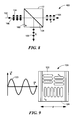
- FIG. 8 is a block diagram of which illustrates a operation of a polarizing beam splitter cube.
- FIG. 9 is a block diagram of a liquid crystal (LC) phase retarder.
- a switch 10 having an input 12 and a pair of outputs 14 , 16 includes a switchable high-power (HP) liquid crystal (LC) half-wave plate (HWP) 18 disposed at the input 12 and a polarizing beam splitter (PBS) disposed adjacent the HWP 12 .
- HP high-power
- LC liquid crystal
- PBS polarizing beam splitter
- switch 10 corresponds to a single input-two output switch (i.e. a 1 ⁇ 2 switch).
- switch 10 is capable of routing a high-power beam incident at the single input port 12 to either of the two output ports 14 , 16 .
- an incident polarized laser beam (designated with reference numeral 22 in FIG. 1 ) is passed through a switchable high-power (HP) liquid crystal (LC) half-wave plate (HWP), oriented with its fast axis at 45° to the input polarization direction and subsequently through polarizing beam splitter (PBS) 20 .
- HP high-power
- LC liquid crystal
- PBS polarizing beam splitter
- beams 22 , 24 , 26 are here illustrated as free-space beams; those of ordinary skill in the art will appreciate that any or all of beams 22 , 24 , 26 could equally well be provided as a beam from a fiber laser (e.g. an expanded, collimated beam from a fiber laser).
- the HWP in its “off” state converts an optical signal having a first polarization (designated as “p” polarization in FIG. 1 ) to a second polarization (designated as “s” polarization in FIG. 1 ).
- the HWP In its “on” state, the HWP is a null polarization operator (i.e. no polarization change is affected by the HWP).
- the nomenclature of “off” and “on” refers to the preferred embodiment of the HWP as a LCHWP, which becomes a null operator when voltage is applied but a fixed-orientation HWP when the voltage is off or at least much lower.
- the PBS is shown as a beam splitting cube.
- the PBS could equally be provided as an optical window coated with an appropriate dielectric thin film (an arrangement known as a polarizing plate with the plate oriented at the proper angle to effect the same polarization discrimination as a PBS).
- a PBS nominally passes light having a first polarization (e.g. the p polarized light in FIG. 1 ) and reflects (here downward) light having a second polarization (e.g. the s polarized light in FIG. 1 ).
- the HWP and PBS form a switching stage and when the HWP is on, p polarized input light is passed through this switching stage to the first output port. When the HWP is off the input p polarized light is converted to s and reflected downward to the second output port.
- each port is shown as a collimated free-space beam; however, for many high-power applications it is preferable to couple the output light to and from a fiber.
- a high power switch providing light signals to optical fibers 38 , 40 further includes a pair of optical phased arrays arranged as a tip/tilt/focus subsystem (TTFOPA) (i.e. two OPAs with their steering axes in different directions, preferably approximately perpendicular) provided at each port 14 , 16 and lenses 30 , 32 disposed to nominally focus output beams 24 , 26 for matching of a fiber mode to respective ones of the optical fibers 38 , 40 .
- TTFOPA tip/tilt/focus subsystem
- the TTFOPA disposed at each port provides for very fine angular (azimuth and elevation) and very fine focus adjustments to match the fiber mode to a relatively high accuracy.
- a single TTFOPA located upstream may be uses, as will be obvious to one of skill in the art.
- a pair of TTFOPAs may be used, to adjust both position and angle of the beams for optimum fiber coupling.
- Re-coupling light back into a fiber is a notoriously sensitive process; the focussed spot must be within a few microns of the desired longitudinal position and a fraction of a micron of the desired transverse position to couple efficiently to the fiber mode.
- the required angular settability of the TTFOPA is of the order of 10 ⁇ rad.
- a control loop circuit 42 (or more simply control circuit 42 ) is coupled between the output optical fiber 40 and the TTFOPA 32 .
- Control circuit 42 samples the power level in the output fiber 40 via coupler 44 and provides the sampled signal to a processor which in turn provides signals to TTFOPA to adjust the two TTFOPA angles and focal powers in two dimensions for maximum power coupled into fiber 40 . It should be appreciated that a similar control circuit can be provided at each additional output port.
- control circuit 42 comprises a coupler 44 (here shown as a directional coupler) 44 , a processor 46 and a signal path 48 .
- Coupler 44 couples a portion of light signals propagating in optical fiber 40 to an input of processor 46 and signal path 48 couples signals from an output of processor 46 to TTFOPA 32 .
- coupler 44 couples a portion of the light signal propagating in the output fiber 40 to an SPGD processor which performs a stochastic parallel gradient descent (SPGD) process on the signals provided thereto.
- SPOD processor then provides signals along signal path 46 to TTFOPA to adjust the two TTFOPA angles and focal powers in two dimensions for maximum power coupled into fiber 40 .
- SPGD stochastic parallel gradient descent
- HWP 18 and PBS 20 shown in FIGS. 1 and 2 comprise basic building blocks for switching fabrics, the cascading of which enables the creation of many other complex switching fabrics.
- embodiments may include a single TTFOPA, upstream of the HWP while other embodiments may include two TTFOPAs, either both upstream, both downstream, or one each.
- a switch 50 is provided from a plurality of, here M, switch stages 52 a - 52 M, generally denoted 52 .
- Switch 50 has an input 53 a and a plurality of outputs 54 a - 54 M and thus switch 50 is provided as a 1 ⁇ M switch.
- each switch stage 52 is comprised of a 1 ⁇ 2 switch element 10 (also sometimes referred to herein as elementary building blocks 10 or more simply building blocks 10 ).
- switch 50 is provided from a plurality of, here M, 1 ⁇ 2 switch elements 10 which may be the same as or similar to switch elements 10 described above in conjunction with FIGS. 1 and 2 .
- switch elements 10 are coupled to provide the 1 ⁇ M switch 50 .
- Switch 50 is capable of routing an optical signal provided to input 50 a to any of output ports 54 a - 54 M (i.e. M different output ports). It should be appreciated that in the exemplary embodiment of FIG. 3 , an example of switching between high-power optical fibers is shown, however, it should be understood that switch 50 is also capable of switching free space beams.
- switch 50 Operation of switch 50 can be explained as follows. Assume p polarized light is provided from a laser (not shown in FIG. 3 ) to switch input 53 a and coupled to switch a first switch stage 52 a . When HWP 1 of stage 52 a is ‘on’ its retardance is zero and the light remains p polarized and passes straight through PBS 1 to a first output port 54 a . When HWP 1 is ‘off’ its retardance is 180° and the polarization is transformed to s upon passage through HWP 1 , and the beam is consequently reflected downward from PBS 1 and into the second switching stage 52 b.
- HWP 2 in switch stage 52 b is off, the light remains s polarized and reflects from PBS 2 and exits port 54 b . If HWP 2 is ‘on’ the light is transformed to p polarization and passes through PBS 2 into the third switching stage 52 c , and so on. In this way M switching stages allow the light to be routed to any of M ports.
- Such a 1 ⁇ M switch is required if it is desired to route a centrally located high-power laser to multiple apertures distributed about the periphery of an aircraft.
- Some embodiments include an optional TTFOPA located upstream of the input near HWP 1 or downstream of the outputs (just upstream of the focussing lens), as described above in conjunction with FIG. 2 .
- embodiments may include a single TTFOPA, upstream of the HWP while other embodiments may include two TTFOPAs, either both upstream, both downstream, or one each.
- optical components such as cross-connect switches for example, can also be constructed from multiple units of the basic building block of FIG. 1 .
- FIG. 4 a cross connect switch is described. It should be noted that to promote clarity in the drawings and text a 2 ⁇ 2 cross connect 60 is described, but those of ordinary skill in the art will, after reading the description provided herein, appreciate that the same concepts may be applied to provide an N ⁇ N cross connect switch.
- the 2 ⁇ 2 cross connect 60 is provided if the input of a first 1 ⁇ 2 switch 50 ′, which may be the same as or similar to the type shown in FIG. 3 , is connected to port 1 ′ and a second 1 ⁇ M switch 50 ′′ of the same type is connected to port 2 ′, a 2 ⁇ M switch results.
- a switch can be used to implement redundancy.
- port 1 can be connected to either port 1 ′ or port 2 ′, and port 2 can likewise be connected to either of ports 1 ′ and 2 ′.
- HWP 1 on and HWP 3 both ‘on’, a p-polarized beam at port 1 is transmitted straight through to port 1 ′.
- HWP 1 and HWP 2 both ‘on’ and HWP 4 ‘off’, a p-polarized beam at port 1 is transmitted to port 2 ′ via two reflections and a transmission through PBS cubes 1 , 2 , and 4 . Switching from port 2 is accomplished similarly.
- a primary high-power laser connected to port 1 can be routed to any of the M ports of the 1 ⁇ M switch 50 ′. Should the primary laser fail, a backup high-power laser connected to port 2 of switch 50 ′′ can then be routed to any of the same M ports of the 1 ⁇ M switch.
- This is a so-called blocking switch: one can switch either port 1 or port 2 to port 1 ′ or port 2 ′, but not both simultaneously.
- a switch 70 having a so-called “non-blocking” switching architecture includes a first PBS 72 , a HWP 74 and a second PBS 76 disposed in an optical path.
- PBSs 72 , 76 and HWP 74 may be the same as or similar to PBS's and HWPs discussed above in conjunction with FIGS. 1-4 .
- Switch 70 allows simultaneous switching of port 1 and port 2 .
- port 1 can be connected to either port 1 ′ or port 2 ′, and port 2 can likewise be connected to either of ports 1 ′ and 2 ′.
- a p-polarized beam at port 1 is transmitted straight through to port 1 ′ and likewise an s-polarized beam at port 2 is reflected twice and transmitted thereby to port 2 ′.
- HWP 74 ‘on’ a p-polarized beam at port 1 is transmitted through PBS 72 and HWP 74 and reflected to port 2 ′ as an s polarized beam via PBS 76 .
- the s polarized input at Port 2 is changed to p polarization and is transmitted to port 1 ′.
- a first input laser beam having a p polarization and designated with reference numeral 77 in FIG. 5 can be coupled to either of switch port 1 ′ or switch port 2 ′ through switch 70 by properly biasing HWP 74 to its on or off states.
- Switching from port 2 is accomplished similarly. That is, with HWP 74 off′, an s-polarized beam at port 2 is first reflected via PBS 72 through HWP 74 to PBS 76 . PBS 76 which reflects the s polarized beam to port 2 ′. With HWP 74 ‘on’ an s-polarized beam at port 2 is reflected through PBS 72 to HWP 74 and is transmitted straight through PBS 76 to port 1 ′. Accordingly, a second input laser beam having a s polarization and designated with reference numeral 78 in FIG. 5 can be coupled to either of switch port 1 ′ or switch port 2 ′ through switch 70 by properly biasing HWP 74 to its on or off states.
- switches discussed above assume a polarized input beam. Not all beams, however, are polarized. Thus, switches for non-polarized light are described.
- switches for non-polarized light is that of laser pump diodes.
- One system architecture which utilizes centralized lasers and distributed apertures is centralized pump diodes distributed to multiple apertures, each with an associated gain medium.
- laser diode pump beams which are generally not polarized.
- FIGS. 6A and 6B illustrate a 1 ⁇ 2 switch 80 capable of operation with unpolarized light.
- an unpolarized input beam is split into s and p components at an input port 82 a of a PBS cube 82 .
- both signal components i.e. both the s and p components
- a first output port 82 b designated as “Aperture J, Array 1 ” in FIG. 6A ), and recombined.
- FIG. 6B shows the case of both HWPs “on,” in which case both of the s and p components are routed to a second output port 82 c (designated as “Aperture J, Array 2 ” in FIG. 6B ) where they are recombined.
- FIG. 6C shows an alternate embodiment in which when both HWPs are “off,” in which case both of the s and p components are muted to the second output port 82 c (designated as “Aperture 2 , Array 2 ” in FIG. 6C ) where they are recombined.
- an N ⁇ 2 switch 90 for switching unpolarized diode pumps (which are intended to be representative of any unpolarized laser source) is provided from a plurality of switch stages 92 (here N switch stages) each of which may be the same as or similar to a cascade of switches 70 described above in conjunction with the figure which replaces 6 .
- a plurality of laser sources here shown as N diode pumps 92 , are switched to one of first and second phased arrays 94 , 96 .
- switch 90 is arranged such that diode pump N is routed to the Nth aperture of either of first or second arrays, 94 , 96 .
- switch arrangements e.g. to route diode pump N to other apertures may be used.
- An incident beam 102 comprises components of both p (parallel to the plane of incidence, depicted with arrows generally denoted 104 ) and s (perpendicular to the plane of incidence, depicted with dots generally denoted 106 ) polarization.
- a diagonal interface 108 between the two right-angle prisms 110 , 112 is provided with a thin-film dielectric coating that allows p polarization to pass and s polarization to be reflected.
- switches are intended for use at or about standard laser wavelengths. Transmission through such a PBS is typically >95% for p polarization and reflection is >99% for s polarization. Note that the switch is arranged such that switching to port M requires M (low loss) s reflections but only a single (higher loss) p transmission.
- the entrance and exit faces are typically provided with high-quality antireflection coatings.
- Commercially available PBS' comprised of thin-film coated fused silica glass prisms, as an example, have laser damage thresholds typically of the order of 5 MW/cm 2 (cw) and 10 J/cm 2 (10 ns), which is more than adequate for the 1 to 50 kW (cw) power levels contemplated for this switch. See lasercomponents.com/us/product/mirror-coatings/ for typical performances.
- thin-film polarization plates can be used in place of the polarization beam splitting cubes. These have similar damage thresholds, but offer somewhat higher transmissions, especially for p polarization, where T>97% is routinely offered for high-power versions.
- the use of polarization plates instead of prisms can reduce the amount of glass in the optical path, which is beneficial for preservation of high beam quality, which is needed for efficient coupling into a single-mode fiber.
- variable HWP retarder as described herein is based upon liquid crystal (LC) technology, and is used primarily as a two-state switch.
- LC liquid crystal
- a phase retarder 120 comprises two transparent substrates, each provided with transparent, conducting thin-film electrodes and appropriate antireflection coatings, and a liquid crystal layer of appropriate thickness sandwiched between the substrates.
- the upper portion 122 illustrating the liquid crystals oriented such that an incident wave 123 sees an ordinary refractive index no (the voltage ‘on’ state); the lower portion 124 illustrates the liquid crystals oriented such that an incident wave sees the extraordinary refractive index n e (the voltage ‘off’ state).
- a HWP is constructed with sufficient LC thickness to provide a minimum of 180° retardance with zero applied voltage at a chosen wavelength. As the applied voltage is increased, the LC retardance decreases, and with sufficient voltage the retardance can be reduced effectively to zero.
- the necessary ‘on’ voltage is typically less than 10 V.
- the ‘on’ voltage may be on the order of 100V.
- a typical LC thickness for a HWP varies from a few microns to ten microns or so, depending upon the LC used.
- the so-called “fast axis” of the HWP is oriented at 45° to the polarization direction of the input beam, such that the HWP acts as a 90° polarization rotator when the retardance is 180° (the voltage ‘off’ state). With sufficient applied voltage to reduce the retardance to zero (the voltage ‘on’ state) the device passes arbitrary polarization without change.
- Phase retarders suitable for high-power operation have only recently been developed and demonstrated and in an Adaptive Photonic Phase Locked Element (APPLE).
- APPLE Adaptive Photonic Phase Locked Element
- High power operation in such phase retarders is achieved by: (1) reducing absorption losses of the transparent conducting thin-film electrodes; and (2) enabling efficient removal of thermal energy through the use of high thermal conductivity substrates such as sapphire substrates with an epitaxially grown gallium nitride (GaN) high electron mobility transistor (HEMT) layer that acts as a very efficient transparent conducting thin film.
- GaN gallium nitride
- HEMT high electron mobility transistor
- the combination of sapphire substrates and GaN HEMT layers has enabled the fabrication of wave plates having total absorption as low as 0.3%.
- An alternate substrate/thin-film system comprises indium oxide on either sapphire or spinel. Although the absorption loss is somewhat larger (about 1% per retarder), fabrication is simplified.
- phase retarders will exhibit neither exactly zero phase retardance when fully ‘on’, nor exactly 180° phase shift when ‘off’. Consequently, even if the input polarization is pure p polarized, the polarization of the beam as input to the PBS is not purely p or purely s, but instead contains a small amounts of the cross polarization. As a result the switch suffers from cross-port leakage.
- this switch It is the nature of this switch that there will be fairly high levels of cross-port power exchanges during switching transients. For instance, as the switch of FIG. 3 is reprogrammed to transfer energy from port 1 to port 3 , considerable energy can be transferred to port 2 during the finite switching times of the HWPs when the polarization state is neither completely s nor completely p. For applications where this is not acceptable, the input laser (with the term “input laser” used herein to mean any suitable light source) can be blanked for the duration of the switching transients.
- Polarizing beam splitting cubes are often used to fabricate low-power optical switches.
- the physical position of the output beam depends upon the polarization state of the input beam.
- a beam can be switched from one place to another.
- a high power phase retarder can be used as a high power polarization rotator, which in turn enables a wide variety of high power switches.
- the high power polarization rotator (switch) coupled with a high power polarizing beam splitter comprises a basic building block for optical switches (e.g. as shown and described in conjunction with FIG. 1 ).
- Described herein are systems, circuits and techniques to replace low-power components of well-known switching architectures with novel high power versions.
- the result is non-mechanical switches that not only handle high power, but are significantly less vibration sensitive (no moving parts), maintain alignment in harsh environments, have high throughput, and switch very fast (microseconds instead of milliseconds).
- the new switches also scale to large port numbers. These switches appear to have all the properties needed for our intended applications on aircraft, as well as other venues.
- the family of architectures of the switches to be claimed is well known for the low power regime.
- the novelty of at least some of the concepts described herein lies not necessarily in the switch architecture, but rather the in the means by which such well-known architectures can be emulated with novel high-power components (i.e. a high power wave plate and a polarizing beam splitter) which can be combined to enable high-power switches.
- novel high-power components i.e. a high power wave plate and a polarizing beam splitter
- one innovation of the concepts, systems and techniques described herein entails the application of a high power phase retarder, implemented as a polarization rotator, to enable operation of these same low-power switch architectures at power levels at least two to three orders of magnitude higher than has been previously possible.
Abstract
Description
Claims (26)
Priority Applications (1)
| Application Number | Priority Date | Filing Date | Title |
|---|---|---|---|
| US14/404,821 US9470953B2 (en) | 2012-05-24 | 2013-05-24 | High power optical switch |
Applications Claiming Priority (3)
| Application Number | Priority Date | Filing Date | Title |
|---|---|---|---|
| US201261651292P | 2012-05-24 | 2012-05-24 | |
| PCT/US2013/042641 WO2013177511A2 (en) | 2012-05-24 | 2013-05-24 | High power optical switch |
| US14/404,821 US9470953B2 (en) | 2012-05-24 | 2013-05-24 | High power optical switch |
Related Parent Applications (1)
| Application Number | Title | Priority Date | Filing Date |
|---|---|---|---|
| PCT/US2013/042641 A-371-Of-International WO2013177511A2 (en) | 2012-05-24 | 2013-05-24 | High power optical switch |
Related Child Applications (1)
| Application Number | Title | Priority Date | Filing Date |
|---|---|---|---|
| US15/152,592 Division US9772451B2 (en) | 2012-05-24 | 2016-05-12 | High power optical switch |
Publications (2)
| Publication Number | Publication Date |
|---|---|
| US20150185584A1 US20150185584A1 (en) | 2015-07-02 |
| US9470953B2 true US9470953B2 (en) | 2016-10-18 |
Family
ID=48570478
Family Applications (2)
| Application Number | Title | Priority Date | Filing Date |
|---|---|---|---|
| US14/404,821 Active US9470953B2 (en) | 2012-05-24 | 2013-05-24 | High power optical switch |
| US15/152,592 Active US9772451B2 (en) | 2012-05-24 | 2016-05-12 | High power optical switch |
Family Applications After (1)
| Application Number | Title | Priority Date | Filing Date |
|---|---|---|---|
| US15/152,592 Active US9772451B2 (en) | 2012-05-24 | 2016-05-12 | High power optical switch |
Country Status (6)
| Country | Link |
|---|---|
| US (2) | US9470953B2 (en) |
| EP (2) | EP2993517B1 (en) |
| AU (2) | AU2013266151B2 (en) |
| CA (2) | CA2874615C (en) |
| NZ (2) | NZ702303A (en) |
| WO (1) | WO2013177511A2 (en) |
Cited By (1)
| Publication number | Priority date | Publication date | Assignee | Title |
|---|---|---|---|---|
| US20160252796A1 (en) * | 2012-05-24 | 2016-09-01 | Raytheon Company | High Power Optical Switch |
Families Citing this family (8)
| Publication number | Priority date | Publication date | Assignee | Title |
|---|---|---|---|---|
| MX362849B (en) * | 2014-02-06 | 2019-02-19 | Nokia Technologies Oy | RECEPTION and GENERATION OF LIGHT. |
| US10036904B1 (en) * | 2014-03-26 | 2018-07-31 | Inphi Corporation | Method and system for integrated differential electro-absorption modulator device |
| CA2965174C (en) * | 2014-10-21 | 2023-10-10 | Reald Inc. | High power handling polarization switches |
| CN106646757B (en) * | 2017-03-07 | 2021-01-26 | 昂纳信息技术(深圳)有限公司 | Multiplexer and light combination method thereof |
| US10580084B1 (en) | 2017-10-11 | 2020-03-03 | State Farm Mutual Automobile Insurance Company | Recommendations to an operator of vehicle based upon vehicle usage detected by in-car audio signals |
| WO2019094254A1 (en) * | 2017-11-11 | 2019-05-16 | Hansen John Paul T | Optical networking devices and systems |
| JP2019124831A (en) * | 2018-01-17 | 2019-07-25 | パイオニア株式会社 | Irradiation device |
| CN109188700B (en) * | 2018-10-30 | 2021-05-11 | 京东方科技集团股份有限公司 | Optical display system and AR/VR display device |
Citations (29)
| Publication number | Priority date | Publication date | Assignee | Title |
|---|---|---|---|---|
| US4943709A (en) | 1989-05-11 | 1990-07-24 | Hughes Aircraft Company | Liquid crystal adaptive optics system |
| US4989941A (en) * | 1988-03-18 | 1991-02-05 | The United States Of America As Represented By The Secretary Of The Air Force | Normal incidence optical switches using ferroelectric liquid crystals |
| US5216729A (en) | 1991-11-18 | 1993-06-01 | Harmonic Lightwaves, Inc. | Active alignment system for laser to fiber coupling |
| US5253033A (en) | 1990-12-03 | 1993-10-12 | Raytheon Company | Laser radar system with phased-array beam steerer |
| US5276747A (en) | 1993-01-21 | 1994-01-04 | E-Tek Dynamics, Inc. | Polarization-independent optical switch/attenuator |
| US5363228A (en) | 1993-03-05 | 1994-11-08 | General Electric Company | Optical device with spatial light modulators for switching arbitrarily polarized light |
| US5404365A (en) | 1993-07-30 | 1995-04-04 | Fuji Photo Film Co., Ltd. | Polarized light coherent combining laser apparatus |
| US5740288A (en) | 1995-02-22 | 1998-04-14 | E-Tek Dynamics, Inc. | Variable polarization beam splitter, combiner and mixer |
| US5963682A (en) | 1994-05-24 | 1999-10-05 | Raytheon Company | Optical beam steering system |
| US6704474B1 (en) | 1994-05-24 | 2004-03-09 | Raytheon Company | Optical beam steering system |
| US6710736B2 (en) | 1999-06-14 | 2004-03-23 | Time Domain Corporation | System and method for intrusion detection using a time domain radar array |
| US20050018954A1 (en) | 2000-06-16 | 2005-01-27 | Bruno Vinouze | Liquid crystal optical switch with bumt-in control |
| US20060033995A1 (en) | 2004-08-12 | 2006-02-16 | Smith Irl W | Wide-angle beam steering system |
| US7006747B2 (en) | 2003-01-17 | 2006-02-28 | 3M Innovative Properties Company | Optical devices incorporating photo reactive polymers |
| US20060210219A1 (en) | 2005-03-16 | 2006-09-21 | Hitachi Cable, Ltd. | Optical transmitter |
| US20070014517A1 (en) | 2005-05-25 | 2007-01-18 | Biolase Technology, Inc. | Electromagnetic energy emitting device with increased spot size |
| US7196758B2 (en) | 2003-12-30 | 2007-03-27 | 3M Innovative Properties Company | Method of alignment of liquid crystals comprising exposing an alignment material to an interference pattern |
| US20070104417A1 (en) * | 2004-02-20 | 2007-05-10 | Dainichiseika Color & Chemicals Mfg. Co., Ltd. | Optically controlled optical-path-switching apparatus, and method of switching optical paths |
| US20090029071A1 (en) | 2005-12-15 | 2009-01-29 | Sei Hybrid Products, Inc | Transparent Spinel Substrate, Transparent Substrate for Optical Engine, Rear Projection Television Receiver Using Them and Image Projector Using Liquid Crystal |
| US20090142073A1 (en) | 2007-11-30 | 2009-06-04 | Smith Irl W | Method and apparatus for maintaining a coherent combined beam during arbitrary steering |
| US7570310B2 (en) | 2005-10-18 | 2009-08-04 | Fuji Xerox Co., Ltd. | Method for driving optical address type spatial light modulation device and apparatus for driving optical address type spatial light modulation device |
| US7692759B2 (en) | 2005-03-01 | 2010-04-06 | Stichting Dutch Polymer Institute | Polarization gratings in mesogenic films |
| US7848370B2 (en) | 2007-01-26 | 2010-12-07 | Telaris Inc. | Electronically phase-locked laser systems |
| US20100320474A1 (en) | 2009-06-22 | 2010-12-23 | Raytheon Company | Gallium nitride for liquid crystal electrodes |
| US7889767B2 (en) | 2004-10-13 | 2011-02-15 | Raytheon Company | Self-coherent combining technique for high power laser implementation and method |
| US7990600B2 (en) | 2004-05-24 | 2011-08-02 | Compound Photonics Limited | Transmissive, optically addressed, photosensitive spatial light modulators and color display systems incorporating same |
| US20120081621A1 (en) | 2010-10-01 | 2012-04-05 | Raytheon Company | High Fill-Factor Electronic Beam Steerer |
| US20140268328A1 (en) | 2013-03-13 | 2014-09-18 | Raytheon Company | Polarization Grating Stack |
| US20150185584A1 (en) * | 2012-05-24 | 2015-07-02 | Raytheon Company | High Power Optical Switch |
Family Cites Families (11)
| Publication number | Priority date | Publication date | Assignee | Title |
|---|---|---|---|---|
| US5241610A (en) * | 1991-09-03 | 1993-08-31 | Scientific-Atlanta, Inc. | Optical switching in a fiber communication system and method using same |
| US5381250A (en) * | 1992-11-06 | 1995-01-10 | Displaytech, Inc. | Electro-optical switch with 4 port modules with electro-optic polarization rotators |
| US6341118B1 (en) * | 1998-06-02 | 2002-01-22 | Science Applications International Corporation | Multiple channel scanning device using oversampling and image processing to increase throughput |
| US6366714B1 (en) * | 1998-06-19 | 2002-04-02 | Corning Incorporated | High reliability fiber coupled optical switch |
| US6643423B2 (en) * | 2001-05-08 | 2003-11-04 | Nortel Networks Limited | System and method for bridge and roll in a photonic switch |
| US6898342B2 (en) * | 2002-08-08 | 2005-05-24 | Intel Corporation | Fiber-aligning optical switch |
| US6920258B2 (en) * | 2002-10-03 | 2005-07-19 | Hon Hai Precision Ind. Co., Ltd. | Optical switch |
| US7263250B1 (en) * | 2002-10-18 | 2007-08-28 | Finisar Corporation | Optical switch using polarization beam splitters |
| US7298565B2 (en) * | 2004-10-22 | 2007-11-20 | Ac Photonics | Compact and high performance opto-mechanical switch |
| EP2394190A4 (en) * | 2009-02-03 | 2018-04-25 | Winchester Electronics Corporation | Fiber optic jack and connector |
| KR101320592B1 (en) * | 2009-11-19 | 2013-10-23 | (주)켐옵틱스 | Optical communication device haiving digital optical switchs |
-
2013
- 2013-05-24 EP EP15191517.0A patent/EP2993517B1/en active Active
- 2013-05-24 NZ NZ702303A patent/NZ702303A/en unknown
- 2013-05-24 AU AU2013266151A patent/AU2013266151B2/en active Active
- 2013-05-24 CA CA2874615A patent/CA2874615C/en active Active
- 2013-05-24 WO PCT/US2013/042641 patent/WO2013177511A2/en active Application Filing
- 2013-05-24 NZ NZ717901A patent/NZ717901A/en unknown
- 2013-05-24 US US14/404,821 patent/US9470953B2/en active Active
- 2013-05-24 CA CA2926296A patent/CA2926296C/en active Active
- 2013-05-24 EP EP13726661.5A patent/EP2856253B1/en active Active
-
2015
- 2015-10-21 AU AU2015246091A patent/AU2015246091B2/en active Active
-
2016
- 2016-05-12 US US15/152,592 patent/US9772451B2/en active Active
Patent Citations (32)
| Publication number | Priority date | Publication date | Assignee | Title |
|---|---|---|---|---|
| US4989941A (en) * | 1988-03-18 | 1991-02-05 | The United States Of America As Represented By The Secretary Of The Air Force | Normal incidence optical switches using ferroelectric liquid crystals |
| US4943709A (en) | 1989-05-11 | 1990-07-24 | Hughes Aircraft Company | Liquid crystal adaptive optics system |
| US5253033A (en) | 1990-12-03 | 1993-10-12 | Raytheon Company | Laser radar system with phased-array beam steerer |
| US5216729A (en) | 1991-11-18 | 1993-06-01 | Harmonic Lightwaves, Inc. | Active alignment system for laser to fiber coupling |
| US5276747A (en) | 1993-01-21 | 1994-01-04 | E-Tek Dynamics, Inc. | Polarization-independent optical switch/attenuator |
| US5363228A (en) | 1993-03-05 | 1994-11-08 | General Electric Company | Optical device with spatial light modulators for switching arbitrarily polarized light |
| US5404365A (en) | 1993-07-30 | 1995-04-04 | Fuji Photo Film Co., Ltd. | Polarized light coherent combining laser apparatus |
| US5963682A (en) | 1994-05-24 | 1999-10-05 | Raytheon Company | Optical beam steering system |
| US6704474B1 (en) | 1994-05-24 | 2004-03-09 | Raytheon Company | Optical beam steering system |
| US5740288A (en) | 1995-02-22 | 1998-04-14 | E-Tek Dynamics, Inc. | Variable polarization beam splitter, combiner and mixer |
| US6710736B2 (en) | 1999-06-14 | 2004-03-23 | Time Domain Corporation | System and method for intrusion detection using a time domain radar array |
| US20050018954A1 (en) | 2000-06-16 | 2005-01-27 | Bruno Vinouze | Liquid crystal optical switch with bumt-in control |
| US7006747B2 (en) | 2003-01-17 | 2006-02-28 | 3M Innovative Properties Company | Optical devices incorporating photo reactive polymers |
| US7196758B2 (en) | 2003-12-30 | 2007-03-27 | 3M Innovative Properties Company | Method of alignment of liquid crystals comprising exposing an alignment material to an interference pattern |
| US20070104417A1 (en) * | 2004-02-20 | 2007-05-10 | Dainichiseika Color & Chemicals Mfg. Co., Ltd. | Optically controlled optical-path-switching apparatus, and method of switching optical paths |
| US7990600B2 (en) | 2004-05-24 | 2011-08-02 | Compound Photonics Limited | Transmissive, optically addressed, photosensitive spatial light modulators and color display systems incorporating same |
| US7428100B2 (en) | 2004-08-12 | 2008-09-23 | Raytheon Company | Wide-angle beam steering system |
| US20060033995A1 (en) | 2004-08-12 | 2006-02-16 | Smith Irl W | Wide-angle beam steering system |
| US7215472B2 (en) | 2004-08-12 | 2007-05-08 | Raytheon Company | Wide-angle beam steering system |
| US7889767B2 (en) | 2004-10-13 | 2011-02-15 | Raytheon Company | Self-coherent combining technique for high power laser implementation and method |
| US7692759B2 (en) | 2005-03-01 | 2010-04-06 | Stichting Dutch Polymer Institute | Polarization gratings in mesogenic films |
| US20060210219A1 (en) | 2005-03-16 | 2006-09-21 | Hitachi Cable, Ltd. | Optical transmitter |
| US20070014517A1 (en) | 2005-05-25 | 2007-01-18 | Biolase Technology, Inc. | Electromagnetic energy emitting device with increased spot size |
| US7570310B2 (en) | 2005-10-18 | 2009-08-04 | Fuji Xerox Co., Ltd. | Method for driving optical address type spatial light modulation device and apparatus for driving optical address type spatial light modulation device |
| US20090029071A1 (en) | 2005-12-15 | 2009-01-29 | Sei Hybrid Products, Inc | Transparent Spinel Substrate, Transparent Substrate for Optical Engine, Rear Projection Television Receiver Using Them and Image Projector Using Liquid Crystal |
| US7848370B2 (en) | 2007-01-26 | 2010-12-07 | Telaris Inc. | Electronically phase-locked laser systems |
| US20090142073A1 (en) | 2007-11-30 | 2009-06-04 | Smith Irl W | Method and apparatus for maintaining a coherent combined beam during arbitrary steering |
| US20100320474A1 (en) | 2009-06-22 | 2010-12-23 | Raytheon Company | Gallium nitride for liquid crystal electrodes |
| US8268707B2 (en) | 2009-06-22 | 2012-09-18 | Raytheon Company | Gallium nitride for liquid crystal electrodes |
| US20120081621A1 (en) | 2010-10-01 | 2012-04-05 | Raytheon Company | High Fill-Factor Electronic Beam Steerer |
| US20150185584A1 (en) * | 2012-05-24 | 2015-07-02 | Raytheon Company | High Power Optical Switch |
| US20140268328A1 (en) | 2013-03-13 | 2014-09-18 | Raytheon Company | Polarization Grating Stack |
Non-Patent Citations (45)
| Title |
|---|
| "Liquid crystal blazed-grating beam deflector," by Wang et al, Applied Optics, vol. 39, No. 35, pp. 6545-6555, 2000. |
| Australian Office Action dated May 28, 2015 for Appl. No. 2013266151. |
| Crawford, et al.; "Internal surface, orientational order, and distribution of a polymer network in a liquid crystal matrix;" Physical Review E; Rapid Communications; The American Physical Society; vol. 52; No. 2; Aug. 1995; pp. R1273-R1276. |
| Dorschner; "Adaptive Photonic Phase Locked Elements;" An Overview; DARPA/MTO Symposium; Mar. 2007; pp. 1-15. |
| Examiner's Report dated Nov. 27, 2015 for Appl. No. 2,874,615; 4 pages. |
| Fan et al.; "Fast-Response and scattering-free polymer network liquid crystals for infrared light modulators;" Applied Physics Letters; American Institute of Physics; vol. 84; No. 8; Feb. 23, 2004; pp. 1233-1235. |
| Further Examination Report filed in New Zealand Intellectual Property Office for Appl. No. 702303 dated Oct. 20, 2015; 3 pages. |
| Further Examination Report Postponed Acceptance dated Feb. 1, 2016 for New Zealand Appl. No. 702303; 1 page. |
| Gelissen et al.; "Polarization Control Using Nematic Liquid Crystals;" Advances in Optical Information Processing; Proceedings of SPIE vol. 4046; Apr. 25, 2000; pp. 118-129. |
| International Preliminary Report on Patentability of the ISA for PCT/US2011/054245 dated Apr. 11, 2013. |
| Kim, et al.; "Wide-angle, nonmechanical beam steering using thin liquid crystal polarization gratings;" Proc. of SPIE; vol. 7093; Jan. 2008, pp. 1-12. |
| McManamon, et al., "Optical Phased Array Technology;" Proceedings of the IEEE; vol. 84; No. 2; Feb. 1996; pp. 268-298. |
| McManamon, et al.; "A Review of Phased Array Steering for Narrow-Band Electrooptical System;" Proceeding of the IEEE; vol. 97; No. 6; Jun. 2009; pp. 1078-1096. |
| Miller; Self-aligning universal beam coupler; Optics Express; vol. 21; No. 5; Mar. 11, 2013; pp. 6360-6370. |
| New Zealand Office Action dated Mar. 24, 2015 for Appl. No. 702303; 3 pages. |
| Nicolescu, et al.; "Polarization-independent tunable optical filters based on liquid crystal polarization gratings;" Proceedings of SPIE; vol. 6654; No. 665405; Aug. 2007; 12 pages. |
| Office Action dated Feb. 21, 2013 from U.S. Appl. No. 13/250,111. |
| Office Action dated Sep. 6, 2013 from U.S. Appl. No. 13/250,111. |
| Partial PCT Search Report received with Invitation to Pay Additional Fees in PCT/US2011/054245 dated Jan. 18, 2012. |
| PCT International Preliminary Report on Patentability for PCT/US2013/042641 dated Dec. 4, 2014 11 pages. |
| PCT International Preliminary Report on Patentability for PCT/US2013/042646 dated May 24, 2013 6 pages. |
| PCT International Preliminary Report on Patentability for PCT/US2013/042653 dated May 24, 2013 10 pages. |
| PCT Invitation to Pay Additional Fees for PCT/US2013/042641 dated Sep. 20, 2013 10 pages. |
| PCT Search Report of the ISA for PCT/US2011/054245 dated Mar. 26, 2012. |
| PCT Search Report of the ISA for PCT/US2013/042641 dated Jan. 30, 2014 9 pages. |
| PCT Search Report of the ISA for PCT/US2013/042646 dated Sep. 3, 2013 5 pages. |
| PCT Search Report of the ISA for PCT/US2013/042653 dated Nov. 7, 2013 6 pages. |
| Ren et al.; "Tunable Microlens arrays using polymer network liquid crystal;" Optics Communications; Science Direct; Sep. 22, 2003; pp. 267-271. |
| Response to Australian Office Action as filed on Sep. 28, 2015 for Appl. No. 2013266151; 29 pages. |
| Response to Examination Report dated Oct. 20, 2015 as filed on Dec. 22, 2015 for New Zealand Appl. No. 702303; 53 pages. |
| Response to Examner's Report dated Nov. 27, 2015 for Canadian Application No. 2874615 as fled on Apr. 1, 2016; 23 pages. |
| Response to Office Action dated Feb. 21, 2013 as filed on May 16, 2013 from U.S. Appl. No. 13/250,111. |
| Response to Rule 161 Communication for Application No. 11770009.6 as filed on Dec. 23, 2013. |
| Response to Rule 161(1) and 162 EPC Communication filed on Jul. 22, 2015 for EP Application No. 13726661.5. |
| Response to the Office Action for Appl. No. 702303 filed in New Zealand Intellectual Property Office on Sep. 22, 2015; 61 pages. |
| Rockwell, et al.; "Semi-guiding high-aspect-ratio-core (SHARC) fiber providing single-mode operation and an ultra-large core area in a compact coliable package;" Optics Express; vol. 19; No. 15; Jul. 18, 2011; pp. 14746-14762. |
| Rule 161 Communication for Application No. 11770009.6 dated Jun. 12, 2013. |
| U.S. Appl. No. 13/250,111, filed Sep. 30, 2011. |
| U.S. Appl. No. 13/801,411, filed Mar. 13, 2013. |
| Voluntary Amendment as filed Mar. 3, 2016 for Australian Application No. 2015246091; 54 pages. |
| Wang, et al.; "Stressed liquid-crystal optical phased array for fast tip-tilt wavefront correction;" Applied Optics; vol. 44; No. 36; Dec. 20, 2005; pp. 7754-7759. |
| Written Opinion of the ISA for PCT/US2011/054245 dated Mar. 26, 2012. |
| Written Opinion of the ISA for PCT/US2013/042641 dated Jan. 30, 2014 9 pages. |
| Written Opinion of the ISA for PCT/US2013/042646 dated Sep. 3, 2013 4 pages. |
| Written Opinion of the ISA for PCT/US2013/042653 dated Nov. 7, 2013 9 pages. |
Cited By (2)
| Publication number | Priority date | Publication date | Assignee | Title |
|---|---|---|---|---|
| US20160252796A1 (en) * | 2012-05-24 | 2016-09-01 | Raytheon Company | High Power Optical Switch |
| US9772451B2 (en) * | 2012-05-24 | 2017-09-26 | Raytheon Company | High power optical switch |
Also Published As
| Publication number | Publication date |
|---|---|
| AU2013266151A1 (en) | 2014-12-18 |
| EP2993517B1 (en) | 2018-06-20 |
| NZ702303A (en) | 2016-03-31 |
| AU2015246091B2 (en) | 2017-03-09 |
| AU2013266151B2 (en) | 2015-11-12 |
| CA2926296A1 (en) | 2013-11-28 |
| EP2856253A2 (en) | 2015-04-08 |
| US20160252796A1 (en) | 2016-09-01 |
| US20150185584A1 (en) | 2015-07-02 |
| NZ717901A (en) | 2017-07-28 |
| EP2856253B1 (en) | 2016-08-24 |
| WO2013177511A2 (en) | 2013-11-28 |
| US9772451B2 (en) | 2017-09-26 |
| CA2926296C (en) | 2019-01-29 |
| CA2874615A1 (en) | 2013-11-28 |
| AU2015246091A1 (en) | 2015-11-05 |
| WO2013177511A3 (en) | 2014-03-13 |
| EP2993517A1 (en) | 2016-03-09 |
| CA2874615C (en) | 2017-09-19 |
Similar Documents
| Publication | Publication Date | Title |
|---|---|---|
| US9772451B2 (en) | High power optical switch | |
| CN109765658B (en) | 2x2 wavelength selective switch array | |
| US6690854B2 (en) | Optical wavelength division multiplexer | |
| US6983097B2 (en) | Magneto-optical switching backplane for processor interconnection | |
| US10267994B2 (en) | Wavelength selective switch including a liquid crystal on silicon | |
| EP3465303B1 (en) | Optical coupling device and method | |
| US10474001B2 (en) | Wavelength selection switch including a switching module having a liquid crystal phase array, a polarizer and a liquid crystal on silicon | |
| US20050174919A1 (en) | Optical polarization controller | |
| US8094982B2 (en) | Fiber lens assembly for optical device | |
| US7263250B1 (en) | Optical switch using polarization beam splitters | |
| WO2019203307A1 (en) | Wavelength-selective optical switch | |
| US7079319B2 (en) | Optical signal control device and method for utilizing same | |
| WO2023142530A1 (en) | Polarization-independent device and apparatus, and optical network system | |
| US20230288738A1 (en) | Integrated isolator and circulator systems | |
| JP2848836B2 (en) | Optical splitter | |
| Soref | Fiber-Optic Switching With Liquid Crystals | |
| Kudo et al. | Waveguide-frontend with integrated polarization diversity optics for wavelength selective switch array |
Legal Events
| Date | Code | Title | Description |
|---|---|---|---|
| AS | Assignment |
Owner name: RAYTHEON COMPANY, MASSACHUSETTS Free format text: ASSIGNMENT OF ASSIGNORS INTEREST;ASSIGNORS:SMITH, IRL W.;DORSCHNER, TERRY A.;REEL/FRAME:034523/0565 Effective date: 20141211 |
|
| STCF | Information on status: patent grant |
Free format text: PATENTED CASE |
|
| MAFP | Maintenance fee payment |
Free format text: PAYMENT OF MAINTENANCE FEE, 4TH YEAR, LARGE ENTITY (ORIGINAL EVENT CODE: M1551); ENTITY STATUS OF PATENT OWNER: LARGE ENTITY Year of fee payment: 4 |
|
| MAFP | Maintenance fee payment |
Free format text: PAYMENT OF MAINTENANCE FEE, 8TH YEAR, LARGE ENTITY (ORIGINAL EVENT CODE: M1552); ENTITY STATUS OF PATENT OWNER: LARGE ENTITY Year of fee payment: 8 |