US9484269B2 - Structure and method to control bottom corner threshold in an SOI device - Google Patents
Structure and method to control bottom corner threshold in an SOI device Download PDFInfo
- Publication number
- US9484269B2 US9484269B2 US12/822,492 US82249210A US9484269B2 US 9484269 B2 US9484269 B2 US 9484269B2 US 82249210 A US82249210 A US 82249210A US 9484269 B2 US9484269 B2 US 9484269B2
- Authority
- US
- United States
- Prior art keywords
- trench
- doping
- soi
- layer
- corner region
- Prior art date
- Legal status (The legal status is an assumption and is not a legal conclusion. Google has not performed a legal analysis and makes no representation as to the accuracy of the status listed.)
- Active, expires
Links
Images


Classifications
-
- H—ELECTRICITY
- H01—ELECTRIC ELEMENTS
- H01L—SEMICONDUCTOR DEVICES NOT COVERED BY CLASS H10
- H01L21/00—Processes or apparatus adapted for the manufacture or treatment of semiconductor or solid state devices or of parts thereof
- H01L21/70—Manufacture or treatment of devices consisting of a plurality of solid state components formed in or on a common substrate or of parts thereof; Manufacture of integrated circuit devices or of parts thereof
- H01L21/77—Manufacture or treatment of devices consisting of a plurality of solid state components or integrated circuits formed in, or on, a common substrate
- H01L21/78—Manufacture or treatment of devices consisting of a plurality of solid state components or integrated circuits formed in, or on, a common substrate with subsequent division of the substrate into plural individual devices
- H01L21/82—Manufacture or treatment of devices consisting of a plurality of solid state components or integrated circuits formed in, or on, a common substrate with subsequent division of the substrate into plural individual devices to produce devices, e.g. integrated circuits, each consisting of a plurality of components
- H01L21/84—Manufacture or treatment of devices consisting of a plurality of solid state components or integrated circuits formed in, or on, a common substrate with subsequent division of the substrate into plural individual devices to produce devices, e.g. integrated circuits, each consisting of a plurality of components the substrate being other than a semiconductor body, e.g. being an insulating body
-
- H—ELECTRICITY
- H01—ELECTRIC ELEMENTS
- H01L—SEMICONDUCTOR DEVICES NOT COVERED BY CLASS H10
- H01L21/00—Processes or apparatus adapted for the manufacture or treatment of semiconductor or solid state devices or of parts thereof
- H01L21/70—Manufacture or treatment of devices consisting of a plurality of solid state components formed in or on a common substrate or of parts thereof; Manufacture of integrated circuit devices or of parts thereof
- H01L21/71—Manufacture of specific parts of devices defined in group H01L21/70
- H01L21/76—Making of isolation regions between components
- H01L21/762—Dielectric regions, e.g. EPIC dielectric isolation, LOCOS; Trench refilling techniques, SOI technology, use of channel stoppers
- H01L21/76224—Dielectric regions, e.g. EPIC dielectric isolation, LOCOS; Trench refilling techniques, SOI technology, use of channel stoppers using trench refilling with dielectric materials
- H01L21/76237—Dielectric regions, e.g. EPIC dielectric isolation, LOCOS; Trench refilling techniques, SOI technology, use of channel stoppers using trench refilling with dielectric materials introducing impurities in trench side or bottom walls, e.g. for forming channel stoppers or alter isolation behavior
-
- H01L27/10847—
-
- H—ELECTRICITY
- H01—ELECTRIC ELEMENTS
- H01L—SEMICONDUCTOR DEVICES NOT COVERED BY CLASS H10
- H01L27/00—Devices consisting of a plurality of semiconductor or other solid-state components formed in or on a common substrate
- H01L27/02—Devices consisting of a plurality of semiconductor or other solid-state components formed in or on a common substrate including semiconductor components specially adapted for rectifying, oscillating, amplifying or switching and having at least one potential-jump barrier or surface barrier; including integrated passive circuit elements with at least one potential-jump barrier or surface barrier
- H01L27/12—Devices consisting of a plurality of semiconductor or other solid-state components formed in or on a common substrate including semiconductor components specially adapted for rectifying, oscillating, amplifying or switching and having at least one potential-jump barrier or surface barrier; including integrated passive circuit elements with at least one potential-jump barrier or surface barrier the substrate being other than a semiconductor body, e.g. an insulating body
- H01L27/1203—Devices consisting of a plurality of semiconductor or other solid-state components formed in or on a common substrate including semiconductor components specially adapted for rectifying, oscillating, amplifying or switching and having at least one potential-jump barrier or surface barrier; including integrated passive circuit elements with at least one potential-jump barrier or surface barrier the substrate being other than a semiconductor body, e.g. an insulating body the substrate comprising an insulating body on a semiconductor body, e.g. SOI
-
- H—ELECTRICITY
- H10—SEMICONDUCTOR DEVICES; ELECTRIC SOLID-STATE DEVICES NOT OTHERWISE PROVIDED FOR
- H10B—ELECTRONIC MEMORY DEVICES
- H10B12/00—Dynamic random access memory [DRAM] devices
- H10B12/01—Manufacture or treatment
- H10B12/02—Manufacture or treatment for one transistor one-capacitor [1T-1C] memory cells
Definitions
- the invention relates to a semiconductor structures and methods of manufacture and, more particularly, a structure and method to control bottom corner threshold in a silicon-on-insulator (SOI) device.
- SOI silicon-on-insulator
- a deep trench (DT) gating effect may exist in an array of eDRAM devices and is a prominent leakage mechanism that reduces the retention time of eDRAM devices.
- each device may comprise a storage cell (e.g., a deep trench capacitor) and a gate (e.g., a FET).
- the storage cell of one device may electrically couple with the SOI island in which a FET of an adjacent device is formed. This capacitive coupling between the storage cell of one eDRAM and the SOI island of a FET of an adjacent eDRAM weakly turns on the surface at the back or bottom corner of the SOI island that the adjacent FET is formed on, which creates a leakage current in the adjacent FET.
- the leakage current causes the adjacent eDRAM to lose its charge, e.g., the information stored in its storage cell.
- Such leakage necessitates more frequent refreshing which is undesirable for a number of reasons, including the fact that more frequent refreshing consumes more power.
- a technique for reducing DT gating is to increase the spacing between the storage cells and the gates of adjacent devices.
- increasing the spacing between devices goes against the constant drive in the industry for reducing the size of integrated circuits.
- Another way to address DT gating is by performing halo implants, through-gate implants, and/or well implants at the FET.
- implant techniques result in doping the entire backside and/or entire sidewall of the SOI island in which the FET is formed, and such over-doping can negatively affect device performance in an undesired manner.
- a method of fabricating a semiconductor structure includes doping a corner region of a semiconductor-on-insulator (SOI) island.
- the doping includes tailoring a localized doping of the corner region to reduce capacitive coupling of the SOI island with an adjacent structure.
- the method includes: forming a trench in a semiconductor-on-insulator (SOI) wafer; exposing a surface of a corner region of an SOI island via the trench; and doping the corner region of the SOI island through the exposed surface.
- SOI semiconductor-on-insulator
- a semiconductor device including: a substrate; a buried insulator layer on the substrate; and a semiconductor-on-insulator (SOI) island on the buried insulator layer.
- the semiconductor device also includes a structure in the buried insulator layer adjacent the SOI island, the structure being connected to a non-zero voltage during at least a portion of device operation.
- the semiconductor device also includes an isolation region between the SOI island and the structure, wherein one or more corner regions of the SOI island comprise a localized doping that reduces capacitive coupling between the SOI island and the structure.
- FIGS. 1 and 2 show structures associated with aspects of the invention
- FIGS. 3-6 show processing steps and structures associated with aspects of the invention
- FIG. 7 shows corner doping concentrations associated with FIGS. 3-6 in accordance with aspects of the invention.
- FIGS. 8-13 show processing steps and structures associated with aspects of the invention.
- FIG. 14 shows corner doping concentrations associated with FIGS. 8-13 in accordance with aspects of the invention.
- FIG. 15 is a flow diagram of a design process used in semiconductor design, manufacture, and/or test.
- the invention relates to a semiconductor structures and methods of manufacture and, more particularly, a structure and method to control bottom corner threshold in a silicon-on-insulator (SOI) device.
- SOI silicon-on-insulator
- a localized doping is performed at the bottom corner of an SOI island associated with an eDRAM FET.
- the localized doping in the bottom corner of the SOI island reduces the gating effect by preventing the capacitive coupling between the SOI island and an adjacent eDRAM storage cell.
- FIG. 1 shows an array of eDRAM devices in accordance with aspects of the invention.
- Each individual device in the array may include, among other features, a storage cell, a gate, and a contact.
- a first device may comprise a storage cell 15 a , a gate 20 a , and a contact 25 a .
- a second device may comprise a storage cell 15 b , a gate 20 b , and a contact 25 b .
- a third device may comprise a storage cell 15 c , a gate 20 c , and a contact 25 c .
- Any number of devices may be used within the array 10 , and the devices may be arranged in any desired pattern.
- the device may be staggered in the array 10 such that the gates 20 a and 20 c of a first and third device are adjacent to the storage cell 15 b of a second device.
- FIG. 2 shows a cross section of the wafer containing the array 10 taken along line II-II of FIG. 1 .
- the wafer includes a substrate 30 , a buried insulator layer 35 on the substrate 30 , and SOI islands 40 formed in the insulator layer 35 .
- the gates 20 a and 20 c of the first and third devices are formed in the SOI islands 40 , which are in close proximity to the storage cell 15 b of the second device.
- the storage cell 15 b comprises a deep trench (DT) capacitor that extends through the insulator layer 35 into the substrate 30 .
- the elements depicted in FIG. 2 may be of any suitable size.
- the storage cell 15 b may comprise a width of about 160 nm to about 178 nm; however, the invention is not limited to these dimensions, and any suitable dimensions may be used within the scope of the invention.
- the SOI islands 40 may have widths ranging from about 76 nm to about 86 nm; however, the invention is not limited to these dimensions, and any suitable dimensions may be used within the scope of the invention.
- the bottom corners 45 of the SOI islands 40 are doped to prevent this capacitive coupling “C” and therefore to reduce or eliminate the gating effect. As described in greater detail herein, in embodiments the doping is performed in a localized manner at the corner 45 , such that doping of entire sides of the SOI island 40 is avoided.
- FIGS. 3-6 and 8-14 show processing steps and structures associated with forming a semiconductor device in accordance with aspects of the invention.
- FIG. 3 shows an exemplary SOI wafer employed as an intermediate structure in implementations of the invention.
- the SOI wafer has a bulk semiconductor substrate 30 ′, which is typically a silicon substrate, a buried insulator layer 35 ′ formed on the substrate 30 ′, and a semiconductor layer 37 , which is typically a silicon layer, formed on the buried insulator layer 35 ′.
- the substrate 30 ′ and buried insulator layer 35 ′ may be similar to the substrate 30 and insulator layer 35 , respectively, described above with respect to FIG. 2 .
- the SOI wafer may be fabricated using techniques well know to those skilled in the art.
- the SOI wafer may be formed by conventional processes including, but not limited to, oxygen implantation (e.g., SIMOX), wafer bonding (e.g., the “SMART CUT” method, which is a registered trademark of S.O.I.TEC Silicon On Insulator Technologies of Bernin, France), etc.
- oxygen implantation e.g., SIMOX
- wafer bonding e.g., the “SMART CUT” method, which is a registered trademark of S.O.I.TEC Silicon On Insulator Technologies of Bernin, France
- the constituent materials of the SOI wafer may be selected based on the desired end use application of the semiconductor device.
- the substrate 30 ′ may be composed of any suitable material including, but not limited to, Si, SiGe, SiGeC, SiC, GE alloys, GaAs, InAs, InP, and other III/V or II/VI compound semiconductors.
- the buried insulator layer 35 ′ may be composed of oxide, such as SiO 2 , and may be referred to as a buried oxide (BOX) layer 35 ′.
- the SOI wafer is referred to as “silicon on insulator,” the semiconductor layer 37 is not limited to silicon. Instead, the semiconductor layer 37 may be comprised of various semiconductor materials, such as, for example, Si, SiGe, SiC, SiGeC, etc.
- the SOI wafer has a thickness of about 700 ⁇ m, with the BOX layer 35 ′ having a thickness of about 0.14 ⁇ m, and the semiconductor layer 37 having a thickness of about 0.08 ⁇ m.
- the invention is not limited to these dimensions, and the various portions of the SOI wafer may have any desired thicknesses based upon the intended use of the final semiconductor device.
- FIG. 4 shows a portion of the wafer after a number of conventional semiconductor fabrication processing steps have been performed, including: forming a deep trench capacitor 50 in the wafer; forming a layer of pad oxide 55 on the upper surface of the wafer; forming a layer of pad nitride 60 on the pad oxide 55 ; forming a trench 65 through the pad nitride 60 , pad oxide 55 , and semiconductor layer 37 down to the BOX layer 35 ′; and forming a liner 70 on the sidewalls of the trench 65 while leaving at least a portion of the upper surface of the BOX layer 35 ′ exposed.
- element 50 may be any adjacent structure that is connected to some certain voltage during the device operation and generates coupling effects.
- element 50 may comprise a deep trench capacitor, another FET, a buried conducting wire (e.g. wordline or bitline), etc.
- the pad oxide 55 and pad nitride 60 may comprise any suitable oxide and nitride, respectively, such as SiO 2 and Si 3 N 4 , and may be formed using any desired fabrication technique, such as: thermal oxidation, chemical oxidation, thermal nitridation, atomic layer deposition (ALD), molecular layer deposition (MLD), chemical vapor deposition (CVD), low-pressure chemical vapor deposition (LPCVD), plasma enhanced chemical vapor deposition (PECVD), etc.
- ALD atomic layer deposition
- MLD molecular layer deposition
- CVD chemical vapor deposition
- LPCVD low-pressure chemical vapor deposition
- PECVD plasma enhanced chemical vapor deposition
- the trench 65 may be formed using any suitable semiconductor fabrication techniques, including but not limited to: masking and etching, laser ablation, gas cluster ion beam, etc.
- the trench 65 is formed by applying a patterned mask (not shown) on the structure and removing material of the pad nitride 60 , pad oxide 55 , and semiconductor layer 37 through the patterned mask via one or more etch processes.
- the mask may be composed of, for example, a photoresist material, a hard mask material, or any other suitable masking layer.
- the one or more etch processes are anisotropic so that the etching occurs in a substantially vertical direction.
- the trench 65 may have a depth of about 0.08 ⁇ m and a width of about 60 nm, although the invention is not limited to these values and any size trench may be used within the scope of the invention.
- the formation of the trench 65 creates an SOI island 40 ′ from the material of the semiconductor layer 37 .
- the SOI island 40 ′ may be similar to that described above with respect to FIG. 2 and may be associated with a FET of an eDRAM device, or other integrated circuit (IC) device.
- the liner 70 comprises a shallow trench isolation (STI) liner and is composed of nitride or another material that has a significantly slower etch rate compared to an etch rate of the BOX layer 35 ′ during a subsequent etching step of the BOX layer 35 ′, described in greater detail below.
- the liner 70 may comprise a layer of Si 3 N 4 and may be formed using any suitable fabrication process, such as those described above with respect to the pad oxide 55 and pad nitride 60 .
- the liner 70 may be about 5 nm thick, although the invention is not limited to this value and any size liner may be used within the scope of the invention.
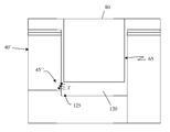
- FIG. 5 depicts etching an opening 75 in the BOX layer 35 ′ through the trench 65 to form an undercut 80 under a corner 45 ′ of the SOI island 40 ′.
- the etch process is selective to the material of the liner 70 , the material of the semiconductor layer 37 , and the material of the capacitor 50 , such that the etch process removes material of the BOX layer 35 ′ without removing substantially any material from the liner 70 , the semiconductor layer 37 , or the capacitor 50 .
- the etch process is isotropic so that it travels laterally from the bottom of the trench 65 to underneath the corner 45 ′ of the SOI island 40 ′.
- the etch process may comprise an oxide chemical etch that is isotropic and is highly selective of the BOX layer 35 ′ relative to the nitride liner 70 and the silicon semiconductor layer 37 ; however, any suitable etch process may be used within the scope of the invention.
- the opening 75 in the BOX layer 35 ′ has a depth “D” of about 5 nm to about 10 nm, and the undercut 80 extends laterally underneath the corner 45 ′ of the SOI island 40 ′ by a dimension “d” of about 5 nm.
- the invention is not limited to these particular values for dimensions “D” and “d”; however, and any suitable values may be used within the scope of the invention.
- the dimensions “D” and “d” may be controlled by controlling the timing of the etch process of the BOX layer 35 ′.
- a source doping layer 100 is formed in the opening 75 in the BOX layer 35 ′.
- the material of the source doping layer 100 fills the opening 75 and contacts the underside of the corner 45 ′ of the SOI island 40 ′.
- the source doping layer 100 may extend upward out of the opening 75 , and may even be formed on the liner 70 and the pad nitride 60 ; however, such coverage is optional.
- the source doping layer 100 is composed of a material comprising a p-type dopant, such as boron or any other suitable p-type dopant.
- the source doping layer 100 may be composed of boron silicide, borosilicate glass (BSG), boron doped polysilicon, or other suitable materials.
- BSG borosilicate glass
- boron doped polysilicon or other suitable materials.
- any suitable dopant, such as n-type dopants may be used based on the desired application, e.g., based on the desired intended use of the structure being fabricated.
- the concentration of dopant in the source doping layer 100 is about 3e20 atoms/cm 3 ; however, the invention is not limited to this concentration, and any suitable concentration may be used within the scope of the invention.
- the source doping layer 100 may be formed using conventional fabrication processes, such as, but not limited to: ALD, MLD, CVD, LPCVD, PECVD, etc.
- an thermal anneal process is performed to drive the dopant from the source doping layer 100 into the corner 45 ′ of the SOI island 40 ′.
- the anneal process is a rapid thermal anneal (RTA) that is performed at about 1000° C. for about 5 seconds; however, the invention is not limited to these anneal parameters, and any suitable annealing may be performed.
- the anneal causes at least a portion of the p-type dopant ions that are present in the source doping layer 100 to migrate into the corner 45 ′ of the SOI island 40 ′ as represented by arrows “I” in FIG. 6 .
- FIG. 7 shows simulation results of dopant density at the corner 45 ′ of the SOI island 40 ′.
- FIG. 7 depicts the doping distribution at the end of front end of line (FEOL) processes, which may include the RTA described above and other thermal steps.
- the doping of the corner 45 ′ results in a doped area that extends a distance “dp” up the sidewall of the SOI island 40 ′ from the bottom of the corner 45 ′ and about the same distance “dp” along the bottom of the SOI island 40 ′ from the apex of the corner 45 ′.
- the distance “dp” is about 5 nm and the doped area has a concentration of about 1e18 atoms/cm 3 .
- the spatial extent and concentration of the doping in the corner 45 ′ are not limited to these particular values, and any suitable doping of the corner 45 ′ may be performed. It is noted, however, that the doping is confined to the corner 45 ′ and does not extend into the remainder of the SOI island 40 ′ and process parameters should be tailored to provide these characteristics.
- the doping extends along less than one-third the length of the side and bottom surfaces of the SOI island 40 ′.
- implementations of the invention provide the ability to dope only the corner region of the SOI island 40 ′, without doping regions of the SOI island 40 ′ beyond the corner.
- the doping is said to be tailored and localized to the corner region of the SOI island. That is, implementations of the invention avoid doping the entire sidewall and/or the entire bottom surface of the SOI island 40 ′. This selective doping confines the dopant to the corner 45 ′ and avoids negative effects that may occur as a result of over-doping the SOI island 40 ′.
- implementations of the invention provide for tailoring a localized doping of the corner region 45 ′, and this tailored doping produces the effect of reducing or preventing capacitive coupling between the SOI island 40 ′ and an adjacent structure such as the capacitor 50 .
- FIG. 8 shows the structure after doping the corner, removing the source doping layer 100 , and filling the trench 65 with isolation material 80 .
- the source doping layer 100 is removed from the opening 75 and the trench 65 using a chemical etch that has a high selectivity of the material of the source doping layer 100 relative to the surrounding materials.
- the source doping layer 100 may be composed of 5% BSG, which may have an etch ratio of about 50:1 relative to oxide.
- the opening 75 and trench 65 are filled with isolation material 80 , such as SiO 2 , using conventional techniques, such as thermal oxidation, chemical oxidation, ALD, MLD, CVD, LPCVD, PECVD, etc.
- the liner 70 may or may not be removed or thinned using a reactive ion etch (RIE) process prior to filling the trench 65 .
- RIE reactive ion etch
- conventional processing steps may be performed. For example, an STI anneal may be performed, one or more FETs may be formed in the SOI island 40 ′, wiring and interconnects may be formed, etc.
- the corner 45 ′ may be doped using a gas phase doping process.
- a process gas containing boron may be introduced at a predetermined pressure inside a vacuum chamber while heating the wafer, including SOI island 40 ′ and corner 45 ′, to a temperature higher than 600° C.
- the process gas can be pyrolyzed to allow direct reaction of boron atoms or molecules containing boron with silicon atoms of the SOI island 40 ′ to thereby form a boron-silicon compound at the corner 45 ′.
- the exposed corner 45 ′ can be doped with boron; however, the remainder of the SOI island 40 ′ is not doped since it is covered and therefore not exposed to the process gas.
- the trench 65 may be formed between an SOI island 40 ′ and a deep trench capacitor 50 .
- FIG. 9 shows an alternative embodiment in which the STI trench 65 is formed between two SOI islands 40 ′, rather than between one STI island 40 ′ and a deep trench capacitor 50 as depicted in FIGS. 4-8 .
- the opening 75 formed in the BOX layer 35 ′ extends under both SOI islands 40 ′, such that a respective undercut 80 is formed under a respective corner 45 ′ of each of the SOI islands 40 ′.
- the respective corners 45 ′ of two adjacent SOI islands 40 ′ may be doped through a single trench 65 using a doping source layer (as described above with respect to FIG. 6 ) or by gas phase doping (as described above).
- an exemplary embodiment includes forming the trench 65 , forming a layer of material in the trench 65 , doping the layer of material, filling the trench with STI material, and using subsequent annealing steps to drive the dopant from the doped layer in the trench into the corner of the SOI island.
- FIG. 10 shows a wafer comprising a BOX layer 35 ′, a semiconductor layer 37 ′, a layer of pad oxide 55 , a layer of pad nitride 60 , a deep trench capacitor 50 , and a trench 65 .
- the features of the wafer in FIG. 10 may be similar to, and formed in a similar manner as, those described above with respect to FIGS. 3 and 4 .
- the trench 65 extends to the upper surface of the BOX layer 35 ′ or may optionally be over-etched into the BOX layer 35 ′.
- a layer of insulating material 120 is formed at the base of the trench 65 and in contact with the corner 45 ′ of the SOI island 40 ′.
- the layer of insulating material 120 does not fill the trench 65 , but rather only extends upward a height “H” above the interface between the BOX layer 35 ′ and the SOI island 40 ′. In this manner, a portion of the layer of insulating material 120 directly contacts the corner 45 ′ along the height “H”.
- the height “H” is about 5 nm and corresponds to an extent of doping that will be applied to the corner 45 ′ of the SOI island 40 ′.
- a liner 70 is formed on the sidewalls of the trench 65 .
- the liner 70 may be formed in the same process as the layer of insulating material 120 , or may be formed in a different step.
- the liner 70 may be composed of a same material as the layer of insulating material 120 , or may be composed of a different material.
- both the liner 70 and the layer of insulating material 120 are composed of oxide, such as SiO 2 , and are formed using suitable techniques such as thermal oxidation, chemical oxidation, ALD, MLD, CVD, LPCVD, PECVD, etc.; however, the invention is not limited to these materials, and any suitable STI materials may be used within the scope of the invention.
- the liner 70 and layer of insulating material 120 do not fill the trench 65 .
- a dopant is implanted into the layer of insulating material 120 .
- the dopant is a p-type dopant such as boron; however, any suitable p-type dopant may be used.
- the doping of the layer of insulating material 120 is performed with a substantially vertical implant at an energy of about 0.7 keV, although any desired implant angle and energy may be used. The angle and energy of the implant cause the implanted ions to scatter laterally within the layer of insulating material 120 , which results in the corner 125 of the layer of insulating material 120 having a much higher concentration of dopant than the liner 70 .
- the trench 65 is filled with an isolation material 80 , which may include forming oxide such as SiO 2 in the trench using methods such as thermal oxidation, chemical oxidation, ALD, MLD, CVD, LPCVD, PECVD, etc.
- an isolation material 80 may include forming oxide such as SiO 2 in the trench using methods such as thermal oxidation, chemical oxidation, ALD, MLD, CVD, LPCVD, PECVD, etc.
- chip fabrication may continue with known processes, such as an STI anneal, FET formation, silicide formation, forming wiring and interconnects, etc.
- thermal annealing steps involved in the subsequent processing steps drive the dopant from the corner 125 of the layer of insulating material 120 into the corner 45 ′ of the SOI island 40 ′.
- thermal annealing steps involved in the subsequent processing steps drive the dopant from the corner 125 of the layer of insulating material 120 into the corner 45 ′ of the SOI island 40 ′.
- the elevated temperature of the STI anneal causes at least a portion of the p-type ions to migrate from the corner 125 of the layer of insulating material 120 into the corner 45 ′ of the SOI island 40 ′, as depicted by arrows I′.
- the elevated temperature of the silicide anneal causes the p-type ions to migrate from the corner 125 of the layer of insulating material 120 into the corner 45 ′ of the SOI island 40 ′. Accordingly, in the embodiments shown in FIGS. 10-13 , the doping of the corner 45 ′ of the SOI island 40 ′ occurs after the trench 65 is filled. Moreover, in the embodiment show in FIGS. 10-13 , it is not necessary to perform an additional etch of the BOX layer to form undercuts under the SOI island.
- FIG. 14 shows simulation results of dopant density after the trench 65 is filled and a subsequent anneal process drives the dopant into the corner 45 ′ of the SOI island 40 ′.
- the doping of the corner 45 ′ results in a doped area that extends a distance “dpp” up the sidewall of the SOI island 40 ′ from the vertex of the corner 45 ′ and about the same distance “dpp” along the bottom surface of the SOI island 40 ′ from the vertex of the corner 45 ′.
- the distance “dpp” is about 5 nm and the doped area has a concentration of about 1e18 atoms/cm 3 .
- the spatial extent and concentration of the doping in the corner 45 ′ are not limited to these particular values, and any suitable doping of the corner 45 ′ may be performed to provide tailored doping characteristics. It is noted, however, that the doping is confined to the corner 45 ′ and does not extend into the remainder of the SOI island 40 ′. This is due to the relatively high concentration of dopant in the corner 125 of the layer of insulating material 120 that contacts the corner 45 ′ of the SOI island 40 ′, and the relatively low concentration of dopant in the liner 70 .
- FIG. 14 depicts that a relatively low concentration of doping may occur along the length of the sidewall of the SOI island 40 ′.
- the doping concentration is significantly lower than the doping concentration in the region of the corner 45 .
- the doping concentration at the corner 45 ′ is at least one full order of magnitude greater than the doping concentration at other locations 200 along the sidewall and locations 205 along the bottom surface of the SOI island 40 ′.
- the doping is said to be tailored and localized to the corner region of the SOI island.
- implementations of the invention provide a tailored and localized doping of the corner region 45 ′, and this tailored doping produces the effect of reducing or preventing capacitive coupling between the SOI island 40 ′ and an adjacent structure such as the capacitor 50 .
- FIG. 15 is a flow diagram of a design process used in semiconductor design, manufacture, and/or test.
- FIG. 15 shows a block diagram of an exemplary design flow 900 used for example, in semiconductor IC logic design, simulation, test, layout, and manufacture.
- Design flow 900 includes processes, machines and/or mechanisms for processing design structures or devices to generate logically or otherwise functionally equivalent representations of the design structures and/or devices described above and shown in FIGS. 1-6 and 8-13 .
- the design structures processed and/or generated by design flow 900 may be encoded on machine-readable transmission or storage media to include data and/or instructions that when executed or otherwise processed on a data processing system generate a logically, structurally, mechanically, or otherwise functionally equivalent representation of hardware components, circuits, devices, or systems.
- Machines include, but are not limited to, any machine used in an IC design process, such as designing, manufacturing, or simulating a circuit, component, device, or system.
- machines may include: lithography machines, machines and/or equipment for generating masks (e.g. e-beam writers), computers or equipment for simulating design structures, any apparatus used in the manufacturing or test process, or any machines for programming functionally equivalent representations of the design structures into any medium (e.g. a machine for programming a programmable gate array).
- Design flow 900 may vary depending on the type of representation being designed. For example, a design flow 900 for building an application specific IC (ASIC) may differ from a design flow 900 for designing a standard component or from a design flow 900 for instantiating the design into a programmable array, for example a programmable gate array (PGA) or a field programmable gate array (FPGA) offered by Altera® Inc. or Xilinx® Inc.
- ASIC application specific IC
- PGA programmable gate array
- FPGA field programmable gate array
- FIG. 15 illustrates multiple such design structures including an input design structure 920 that is preferably processed by a design process 910 .
- Design structure 920 may be a logical simulation design structure generated and processed by design process 910 to produce a logically equivalent functional representation of a hardware device.
- Design structure 920 may also or alternatively comprise data and/or program instructions that when processed by design process 910 , generate a functional representation of the physical structure of a hardware device. Whether representing functional and/or structural design features, design structure 920 may be generated using electronic computer-aided design (ECAD) such as implemented by a core developer/designer.
- ECAD electronic computer-aided design
- design structure 920 When encoded on a machine-readable data transmission, gate array, or storage medium, design structure 920 may be accessed and processed by one or more hardware and/or software modules within design process 910 to simulate or otherwise functionally represent an electronic component, circuit, electronic or logic module, apparatus, device, or system such as those shown in FIGS. 1-6 and 8-13 .
- design structure 920 may comprise files or other data structures including human and/or machine-readable source code, compiled structures, and computer-executable code structures that when processed by a design or simulation data processing system, functionally simulate or otherwise represent circuits or other levels of hardware logic design.
- Such data structures may include hardware-description language (HDL) design entities or other data structures conforming to and/or compatible with lower-level HDL design languages such as Verilog and VHDL, and/or higher level design languages such as C or C++.
- HDL hardware-description language
- Design process 910 preferably employs and incorporates hardware and/or software modules for synthesizing, translating, or otherwise processing a design/simulation functional equivalent of the components, circuits, devices, or logic structures shown in FIGS. 1-6 and 8-13 to generate a netlist 980 which may contain design structures such as design structure 920 .
- Netlist 980 may comprise, for example, compiled or otherwise processed data structures representing a list of wires, discrete components, logic gates, control circuits, I/O devices, models, etc. that describes the connections to other elements and circuits in an integrated circuit design.
- Netlist 980 may be synthesized using an iterative process in which netlist 980 is resynthesized one or more times depending on design specifications and parameters for the device.
- netlist 980 may be recorded on a machine-readable data storage medium or programmed into a programmable gate array.
- the medium may be a non-volatile storage medium such as a magnetic or optical disk drive, a programmable gate array, a compact flash, or other flash memory. Additionally, or in the alternative, the medium may be a system or cache memory, buffer space, or electrically or optically conductive devices and materials on which data packets may be transmitted and intermediately stored via the Internet, or other networking suitable means.
- Design process 910 may include hardware and software modules for processing a variety of input data structure types including netlist 980 .
- data structure types may reside, for example, within library elements 930 and include a set of commonly used elements, circuits, and devices, including models, layouts, and symbolic representations, for a given manufacturing technology (e.g., different technology nodes, 32 nm, 45 nm, 90 nm, etc.).
- the data structure types may further include design specifications 940 , characterization data 950 , verification data 960 , design rules 970 , and test data files 985 which may include input test patterns, output test results, and other testing information.
- Design process 910 may further include, for example, standard mechanical design processes such as stress analysis, thermal analysis, mechanical event simulation, process simulation for operations such as casting, molding, and die press forming, etc.
- standard mechanical design processes such as stress analysis, thermal analysis, mechanical event simulation, process simulation for operations such as casting, molding, and die press forming, etc.
- One of ordinary skill in the art of mechanical design can appreciate the extent of possible mechanical design tools and applications used in design process 910 without deviating from the scope and spirit of the invention.
- Design process 910 may also include modules for performing standard circuit design processes such as timing analysis, verification, design rule checking, place and route operations, etc.
- Design process 910 employs and incorporates logic and physical design tools such as HDL compilers and simulation model build tools to process design structure 920 together with some or all of the depicted supporting data structures along with any additional mechanical design or data (if applicable), to generate a second design structure 990 .
- logic and physical design tools such as HDL compilers and simulation model build tools
- Design structure 990 resides on a storage medium or programmable gate array in a data format used for the exchange of data of mechanical devices and structures (e.g. information stored in a IGES, DXF, Parasolid XT, JT, DRG, or any other suitable format for storing or rendering such mechanical design structures). Similar to design structure 920 , design structure 990 preferably comprises one or more files, data structures, or other computer-encoded data or instructions that reside on transmission or data storage media and that when processed by an ECAD system generate a logically or otherwise functionally equivalent form of one or more of the embodiments of the invention shown in FIGS. 1-6 and 8-13 . In one embodiment, design structure 990 may comprise a compiled, executable HDL simulation model that functionally simulates the devices shown in FIGS. 1-6 and 8-13 .
- Design structure 990 may also employ a data format used for the exchange of layout data of integrated circuits and/or symbolic data format (e.g. information stored in a GDSII (GDS2), GL1, OASIS, map files, or any other suitable format for storing such design data structures).
- Design structure 990 may comprise information such as, for example, symbolic data, map files, test data files, design content files, manufacturing data, layout parameters, wires, levels of metal, vias, shapes, data for routing through the manufacturing line, and any other data required by a manufacturer or other designer/developer to produce a device or structure as described above and shown in FIGS. 1-6 and 8-13 .
- Design structure 990 may then proceed to a stage 995 where, for example, design structure 990 : proceeds to tape-out, is released to manufacturing, is released to a mask house, is sent to another design house, is sent back to the customer, etc.
- the method as described above is used in the fabrication of integrated circuit chips.
- the resulting integrated circuit chips can be distributed by the fabricator in raw wafer form (that is, as a single wafer that has multiple unpackaged chips), as a bare die, or in a packaged form.
- the chip is mounted in a single chip package (such as a plastic carrier, with leads that are affixed to a motherboard or other higher level carrier) or in a multichip package (such as a ceramic carrier that has either or both surface interconnections or buried interconnections).
- the chip is then integrated with other chips, discrete circuit elements, and/or other signal processing devices as part of either (a) an intermediate product, such as a motherboard, or (b) an end product.
- the end product can be any product that includes integrated circuit chips, ranging from toys and other low-end applications to advanced computer products having a display, a keyboard or other input device, and a central processor.
Abstract
Description
Claims (6)
Priority Applications (1)
| Application Number | Priority Date | Filing Date | Title |
|---|---|---|---|
| US12/822,492 US9484269B2 (en) | 2010-06-24 | 2010-06-24 | Structure and method to control bottom corner threshold in an SOI device |
Applications Claiming Priority (1)
| Application Number | Priority Date | Filing Date | Title |
|---|---|---|---|
| US12/822,492 US9484269B2 (en) | 2010-06-24 | 2010-06-24 | Structure and method to control bottom corner threshold in an SOI device |
Publications (2)
| Publication Number | Publication Date |
|---|---|
| US20110316061A1 US20110316061A1 (en) | 2011-12-29 |
| US9484269B2 true US9484269B2 (en) | 2016-11-01 |
Family
ID=45351710
Family Applications (1)
| Application Number | Title | Priority Date | Filing Date |
|---|---|---|---|
| US12/822,492 Active 2032-12-08 US9484269B2 (en) | 2010-06-24 | 2010-06-24 | Structure and method to control bottom corner threshold in an SOI device |
Country Status (1)
| Country | Link |
|---|---|
| US (1) | US9484269B2 (en) |
Citations (34)
| Publication number | Priority date | Publication date | Assignee | Title |
|---|---|---|---|---|
| US4999312A (en) * | 1988-08-18 | 1991-03-12 | Hyundai Electronics Industries Co., Ltd. | Doping method using an oxide film and a nitride film on the trench wall to manufacture a semiconductor device and the manufactured device |
| US5053345A (en) | 1989-02-06 | 1991-10-01 | Harris Corporation | Method of edge doping SOI islands |
| US5346839A (en) | 1991-06-10 | 1994-09-13 | Texas Instruments Incorporated | Sidewall doping technique for SOI transistors |
| US5753530A (en) | 1992-04-21 | 1998-05-19 | Seiko Instruments, Inc. | Impurity doping method with diffusion source of boron-silicide film |
| US5953607A (en) * | 1997-06-06 | 1999-09-14 | International Business Machines Corporation | Buried strap for trench storage capacitors in dram trench cells |
| US6323082B1 (en) * | 1998-07-30 | 2001-11-27 | International Business Machines Corporation | Process for making a DRAM cell with three-sided gate transfer |
| US6344390B1 (en) * | 1999-07-01 | 2002-02-05 | International Business Machines Corporation | Methods of forming the buried strap and its quantum barrier in deep trench cell capacitors |
| US20020022326A1 (en) * | 1999-11-11 | 2002-02-21 | Mitsubishi Denki Kabushiki Kaisha | Semiconductor device and method of manufacturing the same |
| US6426252B1 (en) * | 1999-10-25 | 2002-07-30 | International Business Machines Corporation | Silicon-on-insulator vertical array DRAM cell with self-aligned buried strap |
| US6486024B1 (en) * | 2000-05-24 | 2002-11-26 | Infineon Technologies Ag | Integrated circuit trench device with a dielectric collar stack, and method of forming thereof |
| US20020179997A1 (en) | 2001-06-05 | 2002-12-05 | International Business Machines Corporation | Self-aligned corner Vt enhancement with isolation channel stop by ion implantation |
| US20030013259A1 (en) * | 2001-07-13 | 2003-01-16 | International Business Machines Corporation | Reduction of polysilicon stress in trench capacitors |
| US6566177B1 (en) * | 1999-10-25 | 2003-05-20 | International Business Machines Corporation | Silicon-on-insulator vertical array device trench capacitor DRAM |
| US6579759B1 (en) * | 2002-08-23 | 2003-06-17 | International Business Machines Corporation | Formation of self-aligned buried strap connector |
| US20030168687A1 (en) * | 2002-03-11 | 2003-09-11 | International Business Machines Corporation | Vertical MOSFET with horizontally graded channel doping |
| US6638815B1 (en) * | 2002-10-25 | 2003-10-28 | International Business Machines Corporation | Formation of self-aligned vertical connector |
| US20030203587A1 (en) * | 2001-12-10 | 2003-10-30 | Oleg Gluschenkov | Vertical thermal nitride mask (anti-collar) and processing thereof |
| US6762099B1 (en) * | 2003-07-01 | 2004-07-13 | Nanya Technology Corp. | Method for fabricating buried strap out-diffusions of vertical transistor |
| US20050009268A1 (en) * | 2003-06-25 | 2005-01-13 | International Business Machines Corporation | Method for forming buried plate of trench capacitor |
| US20050037566A1 (en) * | 2003-08-12 | 2005-02-17 | Tzu-Ching Tsai | [split gate flash memory cell and manufacturing method thereof] |
| US20050059207A1 (en) * | 2003-09-17 | 2005-03-17 | Chih-Han Chang | Method for forming a deep trench capacitor buried plate |
| US20060175660A1 (en) * | 2005-02-10 | 2006-08-10 | International Business Machines Corporation | Vertical body-contacted soi transistor |
| US20060267134A1 (en) | 2005-05-10 | 2006-11-30 | Armin Tilke | Deep trench isolation structures and methods of formation thereof |
| US20070054432A1 (en) * | 2005-08-22 | 2007-03-08 | Qimonda Ag | Method for producing a structure with a low aspect ratio |
| US7294543B2 (en) * | 2006-03-22 | 2007-11-13 | International Business Machines Corporation | DRAM (Dynamic Random Access Memory) cells |
| US20080124863A1 (en) * | 2006-01-06 | 2008-05-29 | Kangguo Cheng | Trench Memory |
| US7491995B2 (en) | 2006-04-04 | 2009-02-17 | Micron Technology, Inc. | DRAM with nanofin transistors |
| US20090173980A1 (en) * | 2008-01-07 | 2009-07-09 | International Business Machines Corporation | Providing isolation for wordline passing over deep trench capacitor |
| US7803701B2 (en) * | 2007-09-12 | 2010-09-28 | Nanya Technology Corporation | Method for fabricating a semiconductor device |
| US7898014B2 (en) * | 2006-03-30 | 2011-03-01 | International Business Machines Corporation | Semiconductor device structures with self-aligned doped regions and methods for forming such semiconductor device structures |
| US20110081757A1 (en) * | 2007-01-22 | 2011-04-07 | Werner Juengling | Memory having a vertical access device |
| US20110291169A1 (en) * | 2010-06-01 | 2011-12-01 | International Business Machines Corporation | Reduced corner leakage in soi structure and method |
| US20120104547A1 (en) * | 2010-11-01 | 2012-05-03 | International Business Machines Corporation | Lateral epitaxial grown soi in deep trench structures and methods of manufacture |
| US20120211814A1 (en) * | 2007-04-18 | 2012-08-23 | International Business Machines Corporation | trench structure and method of forming the trench structure |
-
2010
- 2010-06-24 US US12/822,492 patent/US9484269B2/en active Active
Patent Citations (40)
| Publication number | Priority date | Publication date | Assignee | Title |
|---|---|---|---|---|
| US4999312A (en) * | 1988-08-18 | 1991-03-12 | Hyundai Electronics Industries Co., Ltd. | Doping method using an oxide film and a nitride film on the trench wall to manufacture a semiconductor device and the manufactured device |
| US5053345A (en) | 1989-02-06 | 1991-10-01 | Harris Corporation | Method of edge doping SOI islands |
| US5346839A (en) | 1991-06-10 | 1994-09-13 | Texas Instruments Incorporated | Sidewall doping technique for SOI transistors |
| US5753530A (en) | 1992-04-21 | 1998-05-19 | Seiko Instruments, Inc. | Impurity doping method with diffusion source of boron-silicide film |
| US5953607A (en) * | 1997-06-06 | 1999-09-14 | International Business Machines Corporation | Buried strap for trench storage capacitors in dram trench cells |
| US6323082B1 (en) * | 1998-07-30 | 2001-11-27 | International Business Machines Corporation | Process for making a DRAM cell with three-sided gate transfer |
| US6344390B1 (en) * | 1999-07-01 | 2002-02-05 | International Business Machines Corporation | Methods of forming the buried strap and its quantum barrier in deep trench cell capacitors |
| US6566177B1 (en) * | 1999-10-25 | 2003-05-20 | International Business Machines Corporation | Silicon-on-insulator vertical array device trench capacitor DRAM |
| US6426252B1 (en) * | 1999-10-25 | 2002-07-30 | International Business Machines Corporation | Silicon-on-insulator vertical array DRAM cell with self-aligned buried strap |
| US20020022326A1 (en) * | 1999-11-11 | 2002-02-21 | Mitsubishi Denki Kabushiki Kaisha | Semiconductor device and method of manufacturing the same |
| US6486024B1 (en) * | 2000-05-24 | 2002-11-26 | Infineon Technologies Ag | Integrated circuit trench device with a dielectric collar stack, and method of forming thereof |
| US20020179997A1 (en) | 2001-06-05 | 2002-12-05 | International Business Machines Corporation | Self-aligned corner Vt enhancement with isolation channel stop by ion implantation |
| US20030013259A1 (en) * | 2001-07-13 | 2003-01-16 | International Business Machines Corporation | Reduction of polysilicon stress in trench capacitors |
| US20030203587A1 (en) * | 2001-12-10 | 2003-10-30 | Oleg Gluschenkov | Vertical thermal nitride mask (anti-collar) and processing thereof |
| US20030168687A1 (en) * | 2002-03-11 | 2003-09-11 | International Business Machines Corporation | Vertical MOSFET with horizontally graded channel doping |
| US6740920B2 (en) * | 2002-03-11 | 2004-05-25 | International Business Machines Corporation | Vertical MOSFET with horizontally graded channel doping |
| US6579759B1 (en) * | 2002-08-23 | 2003-06-17 | International Business Machines Corporation | Formation of self-aligned buried strap connector |
| US6638815B1 (en) * | 2002-10-25 | 2003-10-28 | International Business Machines Corporation | Formation of self-aligned vertical connector |
| US20050009268A1 (en) * | 2003-06-25 | 2005-01-13 | International Business Machines Corporation | Method for forming buried plate of trench capacitor |
| US6969648B2 (en) * | 2003-06-25 | 2005-11-29 | International Business Machines Corporation | Method for forming buried plate of trench capacitor |
| US6762099B1 (en) * | 2003-07-01 | 2004-07-13 | Nanya Technology Corp. | Method for fabricating buried strap out-diffusions of vertical transistor |
| US20050037566A1 (en) * | 2003-08-12 | 2005-02-17 | Tzu-Ching Tsai | [split gate flash memory cell and manufacturing method thereof] |
| US20050037567A1 (en) * | 2003-08-12 | 2005-02-17 | Tzu-Ching Tsai | [split gate flash memory cell and manufacturing method thereof] |
| US20050059207A1 (en) * | 2003-09-17 | 2005-03-17 | Chih-Han Chang | Method for forming a deep trench capacitor buried plate |
| US7232718B2 (en) * | 2003-09-17 | 2007-06-19 | Nanya Technology Corp. | Method for forming a deep trench capacitor buried plate |
| US20060175660A1 (en) * | 2005-02-10 | 2006-08-10 | International Business Machines Corporation | Vertical body-contacted soi transistor |
| US7759188B2 (en) * | 2005-02-10 | 2010-07-20 | International Business Machines Corporation | Method of fabricating vertical body-contacted SOI transistor |
| US20080102569A1 (en) * | 2005-02-10 | 2008-05-01 | Kangguo Cheng | Method of fabricating vertical body-contacted SOI transistor |
| US20060267134A1 (en) | 2005-05-10 | 2006-11-30 | Armin Tilke | Deep trench isolation structures and methods of formation thereof |
| US20070054432A1 (en) * | 2005-08-22 | 2007-03-08 | Qimonda Ag | Method for producing a structure with a low aspect ratio |
| US20080124863A1 (en) * | 2006-01-06 | 2008-05-29 | Kangguo Cheng | Trench Memory |
| US7294543B2 (en) * | 2006-03-22 | 2007-11-13 | International Business Machines Corporation | DRAM (Dynamic Random Access Memory) cells |
| US7898014B2 (en) * | 2006-03-30 | 2011-03-01 | International Business Machines Corporation | Semiconductor device structures with self-aligned doped regions and methods for forming such semiconductor device structures |
| US7491995B2 (en) | 2006-04-04 | 2009-02-17 | Micron Technology, Inc. | DRAM with nanofin transistors |
| US20110081757A1 (en) * | 2007-01-22 | 2011-04-07 | Werner Juengling | Memory having a vertical access device |
| US20120211814A1 (en) * | 2007-04-18 | 2012-08-23 | International Business Machines Corporation | trench structure and method of forming the trench structure |
| US7803701B2 (en) * | 2007-09-12 | 2010-09-28 | Nanya Technology Corporation | Method for fabricating a semiconductor device |
| US20090173980A1 (en) * | 2008-01-07 | 2009-07-09 | International Business Machines Corporation | Providing isolation for wordline passing over deep trench capacitor |
| US20110291169A1 (en) * | 2010-06-01 | 2011-12-01 | International Business Machines Corporation | Reduced corner leakage in soi structure and method |
| US20120104547A1 (en) * | 2010-11-01 | 2012-05-03 | International Business Machines Corporation | Lateral epitaxial grown soi in deep trench structures and methods of manufacture |
Also Published As
| Publication number | Publication date |
|---|---|
| US20110316061A1 (en) | 2011-12-29 |
Similar Documents
| Publication | Publication Date | Title |
|---|---|---|
| US10818668B2 (en) | Metal trench capacitor and improved isolation and methods of manufacture | |
| US8674472B2 (en) | Low harmonic RF switch in SOI | |
| US8963283B2 (en) | Method of fabricating isolated capacitors and structure thereof | |
| US10580686B2 (en) | Semiconductor structure with integrated passive structures | |
| US8470682B2 (en) | Methods and structures for increased thermal dissipation of thin film resistors | |
| US9240452B2 (en) | Array and moat isolation structures and method of manufacture | |
| US9171952B2 (en) | Low gate-to-drain capacitance fully merged finFET | |
| US9484269B2 (en) | Structure and method to control bottom corner threshold in an SOI device | |
| US9293593B2 (en) | Self aligned device with enhanced stress and methods of manufacture |
Legal Events
| Date | Code | Title | Description |
|---|---|---|---|
| AS | Assignment |
Owner name: INTERNATIONAL BUSINESS MACHINES CORPORATION, NEW Y Free format text: ASSIGNMENT OF ASSIGNORS INTEREST;ASSIGNORS:ERVIN, JOSEPH;JOHNSON, JEFFREY B.;MCSTAY, KEVIN;AND OTHERS;SIGNING DATES FROM 20100621 TO 20100622;REEL/FRAME:024589/0562 |
|
| AS | Assignment |
Owner name: GLOBALFOUNDRIES U.S. 2 LLC, NEW YORK Free format text: ASSIGNMENT OF ASSIGNORS INTEREST;ASSIGNOR:INTERNATIONAL BUSINESS MACHINES CORPORATION;REEL/FRAME:036550/0001 Effective date: 20150629 |
|
| AS | Assignment |
Owner name: GLOBALFOUNDRIES INC., CAYMAN ISLANDS Free format text: ASSIGNMENT OF ASSIGNORS INTEREST;ASSIGNORS:GLOBALFOUNDRIES U.S. 2 LLC;GLOBALFOUNDRIES U.S. INC.;REEL/FRAME:036779/0001 Effective date: 20150910 |
|
| STCF | Information on status: patent grant |
Free format text: PATENTED CASE |
|
| AS | Assignment |
Owner name: WILMINGTON TRUST, NATIONAL ASSOCIATION, DELAWARE Free format text: SECURITY AGREEMENT;ASSIGNOR:GLOBALFOUNDRIES INC.;REEL/FRAME:049490/0001 Effective date: 20181127 |
|
| MAFP | Maintenance fee payment |
Free format text: PAYMENT OF MAINTENANCE FEE, 4TH YEAR, LARGE ENTITY (ORIGINAL EVENT CODE: M1551); ENTITY STATUS OF PATENT OWNER: LARGE ENTITY Year of fee payment: 4 |
|
| AS | Assignment |
Owner name: GLOBALFOUNDRIES U.S. INC., CALIFORNIA Free format text: ASSIGNMENT OF ASSIGNORS INTEREST;ASSIGNOR:GLOBALFOUNDRIES INC.;REEL/FRAME:054633/0001 Effective date: 20201022 |
|
| AS | Assignment |
Owner name: GLOBALFOUNDRIES INC., CAYMAN ISLANDS Free format text: RELEASE BY SECURED PARTY;ASSIGNOR:WILMINGTON TRUST, NATIONAL ASSOCIATION;REEL/FRAME:054636/0001 Effective date: 20201117 |
|
| AS | Assignment |
Owner name: GLOBALFOUNDRIES U.S. INC., NEW YORK Free format text: RELEASE BY SECURED PARTY;ASSIGNOR:WILMINGTON TRUST, NATIONAL ASSOCIATION;REEL/FRAME:056987/0001 Effective date: 20201117 |