US9504115B2 - Light source circuitry for controlling the color of emitted light - Google Patents

Light source circuitry for controlling the color of emitted light Download PDF

Info

Publication number
US9504115B2
US9504115B2 US14/400,088 US201314400088A US9504115B2 US 9504115 B2 US9504115 B2 US 9504115B2 US 201314400088 A US201314400088 A US 201314400088A US 9504115 B2 US9504115 B2 US 9504115B2
Authority
US
United States
Prior art keywords
emitting diodes
light emitting
group
transistor
circuitry
Prior art date
Legal status (The legal status is an assumption and is not a legal conclusion. Google has not performed a legal analysis and makes no representation as to the accuracy of the status listed.)
Active
Application number
US14/400,088
Other versions
US20150108919A1 (en
Inventor
Josephus Adrianus Maria Van Erp
Current Assignee (The listed assignees may be inaccurate. Google has not performed a legal analysis and makes no representation or warranty as to the accuracy of the list.)
Signify Holding BV
Original Assignee
Koninklijke Philips Electronics NV
Priority date (The priority date is an assumption and is not a legal conclusion. Google has not performed a legal analysis and makes no representation as to the accuracy of the date listed.)
Filing date
Publication date
Application filed by Koninklijke Philips Electronics NV filed Critical Koninklijke Philips Electronics NV
Priority to US14/400,088 priority Critical patent/US9504115B2/en
Assigned to KONINKLIJKE PHILIPS ELECTRONICS N.V. reassignment KONINKLIJKE PHILIPS ELECTRONICS N.V. ASSIGNMENT OF ASSIGNORS INTEREST (SEE DOCUMENT FOR DETAILS). Assignors: VAN ERP, JOSEPHUS ADRIANUS MARIA
Publication of US20150108919A1 publication Critical patent/US20150108919A1/en
Assigned to PHILIPS LIGHTING HOLDING B.V. reassignment PHILIPS LIGHTING HOLDING B.V. ASSIGNMENT OF ASSIGNORS INTEREST (SEE DOCUMENT FOR DETAILS). Assignors: KONINKLIJKE PHILIPS N.V.
Application granted granted Critical
Publication of US9504115B2 publication Critical patent/US9504115B2/en
Assigned to SIGNIFY HOLDING B.V. reassignment SIGNIFY HOLDING B.V. CHANGE OF NAME (SEE DOCUMENT FOR DETAILS). Assignors: PHILIPS LIGHTING HOLDING B.V.
Active legal-status Critical Current
Anticipated expiration legal-status Critical

Links

Images

Classifications

    • HELECTRICITY
    • H05ELECTRIC TECHNIQUES NOT OTHERWISE PROVIDED FOR
    • H05BELECTRIC HEATING; ELECTRIC LIGHT SOURCES NOT OTHERWISE PROVIDED FOR; CIRCUIT ARRANGEMENTS FOR ELECTRIC LIGHT SOURCES, IN GENERAL
    • H05B45/00Circuit arrangements for operating light-emitting diodes [LED]
    • H05B45/30Driver circuits
    • H05B45/395Linear regulators
    • H05B33/0857
    • H05B33/0812
    • H05B33/0827
    • HELECTRICITY
    • H05ELECTRIC TECHNIQUES NOT OTHERWISE PROVIDED FOR
    • H05BELECTRIC HEATING; ELECTRIC LIGHT SOURCES NOT OTHERWISE PROVIDED FOR; CIRCUIT ARRANGEMENTS FOR ELECTRIC LIGHT SOURCES, IN GENERAL
    • H05B45/00Circuit arrangements for operating light-emitting diodes [LED]
    • H05B45/20Controlling the colour of the light
    • HELECTRICITY
    • H05ELECTRIC TECHNIQUES NOT OTHERWISE PROVIDED FOR
    • H05BELECTRIC HEATING; ELECTRIC LIGHT SOURCES NOT OTHERWISE PROVIDED FOR; CIRCUIT ARRANGEMENTS FOR ELECTRIC LIGHT SOURCES, IN GENERAL
    • H05B45/00Circuit arrangements for operating light-emitting diodes [LED]
    • H05B45/40Details of LED load circuits
    • H05B45/44Details of LED load circuits with an active control inside an LED matrix
    • H05B45/46Details of LED load circuits with an active control inside an LED matrix having LEDs disposed in parallel lines
    • HELECTRICITY
    • H05ELECTRIC TECHNIQUES NOT OTHERWISE PROVIDED FOR
    • H05BELECTRIC HEATING; ELECTRIC LIGHT SOURCES NOT OTHERWISE PROVIDED FOR; CIRCUIT ARRANGEMENTS FOR ELECTRIC LIGHT SOURCES, IN GENERAL
    • H05B47/00Circuit arrangements for operating light sources in general, i.e. where the type of light source is not relevant
    • H05B47/20Responsive to malfunctions or to light source life; for protection
    • H05B47/25Circuit arrangements for protecting against overcurrent
    • YGENERAL TAGGING OF NEW TECHNOLOGICAL DEVELOPMENTS; GENERAL TAGGING OF CROSS-SECTIONAL TECHNOLOGIES SPANNING OVER SEVERAL SECTIONS OF THE IPC; TECHNICAL SUBJECTS COVERED BY FORMER USPC CROSS-REFERENCE ART COLLECTIONS [XRACs] AND DIGESTS
    • Y02TECHNOLOGIES OR APPLICATIONS FOR MITIGATION OR ADAPTATION AGAINST CLIMATE CHANGE
    • Y02BCLIMATE CHANGE MITIGATION TECHNOLOGIES RELATED TO BUILDINGS, e.g. HOUSING, HOUSE APPLIANCES OR RELATED END-USER APPLICATIONS
    • Y02B20/00Energy efficient lighting technologies, e.g. halogen lamps or gas discharge lamps
    • Y02B20/30Semiconductor lamps, e.g. solid state lamps [SSL] light emitting diodes [LED] or organic LED [OLED]
    • Y02B20/343
    • Y02B20/345

Definitions

  • the invention relates to light source circuitry and particularly to light source circuitry comprising light emitting diodes.
  • LEDs light emitting diodes
  • LEDs Due to their high luminous efficacy, light emitting diodes (LEDs) are being used in an ever-increasing range of lighting applications. LEDs provide a great number of different functionalities that are not possible, or are not as easy to achieve, with conventional light bulbs.
  • One such functionality is the ability to change the tint or color of a single light bulb.
  • PWM pulse width modulation
  • the use of PWM requires a power supply and circuitry that is able to cope with changing power levels and with high frequencies. This increases the monetary cost of the circuitry and can also adversely affect its electro-magnetic capability (EMC).
  • EMC electro-magnetic capability
  • the present invention provides light source circuitry comprising a first group of one or more light emitting diodes operable to emit light of a first color, a second group of one or more light emitting diodes operable to emit light of a second color, and a third group of one or more light emitting diodes operable to emit light of a third color.
  • the first, second and third groups of light emitting diodes are arranged such that, when a fixed current arrives at the light source circuitry, the fixed current is shared between the first, second and third groups.
  • the circuitry is configured such that a proportion of the fixed current that flows through each of the first and second groups is controllable in dependence on a received control signal and such that the remainder of the fixed current flows through the third group.
  • the combined emissions of the light source circuitry can be gradually varied over a range of chromaticities, using only a single control signal.
  • changing the chromaticity of the combined emission is relatively straightforward and can be carried out using existing infrastructure, such as conventional dimmer switches regulating a mains power supply.
  • changing the chromaticity does not require the use of PWM and so the PWM-specific requirements on the power are not necessary. Consequently, the power supply to the circuitry can be simpler.
  • Many existing power supplies for conventional LED bulbs are configured so as to provide a constant current. As such, the light source circuitry according to the invention can be easily utilized with existing power supplies.
  • the light source circuitry may further comprise a first transistor connected in series with the first group of light emitting diodes, a second transistor connected in series with the second group of light emitting diodes, wherein the circuitry is configured such that a variation in the control signal causes a variation in the proportion of the fixed current that flows through the first transistor and second transistor.
  • the circuitry may be configured such that a first signal based on the control signal is provided to the control terminal of the first transistor and such that a second signal based on the control signal is provided to the control terminal of the second transistor.
  • the light source circuitry may be configured such that the first and second signals based on the control signal vary relative to one another in dependence on the control signal.
  • the light source circuitry may further comprise a third transistor connected in series with the third group of light emitting diodes. A third signal based on the control signal may be received at the control terminal of the third transistor, wherein the third signal is always larger than the first and second signals.
  • the combined forward voltage of the third group of light emitting diodes may be larger than the combined forward voltage of the first group of light emitting diodes and the combined forward voltage of the second group of light emitting diodes.
  • the light source circuitry may be configured such that when the control signal is at a first level, the largest proportion of the fixed current flows through the third group of light emitting diodes and such that, as the control signal changes to second level, the proportions of the fixed current that flow through the first and second groups of light emitting diodes increase.
  • the circuitry may be configured such that, as the control signal changes from the second level to a third level, the proportion of the fixed current that flows in the first group of light emitting diodes decreases, and the proportion of the fixed current that flows in the second group of light emitting diodes continues to increase.
  • the second group of light emitting diodes may be constituted by one or more light emitting diodes operable to emit red-colored light
  • the third group of light emitting diodes may be constituted by one or more light emitting diodes operable to emit white-colored light
  • the first group of light emitting diodes may be constituted by one or more light emitting diodes the combined emission of which is lime-colored.
  • the light source circuitry may be configured such that, as the control signal gradually changes from a first level to a different level, the color of the combined emissions of the first, second and third groups of light emitting diodes changes generally in accordance with the Planckian locus.
  • the Planckian locus is the representation of different tints of white that are available using various different technologies. Colors falling on the Planckian locus are perceived by consumers to be white, but having different “warmths”.
  • the light source circuitry can be used to provide subtle changes in atmosphere by varying the warmth of the emitted light. Changing the color of light along the Planckian locus can influence people's moods and their perception of the ambient atmosphere. In contrast, when deviating from the Planckian locus, people may perceive the light to be colored instead of white, and so the above advantages may not apply.
  • the present invention provides a method of manufacturing light source circuitry comprising providing a first group of one or more light emitting diodes operable to emit light of a first color, providing a second group of one or more light emitting diodes operable to emit light of a second color, providing a third group of one or more light emitting diodes operable to emit light of third color, arranging the first, second and third groups of light emitting diodes such that, when a fixed current arrives at the light source circuitry, the fixed current is shared between the first, second and third groups, and configuring the light source such that a proportion of the fixed current that flows through each of the first and second groups is controllable in dependence on a received control signal and such that the remainder of the fixed current flows through the third group.
  • FIG. 1 is an example of light source circuitry in accordance with the present invention.
  • FIG. 2 is a graph illustrating the chromaticity of the light output by the circuitry of FIG. 1 , when receiving various different control signals;
  • FIG. 3 is an alternative example of light source circuitry in accordance with the present invention.
  • FIG. 4 is a graph illustrating the chromaticity of the light output by the circuitry of FIG. 3 when receiving various different control signals.
  • FIG. 5 is an alternative example of light source circuitry in accordance with the present invention.
  • FIG. 1 is an example of light source circuitry 1 in accordance with the present invention.
  • the light source circuitry 1 comprises plural groups of LEDs 10 , 12 , 14 .
  • the light source circuitry 1 of FIG. 1 comprises a first group of LEDs 10 , a second group of LEDs 12 and a third group of LEDs 14 .
  • Each of the first, second and third groups of LEDs 10 , 12 , 14 comprises one or more LEDs e.g. 10 A, 12 A, 14 A.
  • Each of the groups of LEDs 10 , 12 , 14 is operable to emit light of a different color.
  • FIG. 1 is an example of light source circuitry 1 in accordance with the present invention.
  • the light source circuitry 1 comprises plural groups of LEDs 10 , 12 , 14 .
  • the light source circuitry 1 of FIG. 1 comprises a first group of LEDs 10 , a second group of LEDs 12 and a third group of LEDs 14 .
  • the first group of LEDs 10 consists of plural LEDs 10 A, 10 B, in this instance two, which are operable to emit lime-colored light (hereafter referred to as lime LEDs).
  • the second group of LEDs 12 consists of plural LEDs 12 A, 12 B 12 C, in this example three, which are operable to emit red-colored light (hereafter referred to as red LEDs).
  • the third group of LEDs 14 consists of plural LEDs 14 A, 14 B, 14 C, in this instance three, which are operable to emit white-colored light (hereafter white LEDs).
  • the LEDs within each of the first, second and third groups 10 , 12 , 14 are connected in series with one another.
  • the plural groups of LEDs 10 , 12 , 14 are connected in parallel with one another. As such, a fixed current arriving at the circuitry is shared among the plural groups of LEDs 10 , 12 , 14 .
  • the light source circuitry 1 also comprises a current source 70 which provides the fixed current.
  • the light source circuitry 1 is configured such that a proportion of the fixed current that is provided to each of the first and second groups 10 , 12 is controllable in dependence on a received control signal.
  • the circuitry is also configured such that the remainder of the fixed current is provided to the third group 14 .
  • the light source circuitry 10 is configured such that when the control signal is at a first level, the majority of the fixed current flows through the white LEDs of the third group 14 .
  • the control signal gradually moves towards a second level, the currents flowing through the lime and red LEDs of the first and second groups 10 , 12 respectively both increase.
  • the current flowing through the lime LEDs 10 A, 10 B is larger than the current flowing through the red LEDs 12 A, 12 B, 12 C.
  • the control signal gradually moves beyond the second level to a third level, the current in the lime LEDs 10 A, 10 B begins gradually to decrease, while the current in the red LEDs 12 A, 12 B, 12 C continues to increase.
  • the current flowing in the white LEDs 14 A, 14 B, 14 C gradually decreases as the control signal moves from the first to third levels.
  • the current in the white LEDs 14 A, 14 B, 14 C is nearly zero at the third level.
  • the current flowing in the second group 12 becomes larger than the current flowing in the first group 10 .
  • the light source circuitry 1 being configured in this way allows the chromaticity of the combined emissions of the first, second and third groups of LEDs 10 , 12 , 14 substantially to follow the Planckian locus (also known as the black body locus) as the control signal changes from the first to third levels.
  • the first group of LEDs 10 is connected in series with a first transistor 16 .
  • the second group of LEDs 12 is connected in series with a second transistor 18 .
  • the first and second transistors 16 , 18 are n-channel bipolar junction transistors (BJTs).
  • the base terminals of the first and second transistors 16 , 18 are connected to one another via a first resistor 20 .
  • a first conductive path 19 connects the base terminal of the first transistor 16 and the first resistor 20 .
  • a second conductive path 21 connects the base terminal of the second transistor 16 and the first resistor 20 .
  • the presence of the first resistor 20 creates a dependency, so that the currents in the first and second groups of LEDs 10 , 12 do not differ from one another by too much. This is achieved because the first resistor 20 limits the difference that can exist between the voltages at the base terminals of the first and second transistors 16 , 18 .
  • the first resistor 20 may be omitted from the circuitry 1 .
  • the light source circuitry 1 comprises a controllable voltage supply 22 .
  • This provides a voltage which acts as the control signal for varying the current that flows through the first and second groups of LEDs 10 , 12 .
  • the controllable voltage supply 22 is connected to the base terminal of at least the second transistor 18 so as to vary the amount of current that flows through the second transistor 18 , and thus also through the second group of LEDs 12 .
  • the controllable voltage supply is also connected to the base terminal of the first transistor 16 so as to vary the amount of current that flows through the first transistor 16 , and thus also through the first group of LEDs 10 .
  • the first group of LEDs 10 is connected to the collector terminal of the first transistor 16 .
  • the emitter terminal of the first transistor 16 is connected to ground, via a second resistor 64 .
  • the second group of LEDs 12 is connected to the collector terminal of the second transistor 18 .
  • the emitter terminal of the second transistor 18 is connected to ground, via a third resistor 68 .
  • the resistances of the second and third resistors 64 , 68 are the same.
  • the presence of the second and third resistors 64 , 68 makes the circuit more stable over a range of different temperatures and between different instances of the light source circuitry 1 . This is because their presence reduces the sensitivity to base-emitter voltage drift.
  • the third group of LEDs 14 is connected to ground. Whereas the current flowing through the first and second groups of LEDs 10 , 12 is dependent on the control signal, the current through the third group of LEDs 14 is not directly controllable, but instead comprises the remainder of the first current that does not flow through the first and second groups 10 , 12 .
  • the controllable voltage supply 22 is connected to the base terminal of the second transistor 18 via first control circuitry 24 A.
  • the controllable voltage supply 22 is connected to the base terminal of the first transistor 16 via second control circuitry 24 B.
  • the first and second control circuitries 24 A, 24 B are configured so as to ensure that the combined light emissions of the first, second and third groups of LEDs 10 , 12 , 14 follows the Planckian locus as closely as possible for as long as possible. In the example of FIG. 1 , this is achieved using analogue components, including diodes, resistors and transistors.
  • micro-processor configured to receive a single voltage and to use this voltage to supply a suitable current to the base terminal of at least one of the first and second transistors 16 , 18 .
  • this may be achieved using operational amplifiers.
  • the first control circuitry 24 A comprises one or more, in this instance three, parallel circuit branches 26 A, 26 B, 26 C connected between the controllable voltage supply 22 and the second conductive path 21 .
  • a first branch 26 A comprises a fourth resistor 28 .
  • a second branch 26 B comprises a fifth resistor 30 in series with a reverse-biased first Zener diode 32 .
  • a third branch 26 C comprises a sixth resistor 34 in series with a reverse-biased second Zener diode 36 .
  • the presence of the first and second Zener diodes 32 , 36 means that a significant current flows through the second and third branches 26 B, 26 C only when the potential difference between the controllable voltage supply 22 and the second conductive path 21 exceeds a predetermined value (i.e.
  • the reverse voltage of the Zener diodes 32 , 36 current always flows through the first branch 26 A as long as a potential difference exists.
  • the first branch 26 A is connected to the second conductive path 21 at a location nearest to the base terminal of the second transistor 18 .
  • the third branch 26 C is connected to the second conductive path 21 at a location nearest to the first resistor 20 .
  • the second branch 26 B is connected to the second conductive path 21 at a location between the locations at which the first and third branches 26 A, 26 C are connected to the second conductive path 21 .
  • the second control circuitry 24 B comprises one or more branches 38 A, 38 B, 38 C, in this instance three, connected in parallel between the controllable voltage supply 22 and the first conductive path 19 .
  • a first branch 38 A comprises a seventh resistor 40 .
  • a second branch 38 B comprises a forward biased conventional diode 42 connected in series with an eighth resistor 44 .
  • a third branch 38 C comprises a ninth resistor 46 in series with a third reverse-biased Zener diode 48 .
  • the presence of the first conventional diode in the second branch 38 B means that a significant current will only flow in the second branch when the potential difference between the controllable voltage supply and the first conductive path 19 is above the forward voltage of the diode 42 .
  • the presence of the third Zener diode 48 means that a significant current will only flow in the third branch 38 C when the potential difference is greater than the reverse voltage of the third Zener diode 48 .
  • a current will always flow in the first branch 38 A as long as a potential difference exists.
  • the second branch 38 B is connected to the first conductive path 19 at a location nearest to the base terminal of the first transistor 16 .
  • the third branch 38 C is connected to the first conductive path 19 at a location nearest to the first resistor 20 .
  • the first branch 38 A is connected to the first conductive path 19 at a location between the locations at which the second and third branches 38 B, 38 C are connected to the first conductive path 19 .
  • the second control circuitry 24 B also comprises first and second control transistors 50 , 52 .
  • the first and second control transistors 50 , 52 comprise p-channel BJTs.
  • the controllable voltage supply 22 is connected to the base terminal of the first control transistor 50 via a tenth resistor 54 connected in series with a fourth Zener diode 56 .
  • the controllable voltage supply 22 is connected to the base terminal of the second control transistor 52 via an eleventh resistor 58 connected in series with a fifth Zener diode 60 .
  • the collector of the first control transistor 50 is connected to the first conductive path 19 , in this example at a location between the locations at which the first and third branches 38 A, 38 C of the second control circuitry 24 B connect to the first conductive path 19 .
  • the emitter of the first control transistor 50 is connected to ground.
  • the collector of the second control transistor 52 is connected to the base terminal of the first transistor 16 , in this example at a location between the locations at which the first and second branches 38 A, 38 B of the second control circuitry 24 B connect to the first conductive path 19 .
  • the emitter of the second control transistor 50 is connected to ground.
  • the resistances of the tenth and eleventh resistors 45 , 58 may be the same.
  • the presence of the first and second control transistors 50 , 52 means that, when a potential difference between the base terminals of the first and second control transistors 50 , 52 and the controllable voltage supply 22 is in excess of the reverse voltages of the fourth and fifth Zener diodes 56 , 60 , some current will flow through first and second control transistors from the first conductive path. As such, less current flows to the base terminal of the first transistor 16 , and so less current flows through the collector-emitter junction of the first transistor 16 which means less current also flows through the first group of LEDs 10 , thus reducing the intensity of the light emitted by the first group of LEDs 10 .
  • Each of the first to fifth Zener diodes 32 , 36 , 48 , 56 , 60 may have a different reverse voltage.
  • the reverse voltages of the Zener diodes 32 , 36 , 48 , 56 , 60 are selected based on the range of voltages of the control supply.
  • Each of the Zener diodes is responsible for a change in the gradient of the chromaticity graph (see FIG. 2 ) of the light source circuitry 1 .
  • the inclusion of the Zener diodes 32 , 36 , 48 , 56 , 60 allows the light source circuitry to track the Planckian Locus over a wider range of chromaticities. This will be apparent from a comparison of FIGS. 2 and 4 .
  • the light source circuitry 1 may also comprise a current protection branch connected between the current source 70 and ground.
  • a current protection branch may be connected in parallel with the first, second and third groups of LEDs 10 , 12 , 14 .
  • the current protection branch may comprise at least a resistor connected in series with a reverse-biased Zener diode. When, the potential difference between the current source 70 and ground exceeds the reverse voltage of the Zener diode, the current protection branch begins to conduct current. This reduces the amount of current that can flow through the first, second and third groups of LEDs 10 , 12 , 14 thereby protecting the LEDs against damage due to excessive currents.
  • the electrical components shown in FIG. 1 have the following electrical characteristics. It will be appreciated, however, that the below characteristics are examples only, and that components having different characteristics may instead be used:
  • Table 1 shows the currents flowing through the lime, red and white LEDs in light source circuitry 1 having the above characteristics for a varying control signal:
  • the first control signal level is between 1.0 and 1.5V.
  • the second control signal level, at which the current flowing through the lime LEDs 10 A, 10 B, 10 C, begins to drop is located between 6.5V and 7.0V.
  • Table 2 shows the chromaticity and the flux levels of the combined emissions of the first, second and third groups of LEDs 10 , 12 , 14 as the control signal changes gradually from a first level to the third level.
  • FIG. 2 shows, by way of comparison, the Planckian locus, which is denoted by the line marked PL. It can, thus, be seen, that the chromaticity of the light source system substantially follows the Planckian locus.
  • light source circuitry in accordance with the present invention allows the tint or color of light produced by the light source circuitry to be varied without the need to use PWM. In addition, it requires only a variation in a single control signal to obtain a wide range of different tints or colors, which in some embodiments follow closely the Planckian locus.
  • the structural simplicity of the light source circuitry, and the fact that it needs only a single control signal to vary the tint across a wide range of chromaticities, means that the cost of manufacture of the light source circuitry and any appliance, such as a bulb, which includes the light source circuitry can remain relatively low.
  • FIG. 3 shows an uncompensated version 3 of the light source circuitry of FIG. 1 .
  • the uncompensated light source circuitry 3 is substantially the same as the circuitry 1 of FIG. 1 except that it includes much simplified control circuitries 24 A, 24 B.
  • the first control circuitry 24 A is constituted by a resistor 27 connected between the controllable voltage supply 22 and the second conductive path 21 .
  • the second control circuitry 24 B is constituted by a resistor 39 connected between the controllable voltage supply 22 and the first conductive path 21 .
  • FIG. 4 shows a graph of the chromaticity of the combined emissions of light source circuitry 3 of FIG. 3 (denoted G 2 ) relative to the Planckian Locus (denoted PL). As can be seen, the combined emissions still track the Planckian Locus, but over a shorter range of chromaticities.
  • the electrical characteristics of the components of the light source circuitry 3 were the same as the characteristics of the corresponding components listed above with reference to FIG. 1 (i.e.
  • the resistances of the resistors 20 , 64 and 68 were the same, as well as the forward voltages of the LEDs 10 , 12 , 14 , and the voltage and current of the controllable voltage and current sources 22 , 70 respectively).
  • the resistance of the resistor 27 of the first control circuitry 24 A was 4,200 ⁇ .
  • the resistance of the resistor 39 of the second control circuitry 24 B was 2,400 ⁇ .
  • FIG. 5 is an example of another alternative arrangement of light source circuitry 150 in accordance with the invention.
  • the light source circuitry 5 of FIG. 5 is substantially the same as the uncompensated light source circuitry of FIG. 3 .
  • the light source circuitry 5 of FIG. 5 also comprises a third transistor 500 connected in series with the third group of LEDs 14 .
  • the third group of LEDs are connected to the collector terminal of the third transistor 500 .
  • the emitter terminal of the third transistor 500 is connected to ground.
  • the controllable voltage supply 22 is connected to the base terminal of the third transistor 500 .
  • the connection between the controllable voltage supply 22 and the base terminal of the third transistor 500 may include no resistor, or may include a resistor that is of significantly lower resistance than the resistors 27 , 39 of the first and second control circuitries 24 A, 24 B.
  • the light source circuitry 5 of FIG. 5 is configured such that when the control signal is at a first level, the majority of the current flows through the white LEDs of the third group 14 .
  • the control signal gradually moves towards a second level, the currents flowing through the lime and red LEDs of the first second groups 10 , 12 respectively both increase.
  • the current flowing through the LEDs in the first group 10 is larger than the current flowing through the LEDs of the second group 12 .
  • the current flowing through the second group of LEDs 12 never becomes larger than the current flowing through first group of LEDs 10 .
  • the combined emission of the light source circuitry 5 follows the Planckian locus over a shorter range of chromaticities than does the example of FIG.
  • the current flowing in the third group 14 (i.e. the remainder of the current that is not flowing in the first and second groups 10 , 12 ) gradually decreases as the control signal moves from the first to third levels.
  • the light source circuitry 5 of FIG. 5 operates in this way at least in part because the combined forward voltage of the third group of LEDs 14 is greater than the forward voltages of the first and second groups of LEDs 10 , 12 .
  • the forward voltage of the second group of LEDs 12 is preferably similar to the forward voltage of the first group of LEDs 10 .
  • the characteristics of the components of the circuitry 5 of FIG. 5 are substantially the same as those in FIG. 3 , except that the resistance of the resistor 27 of the first control circuitry 24 A is 2,400 ⁇ and the resistance of the resistor 39 of the second control circuitry 24 B is 3000 ⁇
  • FIGS. 1, 3 and 5 show the fixed current source 70 as part of the light source circuitry 1 , 3 , 5 , it will be appreciated that this may be separable. As such, the circuitry 1 , 3 , 5 may instead be configured to be connectable to (and so not actually including) the fixed current source 70 .
  • the fixed current source 70 may comprise, for example, a mains-power flyback converter. Alternatively, the fixed current source 70 may comprise any other means for providing a fixed current to the light source circuitry 1 , 3 , 5 .
  • controllable voltage source 22 for providing the control signal may be separate or separable from the light source circuitry 1 , 3 , 5 .
  • the controllable voltage source 22 may comprise, for example, a rectified mains signal with, for example, an output voltage between 1V and 10V.
  • FIGS. 1, 3 and 5 show the groups of LEDs 10 , 12 , 14 connected to the collector terminals of the various transistors 16 , 18 , 500 , it will be understood that the groups of LEDs may instead be connected to the emitter terminals.
  • the specific examples include n-channel BJTs, in some examples p-channel BJTs may be used.
  • field effect transistors may be used. In examples which include field-effect transistors, where a connection is described above as being to the base terminal, the connection is instead to the gate terminal. Similarly, where a connection is described as being with the emitter terminal or collector terminal, in examples including field-effect transistors the connection is instead to the drain or source terminals respectively.
  • the gate terminal and the base terminal of field-effect transistors and BJTs respectively may be collectively referred to herein as control terminals. This is because a signal provided to those terminals controls the current that flows through the transistor.
  • each of the groups of LEDs 10 , 12 , 14 may include LEDs of different colors, the combined emissions of which result in light of a desired color.
  • the first group of LEDs 14 instead of all being Lime LEDs, may be comprised of a mixture of green LEDs and amber LEDs to produce a lime-colored combined emission.
  • the colors and quantities of LEDs are selected so as to be able to produce a combined emission that closely follows the Planckian locus.
  • different colored LEDs to those described above may be used.
  • different numbers of LEDs to those described above may be used.
  • the Figures show the LEDs of each group connected in series, in some alternatives the LEDs of each group may be connected in parallel, or in a combination of in series an in parallel.
  • the light source circuitry according to the present invention may be used to create LED light sources such as retrofit lamps, LED luminaires, or lamp for professional applications such as lamps used in theaters or lamps for illuminating steps.

Abstract

Light source circuitry comprises a first group of one or more light emitting diodes operable to emit light of a first color, a second group of one or more light emitting diodes operable to emit light of a second color, and a third group of one or more light emitting diodes operable to emit light of a third color, wherein the first, second and third groups of light emitting diodes are arranged such that, when a fixed current arrives at the light source circuitry, the fixed current is shared between the first, second and third groups, and wherein the circuitry is configured such that a proportion of the fixed current that flows through each of the first and second groups is controllable in dependence on a received control signal and such that the remainder of the fixed current flows through the third group.

Description

CROSS-REFERENCE TO PRIOR APPLICATIONS
This application is a U.S. national stage application under 35 U.S.C. §371 of International Application No. PCT/IB2013/053619, filed on May 6, 2013, which claims priority benefit under 35 U.S.C. §119(e) of U.S. Provisional Application No. 61/646,934 filed on May 15, 2012, the contents of which are herein incorporated by reference.
FIELD OF THE INVENTION
The invention relates to light source circuitry and particularly to light source circuitry comprising light emitting diodes.
BACKGROUND OF THE INVENTION
Due to their high luminous efficacy, light emitting diodes (LEDs) are being used in an ever-increasing range of lighting applications. LEDs provide a great number of different functionalities that are not possible, or are not as easy to achieve, with conventional light bulbs. One such functionality is the ability to change the tint or color of a single light bulb. Generally, with an LED bulb this functionality is achieved by supplying the LED bulb with LEDs of a plurality of different colors, and by using pulse width modulation (PWM) to control the amount of current that is supplied to the LED's of each color. However, the use of PWM requires a power supply and circuitry that is able to cope with changing power levels and with high frequencies. This increases the monetary cost of the circuitry and can also adversely affect its electro-magnetic capability (EMC). There is, therefore, a need for an LED bulb having a changeable color or tint, but which does not use PWM to provide this functionality.
SUMMARY OF THE INVENTION
In view of the above, in a first aspect, the present invention provides light source circuitry comprising a first group of one or more light emitting diodes operable to emit light of a first color, a second group of one or more light emitting diodes operable to emit light of a second color, and a third group of one or more light emitting diodes operable to emit light of a third color. The first, second and third groups of light emitting diodes are arranged such that, when a fixed current arrives at the light source circuitry, the fixed current is shared between the first, second and third groups. The circuitry is configured such that a proportion of the fixed current that flows through each of the first and second groups is controllable in dependence on a received control signal and such that the remainder of the fixed current flows through the third group. The combined emissions of the light source circuitry can be gradually varied over a range of chromaticities, using only a single control signal. As such, changing the chromaticity of the combined emission is relatively straightforward and can be carried out using existing infrastructure, such as conventional dimmer switches regulating a mains power supply. In addition, changing the chromaticity does not require the use of PWM and so the PWM-specific requirements on the power are not necessary. Consequently, the power supply to the circuitry can be simpler. Many existing power supplies for conventional LED bulbs are configured so as to provide a constant current. As such, the light source circuitry according to the invention can be easily utilized with existing power supplies.
The light source circuitry may further comprise a first transistor connected in series with the first group of light emitting diodes, a second transistor connected in series with the second group of light emitting diodes, wherein the circuitry is configured such that a variation in the control signal causes a variation in the proportion of the fixed current that flows through the first transistor and second transistor. This is one of the ways in which a single control signal can be used to gradually vary the chromaticity. The circuitry may be configured such that a first signal based on the control signal is provided to the control terminal of the first transistor and such that a second signal based on the control signal is provided to the control terminal of the second transistor. The light source circuitry may be configured such that the first and second signals based on the control signal vary relative to one another in dependence on the control signal. The light source circuitry may further comprise a third transistor connected in series with the third group of light emitting diodes. A third signal based on the control signal may be received at the control terminal of the third transistor, wherein the third signal is always larger than the first and second signals.
The combined forward voltage of the third group of light emitting diodes may be larger than the combined forward voltage of the first group of light emitting diodes and the combined forward voltage of the second group of light emitting diodes.
The light source circuitry may be configured such that when the control signal is at a first level, the largest proportion of the fixed current flows through the third group of light emitting diodes and such that, as the control signal changes to second level, the proportions of the fixed current that flow through the first and second groups of light emitting diodes increase. The circuitry may be configured such that, as the control signal changes from the second level to a third level, the proportion of the fixed current that flows in the first group of light emitting diodes decreases, and the proportion of the fixed current that flows in the second group of light emitting diodes continues to increase.
The second group of light emitting diodes may be constituted by one or more light emitting diodes operable to emit red-colored light, the third group of light emitting diodes may be constituted by one or more light emitting diodes operable to emit white-colored light, the first group of light emitting diodes may be constituted by one or more light emitting diodes the combined emission of which is lime-colored.
The light source circuitry may be configured such that, as the control signal gradually changes from a first level to a different level, the color of the combined emissions of the first, second and third groups of light emitting diodes changes generally in accordance with the Planckian locus. The Planckian locus is the representation of different tints of white that are available using various different technologies. Colors falling on the Planckian locus are perceived by consumers to be white, but having different “warmths”. As such, the light source circuitry can be used to provide subtle changes in atmosphere by varying the warmth of the emitted light. Changing the color of light along the Planckian locus can influence people's moods and their perception of the ambient atmosphere. In contrast, when deviating from the Planckian locus, people may perceive the light to be colored instead of white, and so the above advantages may not apply.
In a second aspect, the present invention provides a method of manufacturing light source circuitry comprising providing a first group of one or more light emitting diodes operable to emit light of a first color, providing a second group of one or more light emitting diodes operable to emit light of a second color, providing a third group of one or more light emitting diodes operable to emit light of third color, arranging the first, second and third groups of light emitting diodes such that, when a fixed current arrives at the light source circuitry, the fixed current is shared between the first, second and third groups, and configuring the light source such that a proportion of the fixed current that flows through each of the first and second groups is controllable in dependence on a received control signal and such that the remainder of the fixed current flows through the third group.
BRIEF DESCRIPTION OF THE DRAWINGS
Embodiments of the invention will now be described, by way of example only, with reference to the accompanying figures, in which:
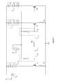
FIG. 1 is an example of light source circuitry in accordance with the present invention;
FIG. 2 is a graph illustrating the chromaticity of the light output by the circuitry of FIG. 1, when receiving various different control signals;
FIG. 3 is an alternative example of light source circuitry in accordance with the present invention;
FIG. 4 is a graph illustrating the chromaticity of the light output by the circuitry of FIG. 3 when receiving various different control signals; and
FIG. 5 is an alternative example of light source circuitry in accordance with the present invention.
DETAILED DESCRIPTION
In the following description, like reference numerals refer to like elements throughout.
FIG. 1 is an example of light source circuitry 1 in accordance with the present invention. The light source circuitry 1 comprises plural groups of LEDs 10, 12, 14. Specifically, the light source circuitry 1 of FIG. 1 comprises a first group of LEDs 10, a second group of LEDs 12 and a third group of LEDs 14. Each of the first, second and third groups of LEDs 10, 12, 14 comprises one or more LEDs e.g. 10A, 12A, 14A. Each of the groups of LEDs 10, 12, 14 is operable to emit light of a different color. In the example of FIG. 1, the first group of LEDs 10 consists of plural LEDs 10A, 10B, in this instance two, which are operable to emit lime-colored light (hereafter referred to as lime LEDs). The second group of LEDs 12 consists of plural LEDs 12A, 12 B 12C, in this example three, which are operable to emit red-colored light (hereafter referred to as red LEDs). The third group of LEDs 14 consists of plural LEDs 14A, 14B, 14C, in this instance three, which are operable to emit white-colored light (hereafter white LEDs). In this example, the LEDs within each of the first, second and third groups 10, 12, 14 are connected in series with one another.
The plural groups of LEDs 10, 12, 14 are connected in parallel with one another. As such, a fixed current arriving at the circuitry is shared among the plural groups of LEDs 10, 12, 14. The light source circuitry 1 also comprises a current source 70 which provides the fixed current. The light source circuitry 1 is configured such that a proportion of the fixed current that is provided to each of the first and second groups 10, 12 is controllable in dependence on a received control signal. The circuitry is also configured such that the remainder of the fixed current is provided to the third group 14.
In the specific example of FIG. 1, the light source circuitry 10 is configured such that when the control signal is at a first level, the majority of the fixed current flows through the white LEDs of the third group 14. As the control signal gradually moves towards a second level, the currents flowing through the lime and red LEDs of the first and second groups 10, 12 respectively both increase. Between the first and second levels, the current flowing through the lime LEDs 10A, 10B is larger than the current flowing through the red LEDs 12A, 12B, 12C. As the control signal gradually moves beyond the second level to a third level, the current in the lime LEDs 10A, 10B begins gradually to decrease, while the current in the red LEDs 12A, 12B, 12C continues to increase. The current flowing in the white LEDs 14A, 14B, 14C (i.e. the remainder of the current that is not flowing in the first and second groups 10, 12) gradually decreases as the control signal moves from the first to third levels. The current in the white LEDs 14A, 14B, 14C is nearly zero at the third level. At a point between the second and third levels, the current flowing in the second group 12 becomes larger than the current flowing in the first group 10. The light source circuitry 1 being configured in this way allows the chromaticity of the combined emissions of the first, second and third groups of LEDs 10, 12, 14 substantially to follow the Planckian locus (also known as the black body locus) as the control signal changes from the first to third levels.
The first group of LEDs 10 is connected in series with a first transistor 16. The second group of LEDs 12 is connected in series with a second transistor 18. In this example, the first and second transistors 16, 18 are n-channel bipolar junction transistors (BJTs). The base terminals of the first and second transistors 16, 18 are connected to one another via a first resistor 20. A first conductive path 19 connects the base terminal of the first transistor 16 and the first resistor 20. A second conductive path 21 connects the base terminal of the second transistor 16 and the first resistor 20. The presence of the first resistor 20 creates a dependency, so that the currents in the first and second groups of LEDs 10, 12 do not differ from one another by too much. This is achieved because the first resistor 20 limits the difference that can exist between the voltages at the base terminals of the first and second transistors 16, 18. However, in some alternative examples, the first resistor 20 may be omitted from the circuitry 1.
The light source circuitry 1 comprises a controllable voltage supply 22. This provides a voltage which acts as the control signal for varying the current that flows through the first and second groups of LEDs 10, 12. The controllable voltage supply 22 is connected to the base terminal of at least the second transistor 18 so as to vary the amount of current that flows through the second transistor 18, and thus also through the second group of LEDs 12. In this example, the controllable voltage supply is also connected to the base terminal of the first transistor 16 so as to vary the amount of current that flows through the first transistor 16, and thus also through the first group of LEDs 10.
The first group of LEDs 10 is connected to the collector terminal of the first transistor 16. The emitter terminal of the first transistor 16 is connected to ground, via a second resistor 64. The second group of LEDs 12 is connected to the collector terminal of the second transistor 18. The emitter terminal of the second transistor 18 is connected to ground, via a third resistor 68. The resistances of the second and third resistors 64, 68 are the same. The presence of the second and third resistors 64, 68 makes the circuit more stable over a range of different temperatures and between different instances of the light source circuitry 1. This is because their presence reduces the sensitivity to base-emitter voltage drift.
The third group of LEDs 14 is connected to ground. Whereas the current flowing through the first and second groups of LEDs 10, 12 is dependent on the control signal, the current through the third group of LEDs 14 is not directly controllable, but instead comprises the remainder of the first current that does not flow through the first and second groups 10, 12.
The controllable voltage supply 22 is connected to the base terminal of the second transistor 18 via first control circuitry 24A. The controllable voltage supply 22 is connected to the base terminal of the first transistor 16 via second control circuitry 24B. The first and second control circuitries 24A, 24B are configured so as to ensure that the combined light emissions of the first, second and third groups of LEDs 10, 12, 14 follows the Planckian locus as closely as possible for as long as possible. In the example of FIG. 1, this is achieved using analogue components, including diodes, resistors and transistors. However, it will be appreciated that it may instead be achieved using a micro-processor configured to receive a single voltage and to use this voltage to supply a suitable current to the base terminal of at least one of the first and second transistors 16, 18. Alternatively, this may be achieved using operational amplifiers.
In FIG. 1, the first control circuitry 24A comprises one or more, in this instance three, parallel circuit branches 26A, 26B, 26C connected between the controllable voltage supply 22 and the second conductive path 21. A first branch 26A comprises a fourth resistor 28. A second branch 26B comprises a fifth resistor 30 in series with a reverse-biased first Zener diode 32. A third branch 26C comprises a sixth resistor 34 in series with a reverse-biased second Zener diode 36. The presence of the first and second Zener diodes 32, 36 means that a significant current flows through the second and third branches 26B, 26C only when the potential difference between the controllable voltage supply 22 and the second conductive path 21 exceeds a predetermined value (i.e. the reverse voltage of the Zener diodes 32, 36). In contrast, current always flows through the first branch 26A as long as a potential difference exists. In this example, the first branch 26A is connected to the second conductive path 21 at a location nearest to the base terminal of the second transistor 18. The third branch 26C is connected to the second conductive path 21 at a location nearest to the first resistor 20. The second branch 26B is connected to the second conductive path 21 at a location between the locations at which the first and third branches 26A, 26C are connected to the second conductive path 21.
The second control circuitry 24B comprises one or more branches 38A, 38B, 38C, in this instance three, connected in parallel between the controllable voltage supply 22 and the first conductive path 19. A first branch 38A comprises a seventh resistor 40. A second branch 38B comprises a forward biased conventional diode 42 connected in series with an eighth resistor 44. A third branch 38C comprises a ninth resistor 46 in series with a third reverse-biased Zener diode 48. The presence of the first conventional diode in the second branch 38B means that a significant current will only flow in the second branch when the potential difference between the controllable voltage supply and the first conductive path 19 is above the forward voltage of the diode 42. The presence of the third Zener diode 48 means that a significant current will only flow in the third branch 38C when the potential difference is greater than the reverse voltage of the third Zener diode 48. A current will always flow in the first branch 38A as long as a potential difference exists. In this example, the second branch 38B is connected to the first conductive path 19 at a location nearest to the base terminal of the first transistor 16. The third branch 38C is connected to the first conductive path 19 at a location nearest to the first resistor 20. The first branch 38A is connected to the first conductive path 19 at a location between the locations at which the second and third branches 38B, 38C are connected to the first conductive path 19.
The second control circuitry 24B also comprises first and second control transistors 50, 52. In this example, the first and second control transistors 50, 52 comprise p-channel BJTs. The controllable voltage supply 22 is connected to the base terminal of the first control transistor 50 via a tenth resistor 54 connected in series with a fourth Zener diode 56. The controllable voltage supply 22 is connected to the base terminal of the second control transistor 52 via an eleventh resistor 58 connected in series with a fifth Zener diode 60. The collector of the first control transistor 50 is connected to the first conductive path 19, in this example at a location between the locations at which the first and third branches 38A, 38C of the second control circuitry 24B connect to the first conductive path 19. The emitter of the first control transistor 50 is connected to ground. The collector of the second control transistor 52 is connected to the base terminal of the first transistor 16, in this example at a location between the locations at which the first and second branches 38A, 38B of the second control circuitry 24B connect to the first conductive path 19. The emitter of the second control transistor 50 is connected to ground. The resistances of the tenth and eleventh resistors 45, 58 may be the same.
The presence of the first and second control transistors 50, 52 means that, when a potential difference between the base terminals of the first and second control transistors 50, 52 and the controllable voltage supply 22 is in excess of the reverse voltages of the fourth and fifth Zener diodes 56, 60, some current will flow through first and second control transistors from the first conductive path. As such, less current flows to the base terminal of the first transistor 16, and so less current flows through the collector-emitter junction of the first transistor 16 which means less current also flows through the first group of LEDs 10, thus reducing the intensity of the light emitted by the first group of LEDs 10.
Each of the first to fifth Zener diodes 32, 36, 48, 56, 60 may have a different reverse voltage. The reverse voltages of the Zener diodes 32, 36, 48, 56, 60 are selected based on the range of voltages of the control supply. Each of the Zener diodes is responsible for a change in the gradient of the chromaticity graph (see FIG. 2) of the light source circuitry 1. As such, the inclusion of the Zener diodes 32, 36, 48, 56, 60 allows the light source circuitry to track the Planckian Locus over a wider range of chromaticities. This will be apparent from a comparison of FIGS. 2 and 4.
Although not shown in the example of FIG. 1, the light source circuitry 1 may also comprise a current protection branch connected between the current source 70 and ground. Such a current protection branch may be connected in parallel with the first, second and third groups of LEDs 10, 12, 14. The current protection branch may comprise at least a resistor connected in series with a reverse-biased Zener diode. When, the potential difference between the current source 70 and ground exceeds the reverse voltage of the Zener diode, the current protection branch begins to conduct current. This reduces the amount of current that can flow through the first, second and third groups of LEDs 10, 12, 14 thereby protecting the LEDs against damage due to excessive currents.
In one example, the electrical components shown in FIG. 1 have the following electrical characteristics. It will be appreciated, however, that the below characteristics are examples only, and that components having different characteristics may instead be used:
  • resistance of the first resistor 20=15,000 Ohms (Ω);
  • resistance of the second resistor 64=0.68Ω;
  • resistance of the third resistor 68=0.68Ω;
  • resistance of the fourth resistor 28=2,400Ω;
  • resistance of the fifth resistor 30=1,800Ω;
  • resistance of the sixth resistor 32=220,000Ω;
  • resistance of the seventh resistor 40=4,200Ω;
  • resistance of the eighth resistor 44=1100Ω;
  • resistance of the ninth resistor 46=220,000Ω;
  • resistance of the tenth resistor 54=82,000Ω;
  • resistance of the eleventh resistor 58=82,000Ω;
  • forward voltages of the lime LEDs 10A, 10B=3 Volts (V) each;
  • forward voltages of the red LEDs 12A, 12B, 12C=2.4V each;
  • forward voltages of the white LEDs 14A, 14B, 14C=3V each;
  • forward voltage of the diode 42=0.6V;
  • reverse voltage of the first Zener diode 32=3.3V
  • reverse voltage of the second Zener diode 36=4.7V
  • reverse voltage of the third Zener diode 48=5.1V
  • reverse voltage of the fourth Zener diode 56=9.1V
  • reverse voltage of the fifth Zener diode 60=15V; and
  • current provided by current source 70=700 mA.
Table 1, below, shows the currents flowing through the lime, red and white LEDs in light source circuitry 1 having the above characteristics for a varying control signal:
TABLE 1
Control Signal (V) ILIME (A) IRED (A) IWHITE (A)
1.0 0.012 0.015 0.673
1.5 0.036 0.03 0.634
2.0 0.056 0.04 0.604
2.5 0.086 0.055 0.559
3.0 0.125 0.075 0.5
3.5 0.173 0.1 0.427
4.0 0.221 0.13 0.349
4.5 0.252 0.165 0.283
5.0 0.293 0.21 0.197
5.5 0.318 0.255 0.127
6.0 0.323 0.305 0.072
6.5 0.326 0.35 0.024
7.0 0.298 0.38 0.022
7.5 0.28 0.41 0.01
8.0 0.25 0.44 0.01
From Table 1 it can be seen that, in this example, the first control signal level is between 1.0 and 1.5V. The second control signal level, at which the current flowing through the lime LEDs 10A, 10B, 10C, begins to drop is located between 6.5V and 7.0V.
Table 2, below, shows the chromaticity and the flux levels of the combined emissions of the first, second and third groups of LEDs 10, 12, 14 as the control signal changes gradually from a first level to the third level.
TABLE 2
Control Signal (V) Cx Cy Flux (Lumen)
1.0 0.333774 0.343104 450.8929274
1.5 0.341650 0.349198 465.1289412
2.0 0.346767 0.353348 472.9506647
2.5 0.353973 0.358896 481.0644331
3.0 0.363155 0.365567 487.3098279
3.5 0.374633 0.373591 490.2112517
4.0 0.388160 0.381987 487.529364
4.5 0.402408 0.388265 478.5973982
5.0 0.423588 0.398195 462.2534738
5.5 0.446396 0.407129 440.775934
6.0 0.472420 0.413898 413.0114279
6.5 0.503973 0.422884 379.8113722
7.0 0.513653 0.417157 364.758582
7.5 0.531780 0.415718 342.1999935
From Table 2, it can be seen that the flux levels produced by the light source circuitry of FIG. 1 is reasonably constant. The variation in the flux levels at different control signals is caused by the differences in efficiency between the LEDs of different colors.
The chromaticities of Table 2 can be seen in graphical form in FIG. 2 and are shown by the squares connected by the line marked G1. FIG. 2 also shows, by way of comparison, the Planckian locus, which is denoted by the line marked PL. It can, thus, be seen, that the chromaticity of the light source system substantially follows the Planckian locus.
As will be understood from the above description, light source circuitry in accordance with the present invention allows the tint or color of light produced by the light source circuitry to be varied without the need to use PWM. In addition, it requires only a variation in a single control signal to obtain a wide range of different tints or colors, which in some embodiments follow closely the Planckian locus. The structural simplicity of the light source circuitry, and the fact that it needs only a single control signal to vary the tint across a wide range of chromaticities, means that the cost of manufacture of the light source circuitry and any appliance, such as a bulb, which includes the light source circuitry can remain relatively low.
FIG. 3 shows an uncompensated version 3 of the light source circuitry of FIG. 1. The uncompensated light source circuitry 3 is substantially the same as the circuitry 1 of FIG. 1 except that it includes much simplified control circuitries 24A, 24B. Specifically, the first control circuitry 24A is constituted by a resistor 27 connected between the controllable voltage supply 22 and the second conductive path 21. The second control circuitry 24B is constituted by a resistor 39 connected between the controllable voltage supply 22 and the first conductive path 21.
FIG. 4 shows a graph of the chromaticity of the combined emissions of light source circuitry 3 of FIG. 3 (denoted G2) relative to the Planckian Locus (denoted PL). As can be seen, the combined emissions still track the Planckian Locus, but over a shorter range of chromaticities. For the generation of the chromaticities shown in FIG. 4, the electrical characteristics of the components of the light source circuitry 3 were the same as the characteristics of the corresponding components listed above with reference to FIG. 1 (i.e. the resistances of the resistors 20, 64 and 68 were the same, as well as the forward voltages of the LEDs 10, 12, 14, and the voltage and current of the controllable voltage and current sources 22, 70 respectively). The resistance of the resistor 27 of the first control circuitry 24A was 4,200Ω. The resistance of the resistor 39 of the second control circuitry 24B was 2,400Ω.
FIG. 5 is an example of another alternative arrangement of light source circuitry 150 in accordance with the invention.
The light source circuitry 5 of FIG. 5 is substantially the same as the uncompensated light source circuitry of FIG. 3. However, the light source circuitry 5 of FIG. 5 also comprises a third transistor 500 connected in series with the third group of LEDs 14. In the example of FIG. 5, the third group of LEDs are connected to the collector terminal of the third transistor 500. The emitter terminal of the third transistor 500 is connected to ground. The controllable voltage supply 22 is connected to the base terminal of the third transistor 500. The connection between the controllable voltage supply 22 and the base terminal of the third transistor 500 may include no resistor, or may include a resistor that is of significantly lower resistance than the resistors 27, 39 of the first and second control circuitries 24A, 24B. This means that a higher current flows through the base-emitter junction of the third transistor than through the base-emitter junctions of the first and second transistors 16, 18. As such, the current flow through the collector-emitter junction of the third transistor 500 is less restricted than are the current flows through the collector-emitter junctions of the first and second transistors 16, 18. At low control signals, the current flows through the base-emitter junctions of the first to third transistors 16, 18, 500 are such that most of the current supplied to the circuitry 5 flows through the third transistor 500, and so also through the third group of LEDs 14.
Similarly to the examples of FIGS. 1 and 3, the light source circuitry 5 of FIG. 5 is configured such that when the control signal is at a first level, the majority of the current flows through the white LEDs of the third group 14. As the control signal gradually moves towards a second level, the currents flowing through the lime and red LEDs of the first second groups 10, 12 respectively both increase. The current flowing through the LEDs in the first group 10 is larger than the current flowing through the LEDs of the second group 12. In this example, the current flowing through the second group of LEDs 12 never becomes larger than the current flowing through first group of LEDs 10. As such, the combined emission of the light source circuitry 5 follows the Planckian locus over a shorter range of chromaticities than does the example of FIG. 1. The current flowing in the third group 14 (i.e. the remainder of the current that is not flowing in the first and second groups 10, 12) gradually decreases as the control signal moves from the first to third levels. The light source circuitry 5 of FIG. 5 operates in this way at least in part because the combined forward voltage of the third group of LEDs 14 is greater than the forward voltages of the first and second groups of LEDs 10, 12. The forward voltage of the second group of LEDs 12 is preferably similar to the forward voltage of the first group of LEDs 10.
In one example, the characteristics of the components of the circuitry 5 of FIG. 5 are substantially the same as those in FIG. 3, except that the resistance of the resistor 27 of the first control circuitry 24A is 2,400Ω and the resistance of the resistor 39 of the second control circuitry 24B is 3000Ω
Although the specific examples of FIGS. 1, 3 and 5 show the fixed current source 70 as part of the light source circuitry 1, 3, 5, it will be appreciated that this may be separable. As such, the circuitry 1, 3, 5 may instead be configured to be connectable to (and so not actually including) the fixed current source 70. The fixed current source 70 may comprise, for example, a mains-power flyback converter. Alternatively, the fixed current source 70 may comprise any other means for providing a fixed current to the light source circuitry 1, 3, 5.
Similarly, the controllable voltage source 22 for providing the control signal may be separate or separable from the light source circuitry 1, 3, 5. The controllable voltage source 22 may comprise, for example, a rectified mains signal with, for example, an output voltage between 1V and 10V.
Although the examples of FIGS. 1, 3 and 5 show the groups of LEDs 10, 12, 14 connected to the collector terminals of the various transistors 16, 18, 500, it will be understood that the groups of LEDs may instead be connected to the emitter terminals. Also, although the specific examples include n-channel BJTs, in some examples p-channel BJTs may be used. Alternatively, field effect transistors may be used. In examples which include field-effect transistors, where a connection is described above as being to the base terminal, the connection is instead to the gate terminal. Similarly, where a connection is described as being with the emitter terminal or collector terminal, in examples including field-effect transistors the connection is instead to the drain or source terminals respectively. The gate terminal and the base terminal of field-effect transistors and BJTs respectively may be collectively referred to herein as control terminals. This is because a signal provided to those terminals controls the current that flows through the transistor.
It will be appreciated, that each of the groups of LEDs 10, 12, 14 may include LEDs of different colors, the combined emissions of which result in light of a desired color. For example, the first group of LEDs 14, instead of all being Lime LEDs, may be comprised of a mixture of green LEDs and amber LEDs to produce a lime-colored combined emission.
In the examples above, the colors and quantities of LEDs are selected so as to be able to produce a combined emission that closely follows the Planckian locus. However, in other examples, different colored LEDs to those described above may used. Similarly, different numbers of LEDs to those described above may be used. Also, although the Figures show the LEDs of each group connected in series, in some alternatives the LEDs of each group may be connected in parallel, or in a combination of in series an in parallel. It will be obvious to the skilled person that the light source circuitry according to the present invention, may be used to create LED light sources such as retrofit lamps, LED luminaires, or lamp for professional applications such as lamps used in theaters or lamps for illuminating steps.
It will be appreciated that the term “comprising” does not exclude other elements or steps and that the indefinite article “a” or “an” does not exclude a plurality. A single processor may fulfill the functions of several items recited in the claims. The mere fact that certain measures are recited in mutually different dependent claims does not indicate that a combination of these measures cannot be used to an advantage. Any reference signs in the claims should not be construed as limiting the scope of the claims.
Although claims have been formulated in this application to particular combinations of features, it should be understood that the scope of the disclosure of the present invention also includes any novel features or any novel combinations of features disclosed herein either explicitly or implicitly or any generalization thereof, whether or not it relates to the same invention as presently claimed in any claim and whether or not it mitigates any or all of the same technical problems as does the parent invention. The applicants hereby give notice that new claims may be formulated to such features and/or combinations of features during the prosecution of the present application or of any further application derived there from.
Other modifications and variations falling within the scope of the claims hereinafter will be evident to those skilled in the art.

Claims (14)

The invention claimed is:
1. Light source circuitry comprising:
a first group of one or more light emitting diodes configured to emit light of a first color;
a second group of one or more light emitting diodes configured to emit light of a second color;
a third group of one or more light emitting diodes configured to emit light of a third color, wherein the first, second and third groups of light emitting diodes are configured such that, when a fixed current arrives at the light source circuitry, the fixed current is shared between the first, second and third groups;
a first transistor connected in series with the first group of light emitting diodes; and
a second transistor connected in series with the second group of light emitting diodes, wherein the first transistor and second transistor are configured such that a variation in a single received control signal causes a variation in a first proportion of the fixed current that flows through the first transistor and causes a variation in a second proportion of the fixed current that flows through the second transistor, such that the proportions of the fixed current that flow through each of the first and second groups is controllable in dependence on the single received control signal and such that the remainder of the fixed current flows through the third group;
wherein the light source circuitry is configured such that a first signal based on the control signal is provided to the control terminal of the first transistor and such that a second signal based on the control signal is provided to the control terminal of the second transistor;
wherein the light source circuitry is further configured such that, when the control signal is at a first level, the largest proportion of the fixed current flows through the third group of light emitting diodes and such that, as the control signal changes to a second level, the proportions of the fixed current that flow through the first and second groups of light emitting diodes increase.
2. The light source circuitry of claim 1, wherein the light source circuitry is configured such that the first and second signals based on the control signal vary relative to one another in dependence on the control signal.
3. The light source circuitry of claim 1, further comprising a third transistor connected in series with the third group of light emitting diodes.
4. The light source circuitry of claim 3, wherein a third signal based on the control signal is received at the control terminal of the third transistor, wherein the third signal is always larger than the first and second signals.
5. The light source circuitry of claim 1, wherein the combined forward voltage of the third group of light emitting diodes is larger than the combined forward voltage of the first group of light emitting diodes and the combined forward voltage of the second group of light emitting diodes.
6. The light source circuitry of claim 1, wherein the light source circuitry is configured such that, as the control signal changes from the second level to a third level, the proportion of the fixed current that flows in the first group of light emitting diodes decreases, and the proportion of the fixed current that flows in the second group of light emitting diodes continues to increase.
7. The light source circuitry of claim 1, wherein:
the second group is constituted by one or more light emitting diodes operable to emit red-colored light;
the third group is constituted by one or more light emitting diodes operable to emit white-colored light; and
the first group of light emitting diodes is constituted by one or more light emitting diodes the combined emission of which is lime-colored.
8. The light source circuitry of claim 1, wherein the light source circuitry is configured such that, as the control signal gradually changes from a first level to a different level, the color of the combined emissions of the first, second and third groups of light emitting diodes changes generally in accordance with the Planckian locus.
9. A LED light source comprising light source circuitry according to claim 1.
10. A method of manufacturing light source circuitry comprising:
providing a first group of one or more light emitting diodes configured to emit light of a first color;
providing a second group of one or more light emitting diodes configured to emit light of a second color;
providing a third group of one or more light emitting diodes configured to emit light of third color,
configuring the first, second and third groups of light emitting diodes such that, when a fixed current arrives at the light source circuitry, the fixed current is shared between the first, second and third groups;
providing a first transistor connected in series with the first group of light emitting diodes;
providing a second transistor connected in series with the second group of light emitting diodes; and
configuring the first transistor and the second transistor such that a variation in a single received control signal causes a variation in a first proportion of the fixed current that flows through the first transistor and causes a variation in a second proportion of the fixed current that flows through the second transistor, such that the proportions of the fixed current that flow through each of the first and second groups is controllable in dependence on the single received control signal and such that the remainder of the fixed current flows through the third group;
configuring the light source circuitry such that, when the control signal is at a first level, the largest proportion of the fixed current flows through the third group of light emitting diodes and such that, as the control signal changes to a second level, the proportions of the fixed current that flow through the first and second groups of light emitting diodes increase; and
providing a first signal based on the control signal to a control terminal of the first transistor and providing a second signal based on the control signal to a control terminal of the second transistor.
11. Light control circuitry comprising:
a controllable voltage supply configured to provide a single control signal;
a first transistor connected in series with a first group of light emitting diodes configured to emit light of a first color; and
a first control circuitry comprising at least one parallel circuit branch connected to the controllable voltage supply and the first transistor;
a second transistor connected in series with a second group of light emitting diodes configured to emit light of a second color, and in parallel with a third group of light emitting diodes configured to emit light of a third color;
a second control circuitry comprising at least one parallel circuit branch connected to the controllable voltage supply and to the second transistor;
wherein a fixed current is shared between the first, second and third groups, and
wherein the first and second control circuitry is configured such that a variation in the single control signal causes a variation in a first proportion of the fixed current that flows through the first transistor and causes a variation in a second proportion of the fixed current that flows through the second transistor,
wherein the first and second control circuitry is configured such that a first signal based on the control signal is provided to the control terminal of the first transistor and such that a second signal based on the control signal is provided to the control terminal of the second transistor.
12. The light control circuitry of claim 11, wherein the first and second control circuitry is configured such that, when the control signal is at a first level, the largest proportion of the fixed current flows through the third group of light emitting diodes and such that, as the control signal changes to second level, the proportions of the fixed current that flow through the first and second groups of light emitting diodes increase.
13. The light control circuitry of claim 11, wherein the controllable voltage supply is connected to the second transistor via the first control circuitry and the controllable voltage supply is connected to the first transistor via the second control circuitry.
14. The light control circuitry of claim 11, wherein the first and second control circuitry is configured such that, as the control signal gradually changes from a first level to a different level, the color of the combined emissions of the first, second and third groups of light emitting diodes changes generally in accordance with the Planckian locus.
US14/400,088 2012-05-15 2013-05-06 Light source circuitry for controlling the color of emitted light Active US9504115B2 (en)

Priority Applications (1)

Application Number Priority Date Filing Date Title
US14/400,088 US9504115B2 (en) 2012-05-15 2013-05-06 Light source circuitry for controlling the color of emitted light

Applications Claiming Priority (3)

Application Number Priority Date Filing Date Title
US201261646934P 2012-05-15 2012-05-15
PCT/IB2013/053619 WO2013171622A1 (en) 2012-05-15 2013-05-06 Light source circuitry
US14/400,088 US9504115B2 (en) 2012-05-15 2013-05-06 Light source circuitry for controlling the color of emitted light

Publications (2)

Publication Number Publication Date
US20150108919A1 US20150108919A1 (en) 2015-04-23
US9504115B2 true US9504115B2 (en) 2016-11-22

Family

ID=48628757

Family Applications (1)

Application Number Title Priority Date Filing Date
US14/400,088 Active US9504115B2 (en) 2012-05-15 2013-05-06 Light source circuitry for controlling the color of emitted light

Country Status (6)

Country Link
US (1) US9504115B2 (en)
EP (1) EP2850917B1 (en)
JP (1) JP6389457B2 (en)
CN (1) CN104303597B (en)
PL (1) PL2850917T3 (en)
WO (1) WO2013171622A1 (en)

Cited By (1)

* Cited by examiner, † Cited by third party
Publication number Priority date Publication date Assignee Title
US11917737B2 (en) 2021-08-02 2024-02-27 Bio-Rad Laboratories, Inc. Circuit for sharing current between parallel LEDs or parallel strings of LEDs

Families Citing this family (3)

* Cited by examiner, † Cited by third party
Publication number Priority date Publication date Assignee Title
EP3314982B1 (en) * 2015-06-25 2018-12-05 Philips Lighting Holding B.V. Led lighting arrangement
DE102016125457A1 (en) 2015-12-25 2017-06-29 Panasonic Intellectual Property Management Co., Ltd. Illumination light communication device and communication module
US10104730B2 (en) * 2017-03-07 2018-10-16 B/E Aerospace, Inc. LED bulb and method for operating same

Citations (20)

* Cited by examiner, † Cited by third party
Publication number Priority date Publication date Assignee Title
US6305818B1 (en) 1998-03-19 2001-10-23 Ppt Vision, Inc. Method and apparatus for L.E.D. illumination
US20030025120A1 (en) * 2001-08-03 2003-02-06 Koninklijke Philips Electronics N.V. Integrated LED driving device with current sharing for multiple LED strings
US6538394B2 (en) * 2001-03-30 2003-03-25 Maxim Integrated Products, Inc. Current source methods and apparatus for light emitting diodes
US6864641B2 (en) * 2003-02-20 2005-03-08 Visteon Global Technologies, Inc. Method and apparatus for controlling light emitting diodes
US20060049782A1 (en) 2004-09-08 2006-03-09 Vornsand Steven J Lighting apparatus having a plurality of independently controlled sources of different colors of light
US7122971B2 (en) * 2003-11-05 2006-10-17 Richtek Technology Corp. Driver circuit for driving a plurality of DC lamp strings
US20070080911A1 (en) 2005-10-11 2007-04-12 Da Liu Controller circuitry for light emitting diodes
US20070152909A1 (en) 2006-01-05 2007-07-05 Sanyo Electric Co., Ltd. Led device
US20070205968A1 (en) 2006-03-03 2007-09-06 Pei-Ming Chen Organic light-emitting diode display, organic light-emitting diode panel and driving device thereof
US20080116817A1 (en) * 2006-11-16 2008-05-22 Han-Yu Chao Controlling apparatus for controlling a plurality of led strings and related light modules
JP2009152518A (en) * 2007-11-30 2009-07-09 Omron Corp Light emitting diode driving device
US20090322234A1 (en) * 2008-06-30 2009-12-31 Iwatt Inc. Led driver with multiple feedback loops
US20100164403A1 (en) * 2008-12-31 2010-07-01 O2Micro, Inc. Circuits and methods for controlling LCD backlights
WO2010122463A1 (en) 2009-04-23 2010-10-28 Koninklijke Philips Electronics N.V. Driver for an led lamp
US20110080115A1 (en) * 2009-10-01 2011-04-07 Liangan Ge Constant current control circuit with multiple outputs for led driver
US20110199019A1 (en) 2010-02-16 2011-08-18 Mcclear Mark Color control of light emitting devices and applications thereof
US20120223657A1 (en) * 2011-03-03 2012-09-06 Cree, Inc. Semiconductor Light Emitting Devices Having Selectable And/or Adjustable Color Points and Related Methods
US20130154484A1 (en) * 2011-12-19 2013-06-20 Peng Xu LED Driving System for Driving Multi-String LEDS and the Method Thereof
US20130278151A1 (en) * 2012-04-20 2013-10-24 Trilumina Corporation Addressable illuminator with eye-safety circuitry
US9018845B2 (en) * 2011-04-02 2015-04-28 Inventronics (Hangzhou), Inc. Circuit for adjusting LED current

Family Cites Families (3)

* Cited by examiner, † Cited by third party
Publication number Priority date Publication date Assignee Title
JPH11298044A (en) * 1998-04-16 1999-10-29 Sony Corp Light source drive circuit
JP2007059260A (en) * 2005-08-25 2007-03-08 Toshiba Lighting & Technology Corp Illumination device and illumination fixture
JP5462535B2 (en) * 2009-06-25 2014-04-02 パナソニック株式会社 Lighting device

Patent Citations (21)

* Cited by examiner, † Cited by third party
Publication number Priority date Publication date Assignee Title
US6305818B1 (en) 1998-03-19 2001-10-23 Ppt Vision, Inc. Method and apparatus for L.E.D. illumination
US6538394B2 (en) * 2001-03-30 2003-03-25 Maxim Integrated Products, Inc. Current source methods and apparatus for light emitting diodes
US20030025120A1 (en) * 2001-08-03 2003-02-06 Koninklijke Philips Electronics N.V. Integrated LED driving device with current sharing for multiple LED strings
US6621235B2 (en) * 2001-08-03 2003-09-16 Koninklijke Philips Electronics N.V. Integrated LED driving device with current sharing for multiple LED strings
US6864641B2 (en) * 2003-02-20 2005-03-08 Visteon Global Technologies, Inc. Method and apparatus for controlling light emitting diodes
US7122971B2 (en) * 2003-11-05 2006-10-17 Richtek Technology Corp. Driver circuit for driving a plurality of DC lamp strings
US20060049782A1 (en) 2004-09-08 2006-03-09 Vornsand Steven J Lighting apparatus having a plurality of independently controlled sources of different colors of light
US20070080911A1 (en) 2005-10-11 2007-04-12 Da Liu Controller circuitry for light emitting diodes
US20070152909A1 (en) 2006-01-05 2007-07-05 Sanyo Electric Co., Ltd. Led device
US20070205968A1 (en) 2006-03-03 2007-09-06 Pei-Ming Chen Organic light-emitting diode display, organic light-emitting diode panel and driving device thereof
US20080116817A1 (en) * 2006-11-16 2008-05-22 Han-Yu Chao Controlling apparatus for controlling a plurality of led strings and related light modules
JP2009152518A (en) * 2007-11-30 2009-07-09 Omron Corp Light emitting diode driving device
US20090322234A1 (en) * 2008-06-30 2009-12-31 Iwatt Inc. Led driver with multiple feedback loops
US20100164403A1 (en) * 2008-12-31 2010-07-01 O2Micro, Inc. Circuits and methods for controlling LCD backlights
WO2010122463A1 (en) 2009-04-23 2010-10-28 Koninklijke Philips Electronics N.V. Driver for an led lamp
US20110080115A1 (en) * 2009-10-01 2011-04-07 Liangan Ge Constant current control circuit with multiple outputs for led driver
US20110199019A1 (en) 2010-02-16 2011-08-18 Mcclear Mark Color control of light emitting devices and applications thereof
US20120223657A1 (en) * 2011-03-03 2012-09-06 Cree, Inc. Semiconductor Light Emitting Devices Having Selectable And/or Adjustable Color Points and Related Methods
US9018845B2 (en) * 2011-04-02 2015-04-28 Inventronics (Hangzhou), Inc. Circuit for adjusting LED current
US20130154484A1 (en) * 2011-12-19 2013-06-20 Peng Xu LED Driving System for Driving Multi-String LEDS and the Method Thereof
US20130278151A1 (en) * 2012-04-20 2013-10-24 Trilumina Corporation Addressable illuminator with eye-safety circuitry

Non-Patent Citations (1)

* Cited by examiner, † Cited by third party
Title
Ivan Moreno; "Color Tunable Hybrid Lamp: LED-Incandescent and LED-Fluorescent", Sixth Symposium Optics Industry, Proc. of SPIE, vol. 6422, No. 1, 2007, pp. 1-7.

Cited By (1)

* Cited by examiner, † Cited by third party
Publication number Priority date Publication date Assignee Title
US11917737B2 (en) 2021-08-02 2024-02-27 Bio-Rad Laboratories, Inc. Circuit for sharing current between parallel LEDs or parallel strings of LEDs

Also Published As

Publication number Publication date
US20150108919A1 (en) 2015-04-23
WO2013171622A1 (en) 2013-11-21
PL2850917T3 (en) 2017-08-31
CN104303597B (en) 2017-12-15
JP6389457B2 (en) 2018-09-12
EP2850917A1 (en) 2015-03-25
CN104303597A (en) 2015-01-21
JP2015522903A (en) 2015-08-06
EP2850917B1 (en) 2017-02-22

Similar Documents

Publication Publication Date Title
US9730291B1 (en) Color temperature adjustment based on dim level
US9320097B2 (en) Multi-string dimmable LED driver
US8004211B2 (en) LED lighting device
US8277078B2 (en) Light emitting device
US10182486B2 (en) LED drive circuit
US20140217907A1 (en) Solid state lighting apparatus including separately driven led strings and methods of operating the same
US20130147359A1 (en) Lighting Devices Including Current Shunting Responsive To LED Nodes And Related Methods
US11812525B2 (en) Methods and apparatus for controlling the current supplied to light emitting diodes
US20140210361A1 (en) Linear bypass electrical circuit for driving led strings
WO2013118208A1 (en) Light-emitting circuit, light-emitting module, and illumination device
US9504115B2 (en) Light source circuitry for controlling the color of emitted light
US10750592B1 (en) Systems and methods for controlling color temperature and brightness of LED lighting using two wires
CN110958731A (en) Light emitting diode parallel circuit
JP5454189B2 (en) Power supply circuit and lighting device
US20090108772A1 (en) Color-temperature adjustable light-emitting device and control circuitry thereof
JP6411261B2 (en) LED drive circuit
JP2012169195A (en) Led lighting control turn-on device
US7352137B2 (en) Controlling color temperature of lighting fixture
US20220386431A1 (en) A light emitting diode, led, based lighting device arranged for emitting a particular emitted light following a planckian locus in a color space
CN211297029U (en) Control circuit of one-way double-color temperature
CN110636670B (en) Light source device
CN210928058U (en) LED lamp color temperature and brightness linear control circuit
JP2015008275A (en) Led module device and led lighting device
JP2020030905A (en) Led light-emitting device
CN110856303A (en) LED lamp color temperature and brightness linear control circuit

Legal Events

Date Code Title Description
AS Assignment

Owner name: KONINKLIJKE PHILIPS ELECTRONICS N.V., NETHERLANDS

Free format text: ASSIGNMENT OF ASSIGNORS INTEREST;ASSIGNOR:VAN ERP, JOSEPHUS ADRIANUS MARIA;REEL/FRAME:034135/0823

Effective date: 20131030

AS Assignment

Owner name: PHILIPS LIGHTING HOLDING B.V., NETHERLANDS

Free format text: ASSIGNMENT OF ASSIGNORS INTEREST;ASSIGNOR:KONINKLIJKE PHILIPS N.V.;REEL/FRAME:040060/0009

Effective date: 20160607

STCF Information on status: patent grant

Free format text: PATENTED CASE

AS Assignment

Owner name: SIGNIFY HOLDING B.V., NETHERLANDS

Free format text: CHANGE OF NAME;ASSIGNOR:PHILIPS LIGHTING HOLDING B.V.;REEL/FRAME:050837/0576

Effective date: 20190201

MAFP Maintenance fee payment

Free format text: PAYMENT OF MAINTENANCE FEE, 4TH YEAR, LARGE ENTITY (ORIGINAL EVENT CODE: M1551); ENTITY STATUS OF PATENT OWNER: LARGE ENTITY

Year of fee payment: 4