US9511449B2 - Laser processing method and device - Google Patents
Laser processing method and device Download PDFInfo
- Publication number
- US9511449B2 US9511449B2 US14/099,236 US201314099236A US9511449B2 US 9511449 B2 US9511449 B2 US 9511449B2 US 201314099236 A US201314099236 A US 201314099236A US 9511449 B2 US9511449 B2 US 9511449B2
- Authority
- US
- United States
- Prior art keywords
- lens
- laser beam
- processing
- laser
- main surface
- Prior art date
- Legal status (The legal status is an assumption and is not a legal conclusion. Google has not performed a legal analysis and makes no representation as to the accuracy of the status listed.)
- Active
Links
Images


Classifications
-
- B—PERFORMING OPERATIONS; TRANSPORTING
- B23—MACHINE TOOLS; METAL-WORKING NOT OTHERWISE PROVIDED FOR
- B23K—SOLDERING OR UNSOLDERING; WELDING; CLADDING OR PLATING BY SOLDERING OR WELDING; CUTTING BY APPLYING HEAT LOCALLY, e.g. FLAME CUTTING; WORKING BY LASER BEAM
- B23K26/00—Working by laser beam, e.g. welding, cutting or boring
- B23K26/02—Positioning or observing the workpiece, e.g. with respect to the point of impact; Aligning, aiming or focusing the laser beam
- B23K26/04—Automatically aligning, aiming or focusing the laser beam, e.g. using the back-scattered light
- B23K26/046—Automatically focusing the laser beam
- B23K26/048—Automatically focusing the laser beam by controlling the distance between laser head and workpiece
-
- B23K26/0057—
-
- B—PERFORMING OPERATIONS; TRANSPORTING
- B23—MACHINE TOOLS; METAL-WORKING NOT OTHERWISE PROVIDED FOR
- B23K—SOLDERING OR UNSOLDERING; WELDING; CLADDING OR PLATING BY SOLDERING OR WELDING; CUTTING BY APPLYING HEAT LOCALLY, e.g. FLAME CUTTING; WORKING BY LASER BEAM
- B23K26/00—Working by laser beam, e.g. welding, cutting or boring
- B23K26/02—Positioning or observing the workpiece, e.g. with respect to the point of impact; Aligning, aiming or focusing the laser beam
- B23K26/04—Automatically aligning, aiming or focusing the laser beam, e.g. using the back-scattered light
- B23K26/046—Automatically focusing the laser beam
-
- B—PERFORMING OPERATIONS; TRANSPORTING
- B23—MACHINE TOOLS; METAL-WORKING NOT OTHERWISE PROVIDED FOR
- B23K—SOLDERING OR UNSOLDERING; WELDING; CLADDING OR PLATING BY SOLDERING OR WELDING; CUTTING BY APPLYING HEAT LOCALLY, e.g. FLAME CUTTING; WORKING BY LASER BEAM
- B23K26/00—Working by laser beam, e.g. welding, cutting or boring
- B23K26/02—Positioning or observing the workpiece, e.g. with respect to the point of impact; Aligning, aiming or focusing the laser beam
- B23K26/06—Shaping the laser beam, e.g. by masks or multi-focusing
- B23K26/064—Shaping the laser beam, e.g. by masks or multi-focusing by means of optical elements, e.g. lenses, mirrors or prisms
- B23K26/0643—Shaping the laser beam, e.g. by masks or multi-focusing by means of optical elements, e.g. lenses, mirrors or prisms comprising mirrors
-
- B—PERFORMING OPERATIONS; TRANSPORTING
- B23—MACHINE TOOLS; METAL-WORKING NOT OTHERWISE PROVIDED FOR
- B23K—SOLDERING OR UNSOLDERING; WELDING; CLADDING OR PLATING BY SOLDERING OR WELDING; CUTTING BY APPLYING HEAT LOCALLY, e.g. FLAME CUTTING; WORKING BY LASER BEAM
- B23K26/00—Working by laser beam, e.g. welding, cutting or boring
- B23K26/02—Positioning or observing the workpiece, e.g. with respect to the point of impact; Aligning, aiming or focusing the laser beam
- B23K26/06—Shaping the laser beam, e.g. by masks or multi-focusing
- B23K26/064—Shaping the laser beam, e.g. by masks or multi-focusing by means of optical elements, e.g. lenses, mirrors or prisms
- B23K26/0648—Shaping the laser beam, e.g. by masks or multi-focusing by means of optical elements, e.g. lenses, mirrors or prisms comprising lenses
-
- B—PERFORMING OPERATIONS; TRANSPORTING
- B23—MACHINE TOOLS; METAL-WORKING NOT OTHERWISE PROVIDED FOR
- B23K—SOLDERING OR UNSOLDERING; WELDING; CLADDING OR PLATING BY SOLDERING OR WELDING; CUTTING BY APPLYING HEAT LOCALLY, e.g. FLAME CUTTING; WORKING BY LASER BEAM
- B23K26/00—Working by laser beam, e.g. welding, cutting or boring
- B23K26/08—Devices involving relative movement between laser beam and workpiece
- B23K26/083—Devices involving movement of the workpiece in at least one axial direction
-
- B—PERFORMING OPERATIONS; TRANSPORTING
- B23—MACHINE TOOLS; METAL-WORKING NOT OTHERWISE PROVIDED FOR
- B23K—SOLDERING OR UNSOLDERING; WELDING; CLADDING OR PLATING BY SOLDERING OR WELDING; CUTTING BY APPLYING HEAT LOCALLY, e.g. FLAME CUTTING; WORKING BY LASER BEAM
- B23K26/00—Working by laser beam, e.g. welding, cutting or boring
- B23K26/36—Removing material
- B23K26/38—Removing material by boring or cutting
-
- B—PERFORMING OPERATIONS; TRANSPORTING
- B23—MACHINE TOOLS; METAL-WORKING NOT OTHERWISE PROVIDED FOR
- B23K—SOLDERING OR UNSOLDERING; WELDING; CLADDING OR PLATING BY SOLDERING OR WELDING; CUTTING BY APPLYING HEAT LOCALLY, e.g. FLAME CUTTING; WORKING BY LASER BEAM
- B23K26/00—Working by laser beam, e.g. welding, cutting or boring
- B23K26/36—Removing material
- B23K26/40—Removing material taking account of the properties of the material involved
-
- B—PERFORMING OPERATIONS; TRANSPORTING
- B23—MACHINE TOOLS; METAL-WORKING NOT OTHERWISE PROVIDED FOR
- B23K—SOLDERING OR UNSOLDERING; WELDING; CLADDING OR PLATING BY SOLDERING OR WELDING; CUTTING BY APPLYING HEAT LOCALLY, e.g. FLAME CUTTING; WORKING BY LASER BEAM
- B23K26/00—Working by laser beam, e.g. welding, cutting or boring
- B23K26/50—Working by transmitting the laser beam through or within the workpiece
- B23K26/53—Working by transmitting the laser beam through or within the workpiece for modifying or reforming the material inside the workpiece, e.g. for producing break initiation cracks
-
- B—PERFORMING OPERATIONS; TRANSPORTING
- B28—WORKING CEMENT, CLAY, OR STONE
- B28D—WORKING STONE OR STONE-LIKE MATERIALS
- B28D5/00—Fine working of gems, jewels, crystals, e.g. of semiconductor material; apparatus or devices therefor
- B28D5/0005—Fine working of gems, jewels, crystals, e.g. of semiconductor material; apparatus or devices therefor by breaking, e.g. dicing
- B28D5/0011—Fine working of gems, jewels, crystals, e.g. of semiconductor material; apparatus or devices therefor by breaking, e.g. dicing with preliminary treatment, e.g. weakening by scoring
-
- H—ELECTRICITY
- H01—ELECTRIC ELEMENTS
- H01L—SEMICONDUCTOR DEVICES NOT COVERED BY CLASS H10
- H01L21/00—Processes or apparatus adapted for the manufacture or treatment of semiconductor or solid state devices or of parts thereof
- H01L21/67—Apparatus specially adapted for handling semiconductor or electric solid state devices during manufacture or treatment thereof; Apparatus specially adapted for handling wafers during manufacture or treatment of semiconductor or electric solid state devices or components ; Apparatus not specifically provided for elsewhere
- H01L21/67005—Apparatus not specifically provided for elsewhere
- H01L21/67011—Apparatus for manufacture or treatment
- H01L21/67092—Apparatus for mechanical treatment
-
- H—ELECTRICITY
- H01—ELECTRIC ELEMENTS
- H01L—SEMICONDUCTOR DEVICES NOT COVERED BY CLASS H10
- H01L21/00—Processes or apparatus adapted for the manufacture or treatment of semiconductor or solid state devices or of parts thereof
- H01L21/70—Manufacture or treatment of devices consisting of a plurality of solid state components formed in or on a common substrate or of parts thereof; Manufacture of integrated circuit devices or of parts thereof
- H01L21/77—Manufacture or treatment of devices consisting of a plurality of solid state components or integrated circuits formed in, or on, a common substrate
- H01L21/78—Manufacture or treatment of devices consisting of a plurality of solid state components or integrated circuits formed in, or on, a common substrate with subsequent division of the substrate into plural individual devices
-
- B—PERFORMING OPERATIONS; TRANSPORTING
- B23—MACHINE TOOLS; METAL-WORKING NOT OTHERWISE PROVIDED FOR
- B23K—SOLDERING OR UNSOLDERING; WELDING; CLADDING OR PLATING BY SOLDERING OR WELDING; CUTTING BY APPLYING HEAT LOCALLY, e.g. FLAME CUTTING; WORKING BY LASER BEAM
- B23K2101/00—Articles made by soldering, welding or cutting
- B23K2101/36—Electric or electronic devices
- B23K2101/40—Semiconductor devices
-
- B—PERFORMING OPERATIONS; TRANSPORTING
- B23—MACHINE TOOLS; METAL-WORKING NOT OTHERWISE PROVIDED FOR
- B23K—SOLDERING OR UNSOLDERING; WELDING; CLADDING OR PLATING BY SOLDERING OR WELDING; CUTTING BY APPLYING HEAT LOCALLY, e.g. FLAME CUTTING; WORKING BY LASER BEAM
- B23K2103/00—Materials to be soldered, welded or cut
- B23K2103/50—Inorganic material, e.g. metals, not provided for in B23K2103/02 – B23K2103/26
- B23K2103/56—Inorganic material, e.g. metals, not provided for in B23K2103/02 – B23K2103/26 semiconducting
-
- B23K2201/40—
-
- B23K2203/50—
Definitions
- the present invention relates to a laser processing method and laser processing apparatus for processing an object to be processed by irradiating the object with a laser beam.
- a conventional laser processing technique is one in which measurement means (a contact-type displacement meter, an ultrasonic rangefinder, or the like) for measuring the main surface height of the object to be processed is arranged in parallel with a condenser lens for converging a laser beam with a predetermined gap therebetween (see, for example, FIGS. 6 to 10 of Patent Document 1).
- measurement means a contact-type displacement meter, an ultrasonic rangefinder, or the like
- planarity measuring means a planarity meter comprising a projector and a reflected light receiver
- planarity measuring means a planarity meter comprising a projector and a reflected light receiver
- the inventors conducted various studies in order to overcome the above-mentioned problem. First, a processing method in which a first laser beam for processing and a second laser beam for measuring the displacement of a main surface of an object to be processed are emitted to the object on the same axis was studied. Details of this study will now be explained with reference to FIGS. 10(A) to 10(C) .
- FIG. 10(A) shows a processing preparatory phase in the case where a silicon wafer 800 secured to a dicing film 802 is processed with a laser beam emitted from a laser unit 804 .
- the laser unit 804 includes a condenser lens 804 a for converging the laser beam onto the silicon wafer 800 , a lens holder 804 b for holding the condenser lens 804 a , and a piezoelectric actuator 804 c which holds the lens holder 804 b such that the latter can freely advance and retract with respect to the silicon wafer 800 .
- the laser processing apparatus including the laser unit 804 further comprises a laser light source and the like which are not described. In the state of FIG.
- irradiation with a first laser beam 806 for processing and a second laser beam 808 for measuring the displacement of a main surface 800 b of the silicon wafer 800 is started, while a stage (not depicted) mounting the silicon wafer 800 is moved such that the silicon wafer 800 shifts in the direction of arrow A.
- the silicon wafer 800 is to be processed with the first laser beam 806 at a position corresponding to a line to cut 800 a.
- the piezoelectric actuator 804 c causes the lens holder 804 b to advance/retract with respect to the silicon wafer 800 such that an astigmatism signal detected from reflected light of the second laser beam 808 becomes a predetermined value. Therefore, the piezoelectric actuator 804 c retracts from the state of FIG. 10(B) , so as to raise the lens holder 804 b and condenser lens 804 a .
- the silicon wafer 800 keeps shifting in the direction of arrow A in FIG.
- a time lag occurs until the lens holder 804 b and condenser lens 804 a rise to a predetermined position so that the converging point of the first laser beam 806 is positioned at the line to cut 800 a .
- the astigmatism signal may vary so much that the converging point of the first laser beam 806 fluctuates.
- a part other than the line to cut 800 a is processed with the laser in an area B until the first laser beam 806 is in focus with the line to cut 800 a so as to attain a stable state.
- the silicon wafer 800 has a thickness of 100 ⁇ m, and that a time delay of 15 mS occurs, the length of the area B is theoretically 1.5 mm when the processing speed is 100 mm/S.
- FIGS. 10(A) to 10(C) relate to the silicon wafer 800 having an ideally high planarity, there may be a case where end parts are warped upward.
- An example of a silicon wafer having an end part warped upward will be explained with reference to FIGS. 11(A) to 11(C) .
- FIG. 11(A) shows a processing preparatory phase in the case where a silicon wafer 810 secured to a dicing film 802 is processed with a laser beam emitted from a laser unit 804 .
- This laser unit 804 is the same as that explained with reference to FIGS. 10(A) to 10(C) .
- the silicon wafer 810 has an end part warped upward.
- a line to cut 810 a in the silicon wafer 810 is set so as to be positioned equidistantly from a main surface 810 b.
- the piezoelectric actuator 804 c causes the lens holder 804 b to advance/retract with respect to the silicon wafer 810 such that an astigmatism signal detected from reflected light of the second laser beam 808 becomes a predetermined value. Therefore, the piezoelectric actuator 804 c retracts from the state of FIG. 11(B) , so as to raise the lens holder 804 b and condenser lens 804 a .
- the silicon wafer 810 keeps shifting in the direction of arrow A in FIG. 11(A) , a time lag occurs until the lens holder 804 b and condenser lens 804 a rise to a predetermined position so that the converging point of the first laser beam 806 is positioned at the line to cut 810 a . Also, since an end part of the silicon wafer 810 is warped upward, the gap from the position of the dotted line C to the actual position of the main surface 810 b in FIG. 11(B) causes an overshoot when the lens holder 804 b and condenser lens 804 a rise to the predetermined position.
- a part other than the line to cut 810 a is processed with the laser in an area D until the first laser beam 806 is in focus with the line to cut 810 a so as to attain a stable state.
- the length of the area D tends to be longer by the overshoot than the length of the area B in FIG. 10(C) .
- the inventors take notice of the processing in end parts of the object to be processed.
- the present invention is achieved according to these findings.
- the present invention provides a laser processing method for irradiating an object to be processed with a first laser beam while converging the first laser beam with a lens such that a converging point is positioned within the object, and forming a modified region within the object along a line to cut in the object; the method comprising a preparatory step of holding the lens at an initial position with respect to a main surface of the object, the initial position being set so that the converging point is located at a predetermined position within the object; a first processing step of emitting the first laser beam while holding the lens at the initial position, and moving the lens and the object relative to each other along the main surface so as to form the modified region in one end part of the line to cut; and a second processing step of releasing the lens from being held at the initial position after forming the modified region in the one end part, and then moving the lens and the object relative to each other along the main surface while adjusting a gap between the lens and the main surface so as to form the modified region.
- the modified region is formed in one end part of the line to cut while the lens is held at the initial position, the modified region can be formed while excluding the influence of fluctuations in the shape of end parts in the object as much as possible in the laser processing method of the present invention.
- the lens is released from being held, and the modified region is formed in the remaining part while adjusting the lens position, whereby the modified region can be formed at a predetermined position within the object.
- the first laser beam and a second laser beam for measuring a displacement of the main surface are converged by the lens onto the object on the same axis, and the lens is released from being held after the quantity of reflected light of the second laser beam reflected by the main surface exceeds a predetermined threshold. Since the first and second laser beams are converged by the lens so as to be emitted on the same axis, the converging point of the first laser beam can be prevented from deviating from a predetermined position within the object because of a vibration of a stage mounting the object, for example. The quantity of reflected light varies depending on the distance from the reflecting surface.
- the lens can be released from being held.
- the first laser beam and a second laser beam for measuring a displacement of the main surface are converged by the lens onto the object on the same axis, and the lens is released from being held after an amount of change in the quantity of reflected light of the second laser beam reflected by the main surface becomes a maximum value. Since the first and second laser beams are converged by the lens so as to be emitted on the same axis, the converging point of the first laser beam can be prevented from deviating from a predetermined position within the object because of a vibration of a stage mounting the object, for example.
- the displacement of the main surface seems to be acute in the vicinity of the location where the amount of change in the quantity of reflected light becomes an extreme value. Therefore, assuming that this location corresponds to an outer edge of the main surface of the object to be processed, the lens can be released from being held.
- the laser processing method of the present invention further comprises a transition step of holding the lens so as to keep the lens from being driven toward the main surface after the second processing step. Since the lens is held so as not to be driven toward the main surface after forming the modified region, a smooth transition is possible when shifting to the processing of the next line to cut, for example.
- the first laser beam and a second laser beam for measuring a displacement of the main surface are converged by the lens onto the object on the same axis, and the lens is held so as to be kept from being driven after the quantity of reflected light of the second laser beam reflected by the main surface becomes smaller than a predetermined threshold.
- the quantity of reflected light varies depending on the distance from the reflecting surface. Therefore, when a predetermined threshold is set to a value corresponding to the height of the main surface, and a location where the quantity of reflected light becomes the predetermined threshold is assumed to correspond to an outer edge of the main surface of the object to be processed, the lens can be held so as to be kept from being driven.
- the first laser beam and a second laser beam for measuring a displacement of the main surface are converged by the lens onto the object on the same axis, and the lens is held so as to be kept from being driven after an amount of change in the quantity of reflected light of the second laser beam reflected by the main surface becomes a minimum value. Since the quantity of reflected light varies depending on the distance from the reflecting surface, the displacement of the main surface seems to be acute in the vicinity of the location where the amount of change in the quantity of reflected light becomes a minimum value. Therefore, assuming that this location corresponds to an outer edge of the main surface of the object to be processed, the lens can be held so as to be kept from being driven.
- the line to cut includes first and second lines to cut; respective displacements of the main surface in unit time zones are successively stored in the second processing step of the first line to cut; the lens is held in the transition step of the first line to cut such that, with respect to the main surface, the lens is placed at a position based on the displacement stored in the unit time zone earlier by a predetermined number than the unit time zone where the lens is held so as to be kept from being driven in the transition step of the first line to cut; and the position where the lens is held in the transition step of the first line to cut is employed as the initial position in the preparatory step of the second line to cut.
- the position of the lens with respect to the main surface in the preparatory step of the next line to cut is set to the position based on the displacement stored in the unit time zone earlier by a predetermined number than the unit time zone corresponding to the time when the lens is held so as to be kept from being driven, the influence of fluctuations in the shape of end parts can be excluded as much as possible.
- the present invention provides a laser processing apparatus for irradiating an object to be processed with a first laser beam while converging the first laser beam with a lens such that a converging point is positioned within the object, and forming a modified region within the object along a line to cut in the object;
- the apparatus comprising a lens for converging the first laser beam onto the object; moving means for moving the object and the lens relative to each other along a main surface of the object; holding means for holding the lens such that the lens freely advances and retracts with respect to the main surface; and control means for controlling respective behaviors of the moving means and holding means; wherein the control means controls the holding means so as to hold the lens at an initial position where the converging point is located at a predetermined position within the object; wherein, while emitting the first laser beam with the lens being held at the initial position, the control means controls the moving means so as to move the object and the lens relative to each other along the main surface, thereby forming the modified region in one end part of the line to cut; and where
- the laser processing apparatus of the present invention can form the modified region while excluding the influence of fluctuations in the shape of end parts in the object as much as possible.
- the lens is released from being held, and the modified region is formed in the remaining part while adjusting the lens position, whereby the modified region can be formed at a predetermined position within the object.
- the control means controls the holding means so as to release the lens from being held after the quantity of reflected light of the second laser beam reflected by the main surface exceeds a predetermined threshold. Since the first and second laser beams are converged by the lens so as to be emitted on the same axis, the converging point of the first laser beam can be prevented from deviating from a predetermined position within the object because of a vibration of a stage mounting the object, for example. The quantity of reflected light varies depending on the distance from the reflecting surface.
- the lens can be released from being held.
- the control means controls the holding means so as to release the lens from being held after an amount of change in the quantity of reflected light of the second laser beam reflected by the main surface becomes a maximum value. Since the first and second laser beams are converged by the lens so as to be emitted on the same axis, the converging point of the first laser beam can be prevented from deviating from a predetermined position within the object because of a vibration of a stage mounting the object, for example.
- the displacement of the main surface seems to be acute in the vicinity of the location where the amount of change in the quantity of reflected light becomes an extreme value. Therefore, assuming that this location corresponds to an outer edge of the main surface of the object to be processed, the lens can be released from being held.
- the control means controls the holding means so as to release the lens from being held at the initial position and hold the lens while adjusting a gap between the lens and the main surface, and controls the moving means so as to move the lens and the object relative to each other along the main surface, thereby forming the modified region; and the control means controls the holding means so as to hold the lens such that the lens is kept from being driven toward the main surface and move the lens and the object relative to each other along the main surface. Since the lens is held so as not to be driven toward the main surface after forming the modified region, a smooth transition is possible when shifting to the processing of the next line to cut, for example.
- the control means controls the holding means so as to hold the lens such that the lens is kept from being driven toward the main surface after the quantity of reflected light of the second laser beam reflected by the main surface becomes smaller than a predetermined threshold.
- the quantity of reflected light varies depending on the distance from the reflecting surface.
- the lens can be held so as to be kept from being driven.
- the control means controls the holding means so as to hold the lens such that the lens is kept from being driven toward the main surface after an amount of change in the quantity of reflected light of the second laser beam reflected by the main surface becomes a minimum value. Since the quantity of reflected light varies depending on the distance from the reflecting surface, the displacement of the main surface seems to be acute in the vicinity of the location where the amount of change in the quantity of reflected light becomes a minimum value. Therefore, assuming that this location corresponds to an outer edge of the main surface of the object to be processed, the lens can be held so as to be kept from being driven.
- the apparatus further comprises displacement storage means for successively storing respective displacements of the main surface in unit time zones, and the control means sets a position based on the displacement stored in the unit time zone earlier by a predetermined number than the unit time zone where the lens is held so as to be kept from being driven in the first line to cut as the initial position in the second line to cut.
- the position of the lens with respect to the main surface in the preparatory step of the next line to cut is set to the position based on the displacement stored in the unit time zone earlier by a predetermined number than the unit time zone corresponding to the time when the lens is held so as to be kept from being driven, the influence of fluctuations in the shape of end parts can be excluded as much as possible.
- the laser processing method and laser processing apparatus of the present invention can efficiently carry out laser processing while minimizing the deviation of the converging point of a laser beam in end parts of an object to be processed.
- FIG. 1 is a view showing the configuration of the laser processing apparatus in accordance with an embodiment of the present invention.
- FIG. 2 is a diagram showing a functional configuration of a control unit provided in the laser processing apparatus in accordance with the embodiment.
- FIG. 3 is a view showing an object to be processed for explaining the embodiment.
- FIG. 4 is a view for explaining the laser processing method in accordance with an embodiment of the present invention.
- FIG. 5 is a flowchart for explaining the laser processing method in accordance with the embodiment.
- FIG. 6 is a view for explaining the laser processing method in accordance with the embodiment.
- FIG. 7 is a chart for explaining the laser processing method in accordance with the embodiment.
- FIG. 8 is a chart for explaining the laser processing method in accordance with the embodiment.
- FIG. 9 is a flowchart for explaining the laser processing method in accordance with the embodiment.
- FIG. 10 is a view for explaining details of the studies led to the present invention.
- FIG. 11 is a view for explaining details of the studies led to the present invention.
- this laser processing apparatus 1 is one which irradiates a planar object to be processed S mounted on a stage 2 (moving means) with a processing laser beam L 1 (first laser beam) such that a converging point P is positioned within the object S, so as to form a modified region R caused by multiphoton absorption within the object S.
- the stage 2 is movable upward/downward and leftward/rightward and rotatable, whereas a laser emitting apparatus 6 mainly constituted by a laser head unit 3 , an optical system main part 4 , and an objective lens unit 5 is disposed above the stage 2 .
- the laser processing apparatus 1 also comprises a control unit 7 (control means), which outputs control signals for controlling behaviors of the stage 2 and laser emitting apparatus 6 (the movement of stage 2 , emission of laser beams from the laser emitting apparatus 6 , etc.) thereto.
- the laser head unit 3 is detachably attached to an upper end part of the optical system main part 4 .
- the laser head unit 3 includes an L-shaped cooling jacket 11 .
- a cooling pipe 12 in a winding state, through which cooling water circulates.
- Attached to the front face of the vertical wall 11 a are a laser head 13 which emits the processing laser beam L 1 downward, and a shutter unit 14 for selectively opening and closing an optical path of the processing laser beam L 1 emitted from the laser head 13 .
- This can prevent the laser head 13 and shutter unit 14 from overheating.
- the laser head 13 uses an Nd:YAG laser and emits a pulsed laser beam having a pulse width of 1 ⁇ s or shorter as the processing laser beam L 1 .
- an adjuster 15 for adjusting the inclination of the cooling jacket 11 and the like is attached to the lower face of a bottom wall 11 b of the cooling jacket 11 .
- the adjuster 15 is used for aligning an optical axis ⁇ of the processing laser beam L 1 emitted from the laser head 13 with an axis ⁇ which is set in the optical system main part 4 and objective lens unit 5 such as to extend vertically.
- the laser head unit 3 is attached to the optical system main part 4 by way of the adjuster 15 .
- the adjuster 15 When the inclination of the cooling jacket 11 or the like is adjusted by the adjuster 15 thereafter, the inclination of the laser head 13 or the like is adjusted in conformity to the movement of the cooling jacket 11 .
- the processing laser beam L 1 advances into the optical system main part 4 while in a state where its optical axis ⁇ coincides with the axis ⁇ .
- the bottom wall 11 b of the cooling jacket 11 , the adjuster 15 , and a housing 21 of the optical system main part 4 are formed with through holes through which the processing laser beam L 1 passes.
- a beam expander 22 for enlarging the beam size of the processing laser beam L 1 emitted from the laser head 13 , an optical attenuator 23 for adjusting the output of the processing laser beam L 1 , an output observation optical system 24 for observing the output of the processing laser beam L 1 adjusted by the optical attenuator 23 , and a polarization adjusting optical system 25 for adjusting the polarization of the processing laser beam L 1 are arranged in this order from the upper side to the lower side.
- a beam damper 26 for absorbing the eliminated laser beam is attached to the optical attenuator 23 , and is connected to the cooling jacket 11 by way of a heat pipe 27 . This can prevent the beam damper 26 having absorbed the laser beam from overheating.
- a light guide 28 for guiding an observation visible ray is attached to the housing 21 of the optical system main part 4 , whereas a CCD camera 29 is disposed within the housing 21 .
- the observation visible ray is guided by the light guide 28 into the housing 21 , successively passes through a field stop 31 , a reticle 32 , a dichroic mirror 33 , and the like, and then is reflected by a dichroic mirror 34 disposed on the axis ⁇ .
- the reflected observation visible ray advances downward on the axis ⁇ and irradiates the object S.
- the processing laser beam L 1 is transmitted through the dichroic mirror 34 .
- the reflected light beam of the observation visible ray reflected by a surface S 1 of the object S advances upward on the axis ⁇ , and is reflected by the dichroic mirror 34 .
- the light beam reflected by the dichroic mirror 34 is further reflected by the dichroic mirror 33 , so as to pass through an imaging lens 35 , etc., thereby entering the CCD camera 29 .
- An image of the object S captured by the CCD camera 29 is displayed on a monitor (not depicted).
- the objective lens unit 5 is detachably attached to the lower end part of the optical system main part 4 . Since the objective lens unit 5 is positioned by a plurality of positioning pins with respect to the lower end part of the optical system main part 4 , the axis ⁇ set in the optical system main part 4 and the axis ⁇ set in the objective lens unit 5 can easily be aligned with each other.
- an actuator 43 holding means
- a processing objective lens 42 is mounted to the lower end of the housing 41 of the objective lens unit 5 while in a state where the optical axis coincides with the axis ⁇ .
- the housing 21 of the optical system main part 4 and the housing 41 of the objective lens unit 5 are formed with through holes through which the processing laser beam L 1 passes.
- the peak power density of the processing laser beam L 1 converged by the processing objective lens 42 is at least 1 ⁇ 10 8 (W/cm 2 ) at the converging point P.
- a laser diode 44 for emitting a rangefinding laser beam L 2 (second laser beam) and a light-receiving part 45 (light-receiving means) are disposed within the housing 41 of the objective lens unit 5 .
- the rangefinding laser beam L 2 is emitted from the laser diode 44 , and is successively reflected by a mirror 46 and a half mirror 47 , and then by a dichroic mirror 48 disposed on the axis ⁇ .
- the reflected rangefinding laser beam L 2 advances downward on the axis ⁇ , and passes through the processing objective lens 42 , thereby irradiating the surface S 1 of the object S.
- the processing laser beam L 1 passes through the dichroic mirror 48 .
- the reflected light beam of the rangefinding laser beam L 2 reflected by the surface S 1 of the object S reenters the processing objective lens 42 , and advances upward on the axis ⁇ , so as to be reflected by the dichroic mirror 48 .
- the reflected light beam of the rangefinding laser beam L 2 reflected by the dichroic mirror 48 passes through the half mirror 47 , so as to enter the light-receiving part 45 , and is converged on a four-divided position detecting device (displacement acquiring means) in which a photodiode is equally divided into four.
- the control unit 7 According to the converged image pattern of the reflected light beam of the rangefinding laser beam L 2 converged onto the four-divided position detecting device, it can be detected where the converging point of the rangefinding laser beam L 2 due to the processing objective lens 42 is positioned with respect to the surface S 1 of the object S. Information about the converged image pattern of the reflected light beam of the rangefinding laser beam L 2 converged on the four-divided position detecting device is outputted to the control unit 7 . According to this information, the control unit 7 outputs a control signal for indicating to the actuator 43 a position for holding the processing objective lens 42 .
- control unit 7 comprises an interface for exchanging signals with the stage 2 and laser emitting apparatus 6 , a CPU (central processing unit), and a storage device such as memory or HDD. According to a program stored in the storage device, the CPU performs a predetermined information processing operation and outputs results of the information processing as control signals to the stage 2 and laser emitting apparatus 6 .
- FIG. 2 shows a functional configuration of the control unit 7 .
- the control unit 7 comprises a laser emission controller 701 , a stage movement controller 702 , an actuator controller 703 , a converging point calculator 704 , an end part determiner 705 , and a circular memory 706 (displacement storage means).
- the laser emission controller 701 is a part which outputs signals for controlling emissions of the processing laser beam L 1 and rangefinding laser beam L 2 to the laser head 13 of the laser head unit 3 and the laser diode 44 of the objective lens unit 5 , respectively.
- the stage movement controller 702 is a part which outputs a control signal for controlling the movement of the stage 2 thereto.
- the actuator controller 703 is a part which outputs a control signal for controlling the driving of the actuator 43 of the objective lens unit 5 to the actuator 43 .
- the actuator controller 703 is also a part which causes the circular memory 706 to store the amount of movement of the actuator 43 .
- the amount of movement varies according to the displacement of the main surface S 1 of the object, and thus can be taken as an amount indicative of the displacement of the main surface S 1 .
- the converging point calculator 704 is a part which calculates the distance between the object S and the converging point of the rangefinding laser beam L 2 according to an astigmatism signal outputted from the light-receiving part 45 of the objective lens unit 5 .
- the end part determiner 705 is a part which determines whether the processing objective lens 42 is at a position corresponding to an end part of the object S or not according to the quantity of light received by the light-receiving part 45 .
- the circular memory 706 is one which stores the amount of movement of the actuator 43 .
- the circular memory 706 comprises 64 channels of storage areas, and successively stores respective amounts of movement into the storage areas. Operations of the individual functional constituents will be explained later.
- the object S is mounted on the stage 2 , and the stage 2 is moved such that the converging point P of the processing laser beam L 1 is positioned within the object S.
- the initial position of the stage 2 is determined by the thickness and refractive index of the object S, the numerical aperture of the processing objective lens 42 , etc.
- the processing laser beam L 1 is emitted from the laser head 13
- the rangefinding laser beam L 2 is emitted from the laser diode 44
- the stage 2 is moved such that the processing laser beam L 1 and rangefinding laser beam L 2 converged by the processing objective lens 42 scan a desirable line (line to cut) of the object S.
- the light-receiving part 45 detects the reflected light beam of the rangefinding laser beam L 2
- the control unit 7 controls the actuator 43 in a feedback fashion such that the converging point P of the processing laser beam L 1 is always positioned at a predetermined depth from the surface S 1 of the object S, whereby the position of the processing objective lens 42 is minutely adjusted along the axis ⁇ .
- a modified region R caused by multiphoton absorption can be formed at a position located at a predetermined depth from the surface S 1 .
- Forming the linear modified region R within the planar object S as such can generate a cleavage from the linear modified region R acting as a start point, whereby the object S can be cut easily with a high precision along the linear modified region R.
- the laser processing method using the laser processing apparatus 1 of this embodiment will be explained more specifically.
- the explanation of the laser processing method will also illustrate the movement of the laser processing apparatus 1 .
- the laser processing method in accordance with this embodiment can be divided into a preparatory step of setting an initial position of the processing objective lens 42 with respect to the wafer-like object S, and a processing step of emitting the processing laser beam L 1 so as to form a modified region. Each of the preparatory step and processing step will be explained.
- FIG. 3 is a plan view of the object S.
- n lines to cut C 1 to C n are set and are successively subjected to laser processing.
- the height of the stage 2 (see FIG. 1 ) is adjusted such that, at a point Q 1 on the first line to cut C 1 , the converging point is located at a predetermined position within the object S.
- the stage 2 is moved such that the processing objective lens 42 is positioned at a point X 1 on an extension of the line to cut C 1 .
- FIGS. 4(A) to 4(C) are views showing the cross section II-II of FIG. 3 .
- the hatching indicating the cross section is omitted in FIGS. 4(A) to 4(C) .
- FIG. 4(A) the object S is attracted and secured to the stage 2 by way of a dicing film 2 a .
- the dicing film 2 a is secured with a dicing ring (not depicted).
- the stage 2 moves such that the processing objective lens 42 is placed at a position corresponding to the point Q 1 on the line to cut C 1 in the object S.
- the actuator 43 holding the processing objective lens 42 is in a state expanded by 25 ⁇ m from the most contracted state. This amount of expansion, i.e., 25 ⁇ m, is set as one half of the maximum amount of expansion of the actuator 43 , i.e., 50 ⁇ m. In this state, the stage 2 is moved up/down so that a reflected light beam of the observation visible ray is in focus.
- the actuator 43 is moved to a desirable position while storing the astigmatism signal at this time, the actuator 43 is returned to the original position, the stage 2 is moved (roughly), and then the actuator 43 is minutely adjusted to a position corresponding to the stored astigmatism signal.
- the stage 2 is further raised by a predetermined distance (hereinafter referred to as processing height) from the state of FIG. 4(A) , such that the distance between the surface S 1 of the object S and the processing objective lens 42 is set shorter by the processing height than the distance in FIG. 4(A) .
- processing height a predetermined distance
- the processing laser beam L 1 is converged at a position corresponding to the value of product of the processing height from the surface S 1 and the refractive index of the object S at the laser wavelength within the object S.
- An astigmatism signal is obtained from the reflected light beam of the rangefinding laser beam L 2 in the state shown in FIG. 4(B) , and the value of this astigmatism signal is employed as a reference value.
- the stage 2 is moved as it is from the state shown in FIG. 4(B) , and attains a wait state as shown in FIG. 4(C) when the processing objective lens 42 reaches a point X 1 on the extension of the line to cut C 1 .
- the position of the processing objective lens 42 with respect to the object S in the vertical direction shown in FIGS. 4(B) and 4(C) is the initial position.
- the stage controller 702 of the control unit 7 outputs a control signal to the stage 2 such that the processing objective lens 42 moves to the point Q 1 on the C 1 (step S 01 ). In response to the output of this control signal, the stage 2 moves. Further, the actuator controller 703 of the control unit 7 outputs a control signal to the actuator 43 so as to make the latter expand by 25 ⁇ m (step S 02 ). In response to the output of this control signal, the actuator 43 expands by 25 ⁇ m.
- step S 03 the stage 2 is moved up/down so that the observation visible ray is in focus therewith, and a focal position of the observation visible ray is set, whereby the processing objective lens 42 and the object S attain the state explained with reference to FIG. 4(A) (step S 03 ).
- the stage movement controller 702 of the control unit 7 outputs a control signal to the stage 2 so as to make the latter rise by a predetermined processing height (e.g., 10 ⁇ m) (step S 04 ).
- a predetermined processing height e.g. 10 ⁇ m
- the stage rises by 10 ⁇ m, whereby the processing objective lens 42 and the object S attain the state explained with reference to FIG. 4(B) .
- the laser emission controller 701 of the control unit 7 outputs a control signal to the laser diode 44 so as to make the latter emit the rangefinding laser beam L 2 (step S 05 ).
- the laser diode 44 emits the rangefinding laser beam L 2 , whereas its reflected light beam reflected by the surface S 1 of the object S is received by the four-divided position detecting device in the light-receiving part 45 .
- signals are outputted to the converging point calculator 704 and the end part determiner 705 .
- the converging point calculator 704 holds the value of astigmatism signal in this state as a reference value (step S 06 ). Subsequently, the stage movement controller 702 outputs a control signal to the stage 2 such that the processing objective lens 42 moves to a position corresponding to X 1 on an extension of the line to cut C 1 in the object S (step S 07 ). The stage 2 moves in response to the output of this control signal. When the processing objective lens 42 reaches the position corresponding to X 1 on the extension of the line to cut C 1 in the object S, the stage movement controller 702 outputs a control signal to the stage 2 so as to make the latter stop moving (step S 08 ).
- FIGS. 6(A) to 6(C) showing the cross section II-II of FIG. 3 as with FIGS. 4(A) to 4(C) .
- FIG. 6 (A) shows a state where the processing objective lens 42 has started forming a modified region on the line to cut C 1 .
- the actuator 43 is fixed at the amount of expansion set in FIG. 4(C) .
- the processing laser beam L 1 and rangefinding laser beam L 2 are emitted before the state of FIG. 6(A) after the state of FIG. 4(C) .
- the stage 2 moves such that the processing objective lens 42 shifts in the direction of arrow E in the drawing.
- the rangefinding laser beam L 2 is reflected less by the dicing film 2 a so that the total quantity of light reflected thereby is smaller, whereas the total quantity of reflected light increases in the object S.
- the total quantity of reflected light beam of the rangefinding laser beam L 2 detected by the four-divided position detecting device in the light-receiving part 45 increases, whereby it can be determined that the processing objective lens 42 is located at the position intersecting the line to cut C 1 in the object S when the total quantity of reflected light beam exceeds a predetermined threshold. Therefore, when the total light quantity detected by the four-divided position detecting device in the light-receiving part 45 (see FIG.
- the processing objective lens 42 is assumed to be located at one end of the line to cut C 1 (in the state corresponding to FIG. 6(A) ), the expansion amount of the actuator 43 at this time is released from being held, and the expansion amount control of the actuator 43 is started such that the astigmatism signal becomes the reference value held at step S 06 at predetermined intervals (e.g., at individual sampling points).
- the processing objective lens moves in the direction of arrow E in FIG. 6(A)
- the state shown in FIG. 6(B) is attained.
- a modified region R is formed by a predetermined processing height in area F (one end part).
- the processing objective lens 42 moves along the line to cut C 1 , and forms the modified region R with the processing laser beam L 1 .
- the actuator 43 is adjusted such that the astigmatism signal obtained from the reflected light beam of the rangefinding laser beam L 2 becomes the above-mentioned reference value.
- the processing objective lens 42 When the processing objective lens 42 further moves in the direction of arrow E in FIG. 6(A) from the state shown in FIG. 6(B) , the processing objective lens 42 is located at the other end of the line to cut C 1 as shown in FIG. 6(C) .
- the processing objective lens 42 reaches a position outside of the object S, a state opposite to that explained with reference to FIG. 6(A) is attained, whereby the total quantity of the reflected light beam of the rangefinding laser beam L 2 detected by the four-divided position detecting device in the light-receiving part 45 (see FIG. 1 ) decreases. Therefore, when the total quantity of light detected by the four-divided position detecting device in the light-receiving part 45 (see FIG.
- the processing objective lens 42 is assumed to be located at a position corresponding to one end of the line to cut C 1 (in the state corresponding to FIG. 6(C) ), and the amount of expansion of the actuator at this time is held. While keeping the amount of expansion of the actuator 43 , the stage 2 is moved such that the processing objective lens 42 reaches the position of X 2 in FIG. 6(C) , so as to be ready for the processing of the next line to cut C 2 (transition step).
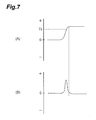
- FIG. 7(A) whose ordinate and abscissa indicate the total light quantity detected by the four-divided position detecting device of the light-receiving part 45 (see FIG. 1 )
- FIG. 8(A) whose ordinate and abscissa indicate the total light quantity detected by the four-divided position detecting device of the light-receiving part 45 (see FIG. 1 )
- FIG. 1 is a chart recording the change in the total light quantity detected by the four-divided position detecting device of the light-receiving part 45 (see FIG. 1 ) in the states of FIGS. 6(B) and 6(C) .
- the processing objective lens 42 is located at a position corresponding to one end of the line to cut C 1 at the time when the light quantity becomes smaller than a predetermined threshold T 2 .
- the amount of expansion/contraction of the actuator 43 is stored in the circular memory 706 (see FIG. 2 ) during period G (in the case where the amount of expansion/contraction of the actuator 43 is fixed at the time when the total light quantity becomes smaller than the threshold T 2 ) or period H (in the case where the amount of expansion/contraction of the actuator 43 is fixed at the time when the amount of change in the total light quantity attains a negative peak) in FIG. 8(A) .
- the circular memory comprises 64 channels, an average value of the amounts of expansion/contraction of the actuator 43 stored in the first 5 channels of the memory may be determined, for example, and the amount of expansion/contraction of the actuator 43 may be fixed so as to become thus determined average value.
- the actuator 43 is fixed at a position corresponding to the main surface height of the object corresponding to the initial quarter of the period G or H in FIG. 8(A) , which is more suitably set as the initial position for the next line to cut C 2 .
- the laser emission controller 701 of the control unit 7 outputs control signals to the laser head 13 and laser diode 44 so as to make them emit the processing laser beam L 1 and the rangefinding laser beam L 2 , respectively (step S 11 ). In response to the output of the control signals, the processing laser beam L 1 and the rangefinding laser beam L 2 are emitted.
- the stage controller 702 of the control unit 7 outputs a control signal to the stage 2 so as to move the processing objective lens 42 in the direction of arrow E in FIG. 6(A) (step S 12 ). In response to the output of this control signal, the stage 2 starts moving.
- the end part determiner 705 of the control unit 7 determines whether the processing objective lens 42 is located at an end part of the object S or not (step S 13 ).
- the end part determiner 705 outputs an instruction signal to the actuator controller 703 so as to make the latter start the expansion/contraction of the actuator 43 such that the astigmatism signal equals the held reference value.
- the actuator controller 703 outputs the control signal to the actuator 43 so as to make the latter start expanding/contracting in order for the astigmatism signal to equal the held reference value (step S 14 ).
- the actuator 43 expands/contracts according to the displacement of the surface S 1 of the object S, and holds the processing objective lens 42 such that the converging point of the rangefinding laser beam L 2 is located at the reference position. Therefore, the modified region R is formed at a position corresponding to the displacement of the surface S 1 of the object S (see FIG. 6(B) ).
- the end part determiner 705 determines whether the processing objective lens 42 is located at the other end part of the object S or not (step S 15 ). When it is determined that the processing objective lens 42 is located at the end part of the object S, the end part determiner 705 outputs an instruction signal to the actuator controller 703 so as to make the latter stop the expansion/contraction of the actuator 43 . In response to the output of this instruction signal, the actuator controller 703 outputs a control signal to the actuator 43 so as to make the latter stop expanding/contracting and attain a held state (step S 16 ). In response to the output of this control signal, the actuator 43 stops expanding/contracting.
- the stage movement controller 702 When the processing objective lens 42 is located at the point X 2 on an extension of the line to cut C 1 , the stage movement controller 702 outputs a control signal to the stage 2 so as to make the latter stop moving (step S 17 ). Thereafter, an average value of the amounts of expansion/contraction of the actuator 43 stored in the first 5 channels of the circular memory 706 among the amounts of expansion/contraction of the actuator 43 stored in the circular memory 706 is calculated, and the amount of expansion/contraction of the actuator 43 is fixed so as to become this average value (step S 18 ).
- the above-mentioned preparatory step and processing step are performed for all the lines to cut C 1 to C n , in the object S, whereby respective modified regions R are formed along the lines to cut C 1 to C n .
- this embodiment starts laser processing by emitting the processing laser beam L 1 while holding the processing objective lens 42 at the initial position, the influence of fluctuations in the shape of end parts in the object S can be excluded as much as possible.
- the processing objective lens 42 After forming a modified region in an end part of the object S while holding the processing objective lens 42 at the initial position, the processing objective lens 42 is released from being held, and then the modified region is formed while adjusting the distance between the processing objective lens 42 and the object S to a fixed value, whereby the modified region can stably be formed at a position separated by a predetermined distance from the surface S 1 of the object S.
- the processing objective lens 42 is held so as to be kept from being driven toward the main surface S 1 of the object S, whereby a smooth transition is possible when shifting to the processing of the next line to cut.
- the position of the processing objective lens 42 with respect to the main surface S 1 is set to the position based on the amount of expansion/contraction of the actuator 43 stored before a predetermined time from the time when the processing objective lens 42 is held so as to be kept from being driven, the influence of fluctuations in the shape of end parts in the object S can be excluded as much as possible.
- the modified region can stably be formed along the line to cut, when cutting/separating a wafer, which is an object to be processed, into chips by expanding the dicing film 2 a and so forth after forming the modified region, the wafer can always be cut stably with a favorable cutting quality even when cutting a large amount of wafer.
- the laser processing method and laser processing apparatus of the present invention can efficiently carry out laser processing while minimizing the deviation of the converging point of a laser beam in end parts of an object to be processed.
Abstract
A laser processing method which can efficiently perform laser processing while minimizing the deviation of the converging point of a laser beam in end parts of an object to be processed is provided. This laser processing method comprises a preparatory step of holding a lens at an initial position set such that a converging point is located at a predetermined position within the object; a first processing step (S 11 and S 12) of emitting a first laser beam for processing while holding the lens at the initial position, and moving the lens and the object relative to each other along a main surface so as to form a modified region in one end part of a line to cut; and a second processing step (S13 and S14) of releasing the lens from being held at the initial position after forming the modified region in the one end part of the line to cut, and then moving the lens and the object relative to each other along the main surface while adjusting the gap between the lens and the main surface after the release, so as to form the modified region.
Description
This is a continuation application of copending application Ser. No. 10/585,343 filed on May 7, 2008, which is a national stage application of PCT Application No. PCT/JP2004/018594 filed on Dec. 13, 2004, designating the U.S.A., the entire contents of each of which are incorporated by reference herein in their entirety.
The present invention relates to a laser processing method and laser processing apparatus for processing an object to be processed by irradiating the object with a laser beam.
Known as a conventional laser processing technique is one in which measurement means (a contact-type displacement meter, an ultrasonic rangefinder, or the like) for measuring the main surface height of the object to be processed is arranged in parallel with a condenser lens for converging a laser beam with a predetermined gap therebetween (see, for example, FIGS. 6 to 10 of Patent Document 1). In such a laser processing technique, while scanning the object with the laser beam along its main surface, the main surface height of the object is measured by the measurement means, and the condenser lens is driven along its optical axis such that the distance between the condenser lens and the main surface of the object becomes constant according to thus measured main surface at the time when the measurement point is positioned directly under the condenser lens.
Known as a technique for processing an object to be processed whose main surface has irregularities, on the other hand, is one in which the planarity in the whole part to be processed is measured by planarity measuring means (a planarity meter comprising a projector and a reflected light receiver) as a preparation for processing, and the object is processed according to thus measured planarity (see, for example, Patent Document 2).
- Patent Document 1: Japanese Patent Application Laid-Open No. 2002-219591
- Patent Document 2: Japanese Patent Application Laid-Open No. HEI 11-345785
However, the following problem to be overcome exists in the above-mentioned laser processing apparatus disclosed in Patent Document 1. When the laser beam irradiation is started from a position on the outside of the object to be processed, so as to perform processing while the laser beam and the object are moved along the main surface of the latter, the measurement means proceeds with measurement from the outside of the object to the inside thereof. When the condenser lens is driven according to the measured value of main surface height obtained by this measurement, the converging point of the laser beam may deviate from its predetermined position in end parts of the object to be processed.
Though the planarity of the main surface of the object to be processed can accurately be grasped when the technique disclosed in Patent Document 2 is used, the same part must be scanned twice, i.e., before and during the actual processing, which takes time and lowers the processing efficiency.
Therefore, it is an object of the present invention to provide a laser processing method and laser processing apparatus which can efficiently perform laser processing while minimizing the deviation of the laser beam converging point in the end parts of the object.
The inventors conducted various studies in order to overcome the above-mentioned problem. First, a processing method in which a first laser beam for processing and a second laser beam for measuring the displacement of a main surface of an object to be processed are emitted to the object on the same axis was studied. Details of this study will now be explained with reference to FIGS. 10(A) to 10(C) .
As the silicon wafer 800 shifts in the direction of arrow A in FIG. 10(A) , the optical axis of the first laser beam 806 and second laser beam 808 reaches a position where it intersects the silicon wafer 800. The piezoelectric actuator 804 c causes the lens holder 804 b to advance/retract with respect to the silicon wafer 800 such that an astigmatism signal detected from reflected light of the second laser beam 808 becomes a predetermined value. Therefore, the piezoelectric actuator 804 c retracts from the state of FIG. 10(B) , so as to raise the lens holder 804 b and condenser lens 804 a. However, since the silicon wafer 800 keeps shifting in the direction of arrow A in FIG. 10(A) , a time lag occurs until the lens holder 804 b and condenser lens 804 a rise to a predetermined position so that the converging point of the first laser beam 806 is positioned at the line to cut 800 a. Also, the astigmatism signal may vary so much that the converging point of the first laser beam 806 fluctuates.
Therefore, as shown in FIG. 10(C) , a part other than the line to cut 800 a is processed with the laser in an area B until the first laser beam 806 is in focus with the line to cut 800 a so as to attain a stable state. For example, assuming that the silicon wafer 800 has a thickness of 100 μm, and that a time delay of 15 mS occurs, the length of the area B is theoretically 1.5 mm when the processing speed is 100 mm/S.
Though FIGS. 10(A) to 10(C) relate to the silicon wafer 800 having an ideally high planarity, there may be a case where end parts are warped upward. An example of a silicon wafer having an end part warped upward will be explained with reference to FIGS. 11(A) to 11(C) .
As the silicon wafer 810 shifts in the direction of arrow A in FIG. 11(A) , the optical axis of the first laser beam 806 and second laser beam 808 reaches a position where it intersects the silicon wafer 810 as shown in FIG. 11(B) . The piezoelectric actuator 804 c causes the lens holder 804 b to advance/retract with respect to the silicon wafer 810 such that an astigmatism signal detected from reflected light of the second laser beam 808 becomes a predetermined value. Therefore, the piezoelectric actuator 804 c retracts from the state of FIG. 11(B) , so as to raise the lens holder 804 b and condenser lens 804 a. However, since the silicon wafer 810 keeps shifting in the direction of arrow A in FIG. 11(A) , a time lag occurs until the lens holder 804 b and condenser lens 804 a rise to a predetermined position so that the converging point of the first laser beam 806 is positioned at the line to cut 810 a. Also, since an end part of the silicon wafer 810 is warped upward, the gap from the position of the dotted line C to the actual position of the main surface 810 b in FIG. 11(B) causes an overshoot when the lens holder 804 b and condenser lens 804 a rise to the predetermined position.
Therefore, as shown in FIG. 11(C) , a part other than the line to cut 810 a is processed with the laser in an area D until the first laser beam 806 is in focus with the line to cut 810 a so as to attain a stable state. The length of the area D tends to be longer by the overshoot than the length of the area B in FIG. 10(C) . Hence, the inventors take notice of the processing in end parts of the object to be processed. The present invention is achieved according to these findings.
The present invention provides a laser processing method for irradiating an object to be processed with a first laser beam while converging the first laser beam with a lens such that a converging point is positioned within the object, and forming a modified region within the object along a line to cut in the object; the method comprising a preparatory step of holding the lens at an initial position with respect to a main surface of the object, the initial position being set so that the converging point is located at a predetermined position within the object; a first processing step of emitting the first laser beam while holding the lens at the initial position, and moving the lens and the object relative to each other along the main surface so as to form the modified region in one end part of the line to cut; and a second processing step of releasing the lens from being held at the initial position after forming the modified region in the one end part, and then moving the lens and the object relative to each other along the main surface while adjusting a gap between the lens and the main surface so as to form the modified region.
Since the modified region is formed in one end part of the line to cut while the lens is held at the initial position, the modified region can be formed while excluding the influence of fluctuations in the shape of end parts in the object as much as possible in the laser processing method of the present invention. After the modified region is formed in one end part of the line to cut, the lens is released from being held, and the modified region is formed in the remaining part while adjusting the lens position, whereby the modified region can be formed at a predetermined position within the object.
It will be preferred in the laser processing method of the present invention if, in the second processing step, the first laser beam and a second laser beam for measuring a displacement of the main surface are converged by the lens onto the object on the same axis, and the lens is released from being held after the quantity of reflected light of the second laser beam reflected by the main surface exceeds a predetermined threshold. Since the first and second laser beams are converged by the lens so as to be emitted on the same axis, the converging point of the first laser beam can be prevented from deviating from a predetermined position within the object because of a vibration of a stage mounting the object, for example. The quantity of reflected light varies depending on the distance from the reflecting surface. Therefore, when a predetermined threshold is set to a value corresponding to the height of the main surface, and a location where the quantity of reflected light becomes the predetermined threshold is assumed to correspond to an outer edge of the main surface of the object to be processed, the lens can be released from being held.
It will also be preferred in the laser processing method of the present invention if, in the second processing step, the first laser beam and a second laser beam for measuring a displacement of the main surface are converged by the lens onto the object on the same axis, and the lens is released from being held after an amount of change in the quantity of reflected light of the second laser beam reflected by the main surface becomes a maximum value. Since the first and second laser beams are converged by the lens so as to be emitted on the same axis, the converging point of the first laser beam can be prevented from deviating from a predetermined position within the object because of a vibration of a stage mounting the object, for example. Since the quantity of reflected light varies depending on the distance from the reflecting surface, the displacement of the main surface seems to be acute in the vicinity of the location where the amount of change in the quantity of reflected light becomes an extreme value. Therefore, assuming that this location corresponds to an outer edge of the main surface of the object to be processed, the lens can be released from being held.
It will also be preferred if the laser processing method of the present invention further comprises a transition step of holding the lens so as to keep the lens from being driven toward the main surface after the second processing step. Since the lens is held so as not to be driven toward the main surface after forming the modified region, a smooth transition is possible when shifting to the processing of the next line to cut, for example.
It will also be preferred in the laser processing method of the present invention if, in the transition step, the first laser beam and a second laser beam for measuring a displacement of the main surface are converged by the lens onto the object on the same axis, and the lens is held so as to be kept from being driven after the quantity of reflected light of the second laser beam reflected by the main surface becomes smaller than a predetermined threshold. The quantity of reflected light varies depending on the distance from the reflecting surface. Therefore, when a predetermined threshold is set to a value corresponding to the height of the main surface, and a location where the quantity of reflected light becomes the predetermined threshold is assumed to correspond to an outer edge of the main surface of the object to be processed, the lens can be held so as to be kept from being driven.
It will also be preferred in the laser processing method of the present invention if, in the transition step, the first laser beam and a second laser beam for measuring a displacement of the main surface are converged by the lens onto the object on the same axis, and the lens is held so as to be kept from being driven after an amount of change in the quantity of reflected light of the second laser beam reflected by the main surface becomes a minimum value. Since the quantity of reflected light varies depending on the distance from the reflecting surface, the displacement of the main surface seems to be acute in the vicinity of the location where the amount of change in the quantity of reflected light becomes a minimum value. Therefore, assuming that this location corresponds to an outer edge of the main surface of the object to be processed, the lens can be held so as to be kept from being driven.
It will also be preferred in the laser processing method of the present invention if the line to cut includes first and second lines to cut; respective displacements of the main surface in unit time zones are successively stored in the second processing step of the first line to cut; the lens is held in the transition step of the first line to cut such that, with respect to the main surface, the lens is placed at a position based on the displacement stored in the unit time zone earlier by a predetermined number than the unit time zone where the lens is held so as to be kept from being driven in the transition step of the first line to cut; and the position where the lens is held in the transition step of the first line to cut is employed as the initial position in the preparatory step of the second line to cut. Since the position of the lens with respect to the main surface in the preparatory step of the next line to cut is set to the position based on the displacement stored in the unit time zone earlier by a predetermined number than the unit time zone corresponding to the time when the lens is held so as to be kept from being driven, the influence of fluctuations in the shape of end parts can be excluded as much as possible.
The present invention provides a laser processing apparatus for irradiating an object to be processed with a first laser beam while converging the first laser beam with a lens such that a converging point is positioned within the object, and forming a modified region within the object along a line to cut in the object; the apparatus comprising a lens for converging the first laser beam onto the object; moving means for moving the object and the lens relative to each other along a main surface of the object; holding means for holding the lens such that the lens freely advances and retracts with respect to the main surface; and control means for controlling respective behaviors of the moving means and holding means; wherein the control means controls the holding means so as to hold the lens at an initial position where the converging point is located at a predetermined position within the object; wherein, while emitting the first laser beam with the lens being held at the initial position, the control means controls the moving means so as to move the object and the lens relative to each other along the main surface, thereby forming the modified region in one end part of the line to cut; and wherein, after forming the modified region in the one end part of the line to cut, the control means controls the holding means so as to release the lens from being held at the initial position and hold the lens while adjusting a gap between the lens and the main surface, and controls the moving means so as to move the lens and the object relative to each other along the main surface, thereby forming the modified region.
Since the modified region is formed in one end part of the line to cut while the lens is held at the initial position, the laser processing apparatus of the present invention can form the modified region while excluding the influence of fluctuations in the shape of end parts in the object as much as possible. After the modified region is formed at one end part of the line to cut, the lens is released from being held, and the modified region is formed in the remaining part while adjusting the lens position, whereby the modified region can be formed at a predetermined position within the object.
It will be preferred in the laser processing apparatus of the present invention if the first laser beam and a second laser beam for measuring a displacement of the main surface are converged by the lens onto the object on the same axis, and the control means controls the holding means so as to release the lens from being held after the quantity of reflected light of the second laser beam reflected by the main surface exceeds a predetermined threshold. Since the first and second laser beams are converged by the lens so as to be emitted on the same axis, the converging point of the first laser beam can be prevented from deviating from a predetermined position within the object because of a vibration of a stage mounting the object, for example. The quantity of reflected light varies depending on the distance from the reflecting surface. Therefore, when a predetermined threshold is set to a value corresponding to the height of the main surface, and a location where the quantity of reflected light becomes the predetermined threshold is assumed to correspond to an outer edge of the main surface of the object to be processed, the lens can be released from being held.
It will also be preferred in the laser processing apparatus of the present invention if the first laser beam and a second laser beam for measuring a displacement of the main surface are converged by the lens onto the object on the same axis, and the control means controls the holding means so as to release the lens from being held after an amount of change in the quantity of reflected light of the second laser beam reflected by the main surface becomes a maximum value. Since the first and second laser beams are converged by the lens so as to be emitted on the same axis, the converging point of the first laser beam can be prevented from deviating from a predetermined position within the object because of a vibration of a stage mounting the object, for example. Since the quantity of reflected light varies depending on the distance from the reflecting surface, the displacement of the main surface seems to be acute in the vicinity of the location where the amount of change in the quantity of reflected light becomes an extreme value. Therefore, assuming that this location corresponds to an outer edge of the main surface of the object to be processed, the lens can be released from being held.
It will also be preferred in the laser processing apparatus of the present invention if, after forming the modified region in the one end part of the line to cut, the control means controls the holding means so as to release the lens from being held at the initial position and hold the lens while adjusting a gap between the lens and the main surface, and controls the moving means so as to move the lens and the object relative to each other along the main surface, thereby forming the modified region; and the control means controls the holding means so as to hold the lens such that the lens is kept from being driven toward the main surface and move the lens and the object relative to each other along the main surface. Since the lens is held so as not to be driven toward the main surface after forming the modified region, a smooth transition is possible when shifting to the processing of the next line to cut, for example.
It will also be preferred in the laser processing apparatus of the present invention if the first laser beam and a second laser beam for measuring a displacement of the main surface are converged by the lens onto the object on the same axis, and the control means controls the holding means so as to hold the lens such that the lens is kept from being driven toward the main surface after the quantity of reflected light of the second laser beam reflected by the main surface becomes smaller than a predetermined threshold. The quantity of reflected light varies depending on the distance from the reflecting surface. Therefore, when a predetermined threshold is set to a value corresponding to the height of the main surface, and a location where the quantity of reflected light becomes the predetermined threshold is assumed to correspond to an outer edge of the main surface of the object to be processed, the lens can be held so as to be kept from being driven.
It will also be preferred in the laser processing apparatus of the present invention if the first laser beam and a second laser beam for measuring a displacement of the main surface are converged by the lens onto the object on the same axis, and the control means controls the holding means so as to hold the lens such that the lens is kept from being driven toward the main surface after an amount of change in the quantity of reflected light of the second laser beam reflected by the main surface becomes a minimum value. Since the quantity of reflected light varies depending on the distance from the reflecting surface, the displacement of the main surface seems to be acute in the vicinity of the location where the amount of change in the quantity of reflected light becomes a minimum value. Therefore, assuming that this location corresponds to an outer edge of the main surface of the object to be processed, the lens can be held so as to be kept from being driven.
It will also be preferred in the laser processing apparatus of the present invention if the line to cut includes first and second lines to cut, the apparatus further comprises displacement storage means for successively storing respective displacements of the main surface in unit time zones, and the control means sets a position based on the displacement stored in the unit time zone earlier by a predetermined number than the unit time zone where the lens is held so as to be kept from being driven in the first line to cut as the initial position in the second line to cut. Since the position of the lens with respect to the main surface in the preparatory step of the next line to cut is set to the position based on the displacement stored in the unit time zone earlier by a predetermined number than the unit time zone corresponding to the time when the lens is held so as to be kept from being driven, the influence of fluctuations in the shape of end parts can be excluded as much as possible.
The laser processing method and laser processing apparatus of the present invention can efficiently carry out laser processing while minimizing the deviation of the converging point of a laser beam in end parts of an object to be processed.
1 . . . laser processing apparatus, 2 . . . stage, 3 . . . laser head unit, 4 . . . optical system main part, 5 . . . objective lens unit, 6 . . . laser emitting apparatus, 7 . . . control unit, S . . . object, R . . . modified region, 42 . . . processing objective lens, 43 . . . actuator, 13 . . . laser head, 44 . . . laser diode, 45 . . . light-receiving part.
Best Modes For Carrying Out The Invention
The findings of the present invention can easily be understood in view of the following detailed descriptions with reference to the accompanying drawings, which are represented for the purpose of illustration only. Embodiments of the present invention will now be explained with reference to the accompanying drawings. When possible, parts identical to each other will be referred to with numerals identical to each other without repeating their overlapping explanations.
The laser processing apparatus in accordance with an embodiment of the present invention will be explained with reference to FIG. 1 . As shown in FIG. 1 , this laser processing apparatus 1 is one which irradiates a planar object to be processed S mounted on a stage 2 (moving means) with a processing laser beam L1 (first laser beam) such that a converging point P is positioned within the object S, so as to form a modified region R caused by multiphoton absorption within the object S. The stage 2 is movable upward/downward and leftward/rightward and rotatable, whereas a laser emitting apparatus 6 mainly constituted by a laser head unit 3, an optical system main part 4, and an objective lens unit 5 is disposed above the stage 2. The laser processing apparatus 1 also comprises a control unit 7 (control means), which outputs control signals for controlling behaviors of the stage 2 and laser emitting apparatus 6 (the movement of stage 2, emission of laser beams from the laser emitting apparatus 6, etc.) thereto.
The laser head unit 3 is detachably attached to an upper end part of the optical system main part 4. The laser head unit 3 includes an L-shaped cooling jacket 11. Embedded in a vertical wall 11 a of the cooling jacket 11 is a cooling pipe 12 in a winding state, through which cooling water circulates. Attached to the front face of the vertical wall 11 a are a laser head 13 which emits the processing laser beam L1 downward, and a shutter unit 14 for selectively opening and closing an optical path of the processing laser beam L1 emitted from the laser head 13. This can prevent the laser head 13 and shutter unit 14 from overheating. For example, the laser head 13 uses an Nd:YAG laser and emits a pulsed laser beam having a pulse width of 1 μs or shorter as the processing laser beam L1.
In the laser head unit 3, an adjuster 15 for adjusting the inclination of the cooling jacket 11 and the like is attached to the lower face of a bottom wall 11 b of the cooling jacket 11. The adjuster 15 is used for aligning an optical axis α of the processing laser beam L1 emitted from the laser head 13 with an axis β which is set in the optical system main part 4 and objective lens unit 5 such as to extend vertically. Namely, the laser head unit 3 is attached to the optical system main part 4 by way of the adjuster 15. When the inclination of the cooling jacket 11 or the like is adjusted by the adjuster 15 thereafter, the inclination of the laser head 13 or the like is adjusted in conformity to the movement of the cooling jacket 11. As a consequence, the processing laser beam L1 advances into the optical system main part 4 while in a state where its optical axis α coincides with the axis β. The bottom wall 11 b of the cooling jacket 11, the adjuster 15, and a housing 21 of the optical system main part 4 are formed with through holes through which the processing laser beam L1 passes.
On the axis β within the housing 21 of the optical system main part 4, a beam expander 22 for enlarging the beam size of the processing laser beam L1 emitted from the laser head 13, an optical attenuator 23 for adjusting the output of the processing laser beam L1, an output observation optical system 24 for observing the output of the processing laser beam L1 adjusted by the optical attenuator 23, and a polarization adjusting optical system 25 for adjusting the polarization of the processing laser beam L1 are arranged in this order from the upper side to the lower side. A beam damper 26 for absorbing the eliminated laser beam is attached to the optical attenuator 23, and is connected to the cooling jacket 11 by way of a heat pipe 27. This can prevent the beam damper 26 having absorbed the laser beam from overheating.
For observing the object S mounted on the stage 2, a light guide 28 for guiding an observation visible ray is attached to the housing 21 of the optical system main part 4, whereas a CCD camera 29 is disposed within the housing 21. The observation visible ray is guided by the light guide 28 into the housing 21, successively passes through a field stop 31, a reticle 32, a dichroic mirror 33, and the like, and then is reflected by a dichroic mirror 34 disposed on the axis β. The reflected observation visible ray advances downward on the axis β and irradiates the object S. On the other hand, the processing laser beam L1 is transmitted through the dichroic mirror 34.
The reflected light beam of the observation visible ray reflected by a surface S1 of the object S advances upward on the axis β, and is reflected by the dichroic mirror 34. The light beam reflected by the dichroic mirror 34 is further reflected by the dichroic mirror 33, so as to pass through an imaging lens 35, etc., thereby entering the CCD camera 29. An image of the object S captured by the CCD camera 29 is displayed on a monitor (not depicted).
The objective lens unit 5 is detachably attached to the lower end part of the optical system main part 4. Since the objective lens unit 5 is positioned by a plurality of positioning pins with respect to the lower end part of the optical system main part 4, the axis β set in the optical system main part 4 and the axis β set in the objective lens unit 5 can easily be aligned with each other. By way of an actuator 43 (holding means) using a piezoelectric device, a processing objective lens 42 is mounted to the lower end of the housing 41 of the objective lens unit 5 while in a state where the optical axis coincides with the axis β. The housing 21 of the optical system main part 4 and the housing 41 of the objective lens unit 5 are formed with through holes through which the processing laser beam L1 passes. The peak power density of the processing laser beam L1 converged by the processing objective lens 42 is at least 1×10⁸ (W/cm2) at the converging point P.
In order to position the converging point P of the processing laser beam L1 at a predetermined depth from the surface S1 of the object S, a laser diode 44 for emitting a rangefinding laser beam L2 (second laser beam) and a light-receiving part 45 (light-receiving means) are disposed within the housing 41 of the objective lens unit 5. The rangefinding laser beam L2 is emitted from the laser diode 44, and is successively reflected by a mirror 46 and a half mirror 47, and then by a dichroic mirror 48 disposed on the axis β. The reflected rangefinding laser beam L2 advances downward on the axis β, and passes through the processing objective lens 42, thereby irradiating the surface S1 of the object S. On the other hand, the processing laser beam L1 passes through the dichroic mirror 48.
The reflected light beam of the rangefinding laser beam L2 reflected by the surface S1 of the object S reenters the processing objective lens 42, and advances upward on the axis β, so as to be reflected by the dichroic mirror 48. The reflected light beam of the rangefinding laser beam L2 reflected by the dichroic mirror 48 passes through the half mirror 47, so as to enter the light-receiving part 45, and is converged on a four-divided position detecting device (displacement acquiring means) in which a photodiode is equally divided into four. According to the converged image pattern of the reflected light beam of the rangefinding laser beam L2 converged onto the four-divided position detecting device, it can be detected where the converging point of the rangefinding laser beam L2 due to the processing objective lens 42 is positioned with respect to the surface S1 of the object S. Information about the converged image pattern of the reflected light beam of the rangefinding laser beam L2 converged on the four-divided position detecting device is outputted to the control unit 7. According to this information, the control unit 7 outputs a control signal for indicating to the actuator 43 a position for holding the processing objective lens 42.
Physically, the control unit 7 comprises an interface for exchanging signals with the stage 2 and laser emitting apparatus 6, a CPU (central processing unit), and a storage device such as memory or HDD. According to a program stored in the storage device, the CPU performs a predetermined information processing operation and outputs results of the information processing as control signals to the stage 2 and laser emitting apparatus 6.
An outline of a laser processing method carried out by thus configured laser processing apparatus 1 will now be explained. First, the object S is mounted on the stage 2, and the stage 2 is moved such that the converging point P of the processing laser beam L1 is positioned within the object S. The initial position of the stage 2 is determined by the thickness and refractive index of the object S, the numerical aperture of the processing objective lens 42, etc.
Subsequently, the processing laser beam L1 is emitted from the laser head 13, the rangefinding laser beam L2 is emitted from the laser diode 44, and the stage 2 is moved such that the processing laser beam L1 and rangefinding laser beam L2 converged by the processing objective lens 42 scan a desirable line (line to cut) of the object S. Here, the light-receiving part 45 detects the reflected light beam of the rangefinding laser beam L2, and the control unit 7 controls the actuator 43 in a feedback fashion such that the converging point P of the processing laser beam L1 is always positioned at a predetermined depth from the surface S1 of the object S, whereby the position of the processing objective lens 42 is minutely adjusted along the axis β.
Therefore, even when the surface S1 of the object S wobbles, for example, a modified region R caused by multiphoton absorption can be formed at a position located at a predetermined depth from the surface S1. Forming the linear modified region R within the planar object S as such can generate a cleavage from the linear modified region R acting as a start point, whereby the object S can be cut easily with a high precision along the linear modified region R.
The laser processing method using the laser processing apparatus 1 of this embodiment will be explained more specifically. The explanation of the laser processing method will also illustrate the movement of the laser processing apparatus 1. The laser processing method in accordance with this embodiment can be divided into a preparatory step of setting an initial position of the processing objective lens 42 with respect to the wafer-like object S, and a processing step of emitting the processing laser beam L1 so as to form a modified region. Each of the preparatory step and processing step will be explained.
(Preparatory Step) First, the preparatory step of setting the initial position of the processing objective lens 42 with respect to the wafer-like object S will be explained.
More detailed explanations will be set forth with reference to FIGS. 4(A) to 4(C) . FIGS. 4(A) to 4(C) are views showing the cross section II-II of FIG. 3 . For easier understanding, the hatching indicating the cross section is omitted in FIGS. 4(A) to 4(C) . As shown in FIG. 4(A) , the object S is attracted and secured to the stage 2 by way of a dicing film 2 a. The dicing film 2 a is secured with a dicing ring (not depicted).
As shown in FIG. 4(A) , the stage 2 moves such that the processing objective lens 42 is placed at a position corresponding to the point Q1 on the line to cut C1 in the object S. The actuator 43 holding the processing objective lens 42 is in a state expanded by 25 μm from the most contracted state. This amount of expansion, i.e., 25 μm, is set as one half of the maximum amount of expansion of the actuator 43, i.e., 50 μm. In this state, the stage 2 is moved up/down so that a reflected light beam of the observation visible ray is in focus. When a large error occurs as the stage 2 moves up and down, it will be preferred if the actuator 43 is moved to a desirable position while storing the astigmatism signal at this time, the actuator 43 is returned to the original position, the stage 2 is moved (roughly), and then the actuator 43 is minutely adjusted to a position corresponding to the stored astigmatism signal.
Subsequently, as shown in FIG. 4(B) , the stage 2 is further raised by a predetermined distance (hereinafter referred to as processing height) from the state of FIG. 4(A) , such that the distance between the surface S1 of the object S and the processing objective lens 42 is set shorter by the processing height than the distance in FIG. 4(A) . Here, assuming that the focal point of the visible range and the converging point of the laser beam coincide with each other, the processing laser beam L1 is converged at a position corresponding to the value of product of the processing height from the surface S1 and the refractive index of the object S at the laser wavelength within the object S. When the object S is a silicon wafer having a refractive index of 3.6 (at a wavelength of 1.06 μm) and a processing height of 10 μm, for example, the processing laser beam L1 is converged at a position of 3.6×10=36 μm. An astigmatism signal is obtained from the reflected light beam of the rangefinding laser beam L2 in the state shown in FIG. 4(B) , and the value of this astigmatism signal is employed as a reference value.
The stage 2 is moved as it is from the state shown in FIG. 4(B) , and attains a wait state as shown in FIG. 4(C) when the processing objective lens 42 reaches a point X1 on the extension of the line to cut C1. The position of the processing objective lens 42 with respect to the object S in the vertical direction shown in FIGS. 4(B) and 4(C) is the initial position.
Operations of the laser processing apparatus 1 in this preparatory step will be explained with reference to the flowchart shown in FIG. 5 . The stage controller 702 of the control unit 7 outputs a control signal to the stage 2 such that the processing objective lens 42 moves to the point Q1 on the C1 (step S01). In response to the output of this control signal, the stage 2 moves. Further, the actuator controller 703 of the control unit 7 outputs a control signal to the actuator 43 so as to make the latter expand by 25 μm (step S02). In response to the output of this control signal, the actuator 43 expands by 25 μm. In this state, the stage 2 is moved up/down so that the observation visible ray is in focus therewith, and a focal position of the observation visible ray is set, whereby the processing objective lens 42 and the object S attain the state explained with reference to FIG. 4(A) (step S03).
The stage movement controller 702 of the control unit 7 outputs a control signal to the stage 2 so as to make the latter rise by a predetermined processing height (e.g., 10 μm) (step S04). In response to the output of this control signal, the stage rises by 10 μm, whereby the processing objective lens 42 and the object S attain the state explained with reference to FIG. 4(B) .
The laser emission controller 701 of the control unit 7 outputs a control signal to the laser diode 44 so as to make the latter emit the rangefinding laser beam L2 (step S05). In response to the output of this control signal, the laser diode 44 emits the rangefinding laser beam L2, whereas its reflected light beam reflected by the surface S1 of the object S is received by the four-divided position detecting device in the light-receiving part 45. In response to the light received, signals are outputted to the converging point calculator 704 and the end part determiner 705.
The converging point calculator 704 holds the value of astigmatism signal in this state as a reference value (step S06). Subsequently, the stage movement controller 702 outputs a control signal to the stage 2 such that the processing objective lens 42 moves to a position corresponding to X1 on an extension of the line to cut C1 in the object S (step S07). The stage 2 moves in response to the output of this control signal. When the processing objective lens 42 reaches the position corresponding to X1 on the extension of the line to cut C1 in the object S, the stage movement controller 702 outputs a control signal to the stage 2 so as to make the latter stop moving (step S08).
(Processing Step) The processing step of emitting the processing laser beam L1 and rangefinding laser beam L2 will now be explained.
The explanation will be set forth with reference to FIGS. 6(A) to 6(C) showing the cross section II-II of FIG. 3 as with FIGS. 4(A) to 4(C) . For easier understanding, the hatching indicating the cross section is omitted in FIGS. 6(A) to 6(C) . Subsequent to the state of FIG. 4(C) , FIG. 6(A) shows a state where the processing objective lens 42 has started forming a modified region on the line to cut C1. The actuator 43 is fixed at the amount of expansion set in FIG. 4(C) . The processing laser beam L1 and rangefinding laser beam L2 are emitted before the state of FIG. 6(A) after the state of FIG. 4(C) . The stage 2 moves such that the processing objective lens 42 shifts in the direction of arrow E in the drawing.
The rangefinding laser beam L2 is reflected less by the dicing film 2 a so that the total quantity of light reflected thereby is smaller, whereas the total quantity of reflected light increases in the object S. Namely, the total quantity of reflected light beam of the rangefinding laser beam L2 detected by the four-divided position detecting device in the light-receiving part 45 (see FIG. 1 ) increases, whereby it can be determined that the processing objective lens 42 is located at the position intersecting the line to cut C1 in the object S when the total quantity of reflected light beam exceeds a predetermined threshold. Therefore, when the total light quantity detected by the four-divided position detecting device in the light-receiving part 45 (see FIG. 1 ) is greater than the predetermined threshold, the processing objective lens 42 is assumed to be located at one end of the line to cut C1 (in the state corresponding to FIG. 6(A) ), the expansion amount of the actuator 43 at this time is released from being held, and the expansion amount control of the actuator 43 is started such that the astigmatism signal becomes the reference value held at step S06 at predetermined intervals (e.g., at individual sampling points). Hence, when the processing objective lens moves in the direction of arrow E in FIG. 6(A) , the state shown in FIG. 6(B) is attained. As shown in FIG. 6(B) , a modified region R is formed by a predetermined processing height in area F (one end part). After the modified region R is formed by a predetermined processing height in this area F, the processing objective lens 42 moves along the line to cut C1, and forms the modified region R with the processing laser beam L1. During this period, the actuator 43 is adjusted such that the astigmatism signal obtained from the reflected light beam of the rangefinding laser beam L2 becomes the above-mentioned reference value.
When the processing objective lens 42 further moves in the direction of arrow E in FIG. 6(A) from the state shown in FIG. 6(B) , the processing objective lens 42 is located at the other end of the line to cut C1 as shown in FIG. 6(C) . When the processing objective lens 42 reaches a position outside of the object S, a state opposite to that explained with reference to FIG. 6(A) is attained, whereby the total quantity of the reflected light beam of the rangefinding laser beam L2 detected by the four-divided position detecting device in the light-receiving part 45 (see FIG. 1 ) decreases. Therefore, when the total quantity of light detected by the four-divided position detecting device in the light-receiving part 45 (see FIG. 1 ) becomes smaller than a predetermined threshold, the processing objective lens 42 is assumed to be located at a position corresponding to one end of the line to cut C1 (in the state corresponding to FIG. 6(C) ), and the amount of expansion of the actuator at this time is held. While keeping the amount of expansion of the actuator 43, the stage 2 is moved such that the processing objective lens 42 reaches the position of X2 in FIG. 6(C) , so as to be ready for the processing of the next line to cut C2 (transition step).
Though the processing objective lens 42 having reached a position corresponding to one end of the line to cut C1 (FIG. 6(A) ) is detected according to the fact that the total light quantity detected by the four-divided position detecting device in the light-receiving part 45 (see FIG. 1 ) exceeds a predetermined threshold in the foregoing explanation, this is not restrictive, whereby other criteria may also be employed. An example of such criteria will be explained with reference to FIGS. 7(A) and 7(B) . FIG. 7(A) , whose ordinate and abscissa indicate the total light quantity detected by the four-divided position detecting device of the light-receiving part 45 (see FIG. 1 ) and time, respectively, is a chart recording the change in the total light quantity detected by the four-divided position detecting device of the light-receiving part 45 (see FIG. 1 ) in the states of FIGS. 6(A) and 6(B) . In this case, as mentioned above, it is determined that the processing objective lens 42 is located at a position corresponding to one end of the line to cut CI at the time when the light quantity exceeds a predetermined threshold T1.
From the graph of FIG. 7(A) , at predetermined intervals (e.g., at individual sampling points), the amount of change in difference obtained by subtracting the previous total light quantity value from the current total light quantity value is calculated. Thus obtained values are plotted in FIG. 7(B) whose ordinate and abscissa indicate the amount of change and time, respectively. In this case, a part exhibiting a positive peak seems to be a point where the change in the total light quantity is the largest, i.e., a part corresponding to the vicinity of the center of an edge (outer edge) of the object S. Therefore, the tracking of the actuator 43 can be started after the differential peak shown in FIG. 7(B) stops changing after the total light quantity shown in FIG. 7(A) becomes the threshold T1.
Though the processing objective lens 42 having reached a position corresponding to the other end of the line to cut C1 (FIG. 6(C) ) is detected according to the fact that the total light quantity detected by the four-divided position detecting device in the light-receiving part 45 (see FIG. 1 ) becomes smaller than a predetermined threshold in the foregoing explanation, this is not restrictive, whereby other criteria may also be employed. An example of such criteria will be explained with reference to FIGS. 8(A) and 8(B) . FIG. 8(A) , whose ordinate and abscissa indicate the total light quantity detected by the four-divided position detecting device of the light-receiving part 45 (see FIG. 1 ) and time, respectively, is a chart recording the change in the total light quantity detected by the four-divided position detecting device of the light-receiving part 45 (see FIG. 1 ) in the states of FIGS. 6(B) and 6(C) . In this case, as mentioned above, it is determined that the processing objective lens 42 is located at a position corresponding to one end of the line to cut C1 at the time when the light quantity becomes smaller than a predetermined threshold T2.
From the graph of FIG. 8(A) , at predetermined intervals (e.g., at individual sampling points), the amount of change in difference obtained by subtracting the previous total light quantity value from the current total light quantity value is calculated. Thus obtained values are plotted in FIG. 8(B) whose ordinate and abscissa indicate the amount of change and time, respectively. In this case, a part exhibiting a negative peak seems to be a point where the change in the total light quantity is the largest, i.e., a part corresponding to the vicinity of the center of an edge (outer edge) of the object S. Therefore, the amount of expansion/contraction of the actuator 43 can be fixed at that corresponding to this part.
The amount of expansion/contraction of the actuator 43 is stored in the circular memory 706 (see FIG. 2 ) during period G (in the case where the amount of expansion/contraction of the actuator 43 is fixed at the time when the total light quantity becomes smaller than the threshold T2) or period H (in the case where the amount of expansion/contraction of the actuator 43 is fixed at the time when the amount of change in the total light quantity attains a negative peak) in FIG. 8(A) . Since the circular memory comprises 64 channels, an average value of the amounts of expansion/contraction of the actuator 43 stored in the first 5 channels of the memory may be determined, for example, and the amount of expansion/contraction of the actuator 43 may be fixed so as to become thus determined average value. In this case, the actuator 43 is fixed at a position corresponding to the main surface height of the object corresponding to the initial quarter of the period G or H in FIG. 8(A) , which is more suitably set as the initial position for the next line to cut C2.
Operations of the laser processing apparatus 1 in this processing step will be explained with reference to the flowchart shown in FIG. 9 . Here, the stage 2 and processing objective lens 42 of the laser processing apparatus 1 are assumed to be in the state explained with reference to FIG. 4(C) .
The laser emission controller 701 of the control unit 7 outputs control signals to the laser head 13 and laser diode 44 so as to make them emit the processing laser beam L1 and the rangefinding laser beam L2, respectively (step S11). In response to the output of the control signals, the processing laser beam L1 and the rangefinding laser beam L2 are emitted.
The stage controller 702 of the control unit 7 outputs a control signal to the stage 2 so as to move the processing objective lens 42 in the direction of arrow E in FIG. 6(A) (step S12). In response to the output of this control signal, the stage 2 starts moving.
According to the signal outputted from the light-receiving part 45, the end part determiner 705 of the control unit 7 determines whether the processing objective lens 42 is located at an end part of the object S or not (step S13). When it is determined that the processing objective lens 42 is located at an end part of the object S, the end part determiner 705 outputs an instruction signal to the actuator controller 703 so as to make the latter start the expansion/contraction of the actuator 43 such that the astigmatism signal equals the held reference value. The actuator controller 703 outputs the control signal to the actuator 43 so as to make the latter start expanding/contracting in order for the astigmatism signal to equal the held reference value (step S14). In response to the output of this control signal, the actuator 43 expands/contracts according to the displacement of the surface S1 of the object S, and holds the processing objective lens 42 such that the converging point of the rangefinding laser beam L2 is located at the reference position. Therefore, the modified region R is formed at a position corresponding to the displacement of the surface S1 of the object S (see FIG. 6(B) ).
According to the signal outputted from the light-receiving part 45, the end part determiner 705 determines whether the processing objective lens 42 is located at the other end part of the object S or not (step S15). When it is determined that the processing objective lens 42 is located at the end part of the object S, the end part determiner 705 outputs an instruction signal to the actuator controller 703 so as to make the latter stop the expansion/contraction of the actuator 43. In response to the output of this instruction signal, the actuator controller 703 outputs a control signal to the actuator 43 so as to make the latter stop expanding/contracting and attain a held state (step S16). In response to the output of this control signal, the actuator 43 stops expanding/contracting. When the processing objective lens 42 is located at the point X2 on an extension of the line to cut C1, the stage movement controller 702 outputs a control signal to the stage 2 so as to make the latter stop moving (step S17). Thereafter, an average value of the amounts of expansion/contraction of the actuator 43 stored in the first 5 channels of the circular memory 706 among the amounts of expansion/contraction of the actuator 43 stored in the circular memory 706 is calculated, and the amount of expansion/contraction of the actuator 43 is fixed so as to become this average value (step S18).
The above-mentioned preparatory step and processing step are performed for all the lines to cut C1 to Cn, in the object S, whereby respective modified regions R are formed along the lines to cut C1 to Cn.
Since this embodiment starts laser processing by emitting the processing laser beam L1 while holding the processing objective lens 42 at the initial position, the influence of fluctuations in the shape of end parts in the object S can be excluded as much as possible.
After forming a modified region in an end part of the object S while holding the processing objective lens 42 at the initial position, the processing objective lens 42 is released from being held, and then the modified region is formed while adjusting the distance between the processing objective lens 42 and the object S to a fixed value, whereby the modified region can stably be formed at a position separated by a predetermined distance from the surface S1 of the object S.
After forming the modified region, the processing objective lens 42 is held so as to be kept from being driven toward the main surface S1 of the object S, whereby a smooth transition is possible when shifting to the processing of the next line to cut.
In the preparatory step of the next line to cut, the position of the processing objective lens 42 with respect to the main surface S1 is set to the position based on the amount of expansion/contraction of the actuator 43 stored before a predetermined time from the time when the processing objective lens 42 is held so as to be kept from being driven, the influence of fluctuations in the shape of end parts in the object S can be excluded as much as possible.
Since the modified region can stably be formed along the line to cut, when cutting/separating a wafer, which is an object to be processed, into chips by expanding the dicing film 2 a and so forth after forming the modified region, the wafer can always be cut stably with a favorable cutting quality even when cutting a large amount of wafer.
The laser processing method and laser processing apparatus of the present invention can efficiently carry out laser processing while minimizing the deviation of the converging point of a laser beam in end parts of an object to be processed.
Claims (1)
1. A laser processing method for irradiating an object to be processed with a laser beam while converging the laser beam with a lens such that a converging point is positioned within the object, and forming a modified region within the object along a horizontal cutting line in the object, the method comprising:
a preparatory step of holding the lens at an initial position with respect to a main surface of the object in a vertical direction, the initial position being set so that the converging point is located at a predetermined position within the object;
a first processing step of emitting the laser beam while prohibiting movement of the lens from the initial position in the vertical direction in response to output of an auto-focus off instruction signal prohibiting expansion/contraction of an actuator of the lens, and at the same time moving the lens and the object relative to each other along the main surface of the object, thereby forming an initial portion of the modified region in one end part of the cutting line; and
a second processing step of releasing the lens from being prohibited from moving from the initial position in the vertical direction after forming the initial portion of the modified region in the one end part in response to output of an auto-focus on instruction signal initiating allowance of expansion/contraction of an actuator of the lens, and then moving the lens and the object relative to each other along main surface while at the same time adjusting a distance of a gap between the lens and the main surface of the object, and while at the same time emitting the laser beam, thereby forming a remainder portion of the modified region in a part of the cutting line that is different than the one end part;
wherein the method switches from the first processing step to the second processing step during the forming of the modified region.
Priority Applications (3)
| Application Number | Priority Date | Filing Date | Title |
|---|---|---|---|
| US14/099,236 US9511449B2 (en) | 2004-01-09 | 2013-12-06 | Laser processing method and device |
| US15/255,926 US10293433B2 (en) | 2004-01-09 | 2016-09-02 | Laser processing method and device |
| US16/380,660 US11241757B2 (en) | 2004-01-09 | 2019-04-10 | Laser processing method and device |
Applications Claiming Priority (5)
| Application Number | Priority Date | Filing Date | Title |
|---|---|---|---|
| JP2004-004304 | 2004-01-09 | ||
| JP2004004304A JP4509578B2 (en) | 2004-01-09 | 2004-01-09 | Laser processing method and laser processing apparatus |
| PCT/JP2004/018594 WO2005065882A1 (en) | 2004-01-09 | 2004-12-13 | Laser processing method and device |
| US58534308A | 2008-05-07 | 2008-05-07 | |
| US14/099,236 US9511449B2 (en) | 2004-01-09 | 2013-12-06 | Laser processing method and device |
Related Parent Applications (2)
| Application Number | Title | Priority Date | Filing Date |
|---|---|---|---|
| PCT/JP2004/018594 Continuation WO2005065882A1 (en) | 2004-01-09 | 2004-12-13 | Laser processing method and device |
| US10/585,343 Continuation US8624153B2 (en) | 2004-01-09 | 2004-12-13 | Laser processing method and device |
Related Child Applications (1)
| Application Number | Title | Priority Date | Filing Date |
|---|---|---|---|
| US15/255,926 Division US10293433B2 (en) | 2004-01-09 | 2016-09-02 | Laser processing method and device |
Publications (2)
| Publication Number | Publication Date |
|---|---|
| US20140097163A1 US20140097163A1 (en) | 2014-04-10 |
| US9511449B2 true US9511449B2 (en) | 2016-12-06 |
Family
ID=34747111
Family Applications (4)
| Application Number | Title | Priority Date | Filing Date |
|---|---|---|---|
| US10/585,343 Active 2028-05-15 US8624153B2 (en) | 2004-01-09 | 2004-12-13 | Laser processing method and device |
| US14/099,236 Active US9511449B2 (en) | 2004-01-09 | 2013-12-06 | Laser processing method and device |
| US15/255,926 Active 2026-02-18 US10293433B2 (en) | 2004-01-09 | 2016-09-02 | Laser processing method and device |
| US16/380,660 Active 2026-04-01 US11241757B2 (en) | 2004-01-09 | 2019-04-10 | Laser processing method and device |
Family Applications Before (1)
| Application Number | Title | Priority Date | Filing Date |
|---|---|---|---|
| US10/585,343 Active 2028-05-15 US8624153B2 (en) | 2004-01-09 | 2004-12-13 | Laser processing method and device |
Family Applications After (2)
| Application Number | Title | Priority Date | Filing Date |
|---|---|---|---|
| US15/255,926 Active 2026-02-18 US10293433B2 (en) | 2004-01-09 | 2016-09-02 | Laser processing method and device |
| US16/380,660 Active 2026-04-01 US11241757B2 (en) | 2004-01-09 | 2019-04-10 | Laser processing method and device |
Country Status (10)
| Country | Link |
|---|---|
| US (4) | US8624153B2 (en) |
| EP (1) | EP1716960B1 (en) |
| JP (1) | JP4509578B2 (en) |
| KR (1) | KR101073183B1 (en) |
| CN (1) | CN100491046C (en) |
| AT (1) | ATE460247T1 (en) |
| DE (1) | DE602004025981D1 (en) |
| MY (1) | MY144645A (en) |
| TW (1) | TWI326628B (en) |
| WO (1) | WO2005065882A1 (en) |
Families Citing this family (70)
| Publication number | Priority date | Publication date | Assignee | Title |
|---|---|---|---|---|
| JP4659300B2 (en) | 2000-09-13 | 2011-03-30 | 浜松ホトニクス株式会社 | Laser processing method and semiconductor chip manufacturing method |
| TWI326626B (en) | 2002-03-12 | 2010-07-01 | Hamamatsu Photonics Kk | Laser processing method |
| ES2356817T3 (en) | 2002-03-12 | 2011-04-13 | Hamamatsu Photonics K.K. | CUTTING METHOD OF A PROCESSED OBJECT. |
| EP1494271B1 (en) | 2002-03-12 | 2011-11-16 | Hamamatsu Photonics K.K. | Method for dicing substrate |
| TWI520269B (en) | 2002-12-03 | 2016-02-01 | Hamamatsu Photonics Kk | Cutting method of semiconductor substrate |
| FR2852250B1 (en) | 2003-03-11 | 2009-07-24 | Jean Luc Jouvin | PROTECTIVE SHEATH FOR CANNULA, AN INJECTION KIT COMPRISING SUCH ANKLE AND NEEDLE EQUIPPED WITH SUCH ANKLE |
| WO2004080643A1 (en) | 2003-03-12 | 2004-09-23 | Hamamatsu Photonics K.K. | Laser beam machining method |
| ES2523432T3 (en) * | 2003-07-18 | 2014-11-25 | Hamamatsu Photonics K.K. | Cut semiconductor chip |
| JP4563097B2 (en) | 2003-09-10 | 2010-10-13 | 浜松ホトニクス株式会社 | Semiconductor substrate cutting method |
| JP4598407B2 (en) * | 2004-01-09 | 2010-12-15 | 浜松ホトニクス株式会社 | Laser processing method and laser processing apparatus |
| JP4601965B2 (en) * | 2004-01-09 | 2010-12-22 | 浜松ホトニクス株式会社 | Laser processing method and laser processing apparatus |
| JP4509578B2 (en) * | 2004-01-09 | 2010-07-21 | 浜松ホトニクス株式会社 | Laser processing method and laser processing apparatus |
| WO2005098916A1 (en) | 2004-03-30 | 2005-10-20 | Hamamatsu Photonics K.K. | Laser processing method and semiconductor chip |
| US8604383B2 (en) * | 2004-08-06 | 2013-12-10 | Hamamatsu Photonics K.K. | Laser processing method |
| JP4754801B2 (en) | 2004-10-13 | 2011-08-24 | 浜松ホトニクス株式会社 | Laser processing method |
| JP4762653B2 (en) * | 2005-09-16 | 2011-08-31 | 浜松ホトニクス株式会社 | Laser processing method and laser processing apparatus |
| JP4907965B2 (en) * | 2005-11-25 | 2012-04-04 | 浜松ホトニクス株式会社 | Laser processing method |
| JP4804911B2 (en) * | 2005-12-22 | 2011-11-02 | 浜松ホトニクス株式会社 | Laser processing equipment |
| JP4907984B2 (en) | 2005-12-27 | 2012-04-04 | 浜松ホトニクス株式会社 | Laser processing method and semiconductor chip |
| JP4781128B2 (en) * | 2006-02-24 | 2011-09-28 | 株式会社デンソー | Semiconductor wafer dicing method |
| JP4804183B2 (en) * | 2006-03-20 | 2011-11-02 | 株式会社デンソー | Semiconductor substrate dividing method and semiconductor chip manufactured by the dividing method |
| JP5183892B2 (en) | 2006-07-03 | 2013-04-17 | 浜松ホトニクス株式会社 | Laser processing method |
| US7897487B2 (en) | 2006-07-03 | 2011-03-01 | Hamamatsu Photonics K.K. | Laser processing method and chip |
| JP4813993B2 (en) * | 2006-07-05 | 2011-11-09 | 株式会社ディスコ | Wafer laser processing method |
| CN101516566B (en) * | 2006-09-19 | 2012-05-09 | 浜松光子学株式会社 | Laser processing method and laser processing apparatus |
| JP4954653B2 (en) | 2006-09-19 | 2012-06-20 | 浜松ホトニクス株式会社 | Laser processing method |
| JP5101073B2 (en) * | 2006-10-02 | 2012-12-19 | 浜松ホトニクス株式会社 | Laser processing equipment |
| JP5132911B2 (en) * | 2006-10-03 | 2013-01-30 | 浜松ホトニクス株式会社 | Laser processing method |
| JP4964554B2 (en) * | 2006-10-03 | 2012-07-04 | 浜松ホトニクス株式会社 | Laser processing method |
| WO2008041604A1 (en) * | 2006-10-04 | 2008-04-10 | Hamamatsu Photonics K.K. | Laser processing method |
| JP5336054B2 (en) * | 2007-07-18 | 2013-11-06 | 浜松ホトニクス株式会社 | Processing information supply system provided with processing information supply device |
| JP5449665B2 (en) | 2007-10-30 | 2014-03-19 | 浜松ホトニクス株式会社 | Laser processing method |
| JP5094337B2 (en) * | 2007-11-05 | 2012-12-12 | 浜松ホトニクス株式会社 | Laser processing method |
| JP5134928B2 (en) * | 2007-11-30 | 2013-01-30 | 浜松ホトニクス株式会社 | Workpiece grinding method |
| JP5054496B2 (en) * | 2007-11-30 | 2012-10-24 | 浜松ホトニクス株式会社 | Processing object cutting method |
| JP5692969B2 (en) | 2008-09-01 | 2015-04-01 | 浜松ホトニクス株式会社 | Aberration correction method, laser processing method using this aberration correction method, laser irradiation method using this aberration correction method, aberration correction apparatus, and aberration correction program |
| JP5254761B2 (en) | 2008-11-28 | 2013-08-07 | 浜松ホトニクス株式会社 | Laser processing equipment |
| JP5241525B2 (en) | 2009-01-09 | 2013-07-17 | 浜松ホトニクス株式会社 | Laser processing equipment |
| JP5241527B2 (en) | 2009-01-09 | 2013-07-17 | 浜松ホトニクス株式会社 | Laser processing equipment |
| CN102307699B (en) | 2009-02-09 | 2015-07-15 | 浜松光子学株式会社 | Workpiece cutting method |
| KR101769158B1 (en) | 2009-04-07 | 2017-08-17 | 하마마츠 포토닉스 가부시키가이샤 | Laser machining device and laser machining method |
| JP5491761B2 (en) | 2009-04-20 | 2014-05-14 | 浜松ホトニクス株式会社 | Laser processing equipment |
| DE102010009015A1 (en) * | 2010-02-24 | 2011-08-25 | OSRAM Opto Semiconductors GmbH, 93055 | Method for producing a plurality of optoelectronic semiconductor chips |
| US8722516B2 (en) | 2010-09-28 | 2014-05-13 | Hamamatsu Photonics K.K. | Laser processing method and method for manufacturing light-emitting device |
| DE102011079083A1 (en) | 2011-07-13 | 2013-01-17 | Trumpf Werkzeugmaschinen Gmbh + Co. Kg | Method for processing a workpiece and a machining device |
| US20140353005A1 (en) * | 2013-06-04 | 2014-12-04 | E I Du Pont De Nemours And Company | Method of making microwave and millimeterwave electronic circuits by laser patterning of unfired low temperature co-fired ceramic (ltcc) substrates |
| WO2015010706A1 (en) | 2013-07-23 | 2015-01-29 | Fraunhofer-Gesellschaft zur Förderung der angewandten Forschung e.V. | Method and device for separating a flat workpiece into multiple parts |
| US10509390B2 (en) | 2015-02-12 | 2019-12-17 | Glowforge Inc. | Safety and reliability guarantees for laser fabrication |
| WO2016131022A1 (en) | 2015-02-12 | 2016-08-18 | Glowforge Inc. | Cloud controlled laser fabrication |
| JP6478821B2 (en) * | 2015-06-05 | 2019-03-06 | 株式会社ディスコ | Wafer generation method |
| KR20170087610A (en) | 2016-01-21 | 2017-07-31 | 삼성전자주식회사 | Apparatus for cutting a wafer |
| JP6294378B2 (en) * | 2016-03-30 | 2018-03-14 | ファナック株式会社 | Laser processing apparatus and laser processing method provided with pre-processing control unit |
| KR102566170B1 (en) * | 2016-09-12 | 2023-08-10 | 삼성전자주식회사 | Wafer perforating device |
| WO2018098397A1 (en) | 2016-11-25 | 2018-05-31 | Glowforge Inc. | Calibration of computer-numerically-controlled machine |
| WO2018098398A1 (en) * | 2016-11-25 | 2018-05-31 | Glowforge Inc. | Preset optical components in a computer numerically controlled machine |
| JP6955893B2 (en) * | 2017-04-25 | 2021-10-27 | 株式会社ディスコ | Evaluation jig for the height position detection unit of the laser processing device and evaluation method for the height position detection unit of the laser processing device |
| JP7034621B2 (en) * | 2017-07-25 | 2022-03-14 | 浜松ホトニクス株式会社 | Laser processing equipment |
| JP6959073B2 (en) * | 2017-08-30 | 2021-11-02 | 株式会社ディスコ | Laser processing equipment |
| WO2019181063A1 (en) | 2018-03-20 | 2019-09-26 | 株式会社東京精密 | Laser machining device and laser machining method |
| JP7034551B2 (en) * | 2018-05-15 | 2022-03-14 | 株式会社ディスコ | Processing method of work piece |
| JP7120903B2 (en) | 2018-10-30 | 2022-08-17 | 浜松ホトニクス株式会社 | LASER PROCESSING APPARATUS AND LASER PROCESSING METHOD |
| US11897056B2 (en) | 2018-10-30 | 2024-02-13 | Hamamatsu Photonics K.K. | Laser processing device and laser processing method |
| US11024501B2 (en) | 2018-12-29 | 2021-06-01 | Cree, Inc. | Carrier-assisted method for parting crystalline material along laser damage region |
| US10576585B1 (en) | 2018-12-29 | 2020-03-03 | Cree, Inc. | Laser-assisted method for parting crystalline material |
| US10562130B1 (en) | 2018-12-29 | 2020-02-18 | Cree, Inc. | Laser-assisted method for parting crystalline material |
| JP7308396B2 (en) * | 2019-03-11 | 2023-07-14 | 株式会社東京精密 | LASER PROCESSING APPARATUS AND LASER PROCESSING METHOD |
| US10611052B1 (en) | 2019-05-17 | 2020-04-07 | Cree, Inc. | Silicon carbide wafers with relaxed positive bow and related methods |
| TW202116468A (en) * | 2019-07-18 | 2021-05-01 | 日商東京威力科創股份有限公司 | Processing device and processing method |
| CN113546921A (en) * | 2021-07-26 | 2021-10-26 | 贵州电网有限责任公司 | Robot and method for cleaning, derusting and passivating laser metal parts |
| CN116799110A (en) * | 2022-03-01 | 2023-09-22 | 珠海东辉半导体装备有限公司 | Method for removing and repairing Mini LED chip |
Citations (123)
| Publication number | Priority date | Publication date | Assignee | Title |
|---|---|---|---|---|
| JPS4624989Y1 (en) | 1967-08-31 | 1971-08-28 | ||
| US3629545A (en) | 1967-12-19 | 1971-12-21 | Western Electric Co | Laser substrate parting |
| US4546231A (en) | 1983-11-14 | 1985-10-08 | Group Ii Manufacturing Ltd. | Creation of a parting zone in a crystal structure |
| US4562333A (en) | 1984-09-04 | 1985-12-31 | General Electric Company | Stress assisted cutting of high temperature embrittled materials |
| US4769523A (en) | 1985-03-08 | 1988-09-06 | Nippon Kogaku K.K. | Laser processing apparatus |
| US4944922A (en) | 1986-07-04 | 1990-07-31 | Tosoh Corporation | Quantitative dispenser for a liquid |
| US5017796A (en) | 1989-01-11 | 1991-05-21 | Mitsubishi Jukogyo Kabushiki Kaisha | Moving blade tip clearance measurement apparatus and method with moveable lens |
| US5038016A (en) | 1988-11-22 | 1991-08-06 | Fiat Auto S.P.A. | Laser welding monitoring system and method |
| JPH04111800A (en) | 1990-08-31 | 1992-04-13 | Nippon Sekiei Glass Kk | Cutting work process of transparent material |
| US5122648A (en) | 1990-06-01 | 1992-06-16 | Wyko Corporation | Apparatus and method for automatically focusing an interference microscope |
| JPH04244910A (en) | 1991-01-31 | 1992-09-01 | Nec Corp | Height detection device |
| US5254833A (en) | 1991-01-11 | 1993-10-19 | Soei Tsusho Company, Ltd. | Brittle material cleavage-cutting apparatus |
| JPH06190578A (en) | 1992-12-25 | 1994-07-12 | Isuzu Motors Ltd | Laser beam machine |
| JPH06252485A (en) | 1992-12-28 | 1994-09-09 | Mitsubishi Electric Corp | Laser processing machine |
| JPH06252260A (en) | 1993-02-23 | 1994-09-09 | Tokyo Seimitsu Co Ltd | Depth measuring method of dicing trench and equipment |
| JPH0740336A (en) | 1993-07-30 | 1995-02-10 | Sumitomo Electric Ind Ltd | Diamond machining method |
| US5392110A (en) | 1992-04-22 | 1995-02-21 | Nec Corporation | Method and device for measuring height of object whose surface has irregular reflectance |
| JPH07236985A (en) | 1994-02-28 | 1995-09-12 | Mitsubishi Electric Corp | Laser beam cutting method and device therefor |
| JPH0814968B2 (en) | 1993-02-15 | 1996-02-14 | 九州日立マクセル株式会社 | Disk cleaner |
| US5543365A (en) | 1994-12-02 | 1996-08-06 | Texas Instruments Incorporated | Wafer scribe technique using laser by forming polysilicon |
| US5594235A (en) | 1993-06-17 | 1997-01-14 | Ultrapointe Corporation | Automated surface acquisition for a confocal microscope |
| US5622540A (en) | 1994-09-19 | 1997-04-22 | Corning Incorporated | Method for breaking a glass sheet |
| US5637244A (en) | 1993-05-13 | 1997-06-10 | Podarok International, Inc. | Method and apparatus for creating an image by a pulsed laser beam inside a transparent material |
| CN1160228A (en) | 1995-12-08 | 1997-09-24 | 现代电子产业株式会社 | Illumination method and apparatus for formation of micro patterns |
| JPH09260310A (en) | 1996-03-22 | 1997-10-03 | Hitachi Ltd | Electronic circuit device manufacturing method |
| US5698120A (en) | 1995-01-17 | 1997-12-16 | Mitsubishi Denki Kabushiki Kaisha | Laser machining system with control based on machining state recognition |
| JPH10163780A (en) | 1996-12-04 | 1998-06-19 | Ngk Insulators Ltd | Production of oscillator composed of piezoelectric single crystal |
| US5776220A (en) | 1994-09-19 | 1998-07-07 | Corning Incorporated | Method and apparatus for breaking brittle materials |
| JPH10202381A (en) | 1997-01-21 | 1998-08-04 | Sumitomo Electric Ind Ltd | Laser beam cutting device |
| US5826772A (en) | 1995-08-31 | 1998-10-27 | Corning Incorporated | Method and apparatus for breaking brittle materials |
| US5883356A (en) | 1996-05-13 | 1999-03-16 | Tip Engineering Group, Inc. | Laser scoring process and apparatus |
| JPH11138896A (en) | 1997-11-07 | 1999-05-25 | Sumitomo Heavy Ind Ltd | Laser marker and marking method, mark viewer and viewing method |
| JPH11163403A (en) | 1997-11-28 | 1999-06-18 | Nichia Chem Ind Ltd | Manufacture of nitride semiconductor element |
| JPH11177137A (en) | 1997-12-16 | 1999-07-02 | Nichia Chem Ind Ltd | Manufacture of nitride semiconductor element |
| US5925268A (en) | 1996-06-06 | 1999-07-20 | Engauge Inc. | Laser welding apparatus employing a tilting mechanism and seam follower |
| JPH11221684A (en) | 1998-02-06 | 1999-08-17 | Hamamatsu Photonics Kk | Pulse laser beam machine |
| JPH11267861A (en) | 1998-01-16 | 1999-10-05 | Sumitomo Heavy Ind Ltd | Marking of optical transmitting material |
| US5990944A (en) | 1996-07-19 | 1999-11-23 | Hamamatsu Photonics K.K. | Streak tube sweeping method and a device for implementing the same |
| JPH11345785A (en) | 1998-06-03 | 1999-12-14 | Hitachi Ltd | Dicing method and device |
| JP2000009991A (en) | 1998-06-19 | 2000-01-14 | Nec Corp | Device and method of automatic focusing |
| JP2000015467A (en) | 1998-07-01 | 2000-01-18 | Shin Meiwa Ind Co Ltd | Working method of workpiece by beam and its working device |
| US6055829A (en) | 1997-07-07 | 2000-05-02 | Schott Glas | Process for producing a desired breaking point on a glass body |
| JP2000219528A (en) | 1999-01-18 | 2000-08-08 | Samsung Sdi Co Ltd | Method for cutting glass substrate and device therefor |
| JP2000306865A (en) | 1999-02-17 | 2000-11-02 | Toshiba Electronic Engineering Corp | Wafer-cutting method and apparatus |
| US6175096B1 (en) | 1996-09-30 | 2001-01-16 | Force Instituttet | Method of processing a material by means of a laser beam |
| US6211488B1 (en) | 1998-12-01 | 2001-04-03 | Accudyne Display And Semiconductor Systems, Inc. | Method and apparatus for separating non-metallic substrates utilizing a laser initiated scribe |
| JP2001093864A (en) | 1999-09-24 | 2001-04-06 | Toshiba Corp | Semiconductor wafer fixing jig and method for manufacturing semiconductor device |
| US6252197B1 (en) | 1998-12-01 | 2001-06-26 | Accudyne Display And Semiconductor Systems, Inc. | Method and apparatus for separating non-metallic substrates utilizing a supplemental mechanical force applicator |
| US6257224B1 (en) | 1997-03-04 | 2001-07-10 | Ngk Insulators, Ltd. | Process for working a preform made of an oxide single crystal, and a process for producing functional devices |
| US6259058B1 (en) | 1998-12-01 | 2001-07-10 | Accudyne Display And Semiconductor Systems, Inc. | Apparatus for separating non-metallic substrates |
| US6322958B1 (en) | 1998-11-26 | 2001-11-27 | Sumitomo Heavy Industries Ltd. | Laser marking method and apparatus, and marked member |
| JP2001340979A (en) | 2000-03-30 | 2001-12-11 | Toyota Auto Body Co Ltd | Laser processing apparatus |
| US20020006765A1 (en) | 2000-05-11 | 2002-01-17 | Thomas Michel | System for cutting brittle materials |
| US6353216B1 (en) | 1996-04-25 | 2002-03-05 | Creoscitex Corporation Ltd. | Confocal measurement and diagnostic system |
| WO2002022301A1 (en) | 2000-09-13 | 2002-03-21 | Hamamatsu Photonics K.K. | Laser beam machining method and laser beam machining device |
| JP2002107120A (en) | 2000-10-02 | 2002-04-10 | Sumitomo Heavy Ind Ltd | Position detector for surface and rear, and apparatus and method for marking |
| US20020050489A1 (en) | 2000-10-26 | 2002-05-02 | Kabushiki Kaisha Toshiba | Apparatus and method for laser beam machining, and method for manufacturing semiconductor devices using laser beam machining |
| US6407360B1 (en) | 1998-08-26 | 2002-06-18 | Samsung Electronics, Co., Ltd. | Laser cutting apparatus and method |
| US6411838B1 (en) | 1998-12-23 | 2002-06-25 | Medispectra, Inc. | Systems and methods for optical examination of samples |
| US6420678B1 (en) | 1998-12-01 | 2002-07-16 | Brian L. Hoekstra | Method for separating non-metallic substrates |
| JP2002205181A (en) | 2000-09-13 | 2002-07-23 | Hamamatsu Photonics Kk | Device and method for laser beam machining |
| JP2002219591A (en) | 2001-01-22 | 2002-08-06 | Toshiba Corp | Laser beam irradiation device |
| US20020140949A1 (en) | 2001-03-30 | 2002-10-03 | Nec Corporation | Method of inspecting semiconductor integrated circuit which can quickly measure a cubic body |
| US20020153500A1 (en) | 2001-01-30 | 2002-10-24 | Fordahl Craig A. | Apparatus and method for focal point control for laser machining |
| JP2002321080A (en) | 2001-04-24 | 2002-11-05 | Tokyo Instruments Inc | Automatic focussing apparatus for laser precision processing |
| US20020170896A1 (en) | 2001-05-21 | 2002-11-21 | Samsung Electronics Co., Ltd. | Method and apparatus for cutting a non-metallic substrate using a laser beam |
| US6489588B1 (en) * | 1999-11-24 | 2002-12-03 | Applied Photonics, Inc. | Method and apparatus for separating non-metallic materials |
| JP2003002677A (en) | 2001-06-22 | 2003-01-08 | Seiko Epson Corp | Support table for laser cutting, apparatus and method for laser cutting, and method for producing liquid crystal panel |
| JP2003001457A (en) | 2000-09-13 | 2003-01-08 | Hamamatsu Photonics Kk | Laser beam machining method |
| US6580054B1 (en) | 2002-06-10 | 2003-06-17 | New Wave Research | Scribing sapphire substrates with a solid state UV laser |
| JP2003251476A (en) | 2002-03-01 | 2003-09-09 | Denso Corp | High density energy machining device and method |
| WO2004052586A1 (en) | 2002-12-06 | 2004-06-24 | Hamamatsu Photonics K.K. | Device and method for laser processing |
| US20040206882A1 (en) | 2003-04-18 | 2004-10-21 | Medispectra, Inc. | Methods and apparatus for evaluating image focus |
| JP2004337902A (en) | 2003-05-14 | 2004-12-02 | Hamamatsu Photonics Kk | Laser beam machining device and laser beam machining method |
| JP2004337903A (en) | 2003-05-14 | 2004-12-02 | Hamamatsu Photonics Kk | Laser beam machining device and laser beam machining method |
| US20050202596A1 (en) | 2002-03-12 | 2005-09-15 | Fumitsugu Fukuyo | Laser processing method |
| US20050272223A1 (en) | 2002-03-12 | 2005-12-08 | Yoshimaro Fujii | Method for dicing substrate |
| US7027155B2 (en) | 2001-03-29 | 2006-04-11 | Gsi Lumonics Corporation | Methods and systems for precisely relatively positioning a waist of a pulsed laser beam and method and system for controlling energy delivered to a target structure |
| US20060148212A1 (en) | 2002-12-03 | 2006-07-06 | Fumitsugu Fukuyo | Method for cutting semiconductor substrate |
| EP1707298A1 (en) | 2004-01-09 | 2006-10-04 | Hamamatsu Photonics K.K. | Laser processing method and device |
| EP1716960A1 (en) | 2004-01-09 | 2006-11-02 | Hamamatsu Photonics K.K. | Laser processing method and device |
| US20060255024A1 (en) | 2003-03-11 | 2006-11-16 | Fumitsufu Fukuyo | Laser beam machining method |
| US20070085099A1 (en) | 2003-09-10 | 2007-04-19 | Kenshi Fukumitsu | Semiconductor substrate cutting method |
| US20070125757A1 (en) | 2003-03-12 | 2007-06-07 | Fumitsugu Fukuyo | Laser beam machining method |
| US20070158314A1 (en) | 2003-03-12 | 2007-07-12 | Kenshi Fukumitsu | Laser processing method |
| US20070252154A1 (en) | 2003-09-11 | 2007-11-01 | Shoichi Uchiyama | Semiconductor Chip Manufacturing Method, Semiconductor Chip, Semiconductor Thin Film Chip, Electron Tube and Photo-Detecting Device |
| US20080037003A1 (en) | 2004-01-09 | 2008-02-14 | Kazuhiro Atsumi | Laser Processing Method And Device |
| US20080035611A1 (en) | 2004-08-06 | 2008-02-14 | Koji Kuno | Laser Processing Method And Semiconductor Device |
| US20090008373A1 (en) | 2005-11-25 | 2009-01-08 | Hamamatsu Photonics K.K. | Laser Processing Method |
| US20090032509A1 (en) | 2005-03-22 | 2009-02-05 | Koji Kuno | Laser Machining Method |
| US7489454B2 (en) | 2002-12-05 | 2009-02-10 | Hamamatsu Photonics K.K. | Laser processing device |
| US20090098713A1 (en) | 2007-10-12 | 2009-04-16 | Hamamatsu Photonics K.K. | Object cutting method |
| US20090107967A1 (en) | 2005-07-04 | 2009-04-30 | Hamamatsu Photonics K.K. | Method for cutting workpiece |
| US20090117712A1 (en) | 2005-08-12 | 2009-05-07 | Takeshi Sakamoto | Laser processing method |
| US20090166342A1 (en) | 2005-12-22 | 2009-07-02 | Hamamatsu Photonics K.K. | Laser Material Processing System |
| US20090166808A1 (en) | 2004-03-30 | 2009-07-02 | Takeshi Sakamoto | Laser processing method and semiconductor chip |
| US7592237B2 (en) | 2004-03-30 | 2009-09-22 | Hamamatsu Photonics K.K. | Laser processing method and object to be processed |
| US7595895B2 (en) | 2004-01-13 | 2009-09-29 | Hamamatsu Photonics K.K. | Laser beam machining system |
| US20090250446A1 (en) | 2006-09-19 | 2009-10-08 | Hamamatsu Photonics K.K. | Laser processing method and laser processing apparatus |
| US7605344B2 (en) | 2003-07-18 | 2009-10-20 | Hamamatsu Photonics K.K. | Laser beam machining method, laser beam machining apparatus, and laser beam machining product |
| US20090261083A1 (en) | 2005-09-16 | 2009-10-22 | Hamamatsu Photonics K.K. | Laser processing method and laser processing device |
| US7608214B2 (en) | 2004-10-13 | 2009-10-27 | Hamamatsu Photonics K.K. | Laser beam machining method |
| US20090302428A1 (en) | 2005-12-27 | 2009-12-10 | Hamamatsu Photonics K.K. | Laser beam machining method and semiconductor chip |
| US20100006548A1 (en) | 2006-10-03 | 2010-01-14 | Kazuhiro Atsumi | Laser working method |
| US20100009547A1 (en) | 2006-07-03 | 2010-01-14 | Hamamatsu Photonics K.K. | Laser working method |
| US20100012633A1 (en) | 2006-10-03 | 2010-01-21 | Kazuhiro Atsumi | Laser processing method |
| US20100012632A1 (en) | 2006-09-19 | 2010-01-21 | Hamamatsu Photonics K.K. | Laser processing method |
| US20100025386A1 (en) | 2006-10-02 | 2010-02-04 | Hammamatsu Photonics K.K. | Laser processing device |
| US20100032418A1 (en) | 2006-10-04 | 2010-02-11 | Hamamatsu Photonics K.K. | Laser processing method |
| US7709767B2 (en) | 2004-07-30 | 2010-05-04 | Hamamatsu Photonics K.K. | Laser processing method |
| US7718510B2 (en) | 2004-03-30 | 2010-05-18 | Hamamatsu Photonics K.K. | Laser processing method and semiconductor chip |
| US7719017B2 (en) | 2004-01-07 | 2010-05-18 | Hamamatsu Photonics K.K. | Semiconductor light-emitting device and its manufacturing method |
| US7754583B2 (en) | 2005-11-18 | 2010-07-13 | Hamamatsu Photonics K.K. | Laser processing method |
| US20100184271A1 (en) | 2006-07-03 | 2010-07-22 | Hamamatsu Photonics K.K. | Laser processing method and chip |
| US20100200550A1 (en) | 2007-10-30 | 2010-08-12 | Hamamatsu Photonics K.K. | Laser processing method |
| US20100240159A1 (en) | 2007-09-06 | 2010-09-23 | Hamamatsu Photonics K.K. | Manufacturing method of semiconductor laser element |
| US20100258539A1 (en) | 2007-07-18 | 2010-10-14 | Hamamatsu Photonics K.K. | Machining information supply equipment and supply system |
| US20100301521A1 (en) | 2007-11-30 | 2010-12-02 | Hamamatsu Photonics K.K. | Working object cutting method |
| US20100311313A1 (en) | 2007-11-30 | 2010-12-09 | Hamamatsu Photonics K.K. | Working object grinding method |
| US20110000897A1 (en) | 2007-08-03 | 2011-01-06 | Hamamatsu Photonics K.K. | Laser working method, laser working apparatus, and its manufacturing method |
| US20110001220A1 (en) | 2004-11-12 | 2011-01-06 | Hamamatsu Photonics K.K. | Laser beam machining method and semiconductor chip |
| US7939430B2 (en) | 2004-11-12 | 2011-05-10 | Hamamatsu Photonics K.K. | Laser processing method |
| US20110274128A1 (en) | 2009-01-09 | 2011-11-10 | Hamamatsu Photonics K.K. | Laser beam working machine |
Family Cites Families (11)
| Publication number | Priority date | Publication date | Assignee | Title |
|---|---|---|---|---|
| JPS53145564A (en) | 1977-05-25 | 1978-12-18 | Nec Home Electronics Ltd | Production of semiconductor device |
| JPH06100711B2 (en) | 1986-05-13 | 1994-12-12 | オリンパス光学工業株式会社 | Automatic focusing device |
| EP0554523B1 (en) * | 1992-02-03 | 1997-04-16 | Matsushita Electric Industrial Co., Ltd. | Laser beam machining apparatus and method for adjusting the height of its condenser lens |
| JPH06122084A (en) | 1992-10-14 | 1994-05-06 | Nippon Steel Corp | Method for controlling laser beam machine |
| JP3082124B2 (en) | 1994-07-05 | 2000-08-28 | 株式会社山武 | Electromagnetic flow meter |
| US5624153A (en) | 1995-09-15 | 1997-04-29 | Censullo, Jr.; Mario | Foldable chair |
| JPH10189496A (en) | 1996-12-24 | 1998-07-21 | Toshiba Corp | Method and machine for cutting wafer |
| JPH10288734A (en) | 1997-04-15 | 1998-10-27 | Nikon Corp | Automatic focusing device |
| WO2002013227A1 (en) * | 2000-07-27 | 2002-02-14 | Ebara Corporation | Sheet beam test apparatus |
| US6502381B2 (en) | 2001-04-03 | 2003-01-07 | Clark Crites | Pick-up rake |
| US7341007B2 (en) | 2003-03-05 | 2008-03-11 | Joel Vatsky | Balancing damper |
-
2004
- 2004-01-09 JP JP2004004304A patent/JP4509578B2/en not_active Expired - Lifetime
- 2004-12-13 US US10/585,343 patent/US8624153B2/en active Active
- 2004-12-13 CN CNB200480040143XA patent/CN100491046C/en active Active
- 2004-12-13 AT AT04806955T patent/ATE460247T1/en not_active IP Right Cessation
- 2004-12-13 DE DE602004025981T patent/DE602004025981D1/en active Active
- 2004-12-13 KR KR1020067014200A patent/KR101073183B1/en active IP Right Grant
- 2004-12-13 EP EP04806955A patent/EP1716960B1/en active Active
- 2004-12-13 WO PCT/JP2004/018594 patent/WO2005065882A1/en active Application Filing
-
2005
- 2005-01-04 TW TW094100124A patent/TWI326628B/en active
- 2005-01-10 MY MYPI20050077A patent/MY144645A/en unknown
-
2013
- 2013-12-06 US US14/099,236 patent/US9511449B2/en active Active
-
2016
- 2016-09-02 US US15/255,926 patent/US10293433B2/en active Active
-
2019
- 2019-04-10 US US16/380,660 patent/US11241757B2/en active Active
Patent Citations (159)
| Publication number | Priority date | Publication date | Assignee | Title |
|---|---|---|---|---|
| JPS4624989Y1 (en) | 1967-08-31 | 1971-08-28 | ||
| US3629545A (en) | 1967-12-19 | 1971-12-21 | Western Electric Co | Laser substrate parting |
| US4546231A (en) | 1983-11-14 | 1985-10-08 | Group Ii Manufacturing Ltd. | Creation of a parting zone in a crystal structure |
| US4562333A (en) | 1984-09-04 | 1985-12-31 | General Electric Company | Stress assisted cutting of high temperature embrittled materials |
| US4769523A (en) | 1985-03-08 | 1988-09-06 | Nippon Kogaku K.K. | Laser processing apparatus |
| US4944922A (en) | 1986-07-04 | 1990-07-31 | Tosoh Corporation | Quantitative dispenser for a liquid |
| US5038016A (en) | 1988-11-22 | 1991-08-06 | Fiat Auto S.P.A. | Laser welding monitoring system and method |
| US5017796A (en) | 1989-01-11 | 1991-05-21 | Mitsubishi Jukogyo Kabushiki Kaisha | Moving blade tip clearance measurement apparatus and method with moveable lens |
| US5122648A (en) | 1990-06-01 | 1992-06-16 | Wyko Corporation | Apparatus and method for automatically focusing an interference microscope |
| JPH04111800A (en) | 1990-08-31 | 1992-04-13 | Nippon Sekiei Glass Kk | Cutting work process of transparent material |
| US5254833A (en) | 1991-01-11 | 1993-10-19 | Soei Tsusho Company, Ltd. | Brittle material cleavage-cutting apparatus |
| JPH04244910A (en) | 1991-01-31 | 1992-09-01 | Nec Corp | Height detection device |
| US5392110A (en) | 1992-04-22 | 1995-02-21 | Nec Corporation | Method and device for measuring height of object whose surface has irregular reflectance |
| JPH06190578A (en) | 1992-12-25 | 1994-07-12 | Isuzu Motors Ltd | Laser beam machine |
| JPH06252485A (en) | 1992-12-28 | 1994-09-09 | Mitsubishi Electric Corp | Laser processing machine |
| US5463202A (en) | 1992-12-28 | 1995-10-31 | Mitsubishi Denki Kabushiki Kaisha | Laser machining apparatus and method |
| JPH0814968B2 (en) | 1993-02-15 | 1996-02-14 | 九州日立マクセル株式会社 | Disk cleaner |
| JPH06252260A (en) | 1993-02-23 | 1994-09-09 | Tokyo Seimitsu Co Ltd | Depth measuring method of dicing trench and equipment |
| US5637244A (en) | 1993-05-13 | 1997-06-10 | Podarok International, Inc. | Method and apparatus for creating an image by a pulsed laser beam inside a transparent material |
| US5594235A (en) | 1993-06-17 | 1997-01-14 | Ultrapointe Corporation | Automated surface acquisition for a confocal microscope |
| JPH0740336A (en) | 1993-07-30 | 1995-02-10 | Sumitomo Electric Ind Ltd | Diamond machining method |
| JPH07236985A (en) | 1994-02-28 | 1995-09-12 | Mitsubishi Electric Corp | Laser beam cutting method and device therefor |
| US5622540A (en) | 1994-09-19 | 1997-04-22 | Corning Incorporated | Method for breaking a glass sheet |
| US5776220A (en) | 1994-09-19 | 1998-07-07 | Corning Incorporated | Method and apparatus for breaking brittle materials |
| US5543365A (en) | 1994-12-02 | 1996-08-06 | Texas Instruments Incorporated | Wafer scribe technique using laser by forming polysilicon |
| US5698120A (en) | 1995-01-17 | 1997-12-16 | Mitsubishi Denki Kabushiki Kaisha | Laser machining system with control based on machining state recognition |
| US5826772A (en) | 1995-08-31 | 1998-10-27 | Corning Incorporated | Method and apparatus for breaking brittle materials |
| CN1160228A (en) | 1995-12-08 | 1997-09-24 | 现代电子产业株式会社 | Illumination method and apparatus for formation of micro patterns |
| JPH09260310A (en) | 1996-03-22 | 1997-10-03 | Hitachi Ltd | Electronic circuit device manufacturing method |
| US6353216B1 (en) | 1996-04-25 | 2002-03-05 | Creoscitex Corporation Ltd. | Confocal measurement and diagnostic system |
| US5883356A (en) | 1996-05-13 | 1999-03-16 | Tip Engineering Group, Inc. | Laser scoring process and apparatus |
| US5925268A (en) | 1996-06-06 | 1999-07-20 | Engauge Inc. | Laser welding apparatus employing a tilting mechanism and seam follower |
| US5990944A (en) | 1996-07-19 | 1999-11-23 | Hamamatsu Photonics K.K. | Streak tube sweeping method and a device for implementing the same |
| US6175096B1 (en) | 1996-09-30 | 2001-01-16 | Force Instituttet | Method of processing a material by means of a laser beam |
| JPH10163780A (en) | 1996-12-04 | 1998-06-19 | Ngk Insulators Ltd | Production of oscillator composed of piezoelectric single crystal |
| JPH10202381A (en) | 1997-01-21 | 1998-08-04 | Sumitomo Electric Ind Ltd | Laser beam cutting device |
| US6257224B1 (en) | 1997-03-04 | 2001-07-10 | Ngk Insulators, Ltd. | Process for working a preform made of an oxide single crystal, and a process for producing functional devices |
| US6055829A (en) | 1997-07-07 | 2000-05-02 | Schott Glas | Process for producing a desired breaking point on a glass body |
| JPH11138896A (en) | 1997-11-07 | 1999-05-25 | Sumitomo Heavy Ind Ltd | Laser marker and marking method, mark viewer and viewing method |
| JPH11163403A (en) | 1997-11-28 | 1999-06-18 | Nichia Chem Ind Ltd | Manufacture of nitride semiconductor element |
| JPH11177137A (en) | 1997-12-16 | 1999-07-02 | Nichia Chem Ind Ltd | Manufacture of nitride semiconductor element |
| JPH11267861A (en) | 1998-01-16 | 1999-10-05 | Sumitomo Heavy Ind Ltd | Marking of optical transmitting material |
| JPH11221684A (en) | 1998-02-06 | 1999-08-17 | Hamamatsu Photonics Kk | Pulse laser beam machine |
| JPH11345785A (en) | 1998-06-03 | 1999-12-14 | Hitachi Ltd | Dicing method and device |
| JP2000009991A (en) | 1998-06-19 | 2000-01-14 | Nec Corp | Device and method of automatic focusing |
| JP2000015467A (en) | 1998-07-01 | 2000-01-18 | Shin Meiwa Ind Co Ltd | Working method of workpiece by beam and its working device |
| US20030209528A1 (en) | 1998-08-26 | 2003-11-13 | Choo Dae-Ho | Laser cutting apparatus and method |
| US20020125232A1 (en) | 1998-08-26 | 2002-09-12 | Choo Dae-Ho | Laser cutting apparatus and method |
| US6407360B1 (en) | 1998-08-26 | 2002-06-18 | Samsung Electronics, Co., Ltd. | Laser cutting apparatus and method |
| US6322958B1 (en) | 1998-11-26 | 2001-11-27 | Sumitomo Heavy Industries Ltd. | Laser marking method and apparatus, and marked member |
| US6211488B1 (en) | 1998-12-01 | 2001-04-03 | Accudyne Display And Semiconductor Systems, Inc. | Method and apparatus for separating non-metallic substrates utilizing a laser initiated scribe |
| US6252197B1 (en) | 1998-12-01 | 2001-06-26 | Accudyne Display And Semiconductor Systems, Inc. | Method and apparatus for separating non-metallic substrates utilizing a supplemental mechanical force applicator |
| US6259058B1 (en) | 1998-12-01 | 2001-07-10 | Accudyne Display And Semiconductor Systems, Inc. | Apparatus for separating non-metallic substrates |
| US6420678B1 (en) | 1998-12-01 | 2002-07-16 | Brian L. Hoekstra | Method for separating non-metallic substrates |
| US6411838B1 (en) | 1998-12-23 | 2002-06-25 | Medispectra, Inc. | Systems and methods for optical examination of samples |
| JP2000219528A (en) | 1999-01-18 | 2000-08-08 | Samsung Sdi Co Ltd | Method for cutting glass substrate and device therefor |
| JP2000306865A (en) | 1999-02-17 | 2000-11-02 | Toshiba Electronic Engineering Corp | Wafer-cutting method and apparatus |
| JP2001093864A (en) | 1999-09-24 | 2001-04-06 | Toshiba Corp | Semiconductor wafer fixing jig and method for manufacturing semiconductor device |
| US20030024909A1 (en) | 1999-11-24 | 2003-02-06 | Applied Photonics, Inc. | Method and apparatus for separating non-metallic materials |
| US6489588B1 (en) * | 1999-11-24 | 2002-12-03 | Applied Photonics, Inc. | Method and apparatus for separating non-metallic materials |
| JP2001340979A (en) | 2000-03-30 | 2001-12-11 | Toyota Auto Body Co Ltd | Laser processing apparatus |
| US20020006765A1 (en) | 2000-05-11 | 2002-01-17 | Thomas Michel | System for cutting brittle materials |
| EP1338371A1 (en) | 2000-09-13 | 2003-08-27 | Hamamatsu Photonics K. K. | Laser beam machining method and laser beam machining device |
| US20110037149A1 (en) | 2000-09-13 | 2011-02-17 | Hamamatsu Photonics K.K. | Method of cutting a wafer-like object and semiconductor chip |
| US20100176100A1 (en) | 2000-09-13 | 2010-07-15 | Hamamatsu Photonics K.K. | Laser processing method and laser processing apparatus |
| US20100055876A1 (en) | 2000-09-13 | 2010-03-04 | Hamamatsu Photonics K.K. | Laser processing method and laser processing apparatus |
| US7626137B2 (en) | 2000-09-13 | 2009-12-01 | Hamamatsu Photonics K.K. | Laser cutting by forming a modified region within an object and generating fractures |
| US7825350B2 (en) | 2000-09-13 | 2010-11-02 | Hamamatsu Photonics K.K. | Laser processing method and laser processing apparatus |
| JP2002205181A (en) | 2000-09-13 | 2002-07-23 | Hamamatsu Photonics Kk | Device and method for laser beam machining |
| US6992026B2 (en) | 2000-09-13 | 2006-01-31 | Hamamatsu Photonics K.K. | Laser processing method and laser processing apparatus |
| JP2003001457A (en) | 2000-09-13 | 2003-01-08 | Hamamatsu Photonics Kk | Laser beam machining method |
| US7615721B2 (en) | 2000-09-13 | 2009-11-10 | Hamamatsu Photonics K.K. | Laser processing method and laser processing apparatus |
| US7547613B2 (en) | 2000-09-13 | 2009-06-16 | Hamamatsu Photonics K.K. | Laser processing method and laser processing apparatus |
| US7592238B2 (en) | 2000-09-13 | 2009-09-22 | Hamamatsu Photonics K.K. | Laser processing method and laser processing apparatus |
| US20110021004A1 (en) | 2000-09-13 | 2011-01-27 | Hamamatsu Photonics K.K. | Method of cutting a substrate, method of cutting a wafer-like object, and method of manufacturing a semiconductor device |
| WO2002022301A1 (en) | 2000-09-13 | 2002-03-21 | Hamamatsu Photonics K.K. | Laser beam machining method and laser beam machining device |
| US20040002199A1 (en) * | 2000-09-13 | 2004-01-01 | Hamamatsu Photonics K.K. | Laser processing method and laser processing apparatus |
| US7732730B2 (en) | 2000-09-13 | 2010-06-08 | Hamamatsu Photonics K.K. | Laser processing method and laser processing apparatus |
| US7396742B2 (en) | 2000-09-13 | 2008-07-08 | Hamamatsu Photonics K.K. | Laser processing method for cutting a wafer-like object by using a laser to form modified regions within the object |
| US20110027972A1 (en) | 2000-09-13 | 2011-02-03 | Hamamatsu Photonics K.K. | Method of cutting a substrate and method of manufacturing a semiconductor device |
| US20110027971A1 (en) | 2000-09-13 | 2011-02-03 | Hamamatsu Photonics K.K. | Method of cutting a substrate, method of processing a wafer-like object, and method of manufacturing a semiconductor device |
| JP2002107120A (en) | 2000-10-02 | 2002-04-10 | Sumitomo Heavy Ind Ltd | Position detector for surface and rear, and apparatus and method for marking |
| US20020050489A1 (en) | 2000-10-26 | 2002-05-02 | Kabushiki Kaisha Toshiba | Apparatus and method for laser beam machining, and method for manufacturing semiconductor devices using laser beam machining |
| JP2002219591A (en) | 2001-01-22 | 2002-08-06 | Toshiba Corp | Laser beam irradiation device |
| US20020153500A1 (en) | 2001-01-30 | 2002-10-24 | Fordahl Craig A. | Apparatus and method for focal point control for laser machining |
| US7027155B2 (en) | 2001-03-29 | 2006-04-11 | Gsi Lumonics Corporation | Methods and systems for precisely relatively positioning a waist of a pulsed laser beam and method and system for controlling energy delivered to a target structure |
| US20020140949A1 (en) | 2001-03-30 | 2002-10-03 | Nec Corporation | Method of inspecting semiconductor integrated circuit which can quickly measure a cubic body |
| JP2002321080A (en) | 2001-04-24 | 2002-11-05 | Tokyo Instruments Inc | Automatic focussing apparatus for laser precision processing |
| US20020170896A1 (en) | 2001-05-21 | 2002-11-21 | Samsung Electronics Co., Ltd. | Method and apparatus for cutting a non-metallic substrate using a laser beam |
| JP2003002677A (en) | 2001-06-22 | 2003-01-08 | Seiko Epson Corp | Support table for laser cutting, apparatus and method for laser cutting, and method for producing liquid crystal panel |
| JP2003251476A (en) | 2002-03-01 | 2003-09-09 | Denso Corp | High density energy machining device and method |
| US7749867B2 (en) | 2002-03-12 | 2010-07-06 | Hamamatsu Photonics K.K. | Method of cutting processed object |
| US20100203707A1 (en) | 2002-03-12 | 2010-08-12 | Hamamatsu Photonics K.K. | Substrate dividing method |
| US20100015783A1 (en) | 2002-03-12 | 2010-01-21 | Hamamatsu Photonics K.K. | Method of cutting an object to be processed |
| US20050272223A1 (en) | 2002-03-12 | 2005-12-08 | Yoshimaro Fujii | Method for dicing substrate |
| US20050202596A1 (en) | 2002-03-12 | 2005-09-15 | Fumitsugu Fukuyo | Laser processing method |
| US20080090382A1 (en) | 2002-03-12 | 2008-04-17 | Hamamatsu Photonics K.K. | Substrate dividing method |
| US7566635B2 (en) | 2002-03-12 | 2009-07-28 | Hamamatsu Photonics K.K. | Substrate dividing method |
| US6580054B1 (en) | 2002-06-10 | 2003-06-17 | New Wave Research | Scribing sapphire substrates with a solid state UV laser |
| US20060148212A1 (en) | 2002-12-03 | 2006-07-06 | Fumitsugu Fukuyo | Method for cutting semiconductor substrate |
| US7489454B2 (en) | 2002-12-05 | 2009-02-10 | Hamamatsu Photonics K.K. | Laser processing device |
| JP2004188422A (en) | 2002-12-06 | 2004-07-08 | Hamamatsu Photonics Kk | Device and method for machining laser beam |
| US20060144828A1 (en) | 2002-12-06 | 2006-07-06 | Kenshi Fukumitsu | Device and method for laser processing |
| WO2004052586A1 (en) | 2002-12-06 | 2004-06-24 | Hamamatsu Photonics K.K. | Device and method for laser processing |
| US20060255024A1 (en) | 2003-03-11 | 2006-11-16 | Fumitsufu Fukuyo | Laser beam machining method |
| US20070125757A1 (en) | 2003-03-12 | 2007-06-07 | Fumitsugu Fukuyo | Laser beam machining method |
| US20070158314A1 (en) | 2003-03-12 | 2007-07-12 | Kenshi Fukumitsu | Laser processing method |
| US20040206882A1 (en) | 2003-04-18 | 2004-10-21 | Medispectra, Inc. | Methods and apparatus for evaluating image focus |
| JP2004337902A (en) | 2003-05-14 | 2004-12-02 | Hamamatsu Photonics Kk | Laser beam machining device and laser beam machining method |
| JP2004337903A (en) | 2003-05-14 | 2004-12-02 | Hamamatsu Photonics Kk | Laser beam machining device and laser beam machining method |
| US20100327416A1 (en) | 2003-07-18 | 2010-12-30 | Hamamatsu Photonics K.K. | Laser beam machining method, laser beam machining apparatus, and laser beam machining product |
| US7605344B2 (en) | 2003-07-18 | 2009-10-20 | Hamamatsu Photonics K.K. | Laser beam machining method, laser beam machining apparatus, and laser beam machining product |
| US20100151202A1 (en) | 2003-07-18 | 2010-06-17 | Hamamatsu Photonics K.K. | Laser beam machining method, laser beam machining apparatus, and laser beam machining product |
| US20070085099A1 (en) | 2003-09-10 | 2007-04-19 | Kenshi Fukumitsu | Semiconductor substrate cutting method |
| US20100203678A1 (en) | 2003-09-10 | 2010-08-12 | Hamamatsu Photonics K.K. | Semiconductor substrate cutting method |
| US20070252154A1 (en) | 2003-09-11 | 2007-11-01 | Shoichi Uchiyama | Semiconductor Chip Manufacturing Method, Semiconductor Chip, Semiconductor Thin Film Chip, Electron Tube and Photo-Detecting Device |
| US7719017B2 (en) | 2004-01-07 | 2010-05-18 | Hamamatsu Photonics K.K. | Semiconductor light-emitting device and its manufacturing method |
| US20080251506A1 (en) | 2004-01-09 | 2008-10-16 | Kazuhiro Atsumi | Laser Processing Method and Device |
| EP1707298A1 (en) | 2004-01-09 | 2006-10-04 | Hamamatsu Photonics K.K. | Laser processing method and device |
| US20080037003A1 (en) | 2004-01-09 | 2008-02-14 | Kazuhiro Atsumi | Laser Processing Method And Device |
| US20080218735A1 (en) | 2004-01-09 | 2008-09-11 | Hamamatsu Photonics K.K. | Laser Processing Method And Device |
| EP1716960A1 (en) | 2004-01-09 | 2006-11-02 | Hamamatsu Photonics K.K. | Laser processing method and device |
| US7595895B2 (en) | 2004-01-13 | 2009-09-29 | Hamamatsu Photonics K.K. | Laser beam machining system |
| US7592237B2 (en) | 2004-03-30 | 2009-09-22 | Hamamatsu Photonics K.K. | Laser processing method and object to be processed |
| US20090166808A1 (en) | 2004-03-30 | 2009-07-02 | Takeshi Sakamoto | Laser processing method and semiconductor chip |
| US7718510B2 (en) | 2004-03-30 | 2010-05-18 | Hamamatsu Photonics K.K. | Laser processing method and semiconductor chip |
| US7947574B2 (en) | 2004-03-30 | 2011-05-24 | Hamamatsu Photonics K.K. | Laser processing method and semiconductor chip |
| US7709767B2 (en) | 2004-07-30 | 2010-05-04 | Hamamatsu Photonics K.K. | Laser processing method |
| US20080035611A1 (en) | 2004-08-06 | 2008-02-14 | Koji Kuno | Laser Processing Method And Semiconductor Device |
| US7608214B2 (en) | 2004-10-13 | 2009-10-27 | Hamamatsu Photonics K.K. | Laser beam machining method |
| US7939430B2 (en) | 2004-11-12 | 2011-05-10 | Hamamatsu Photonics K.K. | Laser processing method |
| US7902636B2 (en) | 2004-11-12 | 2011-03-08 | Hamamatsu Photonics K.K. | Semiconductor chip including a substrate and multilayer part |
| US20110001220A1 (en) | 2004-11-12 | 2011-01-06 | Hamamatsu Photonics K.K. | Laser beam machining method and semiconductor chip |
| US20090032509A1 (en) | 2005-03-22 | 2009-02-05 | Koji Kuno | Laser Machining Method |
| US20090107967A1 (en) | 2005-07-04 | 2009-04-30 | Hamamatsu Photonics K.K. | Method for cutting workpiece |
| US20090117712A1 (en) | 2005-08-12 | 2009-05-07 | Takeshi Sakamoto | Laser processing method |
| US20090261083A1 (en) | 2005-09-16 | 2009-10-22 | Hamamatsu Photonics K.K. | Laser processing method and laser processing device |
| US7754583B2 (en) | 2005-11-18 | 2010-07-13 | Hamamatsu Photonics K.K. | Laser processing method |
| US20100227453A1 (en) | 2005-11-18 | 2010-09-09 | Hamamatsu Photonics K.K. | Laser processing method |
| US20090008373A1 (en) | 2005-11-25 | 2009-01-08 | Hamamatsu Photonics K.K. | Laser Processing Method |
| US20090166342A1 (en) | 2005-12-22 | 2009-07-02 | Hamamatsu Photonics K.K. | Laser Material Processing System |
| US20090302428A1 (en) | 2005-12-27 | 2009-12-10 | Hamamatsu Photonics K.K. | Laser beam machining method and semiconductor chip |
| US7897487B2 (en) | 2006-07-03 | 2011-03-01 | Hamamatsu Photonics K.K. | Laser processing method and chip |
| US20100184271A1 (en) | 2006-07-03 | 2010-07-22 | Hamamatsu Photonics K.K. | Laser processing method and chip |
| US20100009547A1 (en) | 2006-07-03 | 2010-01-14 | Hamamatsu Photonics K.K. | Laser working method |
| US20100012632A1 (en) | 2006-09-19 | 2010-01-21 | Hamamatsu Photonics K.K. | Laser processing method |
| US20090250446A1 (en) | 2006-09-19 | 2009-10-08 | Hamamatsu Photonics K.K. | Laser processing method and laser processing apparatus |
| US20100025386A1 (en) | 2006-10-02 | 2010-02-04 | Hammamatsu Photonics K.K. | Laser processing device |
| US20100012633A1 (en) | 2006-10-03 | 2010-01-21 | Kazuhiro Atsumi | Laser processing method |
| US20100006548A1 (en) | 2006-10-03 | 2010-01-14 | Kazuhiro Atsumi | Laser working method |
| US20100032418A1 (en) | 2006-10-04 | 2010-02-11 | Hamamatsu Photonics K.K. | Laser processing method |
| US20100258539A1 (en) | 2007-07-18 | 2010-10-14 | Hamamatsu Photonics K.K. | Machining information supply equipment and supply system |
| US20110000897A1 (en) | 2007-08-03 | 2011-01-06 | Hamamatsu Photonics K.K. | Laser working method, laser working apparatus, and its manufacturing method |
| US20100240159A1 (en) | 2007-09-06 | 2010-09-23 | Hamamatsu Photonics K.K. | Manufacturing method of semiconductor laser element |
| US20090098713A1 (en) | 2007-10-12 | 2009-04-16 | Hamamatsu Photonics K.K. | Object cutting method |
| US20100200550A1 (en) | 2007-10-30 | 2010-08-12 | Hamamatsu Photonics K.K. | Laser processing method |
| US20100311313A1 (en) | 2007-11-30 | 2010-12-09 | Hamamatsu Photonics K.K. | Working object grinding method |
| US20100301521A1 (en) | 2007-11-30 | 2010-12-02 | Hamamatsu Photonics K.K. | Working object cutting method |
| US20110274128A1 (en) | 2009-01-09 | 2011-11-10 | Hamamatsu Photonics K.K. | Laser beam working machine |
Non-Patent Citations (25)
| Title |
|---|
| F. Fukuyo et al., "Stealth Dicing Technology for Ultra Thin Wafer", presented at 2003 ICEP (International Conference on Electronics Packaging), Apr. 16-18, 2003, Tokyo, Japan, pp. 266-269. |
| K. Hayashi, "Inner Glass Marking by Harmonics of Solid-state Laser", Proceedings of the 45th Laser Materials Processing Conference, Dec. 1998, pp. 23-28, with English abstract. |
| K. Miura et al., "Formation of Photo-induced Structures in Glasses with Femtosecond Laser," Proceedings of 42nd Laser Materials Processing Conference, Nov. 1997, pp. 105-111. |
| Office Action from related (not counterpart) U.S. Appl. No. 10/585,451 dated Apr. 20, 2011 (15 pages). |
| T. Hidetsugu, "Stealth Dicing, Its Principles and Features: A Technology Most Suitable for Dicing Very Thin Semiconductor Wafers," Electronic Material, No. 9, 2002, pp. 17-21, with English translation. |
| T. Miyazaki, "Laser Beam Machining Technology," Published by Sangyo-Tosho Inc., May 31, 1991, First Edition. pp. 9-10, with English translation. |
| T. Sano et al., "Evaluation of Processing Characteristics of Silicon with Picosecond Pulse Laser," Preprints of the National Meeting of Japan Welding Society, No. 66, Apr. 2000, pp. 72-73, with English translation. |
| T. Yajima et al., New Version Laser Handbook, published by Asakusa Shoten, Jun. 15, 1989, pp. 666-669, with English translation. |
| Tooling Machine Series, Laser Machining, published by Taiga Shuppan, Inc., Sep. 10, 1990, pp. 91-96, with English translation. |
| U.S. Appl. No. 13/061,438, filed Apr. 26, 2011. |
| U.S. Appl. No. 13/107,056, filed May 13, 2011. |
| U.S. Appl. No. 13/131,429, filed Jun. 28, 2011. |
| U.S. Appl. No. 13/143,636, filed Sep. 21, 2011. |
| U.S. Appl. No. 13/148,097, filed Aug. 26, 2011. |
| U.S. Appl. No. 13/151,877, filed Jun. 2, 2011. |
| U.S. Appl. No. 13/206,181, filed Aug. 9, 2011. |
| U.S. Appl. No. 13/213,175, filed Aug. 19, 2011. |
| U.S. Appl. No. 13/233,662, filed Sep. 15, 2011. |
| U.S. Appl. No. 13/235,936, filed Sep. 19, 2011. |
| U.S. Appl. No. 13/262,995, filed Oct. 5, 2011. |
| U.S. Appl. No. 13/265,027, filed Oct. 18, 2011. |
| U.S. Appl. No. 13/269,274, filed Oct. 7, 2011. |
| U.S. Office Action dated Apr. 14, 2011, issued in U.S. Appl. No. 10/585,660, filed May 8, 2008. |
| U.S. Office Action dated Apr. 20, 2011, issued in U.S. Appl. No. 10/585,451, filed May 4, 2007. |
| X. Liu et al., "Laser Ablation and Micromachining with Ultrashort Laser Pulses," IEEE Journal of Quantum Electronics, vol. 33, No. 10, Oct. 1997, pp. 1706-1716. |
Also Published As
| Publication number | Publication date |
|---|---|
| TW200539979A (en) | 2005-12-16 |
| US20080218735A1 (en) | 2008-09-11 |
| EP1716960A1 (en) | 2006-11-02 |
| KR101073183B1 (en) | 2011-10-12 |
| US8624153B2 (en) | 2014-01-07 |
| US20190232422A1 (en) | 2019-08-01 |
| US20140097163A1 (en) | 2014-04-10 |
| KR20070031271A (en) | 2007-03-19 |
| DE602004025981D1 (en) | 2010-04-22 |
| US20160368085A1 (en) | 2016-12-22 |
| CN100491046C (en) | 2009-05-27 |
| CN1902023A (en) | 2007-01-24 |
| JP4509578B2 (en) | 2010-07-21 |
| ATE460247T1 (en) | 2010-03-15 |
| EP1716960B1 (en) | 2010-03-10 |
| US10293433B2 (en) | 2019-05-21 |
| TWI326628B (en) | 2010-07-01 |
| JP2005193284A (en) | 2005-07-21 |
| US11241757B2 (en) | 2022-02-08 |
| WO2005065882A1 (en) | 2005-07-21 |
| MY144645A (en) | 2011-10-31 |
| EP1716960A4 (en) | 2008-08-13 |
Similar Documents
| Publication | Publication Date | Title |
|---|---|---|
| US11241757B2 (en) | Laser processing method and device | |
| EP1707298B1 (en) | Laser processing method and device | |
| US8993922B2 (en) | Laser processing method and device | |
| KR101119377B1 (en) | Laser beam machining system |
Legal Events
| Date | Code | Title | Description |
|---|---|---|---|
| STCF | Information on status: patent grant |
Free format text: PATENTED CASE |
|
| MAFP | Maintenance fee payment |
Free format text: PAYMENT OF MAINTENANCE FEE, 4TH YEAR, LARGE ENTITY (ORIGINAL EVENT CODE: M1551); ENTITY STATUS OF PATENT OWNER: LARGE ENTITY Year of fee payment: 4 |