US9515158B1 - Semiconductor structure with insertion layer and method for manufacturing the same - Google Patents
Semiconductor structure with insertion layer and method for manufacturing the same Download PDFInfo
- Publication number
- US9515158B1 US9515158B1 US14/918,054 US201514918054A US9515158B1 US 9515158 B1 US9515158 B1 US 9515158B1 US 201514918054 A US201514918054 A US 201514918054A US 9515158 B1 US9515158 B1 US 9515158B1
- Authority
- US
- United States
- Prior art keywords
- layer
- semiconductor structure
- gate dielectric
- dielectric layer
- formed over
- Prior art date
- Legal status (The legal status is an assumption and is not a legal conclusion. Google has not performed a legal analysis and makes no representation as to the accuracy of the status listed.)
- Active
Links
- 238000003780 insertion Methods 0.000 title claims abstract description 101
- 230000037431 insertion Effects 0.000 title claims abstract description 101
- 239000004065 semiconductor Substances 0.000 title claims abstract description 87
- 238000000034 method Methods 0.000 title claims abstract description 59
- 238000004519 manufacturing process Methods 0.000 title claims description 22
- 229910052751 metal Inorganic materials 0.000 claims abstract description 47
- 239000002184 metal Substances 0.000 claims abstract description 47
- QVGXLLKOCUKJST-UHFFFAOYSA-N atomic oxygen Chemical compound [O] QVGXLLKOCUKJST-UHFFFAOYSA-N 0.000 claims abstract description 36
- 229910052760 oxygen Inorganic materials 0.000 claims abstract description 36
- 239000001301 oxygen Substances 0.000 claims abstract description 36
- 239000000758 substrate Substances 0.000 claims abstract description 32
- 229910052735 hafnium Inorganic materials 0.000 claims description 8
- 229910052782 aluminium Inorganic materials 0.000 claims description 7
- 229910052684 Cerium Inorganic materials 0.000 claims description 6
- 229910052692 Dysprosium Inorganic materials 0.000 claims description 6
- 229910052691 Erbium Inorganic materials 0.000 claims description 6
- 229910052693 Europium Inorganic materials 0.000 claims description 6
- 229910052688 Gadolinium Inorganic materials 0.000 claims description 6
- 229910052689 Holmium Inorganic materials 0.000 claims description 6
- 229910052779 Neodymium Inorganic materials 0.000 claims description 6
- 229910052777 Praseodymium Inorganic materials 0.000 claims description 6
- 229910052772 Samarium Inorganic materials 0.000 claims description 6
- 229910052771 Terbium Inorganic materials 0.000 claims description 6
- 229910052775 Thulium Inorganic materials 0.000 claims description 6
- 229910052769 Ytterbium Inorganic materials 0.000 claims description 6
- 229910052746 lanthanum Inorganic materials 0.000 claims description 6
- 229910052727 yttrium Inorganic materials 0.000 claims description 6
- 239000010410 layer Substances 0.000 description 278
- 230000008569 process Effects 0.000 description 43
- 239000000463 material Substances 0.000 description 31
- 238000005229 chemical vapour deposition Methods 0.000 description 13
- 238000007789 sealing Methods 0.000 description 13
- 238000000231 atomic layer deposition Methods 0.000 description 10
- 239000003989 dielectric material Substances 0.000 description 10
- 239000011229 interlayer Substances 0.000 description 9
- VYPSYNLAJGMNEJ-UHFFFAOYSA-N Silicium dioxide Chemical compound O=[Si]=O VYPSYNLAJGMNEJ-UHFFFAOYSA-N 0.000 description 8
- 229910044991 metal oxide Inorganic materials 0.000 description 8
- 150000004706 metal oxides Chemical class 0.000 description 8
- 238000005240 physical vapour deposition Methods 0.000 description 8
- 125000006850 spacer group Chemical group 0.000 description 8
- 229910052814 silicon oxide Inorganic materials 0.000 description 7
- 229910052581 Si3N4 Inorganic materials 0.000 description 6
- XUIMIQQOPSSXEZ-UHFFFAOYSA-N Silicon Chemical compound [Si] XUIMIQQOPSSXEZ-UHFFFAOYSA-N 0.000 description 6
- 230000000295 complement effect Effects 0.000 description 6
- 229910052710 silicon Inorganic materials 0.000 description 6
- 239000010703 silicon Substances 0.000 description 6
- HQVNEWCFYHHQES-UHFFFAOYSA-N silicon nitride Chemical compound N12[Si]34N5[Si]62N3[Si]51N64 HQVNEWCFYHHQES-UHFFFAOYSA-N 0.000 description 6
- 229910045601 alloy Inorganic materials 0.000 description 4
- 239000000956 alloy Substances 0.000 description 4
- 239000011248 coating agent Substances 0.000 description 4
- 238000000576 coating method Methods 0.000 description 4
- 238000009415 formwork Methods 0.000 description 4
- 230000003647 oxidation Effects 0.000 description 4
- 238000007254 oxidation reaction Methods 0.000 description 4
- JBRZTFJDHDCESZ-UHFFFAOYSA-N AsGa Chemical compound [As]#[Ga] JBRZTFJDHDCESZ-UHFFFAOYSA-N 0.000 description 3
- 229910000530 Gallium indium arsenide Inorganic materials 0.000 description 3
- 229910000673 Indium arsenide Inorganic materials 0.000 description 3
- GPXJNWSHGFTCBW-UHFFFAOYSA-N Indium phosphide Chemical compound [In]#P GPXJNWSHGFTCBW-UHFFFAOYSA-N 0.000 description 3
- 229910000577 Silicon-germanium Inorganic materials 0.000 description 3
- 238000005137 deposition process Methods 0.000 description 3
- 238000001312 dry etching Methods 0.000 description 3
- WPYVAWXEWQSOGY-UHFFFAOYSA-N indium antimonide Chemical compound [Sb]#[In] WPYVAWXEWQSOGY-UHFFFAOYSA-N 0.000 description 3
- RPQDHPTXJYYUPQ-UHFFFAOYSA-N indium arsenide Chemical compound [In]#[As] RPQDHPTXJYYUPQ-UHFFFAOYSA-N 0.000 description 3
- 238000002955 isolation Methods 0.000 description 3
- 229910021420 polycrystalline silicon Inorganic materials 0.000 description 3
- HBMJWWWQQXIZIP-UHFFFAOYSA-N silicon carbide Chemical compound [Si+]#[C-] HBMJWWWQQXIZIP-UHFFFAOYSA-N 0.000 description 3
- 229910010271 silicon carbide Inorganic materials 0.000 description 3
- 229910005542 GaSb Inorganic materials 0.000 description 2
- 229910001218 Gallium arsenide Inorganic materials 0.000 description 2
- GWEVSGVZZGPLCZ-UHFFFAOYSA-N Titan oxide Chemical compound O=[Ti]=O GWEVSGVZZGPLCZ-UHFFFAOYSA-N 0.000 description 2
- ILCYGSITMBHYNK-UHFFFAOYSA-N [Si]=O.[Hf] Chemical compound [Si]=O.[Hf] ILCYGSITMBHYNK-UHFFFAOYSA-N 0.000 description 2
- PNEYBMLMFCGWSK-UHFFFAOYSA-N aluminium oxide Inorganic materials [O-2].[O-2].[O-2].[Al+3].[Al+3] PNEYBMLMFCGWSK-UHFFFAOYSA-N 0.000 description 2
- 239000005380 borophosphosilicate glass Substances 0.000 description 2
- 150000001875 compounds Chemical class 0.000 description 2
- 239000004020 conductor Substances 0.000 description 2
- 238000000151 deposition Methods 0.000 description 2
- 230000005684 electric field Effects 0.000 description 2
- 238000005530 etching Methods 0.000 description 2
- YBMRDBCBODYGJE-UHFFFAOYSA-N germanium dioxide Chemical compound O=[Ge]=O YBMRDBCBODYGJE-UHFFFAOYSA-N 0.000 description 2
- VBJZVLUMGGDVMO-UHFFFAOYSA-N hafnium atom Chemical compound [Hf] VBJZVLUMGGDVMO-UHFFFAOYSA-N 0.000 description 2
- ZQXQADNTSSMHJI-UHFFFAOYSA-N hafnium(4+) oxygen(2-) tantalum(5+) Chemical compound [O-2].[Ta+5].[Hf+4] ZQXQADNTSSMHJI-UHFFFAOYSA-N 0.000 description 2
- KQHQLIAOAVMAOW-UHFFFAOYSA-N hafnium(4+) oxygen(2-) zirconium(4+) Chemical compound [O--].[O--].[O--].[O--].[Zr+4].[Hf+4] KQHQLIAOAVMAOW-UHFFFAOYSA-N 0.000 description 2
- KUVFGOLWQIXGBP-UHFFFAOYSA-N hafnium(4+);oxygen(2-);titanium(4+) Chemical compound [O-2].[O-2].[O-2].[O-2].[Ti+4].[Hf+4] KUVFGOLWQIXGBP-UHFFFAOYSA-N 0.000 description 2
- CJNBYAVZURUTKZ-UHFFFAOYSA-N hafnium(iv) oxide Chemical compound O=[Hf]=O CJNBYAVZURUTKZ-UHFFFAOYSA-N 0.000 description 2
- 238000004518 low pressure chemical vapour deposition Methods 0.000 description 2
- 150000002739 metals Chemical class 0.000 description 2
- 150000004767 nitrides Chemical class 0.000 description 2
- TWNQGVIAIRXVLR-UHFFFAOYSA-N oxo(oxoalumanyloxy)alumane Chemical compound O=[Al]O[Al]=O TWNQGVIAIRXVLR-UHFFFAOYSA-N 0.000 description 2
- RVTZCBVAJQQJTK-UHFFFAOYSA-N oxygen(2-);zirconium(4+) Chemical compound [O-2].[O-2].[Zr+4] RVTZCBVAJQQJTK-UHFFFAOYSA-N 0.000 description 2
- 238000000059 patterning Methods 0.000 description 2
- 239000005360 phosphosilicate glass Substances 0.000 description 2
- 238000000623 plasma-assisted chemical vapour deposition Methods 0.000 description 2
- 238000007517 polishing process Methods 0.000 description 2
- 229920005591 polysilicon Polymers 0.000 description 2
- 230000008439 repair process Effects 0.000 description 2
- OGIDPMRJRNCKJF-UHFFFAOYSA-N titanium oxide Inorganic materials [Ti]=O OGIDPMRJRNCKJF-UHFFFAOYSA-N 0.000 description 2
- 238000001039 wet etching Methods 0.000 description 2
- 229910001928 zirconium oxide Inorganic materials 0.000 description 2
- ITWBWJFEJCHKSN-UHFFFAOYSA-N 1,4,7-triazonane Chemical compound C1CNCCNCCN1 ITWBWJFEJCHKSN-UHFFFAOYSA-N 0.000 description 1
- 229910000980 Aluminium gallium arsenide Inorganic materials 0.000 description 1
- RYGMFSIKBFXOCR-UHFFFAOYSA-N Copper Chemical compound [Cu] RYGMFSIKBFXOCR-UHFFFAOYSA-N 0.000 description 1
- 229910005540 GaP Inorganic materials 0.000 description 1
- 229910010038 TiAl Inorganic materials 0.000 description 1
- 229910010037 TiAlN Inorganic materials 0.000 description 1
- ATJFFYVFTNAWJD-UHFFFAOYSA-N Tin Chemical compound [Sn] ATJFFYVFTNAWJD-UHFFFAOYSA-N 0.000 description 1
- RTAQQCXQSZGOHL-UHFFFAOYSA-N Titanium Chemical compound [Ti] RTAQQCXQSZGOHL-UHFFFAOYSA-N 0.000 description 1
- CEPICIBPGDWCRU-UHFFFAOYSA-N [Si].[Hf] Chemical compound [Si].[Hf] CEPICIBPGDWCRU-UHFFFAOYSA-N 0.000 description 1
- 230000004075 alteration Effects 0.000 description 1
- XAGFODPZIPBFFR-UHFFFAOYSA-N aluminium Chemical compound [Al] XAGFODPZIPBFFR-UHFFFAOYSA-N 0.000 description 1
- 229910021417 amorphous silicon Inorganic materials 0.000 description 1
- 238000000137 annealing Methods 0.000 description 1
- 230000015572 biosynthetic process Effects 0.000 description 1
- 229910052681 coesite Inorganic materials 0.000 description 1
- 238000010276 construction Methods 0.000 description 1
- 229910052802 copper Inorganic materials 0.000 description 1
- 239000010949 copper Substances 0.000 description 1
- 229910052906 cristobalite Inorganic materials 0.000 description 1
- 239000013078 crystal Substances 0.000 description 1
- 229910003460 diamond Inorganic materials 0.000 description 1
- 239000010432 diamond Substances 0.000 description 1
- HZXMRANICFIONG-UHFFFAOYSA-N gallium phosphide Chemical compound [Ga]#P HZXMRANICFIONG-UHFFFAOYSA-N 0.000 description 1
- 239000007789 gas Substances 0.000 description 1
- 229910052732 germanium Inorganic materials 0.000 description 1
- GNPVGFCGXDBREM-UHFFFAOYSA-N germanium atom Chemical compound [Ge] GNPVGFCGXDBREM-UHFFFAOYSA-N 0.000 description 1
- 238000002513 implantation Methods 0.000 description 1
- 238000001459 lithography Methods 0.000 description 1
- 229910052914 metal silicate Inorganic materials 0.000 description 1
- 238000000206 photolithography Methods 0.000 description 1
- 238000005498 polishing Methods 0.000 description 1
- 239000005368 silicate glass Substances 0.000 description 1
- 239000000377 silicon dioxide Substances 0.000 description 1
- 239000002356 single layer Substances 0.000 description 1
- 229910052682 stishovite Inorganic materials 0.000 description 1
- 239000000126 substance Substances 0.000 description 1
- 238000006467 substitution reaction Methods 0.000 description 1
- 229910052715 tantalum Inorganic materials 0.000 description 1
- GUVRBAGPIYLISA-UHFFFAOYSA-N tantalum atom Chemical compound [Ta] GUVRBAGPIYLISA-UHFFFAOYSA-N 0.000 description 1
- 229910052719 titanium Inorganic materials 0.000 description 1
- 239000010936 titanium Substances 0.000 description 1
- 230000007704 transition Effects 0.000 description 1
- 229910000314 transition metal oxide Inorganic materials 0.000 description 1
- 229910000326 transition metal silicate Inorganic materials 0.000 description 1
- 229910052905 tridymite Inorganic materials 0.000 description 1
- WFKWXMTUELFFGS-UHFFFAOYSA-N tungsten Chemical compound [W] WFKWXMTUELFFGS-UHFFFAOYSA-N 0.000 description 1
- 229910052721 tungsten Inorganic materials 0.000 description 1
- 239000010937 tungsten Substances 0.000 description 1
Images


Classifications
-
- H—ELECTRICITY
- H01—ELECTRIC ELEMENTS
- H01L—SEMICONDUCTOR DEVICES NOT COVERED BY CLASS H10
- H01L29/00—Semiconductor devices adapted for rectifying, amplifying, oscillating or switching, or capacitors or resistors with at least one potential-jump barrier or surface barrier, e.g. PN junction depletion layer or carrier concentration layer; Details of semiconductor bodies or of electrodes thereof ; Multistep manufacturing processes therefor
- H01L29/40—Electrodes ; Multistep manufacturing processes therefor
- H01L29/41—Electrodes ; Multistep manufacturing processes therefor characterised by their shape, relative sizes or dispositions
- H01L29/423—Electrodes ; Multistep manufacturing processes therefor characterised by their shape, relative sizes or dispositions not carrying the current to be rectified, amplified or switched
- H01L29/42312—Gate electrodes for field effect devices
- H01L29/42316—Gate electrodes for field effect devices for field-effect transistors
- H01L29/4232—Gate electrodes for field effect devices for field-effect transistors with insulated gate
- H01L29/42364—Gate electrodes for field effect devices for field-effect transistors with insulated gate characterised by the insulating layer, e.g. thickness or uniformity
-
- H—ELECTRICITY
- H01—ELECTRIC ELEMENTS
- H01L—SEMICONDUCTOR DEVICES NOT COVERED BY CLASS H10
- H01L29/00—Semiconductor devices adapted for rectifying, amplifying, oscillating or switching, or capacitors or resistors with at least one potential-jump barrier or surface barrier, e.g. PN junction depletion layer or carrier concentration layer; Details of semiconductor bodies or of electrodes thereof ; Multistep manufacturing processes therefor
- H01L29/66—Types of semiconductor device ; Multistep manufacturing processes therefor
- H01L29/68—Types of semiconductor device ; Multistep manufacturing processes therefor controllable by only the electric current supplied, or only the electric potential applied, to an electrode which does not carry the current to be rectified, amplified or switched
- H01L29/76—Unipolar devices, e.g. field effect transistors
- H01L29/772—Field effect transistors
- H01L29/78—Field effect transistors with field effect produced by an insulated gate
- H01L29/7842—Field effect transistors with field effect produced by an insulated gate means for exerting mechanical stress on the crystal lattice of the channel region, e.g. using a flexible substrate
- H01L29/7843—Field effect transistors with field effect produced by an insulated gate means for exerting mechanical stress on the crystal lattice of the channel region, e.g. using a flexible substrate the means being an applied insulating layer
-
- H—ELECTRICITY
- H01—ELECTRIC ELEMENTS
- H01L—SEMICONDUCTOR DEVICES NOT COVERED BY CLASS H10
- H01L21/00—Processes or apparatus adapted for the manufacture or treatment of semiconductor or solid state devices or of parts thereof
- H01L21/02—Manufacture or treatment of semiconductor devices or of parts thereof
- H01L21/02104—Forming layers
- H01L21/02107—Forming insulating materials on a substrate
- H01L21/02109—Forming insulating materials on a substrate characterised by the type of layer, e.g. type of material, porous/non-porous, pre-cursors, mixtures or laminates
- H01L21/02112—Forming insulating materials on a substrate characterised by the type of layer, e.g. type of material, porous/non-porous, pre-cursors, mixtures or laminates characterised by the material of the layer
- H01L21/02172—Forming insulating materials on a substrate characterised by the type of layer, e.g. type of material, porous/non-porous, pre-cursors, mixtures or laminates characterised by the material of the layer the material containing at least one metal element, e.g. metal oxides, metal nitrides, metal oxynitrides or metal carbides
- H01L21/02175—Forming insulating materials on a substrate characterised by the type of layer, e.g. type of material, porous/non-porous, pre-cursors, mixtures or laminates characterised by the material of the layer the material containing at least one metal element, e.g. metal oxides, metal nitrides, metal oxynitrides or metal carbides characterised by the metal
- H01L21/02181—Forming insulating materials on a substrate characterised by the type of layer, e.g. type of material, porous/non-porous, pre-cursors, mixtures or laminates characterised by the material of the layer the material containing at least one metal element, e.g. metal oxides, metal nitrides, metal oxynitrides or metal carbides characterised by the metal the material containing hafnium, e.g. HfO2
-
- H—ELECTRICITY
- H01—ELECTRIC ELEMENTS
- H01L—SEMICONDUCTOR DEVICES NOT COVERED BY CLASS H10
- H01L21/00—Processes or apparatus adapted for the manufacture or treatment of semiconductor or solid state devices or of parts thereof
- H01L21/02—Manufacture or treatment of semiconductor devices or of parts thereof
- H01L21/04—Manufacture or treatment of semiconductor devices or of parts thereof the devices having at least one potential-jump barrier or surface barrier, e.g. PN junction, depletion layer or carrier concentration layer
- H01L21/18—Manufacture or treatment of semiconductor devices or of parts thereof the devices having at least one potential-jump barrier or surface barrier, e.g. PN junction, depletion layer or carrier concentration layer the devices having semiconductor bodies comprising elements of Group IV of the Periodic System or AIIIBV compounds with or without impurities, e.g. doping materials
- H01L21/28—Manufacture of electrodes on semiconductor bodies using processes or apparatus not provided for in groups H01L21/20 - H01L21/268
- H01L21/28008—Making conductor-insulator-semiconductor electrodes
- H01L21/28017—Making conductor-insulator-semiconductor electrodes the insulator being formed after the semiconductor body, the semiconductor being silicon
- H01L21/28026—Making conductor-insulator-semiconductor electrodes the insulator being formed after the semiconductor body, the semiconductor being silicon characterised by the conductor
- H01L21/28079—Making conductor-insulator-semiconductor electrodes the insulator being formed after the semiconductor body, the semiconductor being silicon characterised by the conductor the final conductor layer next to the insulator being a single metal, e.g. Ta, W, Mo, Al
-
- H—ELECTRICITY
- H01—ELECTRIC ELEMENTS
- H01L—SEMICONDUCTOR DEVICES NOT COVERED BY CLASS H10
- H01L21/00—Processes or apparatus adapted for the manufacture or treatment of semiconductor or solid state devices or of parts thereof
- H01L21/02—Manufacture or treatment of semiconductor devices or of parts thereof
- H01L21/04—Manufacture or treatment of semiconductor devices or of parts thereof the devices having at least one potential-jump barrier or surface barrier, e.g. PN junction, depletion layer or carrier concentration layer
- H01L21/18—Manufacture or treatment of semiconductor devices or of parts thereof the devices having at least one potential-jump barrier or surface barrier, e.g. PN junction, depletion layer or carrier concentration layer the devices having semiconductor bodies comprising elements of Group IV of the Periodic System or AIIIBV compounds with or without impurities, e.g. doping materials
- H01L21/28—Manufacture of electrodes on semiconductor bodies using processes or apparatus not provided for in groups H01L21/20 - H01L21/268
- H01L21/28008—Making conductor-insulator-semiconductor electrodes
- H01L21/28017—Making conductor-insulator-semiconductor electrodes the insulator being formed after the semiconductor body, the semiconductor being silicon
- H01L21/28026—Making conductor-insulator-semiconductor electrodes the insulator being formed after the semiconductor body, the semiconductor being silicon characterised by the conductor
- H01L21/28088—Making conductor-insulator-semiconductor electrodes the insulator being formed after the semiconductor body, the semiconductor being silicon characterised by the conductor the final conductor layer next to the insulator being a composite, e.g. TiN
-
- H—ELECTRICITY
- H01—ELECTRIC ELEMENTS
- H01L—SEMICONDUCTOR DEVICES NOT COVERED BY CLASS H10
- H01L21/00—Processes or apparatus adapted for the manufacture or treatment of semiconductor or solid state devices or of parts thereof
- H01L21/02—Manufacture or treatment of semiconductor devices or of parts thereof
- H01L21/04—Manufacture or treatment of semiconductor devices or of parts thereof the devices having at least one potential-jump barrier or surface barrier, e.g. PN junction, depletion layer or carrier concentration layer
- H01L21/18—Manufacture or treatment of semiconductor devices or of parts thereof the devices having at least one potential-jump barrier or surface barrier, e.g. PN junction, depletion layer or carrier concentration layer the devices having semiconductor bodies comprising elements of Group IV of the Periodic System or AIIIBV compounds with or without impurities, e.g. doping materials
- H01L21/28—Manufacture of electrodes on semiconductor bodies using processes or apparatus not provided for in groups H01L21/20 - H01L21/268
- H01L21/28008—Making conductor-insulator-semiconductor electrodes
- H01L21/28017—Making conductor-insulator-semiconductor electrodes the insulator being formed after the semiconductor body, the semiconductor being silicon
- H01L21/28158—Making the insulator
- H01L21/28167—Making the insulator on single crystalline silicon, e.g. using a liquid, i.e. chemical oxidation
- H01L21/28194—Making the insulator on single crystalline silicon, e.g. using a liquid, i.e. chemical oxidation by deposition, e.g. evaporation, ALD, CVD, sputtering, laser deposition
-
- H—ELECTRICITY
- H01—ELECTRIC ELEMENTS
- H01L—SEMICONDUCTOR DEVICES NOT COVERED BY CLASS H10
- H01L29/00—Semiconductor devices adapted for rectifying, amplifying, oscillating or switching, or capacitors or resistors with at least one potential-jump barrier or surface barrier, e.g. PN junction depletion layer or carrier concentration layer; Details of semiconductor bodies or of electrodes thereof ; Multistep manufacturing processes therefor
- H01L29/40—Electrodes ; Multistep manufacturing processes therefor
- H01L29/401—Multistep manufacturing processes
-
- H—ELECTRICITY
- H01—ELECTRIC ELEMENTS
- H01L—SEMICONDUCTOR DEVICES NOT COVERED BY CLASS H10
- H01L29/00—Semiconductor devices adapted for rectifying, amplifying, oscillating or switching, or capacitors or resistors with at least one potential-jump barrier or surface barrier, e.g. PN junction depletion layer or carrier concentration layer; Details of semiconductor bodies or of electrodes thereof ; Multistep manufacturing processes therefor
- H01L29/40—Electrodes ; Multistep manufacturing processes therefor
- H01L29/41—Electrodes ; Multistep manufacturing processes therefor characterised by their shape, relative sizes or dispositions
- H01L29/423—Electrodes ; Multistep manufacturing processes therefor characterised by their shape, relative sizes or dispositions not carrying the current to be rectified, amplified or switched
- H01L29/42312—Gate electrodes for field effect devices
- H01L29/42316—Gate electrodes for field effect devices for field-effect transistors
- H01L29/4232—Gate electrodes for field effect devices for field-effect transistors with insulated gate
- H01L29/4234—Gate electrodes for transistors with charge trapping gate insulator
-
- H—ELECTRICITY
- H01—ELECTRIC ELEMENTS
- H01L—SEMICONDUCTOR DEVICES NOT COVERED BY CLASS H10
- H01L29/00—Semiconductor devices adapted for rectifying, amplifying, oscillating or switching, or capacitors or resistors with at least one potential-jump barrier or surface barrier, e.g. PN junction depletion layer or carrier concentration layer; Details of semiconductor bodies or of electrodes thereof ; Multistep manufacturing processes therefor
- H01L29/40—Electrodes ; Multistep manufacturing processes therefor
- H01L29/43—Electrodes ; Multistep manufacturing processes therefor characterised by the materials of which they are formed
- H01L29/49—Metal-insulator-semiconductor electrodes, e.g. gates of MOSFET
- H01L29/51—Insulating materials associated therewith
- H01L29/511—Insulating materials associated therewith with a compositional variation, e.g. multilayer structures
- H01L29/513—Insulating materials associated therewith with a compositional variation, e.g. multilayer structures the variation being perpendicular to the channel plane
-
- H—ELECTRICITY
- H01—ELECTRIC ELEMENTS
- H01L—SEMICONDUCTOR DEVICES NOT COVERED BY CLASS H10
- H01L29/00—Semiconductor devices adapted for rectifying, amplifying, oscillating or switching, or capacitors or resistors with at least one potential-jump barrier or surface barrier, e.g. PN junction depletion layer or carrier concentration layer; Details of semiconductor bodies or of electrodes thereof ; Multistep manufacturing processes therefor
- H01L29/40—Electrodes ; Multistep manufacturing processes therefor
- H01L29/43—Electrodes ; Multistep manufacturing processes therefor characterised by the materials of which they are formed
- H01L29/49—Metal-insulator-semiconductor electrodes, e.g. gates of MOSFET
- H01L29/51—Insulating materials associated therewith
- H01L29/517—Insulating materials associated therewith the insulating material comprising a metallic compound, e.g. metal oxide, metal silicate
-
- H—ELECTRICITY
- H01—ELECTRIC ELEMENTS
- H01L—SEMICONDUCTOR DEVICES NOT COVERED BY CLASS H10
- H01L29/00—Semiconductor devices adapted for rectifying, amplifying, oscillating or switching, or capacitors or resistors with at least one potential-jump barrier or surface barrier, e.g. PN junction depletion layer or carrier concentration layer; Details of semiconductor bodies or of electrodes thereof ; Multistep manufacturing processes therefor
- H01L29/66—Types of semiconductor device ; Multistep manufacturing processes therefor
- H01L29/66007—Multistep manufacturing processes
- H01L29/66075—Multistep manufacturing processes of devices having semiconductor bodies comprising group 14 or group 13/15 materials
- H01L29/66227—Multistep manufacturing processes of devices having semiconductor bodies comprising group 14 or group 13/15 materials the devices being controllable only by the electric current supplied or the electric potential applied, to an electrode which does not carry the current to be rectified, amplified or switched, e.g. three-terminal devices
- H01L29/66409—Unipolar field-effect transistors
- H01L29/66477—Unipolar field-effect transistors with an insulated gate, i.e. MISFET
- H01L29/66545—Unipolar field-effect transistors with an insulated gate, i.e. MISFET using a dummy, i.e. replacement gate in a process wherein at least a part of the final gate is self aligned to the dummy gate
-
- H—ELECTRICITY
- H01—ELECTRIC ELEMENTS
- H01L—SEMICONDUCTOR DEVICES NOT COVERED BY CLASS H10
- H01L29/00—Semiconductor devices adapted for rectifying, amplifying, oscillating or switching, or capacitors or resistors with at least one potential-jump barrier or surface barrier, e.g. PN junction depletion layer or carrier concentration layer; Details of semiconductor bodies or of electrodes thereof ; Multistep manufacturing processes therefor
- H01L29/66—Types of semiconductor device ; Multistep manufacturing processes therefor
- H01L29/68—Types of semiconductor device ; Multistep manufacturing processes therefor controllable by only the electric current supplied, or only the electric potential applied, to an electrode which does not carry the current to be rectified, amplified or switched
- H01L29/76—Unipolar devices, e.g. field effect transistors
- H01L29/772—Field effect transistors
- H01L29/78—Field effect transistors with field effect produced by an insulated gate
- H01L29/785—Field effect transistors with field effect produced by an insulated gate having a channel with a horizontal current flow in a vertical sidewall of a semiconductor body, e.g. FinFET, MuGFET
Definitions
- Semiconductor devices are used in a variety of electronic applications, such as personal computers, cell phones, digital cameras, and other electronic equipment. Semiconductor devices are typically fabricated by sequentially depositing insulating or dielectric layers, conductive layers, and semiconductor layers of material over a semiconductor substrate, and patterning the various material layers using lithography to form circuit components and elements thereon.
- FIGS. 1A to 1D are cross-sectional representations of various stages of forming a semiconductor structure in accordance with some embodiments.
- FIGS. 2A to 2B are cross-sectional representations of various stages of forming a semiconductor structure in accordance with some embodiments.
- FIG. 3 is a cross-sectional representation of a semiconductor structure in accordance with some embodiments.
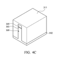
- FIGS. 4A to 4H are perspective views of various stages of forming a semiconductor structure in accordance with some embodiments.
- FIG. 5 is a cross-sectional representation of a semiconductor structure in accordance with some embodiments.
- first and second features are formed in direct contact
- additional features may be formed between the first and second features, such that the first and second features may not be in direct contact
- present disclosure may repeat reference numerals and/or letters in the various examples. This repetition is for the purpose of simplicity and clarity and does not in itself dictate a relationship between the various embodiments and/or configurations discussed.
- spatially relative terms such as “beneath,” “below,” “lower,” “above,” “upper” and the like, may be used herein for ease of description to describe one element or feature's relationship to another element(s) or feature(s) as illustrated in the figures.
- the spatially relative terms are intended to encompass different orientations of the device in use or operation in addition to the orientation depicted in the figures.
- the apparatus may be otherwise oriented (rotated 90 degrees or at other orientations) and the spatially relative descriptors used herein may likewise be interpreted accordingly.
- the semiconductor structure includes an insertion layer formed between an interfacial layer and a gate dielectric layer.
- the insertion layer is made of metal oxide, and the oxygen in the insertion layer can complement the oxygen vacancy in the gate dielectric layer.
- FIGS. 1A to 1D are cross-sectional representations of various stages of forming a semiconductor structure 100 a in accordance with some embodiments.
- a substrate 102 is received in accordance with some embodiments.
- Substrate 102 may be a semiconductor wafer such as a silicon wafer.
- substrate 102 may include elementary semiconductor materials, compound semiconductor materials, and/or alloy semiconductor materials. Examples of the elementary semiconductor materials may be, but are not limited to, crystal silicon, polycrystalline silicon, amorphous silicon, germanium, and/or diamond.
- Examples of the compound semiconductor materials may be, but are not limited to, silicon carbide, gallium arsenic, gallium phosphide, indium phosphide, indium arsenide, and/or indium antimonide.
- Examples of the alloy semiconductor materials may be, but are not limited to, SiGe, GaAsP, AlInAs, AlGaAs, GaInAs, GaInP, and/or GaInAsP.
- a dummy gate structure 104 is formed over substrate 102 , as shown in FIG. 1A in accordance with some embodiments.
- Dummy gate structure 104 includes an interfacial layer 106 , an insertion layer 108 , a gate dielectric layer 110 , and a dummy gate electrode layer 112 in accordance with some embodiments.
- interfacial layer 106 is made of SiO 2 , GeO 2 , HfSiO, SiON, or the like. In some embodiments, interfacial layer 106 has a thickness in a range from about 2 ⁇ to about 50 ⁇ . Interfacial layer 106 may be formed by performing an atomic layer deposition (ALD) process, thermal oxidation process, UV-Ozone oxidation process, or chemical vapor deposition (CVD) process.
- ALD atomic layer deposition
- CVD chemical vapor deposition
- Insertion layer 108 is formed over interfacial layer 106 , and gate dielectric layer 110 is formed over insertion layer 108 , as shown in FIG. 1A in accordance with some embodiments. Insertion layer 108 may be formed to complement the oxygen vacancy in gate dielectric layer 110 . Accordingly, the material used to form insertion layer 108 may contain more oxygen than that used to form gate dielectric layer 110 does. In some embodiments, insertion layer 108 and gate dielectric layer 110 are both made of metal oxide, but the metal oxide which is used to form insertion layer 108 has a higher coordination number than that of the metal oxide which is used to form gate dielectric layer 110 .
- insertion layer 108 is made of M 1 O x .
- M 1 is a metal.
- M 1 is selected from Hf, Al, Y, Ga, Sc, La, Ce, Pr, Nd, Pm, Sm, Eu, Gd, Tb, Dy, Ho, Er, Tm, Yb, or Lu.
- O is oxygen.
- x is a value greater than 4.
- x is in a range from about 5 to about 10.
- insertion layer 108 may be formed to complement the oxygen vacancy in gate dielectric layer 110 , and therefore x should be high enough so that insertion layer 108 can provide enough oxygen to repair the oxygen vacancy in gate dielectric layer 110 .
- x should not be too high, or the dielectric constant of insertion layer 108 may become too high and the performance of the gate structure formed over it in subsequent manufacturing processes may be affected.
- gate dielectric layer 110 is made of M 2 O y .
- M 2 is a metal.
- M 2 is selected from Hf, Al, Y, Ga, Sc, La, Ce, Pr, Nd, Pm, Sm, Eu, Gd, Tb, Dy, Ho, Er, Tm, Yb, or Lu.
- O is oxygen.
- y is less than 5.
- y is in a range from about 1 to 4.
- M 1 and M 2 are the same metals, but the coordination numbers of the materials used to form insertion layer 108 and gate dielectric layer 110 are different.
- insertion layer 108 is made of M 1 O x
- gate dielectric layer 110 is made of M 1 O y
- x is greater than y.
- insertion layer 108 is made of HfO x
- gate dielectric layer 110 is made of HfO y
- x is equal to, or greater than, 5 and y is equal to, or less than, 4.
- the dielectric constant of gate dielectric layer 110 is greater than the dielectric constant of insertion layer 108 . In some embodiments, the dielectric constant of gate dielectric layer 110 is in a range from 18 to 25. In some embodiments, the dielectric constant of insertion layer 108 is in a range from 13 to 17. In some embodiments, the dielectric constant of insertion layer 108 is greater than the dielectric constant of interfacial layer.
- M 1 m O n M 1 is a metal, O is oxygen, m is a value in a range from about 1 to about 2, and n is a value in a range from about 1 to about 3.
- M 1 is Hf, Al, Y, Ga, Sc, La, Ce, Pr, Nd, Pm, Sm, Eu, Gd, Tb, Dy, Ho, Er, Tm, Yb, or Lu.
- a ratio of n to m is in a range from about 5 to about 10.
- Insertion layer 108 has a thickness in a range from about 1 ⁇ to about 15 ⁇ . Insertion layer 108 should be thick enough so that it can provide efficient oxygen to repair the oxygen vacancy of gate dielectric layer 110 . However, insertion layer 108 should not be too thick, or the capacitance of the semiconductor structure may be too high and the performance of the semiconductor structure may be undermined accordingly. Insertion layer 108 may be formed by annealing, chemical vapor deposition (CVD), physical vapor deposition, (PVD), atomic layer deposition (ALD), spin-on coating, or other applicable processes. Gas, such as N 2 , H 2 , O 2 , N 2 O, and/or H 2 O, may be used during the process for forming insertion layer 108 .
- CVD chemical vapor deposition
- PVD physical vapor deposition
- ALD atomic layer deposition
- gate dielectric layer 110 is made of a high-k dielectric material.
- the high-k dielectric material include, but are not limited to, hafnium oxide (HfO 2 ), hafnium silicon oxide (HfSiO), hafnium tantalum oxide (HfTaO), hafnium titanium oxide (HfTiO), hafnium zirconium oxide (HfZrO), zirconium oxide, titanium oxide, aluminum oxide, hafnium dioxide-alumina (HfO 2 —Al 2 O 3 ) alloy, or other applicable dielectric materials.
- Gate dielectric layer 110 may be formed by chemical vapor deposition (CVD), physical vapor deposition, (PVD), atomic layer deposition (ALD), spin-on coating, or other applicable processes. In some embodiments, gate dielectric layer 110 has a thickness in a range from about 10 ⁇ to about 50 ⁇ .
- CVD chemical vapor deposition
- PVD physical vapor deposition
- ALD atomic layer deposition
- spin-on coating or other applicable processes.
- gate dielectric layer 110 has a thickness in a range from about 10 ⁇ to about 50 ⁇ .
- Dummy gate electrode layer 112 is formed over gate dielectric layer 110 , as shown in FIG. 1A in accordance with some embodiments.
- dummy gate electrode layer 112 is made of polysilicon.
- Dummy gate structure 104 may be formed by depositing interfacial layer 106 , insertion layer 108 , gate dielectric layer 110 , and dummy gate electrode layer 112 sequentially and patterning these material layers to form dummy gate structure 104 .
- sealing layers 114 are formed on the sidewalls of dummy gate structure 104 , as shown in FIG. 1B in accordance with some embodiments. Sealing layer 114 may protect dummy gate structure 104 from damage or loss during subsequent processing and may also prevent oxidation during subsequent processing. In some embodiments, sealing layer 114 is made of silicon nitride, silicon oxide, silicon oxynitride, silicon carbide, or other applicable dielectric materials. Sealing layer 114 may include a single layer or multiple layers.
- Spacers 116 are further formed on sealing layer 112 in accordance with some embodiments.
- spacers 116 are made of silicon nitride, silicon oxide, silicon carbide, silicon oxynitride, or other applicable materials.
- Source/drain structures 118 are formed in substrate 102 and is positioned adjacent to dummy gate structure 104 , as shown in FIG. 1B in accordance with some embodiments.
- source/drain structures 118 are formed by using an implantation process or an epitaxial (epi) process.
- source/drain structures 118 include Ge, SiGe, InAs, InGaAs, InSb, GaAs, GaSb, InAlP, InP, or the like.
- a contact etch stop layer (CESL) 120 is formed over substrate 102 , and an interlayer dielectric layer 122 is formed over contact etch stop layer 120 , as shown in FIG. 1B in accordance with some embodiments.
- contact etch stop layer 120 is formed on the sidewalls of spacers 116 and the top surface of source/drain structures 118 in accordance with some embodiments.
- contact etch stop layer 120 is made of silicon nitride, silicon oxynitride, and/or other applicable materials.
- Contact etch stop layer 120 may be formed by chemical vapor deposition (CVD), physical vapor deposition, (PVD), atomic layer deposition (ALD), spin-on coating, or other applicable processes.
- interlayer dielectric layer 122 is made of silicon oxide, silicon nitride, phosphosilicate glass (PSG), borophosphosilicate glass (BPSG), and/or other applicable dielectric materials. Interlayer dielectric layer 122 may be formed by chemical vapor deposition (CVD), physical vapor deposition, (PVD), atomic layer deposition (ALD), spin-on coating, or other applicable processes.
- CVD chemical vapor deposition
- PVD physical vapor deposition
- ALD atomic layer deposition
- spin-on coating or other applicable processes.
- dummy gate electrode layer 112 is removed to form a trench 124 between spacers 116 , as shown in FIG. 1C in accordance with some embodiments.
- a gate structure 126 is formed in trench 124 , as shown in FIG. 1D in accordance with some embodiments.
- gate structure 126 includes a work functional metal layer 128 and a metal gate electrode layer 130 .
- Work function metal layer 128 is tuned to have a proper work function.
- work function metal layer 128 is made of metal nitride. For example, if a P-type work function metal (P-metal) for a PMOS device is desired, TiN, WN, or W may be used. On the other hand, if an N-type work function metal (N-metal) for NMOS devices is desired, TiAl, TiAlN, or TaCN, may be used.
- metal gate electrode layer 130 is made of a conductive material, such as a metal.
- a conductive material such as a metal.
- the conductive materials used to form metal gate electrode 130 may include, but are not limited to, aluminum, copper, tungsten, titanium, tantalum, or other applicable materials.
- the metal of metal gate electrode layer 130 may diffuse toward the layers formed below.
- semiconductor structure 100 a includes insertion layer 108 positioned between interfacial layer 106 and gate dielectric layer 110 .
- the oxygen in insertion layer 108 can complement the oxygen vacancy in gate dielectric layer 110 , so that the threshold voltage of gate structure 126 will not be affected by the oxygen vacancy in gate dielectric layer 110 . Accordingly, the resulting semiconductor structure can have a better uniformity, and the yield of manufacturing semiconductor structures 100 a can be improved.
- FIGS. 2A to 2B are cross-sectional representations of various stages of forming a semiconductor structure 100 b in accordance with some embodiments. Some processes and materials used to form semiconductor structure 100 b may be similar to, or the same as, those used to form semiconductor structure 100 a described previously and are not repeated herein.
- the method for forming semiconductor structure 100 b is similar to that of forming semiconductor structure 100 a , except its interfacial layer, insertion layer, and gate dielectric layer are formed after the dummy gate structure is removed. Similar to those shown in FIGS. 1A to 1C , a dummy gate structure is formed over substrate 102 , and sealing layer 114 and spacers 116 are formed on the sidewalls of the dummy gate structure. In addition, source/drain structure 118 is formed in substrate 102 , and contact etch stop layer 120 and interlayer dielectric layer 122 are formed over substrate 102 . Afterwards, the dummy gate structure is removed to form a trench 224 , as shown in FIG. 2A in accordance with some embodiments.
- interfacial layer 206 is formed on the bottom surface of trench 224 . Processes and materials used to form interfacial layer 206 may be similar to, or the same as, those used to form interfacial layer 106 described previously and are not repeated herein.
- an insertion layer 208 is formed on the top surface of interfacial layer 206 and on the sidewalls of trench 224 , as shown in FIG. 2B in accordance with some embodiments. Processes and materials used to form insertion layer 208 may be similar to, or the same as, those used to form insertion layer 108 described previously and are not repeated herein. In some embodiments, insertion layer 208 is formed by performing a CVD process.
- a gate dielectric layer 210 is formed over insertion layer 208 , as shown in FIG. 2B in accordance with some embodiments. Processes and materials used to form gate dielectric layer 210 may be similar to, or the same as, those used to form gate dielectric layer 110 described previously and are not repeated herein.
- gate structure 226 is formed over gate dielectric layer 210 , as shown in FIG. 2B in accordance with some embodiments. Similar to gate structure 126 , gate structure 226 includes a work function metal layer 228 and a metal gate electrode layer 230 formed over work function metal layer 228 in accordance with some embodiments. Processes and materials used to form work function metal layer 228 and metal gate electrode layer 230 may respectively be similar to, or the same as, those used to form work function metal layer 128 and metal gate electrode layer 130 described previously and are not repeated herein.
- semiconductor structure 100 b includes insertion layer 208 positioned between interfacial layer 206 and gate dielectric layer 210 .
- insertion layer 208 is formed to contain more oxygen than gate dielectric layer does, and therefore insertion layer 208 may be seen as an oxygen source for repairing the oxygen vacancy in gate dielectric layer 110 . Accordingly, the performance of the resulting semiconductor structures 100 b can be improved and better controlled.
- the oxygen vacancy in gate dielectric layer 210 can be repaired by the oxygen in insertion layer 208 , and the uniformity of forming semiconductor structure 100 b can be improved.
- FIG. 3 is a cross-sectional representation of a semiconductor structure 100 c in accordance with some embodiments.
- Semiconductor structure 100 c is similar to, or the same as, semiconductor structure 100 b , except the insertion layer is not formed on the sidewall of sealing layer 114 .
- an insertion layer 208 ′ is formed over interfacial layer 206 .
- the material used to form insertion layer 208 ′ may be similar to, or the same as, that used to form insertion layers 108 and 208 described previously and is not repeated herein.
- the difference between insertion layer 208 ′ and insertion layer 208 is that insertion layer 208 ′ is only formed on the top surface of interfacial layer 206 (i.e. on the bottom surface of the trench formed by removing the dummy gate structure) but not on the sidewalls of sealing layer 114 (i.e. on the sidewalls of the trench formed by removing the dummy gate structure).
- insertion layer 208 ′ is formed by performing a thermal process.
- FIGS. 4A to 4H are perspective views of various stages of forming a semiconductor structure 100 d in accordance with some embodiments.
- a dielectric layer 303 and a mask layer 305 are formed over substrate 102 , and a photo-sensitive layer 307 is formed over mask layer 305 , as shown in FIG. 4A in accordance with some embodiments.
- Dielectric layer 303 may be used as an adhesion layer between substrate 102 and mask layer 305 .
- dielectric layer 303 may also be used as an etch stop layer for etching mask layer 305 .
- dielectric layer 303 is made of silicon oxide.
- Dielectric layer 305 may be formed by using a thermal oxidation process, although other deposition processes may be used in some other embodiments.
- Mask layer 305 may be used as a hard mask during subsequent photolithography processes.
- mask layer 305 is made of silicon nitride.
- Mask layer 305 may be formed by using low-pressure chemical vapor deposition (LPCVD) or plasma enhanced chemical vapor deposition (PECVD), although other deposition processes may also be used in some other embodiments.
- LPCVD low-pressure chemical vapor deposition
- PECVD plasma enhanced chemical vapor deposition
- a fin structure 309 is formed by sequentially etching mask layer 305 , dielectric layer 303 , and substrate 302 through photo-sensitive layer 307 , as shown in FIG. 4B in accordance with some embodiments. Afterwards, photo-sensitive layer 307 is removed. After fin structure 309 is formed, an insulating layer 311 is formed over substrate 102 , as shown in FIG. 4C in accordance with some embodiments. As shown in FIG. 4C , fin structure 309 may be covered by insulating layer 311 .
- insulating layer 311 is made of silicon oxide, silicon nitride, silicon oxynitride, fluoride-doped silicate glass (FSG), or other low-K dielectric materials. Insulating layer 311 may be formed by using a high-density-plasma (HDP) CVD process, although other deposition processes may be used in other embodiments.
- HDP high-density-plasma
- insulating layer 311 is recessed to form an isolation structure 313 , such as a shallow trench isolation structure, around fin structure 309 , as shown in FIG. 4D in accordance with some embodiments.
- Insulating layer 311 may be recessed by a wet etching process or a dry etching process.
- mask layer 306 and dielectric layer 304 are removed.
- a dummy gate structure 304 is formed across fin structure 309 and extends over isolation structure 313 .
- dummy gate structure 304 includes a dummy gate dielectric layer 306 and a dummy gate electrode layer 312 formed over dummy gate dielectric layer 306 .
- dummy gate dielectric layer 306 is made of silicon oxide.
- dummy gate dielectric layer 306 is made of high-k dielectric materials, such as metal oxides, metal nitrides, metal silicates, transition metal-oxides, transition metal-nitrides, transition metal-silicates, or oxynitrides of metals.
- high-k dielectric material examples include, but are not limited to, hafnium oxide (HfO 2 ), hafnium silicon oxide (HfSiO), hafnium silicon oxynitride (HfSiON), hafnium tantalum oxide (HfTaO), hafnium titanium oxide (HfTiO), hafnium zirconium oxide (HfZrO), zirconium oxide, titanium oxide, aluminum oxide, hafnium dioxide-alumina (HfO 2 —Al 2 O 3 ) alloy, or other applicable dielectric materials.
- dummy gate electrode layer 312 is made of polysilicon.
- sealing layers 314 and spacers 316 are formed on the sidewalls of dummy gate structure 304 , as shown in FIG. 4E in accordance with some embodiments. Processes and materials used to form sealing layer 314 and spacers 316 may be similar to, or the same as, those used to form sealing layer 114 and spacers 116 described previously and are not repeated herein.
- source/drain structures 323 are formed in fin structure 309 , as shown in FIG. 4E in accordance with some embodiments.
- portions of fin structure 309 adjacent to dummy gate structure 304 are recessed to form recesses at two sides of fin structure 309 , and a strained material is grown in the recesses by an epitaxial (epi) process.
- the lattice constant of the strained material may be different from the lattice constant of substrate 102 .
- source/drain structures 323 include Ge, SiGe, InAs, InGaAs, InSb, GaAs, GaSb, InAlP, InP, or the like.
- a contact etch stop layer (CESL) 320 is formed over substrate 102 , and an interlayer dielectric (ILD) layer 322 is formed over contact etch stop layer 320 , as shown in FIG. 4F in accordance with some embodiments.
- Processes and materials used to form contact etch stop layer 320 and interlayer dielectric layer 322 may be similar to, or the same as, those used to form contact etch stop layer 120 and interlayer dielectric layer 122 described previously and are not repeated herein.
- a polishing process is performed on interlayer dielectric layer 322 and contact etch stop layer 320 to expose the top surface of dummy gate structure 304 in accordance with some embodiments.
- a chemical mechanical polishing (CMP) process is performed until the top surface of dummy gate structure 304 is exposed.
- dummy gate structure 304 is removed, such that a trench 324 is formed, as shown in FIG. 4G in accordance with some embodiments.
- dummy gate structure 304 is removed by performing a dry etching process.
- dummy gate structure 304 is removed by performing a dry etching process and a wet etching process.
- interfacial layer 306 ′ is formed on the bottom surface of trench 324 , as shown in FIG. 4H in accordance with some embodiments. Processes and materials used to form interfacial layer 306 ′ may be similar to, or the same as, those used to form interfacial layers 106 and 206 described previously and are not repeated herein.
- an insertion layer 308 is formed on the top surface of interfacial layer 306 ′ and on the sidewalls of trench 324 , as shown in FIG. 4H in accordance with some embodiments.
- Processes and materials used to form insertion layer 308 may be similar to, or the same as, those used to form insertion layers 108 , 208 , and 208 ′ described previously and are not repeated herein.
- insertion layer 308 is formed by performing a CVD process.
- a gate dielectric layer 310 is formed over insertion layer 308 , as shown in FIG. 4H in accordance with some embodiments. Processes and materials used to form gate dielectric layer 310 may be similar to, or the same as, those used to form gate dielectric layers 110 and 210 described previously and are not repeated herein.
- gate structure 326 is formed over gate dielectric layer 310 , as shown in FIG. 4H in accordance with some embodiments. Similar to gate structure 126 , gate structure 326 includes a work function metal layer 328 and a metal gate electrode layer 330 formed over work function metal layer 328 in accordance with some embodiments. Processes and materials used to form work function metal layer 328 and metal gate electrode layer 330 may respectively be similar to, or the same as, those used to form work function metal layers 128 and 228 and metal gate electrode layers 130 and 230 described previously and are not repeated herein.
- semiconductor structure 100 d includes insertion layer 308 positioned between interfacial layer 306 ′ and gate dielectric layer 310 .
- the oxygen vacancy in gate dielectric layer 310 can be repaired by the oxygen in insertion layer 308 , and the yield of forming semiconductor structure 100 d can be improved.
- FIG. 5 is a cross-sectional representation of a semiconductor structure 100 e in accordance with some embodiments.
- Semiconductor structure 100 e is similar to, or the same as, semiconductor structures 100 d , except the insertion layer is not formed on the sidewall of sealing layer 114 (similar to semiconductor structure 100 c ).
- an insertion layer 308 ′ is formed over interfacial layer 306 ′.
- the material used to form insertion layer 308 ′ may be similar to, or the same as, that used to form insertion layers 108 , 208 , 208 ′, and 308 described previously and is not repeated herein.
- the difference between insertion layer 308 ′ and insertion layer 308 is that insertion layer 308 ′ is only formed on the top surface of interfacial layer 306 ′ (i.e. on the bottom surface of trench 324 ) but not on the sidewalls of sealing layer 314 (i.e. on the sidewalls of trench 324 ).
- insertion layer 308 ′ is formed by performing a thermal process.
- a gate structure in a semiconductor structure includes a gate dielectric layer and a gate electrode layer formed over the gate dielectric layer.
- the gate dielectric layer is made of a high-k dielectric material, such as a metal oxide
- oxygen vacancy may be formed in the gate dielectric layer during the processes for manufacturing the gate structure.
- the oxygen vacancy may draw negative electrons on the top surface of the substrate and induce an internal electric field. That is, the work function value of the gate structure may be affected by the internal electric field and the uniformity of the resulting semiconductor structure may be poor.
- an insertion layer (e.g. insertion layers 108 , 208 , 208 ′, 308 , and 308 ′) is positioned between an interfacial layer (e.g. interfacial layers 106 , 206 , and 306 ′) and a gate dielectric layer (e.g. gate dielectric layers 110 , 210 , and 310 ).
- the insertion layer is made of a relatively oxygen-rich material, compared to the gate dielectric layer and therefore can be used to complement the oxygen vacancy in the gate dielectric layer.
- the threshold voltage and the work function value of the gate structure will not be affected by the oxygen vacancy in the gate dielectric layer, and the performance of the resulting semiconductor structure (e.g. semiconductor structures 100 a to 100 e ) can be better controlled.
- uniformity and reliability of the semiconductor structure can also be improved, and the yield of the manufacturing processes can be increased.
- the insertion layer is made of a metal oxide such as M 1 O x described previously and can be easily form by any known or future developed processes. That is, no complicated manufacturing process is required, and the cost of the manufacturing process may be relatively low.
- Embodiments of a semiconductor structure and methods for manufacturing the same are provided.
- the semiconductor structure includes an interfacial layer, an insertion layer, and a gate dielectric layer formed over a substrate.
- a gate structure is formed over the gate dielectric layer.
- the insertion layer is positioned between the interfacial layer and the gate dielectric layer.
- the insertion layer is made of a metal oxide which contains a relatively high oxygen therein, compared to the material used to form the gate dielectric layer. Therefore, the insertion layer may be used to complement the oxygen vacancy in the gate dielectric layer, and the threshold voltage of the gate structure formed over the gate dielectric layer may be better controlled. Accordingly, the semiconductor structure may have an improved uniformity, and the yield of the process for manufacturing the semiconductor structure may increase.
- a semiconductor structure in some embodiments, includes a substrate, an interfacial layer formed over the substrate, and an insertion layer formed over the interfacial layer.
- the semiconductor structure further includes a gate dielectric layer formed over the insertion layer and a gate structure formed over the gate dielectric layer.
- the insertion layer is made of M 1 O x , and M 1 is a metal, O is oxygen, and x is a value greater than 4.
- a semiconductor structure in some embodiments, includes a substrate and an interfacial layer formed over the substrate.
- the semiconductor structure further includes an insertion layer formed over the interfacial layer and a gate dielectric layer formed over the insertion layer.
- the semiconductor structure further includes a gate structure formed over the gate dielectric layer.
- the insertion layer is made of a M 1 O x
- the gate dielectric layer is made of M 2 O y , and wherein M 1 is a metal, M 2 is a metal, O is oxygen, and x is a number greater than y.
- a method for manufacturing a semiconductor structure includes forming an interfacial layer over a substrate.
- the method for manufacturing a semiconductor structure further includes forming an insertion layer over the interfacial layer and forming a gate dielectric layer over the insertion layer.
- the method for manufacturing a semiconductor structure further includes forming a gate structure over the gate dielectric layer.
- the insertion layer is made of M 1 m O n , M 1 is a metal, O is oxygen, m is a value in a range from about 1 to about 2, and n is a value in a range from about 1.2 to about 3.5.
Abstract
A semiconductor structure and a method for forming the same are provided. The semiconductor structure includes a substrate, an interfacial layer formed over the substrate, and an insertion layer formed over the interfacial layer. The semiconductor structure further includes a gate dielectric layer formed over the insertion layer and a gate structure formed over the gate dielectric layer. In addition, the insertion layer is made of M1Ox, and M1 is a metal, O is oxygen, and x is a value greater than 4.
Description
Semiconductor devices are used in a variety of electronic applications, such as personal computers, cell phones, digital cameras, and other electronic equipment. Semiconductor devices are typically fabricated by sequentially depositing insulating or dielectric layers, conductive layers, and semiconductor layers of material over a semiconductor substrate, and patterning the various material layers using lithography to form circuit components and elements thereon.
However, although existing semiconductor manufacturing processes have generally been adequate for their intended purposes, as device scaling-down continues, they have not been entirely satisfactory in all respects.
Aspects of the present disclosure are best understood from the following detailed description when read with the accompanying figures. It should be noted that, in accordance with the standard practice in the industry, various features are not drawn to scale. In fact, the dimensions of the various features may be arbitrarily increased or reduced for clarity of discussion.
The following disclosure provides many different embodiments, or examples, for implementing different features of the invention. Specific examples of components and arrangements are described below to simplify the present disclosure. These are, of course, merely examples and are not intended to be limiting. For example, the formation of a first feature over or on a second feature in the description that follows may include embodiments in which the first and second features are formed in direct contact, and may also include embodiments in which additional features may be formed between the first and second features, such that the first and second features may not be in direct contact. In addition, the present disclosure may repeat reference numerals and/or letters in the various examples. This repetition is for the purpose of simplicity and clarity and does not in itself dictate a relationship between the various embodiments and/or configurations discussed.
Furthermore, spatially relative terms, such as “beneath,” “below,” “lower,” “above,” “upper” and the like, may be used herein for ease of description to describe one element or feature's relationship to another element(s) or feature(s) as illustrated in the figures. The spatially relative terms are intended to encompass different orientations of the device in use or operation in addition to the orientation depicted in the figures. The apparatus may be otherwise oriented (rotated 90 degrees or at other orientations) and the spatially relative descriptors used herein may likewise be interpreted accordingly.
Embodiments of semiconductor structures and methods for manufacturing the same are provided. The semiconductor structure includes an insertion layer formed between an interfacial layer and a gate dielectric layer. The insertion layer is made of metal oxide, and the oxygen in the insertion layer can complement the oxygen vacancy in the gate dielectric layer.
A dummy gate structure 104 is formed over substrate 102, as shown in FIG. 1A in accordance with some embodiments. Dummy gate structure 104 includes an interfacial layer 106, an insertion layer 108, a gate dielectric layer 110, and a dummy gate electrode layer 112 in accordance with some embodiments.
In some embodiments, interfacial layer 106 is made of SiO2, GeO2, HfSiO, SiON, or the like. In some embodiments, interfacial layer 106 has a thickness in a range from about 2 Å to about 50 Å. Interfacial layer 106 may be formed by performing an atomic layer deposition (ALD) process, thermal oxidation process, UV-Ozone oxidation process, or chemical vapor deposition (CVD) process.
In some embodiments, insertion layer 108 is made of M1Ox. M1 is a metal. In some embodiments, M1 is selected from Hf, Al, Y, Ga, Sc, La, Ce, Pr, Nd, Pm, Sm, Eu, Gd, Tb, Dy, Ho, Er, Tm, Yb, or Lu. O is oxygen. In some embodiments, x is a value greater than 4. In some embodiments, x is in a range from about 5 to about 10. As described above, insertion layer 108 may be formed to complement the oxygen vacancy in gate dielectric layer 110, and therefore x should be high enough so that insertion layer 108 can provide enough oxygen to repair the oxygen vacancy in gate dielectric layer 110. However, x should not be too high, or the dielectric constant of insertion layer 108 may become too high and the performance of the gate structure formed over it in subsequent manufacturing processes may be affected.
In some embodiments, gate dielectric layer 110 is made of M2Oy. M2 is a metal. In some embodiments, M2 is selected from Hf, Al, Y, Ga, Sc, La, Ce, Pr, Nd, Pm, Sm, Eu, Gd, Tb, Dy, Ho, Er, Tm, Yb, or Lu. O is oxygen. In some embodiments, y is less than 5. In some embodiments, y is in a range from about 1 to 4. In some embodiments, M1 and M2 are the same metals, but the coordination numbers of the materials used to form insertion layer 108 and gate dielectric layer 110 are different. For example, insertion layer 108 is made of M1Ox, and gate dielectric layer 110 is made of M1Oy. In addition, x is greater than y. In some embodiments, insertion layer 108 is made of HfOx, and gate dielectric layer 110 is made of HfOy, while x is equal to, or greater than, 5 and y is equal to, or less than, 4.
In some embodiments, the dielectric constant of gate dielectric layer 110 is greater than the dielectric constant of insertion layer 108. In some embodiments, the dielectric constant of gate dielectric layer 110 is in a range from 18 to 25. In some embodiments, the dielectric constant of insertion layer 108 is in a range from 13 to 17. In some embodiments, the dielectric constant of insertion layer 108 is greater than the dielectric constant of interfacial layer.
In some embodiments, M1 mOn, M1 is a metal, O is oxygen, m is a value in a range from about 1 to about 2, and n is a value in a range from about 1 to about 3. In some embodiments, M1 is Hf, Al, Y, Ga, Sc, La, Ce, Pr, Nd, Pm, Sm, Eu, Gd, Tb, Dy, Ho, Er, Tm, Yb, or Lu. In some embodiments, a ratio of n to m is in a range from about 5 to about 10.
In some embodiments, insertion layer 108 has a thickness in a range from about 1 Å to about 15 Å. Insertion layer 108 should be thick enough so that it can provide efficient oxygen to repair the oxygen vacancy of gate dielectric layer 110. However, insertion layer 108 should not be too thick, or the capacitance of the semiconductor structure may be too high and the performance of the semiconductor structure may be undermined accordingly. Insertion layer 108 may be formed by annealing, chemical vapor deposition (CVD), physical vapor deposition, (PVD), atomic layer deposition (ALD), spin-on coating, or other applicable processes. Gas, such as N2, H2, O2, N2O, and/or H2O, may be used during the process for forming insertion layer 108.
In some embodiments, gate dielectric layer 110 is made of a high-k dielectric material. Examples of the high-k dielectric material include, but are not limited to, hafnium oxide (HfO2), hafnium silicon oxide (HfSiO), hafnium tantalum oxide (HfTaO), hafnium titanium oxide (HfTiO), hafnium zirconium oxide (HfZrO), zirconium oxide, titanium oxide, aluminum oxide, hafnium dioxide-alumina (HfO2—Al2O3) alloy, or other applicable dielectric materials. Gate dielectric layer 110 may be formed by chemical vapor deposition (CVD), physical vapor deposition, (PVD), atomic layer deposition (ALD), spin-on coating, or other applicable processes. In some embodiments, gate dielectric layer 110 has a thickness in a range from about 10 Å to about 50 Å.
Dummy gate electrode layer 112 is formed over gate dielectric layer 110, as shown in FIG. 1A in accordance with some embodiments. In some embodiments, dummy gate electrode layer 112 is made of polysilicon. Dummy gate structure 104 may be formed by depositing interfacial layer 106, insertion layer 108, gate dielectric layer 110, and dummy gate electrode layer 112 sequentially and patterning these material layers to form dummy gate structure 104.
After dummy gate structure 104 is formed, sealing layers 114 are formed on the sidewalls of dummy gate structure 104, as shown in FIG. 1B in accordance with some embodiments. Sealing layer 114 may protect dummy gate structure 104 from damage or loss during subsequent processing and may also prevent oxidation during subsequent processing. In some embodiments, sealing layer 114 is made of silicon nitride, silicon oxide, silicon oxynitride, silicon carbide, or other applicable dielectric materials. Sealing layer 114 may include a single layer or multiple layers.
After source/drain structures 118 are formed in substrate 102, a contact etch stop layer (CESL) 120 is formed over substrate 102, and an interlayer dielectric layer 122 is formed over contact etch stop layer 120, as shown in FIG. 1B in accordance with some embodiments. As shown in FIG. 1B , contact etch stop layer 120 is formed on the sidewalls of spacers 116 and the top surface of source/drain structures 118 in accordance with some embodiments. In some embodiments, contact etch stop layer 120 is made of silicon nitride, silicon oxynitride, and/or other applicable materials. Contact etch stop layer 120 may be formed by chemical vapor deposition (CVD), physical vapor deposition, (PVD), atomic layer deposition (ALD), spin-on coating, or other applicable processes.
In some embodiments, interlayer dielectric layer 122 is made of silicon oxide, silicon nitride, phosphosilicate glass (PSG), borophosphosilicate glass (BPSG), and/or other applicable dielectric materials. Interlayer dielectric layer 122 may be formed by chemical vapor deposition (CVD), physical vapor deposition, (PVD), atomic layer deposition (ALD), spin-on coating, or other applicable processes.
After interlayer dielectric layer 122 is formed, dummy gate electrode layer 112 is removed to form a trench 124 between spacers 116, as shown in FIG. 1C in accordance with some embodiments. Afterwards, a gate structure 126 is formed in trench 124, as shown in FIG. 1D in accordance with some embodiments.
In some embodiments, gate structure 126 includes a work functional metal layer 128 and a metal gate electrode layer 130. Work function metal layer 128 is tuned to have a proper work function. In some embodiments, work function metal layer 128 is made of metal nitride. For example, if a P-type work function metal (P-metal) for a PMOS device is desired, TiN, WN, or W may be used. On the other hand, if an N-type work function metal (N-metal) for NMOS devices is desired, TiAl, TiAlN, or TaCN, may be used.
In some embodiments, metal gate electrode layer 130 is made of a conductive material, such as a metal. Examples of the conductive materials used to form metal gate electrode 130 may include, but are not limited to, aluminum, copper, tungsten, titanium, tantalum, or other applicable materials. As described previously, in subsequent processes, the metal of metal gate electrode layer 130 may diffuse toward the layers formed below.
As shown in FIG. 1D , semiconductor structure 100 a includes insertion layer 108 positioned between interfacial layer 106 and gate dielectric layer 110. The oxygen in insertion layer 108 can complement the oxygen vacancy in gate dielectric layer 110, so that the threshold voltage of gate structure 126 will not be affected by the oxygen vacancy in gate dielectric layer 110. Accordingly, the resulting semiconductor structure can have a better uniformity, and the yield of manufacturing semiconductor structures 100 a can be improved.
The method for forming semiconductor structure 100 b is similar to that of forming semiconductor structure 100 a, except its interfacial layer, insertion layer, and gate dielectric layer are formed after the dummy gate structure is removed. Similar to those shown in FIGS. 1A to 1C , a dummy gate structure is formed over substrate 102, and sealing layer 114 and spacers 116 are formed on the sidewalls of the dummy gate structure. In addition, source/drain structure 118 is formed in substrate 102, and contact etch stop layer 120 and interlayer dielectric layer 122 are formed over substrate 102. Afterwards, the dummy gate structure is removed to form a trench 224, as shown in FIG. 2A in accordance with some embodiments.
Unlike the structure shown in FIG. 1C , the dummy gate structure is completely removed, and therefore the top surface of substrate 102 is exposed by trench 224. After trench 224 is formed, an interfacial layer 206 is formed on the bottom surface of trench 224. Processes and materials used to form interfacial layer 206 may be similar to, or the same as, those used to form interfacial layer 106 described previously and are not repeated herein.
After interfacial layer 206 is formed, an insertion layer 208 is formed on the top surface of interfacial layer 206 and on the sidewalls of trench 224, as shown in FIG. 2B in accordance with some embodiments. Processes and materials used to form insertion layer 208 may be similar to, or the same as, those used to form insertion layer 108 described previously and are not repeated herein. In some embodiments, insertion layer 208 is formed by performing a CVD process.
After insertion layer 208 is formed, a gate dielectric layer 210 is formed over insertion layer 208, as shown in FIG. 2B in accordance with some embodiments. Processes and materials used to form gate dielectric layer 210 may be similar to, or the same as, those used to form gate dielectric layer 110 described previously and are not repeated herein.
Next, a gate structure 226 is formed over gate dielectric layer 210, as shown in FIG. 2B in accordance with some embodiments. Similar to gate structure 126, gate structure 226 includes a work function metal layer 228 and a metal gate electrode layer 230 formed over work function metal layer 228 in accordance with some embodiments. Processes and materials used to form work function metal layer 228 and metal gate electrode layer 230 may respectively be similar to, or the same as, those used to form work function metal layer 128 and metal gate electrode layer 130 described previously and are not repeated herein.
As shown in FIG. 2B , semiconductor structure 100 b includes insertion layer 208 positioned between interfacial layer 206 and gate dielectric layer 210. As described previously, insertion layer 208 is formed to contain more oxygen than gate dielectric layer does, and therefore insertion layer 208 may be seen as an oxygen source for repairing the oxygen vacancy in gate dielectric layer 110. Accordingly, the performance of the resulting semiconductor structures 100 b can be improved and better controlled.
Therefore, the oxygen vacancy in gate dielectric layer 210 can be repaired by the oxygen in insertion layer 208, and the uniformity of forming semiconductor structure 100 b can be improved.
More specifically, processes similar to those shown in FIG. 2A to 2B may be performed. However, instead of insertion layer 208, an insertion layer 208′ is formed over interfacial layer 206. The material used to form insertion layer 208′ may be similar to, or the same as, that used to form insertion layers 108 and 208 described previously and is not repeated herein. The difference between insertion layer 208′ and insertion layer 208 is that insertion layer 208′ is only formed on the top surface of interfacial layer 206 (i.e. on the bottom surface of the trench formed by removing the dummy gate structure) but not on the sidewalls of sealing layer 114 (i.e. on the sidewalls of the trench formed by removing the dummy gate structure). In some embodiments, insertion layer 208′ is formed by performing a thermal process.
Next, a fin structure 309 is formed by sequentially etching mask layer 305, dielectric layer 303, and substrate 302 through photo-sensitive layer 307, as shown in FIG. 4B in accordance with some embodiments. Afterwards, photo-sensitive layer 307 is removed. After fin structure 309 is formed, an insulating layer 311 is formed over substrate 102, as shown in FIG. 4C in accordance with some embodiments. As shown in FIG. 4C , fin structure 309 may be covered by insulating layer 311. In some embodiments, insulating layer 311 is made of silicon oxide, silicon nitride, silicon oxynitride, fluoride-doped silicate glass (FSG), or other low-K dielectric materials. Insulating layer 311 may be formed by using a high-density-plasma (HDP) CVD process, although other deposition processes may be used in other embodiments.
Next, insulating layer 311 is recessed to form an isolation structure 313, such as a shallow trench isolation structure, around fin structure 309, as shown in FIG. 4D in accordance with some embodiments. Insulating layer 311 may be recessed by a wet etching process or a dry etching process. In addition, mask layer 306 and dielectric layer 304 are removed.
Afterwards, a dummy gate structure 304 is formed across fin structure 309 and extends over isolation structure 313. In some embodiments, dummy gate structure 304 includes a dummy gate dielectric layer 306 and a dummy gate electrode layer 312 formed over dummy gate dielectric layer 306. In some embodiments, dummy gate dielectric layer 306 is made of silicon oxide. In some embodiments, dummy gate dielectric layer 306 is made of high-k dielectric materials, such as metal oxides, metal nitrides, metal silicates, transition metal-oxides, transition metal-nitrides, transition metal-silicates, or oxynitrides of metals. Examples of the high-k dielectric material include, but are not limited to, hafnium oxide (HfO2), hafnium silicon oxide (HfSiO), hafnium silicon oxynitride (HfSiON), hafnium tantalum oxide (HfTaO), hafnium titanium oxide (HfTiO), hafnium zirconium oxide (HfZrO), zirconium oxide, titanium oxide, aluminum oxide, hafnium dioxide-alumina (HfO2—Al2O3) alloy, or other applicable dielectric materials. In some embodiments, dummy gate electrode layer 312 is made of polysilicon.
After dummy gate structure 304 is formed, sealing layers 314 and spacers 316 are formed on the sidewalls of dummy gate structure 304, as shown in FIG. 4E in accordance with some embodiments. Processes and materials used to form sealing layer 314 and spacers 316 may be similar to, or the same as, those used to form sealing layer 114 and spacers 116 described previously and are not repeated herein.
Next, source/drain structures 323 are formed in fin structure 309, as shown in FIG. 4E in accordance with some embodiments. In some embodiments, portions of fin structure 309 adjacent to dummy gate structure 304 are recessed to form recesses at two sides of fin structure 309, and a strained material is grown in the recesses by an epitaxial (epi) process. In addition, the lattice constant of the strained material may be different from the lattice constant of substrate 102. In some embodiments, source/drain structures 323 include Ge, SiGe, InAs, InGaAs, InSb, GaAs, GaSb, InAlP, InP, or the like.
After source/drain structures 323 are formed, a contact etch stop layer (CESL) 320 is formed over substrate 102, and an interlayer dielectric (ILD) layer 322 is formed over contact etch stop layer 320, as shown in FIG. 4F in accordance with some embodiments. Processes and materials used to form contact etch stop layer 320 and interlayer dielectric layer 322 may be similar to, or the same as, those used to form contact etch stop layer 120 and interlayer dielectric layer 122 described previously and are not repeated herein.
Next, a polishing process is performed on interlayer dielectric layer 322 and contact etch stop layer 320 to expose the top surface of dummy gate structure 304 in accordance with some embodiments. In some embodiments, a chemical mechanical polishing (CMP) process is performed until the top surface of dummy gate structure 304 is exposed.
After the polishing process is performed, dummy gate structure 304 is removed, such that a trench 324 is formed, as shown in FIG. 4G in accordance with some embodiments. In some embodiments, dummy gate structure 304 is removed by performing a dry etching process. In some embodiments, dummy gate structure 304 is removed by performing a dry etching process and a wet etching process.
After trench 324 is formed, an interfacial layer 306′ is formed on the bottom surface of trench 324, as shown in FIG. 4H in accordance with some embodiments. Processes and materials used to form interfacial layer 306′ may be similar to, or the same as, those used to form interfacial layers 106 and 206 described previously and are not repeated herein.
After interfacial layer 306′ is formed, an insertion layer 308 is formed on the top surface of interfacial layer 306′ and on the sidewalls of trench 324, as shown in FIG. 4H in accordance with some embodiments. Processes and materials used to form insertion layer 308 may be similar to, or the same as, those used to form insertion layers 108, 208, and 208′ described previously and are not repeated herein. In some embodiments, insertion layer 308 is formed by performing a CVD process.
After insertion layer 308 is formed, a gate dielectric layer 310 is formed over insertion layer 308, as shown in FIG. 4H in accordance with some embodiments. Processes and materials used to form gate dielectric layer 310 may be similar to, or the same as, those used to form gate dielectric layers 110 and 210 described previously and are not repeated herein.
Next, a gate structure 326 is formed over gate dielectric layer 310, as shown in FIG. 4H in accordance with some embodiments. Similar to gate structure 126, gate structure 326 includes a work function metal layer 328 and a metal gate electrode layer 330 formed over work function metal layer 328 in accordance with some embodiments. Processes and materials used to form work function metal layer 328 and metal gate electrode layer 330 may respectively be similar to, or the same as, those used to form work function metal layers 128 and 228 and metal gate electrode layers 130 and 230 described previously and are not repeated herein.
As shown in FIG. 4H , semiconductor structure 100 d includes insertion layer 308 positioned between interfacial layer 306′ and gate dielectric layer 310. As described previously, the oxygen vacancy in gate dielectric layer 310 can be repaired by the oxygen in insertion layer 308, and the yield of forming semiconductor structure 100 d can be improved.
More specifically, processes similar to those shown in FIG. 4A to 4H may be performed. However, instead of insertion layer 308, an insertion layer 308′ is formed over interfacial layer 306′. The material used to form insertion layer 308′ may be similar to, or the same as, that used to form insertion layers 108, 208, 208′, and 308 described previously and is not repeated herein. The difference between insertion layer 308′ and insertion layer 308 is that insertion layer 308′ is only formed on the top surface of interfacial layer 306′ (i.e. on the bottom surface of trench 324) but not on the sidewalls of sealing layer 314 (i.e. on the sidewalls of trench 324). In some embodiments, insertion layer 308′ is formed by performing a thermal process.
Generally, a gate structure in a semiconductor structure includes a gate dielectric layer and a gate electrode layer formed over the gate dielectric layer. However, when the gate dielectric layer is made of a high-k dielectric material, such as a metal oxide, oxygen vacancy may be formed in the gate dielectric layer during the processes for manufacturing the gate structure. The oxygen vacancy may draw negative electrons on the top surface of the substrate and induce an internal electric field. That is, the work function value of the gate structure may be affected by the internal electric field and the uniformity of the resulting semiconductor structure may be poor.
Accordingly, in some embodiments of the disclosure, an insertion layer (e.g. insertion layers 108, 208, 208′, 308, and 308′) is positioned between an interfacial layer (e.g. interfacial layers 106, 206, and 306′) and a gate dielectric layer (e.g. gate dielectric layers 110, 210, and 310). The insertion layer is made of a relatively oxygen-rich material, compared to the gate dielectric layer and therefore can be used to complement the oxygen vacancy in the gate dielectric layer. Accordingly, the threshold voltage and the work function value of the gate structure will not be affected by the oxygen vacancy in the gate dielectric layer, and the performance of the resulting semiconductor structure (e.g. semiconductor structures 100 a to 100 e) can be better controlled. In addition, uniformity and reliability of the semiconductor structure can also be improved, and the yield of the manufacturing processes can be increased.
In some embodiments, the insertion layer is made of a metal oxide such as M1Ox described previously and can be easily form by any known or future developed processes. That is, no complicated manufacturing process is required, and the cost of the manufacturing process may be relatively low.
Embodiments of a semiconductor structure and methods for manufacturing the same are provided. The semiconductor structure includes an interfacial layer, an insertion layer, and a gate dielectric layer formed over a substrate. A gate structure is formed over the gate dielectric layer. The insertion layer is positioned between the interfacial layer and the gate dielectric layer. The insertion layer is made of a metal oxide which contains a relatively high oxygen therein, compared to the material used to form the gate dielectric layer. Therefore, the insertion layer may be used to complement the oxygen vacancy in the gate dielectric layer, and the threshold voltage of the gate structure formed over the gate dielectric layer may be better controlled. Accordingly, the semiconductor structure may have an improved uniformity, and the yield of the process for manufacturing the semiconductor structure may increase.
In some embodiments, a semiconductor structure is provided. The semiconductor structure includes a substrate, an interfacial layer formed over the substrate, and an insertion layer formed over the interfacial layer. The semiconductor structure further includes a gate dielectric layer formed over the insertion layer and a gate structure formed over the gate dielectric layer. In addition, the insertion layer is made of M1Ox, and M1 is a metal, O is oxygen, and x is a value greater than 4.
In some embodiments, a semiconductor structure is provided. The semiconductor structure includes a substrate and an interfacial layer formed over the substrate. The semiconductor structure further includes an insertion layer formed over the interfacial layer and a gate dielectric layer formed over the insertion layer. The semiconductor structure further includes a gate structure formed over the gate dielectric layer. In addition, the insertion layer is made of a M1Ox, the gate dielectric layer is made of M2Oy, and wherein M1 is a metal, M2 is a metal, O is oxygen, and x is a number greater than y.
In some embodiments, a method for manufacturing a semiconductor structure is provided. The method for manufacturing a semiconductor structure includes forming an interfacial layer over a substrate. The method for manufacturing a semiconductor structure further includes forming an insertion layer over the interfacial layer and forming a gate dielectric layer over the insertion layer. The method for manufacturing a semiconductor structure further includes forming a gate structure over the gate dielectric layer. In addition, the insertion layer is made of M1 mOn, M1 is a metal, O is oxygen, m is a value in a range from about 1 to about 2, and n is a value in a range from about 1.2 to about 3.5.
The foregoing outlines features of several embodiments so that those skilled in the art may better understand the aspects of the present disclosure. Those skilled in the art should appreciate that they may readily use the present disclosure as a basis for designing or modifying other processes and structures for carrying out the same purposes and/or achieving the same advantages of the embodiments introduced herein. Those skilled in the art should also realize that such equivalent constructions do not depart from the spirit and scope of the present disclosure, and that they may make various changes, substitutions, and alterations herein without departing from the spirit and scope of the present disclosure.
Claims (20)
1. A semiconductor structure, comprising:
a substrate;
an interfacial layer formed over the substrate;
an insertion layer formed over the interfacial layer;
a gate dielectric layer formed over the insertion layer; and
a gate structure formed over the gate dielectric layer,
wherein the insertion layer is made of M1Ox, and M1 is a metal, O is oxygen, and x is a value greater than 4.
2. The semiconductor structure as claimed in claim 1 , wherein M1 is selected from Hf, Al, Y, Ga, Sc, La, Ce, Pr, Nd, Pm, Sm, Eu, Gd, Tb, Dy, Ho, Er, Tm, Yb, or Lu.
3. The semiconductor structure as claimed in claim 1 , wherein the gate dielectric layer is made of M2Oy, M2 is a metal, and y is in a range from about 1 to 4.
4. The semiconductor structure as claimed in claim 3 , wherein x is in a range from about 5 to about 10.
5. The semiconductor structure as claimed in claim 1 , wherein a dielectric constant of the gate dielectric layer is greater than a dielectric constant of the insertion layer.
6. The semiconductor structure as claimed in claim 1 , wherein the gate dielectric layer is made of M1Oy, and y is in a range from about 1 to 4.
7. The semiconductor structure as claimed in claim 1 , wherein a thickness of the insertion layer is in a range from about 1 Å to about 15 Å.
8. A semiconductor structure, comprising:
a substrate;
an interfacial layer formed over the substrate;
an insertion layer formed over the interfacial layer;
a gate dielectric layer formed over the insertion layer; and
a gate structure formed over the gate dielectric layer,
wherein the insertion layer is made of a M1Ox, the gate dielectric layer is made of M2Oy, and wherein M1 is a metal, M2 is a metal, O is oxygen, and x is a number greater than y.
9. The semiconductor structure as claimed in claim 8 , wherein x is in a range from about 5 to about 10.
10. The semiconductor structure as claimed in claim 8 , wherein y is in a range from about 1 to about 4.
11. The semiconductor structure as claimed in claim 8 , wherein M1 and M2 are individually selected from Hf, Al, Y, Ga, Sc, La, Ce, Pr, Nd, Pm, Sm, Eu, Gd, Tb, Dy, Ho, Er, Tm, Yb, or Lu.
12. The semiconductor structure as claimed in claim 8 , wherein M1 and M2 are the same metal.
13. The semiconductor structure as claimed in claim 8 , wherein a dielectric constant of the gate dielectric layer is greater than a dielectric constant of the insertion layer.
14. A method for manufacturing a semiconductor structure, comprising:
forming an interfacial layer over a substrate;
forming an insertion layer over the interfacial layer;
forming a gate dielectric layer over the insertion layer; and
forming a gate structure over the gate dielectric layer,
wherein the insertion layer is made of M1 mOn, M1 is a metal, O is oxygen, m is a value in a range from about 1 to about 2, and n is a value in a range from about 1.2 to about 3.5.
15. The method for manufacturing a semiconductor structure as claimed in claim 14 , wherein a ratio of n to m is in a range from about 5 to about 10.
16. The method for manufacturing a semiconductor structure as claimed in claim 14 , wherein M1 is selected from Hf, Al, Y, Ga, Sc, La, Ce, Pr, Nd, Pm, Sm, Eu, Gd, Tb, Dy, Ho, Er, Tm, Yb, or Lu.
17. The method for manufacturing a semiconductor structure as claimed in claim 14 , wherein the gate structure comprises:
a work function metal layer formed over the gate dielectric layer; and
a gate electrode layer formed over the work function metal layer.
18. The method for manufacturing a semiconductor structure as claimed in claim 14 , wherein a dielectric constant of the gate dielectric layer is greater than a dielectric constant of the insertion layer.
19. The method for manufacturing a semiconductor structure as claimed in claim 14 , wherein the insertion layer is made of HfOn, and the gate dielectric layer is made of HfOp, and p is in a range of about 1 to about 4.
20. The method for manufacturing a semiconductor structure as claimed in claim 14 , wherein a dielectric constant of the insertion layer is greater than a dielectric constant of the interfacial layer.
Priority Applications (7)
| Application Number | Priority Date | Filing Date | Title |
|---|---|---|---|
| US14/918,054 US9515158B1 (en) | 2015-10-20 | 2015-10-20 | Semiconductor structure with insertion layer and method for manufacturing the same |
| DE102016100008.6A DE102016100008B4 (en) | 2015-10-20 | 2016-01-02 | Semiconductor structure with insertion layer and process for its production |
| KR1020160006503A KR20170046048A (en) | 2015-10-20 | 2016-01-19 | Semiconductor structure with insertion layer and method for manufacturing the same |
| TW105124399A TWI619250B (en) | 2015-10-20 | 2016-08-02 | Semiconductor structures and methods for forming the same |
| CN201610641281.8A CN106601794B (en) | 2015-10-20 | 2016-08-08 | Semiconductor structure and its manufacturing method with insert layer |
| US15/369,460 US9960246B2 (en) | 2015-10-20 | 2016-12-05 | Semiconductor structure with insertion layer and method for manufacturing the same |
| KR1020170144719A KR102311437B1 (en) | 2015-10-20 | 2017-11-01 | Semiconductor structure with insertion layer and method for manufacturing the same |
Applications Claiming Priority (1)
| Application Number | Priority Date | Filing Date | Title |
|---|---|---|---|
| US14/918,054 US9515158B1 (en) | 2015-10-20 | 2015-10-20 | Semiconductor structure with insertion layer and method for manufacturing the same |
Related Child Applications (1)
| Application Number | Title | Priority Date | Filing Date |
|---|---|---|---|
| US15/369,460 Continuation US9960246B2 (en) | 2015-10-20 | 2016-12-05 | Semiconductor structure with insertion layer and method for manufacturing the same |
Publications (1)
| Publication Number | Publication Date |
|---|---|
| US9515158B1 true US9515158B1 (en) | 2016-12-06 |
Family
ID=57399958
Family Applications (2)
| Application Number | Title | Priority Date | Filing Date |
|---|---|---|---|
| US14/918,054 Active US9515158B1 (en) | 2015-10-20 | 2015-10-20 | Semiconductor structure with insertion layer and method for manufacturing the same |
| US15/369,460 Active US9960246B2 (en) | 2015-10-20 | 2016-12-05 | Semiconductor structure with insertion layer and method for manufacturing the same |
Family Applications After (1)
| Application Number | Title | Priority Date | Filing Date |
|---|---|---|---|
| US15/369,460 Active US9960246B2 (en) | 2015-10-20 | 2016-12-05 | Semiconductor structure with insertion layer and method for manufacturing the same |
Country Status (5)
| Country | Link |
|---|---|
| US (2) | US9515158B1 (en) |
| KR (2) | KR20170046048A (en) |
| CN (1) | CN106601794B (en) |
| DE (1) | DE102016100008B4 (en) |
| TW (1) | TWI619250B (en) |
Cited By (2)
| Publication number | Priority date | Publication date | Assignee | Title |
|---|---|---|---|---|
| US20170110555A1 (en) * | 2015-10-20 | 2017-04-20 | Taiwan Semiconductor Manufacturing Co., Ltd. | Semiconductor structure with insertion layer and method for manufacturing the same |
| US20190371611A1 (en) * | 2016-09-12 | 2019-12-05 | International Business Machines Corporation | Formation of pure silicon oxide interfacial layer on silicon-germanium channel field effect transistor device |
Families Citing this family (2)
| Publication number | Priority date | Publication date | Assignee | Title |
|---|---|---|---|---|
| US10522358B2 (en) * | 2017-08-31 | 2019-12-31 | Taiwan Semiconductor Manufacturing Company, Ltd. | FinFET device and methods of forming same |
| US11227932B2 (en) * | 2018-05-16 | 2022-01-18 | Taiwan Semiconductor Manufacturing Company, Ltd. | FinFET devices with a fin top hardmask |
Citations (16)
| Publication number | Priority date | Publication date | Assignee | Title |
|---|---|---|---|---|
| US20020195643A1 (en) * | 2001-06-21 | 2002-12-26 | Matsushita Electric Industrial Co., Ltd. | Semiconductor device and method for producing the same |
| US20030057504A1 (en) * | 2001-09-27 | 2003-03-27 | Kouichi Muraoka | Seminconductor device and method of manufacturing the same |
| US20040214365A1 (en) * | 2002-11-14 | 2004-10-28 | Sharp Laboratories Of America, Inc. | Deposition oxide with improved oxygen bonding |
| US6858444B2 (en) * | 2001-03-15 | 2005-02-22 | Micron Technology, Inc. | Method for making a ferroelectric memory transistor |
| US20060054950A1 (en) * | 2004-09-10 | 2006-03-16 | In-Gyu Baek | Non-volatile memory cells employing a transition metal oxide layer as a data storage material layer and methods of manufacturing the same |
| US20060118858A1 (en) * | 2004-10-08 | 2006-06-08 | Samsung Electronics Co., Ltd. | Non-volatile semiconductor memory device with alternative metal gate material |
| US20100207243A1 (en) * | 2009-02-16 | 2010-08-19 | Weon-Hong Kim | Semiconductor device and method of fabricating the same |
| US7838875B1 (en) * | 2003-01-22 | 2010-11-23 | Tsang Dean Z | Metal transistor device |
| US8143092B2 (en) * | 2008-03-10 | 2012-03-27 | Pragati Kumar | Methods for forming resistive switching memory elements by heating deposited layers |
| US20130062581A1 (en) * | 2009-12-23 | 2013-03-14 | Merck Patent Gmbh | Composition for the preparation of organic electronic (oe) devices |
| US20140319619A1 (en) | 2008-09-15 | 2014-10-30 | Taiwan Semiconductor Manufacturing Company, Ltd. | Method of forming a single metal that performs n and p work functions in high-k/metal gate devices |
| US20140346495A1 (en) * | 2013-05-24 | 2014-11-27 | Chan- Long Shieh | Stable high mobility motft and fabrication at low temperature |
| US20150053966A1 (en) * | 2011-10-07 | 2015-02-26 | Evonik Degussa Gmbh | Method for producing high-performing and electrically stable semi-conductive metal oxide layers, layers produced according to the method and use thereof |
| US20150104933A1 (en) | 2013-10-16 | 2015-04-16 | Taiwan Semiconductor Manufacturing Company Limited | Systems and methods for annealing semiconductor device structures using microwave radiation |
| US20150145073A1 (en) | 2013-11-26 | 2015-05-28 | Taiwan Semiconductor Manufacturing Company Limited | Low-k dielectric sidewall spacer treatment |
| US20150340498A1 (en) * | 2006-12-11 | 2015-11-26 | Sony Corporation | Metal oxide semiconductor having epitaxial source drain regions and a method of manufacturing same using dummy gate process |
Family Cites Families (14)
| Publication number | Priority date | Publication date | Assignee | Title |
|---|---|---|---|---|
| US6436774B1 (en) | 2001-01-26 | 2002-08-20 | Chartered Semiconductor Manufacturing Ltd. | Method for forming variable-K gate dielectric |
| DE10350702B4 (en) | 2003-10-30 | 2007-08-09 | Infineon Technologies Ag | Semiconductor device having a capacitive structure, which is robust against defects of a dielectric layer |
| US20050153571A1 (en) * | 2003-11-17 | 2005-07-14 | Yoshihide Senzaki | Nitridation of high-k dielectric films |
| CN101211970B (en) * | 2006-12-28 | 2012-01-25 | 中芯国际集成电路制造(上海)有限公司 | Semiconductor device and producing method thereof |
| KR101377069B1 (en) * | 2008-05-23 | 2014-03-24 | 삼성전자주식회사 | Semiconductor device and method of forming thereof |
| US7776757B2 (en) * | 2009-01-15 | 2010-08-17 | Taiwan Semiconductor Manufacturing Company, Ltd. | Method of fabricating high-k metal gate devices |
| JP2010206099A (en) | 2009-03-05 | 2010-09-16 | Fujitsu Semiconductor Ltd | Semiconductor element and method of manufacturing the same |
| US8569135B2 (en) | 2011-07-20 | 2013-10-29 | International Business Machines Corporation | Replacement gate electrode with planar work function material layers |
| US20130075831A1 (en) * | 2011-09-24 | 2013-03-28 | Taiwan Semiconductor Manufacturing Company, Ltd. | Metal gate stack having tialn blocking/wetting layer |
| DE112011105973T5 (en) | 2011-12-19 | 2014-09-25 | Intel Corporation | Semiconductor device with metallic source and drain regions |
| KR102238682B1 (en) | 2013-02-28 | 2021-04-08 | 가부시키가이샤 한도오따이 에네루기 켄큐쇼 | Semiconductor device and method for manufacturing the same |
| ES2699328T3 (en) | 2013-10-18 | 2019-02-08 | Woehner Gmbh & Co Kg Elektrotechnische Systeme | Contact protection system for power bars |
| CN105321820B (en) | 2014-07-08 | 2018-09-14 | 台湾积体电路制造股份有限公司 | Layout designs are changed to reduce turning sphering effect by OPC |
| US9515158B1 (en) * | 2015-10-20 | 2016-12-06 | Taiwan Semiconductor Manufacturing Co., Ltd. | Semiconductor structure with insertion layer and method for manufacturing the same |
-
2015
- 2015-10-20 US US14/918,054 patent/US9515158B1/en active Active
-
2016
- 2016-01-02 DE DE102016100008.6A patent/DE102016100008B4/en active Active
- 2016-01-19 KR KR1020160006503A patent/KR20170046048A/en active Application Filing
- 2016-08-02 TW TW105124399A patent/TWI619250B/en active
- 2016-08-08 CN CN201610641281.8A patent/CN106601794B/en active Active
- 2016-12-05 US US15/369,460 patent/US9960246B2/en active Active
-
2017
- 2017-11-01 KR KR1020170144719A patent/KR102311437B1/en active IP Right Grant
Patent Citations (16)
| Publication number | Priority date | Publication date | Assignee | Title |
|---|---|---|---|---|
| US6858444B2 (en) * | 2001-03-15 | 2005-02-22 | Micron Technology, Inc. | Method for making a ferroelectric memory transistor |
| US20020195643A1 (en) * | 2001-06-21 | 2002-12-26 | Matsushita Electric Industrial Co., Ltd. | Semiconductor device and method for producing the same |
| US20030057504A1 (en) * | 2001-09-27 | 2003-03-27 | Kouichi Muraoka | Seminconductor device and method of manufacturing the same |
| US20040214365A1 (en) * | 2002-11-14 | 2004-10-28 | Sharp Laboratories Of America, Inc. | Deposition oxide with improved oxygen bonding |
| US7838875B1 (en) * | 2003-01-22 | 2010-11-23 | Tsang Dean Z | Metal transistor device |
| US20060054950A1 (en) * | 2004-09-10 | 2006-03-16 | In-Gyu Baek | Non-volatile memory cells employing a transition metal oxide layer as a data storage material layer and methods of manufacturing the same |
| US20060118858A1 (en) * | 2004-10-08 | 2006-06-08 | Samsung Electronics Co., Ltd. | Non-volatile semiconductor memory device with alternative metal gate material |
| US20150340498A1 (en) * | 2006-12-11 | 2015-11-26 | Sony Corporation | Metal oxide semiconductor having epitaxial source drain regions and a method of manufacturing same using dummy gate process |
| US8143092B2 (en) * | 2008-03-10 | 2012-03-27 | Pragati Kumar | Methods for forming resistive switching memory elements by heating deposited layers |
| US20140319619A1 (en) | 2008-09-15 | 2014-10-30 | Taiwan Semiconductor Manufacturing Company, Ltd. | Method of forming a single metal that performs n and p work functions in high-k/metal gate devices |
| US20100207243A1 (en) * | 2009-02-16 | 2010-08-19 | Weon-Hong Kim | Semiconductor device and method of fabricating the same |
| US20130062581A1 (en) * | 2009-12-23 | 2013-03-14 | Merck Patent Gmbh | Composition for the preparation of organic electronic (oe) devices |
| US20150053966A1 (en) * | 2011-10-07 | 2015-02-26 | Evonik Degussa Gmbh | Method for producing high-performing and electrically stable semi-conductive metal oxide layers, layers produced according to the method and use thereof |
| US20140346495A1 (en) * | 2013-05-24 | 2014-11-27 | Chan- Long Shieh | Stable high mobility motft and fabrication at low temperature |
| US20150104933A1 (en) | 2013-10-16 | 2015-04-16 | Taiwan Semiconductor Manufacturing Company Limited | Systems and methods for annealing semiconductor device structures using microwave radiation |
| US20150145073A1 (en) | 2013-11-26 | 2015-05-28 | Taiwan Semiconductor Manufacturing Company Limited | Low-k dielectric sidewall spacer treatment |
Cited By (5)
| Publication number | Priority date | Publication date | Assignee | Title |
|---|---|---|---|---|
| US20170110555A1 (en) * | 2015-10-20 | 2017-04-20 | Taiwan Semiconductor Manufacturing Co., Ltd. | Semiconductor structure with insertion layer and method for manufacturing the same |
| US9960246B2 (en) * | 2015-10-20 | 2018-05-01 | Taiwan Semiconductor Manufacturing Co., Ltd. | Semiconductor structure with insertion layer and method for manufacturing the same |
| US20190371611A1 (en) * | 2016-09-12 | 2019-12-05 | International Business Machines Corporation | Formation of pure silicon oxide interfacial layer on silicon-germanium channel field effect transistor device |
| US10916432B2 (en) * | 2016-09-12 | 2021-02-09 | International Business Machines Corporation | Formation of pure silicon oxide interfacial layer on silicon-germanium channel field effect transistor device |
| US11217450B2 (en) | 2016-09-12 | 2022-01-04 | International Business Machines Corporation | Device with pure silicon oxide layer on silicon-germanium layer |
Also Published As
| Publication number | Publication date |
|---|---|
| CN106601794B (en) | 2019-10-08 |
| DE102016100008A1 (en) | 2017-04-20 |
| KR102311437B1 (en) | 2021-10-14 |
| DE102016100008B4 (en) | 2023-12-14 |
| TWI619250B (en) | 2018-03-21 |
| TW201715728A (en) | 2017-05-01 |
| US20170110555A1 (en) | 2017-04-20 |
| KR20170046048A (en) | 2017-04-28 |
| KR20170128170A (en) | 2017-11-22 |
| CN106601794A (en) | 2017-04-26 |
| US9960246B2 (en) | 2018-05-01 |
Similar Documents
| Publication | Publication Date | Title |
|---|---|---|
| US11271089B2 (en) | Method for manufacturing semiconductor structure with unleveled gate structure | |
| US11217683B2 (en) | Semiconductor structure with extending gate structure and method for forming the same | |
| US9543141B2 (en) | Method for curing flowable layer | |
| US20200350436A1 (en) | Semiconductor device and method of forming doped channel thereof | |
| US10192988B2 (en) | Flat STI surface for gate oxide uniformity in Fin FET devices | |
| US11854789B2 (en) | Method for manufacturing gate structure with additional oxide layer | |
| KR102311437B1 (en) | Semiconductor structure with insertion layer and method for manufacturing the same | |
| US20220352345A1 (en) | Semiconductor device and manufacturing method thereof | |
| US20210257361A1 (en) | Semiconductor device and manufacturing method thereof | |
| US20180197969A1 (en) | Semiconductor device structure and method for forming the same | |
| US20220367670A1 (en) | Semiconductor device having strained channels | |
| US11562910B2 (en) | Semiconductor structure and method for forming thereof | |
| US20160380069A1 (en) | Semiconductor structure with interfacial layer and method for manufacturing the same |
Legal Events
| Date | Code | Title | Description |
|---|---|---|---|
| AS | Assignment |
Owner name: TAIWAN SEMICONDUCTOR MANUFACTURING CO., LTD., TAIW Free format text: ASSIGNMENT OF ASSIGNORS INTEREST;ASSIGNORS:LIAN, CHENG-WEI;WANG, CHIH-LIN;KUO, KANG-MIN;AND OTHERS;REEL/FRAME:037403/0094 Effective date: 20151201 |
|
| STCF | Information on status: patent grant |
Free format text: PATENTED CASE |
|
| MAFP | Maintenance fee payment |
Free format text: PAYMENT OF MAINTENANCE FEE, 4TH YEAR, LARGE ENTITY (ORIGINAL EVENT CODE: M1551); ENTITY STATUS OF PATENT OWNER: LARGE ENTITY Year of fee payment: 4 |