US9515191B2 - Thin-film field effect transistor, driving method thereof, array substrate, display device, and electronic product - Google Patents

Thin-film field effect transistor, driving method thereof, array substrate, display device, and electronic product Download PDF

Info

Publication number
US9515191B2
US9515191B2 US14/241,558 US201314241558A US9515191B2 US 9515191 B2 US9515191 B2 US 9515191B2 US 201314241558 A US201314241558 A US 201314241558A US 9515191 B2 US9515191 B2 US 9515191B2
Authority
US
United States
Prior art keywords
layer
metal layer
gate metal
voltage
effect transistor
Prior art date
Legal status (The legal status is an assumption and is not a legal conclusion. Google has not performed a legal analysis and makes no representation as to the accuracy of the status listed.)
Active, expires
Application number
US14/241,558
Other versions
US20150311344A1 (en
Inventor
Bo Wu
Xiaojing QI
Current Assignee (The listed assignees may be inaccurate. Google has not performed a legal analysis and makes no representation or warranty as to the accuracy of the list.)
BOE Technology Group Co Ltd
Chengdu BOE Optoelectronics Technology Co Ltd
Original Assignee
BOE Technology Group Co Ltd
Chengdu BOE Optoelectronics Technology Co Ltd
Priority date (The priority date is an assumption and is not a legal conclusion. Google has not performed a legal analysis and makes no representation as to the accuracy of the date listed.)
Filing date
Publication date
Application filed by BOE Technology Group Co Ltd, Chengdu BOE Optoelectronics Technology Co Ltd filed Critical BOE Technology Group Co Ltd
Assigned to CHENGDU BOE OPTOELECTRONICS TECHNOLOGY CO., LTD., BOE TECHNOLOGY GROUP CO., LTD. reassignment CHENGDU BOE OPTOELECTRONICS TECHNOLOGY CO., LTD. ASSIGNMENT OF ASSIGNORS INTEREST (SEE DOCUMENT FOR DETAILS). Assignors: QI, XIAOJING, WU, BO
Publication of US20150311344A1 publication Critical patent/US20150311344A1/en
Application granted granted Critical
Publication of US9515191B2 publication Critical patent/US9515191B2/en
Active legal-status Critical Current
Adjusted expiration legal-status Critical

Links

Images

Classifications

    • HELECTRICITY
    • H01ELECTRIC ELEMENTS
    • H01LSEMICONDUCTOR DEVICES NOT COVERED BY CLASS H10
    • H01L29/00Semiconductor devices adapted for rectifying, amplifying, oscillating or switching, or capacitors or resistors with at least one potential-jump barrier or surface barrier, e.g. PN junction depletion layer or carrier concentration layer; Details of semiconductor bodies or of electrodes thereof  ; Multistep manufacturing processes therefor
    • H01L29/66Types of semiconductor device ; Multistep manufacturing processes therefor
    • H01L29/68Types of semiconductor device ; Multistep manufacturing processes therefor controllable by only the electric current supplied, or only the electric potential applied, to an electrode which does not carry the current to be rectified, amplified or switched
    • H01L29/76Unipolar devices, e.g. field effect transistors
    • H01L29/772Field effect transistors
    • H01L29/78Field effect transistors with field effect produced by an insulated gate
    • H01L29/786Thin film transistors, i.e. transistors with a channel being at least partly a thin film
    • H01L29/78651Silicon transistors
    • H01L29/7866Non-monocrystalline silicon transistors
    • HELECTRICITY
    • H01ELECTRIC ELEMENTS
    • H01LSEMICONDUCTOR DEVICES NOT COVERED BY CLASS H10
    • H01L29/00Semiconductor devices adapted for rectifying, amplifying, oscillating or switching, or capacitors or resistors with at least one potential-jump barrier or surface barrier, e.g. PN junction depletion layer or carrier concentration layer; Details of semiconductor bodies or of electrodes thereof  ; Multistep manufacturing processes therefor
    • H01L29/66Types of semiconductor device ; Multistep manufacturing processes therefor
    • H01L29/68Types of semiconductor device ; Multistep manufacturing processes therefor controllable by only the electric current supplied, or only the electric potential applied, to an electrode which does not carry the current to be rectified, amplified or switched
    • H01L29/76Unipolar devices, e.g. field effect transistors
    • H01L29/772Field effect transistors
    • H01L29/78Field effect transistors with field effect produced by an insulated gate
    • H01L29/786Thin film transistors, i.e. transistors with a channel being at least partly a thin film
    • H01L29/78645Thin film transistors, i.e. transistors with a channel being at least partly a thin film with multiple gate
    • H01L29/78648Thin film transistors, i.e. transistors with a channel being at least partly a thin film with multiple gate arranged on opposing sides of the channel
    • HELECTRICITY
    • H01ELECTRIC ELEMENTS
    • H01LSEMICONDUCTOR DEVICES NOT COVERED BY CLASS H10
    • H01L27/00Devices consisting of a plurality of semiconductor or other solid-state components formed in or on a common substrate
    • H01L27/02Devices consisting of a plurality of semiconductor or other solid-state components formed in or on a common substrate including semiconductor components specially adapted for rectifying, oscillating, amplifying or switching and having at least one potential-jump barrier or surface barrier; including integrated passive circuit elements with at least one potential-jump barrier or surface barrier
    • H01L27/12Devices consisting of a plurality of semiconductor or other solid-state components formed in or on a common substrate including semiconductor components specially adapted for rectifying, oscillating, amplifying or switching and having at least one potential-jump barrier or surface barrier; including integrated passive circuit elements with at least one potential-jump barrier or surface barrier the substrate being other than a semiconductor body, e.g. an insulating body
    • H01L27/1214Devices consisting of a plurality of semiconductor or other solid-state components formed in or on a common substrate including semiconductor components specially adapted for rectifying, oscillating, amplifying or switching and having at least one potential-jump barrier or surface barrier; including integrated passive circuit elements with at least one potential-jump barrier or surface barrier the substrate being other than a semiconductor body, e.g. an insulating body comprising a plurality of TFTs formed on a non-semiconducting substrate, e.g. driving circuits for AMLCDs
    • H01L27/1218Devices consisting of a plurality of semiconductor or other solid-state components formed in or on a common substrate including semiconductor components specially adapted for rectifying, oscillating, amplifying or switching and having at least one potential-jump barrier or surface barrier; including integrated passive circuit elements with at least one potential-jump barrier or surface barrier the substrate being other than a semiconductor body, e.g. an insulating body comprising a plurality of TFTs formed on a non-semiconducting substrate, e.g. driving circuits for AMLCDs with a particular composition or structure of the substrate
    • HELECTRICITY
    • H01ELECTRIC ELEMENTS
    • H01LSEMICONDUCTOR DEVICES NOT COVERED BY CLASS H10
    • H01L29/00Semiconductor devices adapted for rectifying, amplifying, oscillating or switching, or capacitors or resistors with at least one potential-jump barrier or surface barrier, e.g. PN junction depletion layer or carrier concentration layer; Details of semiconductor bodies or of electrodes thereof  ; Multistep manufacturing processes therefor
    • H01L29/40Electrodes ; Multistep manufacturing processes therefor
    • H01L29/41Electrodes ; Multistep manufacturing processes therefor characterised by their shape, relative sizes or dispositions
    • H01L29/423Electrodes ; Multistep manufacturing processes therefor characterised by their shape, relative sizes or dispositions not carrying the current to be rectified, amplified or switched
    • H01L29/42312Gate electrodes for field effect devices
    • H01L29/42316Gate electrodes for field effect devices for field-effect transistors
    • H01L29/4232Gate electrodes for field effect devices for field-effect transistors with insulated gate
    • H01L29/42384Gate electrodes for field effect devices for field-effect transistors with insulated gate for thin film field effect transistors, e.g. characterised by the thickness or the shape of the insulator or the dimensions, the shape or the lay-out of the conductor
    • HELECTRICITY
    • H01ELECTRIC ELEMENTS
    • H01LSEMICONDUCTOR DEVICES NOT COVERED BY CLASS H10
    • H01L29/00Semiconductor devices adapted for rectifying, amplifying, oscillating or switching, or capacitors or resistors with at least one potential-jump barrier or surface barrier, e.g. PN junction depletion layer or carrier concentration layer; Details of semiconductor bodies or of electrodes thereof  ; Multistep manufacturing processes therefor
    • H01L29/66Types of semiconductor device ; Multistep manufacturing processes therefor
    • H01L29/68Types of semiconductor device ; Multistep manufacturing processes therefor controllable by only the electric current supplied, or only the electric potential applied, to an electrode which does not carry the current to be rectified, amplified or switched
    • H01L29/76Unipolar devices, e.g. field effect transistors
    • H01L29/772Field effect transistors
    • H01L29/78Field effect transistors with field effect produced by an insulated gate
    • H01L29/786Thin film transistors, i.e. transistors with a channel being at least partly a thin film
    • H01L29/78606Thin film transistors, i.e. transistors with a channel being at least partly a thin film with supplementary region or layer in the thin film or in the insulated bulk substrate supporting it for controlling or increasing the safety of the device
    • H01L29/78609Thin film transistors, i.e. transistors with a channel being at least partly a thin film with supplementary region or layer in the thin film or in the insulated bulk substrate supporting it for controlling or increasing the safety of the device for preventing leakage current
    • HELECTRICITY
    • H01ELECTRIC ELEMENTS
    • H01LSEMICONDUCTOR DEVICES NOT COVERED BY CLASS H10
    • H01L29/00Semiconductor devices adapted for rectifying, amplifying, oscillating or switching, or capacitors or resistors with at least one potential-jump barrier or surface barrier, e.g. PN junction depletion layer or carrier concentration layer; Details of semiconductor bodies or of electrodes thereof  ; Multistep manufacturing processes therefor
    • H01L29/66Types of semiconductor device ; Multistep manufacturing processes therefor
    • H01L29/68Types of semiconductor device ; Multistep manufacturing processes therefor controllable by only the electric current supplied, or only the electric potential applied, to an electrode which does not carry the current to be rectified, amplified or switched
    • H01L29/76Unipolar devices, e.g. field effect transistors
    • H01L29/772Field effect transistors
    • H01L29/78Field effect transistors with field effect produced by an insulated gate
    • H01L29/786Thin film transistors, i.e. transistors with a channel being at least partly a thin film
    • H01L29/78651Silicon transistors
    • H01L29/7866Non-monocrystalline silicon transistors
    • H01L29/78672Polycrystalline or microcrystalline silicon transistor
    • HELECTRICITY
    • H01ELECTRIC ELEMENTS
    • H01LSEMICONDUCTOR DEVICES NOT COVERED BY CLASS H10
    • H01L29/00Semiconductor devices adapted for rectifying, amplifying, oscillating or switching, or capacitors or resistors with at least one potential-jump barrier or surface barrier, e.g. PN junction depletion layer or carrier concentration layer; Details of semiconductor bodies or of electrodes thereof  ; Multistep manufacturing processes therefor
    • H01L29/66Types of semiconductor device ; Multistep manufacturing processes therefor
    • H01L29/68Types of semiconductor device ; Multistep manufacturing processes therefor controllable by only the electric current supplied, or only the electric potential applied, to an electrode which does not carry the current to be rectified, amplified or switched
    • H01L29/76Unipolar devices, e.g. field effect transistors
    • H01L29/772Field effect transistors
    • H01L29/78Field effect transistors with field effect produced by an insulated gate
    • H01L29/786Thin film transistors, i.e. transistors with a channel being at least partly a thin film
    • H01L29/78696Thin film transistors, i.e. transistors with a channel being at least partly a thin film characterised by the structure of the channel, e.g. multichannel, transverse or longitudinal shape, length or width, doping structure, or the overlap or alignment between the channel and the gate, the source or the drain, or the contacting structure of the channel

Definitions

  • the present invention relates to the field of display technology, in particular to a thin film field effect transistor, a driving method thereof, an array substrate, a display device, and an electronic product.
  • existing thin film field effect transistors may be of several types, including low temperature poly-silicon (LTPS) transistor, metal-oxide-semiconductor field effect transistor (MOSFET) and amorphous-silicon (a-Si) thin film transistor.
  • LTPS low temperature poly-silicon
  • MOSFET metal-oxide-semiconductor field effect transistor
  • a-Si amorphous-silicon
  • the LTPS technology can remarkably improve the carrier mobility, so it is able to miniaturize TFT elements, improve an aperture ratio of the panel, increase the brightness and reduce the power consumption.
  • a glass substrate may be used during the low-temperature manufacturing process, so it is able to remarkably reduce the production cost. As a result, the LTPS technology has been widely used in the manufacturing of the modern LCD.
  • FIG. 1 shows drain current-gate voltage characteristic curves for a typical N-type MOSFET, a LTPS TFT and an a-Si TFT.
  • the a-Si TFT has a low leakage current, but its on-state current is not high enough due to the low carrier mobility, and obviously an on-state current of the LTPS TFT is much higher than that of the a-Si TFT.
  • the leakage current of the LTPS TFT is increased along with an increase in the negative gate voltage, and there is still a way of electric leakage for the pixel in the cut-off state, resulting in a decrease in the voltage of a storage capacitor in the pixel driving circuit of the display.
  • various methods are used to reduce the leakage current.
  • An object of an embodiment of the present invention is to provide a thin film field effect transistor, an driving method thereof, an array substrate, a display device and an electronic product, so as to affect the current characteristics of the thin film field effect transistor by improving its structure, thereby to reduce a threshold voltage and a leakage current.
  • an embodiment of the present invention provides a thin film field effect transistor comprising a gate metal layer and a semiconductor layer.
  • the thin film field effect transistor further comprises a guide layer, wherein when an electric field is formed between the gate metal layer and the semiconductor layer, an electric field is also formed between the guide layer and the gate metal layer, the semiconductor layer accumulates electrons or holes to reinforce the electric field between the gate metal layer and the semiconductor layer by utilizing the electric field between the guide layer and the gate metal layer.
  • the electric field between the gate metal layer and the guide layer is in a direction identical to the electric field between the gate metal layer and the semiconductor layer.
  • a first voltage is applied to the guide layer, and the electric field between the gate metal layer and the guide layer is in a direction identical to the electric field between the gate metal layer and the semiconductor layer;
  • a second voltage is applied to the guide layer, and the electric field between the gate metal layer and the guide layer is in a direction identical to the electric field between the gate metal layer and the semiconductor layer.
  • the thin film field effect transistor is an N-type transistor
  • the on-state operating voltage is a positive voltage
  • the off-state operating voltage is a negative voltage
  • either of the first voltage and the second voltage is of a value between the on-state operating voltage and the off-state operating voltage.
  • the thin film field effect transistor is a P-type transistor
  • the on-state operating voltage is a negative voltage
  • the off-state operating voltage is a positive voltage
  • either of the first voltage and the second voltage is of a value between the on-state, operating voltage and the off-state, operating voltage.
  • the first voltage is equal to the second voltage, e.g., they are both zero.
  • the semiconductor layer is provided between the gate metal layer and the guide layer.
  • a first insulating layer is provided between the semiconductor layer and the gate metal layer, and a second insulating layer is provided between the semiconductor layer and the guide layer.
  • the guide layer is made of a conductive material.
  • an embodiment of the present invention provides a method for driving a thin film field effect transistor comprising a gate metal layer, a semiconductor layer and a guide layer, the method comprising: when an on-state operating voltage or an off-state operating voltage is applied to the gate metal layer and an electric field is formed between the gate metal layer and the semiconductor layer, applying a predetermined voltage to the guide layer such that an electric field is also formed between the guide layer and the gate metal layer, the semiconductor layer accumulates electrons or holes to reinforce the electric field between the gate metal layer and the semiconductor layer by utilizing the electric field between the guide layer and the gate metal layer.
  • an embodiment of the present invention provides an array substrate on which the above-mentioned thin film field effect transistor is provided.
  • the array substrate comprises a shielding metal layer formed as a guide layer.
  • the shielding metal layer is grounded.
  • an embodiment of the present invention provides a display device comprising the above-mentioned array substrate.
  • an embodiment of the present invention provides an electronic product comprising the above-mentioned display device.
  • the above technical solutions according to an embodiment of the present invention have the following advantageous effect.
  • the guide layer is provided, and through the electric field between the guide layer and the gate metal layer when the thin film field effect transistor is in an on state and an off state respectively, it is able to reduce a threshold voltage, increase a current when the transistor is turned on and reduce a leakage current, thereby to affect the current characteristics by improving the structure of the thin film field effect transistor and increase a ratio of an on-state current to an off-state current.
  • FIG. 1 is a view showing characteristic curves of thin film field effect transistors in the prior art
  • FIG. 2 is a schematic structural view showing a thin film field effect transistor according to an embodiment of the present invention.
  • FIG. 3 is a sectional view of the thin film field effect transistor when it is an LTPS transistor
  • FIG. 4 is a planar view of the thin film field effect transistor when it is an LTPS TFT according to one embodiment of the present invention
  • FIG. 5 is a planar view of the thin film field effect transistor when it is an LTPS TFT according to another embodiment of the present invention.
  • FIG. 6 is a schematic view showing the connection for the structure as shown in FIG. 5 ;
  • FIG. 7 is a view showing the distribution of an electric field when the thin film field effect transistor is in an on state.
  • FIG. 8 is a view showing the distribution of an electric field when the thin film field effect transistor is in an off state.
  • the thin film field effect transistor comprises the gate metal layer 10 , a source metal layer 60 , a drain metal layer 70 and a semiconductor layer 50 , all of which are provided on a substrate 1 .
  • the gate metal layer 10 is provided above the semiconductor layer 50 .
  • the source metal layer 60 and the drain metal layer 70 are provided at two ends of the semiconductor layer 50 respectively, and electrically connected to the semiconductor layer 50 via a via-hole 13 respectively.
  • a gate insulating layer 11 is provided between the semiconductor layer 50 and the gate metal layer 10 .
  • a second insulating layer 31 is provided between the semiconductor layer 50 and the guide layer 30 .
  • a protective layer 15 is provided between the source metal layer 60 and the gate metal layer 10 , and between the drain metal layer 70 and the gate metal layer 10 , so as to protect the gate metal layer 10 from corrosion and avoid short circuits of the source metal layer 60 , the drain metal layer 70 and the gate metal layer 10 during the manufacturing process.
  • the via hole 13 needs to penetrate through functional layers between the source metal layer 60 and the semiconductor layer 50 , and between the drain metal layer 70 and the semiconductor layer 50 , so as to ensure the electrical connection of the source metal layer 60 with the semiconductor layer 50 through the via hole 13 and the electrical connection of the drain metal layer 70 with the semiconductor layer 50 through the via hole 13 .
  • the via hole 13 needs to penetrate through the functional layers (i.e., the protective layer 15 and the gate insulating layer 11 ).
  • the operating voltage applied to the thin film field effect transistor includes an on-state operating voltage and an off-state operating voltage.
  • the on-state operating voltage is applied to the gate metal layer 10
  • the source metal layer 60 is electrically connected to the drain metal layer 70
  • the off-state voltage is applied to the gate metal layer 10
  • the electrical connection between the source metal layer 60 and the drain metal layer 70 is cut off.
  • the on-state operating voltage or the off-state operating voltage is applied to the gate metal layer 10 , and an electric field is formed between the gate metal layer 10 and the semiconductor layer 50 .
  • a predetermined voltage is applied to the guide layer 30 , so that an electric field is also formed between the guide layer 30 and the gate metal layer 10 .
  • the semiconductor layer 50 accumulates electrons or holes to reinforce the electric field between the gate metal layer 10 and the semiconductor layer 50 , thereby it is easy to establish the electrical connection between the source metal layer 60 and the drain metal layer 70 .
  • the guide layer 30 is added to the thin film field effect transistor, such that an electric field is formed between the guide layer 30 and the gate metal layer 10 and acts on the semiconductor layer 50 , thereby it is able to reduce a threshold voltage V th of the thin film field effect transistor, increase a current I on when the transistor is turned on and reduce a leakage current I off . As a result, it is able to affect the current characteristics by improving the structure of the thin film field effect transistor and increase a ratio of an on-state current to an off-state current.
  • the electric field formed between the gate metal layer 10 and the guide layer 30 is in a direction identical to the electric field between the gate metal layer 10 and the semiconductor layer 50 .
  • a first voltage is applied to the guide layer 30 so that the electric field between the gate metal layer 10 and the guide layer 30 is in a direction identical to the electric field between the gate metal layer 10 and the semiconductor layer 50 .
  • a second voltage is applied to the guide layer 30 so that the electric field between the gate metal layer 10 and the guide layer 30 is in a direction identical to the electric field between the gate metal layer 10 and the semiconductor layer 50 .
  • Different thin film field effect transistors have different on-state operating voltages and off-state operating voltages.
  • the on-state operating voltage is a positive voltage and the off-state operating voltage is a negative voltage.
  • the on-state operating voltage is applied to the gate metal layer 10 , an attractive effect is generated in the semiconductor layer 50 to form an electron channel, thereby the electrical connection is established between the source metal layer 60 and the drain metal layer 70 .
  • the off-state operating voltage is applied to the gate metal layer 10 , the electrons are repelled from the semiconductor layer 50 and the electrical connection between the source metal layer 60 and the drain metal layer 70 is cut off.
  • the gate metal layer 10 is connected to a first voltage input terminal 20 .
  • the electrical connection between the source metal layer 60 and the drain metal layer 70 is established, and when the input voltage applied to the gate metal layer 10 through the first voltage input terminal 20 reaches the off-state operating voltage, the electrical connection between the source metal layer 60 and the drain metal layer 70 is cut off.
  • the guide layer 30 is disposed below the semiconductor layer 50 and connected to a second voltage input terminal 40 .
  • the on-state operating voltage is applied to the gate metal layer 10 such that the electrical connection between the source metal layer 60 and the drain metal layer 70 is established
  • the first voltage is applied to the guide layer 30 through the second voltage input terminal 40 , thereby the electric field formed between the gate metal layer 10 and the guide layer 30 is in a direction identical to the electric field between the gate metal layer 10 and the semiconductor layer 50 .
  • the second voltage is applied to the guide layer 30 through the second voltage input terminal 40 , thereby the electric field formed between the gate metal layer 10 and the guide layer 30 is in a direction identical to the electric field between the gate metal layer 10 and the semiconductor layer 50 .
  • the positional relationship among the gate metal layer 10 , the semiconductor layer 50 and the guide layer 30 of the thin film field effect transistor is not limited to the structure as shown in FIG. 2 , as long as the semiconductor layer 50 , when the electric field is formed between the gate metal layer 10 and the guide layer 30 , accumulates the electrons or holes so as to easily establish or cut off the electrical connection between the source metal layer 60 and the drain metal layer 70 .
  • the semiconductor layer 50 is located between the gate metal layer 10 and the guide layer 30 .
  • a first insulating layer (i.e., the gate insulating layer 11 as mentioned above) is arranged between the semiconductor layer 50 and the gate metal layer 10
  • a second insulating layer 31 is arranged between the semiconductor layer 50 and the guide layer 30 .
  • the first insulating layer 11 and the second insulating layer 31 may be made of an identical material or different materials.
  • any other layer may also be arranged between the semiconductor layer 50 and the guide layer 30 or between the semiconductor layer 50 and the gate metal layer 10 , as long as the generation of the electric field therebetween is not affected.
  • the semiconductor layer 50 , the gate metal layer 10 and the guide layer 30 are arranged in opposite to each other (i.e., they partially or fully overlap with each other).
  • the cross section area of the guide layer 30 is larger than that of the semiconductor layer 50
  • the cross section area of the semiconductor layer 50 is larger than that of the gate metal layer 10 (as shown in FIG. 2 ).
  • the above description is given by taking the thin film field effect transistor in which the gate electrode is arranged at the top thereof as an example.
  • the positional relationship among the gate metal layer 10 , the semiconductor layer 50 and the guide layer 30 of the thin film field effect transistor is not defined herein, as long as the semiconductor layer 50 , when the electric field is formed between the gate metal layer 10 and the guide layer 30 , accumulates the electrons or holes so as to easily establish or cut off the electrical connection between the source metal layer 60 and the drain metal layer 70 .
  • the guide layer 30 may be made of a conductive material, e.g., a conductor or a semiconductor.
  • the material of the guide layer 30 is not defined herein, as long as the desired electric field, when the voltage is applied, may be formed between the gate metal layer 10 and the guide layer 30 .
  • the guide layer 30 is made of a material with high conductivity, e.g., a metal or an alloy.
  • the guide layer 30 and the gate metal layer 10 may be made of the same material, e.g., Cu. Further, in order to avoid the influence of the guide layer 30 on the substrate 1 or to increase the adhesion between the guide layer 30 and the substrate 1 , a reinforcing layer (not shown) may also be arranged between the guide layer 30 and the substrate 1 .
  • the reinforcing layer may be made of a transparent conductive material, e.g., ITO.
  • the electric field is formed between the gate metal layer 10 and the guide layer 30 . If the voltage applied to the gate metal layer 10 is higher than the voltage applied to the guide layer 30 , it will be known, from the principle that a movement direction of the electrons is opposite to the direction of the electric field, that in this case the electrons forming the electric field are more easily accumulated in the semiconductor layer 50 below the gate metal layer 10 .
  • the voltage applied to the gate metal layer 10 is lower than the voltage applied to the guide layer 30 , it will be known, from the principle that a movement direction of the electrons is opposite to the direction of the electric field, that in this case the holes forming the electric field are more easily accumulated in the semiconductor layer 50 below the gate metal layer 10 .
  • the thin film field effect transistor When the thin film field effect transistor is in the on state, if the thin film field effect transistor is an N-type transistor, the electrons are accumulated in the semiconductor layer 50 below the gate metal layer 10 in the on state.
  • the voltage applied to the gate metal layer 10 is higher than the voltage applied to the guide layer 30 , the electric field between the gate metal layer 10 and the semiconductor layer 50 is reinforced by means of the electric field between the gate metal layer 10 and the guide layer 30 .
  • it is able to easily accumulate the electrons below the gate metal layer 10 , thereby to turn on the thin film field effect transistor in an easier manner, reduce the on-state voltage, i.e., the threshold voltage V th , and increase the on-state current I on .
  • the thin film field effect transistor is a P-type transistor, in the on state the holes are accumulated in the semiconductor layer 50 below the gate metal layer 10 .
  • the voltage applied to the gate metal layer 10 is lower than the voltage applied to the guide layer 30 , the electric field between the gate metal layer 10 and the semiconductor layer 50 is reinforced by means of the electric field between the gate metal layer 10 and the guide layer 30 .
  • it is able to easily accumulate the holes below the gate metal layer 10 , thereby to turn on the thin film field effect transistor in an easier manner, reduce the on-state voltage, i.e., the threshold voltage V th , and increase the on-state current I on .
  • the thin film field effect transistor is an N-type transistor
  • the electrons are repelled from the semiconductor layer 50 below the gate metal layer 10 and the holes are accumulated in the semiconductor layer 50 below the gate metal layer 10 .
  • the electric field between the gate metal layer 10 and the semiconductor layer 50 is reinforced by means of the electric field between the gate metal layer 10 and the guide layer 30 .
  • it is able to easily repel the electrons from the semiconductor layer 50 below the gate metal layer 10 and accumulate the holes in the semiconductor layer 50 below the gate metal layer 10 , thereby to reduce the leakage current I off through the effect of the electric field.
  • the thin film field effect transistor is a P-type transistor, in the off state the holes are repelled from the semiconductor layer 50 below the gate metal layer 10 and the electrons are accumulated in the semiconductor layer 50 below the gate metal layer 10 .
  • the voltage applied to the gate metal layer 10 is higher than the voltage applied to the guide layer 30 , the electric field between the gate metal layer 10 and the semiconductor layer 50 is reinforced by means of the electric field between the gate metal layer 10 and the guide layer 30 .
  • it is able to easily repel the holes from the semiconductor layer 50 below the gate metal layer 10 and accumulate the electrons in the semiconductor layer 50 below the gate metal layer 10 , thereby to reduce the leakage current I off through the effect of the electric field.
  • the guide layer is provided, and through the electric field between the guide layer and the gate metal layer when the thin film field effect transistor is in the on state and off state respectively, it is able to reduce the threshold voltage V th , increase the current I on when the transistor is turned on and reduce the leakage current I off , thereby to affect the current characteristics by improving the structure of the thin film field effect transistor and increase a ratio of the on-state current to the off-state current.
  • the thin film field effect transistor of the present invention may be any one of an MOSFET, an LTPS TFT and an a-Si TFT. For any type of the transistor, it is able to reduce the threshold voltage and the leakage current according to the above-mentioned principle.
  • the thin film field effect transistor with the above-mentioned structure may be an N-type or a P-type transistor.
  • the on-state operating voltage for turning on the transistor is a positive voltage
  • the off-state operating voltage for turning off the transistor is a negative voltage.
  • the first voltage applied to the guide layer 30 should be lower than the on-state operating voltage, and preferably between the on-state operating voltage and the off-state operating voltage.
  • the second voltage applied to the guide layer 30 should be higher than the off-state operating voltage, and preferably between the on-state operating voltage and the off-state operating voltage.
  • the first voltage is equal to the second voltage, and they are both grounded.
  • the on-state operating voltage for turning on the transistor is a negative voltage and the off-state operating voltage for turning off the transistor is a positive voltage.
  • the first voltage applied to the guide layer 30 should be higher than the on-state operating voltage, preferably between the on-state operating voltage and the off-state operating voltage.
  • the second voltage applied to the guide layer 30 should be lower than the off-state operating voltage, preferably between the on-state operating voltage and the off-state operating voltage.
  • the first voltage is equal to the second voltage, and they are both grounded.
  • the thin film field effect transistor being an N-type LTPS TFT as an example.
  • FIG. 3 is a schematic view showing a sectional view of the LTPS TFT.
  • the semiconductor layer 50 is arranged between the gate metal layer 10 and the guide layer 30 , and the guide layer 30 is formed by a shielding metal layer on a display panel.
  • FIG. 4 is a planar view showing the LTPS TFT according to one embodiment of the present invention
  • FIG. 5 is a planar view showing the LTPS TFT according to another embodiment of the present invention.
  • the guide layers 30 of the LTPS TFTs are arranged separately on the substrate, and thus can be controlled individually.
  • the guide layers 30 of the LTPS TFTs are connected to each other on the substrate, and they are connected to a voltage terminal for controlling the voltage applied thereto.
  • FIG. 6 is a planar view showing the layout of the LTPS TFT when the structure as shown in FIG. 5 is adopted.
  • the shielding metal layers of the display panel form the guide layers 30 of the N-type LTPS TFTs, and all the guide layers 30 on the substrate are connected to each other and grounded respectively.
  • the shielding metal layers of the display panel are connected to each other, and connected to a grounded end GND of a driving circuit IC 60 of the display panel or to a flexible printing circuit board FPC 70 .
  • the driving circuit IC 60 and the flexible printing circuit board FPC 70 are both external voltage supply devices for the display panel, and the flexible printing circuit board FPC 70 supplies a signal to the driving circuit IC 60 .
  • the gate metal layer 10 is connected to a positive potential, and the guide layer 30 , i.e., the shielding metal layer, is connected to the grounded end GND.
  • the electric field formed between the gate metal layer 10 and the semiconductor layer 50 is in a direction as shown in FIG. 7 , and the direction is the same as that of the electric field formed between the gate metal layer 10 and the guide layer 30 , i.e., it points from the gate metal layer 10 toward the guide layer 30 (both in the vertical and oblique directions).
  • the additional electric field pointing from the gate metal layer 10 toward the guide layer 30 as shown in FIG. 7 enables the electrons to be more easily accumulated in the semiconductor layer 50 below the gate metal layer 10 , thereby it is able to reduce the threshold voltage V th and increase the on-state current I on .
  • the gate metal layer 10 is connected to a negative potential, and the guide layer 30 , i.e., the shielding metal layer, is connected to the grounded end GND.
  • the electric field formed between the gate metal layer 10 and the semiconductor layer 50 is in a direction as shown in FIG. 8 , and the direction is the same as that of the electric field formed between the gate metal layer 10 and the guide layer 30 , i.e., it points from the guide layer 30 toward the gate metal layer 10 (both in vertical and oblique directions).
  • the additional electric field pointing from the guide layer 30 toward the gate metal layer 10 enables the electrons to be more difficultly accumulated below the gate metal layer 10 while the holes to be more easily accumulated below the gate metal layer 10 , thereby it is able to reduce the off-state current I off through the effect of the electric field.
  • the above description is given on the basis of the structure of the N-type LTPS TFT and its working principle.
  • a P-type LTPS TFT may also be used, the structure and the working principle of which will not be described in detail herein.
  • the effect of the electric field formed between the shielding metal layer and the gate metal layer is similar to that for the N-type LTPS TFT.
  • the gate metal layer attracts the holes due to the effect of the electric field and it is more easily to form the holes below the gate metal layer, thereby it is able to reduce the threshold voltage V th and increase the on-state current I on .
  • the gate metal layer repels the holes and attracts the electrons due to the effect of the electric field, thereby it is able to reduce the off-state current I off . As a result, it is able to increase the ratio of the on-state current to the off-state current for the LTPS TFT.
  • the shielding metal layer is formed as the guide layer and connected to the grounded end GND.
  • this shield metal layer is less susceptible to an external potential such as charge accumulation, and more helpful for anti-electrostatic discharge (ESD) and anti-electromagnetic interference (EMI).
  • ESD anti-electrostatic discharge
  • EMI anti-electromagnetic interference
  • the shielding metal layers for shielding the thin film field effect transistor are connected to each other and to the grounded end GND of the IC or FPC.
  • V th the threshold voltage
  • the shielding metal layers, which form a ring are grounded, and as a result it is able to improve the anti-ESD and anti-EMI performances.
  • the materials and processes in the prior art may also be used, and they will not be repeated herein.
  • the present invention further provides an array substrate on which the above-mentioned thin film field effect transistor is arranged.
  • the thin film field effect transistor when used as a switch element for a pixel unit of the array substrate, the source metal layer 60 or drain metal layer 70 of the transistor may be connected to a pixel electrode of the pixel unit.
  • the array substrate comprises a shielding metal layer which forms the guide layer of the thin film field effect transistor.
  • an embodiment of the present invention further provides a display device on which the above-mentioned array substrate is provided.
  • the above-mentioned thin film field effect transistor is arranged on the array substrate of the display device.
  • the display device may be a liquid crystal panel, an electronic paper, an OLED panel, a mobile phone, a tablet PC, a TV, a display, a laptop PC, a digital photo frame, a navigator or any other products or devices having a display function.
  • the shielding metal layers on the display panel form the guide layers, and these shielding metal layers are connected to each other and grounded.
  • V th the threshold voltage
  • I on the on-state current
  • I off the off-state current
  • An embodiment of the present invention further provides a method for driving the above-mentioned thin film field effect transistor, comprising: when an on-state operating voltage or off-state operating voltage is applied to the gate metal layer to form an electric field between the gate metal layer and the semiconductor layer, applying a predetermined voltage to the guide layer, such that an electric field is also formed between the guide layer and the gate metal layer, the semiconductor layer accumulates electrons or holes to reinforce the electric field between the gate metal layer and the semiconductor layer by utilizing the electric field between the guide layer and the gate metal layer.
  • the on-state operating voltage is applied to the gate metal layer, and the first voltage is applied to the guide layer, so as to establish an electrical connection between the source metal layer and the drain metal layer, i.e., at this time the predetermined voltage is the first voltage.
  • the off-state operating voltage is applied to the gate metal layer, and the second voltage is applied to the guide layer, so as to cut off the electrical connection between the source metal layer and the drain metal layer, i.e., at this time, the predetermined voltage is the second voltage.
  • the on-state operating voltage is a positive voltage and the off-state operating voltage is a negative voltage.
  • Either of the first voltage and the second voltage is of a value between the on-state operating voltage and the off-state operating voltage.
  • the on-state operating voltage is a negative voltage and the off-state operating voltage is a positive voltage.
  • Either of the first voltage and the second voltage is of a value between the on-state operating voltage and the off-state operating voltage.
  • the first voltage is equal to the second voltage, and they are both zero.
  • the predetermined voltage is zero.
  • An embodiment of the present invention further provides an electronic product comprising the above-mentioned display device.
  • the structure of the display device is mentioned above, and will not be repeated herein.
  • the guide layer is provided, and through the electric field between the guide layer and the gate metal layer when the thin film field effect transistor is in the on state and off state respectively, it is able to reduce the threshold voltage V th , increase the current I on when the transistor is turned on and reduce the leakage current I off , thereby to affect the current characteristics by improving the structure of the thin film field effect transistor and increase a ratio of the on-state current to the off-state current.

Abstract

The disclosure provides a thin film field effect transistor, a driving method thereof, an array substrate, a display device and an electronic product. The thin film field effect transistor comprises a gate metal layer and a semiconductor layer, and further comprises a guide layer, wherein when an electric field is formed between the gate metal layer and the semiconductor layer, an electric field is also formed between the guide layer and the gate metal layer, the semiconductor layer accumulates electrons or holes to reinforce the electric field between the gate metal layer and the semiconductor layer by utilizing the electric field between the guide layer and the gate metal layer. Through the guide layer, it is able to affect the current characteristics of the thin film field effect transistor by improving its structure, thereby to reduce a threshold voltage and a leakage current.

Description

CROSS-REFERENCE TO RELATED APPLICATION
This application is the U.S. national phase of PCT Application No. PCT/CN2013/080789 filed on Aug. 5, 2013, which claims priority to Chinese Patent Application No. 201310226377.4 filed on Jun. 7, 2013, the disclosures of which are incorporated in their entirety by reference herein.
TECHNICAL FIELD
The present invention relates to the field of display technology, in particular to a thin film field effect transistor, a driving method thereof, an array substrate, a display device, and an electronic product.
BACKGROUND
In a liquid crystal display technology, existing thin film field effect transistors may be of several types, including low temperature poly-silicon (LTPS) transistor, metal-oxide-semiconductor field effect transistor (MOSFET) and amorphous-silicon (a-Si) thin film transistor. During the design of these thin film field effect transistors, a non-uniform driving current is generated by a pixel circuit of a display due to the existence of a threshold voltage and a leakage current, and this poses a challenge to the uniformity of brightness. Hence, how to reduce or compensate for the threshold voltage becomes a key point for designing a pixel driving circuit on a display panel.
Especially for an LTPS technology, as a process for manufacturing a new-generation thin film transistor-liquid crystal display (TFT-LCD) and an important branch of polysilicon technology, it is more urgent to address the above problem due to its characteristics. For the LCD, the LTPS technology can remarkably improve the carrier mobility, so it is able to miniaturize TFT elements, improve an aperture ratio of the panel, increase the brightness and reduce the power consumption. In addition, a glass substrate may be used during the low-temperature manufacturing process, so it is able to remarkably reduce the production cost. As a result, the LTPS technology has been widely used in the manufacturing of the modern LCD.
FIG. 1 shows drain current-gate voltage characteristic curves for a typical N-type MOSFET, a LTPS TFT and an a-Si TFT. The a-Si TFT has a low leakage current, but its on-state current is not high enough due to the low carrier mobility, and obviously an on-state current of the LTPS TFT is much higher than that of the a-Si TFT. When in a cut-off state, the leakage current of the LTPS TFT is increased along with an increase in the negative gate voltage, and there is still a way of electric leakage for the pixel in the cut-off state, resulting in a decrease in the voltage of a storage capacitor in the pixel driving circuit of the display. As a result, in the design of the pixel circuit using the LTPS technology, various methods are used to reduce the leakage current.
However, in the prior art, there is no scheme capable of improving the structure of the thin film field effect transistor so as to affect its current characteristics, thereby to reduce the threshold voltage and the leakage current.
SUMMARY
An object of an embodiment of the present invention is to provide a thin film field effect transistor, an driving method thereof, an array substrate, a display device and an electronic product, so as to affect the current characteristics of the thin film field effect transistor by improving its structure, thereby to reduce a threshold voltage and a leakage current.
In one aspect, an embodiment of the present invention provides a thin film field effect transistor comprising a gate metal layer and a semiconductor layer. The thin film field effect transistor further comprises a guide layer, wherein when an electric field is formed between the gate metal layer and the semiconductor layer, an electric field is also formed between the guide layer and the gate metal layer, the semiconductor layer accumulates electrons or holes to reinforce the electric field between the gate metal layer and the semiconductor layer by utilizing the electric field between the guide layer and the gate metal layer.
Preferably, the electric field between the gate metal layer and the guide layer is in a direction identical to the electric field between the gate metal layer and the semiconductor layer.
Preferably, when an on-state operating voltage is applied to the gate metal layer, a first voltage is applied to the guide layer, and the electric field between the gate metal layer and the guide layer is in a direction identical to the electric field between the gate metal layer and the semiconductor layer; when an off-state operating voltage is applied to the gate metal layer, a second voltage is applied to the guide layer, and the electric field between the gate metal layer and the guide layer is in a direction identical to the electric field between the gate metal layer and the semiconductor layer.
Preferably, the thin film field effect transistor is an N-type transistor, the on-state operating voltage is a positive voltage, the off-state operating voltage is a negative voltage, and either of the first voltage and the second voltage is of a value between the on-state operating voltage and the off-state operating voltage.
Preferably, the thin film field effect transistor is a P-type transistor, the on-state operating voltage is a negative voltage, the off-state operating voltage is a positive voltage, and either of the first voltage and the second voltage is of a value between the on-state, operating voltage and the off-state, operating voltage.
Preferably, the first voltage is equal to the second voltage, e.g., they are both zero.
Preferably, the semiconductor layer is provided between the gate metal layer and the guide layer.
Preferably, a first insulating layer is provided between the semiconductor layer and the gate metal layer, and a second insulating layer is provided between the semiconductor layer and the guide layer.
Preferably, the guide layer is made of a conductive material.
In another aspect, an embodiment of the present invention provides a method for driving a thin film field effect transistor comprising a gate metal layer, a semiconductor layer and a guide layer, the method comprising: when an on-state operating voltage or an off-state operating voltage is applied to the gate metal layer and an electric field is formed between the gate metal layer and the semiconductor layer, applying a predetermined voltage to the guide layer such that an electric field is also formed between the guide layer and the gate metal layer, the semiconductor layer accumulates electrons or holes to reinforce the electric field between the gate metal layer and the semiconductor layer by utilizing the electric field between the guide layer and the gate metal layer.
In yet another aspect, an embodiment of the present invention provides an array substrate on which the above-mentioned thin film field effect transistor is provided.
Preferably, the array substrate comprises a shielding metal layer formed as a guide layer.
Preferably, the shielding metal layer is grounded.
In yet another aspect, an embodiment of the present invention provides a display device comprising the above-mentioned array substrate.
In yet another aspect, an embodiment of the present invention provides an electronic product comprising the above-mentioned display device.
The above technical solutions according to an embodiment of the present invention have the following advantageous effect. The guide layer is provided, and through the electric field between the guide layer and the gate metal layer when the thin film field effect transistor is in an on state and an off state respectively, it is able to reduce a threshold voltage, increase a current when the transistor is turned on and reduce a leakage current, thereby to affect the current characteristics by improving the structure of the thin film field effect transistor and increase a ratio of an on-state current to an off-state current.
BRIEF DESCRIPTION OF THE DRAWINGS
FIG. 1 is a view showing characteristic curves of thin film field effect transistors in the prior art;
FIG. 2 is a schematic structural view showing a thin film field effect transistor according to an embodiment of the present invention;
FIG. 3 is a sectional view of the thin film field effect transistor when it is an LTPS transistor;
FIG. 4 is a planar view of the thin film field effect transistor when it is an LTPS TFT according to one embodiment of the present invention;
FIG. 5 is a planar view of the thin film field effect transistor when it is an LTPS TFT according to another embodiment of the present invention;
FIG. 6 is a schematic view showing the connection for the structure as shown in FIG. 5;
FIG. 7 is a view showing the distribution of an electric field when the thin film field effect transistor is in an on state; and
FIG. 8 is a view showing the distribution of an electric field when the thin film field effect transistor is in an off state.
DETAILED DESCRIPTION
The present invention will be described hereinafter in conjunction with the drawings.
Referring to FIG. 2, the structure according to an embodiment of the present invention is described by taking a thin film field effect transistor in which a gate metal layer is located at the top thereof as an example. The thin film field effect transistor according to an embodiment of the present invention comprises the gate metal layer 10, a source metal layer 60, a drain metal layer 70 and a semiconductor layer 50, all of which are provided on a substrate 1. The gate metal layer 10 is provided above the semiconductor layer 50. The source metal layer 60 and the drain metal layer 70 are provided at two ends of the semiconductor layer 50 respectively, and electrically connected to the semiconductor layer 50 via a via-hole 13 respectively.
A gate insulating layer 11 is provided between the semiconductor layer 50 and the gate metal layer 10. A second insulating layer 31 is provided between the semiconductor layer 50 and the guide layer 30. A protective layer 15 is provided between the source metal layer 60 and the gate metal layer 10, and between the drain metal layer 70 and the gate metal layer 10, so as to protect the gate metal layer 10 from corrosion and avoid short circuits of the source metal layer 60, the drain metal layer 70 and the gate metal layer 10 during the manufacturing process.
The via hole 13 needs to penetrate through functional layers between the source metal layer 60 and the semiconductor layer 50, and between the drain metal layer 70 and the semiconductor layer 50, so as to ensure the electrical connection of the source metal layer 60 with the semiconductor layer 50 through the via hole 13 and the electrical connection of the drain metal layer 70 with the semiconductor layer 50 through the via hole 13. For example, in this embodiment, the via hole 13 needs to penetrate through the functional layers (i.e., the protective layer 15 and the gate insulating layer 11).
The operating voltage applied to the thin film field effect transistor includes an on-state operating voltage and an off-state operating voltage. When the on-state operating voltage is applied to the gate metal layer 10, the source metal layer 60 is electrically connected to the drain metal layer 70, and when the off-state voltage is applied to the gate metal layer 10, the electrical connection between the source metal layer 60 and the drain metal layer 70 is cut off.
In an example as shown in FIG. 2, the on-state operating voltage or the off-state operating voltage is applied to the gate metal layer 10, and an electric field is formed between the gate metal layer 10 and the semiconductor layer 50. When the thin film field effect transistor is turned on or off, a predetermined voltage is applied to the guide layer 30, so that an electric field is also formed between the guide layer 30 and the gate metal layer 10. The semiconductor layer 50 accumulates electrons or holes to reinforce the electric field between the gate metal layer 10 and the semiconductor layer 50, thereby it is easy to establish the electrical connection between the source metal layer 60 and the drain metal layer 70. The guide layer 30 is added to the thin film field effect transistor, such that an electric field is formed between the guide layer 30 and the gate metal layer 10 and acts on the semiconductor layer 50, thereby it is able to reduce a threshold voltage Vth of the thin film field effect transistor, increase a current Ion when the transistor is turned on and reduce a leakage current Ioff. As a result, it is able to affect the current characteristics by improving the structure of the thin film field effect transistor and increase a ratio of an on-state current to an off-state current.
Preferably, the electric field formed between the gate metal layer 10 and the guide layer 30 is in a direction identical to the electric field between the gate metal layer 10 and the semiconductor layer 50.
Preferably, when the on-state operating voltage is applied to the gate metal layer 10, a first voltage is applied to the guide layer 30 so that the electric field between the gate metal layer 10 and the guide layer 30 is in a direction identical to the electric field between the gate metal layer 10 and the semiconductor layer 50. When the off-state operating voltage is applied to the gate metal layer 10, a second voltage is applied to the guide layer 30 so that the electric field between the gate metal layer 10 and the guide layer 30 is in a direction identical to the electric field between the gate metal layer 10 and the semiconductor layer 50.
Different thin film field effect transistors have different on-state operating voltages and off-state operating voltages. For example, when the thin film field effect transistor has an N-type channel, the on-state operating voltage is a positive voltage and the off-state operating voltage is a negative voltage. When the on-state operating voltage is applied to the gate metal layer 10, an attractive effect is generated in the semiconductor layer 50 to form an electron channel, thereby the electrical connection is established between the source metal layer 60 and the drain metal layer 70. When the off-state operating voltage is applied to the gate metal layer 10, the electrons are repelled from the semiconductor layer 50 and the electrical connection between the source metal layer 60 and the drain metal layer 70 is cut off.
Hence, as shown in FIG. 2, the gate metal layer 10 is connected to a first voltage input terminal 20. When an input voltage applied to the gate metal layer 10 through the first voltage input terminal 20 reaches the on-state operating voltage, the electrical connection between the source metal layer 60 and the drain metal layer 70 is established, and when the input voltage applied to the gate metal layer 10 through the first voltage input terminal 20 reaches the off-state operating voltage, the electrical connection between the source metal layer 60 and the drain metal layer 70 is cut off.
In this embodiment, the guide layer 30 is disposed below the semiconductor layer 50 and connected to a second voltage input terminal 40. When the on-state operating voltage is applied to the gate metal layer 10 such that the electrical connection between the source metal layer 60 and the drain metal layer 70 is established, the first voltage is applied to the guide layer 30 through the second voltage input terminal 40, thereby the electric field formed between the gate metal layer 10 and the guide layer 30 is in a direction identical to the electric field between the gate metal layer 10 and the semiconductor layer 50. When the off-state operating voltage is applied to the gate metal layer 10 such that the electrical connection between the source metal layer 60 and the drain metal layer 70 is cut off, the second voltage is applied to the guide layer 30 through the second voltage input terminal 40, thereby the electric field formed between the gate metal layer 10 and the guide layer 30 is in a direction identical to the electric field between the gate metal layer 10 and the semiconductor layer 50.
It should be appreciated that, the positional relationship among the gate metal layer 10, the semiconductor layer 50 and the guide layer 30 of the thin film field effect transistor is not limited to the structure as shown in FIG. 2, as long as the semiconductor layer 50, when the electric field is formed between the gate metal layer 10 and the guide layer 30, accumulates the electrons or holes so as to easily establish or cut off the electrical connection between the source metal layer 60 and the drain metal layer 70.
Preferably, the semiconductor layer 50 is located between the gate metal layer 10 and the guide layer 30.
Further, a first insulating layer (i.e., the gate insulating layer 11 as mentioned above) is arranged between the semiconductor layer 50 and the gate metal layer 10, and a second insulating layer 31 is arranged between the semiconductor layer 50 and the guide layer 30. The first insulating layer 11 and the second insulating layer 31 may be made of an identical material or different materials. Of course, any other layer may also be arranged between the semiconductor layer 50 and the guide layer 30 or between the semiconductor layer 50 and the gate metal layer 10, as long as the generation of the electric field therebetween is not affected.
It should be appreciated that, in order to ensure a direct and effective influence of the electric field between the gate metal layer 10 and the guide layer 30 on the semiconductor layer 50, the semiconductor layer 50, the gate metal layer 10 and the guide layer 30 are arranged in opposite to each other (i.e., they partially or fully overlap with each other). Preferably, within a region where the semiconductor layer 50, the gate metal layer 10 and the guide layer 30 overlap with each other, the cross section area of the guide layer 30 is larger than that of the semiconductor layer 50, and the cross section area of the semiconductor layer 50 is larger than that of the gate metal layer 10 (as shown in FIG. 2).
It should be appreciated that, the above description is given by taking the thin film field effect transistor in which the gate electrode is arranged at the top thereof as an example. The positional relationship among the gate metal layer 10, the semiconductor layer 50 and the guide layer 30 of the thin film field effect transistor is not defined herein, as long as the semiconductor layer 50, when the electric field is formed between the gate metal layer 10 and the guide layer 30, accumulates the electrons or holes so as to easily establish or cut off the electrical connection between the source metal layer 60 and the drain metal layer 70.
It should be appreciated that, the guide layer 30 may be made of a conductive material, e.g., a conductor or a semiconductor. However, the material of the guide layer 30 is not defined herein, as long as the desired electric field, when the voltage is applied, may be formed between the gate metal layer 10 and the guide layer 30. Preferably, the guide layer 30 is made of a material with high conductivity, e.g., a metal or an alloy.
The guide layer 30 and the gate metal layer 10 may be made of the same material, e.g., Cu. Further, in order to avoid the influence of the guide layer 30 on the substrate 1 or to increase the adhesion between the guide layer 30 and the substrate 1, a reinforcing layer (not shown) may also be arranged between the guide layer 30 and the substrate 1. The reinforcing layer may be made of a transparent conductive material, e.g., ITO.
A person skilled in the art would know the condition of the electric field formed between the gate metal layer 10 and the semiconductor layer 50 when the thin film field effect transistor is in the on state or off state, and the details will not be described herein.
Through the above structure, when the thin film field effect transistor is in the on state or the off state, the electric field is formed between the gate metal layer 10 and the guide layer 30. If the voltage applied to the gate metal layer 10 is higher than the voltage applied to the guide layer 30, it will be known, from the principle that a movement direction of the electrons is opposite to the direction of the electric field, that in this case the electrons forming the electric field are more easily accumulated in the semiconductor layer 50 below the gate metal layer 10. If the voltage applied to the gate metal layer 10 is lower than the voltage applied to the guide layer 30, it will be known, from the principle that a movement direction of the electrons is opposite to the direction of the electric field, that in this case the holes forming the electric field are more easily accumulated in the semiconductor layer 50 below the gate metal layer 10.
When the thin film field effect transistor is in the on state, if the thin film field effect transistor is an N-type transistor, the electrons are accumulated in the semiconductor layer 50 below the gate metal layer 10 in the on state. Hence, if the voltage applied to the gate metal layer 10 is higher than the voltage applied to the guide layer 30, the electric field between the gate metal layer 10 and the semiconductor layer 50 is reinforced by means of the electric field between the gate metal layer 10 and the guide layer 30. As a result, it is able to easily accumulate the electrons below the gate metal layer 10, thereby to turn on the thin film field effect transistor in an easier manner, reduce the on-state voltage, i.e., the threshold voltage Vth, and increase the on-state current Ion. If the thin film field effect transistor is a P-type transistor, in the on state the holes are accumulated in the semiconductor layer 50 below the gate metal layer 10. Hence, if the voltage applied to the gate metal layer 10 is lower than the voltage applied to the guide layer 30, the electric field between the gate metal layer 10 and the semiconductor layer 50 is reinforced by means of the electric field between the gate metal layer 10 and the guide layer 30. As a result, it is able to easily accumulate the holes below the gate metal layer 10, thereby to turn on the thin film field effect transistor in an easier manner, reduce the on-state voltage, i.e., the threshold voltage Vth, and increase the on-state current Ion.
Similarly, in the off state, if the thin film field effect transistor is an N-type transistor, the electrons are repelled from the semiconductor layer 50 below the gate metal layer 10 and the holes are accumulated in the semiconductor layer 50 below the gate metal layer 10. Hence, if the voltage applied to the gate metal layer 10 is lower than the voltage applied to the guide layer 30, the electric field between the gate metal layer 10 and the semiconductor layer 50 is reinforced by means of the electric field between the gate metal layer 10 and the guide layer 30. As a result, it is able to easily repel the electrons from the semiconductor layer 50 below the gate metal layer 10 and accumulate the holes in the semiconductor layer 50 below the gate metal layer 10, thereby to reduce the leakage current Ioff through the effect of the electric field. If the thin film field effect transistor is a P-type transistor, in the off state the holes are repelled from the semiconductor layer 50 below the gate metal layer 10 and the electrons are accumulated in the semiconductor layer 50 below the gate metal layer 10. Hence, if the voltage applied to the gate metal layer 10 is higher than the voltage applied to the guide layer 30, the electric field between the gate metal layer 10 and the semiconductor layer 50 is reinforced by means of the electric field between the gate metal layer 10 and the guide layer 30. As a result, it is able to easily repel the holes from the semiconductor layer 50 below the gate metal layer 10 and accumulate the electrons in the semiconductor layer 50 below the gate metal layer 10, thereby to reduce the leakage current Ioff through the effect of the electric field.
According to the thin film field effect transistor with the above-mentioned structure, the guide layer is provided, and through the electric field between the guide layer and the gate metal layer when the thin film field effect transistor is in the on state and off state respectively, it is able to reduce the threshold voltage Vth, increase the current Ion when the transistor is turned on and reduce the leakage current Ioff, thereby to affect the current characteristics by improving the structure of the thin film field effect transistor and increase a ratio of the on-state current to the off-state current. The thin film field effect transistor of the present invention may be any one of an MOSFET, an LTPS TFT and an a-Si TFT. For any type of the transistor, it is able to reduce the threshold voltage and the leakage current according to the above-mentioned principle.
In addition, the thin film field effect transistor with the above-mentioned structure may be an N-type or a P-type transistor.
When the thin film field effect transistor is an N-type transistor, the on-state operating voltage for turning on the transistor is a positive voltage, and the off-state operating voltage for turning off the transistor is a negative voltage. In order to turn on the transistor and to easily accumulate the electrons in the semiconductor layer 50 below the gate metal layer 10 and repel the holes from the semiconductor layer 50 below the gate metal layer 10 so as to form the electric field pointing from the gate metal layer 10 toward the guide layer 30, the first voltage applied to the guide layer 30 should be lower than the on-state operating voltage, and preferably between the on-state operating voltage and the off-state operating voltage. In order to turn off the thin film field effect transistor and to easily accumulate holes in the semiconductor layer 50 below the gate metal layer 10 and repel electrons from the semiconductor layer 50 below the gate metal layer 10 so as to form the electric field pointing from the guide layer 30 toward the gate metal layer 10, the second voltage applied to the guide layer 30 should be higher than the off-state operating voltage, and preferably between the on-state operating voltage and the off-state operating voltage.
Preferably, the first voltage is equal to the second voltage, and they are both grounded.
Similarly, when the thin film field effect transistor is a P-type transistor, the on-state operating voltage for turning on the transistor is a negative voltage and the off-state operating voltage for turning off the transistor is a positive voltage. In order to turn on the transistor and to easily accumulate holes in the semiconductor layer 50 below the gate metal layer 10 and repel electrons from the semiconductor layer 50 below the gate metal layer 10, the first voltage applied to the guide layer 30 should be higher than the on-state operating voltage, preferably between the on-state operating voltage and the off-state operating voltage. In order to turn off the transistor and to easily accumulate electrons in the semiconductor layer 50 below the gate metal layer 10 and repel holes from the semiconductor layer 50 below the gate metal layer 10, the second voltage applied to the guide layer 30 should be lower than the off-state operating voltage, preferably between the on-state operating voltage and the off-state operating voltage.
Preferably, the first voltage is equal to the second voltage, and they are both grounded.
The structure according to an embodiment of the present invention will be described hereinafter by taking the thin film field effect transistor being an N-type LTPS TFT as an example.
FIG. 3 is a schematic view showing a sectional view of the LTPS TFT. In this embodiment, the semiconductor layer 50 is arranged between the gate metal layer 10 and the guide layer 30, and the guide layer 30 is formed by a shielding metal layer on a display panel.
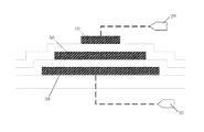
FIG. 4 is a planar view showing the LTPS TFT according to one embodiment of the present invention, and FIG. 5 is a planar view showing the LTPS TFT according to another embodiment of the present invention. In FIG. 4, the guide layers 30 of the LTPS TFTs are arranged separately on the substrate, and thus can be controlled individually. In FIG. 5, the guide layers 30 of the LTPS TFTs are connected to each other on the substrate, and they are connected to a voltage terminal for controlling the voltage applied thereto.
FIG. 6 is a planar view showing the layout of the LTPS TFT when the structure as shown in FIG. 5 is adopted. The shielding metal layers of the display panel form the guide layers 30 of the N-type LTPS TFTs, and all the guide layers 30 on the substrate are connected to each other and grounded respectively. In this embodiment, the shielding metal layers of the display panel are connected to each other, and connected to a grounded end GND of a driving circuit IC60 of the display panel or to a flexible printing circuit board FPC70. The driving circuit IC60 and the flexible printing circuit board FPC70 are both external voltage supply devices for the display panel, and the flexible printing circuit board FPC70 supplies a signal to the driving circuit IC60.
The working principle of the LTPS TFT with the above-mentioned structure will be described hereinafter by taking an N-type LTPS TFT as an example.
In the on state, the gate metal layer 10 is connected to a positive potential, and the guide layer 30, i.e., the shielding metal layer, is connected to the grounded end GND. The electric field formed between the gate metal layer 10 and the semiconductor layer 50 is in a direction as shown in FIG. 7, and the direction is the same as that of the electric field formed between the gate metal layer 10 and the guide layer 30, i.e., it points from the gate metal layer 10 toward the guide layer 30 (both in the vertical and oblique directions). According to the principle that the movement direction of the electrons is opposite to the electric field direction, as compared with the prior art, the additional electric field pointing from the gate metal layer 10 toward the guide layer 30 as shown in FIG. 7 enables the electrons to be more easily accumulated in the semiconductor layer 50 below the gate metal layer 10, thereby it is able to reduce the threshold voltage Vth and increase the on-state current Ion.
In the off state, the gate metal layer 10 is connected to a negative potential, and the guide layer 30, i.e., the shielding metal layer, is connected to the grounded end GND. The electric field formed between the gate metal layer 10 and the semiconductor layer 50 is in a direction as shown in FIG. 8, and the direction is the same as that of the electric field formed between the gate metal layer 10 and the guide layer 30, i.e., it points from the guide layer 30 toward the gate metal layer 10 (both in vertical and oblique directions). According to the principle that the movement direction of the electrons is opposite to the electric field direction, as compared with the prior art, the additional electric field pointing from the guide layer 30 toward the gate metal layer 10 enables the electrons to be more difficultly accumulated below the gate metal layer 10 while the holes to be more easily accumulated below the gate metal layer 10, thereby it is able to reduce the off-state current Ioff through the effect of the electric field.
The above description is given on the basis of the structure of the N-type LTPS TFT and its working principle. Similarly, a P-type LTPS TFT may also be used, the structure and the working principle of which will not be described in detail herein. It should be appreciated that, for the P-type LTPS TFT, the effect of the electric field formed between the shielding metal layer and the gate metal layer is similar to that for the N-type LTPS TFT. In the on state, the gate metal layer attracts the holes due to the effect of the electric field and it is more easily to form the holes below the gate metal layer, thereby it is able to reduce the threshold voltage Vth and increase the on-state current Ion. While in the off state, the gate metal layer repels the holes and attracts the electrons due to the effect of the electric field, thereby it is able to reduce the off-state current Ioff. As a result, it is able to increase the ratio of the on-state current to the off-state current for the LTPS TFT.
In addition, in this embodiment, the shielding metal layer is formed as the guide layer and connected to the grounded end GND. As compared with the shielding metal layer that is free and not connected to a potential, this shield metal layer is less susceptible to an external potential such as charge accumulation, and more helpful for anti-electrostatic discharge (ESD) and anti-electromagnetic interference (EMI).
According to one embodiment of the present invention, the shielding metal layers for shielding the thin film field effect transistor are connected to each other and to the grounded end GND of the IC or FPC. As a result, it is able to reduce the threshold voltage Vth, increase the on-state current Ion and reduce the off-state current Ioff by means of the electric field between the shielding metal layer and the gate metal layer of the thin film field effect transistor, thereby to increase the ratio of the on-state current to the off-state current. In addition, the shielding metal layers, which form a ring, are grounded, and as a result it is able to improve the anti-ESD and anti-EMI performances. Of course, other than materials and processes for the guide layer 30, the materials and processes in the prior art may also be used, and they will not be repeated herein.
The present invention further provides an array substrate on which the above-mentioned thin film field effect transistor is arranged. For example, when the thin film field effect transistor is used as a switch element for a pixel unit of the array substrate, the source metal layer 60 or drain metal layer 70 of the transistor may be connected to a pixel electrode of the pixel unit.
The array substrate comprises a shielding metal layer which forms the guide layer of the thin film field effect transistor.
Further, the shielding metal layer of the array substrate is grounded. In addition, an embodiment of the present invention further provides a display device on which the above-mentioned array substrate is provided. The above-mentioned thin film field effect transistor is arranged on the array substrate of the display device. The display device may be a liquid crystal panel, an electronic paper, an OLED panel, a mobile phone, a tablet PC, a TV, a display, a laptop PC, a digital photo frame, a navigator or any other products or devices having a display function.
The structure of the thin film field effect transistor is mentioned above and will not be repeated herein.
Preferably, when the thin film field effect transistor is an N-type transistor, the shielding metal layers on the display panel form the guide layers, and these shielding metal layers are connected to each other and grounded. Through such a structure, it is able to reduce the threshold voltage Vth, increase the on-state current Ion, reduce the off-state current Ioff, thereby to increase the ratio of the on-state current to the off-state current. Also, it is able to improve the anti-ESD and anti-EMI performances.
An embodiment of the present invention further provides a method for driving the above-mentioned thin film field effect transistor, comprising: when an on-state operating voltage or off-state operating voltage is applied to the gate metal layer to form an electric field between the gate metal layer and the semiconductor layer, applying a predetermined voltage to the guide layer, such that an electric field is also formed between the guide layer and the gate metal layer, the semiconductor layer accumulates electrons or holes to reinforce the electric field between the gate metal layer and the semiconductor layer by utilizing the electric field between the guide layer and the gate metal layer.
Further, the on-state operating voltage is applied to the gate metal layer, and the first voltage is applied to the guide layer, so as to establish an electrical connection between the source metal layer and the drain metal layer, i.e., at this time the predetermined voltage is the first voltage.
The off-state operating voltage is applied to the gate metal layer, and the second voltage is applied to the guide layer, so as to cut off the electrical connection between the source metal layer and the drain metal layer, i.e., at this time, the predetermined voltage is the second voltage.
When the thin film field effect transistor is an N-type transistor, the on-state operating voltage is a positive voltage and the off-state operating voltage is a negative voltage. Either of the first voltage and the second voltage is of a value between the on-state operating voltage and the off-state operating voltage.
When the thin film field effect transistor is a P-type transistor, the on-state operating voltage is a negative voltage and the off-state operating voltage is a positive voltage. Either of the first voltage and the second voltage is of a value between the on-state operating voltage and the off-state operating voltage.
Preferably, the first voltage is equal to the second voltage, and they are both zero. In other words, the predetermined voltage is zero.
An embodiment of the present invention further provides an electronic product comprising the above-mentioned display device. The structure of the display device is mentioned above, and will not be repeated herein.
According to the thin film field effect transistor, driving method thereof, the array substrate, the display device and the electronic product of an embodiment of the present invention, the guide layer is provided, and through the electric field between the guide layer and the gate metal layer when the thin film field effect transistor is in the on state and off state respectively, it is able to reduce the threshold voltage Vth, increase the current Ion when the transistor is turned on and reduce the leakage current Ioff, thereby to affect the current characteristics by improving the structure of the thin film field effect transistor and increase a ratio of the on-state current to the off-state current.
The above are merely the preferred embodiments of the present invention. A person skilled in the art may make further modifications and improvements without departing from the spirit and principle of the present invention, and these modifications and improvements shall also be considered as the protection scope of the present invention.

Claims (17)

What is claimed is:
1. A thin film field effect transistor, comprising a gate metal layer and a semiconductor layer,
wherein the thin film field effect transistor further comprises a guide layer,
wherein when an electric field is formed between the gate metal layer and the semiconductor layer, an electric field is also formed between the guide layer and the gate metal layer, the semiconductor layer accumulates electrons or holes to reinforce the electric field between the gate metal layer and the semiconductor layer by utilizing the electric field between the guide layer and the gate metal layer,
wherein a projection area of the guide layer on a substrate where the thin film field effect transistor is arranged is larger than that of the semiconductor layer, and the projection area of the semiconductor layer on the substrate is larger than that of the gate metal layer, so as to increase an overlapping area between the projection area of the guide layer on the substrate and the projection area of the semiconductor layer on the substrate, and
wherein the guide layer is not in contact with the gate metal layer and wherein the guide layer is disposed over the substrate, the semiconductor layer is disposed over the guide layer, and the gate metal layer is disposed over the semiconductor layer.
2. The thin film field effect transistor according to claim 1, wherein the electric field between the gate metal layer and the guide layer is in a direction identical to the electric field between the gate metal layer and the semiconductor layer.
3. The thin film field effect transistor according to claim 2, wherein when an on-state operating voltage is applied to the gate metal layer, a first voltage is applied to the guide layer, and the electric field between the gate metal layer and the guide layer is in a direction identical to the electric field between the gate metal layer and the semiconductor layer, and
when an off-state operating voltage is applied to the gate metal layer, a second voltage is applied to the guide layer, and the electric field between the gate metal layer and the guide layer is in a direction identical to the electric field between the gate metal layer and the semiconductor layer.
4. The thin film field effect transistor according to claim 3, wherein the thin film field effect transistor is an N-type transistor, the on-state operating voltage is a positive voltage, the off-state operating voltage is a negative voltage, and either of the first voltage and the second voltage is of a value between the on-state operating voltage and the off-state operating voltage.
5. The thin film field effect transistor according to claim 3, wherein the thin film field effect transistor is a P-type transistor, the on-state operating voltage is a negative voltage, the off-state operating voltage is a positive voltage, and either of the first voltage and the second voltage is of a value between the on-state operating voltage and the off-state operating voltage.
6. The thin film field effect transistor according to claim 4, wherein the first voltage is equal to the second voltage, and the first voltage and the second voltage are both zero.
7. The thin film field effect transistor according to claim 1, wherein the semiconductor layer is provided between the gate metal layer and the guide layer.
8. The thin film field effect transistor according to claim 7, wherein a first insulating layer is provided between the semiconductor layer and the gate metal layer, and a second insulating layer is provided between the semiconductor layer and the guide layer.
9. The thin film field effect transistor according to claim 1, wherein the guide layer is made of a conductive material.
10. An array substrate on which the thin film field effect transistor according to claim 1 is provided.
11. The array substrate according to claim 10, wherein the array substrate comprises a shielding metal layer formed as a guide layer.
12. The array substrate according to claim 11, wherein the shielding metal layer is grounded.
13. A display device comprising the array substrate according to claim 10.
14. The thin film field effect transistor according to claim 5, wherein the first voltage is equal to the second voltage, and the first voltage and the second voltage are both zero.
15. A thin film field effect transistor comprising:
a gate metal layer having a first cross section area;
a semiconductor layer having a second cross section area, with the second cross section area being larger than the first cross section area; and
a guide layer having a third cross section area, with the third cross section area being larger than the second cross section area,
wherein when an electric field is formed between the gate metal layer and the semiconductor layer, an electric field is also formed between the guide layer and the gate metal layer, the semiconductor layer accumulates electrons or holes to reinforce the electric field between the gate metal layer and the semiconductor layer by utilizing the electric field between the guide layer and the gate metal layer,
wherein a projection area of the guide layer on a substrate where the thin film field effect transistor is arranged is larger than that of the semiconductor layer and the projection area of the semiconductor layer on the substrate is larger than that of the gate metal layer, so as to increase an overlapping area between the projection area of the guide layer on the substrate and the projection area of the semiconductor layer on the substrate, and
wherein the guide layer is not in contact with the gate metal layer and wherein the guide layer is disposed over the substrate, the semiconductor layer is disposed over the guide layer, and the gate metal layer is disposed over the semiconductor layer.
16. The thin film field effect transistor according to claim 2, wherein the gate metal layer has a first cross section area, the semiconductor layer has a second cross section area, and the guide layer has a third cross section area, the second cross section area being larger than the first cross section area and the third cross section area being larger than the second cross section area.
17. The thin film field effect transistor according to claim 15, wherein the guide layer is disposed between the substrate layer and the semiconductor layer, and the semiconductor layer is disposed between the guide layer and the gate metal layer.
US14/241,558 2013-06-07 2013-08-05 Thin-film field effect transistor, driving method thereof, array substrate, display device, and electronic product Active 2033-11-26 US9515191B2 (en)

Applications Claiming Priority (4)

Application Number Priority Date Filing Date Title
CN201310226377.4 2013-06-07
CN2013102263774A CN103311312A (en) 2013-06-07 2013-06-07 Thin-film field-effect transistor and drive method thereof, array substrate, and display device
CN201310226377 2013-06-07
PCT/CN2013/080789 WO2014194558A1 (en) 2013-06-07 2013-08-05 Thin-film field-effect transistor and driving method thereof, array substrate, display device, and electronic product

Publications (2)

Publication Number Publication Date
US20150311344A1 US20150311344A1 (en) 2015-10-29
US9515191B2 true US9515191B2 (en) 2016-12-06

Family

ID=49136324

Family Applications (1)

Application Number Title Priority Date Filing Date
US14/241,558 Active 2033-11-26 US9515191B2 (en) 2013-06-07 2013-08-05 Thin-film field effect transistor, driving method thereof, array substrate, display device, and electronic product

Country Status (3)

Country Link
US (1) US9515191B2 (en)
CN (1) CN103311312A (en)
WO (1) WO2014194558A1 (en)

Families Citing this family (6)

* Cited by examiner, † Cited by third party
Publication number Priority date Publication date Assignee Title
US9721845B1 (en) * 2016-04-26 2017-08-01 International Business Machines Corporation Vertical field effect transistors with bottom contact metal directly beneath fins
JP2017207744A (en) * 2016-05-11 2017-11-24 株式会社半導体エネルギー研究所 Display device, module, and electronic device
CN107664891A (en) * 2017-10-26 2018-02-06 京东方科技集团股份有限公司 A kind of array base palte, its preparation method, display panel and display device
CN107958922B (en) * 2017-12-11 2020-06-30 京东方科技集团股份有限公司 Display substrate, manufacturing method thereof and display panel
CN112103339A (en) * 2020-09-03 2020-12-18 Oppo广东移动通信有限公司 Thin film transistor, pixel circuit, display panel, and electronic device
CN113257837A (en) * 2021-05-11 2021-08-13 京东方科技集团股份有限公司 Flexible display substrate, display device and preparation method

Citations (11)

* Cited by examiner, † Cited by third party
Publication number Priority date Publication date Assignee Title
JPH04334061A (en) 1991-05-09 1992-11-20 Fujitsu Ltd Thin film transistor matrix and its manufacture
JPH08107212A (en) 1994-10-06 1996-04-23 Fujitsu Ltd Thin film transistor matrix substrate and its manufacture
US5831707A (en) * 1994-08-24 1998-11-03 Hitachi, Ltd. Active matrix type liquid crystal display apparatus
US20030038288A1 (en) 2001-08-16 2003-02-27 International Business Machines Corporation Thin film transistor and method of making same
US20030075733A1 (en) * 2001-09-10 2003-04-24 Semiconductor Energy Laboratory Co., Ltd. Light emitting device and method of manufacturing a semiconductor device
CN1480914A (en) 1998-11-26 2004-03-10 精工爱普生株式会社 Electrooptical device, its mfg. method and electronic device
US20050282317A1 (en) * 2000-03-29 2005-12-22 Sony Corporation Thin film semiconductor apparatus and method for driving the same
JP2006165233A (en) 2004-12-07 2006-06-22 Canon Inc Organic electronic device and method for preparing it
CN1797151A (en) 2004-12-31 2006-07-05 Lg.菲利浦Lcd株式会社 Liquid crystal display device and manufacturing method thereof
CN101595567A (en) 2007-01-10 2009-12-02 索尼株式会社 Semiconductor device and display unit
US20110175674A1 (en) 2010-01-15 2011-07-21 Canon Kabushiki Kaisha Method of driving transistor and device including transistor driven by the method

Family Cites Families (1)

* Cited by examiner, † Cited by third party
Publication number Priority date Publication date Assignee Title
CN102969362B (en) * 2011-09-01 2016-03-30 中国科学院微电子研究所 high stability amorphous metal oxide TFT device

Patent Citations (12)

* Cited by examiner, † Cited by third party
Publication number Priority date Publication date Assignee Title
JPH04334061A (en) 1991-05-09 1992-11-20 Fujitsu Ltd Thin film transistor matrix and its manufacture
US5831707A (en) * 1994-08-24 1998-11-03 Hitachi, Ltd. Active matrix type liquid crystal display apparatus
JPH08107212A (en) 1994-10-06 1996-04-23 Fujitsu Ltd Thin film transistor matrix substrate and its manufacture
CN1480914A (en) 1998-11-26 2004-03-10 精工爱普生株式会社 Electrooptical device, its mfg. method and electronic device
US20050282317A1 (en) * 2000-03-29 2005-12-22 Sony Corporation Thin film semiconductor apparatus and method for driving the same
US20030038288A1 (en) 2001-08-16 2003-02-27 International Business Machines Corporation Thin film transistor and method of making same
US20030075733A1 (en) * 2001-09-10 2003-04-24 Semiconductor Energy Laboratory Co., Ltd. Light emitting device and method of manufacturing a semiconductor device
JP2006165233A (en) 2004-12-07 2006-06-22 Canon Inc Organic electronic device and method for preparing it
CN1797151A (en) 2004-12-31 2006-07-05 Lg.菲利浦Lcd株式会社 Liquid crystal display device and manufacturing method thereof
US7679699B2 (en) 2004-12-31 2010-03-16 Lg Display Co., Ltd. Liquid crystal display device and fabricating method thereof
CN101595567A (en) 2007-01-10 2009-12-02 索尼株式会社 Semiconductor device and display unit
US20110175674A1 (en) 2010-01-15 2011-07-21 Canon Kabushiki Kaisha Method of driving transistor and device including transistor driven by the method

Non-Patent Citations (7)

* Cited by examiner, † Cited by third party
Title
Chinese Office Action for Chinese Application No. 201310226377.4, dated Sep. 28, 2016, 5 Pages.
Chinese Office Action of corresponding CN 201310226377.4 dated Apr. 3, 2015; 4 pages [English Tranlsation].
Chinese Office Action of corresponding CN 201310226377.4 dated Apr. 3, 2015; 7 pages.
Chinese Second Office Action Dated Sep. 30, 2015, Application No. 201310226377.4, 4 Pages.
Chinese Third Office Action Dated Apr. 1, 2016, Application No. 201310226377.4, 5 Pages.
English Translation of PCT Written Opinion of the International Searching Authority, Application PCT/CN2013/080789, 3 Pages.
PCT/CN2013/080789 Search Report and Written Opinion; dated: Mar. 20, 2014; 12 pages.

Also Published As

Publication number Publication date
CN103311312A (en) 2013-09-18
WO2014194558A1 (en) 2014-12-11
US20150311344A1 (en) 2015-10-29

Similar Documents

Publication Publication Date Title
CN108155195B (en) Display device
CN109427817B (en) Thin film transistor substrate and display
US9515191B2 (en) Thin-film field effect transistor, driving method thereof, array substrate, display device, and electronic product
US9299761B2 (en) Organic light emitting display device and method of manufacturing the same
US10276607B2 (en) Display panel, manufacturing method thereof and display device
US9947691B2 (en) Array substrate, manufacturing method thereof and display panel
US20180151659A1 (en) Semiconductor device, display unit, method of manufacturing display unit, and electronic apparatus
US8304778B2 (en) Thin film transistor and pixel structure having the thin film transistor
US11264507B2 (en) Thin film transistor and method for manufacturing the same, array substrate and electronic device
US9818772B2 (en) Display device and method for manufacturing the same
US11158628B2 (en) Electro-static discharge circuit, array substrate, display panel and display apparatus
US20230086999A1 (en) Gate driving circuit and manufacturing method therefor, array substrate, and display device
WO2024011951A1 (en) Display panel and display apparatus
CN111415995B (en) Display panel, manufacturing method thereof and display device
EP3683846A1 (en) Thin film transistor and manufacturing method therefor, and electronic apparatus
US20170033236A1 (en) Thin-film transistor structure
WO2024011947A1 (en) Display panel and display apparatus
CN105097898B (en) Thin film transistor, array substrate and display device
US11664389B2 (en) Thin film transistor substrate and display device
US20190097063A1 (en) Esl tft substrate and fabrication method thereof
CN115172385A (en) Array substrate and display panel
JP2015170642A (en) display device
CN113433747A (en) Array substrate, manufacturing method and mobile terminal
US9082664B2 (en) Method for manufacturing thin-film transistor substrate and thin-film transistor substrate manufactured with same
JP2015056565A (en) Thin film transistor, display device electrode substrate and manufacturing methods of those

Legal Events

Date Code Title Description
AS Assignment

Owner name: CHENGDU BOE OPTOELECTRONICS TECHNOLOGY CO., LTD.,

Free format text: ASSIGNMENT OF ASSIGNORS INTEREST;ASSIGNORS:WU, BO;QI, XIAOJING;REEL/FRAME:032312/0837

Effective date: 20140217

Owner name: BOE TECHNOLOGY GROUP CO., LTD., CHINA

Free format text: ASSIGNMENT OF ASSIGNORS INTEREST;ASSIGNORS:WU, BO;QI, XIAOJING;REEL/FRAME:032312/0837

Effective date: 20140217

STCF Information on status: patent grant

Free format text: PATENTED CASE

MAFP Maintenance fee payment

Free format text: PAYMENT OF MAINTENANCE FEE, 4TH YEAR, LARGE ENTITY (ORIGINAL EVENT CODE: M1551); ENTITY STATUS OF PATENT OWNER: LARGE ENTITY

Year of fee payment: 4