US9515399B2 - Connector alignment system - Google Patents
Connector alignment system Download PDFInfo
- Publication number
- US9515399B2 US9515399B2 US15/094,747 US201615094747A US9515399B2 US 9515399 B2 US9515399 B2 US 9515399B2 US 201615094747 A US201615094747 A US 201615094747A US 9515399 B2 US9515399 B2 US 9515399B2
- Authority
- US
- United States
- Prior art keywords
- component
- connector
- board
- subsystem
- alignment
- Prior art date
- Legal status (The legal status is an assumption and is not a legal conclusion. Google has not performed a legal analysis and makes no representation as to the accuracy of the status listed.)
- Active
Links
Images


Classifications
-
- H—ELECTRICITY
- H01—ELECTRIC ELEMENTS
- H01R—ELECTRICALLY-CONDUCTIVE CONNECTIONS; STRUCTURAL ASSOCIATIONS OF A PLURALITY OF MUTUALLY-INSULATED ELECTRICAL CONNECTING ELEMENTS; COUPLING DEVICES; CURRENT COLLECTORS
- H01R12/00—Structural associations of a plurality of mutually-insulated electrical connecting elements, specially adapted for printed circuits, e.g. printed circuit boards [PCB], flat or ribbon cables, or like generally planar structures, e.g. terminal strips, terminal blocks; Coupling devices specially adapted for printed circuits, flat or ribbon cables, or like generally planar structures; Terminals specially adapted for contact with, or insertion into, printed circuits, flat or ribbon cables, or like generally planar structures
- H01R12/70—Coupling devices
- H01R12/7005—Guiding, mounting, polarizing or locking means; Extractors
-
- G—PHYSICS
- G06—COMPUTING; CALCULATING OR COUNTING
- G06F—ELECTRIC DIGITAL DATA PROCESSING
- G06F1/00—Details not covered by groups G06F3/00 - G06F13/00 and G06F21/00
- G06F1/16—Constructional details or arrangements
- G06F1/18—Packaging or power distribution
- G06F1/183—Internal mounting support structures, e.g. for printed circuit boards, internal connecting means
- G06F1/185—Mounting of expansion boards
-
- H—ELECTRICITY
- H01—ELECTRIC ELEMENTS
- H01R—ELECTRICALLY-CONDUCTIVE CONNECTIONS; STRUCTURAL ASSOCIATIONS OF A PLURALITY OF MUTUALLY-INSULATED ELECTRICAL CONNECTING ELEMENTS; COUPLING DEVICES; CURRENT COLLECTORS
- H01R12/00—Structural associations of a plurality of mutually-insulated electrical connecting elements, specially adapted for printed circuits, e.g. printed circuit boards [PCB], flat or ribbon cables, or like generally planar structures, e.g. terminal strips, terminal blocks; Coupling devices specially adapted for printed circuits, flat or ribbon cables, or like generally planar structures; Terminals specially adapted for contact with, or insertion into, printed circuits, flat or ribbon cables, or like generally planar structures
- H01R12/70—Coupling devices
- H01R12/71—Coupling devices for rigid printing circuits or like structures
- H01R12/72—Coupling devices for rigid printing circuits or like structures coupling with the edge of the rigid printed circuits or like structures
- H01R12/722—Coupling devices for rigid printing circuits or like structures coupling with the edge of the rigid printed circuits or like structures coupling devices mounted on the edge of the printed circuits
-
- H—ELECTRICITY
- H05—ELECTRIC TECHNIQUES NOT OTHERWISE PROVIDED FOR
- H05K—PRINTED CIRCUITS; CASINGS OR CONSTRUCTIONAL DETAILS OF ELECTRIC APPARATUS; MANUFACTURE OF ASSEMBLAGES OF ELECTRICAL COMPONENTS
- H05K3/00—Apparatus or processes for manufacturing printed circuits
- H05K3/30—Assembling printed circuits with electric components, e.g. with resistor
- H05K3/301—Assembling printed circuits with electric components, e.g. with resistor by means of a mounting structure
-
- H—ELECTRICITY
- H05—ELECTRIC TECHNIQUES NOT OTHERWISE PROVIDED FOR
- H05K—PRINTED CIRCUITS; CASINGS OR CONSTRUCTIONAL DETAILS OF ELECTRIC APPARATUS; MANUFACTURE OF ASSEMBLAGES OF ELECTRICAL COMPONENTS
- H05K7/00—Constructional details common to different types of electric apparatus
- H05K7/14—Mounting supporting structure in casing or on frame or rack
- H05K7/1417—Mounting supporting structure in casing or on frame or rack having securing means for mounting boards, plates or wiring boards
- H05K7/1418—Card guides, e.g. grooves
-
- H—ELECTRICITY
- H05—ELECTRIC TECHNIQUES NOT OTHERWISE PROVIDED FOR
- H05K—PRINTED CIRCUITS; CASINGS OR CONSTRUCTIONAL DETAILS OF ELECTRIC APPARATUS; MANUFACTURE OF ASSEMBLAGES OF ELECTRICAL COMPONENTS
- H05K7/00—Constructional details common to different types of electric apparatus
- H05K7/14—Mounting supporting structure in casing or on frame or rack
- H05K7/1422—Printed circuit boards receptacles, e.g. stacked structures, electronic circuit modules or box like frames
- H05K7/1435—Expandable constructions
-
- H—ELECTRICITY
- H01—ELECTRIC ELEMENTS
- H01R—ELECTRICALLY-CONDUCTIVE CONNECTIONS; STRUCTURAL ASSOCIATIONS OF A PLURALITY OF MUTUALLY-INSULATED ELECTRICAL CONNECTING ELEMENTS; COUPLING DEVICES; CURRENT COLLECTORS
- H01R12/00—Structural associations of a plurality of mutually-insulated electrical connecting elements, specially adapted for printed circuits, e.g. printed circuit boards [PCB], flat or ribbon cables, or like generally planar structures, e.g. terminal strips, terminal blocks; Coupling devices specially adapted for printed circuits, flat or ribbon cables, or like generally planar structures; Terminals specially adapted for contact with, or insertion into, printed circuits, flat or ribbon cables, or like generally planar structures
- H01R12/70—Coupling devices
- H01R12/71—Coupling devices for rigid printing circuits or like structures
- H01R12/712—Coupling devices for rigid printing circuits or like structures co-operating with the surface of the printed circuit or with a coupling device exclusively provided on the surface of the printed circuit
- H01R12/714—Coupling devices for rigid printing circuits or like structures co-operating with the surface of the printed circuit or with a coupling device exclusively provided on the surface of the printed circuit with contacts abutting directly the printed circuit; Button contacts therefore provided on the printed circuit
-
- H—ELECTRICITY
- H05—ELECTRIC TECHNIQUES NOT OTHERWISE PROVIDED FOR
- H05K—PRINTED CIRCUITS; CASINGS OR CONSTRUCTIONAL DETAILS OF ELECTRIC APPARATUS; MANUFACTURE OF ASSEMBLAGES OF ELECTRICAL COMPONENTS
- H05K2201/00—Indexing scheme relating to printed circuits covered by H05K1/00
- H05K2201/10—Details of components or other objects attached to or integrated in a printed circuit board
- H05K2201/10007—Types of components
- H05K2201/10189—Non-printed connector
-
- H—ELECTRICITY
- H05—ELECTRIC TECHNIQUES NOT OTHERWISE PROVIDED FOR
- H05K—PRINTED CIRCUITS; CASINGS OR CONSTRUCTIONAL DETAILS OF ELECTRIC APPARATUS; MANUFACTURE OF ASSEMBLAGES OF ELECTRICAL COMPONENTS
- H05K2203/00—Indexing scheme relating to apparatus or processes for manufacturing printed circuits covered by H05K3/00
- H05K2203/16—Inspection; Monitoring; Aligning
- H05K2203/167—Using mechanical means for positioning, alignment or registration, e.g. using rod-in-hole alignment
Definitions
- the present disclosure relates generally to information handling systems, and more particularly to an alignment system for connectors.
- IHS information handling system
- An IHS generally processes, compiles, stores, and/or communicates information or data for business, personal, or other purposes. Because technology and information handling needs and requirements may vary between different applications, IHSs may also vary regarding what information is handled, how the information is handled, how much information is processed, stored, or communicated, and how quickly and efficiently the information may be processed, stored, or communicated. The variations in IHSs allow for IHSs to be general or configured for a specific user or specific use such as financial transaction processing, airline reservations, enterprise data storage, or global communications. In addition, IHSs may include a variety of hardware and software components that may be configured to process, store, and communicate information and may include one or more computer systems, data storage systems, and networking systems.
- a circuit board may include a first connector
- a mezzanine card may include a plurality of second connectors
- a cable may include a third connector
- a stacked connector system is provided when one of the second connectors on the mezzanine card is connected to the first connector on the circuit board, and the third connector on the cable is connected to the other of the second connectors on the mezzanine card.
- it can be difficult to align the one of the second connectors on the mezzanine card and the first connector on the circuit board, and/or align the third connector on the cable and the other of the second connectors on the mezzanine card. Misalignment of connectors in the connector system can result in limited functionality in the IHS, damage to connectors, damage to other components in the IHS, and/or a variety of other problems known in the art.
- a connector alignment system includes a base member that defines a board connector channel and that includes at least one board mounting feature that is configured to mount the base member to a board that includes a board connector such that the board connector is located immediately adjacent the board connector channel; a plurality of first alignment members that extend from the base member on opposite sides of the board connector channel, wherein the plurality of first alignment members define a first alignment channel that is configured to align a primary first component connector on a first component with the board connector along a first axis when the base member is mounted to the board; and a plurality of second alignment members that extend from the base member in a spaced apart relationship from the plurality of first alignment members, wherein the plurality of second alignment members define a second alignment channel that is configured to align a second component connector on a second component with a secondary first component connector on the first component along the first axis when the primary first component connector on the first component is connected to the board connector.
- FIG. 1 is a schematic view illustrating an embodiment of an information handling system.
- FIG. 2 is a perspective view illustrating an embodiment of a circuit board.
- FIG. 3 a is a perspective view illustrating an embodiment of an alignment element.
- FIG. 3 b is a front view illustrating an embodiment of the alignment element of FIG. 3 a
- FIG. 3 c is a top view illustrating an embodiment of the alignment element of FIG. 3 a.
- FIG. 3 d is a rear illustrating an embodiment of the alignment element of FIG. 3 a.
- FIG. 4 a is a top view illustrating an embodiment of a card.
- FIG. 4 b is a front view illustrating an embodiment of the card of FIG. 4 a.
- FIG. 4 c is a bottom view illustrating an embodiment of the card of FIG. 4 a.
- FIG. 5 a is a top view illustrating an embodiment of a cabling system.
- FIG. 5 b is a front view illustrating an embodiment of the cabling system of FIG. 5 a.
- FIG. 5 c is a bottom view illustrating an embodiment of the cabling system of FIG. 5 a.
- FIG. 6 is a flow chart illustrating an embodiment of a method for aligning connectors.
- FIG. 7 a is a perspective view illustrating an embodiment of the alignment element of FIGS. 3 a -3 d coupled to the circuit board of FIG. 2 .
- FIG. 7 b is a top view illustrating an embodiment of the alignment element and the circuit board of FIG. 7 a.
- FIG. 8 is a perspective view illustrating an embodiment of the card of FIGS. 4 a -4 c being connected to the circuit board of FIG. 2 using the alignment element of FIGS. 3 a - 3 d.
- FIG. 9 is a perspective view illustrating an embodiment of the cable of FIGS. 5 a and 5 b being connected to the connected card and circuit board of FIG. 8 using the alignment element of FIGS. 3 a - 3 d.
- an IHS may include any instrumentality or aggregate of instrumentalities operable to compute, classify, process, transmit, receive, retrieve, originate, switch, store, display, manifest, detect, record, reproduce, handle, or utilize any form of information, intelligence, or data for business, scientific, control, entertainment, or other purposes.
- an IHS may be a personal computer, a PDA, a consumer electronic device, a display device or monitor, a network server or storage device, a switch router or other network communication device, or any other suitable device and may vary in size, shape, performance, functionality, and price.
- the IHS may include memory, one or more processing resources such as a central processing unit (CPU) or hardware or software control logic.
- CPU central processing unit
- Additional components of the IHS may include one or more storage devices, one or more communications ports for communicating with external devices as well as various input and output (I/O) devices, such as a keyboard, a mouse, and a video display.
- the IHS may also include one or more buses operable to transmit communications between the various hardware components.
- IHS 100 includes a processor 102 , which is connected to a bus 104 .
- Bus 104 serves as a connection between processor 102 and other components of IHS 100 .
- An input device 106 is coupled to processor 102 to provide input to processor 102 .
- Examples of input devices may include keyboards, touchscreens, pointing devices such as mouses, trackballs, and trackpads, and/or a variety of other input devices known in the art.
- Programs and data are stored on a mass storage device 108 , which is coupled to processor 102 . Examples of mass storage devices may include hard discs, optical disks, magneto-optical discs, solid-state storage devices, and/or a variety other mass storage devices known in the art.
- IHS 100 further includes a display 110 , which is coupled to processor 102 by a video controller 112 .
- a system memory 114 is coupled to processor 102 to provide the processor with fast storage to facilitate execution of computer programs by processor 102 .
- Examples of system memory may include random access memory (RAM) devices such as dynamic RAM (DRAM), synchronous DRAM (SDRAM), solid state memory devices, and/or a variety of other memory devices known in the art.
- RAM random access memory
- DRAM dynamic RAM
- SDRAM synchronous DRAM
- solid state memory devices solid state memory devices
- a chassis 116 houses some or all of the components of IHS 100 . It should be understood that other buses and intermediate circuits can be deployed between the components described above and processor 102 to facilitate interconnection between the components and the processor 102 .
- the board 200 may be a variety of circuit boards known in the art such as, for example, a motherboard that may be housed in the IHS 100 discussed above with reference to FIG. 1 .
- the board connector 202 may be a board connector that is configured to electrically couple with a compression connector, discussed in further detail below. While the board connector 202 is illustrated as raised from the board 200 for clarity of illustration and discussion, the board connector 202 may simply include connector pads 204 that are provided on the board 200 and that are coupled to traces in the board 200 . As such, the board connector may be integral to the board 200 rather than including a separate connector that has been attached to the board 200 .
- the board connector 202 (and/or the board 200 ) also defines first board retention channels 206 that are located on opposite sides of the connector pads 204 and that may be threaded or include other features for securing to a retention member, discussed in further detail below.
- the board 200 also defines second board retention channels 208 that are located on opposite sides of the board connector 202 and that may be threaded or include other features for securing to a retention member, discussed in further detail below.
- the board 200 may couple to a variety of IHS components known in the art including, for example, the processor 102 and the system memory 114 discussed above with reference to FIG. 1 , and thus the board connector 202 (e.g., the connector pads 204 ) may be coupled to those IHS components through the board 200 .
- the board 200 , board connector 202 , and/or other board features may be provided as part of a stacked compression connector system described in U.S. patent application Ser. No. 14/467,807, attorney docket number 102450.00152, filed on Aug. 25, 2014, the disclosure of which is incorporated by reference herein in its entirety.
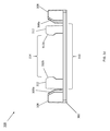
- the alignment element 300 includes a base member 302 that defines a board connector channel 304 .
- the base member 302 also defines a plurality of board mounting features 306 that are located on opposite sides of the board connector channel 304 and that may be threaded or include other features for securing to a retention member, discussed in further detail below.
- a plurality of first alignment members 308 extend from the base member 302 on opposite sides of the board connector channel 304 and define a first alignment channel 310 between them.
- Each of the plurality of first alignment members 308 include a beveled edge 308 a that is located adjacent the first alignment channel 310 .
- a plurality of second alignment members 312 extend from the base member 302 in a spaced apart relationship along an edge of the board connector channel 304 and define a second alignment channel 314 between them.
- the plurality of second alignment members 312 provide a first set of beveled edges 312 a adjacent the board connector channel 304 , and provide a second set of beveled edges 312 b adjacent the second alignment channel 314 .
- the first component 400 is a card such as, for example, mezzanine card.
- the mezzanine card illustrated in FIGS. 4 a -4 c may be a storage mezzanine card such as a Redundant Array of Independent Disks (RAID) mezzanine card.
- RAID Redundant Array of Independent Disks
- the first component 400 includes a card base 402 that may be a circuit board including a variety of card components that have not been illustrated for clarity but that may include processing systems, memory systems, storage systems, heat dissipation devices, and/or a variety of other card components known in the art.
- the card base 402 includes a top side 402 a , a bottom side 402 b that is located opposite the card base 402 from the top side 402 a , and a front edge 402 c that extends between the top side 402 a and the bottom side 402 b .
- a primary first component connector 404 is located on the bottom side 402 b of the card base 402 and adjacent the front edge 402 c of the card base 402 .
- the primary first component connector 404 may be a compression connector.
- the primary first component connector 404 includes a plurality of connector pins 406 and a plurality of primary connector retention channels 408 that are located on opposite sides of the plurality of connector pins 406 .
- a secondary first component connector 410 is located on the top side 402 a of the card base 402 and adjacent the front edge 402 c of the card base 402 .
- the secondary first component connector 410 may be a compression connector.
- the secondary first component connector 410 includes a plurality of connector pins 412 , a plurality of primary connector retention channels 414 that are located on opposite sides of the plurality of connector pins 412 , and a plurality of guide members 416 that extend from the primary first component connector 410 on opposite sides of the plurality of connector pins 412 and the plurality of primary connector retention channels 414 .
- a connector protector 415 (omitted in FIG.
- the card base 402 may define card base retention channels that align with the primary connector retention channels 408 and the secondary connector retention channels 414 to provide first component retention channels that extend through the primary first component connector 404 , the card base 402 , and the secondary first component connector 410 .
- the primary first component connector 404 and the secondary first component connector 410 may each be coupled through the board 402 (e.g., via traces) to a processing system on the board 402 that may operate to, for example, convert signals passing between the primary first component connector 404 and the secondary first component connector 410 and/or perform a variety of other processing functions known in the art.
- the first component may be provided as part of a stacked compression connector system described in U.S. patent application Ser. No. 14/467,807, attorney docket number 102450.00152, filed on Aug. 25, 2014, the disclosure of which is incorporated by reference herein in its entirety.
- the primary first component connector 404 may be directly aligned with the secondary first component connector 410 on opposite sides of the board 402 .
- the second component 500 includes cabling 502 that extends from a cabling base 504 .
- a second component connector 506 extends from the cabling base 504 opposite the cabling base 504 from the cabling 502 .
- the second component connector 506 includes a top side 506 a and a bottom side 506 b that is located opposite the second component connector 506 from the top side 506 a .
- a plurality of connector pads 508 are located on the bottom side 506 b of the second component connector 506 .
- a plurality of retention members 510 are coupled to the second component connector 506 such that the each retention member 510 extends from both the top side 506 a and the bottom side 506 b of the second component connector 506 .
- the second component connector 506 defines a plurality of guide channels 512 that are located on opposite sides of the plurality of connector pads 508 and the plurality of retention members 510 .
- a plurality of second component alignment channels 514 are defined by the cabling base 504 and second component connector 506 and are located opposite the plurality of connector pads 508 from each other.
- the cabling system 500 may be provided as part of a stacked compression connector system described in U.S. patent application Ser. No. 14/467,807, filed on Aug. 25, 2014, the disclosure of which is incorporated by reference herein in its entirety.
- the method 600 begins at block 602 where a connector alignment system is provided.
- the alignment element 300 discussed above with reference to FIGS. 3 a - d is mounted to the board 200 discussed above with reference to FIG. 2 to provide the connector alignment system 700 illustrated in FIGS. 7 a and 7 b .
- the alignment element 200 is positioned adjacent the board 200 such that the board mounting features 306 defined by the base member 302 are aligned with the second board retention features 208 defined by the board 200 , and the board connector 202 on the board 200 is located adjacent the board connector channel 304 defined by the base member 302 .
- Retention members 702 e.g., screws in the illustrated embodiment
- the orientation of the alignment element 300 relative to the board 200 may be selected by the user based on the desired connection orientations of the first component 400 and/or the second component 500 .
- guide features/retention members 704 have been positioned in the first board retention channels 206 on the board 200 .
- the guide features/retention members 704 may be omitted from the connector alignment system 700 while remaining from the scope of the present disclosure.
- the method 600 then proceeds to block 604 where a first component is engaged with first alignment members to align a primary first component connector with a board connector.
- the first component 400 discussed above with reference to FIGS. 4 a -4 c may be positioned adjacent the alignment element 300 such that the bottom side 402 b of the card base 402 faces the board 200 and the primary first component connector 404 is located adjacent the board connector 202 , as illustrated in FIG. 8 .
- the first component 400 may then be moved in a direction A relative to and towards the board 200 .
- one or more edges of the board 200 adjacent the front edge 402 c may engage one or more of the first alignment members 308 on the alignment element 300 to enter the first alignment channel 310 .
- the one or more edges of the board 200 adjacent the front edge 402 c may engage the beveled edges 308 a on the one or more first alignment members 308 in response to the movement in direction A, which channels the first component 400 into the first alignment channel 304 such that the primary first component connector 404 is aligned with the board connector 202 along a first axis B.
- the connector protector 415 (or the front edge 402 c of the card base 402 when no connector protector 415 is provided) may engage one or more of the second alignment members 312 on the alignment element 300 .
- the connector protector 415 (or the front edge 402 c of the board 200 ) may engage the first set of beveled edges 312 a on the one or more second alignment members 312 in response to the movement in direction A, which operates to align the primary first component connector 404 with the board connector 202 along a second axis C.
- first alignment members 308 and/or the second alignment members 312 may include detents (e.g., below the beveled edges 308 a on the first alignment members 308 , and below the first set of beveled edges 312 a on the second alignment members 312 ) that may operate to hold the first component 400 in an aligned position engaging the alignment element 300 after moving a sufficient distance in the direction A.
- detents e.g., below the beveled edges 308 a on the first alignment members 308 , and below the first set of beveled edges 312 a on the second alignment members 312 .
- the positioning of the first component 400 adjacent the alignment element 300 and movement in the direction A operates to align the primary first component connector 404 with the board connector 202 along two axes (e.g., the first axis B and the second axis C in the illustrated embodiment). Alignment of the primary first component connector 404 and the board connector 202 along these two axes operates to align the connector pins 406 on the primary first component connector 404 with the connector pads 204 on the board connector 202 , as well as to align the first component retention channels on the first component 400 with the first board retention channels 206 (and in some embodiment, the guide features/retention members 704 ) on the board connector 202 .
- the method 600 proceeds to block 606 where the primary first component connector is connected to the board connector.
- Continued movement of the first component 400 in the direction A causes the primary first component connector 404 to engage the board connector 202 , with the first alignment members 308 /first alignment channel 310 and the second alignment members 312 ensuring that the connector pins 406 on the primary first component connector 404 are properly aligned with the connector pads 204 on the board connector 202 for mating, engagement, or otherwise being electrically connected.
- the continued movement of the first component 400 in the direction A causes the guide features/retention members 704 to enter the first component retention channels on the first component 400 to further ensure proper alignment of the connector pins 406 and the connector pads 204 .
- the alignment element 400 may negate the need for the guide features/retention members 704 to perform the alignment process.
- the connector alignment system 700 operates to ensure alignment of the connector pins 406 and the connector pads 204 on the primary first component connector 404 and the board connector 202 , respectively, in order to prevent possible damage that may occur in response to an attempt to connect them in an unaligned state.
- a latch may be included on the alignment element 300 and configured to extend across the alignment element 300 and into engagement with the first component 400 in order to provide a load on the first component 400 that ensures an electrical connection between the primary first component connector 404 and the board connector 202 .
- the method 600 then proceeds to block 608 where a second component is engaged with second alignment members to align a second component connector with a secondary first component connector.
- the second component 500 discussed above with reference to FIGS. 5 a -5 c may be positioned adjacent the alignment element 300 such that the bottom side 506 b of the second component connector 506 faces the board 200 , the second component connector 506 is located adjacent the secondary first component connector 410 on the first component 400 , and the second component alignment channels 514 on the second component 500 are aligned with the second alignment members 512 , as illustrated in FIG. 9 .
- the second component 500 may then be moved in a direction D relative to and towards the board 200 .
- the second alignment members 312 on the alignment element 300 enter the second component alignment channels 514 on the second component 500
- the second component connector 506 engages one or more of the second alignment members 312
- the second component 500 enters the second alignment channel 314 .
- portions of the cabling base 504 and the second component connector 506 that define the second component alignment channels 514 may engage the second set of beveled edges 312 a on the one or more second alignment members 312 in response to the movement in direction D, which channels the second component 500 into the second alignment channel 314 such that the second component connector 506 is aligned with the secondary first component connector 410 along the first axis B.
- portions of the cabling base 504 and the second component connector 506 that define the second component alignment channels 514 may engage the second set of beveled edges 312 a on the one or more second alignment members 312 in response to the movement in direction D, which operates to align the second component connector 506 with the secondary first component connector 410 along the second axis C.
- the second alignment members 312 may include detents (e.g., below the first set of beveled edges 312 a and/or the second set of beveled edges 312 b on the second alignment members 312 ) that may operate to hold the second component 500 in an aligned position engaging the alignment element 300 after moving a sufficient distance in the direction D.
- detents e.g., below the first set of beveled edges 312 a and/or the second set of beveled edges 312 b on the second alignment members 312 .
- the positioning of the second component 500 adjacent the alignment element 300 and movement in the direction D operates to align the second component connector 506 with the secondary first component connector 410 along two axes (e.g., the first axis B and the second axis C in the illustrated embodiment). Alignment of the second component connector 506 and the secondary first component connector 410 along these two axes operates to align the connector pads 508 on the second component connector 506 with the connector pins 412 on the secondary first component connector 410 , to align the first component retention channels on the first component 400 with the retention members 510 on the second component connector 506 , and to align the guide members 416 on the secondary first component connector 410 with the guide channels 512 on the second component connector 506 .
- the method 600 proceeds to block 610 where the second component connector is connected to the secondary first component connector.
- Continued movement of the second component 500 in the direction D causes the second component connector 506 to engage the secondary first component connector 410 , with the second alignment members 312 /second alignment channel 314 ensuring that the connector pins 412 on the secondary first component connector 410 are properly aligned with the connector pads 508 on the second component connector 506 for mating, engagement, or otherwise being electrically connected.
- the continued movement of the second component 500 in the direction D causes the guide members 416 to enter the guide channels 512 on the second component connector 506 to further ensure proper alignment of the connector pins 412 and the connector pads 508 .
- the guide members 416 may be omitted, and only the alignment element 300 may operate to align the second component connector 506 and the secondary first component connector 410 .
- the connector alignment system 700 operates to ensure alignment of the connector pins 412 and the connector pads 508 on the second component connector 506 and the secondary first component connector 410 , respectively, in order to prevent possible damage that may occur in response to an attempt to connect them in an unaligned state.
- the retention members 510 Upon engaging the second component connector 506 and the secondary first component connector 410 , the retention members 510 extend through the first component retention channels defined by the first component 400 , and may be engaged with the first board retention channels 206 to secure both the first component 400 and the second component 500 to the board 200 and to ensure mating, engagement, and/or electrical connection of the primary first component connector 404 with the board connector 202 and of the secondary first component connector 410 with the second component connector 506 .
- a latch may be included on the alignment element 300 and configured to extend across the alignment element 300 and into engagement with the second component 500 in order to provide a load on the second component 500 that ensures an electrical connection between the second component connector 506 and the secondary first component connector 410 and/or the primary first component connector 404 and the board connector 202 .
- the connector alignment systems and methods of the present disclosure provide an alignment element that provides for the alignment of multiple components that include compression connectors that are presented to other compression connectors from different directions using alignment members that provide for the alignment of those components along multiple axes. While the embodiments illustrated and described above includes only two stacked components (the first component 400 and the second component 500 ), additional components with similar compression connectors may be provided, aligned, and connected in substantially the same manner using the alignment element (or similar alignment elements) while remaining within the scope of the present disclosure.
- a third component with compression connectors similar to those on the first component may be aligned with and connected to the compression connectors on the first component
- a fourth component with compression connectors similar to those on the first component may be aligned with and connected to the compression connectors on the third component
- the second component may be aligned with and connected to the compression connectors on the fourth component similarly as discussed above to mate and secure all the compression connectors on the board, the first component, the second component, the third component, and the fourth component.
Abstract
Description
Claims (20)
Priority Applications (1)
| Application Number | Priority Date | Filing Date | Title |
|---|---|---|---|
| US15/094,747 US9515399B2 (en) | 2014-07-21 | 2016-04-08 | Connector alignment system |
Applications Claiming Priority (2)
| Application Number | Priority Date | Filing Date | Title |
|---|---|---|---|
| US14/336,700 US9313913B2 (en) | 2014-07-21 | 2014-07-21 | Connector alignment system |
| US15/094,747 US9515399B2 (en) | 2014-07-21 | 2016-04-08 | Connector alignment system |
Related Parent Applications (1)
| Application Number | Title | Priority Date | Filing Date |
|---|---|---|---|
| US14/336,700 Continuation US9313913B2 (en) | 2014-07-21 | 2014-07-21 | Connector alignment system |
Publications (2)
| Publication Number | Publication Date |
|---|---|
| US20160226164A1 US20160226164A1 (en) | 2016-08-04 |
| US9515399B2 true US9515399B2 (en) | 2016-12-06 |
Family
ID=55075839
Family Applications (2)
| Application Number | Title | Priority Date | Filing Date |
|---|---|---|---|
| US14/336,700 Active 2034-10-16 US9313913B2 (en) | 2014-07-21 | 2014-07-21 | Connector alignment system |
| US15/094,747 Active US9515399B2 (en) | 2014-07-21 | 2016-04-08 | Connector alignment system |
Family Applications Before (1)
| Application Number | Title | Priority Date | Filing Date |
|---|---|---|---|
| US14/336,700 Active 2034-10-16 US9313913B2 (en) | 2014-07-21 | 2014-07-21 | Connector alignment system |
Country Status (1)
| Country | Link |
|---|---|
| US (2) | US9313913B2 (en) |
Cited By (1)
| Publication number | Priority date | Publication date | Assignee | Title |
|---|---|---|---|---|
| US11831101B2 (en) | 2022-01-05 | 2023-11-28 | Dell Products L.P. | Fine alignment adapter for a connector |
Families Citing this family (5)
| Publication number | Priority date | Publication date | Assignee | Title |
|---|---|---|---|---|
| DE102013108363B3 (en) * | 2013-08-02 | 2014-10-16 | Fujitsu Technology Solutions Intellectual Property Gmbh | Arrangement for a computer system and angle plug |
| US9313913B2 (en) | 2014-07-21 | 2016-04-12 | Dell Products L.P. | Connector alignment system |
| CN204836900U (en) * | 2015-06-30 | 2015-12-02 | 光宝电子(广州)有限公司 | Can extract formula electron device's fixed structure |
| US9952634B2 (en) * | 2016-03-28 | 2018-04-24 | Lenovo (Singapore) Pte. Ltd. | Interfacing with multiple components connected to a printed circuit board |
| TWM541594U (en) * | 2016-12-29 | 2017-05-11 | Super Micro Computer Inc | Add-on card fixer |
Citations (21)
| Publication number | Priority date | Publication date | Assignee | Title |
|---|---|---|---|---|
| US4314312A (en) | 1980-04-14 | 1982-02-02 | Amp Incorporated | Programming means |
| US6159040A (en) | 1998-12-18 | 2000-12-12 | Hon Hai Precision Ind. Co., Ltd. | Insulator for retaining contacts of connector assembly and method for making the same |
| US6431879B2 (en) | 2000-02-10 | 2002-08-13 | Tyco Electronics Corporation | Printed circuit board connector |
| US6639806B1 (en) | 1999-12-23 | 2003-10-28 | Asustek Computer Inc. | Motherboard and expansion board for providing such motherboard with slots |
| US7101188B1 (en) | 2005-03-30 | 2006-09-05 | Intel Corporation | Electrical edge connector adaptor |
| US7393230B2 (en) | 2005-10-31 | 2008-07-01 | Hon Hai Precision Ind. Co., Ltd. | Printed circuit board assembly |
| US7473100B2 (en) | 2006-08-29 | 2009-01-06 | Japan Aviation Electronics Industry Limited | Connector |
| US7503792B2 (en) | 2006-07-18 | 2009-03-17 | Hon Hai Precision Ind. Co., Ltd. | Electrical connector assembly |
| US20090104810A1 (en) | 2007-10-22 | 2009-04-23 | Denso Corporation | Connector having coupling guides for establishing connection with memory connector at right position |
| US7540785B1 (en) | 2007-11-14 | 2009-06-02 | Hon Hai Precision Ind. Co., Ltd. | Ultra fine pitch connector and cable assembly |
| US20100134989A1 (en) | 2008-11-30 | 2010-06-03 | Dell Products L.P. | Expansion Card Retention Apparatus, Systems and Methods |
| US20110300759A1 (en) | 2010-06-07 | 2011-12-08 | Hung Viet Ngo | Electrical card-edge connector |
| US8092233B1 (en) | 2010-07-26 | 2012-01-10 | Super Link Electronics Co., Ltd. | Stacked multilayer connector |
| US20130135813A1 (en) | 2011-11-30 | 2013-05-30 | Salvador D. Jimenez, III | Rotating Mezzanine Card Bracket |
| US8475214B2 (en) | 2008-12-12 | 2013-07-02 | Cisco Technology, Inc. | Adaptor for a router blade |
| US20140065887A1 (en) | 2012-08-31 | 2014-03-06 | Yazaki Corporation | Board connector |
| US20140078664A1 (en) | 2012-09-14 | 2014-03-20 | Michael Chi Kin Lau | Computer component connector |
| US8764457B2 (en) | 2011-09-15 | 2014-07-01 | Wistron Corporation | Circuit board device and a combined circuit board and electronic card assembly |
| US8951070B1 (en) | 2013-10-14 | 2015-02-10 | Paul Goodwin | SATA and SAS plug connector |
| US20160021777A1 (en) | 2014-07-21 | 2016-01-21 | Dell Products L.P. | Connector alignment system |
| US20160056560A1 (en) | 2014-08-25 | 2016-02-25 | Dell Products L.P. | Systems and methods for stacking compression connectors |
-
2014
- 2014-07-21 US US14/336,700 patent/US9313913B2/en active Active
-
2016
- 2016-04-08 US US15/094,747 patent/US9515399B2/en active Active
Patent Citations (21)
| Publication number | Priority date | Publication date | Assignee | Title |
|---|---|---|---|---|
| US4314312A (en) | 1980-04-14 | 1982-02-02 | Amp Incorporated | Programming means |
| US6159040A (en) | 1998-12-18 | 2000-12-12 | Hon Hai Precision Ind. Co., Ltd. | Insulator for retaining contacts of connector assembly and method for making the same |
| US6639806B1 (en) | 1999-12-23 | 2003-10-28 | Asustek Computer Inc. | Motherboard and expansion board for providing such motherboard with slots |
| US6431879B2 (en) | 2000-02-10 | 2002-08-13 | Tyco Electronics Corporation | Printed circuit board connector |
| US7101188B1 (en) | 2005-03-30 | 2006-09-05 | Intel Corporation | Electrical edge connector adaptor |
| US7393230B2 (en) | 2005-10-31 | 2008-07-01 | Hon Hai Precision Ind. Co., Ltd. | Printed circuit board assembly |
| US7503792B2 (en) | 2006-07-18 | 2009-03-17 | Hon Hai Precision Ind. Co., Ltd. | Electrical connector assembly |
| US7473100B2 (en) | 2006-08-29 | 2009-01-06 | Japan Aviation Electronics Industry Limited | Connector |
| US20090104810A1 (en) | 2007-10-22 | 2009-04-23 | Denso Corporation | Connector having coupling guides for establishing connection with memory connector at right position |
| US7540785B1 (en) | 2007-11-14 | 2009-06-02 | Hon Hai Precision Ind. Co., Ltd. | Ultra fine pitch connector and cable assembly |
| US20100134989A1 (en) | 2008-11-30 | 2010-06-03 | Dell Products L.P. | Expansion Card Retention Apparatus, Systems and Methods |
| US8475214B2 (en) | 2008-12-12 | 2013-07-02 | Cisco Technology, Inc. | Adaptor for a router blade |
| US20110300759A1 (en) | 2010-06-07 | 2011-12-08 | Hung Viet Ngo | Electrical card-edge connector |
| US8092233B1 (en) | 2010-07-26 | 2012-01-10 | Super Link Electronics Co., Ltd. | Stacked multilayer connector |
| US8764457B2 (en) | 2011-09-15 | 2014-07-01 | Wistron Corporation | Circuit board device and a combined circuit board and electronic card assembly |
| US20130135813A1 (en) | 2011-11-30 | 2013-05-30 | Salvador D. Jimenez, III | Rotating Mezzanine Card Bracket |
| US20140065887A1 (en) | 2012-08-31 | 2014-03-06 | Yazaki Corporation | Board connector |
| US20140078664A1 (en) | 2012-09-14 | 2014-03-20 | Michael Chi Kin Lau | Computer component connector |
| US8951070B1 (en) | 2013-10-14 | 2015-02-10 | Paul Goodwin | SATA and SAS plug connector |
| US20160021777A1 (en) | 2014-07-21 | 2016-01-21 | Dell Products L.P. | Connector alignment system |
| US20160056560A1 (en) | 2014-08-25 | 2016-02-25 | Dell Products L.P. | Systems and methods for stacking compression connectors |
Cited By (1)
| Publication number | Priority date | Publication date | Assignee | Title |
|---|---|---|---|---|
| US11831101B2 (en) | 2022-01-05 | 2023-11-28 | Dell Products L.P. | Fine alignment adapter for a connector |
Also Published As
| Publication number | Publication date |
|---|---|
| US9313913B2 (en) | 2016-04-12 |
| US20160021777A1 (en) | 2016-01-21 |
| US20160226164A1 (en) | 2016-08-04 |
Similar Documents
| Publication | Publication Date | Title |
|---|---|---|
| US9515399B2 (en) | Connector alignment system | |
| US7672141B2 (en) | Alignment and support apparatus for component and card coupling | |
| US7771218B2 (en) | Electrical coupler mating system | |
| US10482051B2 (en) | Data storage device carrier system | |
| US9054473B2 (en) | Processor loading system | |
| US7660112B2 (en) | Component bay | |
| US7580260B2 (en) | Coupling for a fan bay including fans with a chassis | |
| US8582306B2 (en) | Modular component chassis coupling system | |
| US8045339B2 (en) | Multiple component mounting system | |
| US8144469B2 (en) | Processor loading system | |
| US7465189B2 (en) | Method and apparatus for electrically coupling a component to an information handling system | |
| US9769926B2 (en) | Breakout via system | |
| US10028403B1 (en) | Floating circuit board connector system | |
| US10146271B1 (en) | Expansion planar coupling system | |
| US10367302B2 (en) | Cable retention system | |
| US11251567B2 (en) | Floating multi-connector blind mating system | |
| US7400516B2 (en) | Apparatus for supporting a plurality of cards in an information handling system | |
| US20100323237A1 (en) | Battery connector coupling | |
| US9350098B2 (en) | Systems and methods for stacking compression connectors | |
| US10296481B2 (en) | Adapter board system | |
| US10862232B2 (en) | Circuit board pad connector system | |
| US20130230998A1 (en) | Memory device latching system | |
| US8152552B2 (en) | Card coupling system | |
| US10146272B1 (en) | Externally mounted internal component retention system | |
| US20110171846A1 (en) | Circuit Card Latching Arm Arresting Apparatus |
Legal Events
| Date | Code | Title | Description |
|---|---|---|---|
| AS | Assignment |
Owner name: DELL PRODUCTS L.P., TEXAS Free format text: ASSIGNMENT OF ASSIGNORS INTEREST;ASSIGNORS:JIMENEZ, SALVADOR D., III;HARTMAN, COREY DEAN;STRMISKA, BERNARD;SIGNING DATES FROM 20140626 TO 20140707;REEL/FRAME:038232/0377 |
|
| AS | Assignment |
Owner name: THE BANK OF NEW YORK MELLON TRUST COMPANY, N.A., AS FIRST LIEN COLLATERAL AGENT, TEXAS Free format text: SUPPLEMENT TO PATENT SECURITY AGREEMENT (NOTES);ASSIGNORS:DELL SOFTWARE INC.;WYSE TECHNOLOGY, L.L.C.;DELL PRODUCTS L.P.;REEL/FRAME:038664/0908 Effective date: 20160511 Owner name: BANK OF AMERICA, N.A., AS COLLATERAL AGENT, NORTH CAROLINA Free format text: SUPPLEMENT TO PATENT SECURITY AGREEMENT (TERM LOAN);ASSIGNORS:DELL PRODUCTS L.P.;DELL SOFTWARE INC.;WYSE TECHNOLOGY, L.L.C.;REEL/FRAME:038665/0041 Effective date: 20160511 Owner name: BANK OF AMERICA, N.A., AS ADMINISTRATIVE AGENT, NORTH CAROLINA Free format text: SUPPLEMENT TO PATENT SECURITY AGREEMENT (ABL);ASSIGNORS:DELL PRODUCTS L.P.;DELL SOFTWARE INC.;WYSE TECHNOLOGY, L.L.C.;REEL/FRAME:038665/0001 Effective date: 20160511 Owner name: THE BANK OF NEW YORK MELLON TRUST COMPANY, N.A., A Free format text: SUPPLEMENT TO PATENT SECURITY AGREEMENT (NOTES);ASSIGNORS:DELL SOFTWARE INC.;WYSE TECHNOLOGY, L.L.C.;DELL PRODUCTS L.P.;REEL/FRAME:038664/0908 Effective date: 20160511 Owner name: BANK OF AMERICA, N.A., AS ADMINISTRATIVE AGENT, NO Free format text: SUPPLEMENT TO PATENT SECURITY AGREEMENT (ABL);ASSIGNORS:DELL PRODUCTS L.P.;DELL SOFTWARE INC.;WYSE TECHNOLOGY, L.L.C.;REEL/FRAME:038665/0001 Effective date: 20160511 Owner name: BANK OF AMERICA, N.A., AS COLLATERAL AGENT, NORTH Free format text: SUPPLEMENT TO PATENT SECURITY AGREEMENT (TERM LOAN);ASSIGNORS:DELL PRODUCTS L.P.;DELL SOFTWARE INC.;WYSE TECHNOLOGY, L.L.C.;REEL/FRAME:038665/0041 Effective date: 20160511 |
|
| AS | Assignment |
Owner name: DELL PRODUCTS L.P., TEXAS Free format text: RELEASE OF REEL 038665 FRAME 0001 (ABL);ASSIGNOR:BANK OF AMERICA, N.A., AS ADMINISTRATIVE AGENT;REEL/FRAME:040021/0348 Effective date: 20160907 Owner name: DELL SOFTWARE INC., CALIFORNIA Free format text: RELEASE OF REEL 038665 FRAME 0001 (ABL);ASSIGNOR:BANK OF AMERICA, N.A., AS ADMINISTRATIVE AGENT;REEL/FRAME:040021/0348 Effective date: 20160907 Owner name: WYSE TECHNOLOGY L.L.C., CALIFORNIA Free format text: RELEASE OF REEL 038665 FRAME 0001 (ABL);ASSIGNOR:BANK OF AMERICA, N.A., AS ADMINISTRATIVE AGENT;REEL/FRAME:040021/0348 Effective date: 20160907 Owner name: SECUREWORKS, CORP., GEORGIA Free format text: RELEASE OF REEL 038665 FRAME 0001 (ABL);ASSIGNOR:BANK OF AMERICA, N.A., AS ADMINISTRATIVE AGENT;REEL/FRAME:040021/0348 Effective date: 20160907 |
|
| AS | Assignment |
Owner name: SECUREWORKS, CORP., GEORGIA Free format text: RELEASE OF REEL 038664 FRAME 0908 (NOTE);ASSIGNOR:BANK OF NEW YORK MELLON TRUST COMPANY, N.A., AS COLLATERAL AGENT;REEL/FRAME:040027/0390 Effective date: 20160907 Owner name: DELL PRODUCTS L.P., TEXAS Free format text: RELEASE OF REEL 038664 FRAME 0908 (NOTE);ASSIGNOR:BANK OF NEW YORK MELLON TRUST COMPANY, N.A., AS COLLATERAL AGENT;REEL/FRAME:040027/0390 Effective date: 20160907 Owner name: DELL SOFTWARE INC., CALIFORNIA Free format text: RELEASE OF REEL 038664 FRAME 0908 (NOTE);ASSIGNOR:BANK OF NEW YORK MELLON TRUST COMPANY, N.A., AS COLLATERAL AGENT;REEL/FRAME:040027/0390 Effective date: 20160907 Owner name: WYSE TECHNOLOGY L.L.C., CALIFORNIA Free format text: RELEASE OF REEL 038664 FRAME 0908 (NOTE);ASSIGNOR:BANK OF NEW YORK MELLON TRUST COMPANY, N.A., AS COLLATERAL AGENT;REEL/FRAME:040027/0390 Effective date: 20160907 Owner name: DELL SOFTWARE INC., CALIFORNIA Free format text: RELEASE OF REEL 038665 FRAME 0041 (TL);ASSIGNOR:BANK OF AMERICA, N.A., AS COLLATERAL AGENT;REEL/FRAME:040028/0375 Effective date: 20160907 Owner name: WYSE TECHNOLOGY L.L.C., CALIFORNIA Free format text: RELEASE OF REEL 038665 FRAME 0041 (TL);ASSIGNOR:BANK OF AMERICA, N.A., AS COLLATERAL AGENT;REEL/FRAME:040028/0375 Effective date: 20160907 Owner name: SECUREWORKS, CORP., GEORGIA Free format text: RELEASE OF REEL 038665 FRAME 0041 (TL);ASSIGNOR:BANK OF AMERICA, N.A., AS COLLATERAL AGENT;REEL/FRAME:040028/0375 Effective date: 20160907 Owner name: DELL PRODUCTS L.P., TEXAS Free format text: RELEASE OF REEL 038665 FRAME 0041 (TL);ASSIGNOR:BANK OF AMERICA, N.A., AS COLLATERAL AGENT;REEL/FRAME:040028/0375 Effective date: 20160907 |
|
| AS | Assignment |
Owner name: CREDIT SUISSE AG, CAYMAN ISLANDS BRANCH, AS COLLATERAL AGENT, NORTH CAROLINA Free format text: SECURITY AGREEMENT;ASSIGNORS:ASAP SOFTWARE EXPRESS, INC.;AVENTAIL LLC;CREDANT TECHNOLOGIES, INC.;AND OTHERS;REEL/FRAME:040134/0001 Effective date: 20160907 Owner name: THE BANK OF NEW YORK MELLON TRUST COMPANY, N.A., AS NOTES COLLATERAL AGENT, TEXAS Free format text: SECURITY AGREEMENT;ASSIGNORS:ASAP SOFTWARE EXPRESS, INC.;AVENTAIL LLC;CREDANT TECHNOLOGIES, INC.;AND OTHERS;REEL/FRAME:040136/0001 Effective date: 20160907 Owner name: CREDIT SUISSE AG, CAYMAN ISLANDS BRANCH, AS COLLAT Free format text: SECURITY AGREEMENT;ASSIGNORS:ASAP SOFTWARE EXPRESS, INC.;AVENTAIL LLC;CREDANT TECHNOLOGIES, INC.;AND OTHERS;REEL/FRAME:040134/0001 Effective date: 20160907 Owner name: THE BANK OF NEW YORK MELLON TRUST COMPANY, N.A., A Free format text: SECURITY AGREEMENT;ASSIGNORS:ASAP SOFTWARE EXPRESS, INC.;AVENTAIL LLC;CREDANT TECHNOLOGIES, INC.;AND OTHERS;REEL/FRAME:040136/0001 Effective date: 20160907 |
|
| STCF | Information on status: patent grant |
Free format text: PATENTED CASE |
|
| FEPP | Fee payment procedure |
Free format text: PAYOR NUMBER ASSIGNED (ORIGINAL EVENT CODE: ASPN); ENTITY STATUS OF PATENT OWNER: LARGE ENTITY |
|
| AS | Assignment |
Owner name: THE BANK OF NEW YORK MELLON TRUST COMPANY, N.A., T Free format text: SECURITY AGREEMENT;ASSIGNORS:CREDANT TECHNOLOGIES, INC.;DELL INTERNATIONAL L.L.C.;DELL MARKETING L.P.;AND OTHERS;REEL/FRAME:049452/0223 Effective date: 20190320 Owner name: THE BANK OF NEW YORK MELLON TRUST COMPANY, N.A., TEXAS Free format text: SECURITY AGREEMENT;ASSIGNORS:CREDANT TECHNOLOGIES, INC.;DELL INTERNATIONAL L.L.C.;DELL MARKETING L.P.;AND OTHERS;REEL/FRAME:049452/0223 Effective date: 20190320 |
|
| AS | Assignment |
Owner name: THE BANK OF NEW YORK MELLON TRUST COMPANY, N.A., TEXAS Free format text: SECURITY AGREEMENT;ASSIGNORS:CREDANT TECHNOLOGIES INC.;DELL INTERNATIONAL L.L.C.;DELL MARKETING L.P.;AND OTHERS;REEL/FRAME:053546/0001 Effective date: 20200409 |
|
| MAFP | Maintenance fee payment |
Free format text: PAYMENT OF MAINTENANCE FEE, 4TH YEAR, LARGE ENTITY (ORIGINAL EVENT CODE: M1551); ENTITY STATUS OF PATENT OWNER: LARGE ENTITY Year of fee payment: 4 |
|
| AS | Assignment |
Owner name: WYSE TECHNOLOGY L.L.C., CALIFORNIA Free format text: RELEASE BY SECURED PARTY;ASSIGNOR:CREDIT SUISSE AG, CAYMAN ISLANDS BRANCH;REEL/FRAME:058216/0001 Effective date: 20211101 Owner name: SCALEIO LLC, MASSACHUSETTS Free format text: RELEASE BY SECURED PARTY;ASSIGNOR:CREDIT SUISSE AG, CAYMAN ISLANDS BRANCH;REEL/FRAME:058216/0001 Effective date: 20211101 Owner name: MOZY, INC., WASHINGTON Free format text: RELEASE BY SECURED PARTY;ASSIGNOR:CREDIT SUISSE AG, CAYMAN ISLANDS BRANCH;REEL/FRAME:058216/0001 Effective date: 20211101 Owner name: MAGINATICS LLC, CALIFORNIA Free format text: RELEASE BY SECURED PARTY;ASSIGNOR:CREDIT SUISSE AG, CAYMAN ISLANDS BRANCH;REEL/FRAME:058216/0001 Effective date: 20211101 Owner name: FORCE10 NETWORKS, INC., CALIFORNIA Free format text: RELEASE BY SECURED PARTY;ASSIGNOR:CREDIT SUISSE AG, CAYMAN ISLANDS BRANCH;REEL/FRAME:058216/0001 Effective date: 20211101 Owner name: EMC IP HOLDING COMPANY LLC, TEXAS Free format text: RELEASE BY SECURED PARTY;ASSIGNOR:CREDIT SUISSE AG, CAYMAN ISLANDS BRANCH;REEL/FRAME:058216/0001 Effective date: 20211101 Owner name: EMC CORPORATION, MASSACHUSETTS Free format text: RELEASE BY SECURED PARTY;ASSIGNOR:CREDIT SUISSE AG, CAYMAN ISLANDS BRANCH;REEL/FRAME:058216/0001 Effective date: 20211101 Owner name: DELL SYSTEMS CORPORATION, TEXAS Free format text: RELEASE BY SECURED PARTY;ASSIGNOR:CREDIT SUISSE AG, CAYMAN ISLANDS BRANCH;REEL/FRAME:058216/0001 Effective date: 20211101 Owner name: DELL SOFTWARE INC., CALIFORNIA Free format text: RELEASE BY SECURED PARTY;ASSIGNOR:CREDIT SUISSE AG, CAYMAN ISLANDS BRANCH;REEL/FRAME:058216/0001 Effective date: 20211101 Owner name: DELL PRODUCTS L.P., TEXAS Free format text: RELEASE BY SECURED PARTY;ASSIGNOR:CREDIT SUISSE AG, CAYMAN ISLANDS BRANCH;REEL/FRAME:058216/0001 Effective date: 20211101 Owner name: DELL MARKETING L.P., TEXAS Free format text: RELEASE BY SECURED PARTY;ASSIGNOR:CREDIT SUISSE AG, CAYMAN ISLANDS BRANCH;REEL/FRAME:058216/0001 Effective date: 20211101 Owner name: DELL INTERNATIONAL, L.L.C., TEXAS Free format text: RELEASE BY SECURED PARTY;ASSIGNOR:CREDIT SUISSE AG, CAYMAN ISLANDS BRANCH;REEL/FRAME:058216/0001 Effective date: 20211101 Owner name: DELL USA L.P., TEXAS Free format text: RELEASE BY SECURED PARTY;ASSIGNOR:CREDIT SUISSE AG, CAYMAN ISLANDS BRANCH;REEL/FRAME:058216/0001 Effective date: 20211101 Owner name: CREDANT TECHNOLOGIES, INC., TEXAS Free format text: RELEASE BY SECURED PARTY;ASSIGNOR:CREDIT SUISSE AG, CAYMAN ISLANDS BRANCH;REEL/FRAME:058216/0001 Effective date: 20211101 Owner name: AVENTAIL LLC, CALIFORNIA Free format text: RELEASE BY SECURED PARTY;ASSIGNOR:CREDIT SUISSE AG, CAYMAN ISLANDS BRANCH;REEL/FRAME:058216/0001 Effective date: 20211101 Owner name: ASAP SOFTWARE EXPRESS, INC., ILLINOIS Free format text: RELEASE BY SECURED PARTY;ASSIGNOR:CREDIT SUISSE AG, CAYMAN ISLANDS BRANCH;REEL/FRAME:058216/0001 Effective date: 20211101 |
|
| AS | Assignment |
Owner name: SCALEIO LLC, MASSACHUSETTS Free format text: RELEASE OF SECURITY INTEREST IN PATENTS PREVIOUSLY RECORDED AT REEL/FRAME (040136/0001);ASSIGNOR:THE BANK OF NEW YORK MELLON TRUST COMPANY, N.A., AS NOTES COLLATERAL AGENT;REEL/FRAME:061324/0001 Effective date: 20220329 Owner name: EMC IP HOLDING COMPANY LLC (ON BEHALF OF ITSELF AND AS SUCCESSOR-IN-INTEREST TO MOZY, INC.), TEXAS Free format text: RELEASE OF SECURITY INTEREST IN PATENTS PREVIOUSLY RECORDED AT REEL/FRAME (040136/0001);ASSIGNOR:THE BANK OF NEW YORK MELLON TRUST COMPANY, N.A., AS NOTES COLLATERAL AGENT;REEL/FRAME:061324/0001 Effective date: 20220329 Owner name: EMC CORPORATION (ON BEHALF OF ITSELF AND AS SUCCESSOR-IN-INTEREST TO MAGINATICS LLC), MASSACHUSETTS Free format text: RELEASE OF SECURITY INTEREST IN PATENTS PREVIOUSLY RECORDED AT REEL/FRAME (040136/0001);ASSIGNOR:THE BANK OF NEW YORK MELLON TRUST COMPANY, N.A., AS NOTES COLLATERAL AGENT;REEL/FRAME:061324/0001 Effective date: 20220329 Owner name: DELL MARKETING CORPORATION (SUCCESSOR-IN-INTEREST TO FORCE10 NETWORKS, INC. AND WYSE TECHNOLOGY L.L.C.), TEXAS Free format text: RELEASE OF SECURITY INTEREST IN PATENTS PREVIOUSLY RECORDED AT REEL/FRAME (040136/0001);ASSIGNOR:THE BANK OF NEW YORK MELLON TRUST COMPANY, N.A., AS NOTES COLLATERAL AGENT;REEL/FRAME:061324/0001 Effective date: 20220329 Owner name: DELL PRODUCTS L.P., TEXAS Free format text: RELEASE OF SECURITY INTEREST IN PATENTS PREVIOUSLY RECORDED AT REEL/FRAME (040136/0001);ASSIGNOR:THE BANK OF NEW YORK MELLON TRUST COMPANY, N.A., AS NOTES COLLATERAL AGENT;REEL/FRAME:061324/0001 Effective date: 20220329 Owner name: DELL INTERNATIONAL L.L.C., TEXAS Free format text: RELEASE OF SECURITY INTEREST IN PATENTS PREVIOUSLY RECORDED AT REEL/FRAME (040136/0001);ASSIGNOR:THE BANK OF NEW YORK MELLON TRUST COMPANY, N.A., AS NOTES COLLATERAL AGENT;REEL/FRAME:061324/0001 Effective date: 20220329 Owner name: DELL USA L.P., TEXAS Free format text: RELEASE OF SECURITY INTEREST IN PATENTS PREVIOUSLY RECORDED AT REEL/FRAME (040136/0001);ASSIGNOR:THE BANK OF NEW YORK MELLON TRUST COMPANY, N.A., AS NOTES COLLATERAL AGENT;REEL/FRAME:061324/0001 Effective date: 20220329 Owner name: DELL MARKETING L.P. (ON BEHALF OF ITSELF AND AS SUCCESSOR-IN-INTEREST TO CREDANT TECHNOLOGIES, INC.), TEXAS Free format text: RELEASE OF SECURITY INTEREST IN PATENTS PREVIOUSLY RECORDED AT REEL/FRAME (040136/0001);ASSIGNOR:THE BANK OF NEW YORK MELLON TRUST COMPANY, N.A., AS NOTES COLLATERAL AGENT;REEL/FRAME:061324/0001 Effective date: 20220329 Owner name: DELL MARKETING CORPORATION (SUCCESSOR-IN-INTEREST TO ASAP SOFTWARE EXPRESS, INC.), TEXAS Free format text: RELEASE OF SECURITY INTEREST IN PATENTS PREVIOUSLY RECORDED AT REEL/FRAME (040136/0001);ASSIGNOR:THE BANK OF NEW YORK MELLON TRUST COMPANY, N.A., AS NOTES COLLATERAL AGENT;REEL/FRAME:061324/0001 Effective date: 20220329 |
|
| AS | Assignment |
Owner name: SCALEIO LLC, MASSACHUSETTS Free format text: RELEASE OF SECURITY INTEREST IN PATENTS PREVIOUSLY RECORDED AT REEL/FRAME (045455/0001);ASSIGNOR:THE BANK OF NEW YORK MELLON TRUST COMPANY, N.A., AS NOTES COLLATERAL AGENT;REEL/FRAME:061753/0001 Effective date: 20220329 Owner name: EMC IP HOLDING COMPANY LLC (ON BEHALF OF ITSELF AND AS SUCCESSOR-IN-INTEREST TO MOZY, INC.), TEXAS Free format text: RELEASE OF SECURITY INTEREST IN PATENTS PREVIOUSLY RECORDED AT REEL/FRAME (045455/0001);ASSIGNOR:THE BANK OF NEW YORK MELLON TRUST COMPANY, N.A., AS NOTES COLLATERAL AGENT;REEL/FRAME:061753/0001 Effective date: 20220329 Owner name: EMC CORPORATION (ON BEHALF OF ITSELF AND AS SUCCESSOR-IN-INTEREST TO MAGINATICS LLC), MASSACHUSETTS Free format text: RELEASE OF SECURITY INTEREST IN PATENTS PREVIOUSLY RECORDED AT REEL/FRAME (045455/0001);ASSIGNOR:THE BANK OF NEW YORK MELLON TRUST COMPANY, N.A., AS NOTES COLLATERAL AGENT;REEL/FRAME:061753/0001 Effective date: 20220329 Owner name: DELL MARKETING CORPORATION (SUCCESSOR-IN-INTEREST TO FORCE10 NETWORKS, INC. AND WYSE TECHNOLOGY L.L.C.), TEXAS Free format text: RELEASE OF SECURITY INTEREST IN PATENTS PREVIOUSLY RECORDED AT REEL/FRAME (045455/0001);ASSIGNOR:THE BANK OF NEW YORK MELLON TRUST COMPANY, N.A., AS NOTES COLLATERAL AGENT;REEL/FRAME:061753/0001 Effective date: 20220329 Owner name: DELL PRODUCTS L.P., TEXAS Free format text: RELEASE OF SECURITY INTEREST IN PATENTS PREVIOUSLY RECORDED AT REEL/FRAME (045455/0001);ASSIGNOR:THE BANK OF NEW YORK MELLON TRUST COMPANY, N.A., AS NOTES COLLATERAL AGENT;REEL/FRAME:061753/0001 Effective date: 20220329 Owner name: DELL INTERNATIONAL L.L.C., TEXAS Free format text: RELEASE OF SECURITY INTEREST IN PATENTS PREVIOUSLY RECORDED AT REEL/FRAME (045455/0001);ASSIGNOR:THE BANK OF NEW YORK MELLON TRUST COMPANY, N.A., AS NOTES COLLATERAL AGENT;REEL/FRAME:061753/0001 Effective date: 20220329 Owner name: DELL USA L.P., TEXAS Free format text: RELEASE OF SECURITY INTEREST IN PATENTS PREVIOUSLY RECORDED AT REEL/FRAME (045455/0001);ASSIGNOR:THE BANK OF NEW YORK MELLON TRUST COMPANY, N.A., AS NOTES COLLATERAL AGENT;REEL/FRAME:061753/0001 Effective date: 20220329 Owner name: DELL MARKETING L.P. (ON BEHALF OF ITSELF AND AS SUCCESSOR-IN-INTEREST TO CREDANT TECHNOLOGIES, INC.), TEXAS Free format text: RELEASE OF SECURITY INTEREST IN PATENTS PREVIOUSLY RECORDED AT REEL/FRAME (045455/0001);ASSIGNOR:THE BANK OF NEW YORK MELLON TRUST COMPANY, N.A., AS NOTES COLLATERAL AGENT;REEL/FRAME:061753/0001 Effective date: 20220329 Owner name: DELL MARKETING CORPORATION (SUCCESSOR-IN-INTEREST TO ASAP SOFTWARE EXPRESS, INC.), TEXAS Free format text: RELEASE OF SECURITY INTEREST IN PATENTS PREVIOUSLY RECORDED AT REEL/FRAME (045455/0001);ASSIGNOR:THE BANK OF NEW YORK MELLON TRUST COMPANY, N.A., AS NOTES COLLATERAL AGENT;REEL/FRAME:061753/0001 Effective date: 20220329 |