US9520558B2 - Semiconductor structures and memory cells including conductive material and methods of fabrication - Google Patents
Semiconductor structures and memory cells including conductive material and methods of fabrication Download PDFInfo
- Publication number
- US9520558B2 US9520558B2 US13/961,479 US201313961479A US9520558B2 US 9520558 B2 US9520558 B2 US 9520558B2 US 201313961479 A US201313961479 A US 201313961479A US 9520558 B2 US9520558 B2 US 9520558B2
- Authority
- US
- United States
- Prior art keywords
- conductive
- silver
- another
- forming
- memory
- Prior art date
- Legal status (The legal status is an assumption and is not a legal conclusion. Google has not performed a legal analysis and makes no representation as to the accuracy of the status listed.)
- Active
Links
Images


Classifications
-
- H01L45/145—
-
- H—ELECTRICITY
- H10—SEMICONDUCTOR DEVICES; ELECTRIC SOLID-STATE DEVICES NOT OTHERWISE PROVIDED FOR
- H10B—ELECTRONIC MEMORY DEVICES
- H10B99/00—Subject matter not provided for in other groups of this subclass
-
- H—ELECTRICITY
- H01—ELECTRIC ELEMENTS
- H01L—SEMICONDUCTOR DEVICES NOT COVERED BY CLASS H10
- H01L21/00—Processes or apparatus adapted for the manufacture or treatment of semiconductor or solid state devices or of parts thereof
- H01L21/02—Manufacture or treatment of semiconductor devices or of parts thereof
- H01L21/04—Manufacture or treatment of semiconductor devices or of parts thereof the devices having at least one potential-jump barrier or surface barrier, e.g. PN junction, depletion layer or carrier concentration layer
- H01L21/18—Manufacture or treatment of semiconductor devices or of parts thereof the devices having at least one potential-jump barrier or surface barrier, e.g. PN junction, depletion layer or carrier concentration layer the devices having semiconductor bodies comprising elements of Group IV of the Periodic System or AIIIBV compounds with or without impurities, e.g. doping materials
- H01L21/28—Manufacture of electrodes on semiconductor bodies using processes or apparatus not provided for in groups H01L21/20 - H01L21/268
-
- H—ELECTRICITY
- H01—ELECTRIC ELEMENTS
- H01L—SEMICONDUCTOR DEVICES NOT COVERED BY CLASS H10
- H01L21/00—Processes or apparatus adapted for the manufacture or treatment of semiconductor or solid state devices or of parts thereof
- H01L21/70—Manufacture or treatment of devices consisting of a plurality of solid state components formed in or on a common substrate or of parts thereof; Manufacture of integrated circuit devices or of parts thereof
- H01L21/71—Manufacture of specific parts of devices defined in group H01L21/70
- H01L21/768—Applying interconnections to be used for carrying current between separate components within a device comprising conductors and dielectrics
- H01L21/76838—Applying interconnections to be used for carrying current between separate components within a device comprising conductors and dielectrics characterised by the formation and the after-treatment of the conductors
- H01L21/7684—Smoothing; Planarisation
-
- H—ELECTRICITY
- H01—ELECTRIC ELEMENTS
- H01L—SEMICONDUCTOR DEVICES NOT COVERED BY CLASS H10
- H01L21/00—Processes or apparatus adapted for the manufacture or treatment of semiconductor or solid state devices or of parts thereof
- H01L21/70—Manufacture or treatment of devices consisting of a plurality of solid state components formed in or on a common substrate or of parts thereof; Manufacture of integrated circuit devices or of parts thereof
- H01L21/71—Manufacture of specific parts of devices defined in group H01L21/70
- H01L21/768—Applying interconnections to be used for carrying current between separate components within a device comprising conductors and dielectrics
- H01L21/76838—Applying interconnections to be used for carrying current between separate components within a device comprising conductors and dielectrics characterised by the formation and the after-treatment of the conductors
- H01L21/76841—Barrier, adhesion or liner layers
- H01L21/76843—Barrier, adhesion or liner layers formed in openings in a dielectric
- H01L21/76849—Barrier, adhesion or liner layers formed in openings in a dielectric the layer being positioned on top of the main fill metal
-
- H—ELECTRICITY
- H01—ELECTRIC ELEMENTS
- H01L—SEMICONDUCTOR DEVICES NOT COVERED BY CLASS H10
- H01L21/00—Processes or apparatus adapted for the manufacture or treatment of semiconductor or solid state devices or of parts thereof
- H01L21/70—Manufacture or treatment of devices consisting of a plurality of solid state components formed in or on a common substrate or of parts thereof; Manufacture of integrated circuit devices or of parts thereof
- H01L21/71—Manufacture of specific parts of devices defined in group H01L21/70
- H01L21/768—Applying interconnections to be used for carrying current between separate components within a device comprising conductors and dielectrics
- H01L21/76838—Applying interconnections to be used for carrying current between separate components within a device comprising conductors and dielectrics characterised by the formation and the after-treatment of the conductors
- H01L21/76841—Barrier, adhesion or liner layers
- H01L21/76853—Barrier, adhesion or liner layers characterized by particular after-treatment steps
- H01L21/76855—After-treatment introducing at least one additional element into the layer
- H01L21/76858—After-treatment introducing at least one additional element into the layer by diffusing alloying elements
-
- H—ELECTRICITY
- H01—ELECTRIC ELEMENTS
- H01L—SEMICONDUCTOR DEVICES NOT COVERED BY CLASS H10
- H01L21/00—Processes or apparatus adapted for the manufacture or treatment of semiconductor or solid state devices or of parts thereof
- H01L21/70—Manufacture or treatment of devices consisting of a plurality of solid state components formed in or on a common substrate or of parts thereof; Manufacture of integrated circuit devices or of parts thereof
- H01L21/71—Manufacture of specific parts of devices defined in group H01L21/70
- H01L21/768—Applying interconnections to be used for carrying current between separate components within a device comprising conductors and dielectrics
- H01L21/76838—Applying interconnections to be used for carrying current between separate components within a device comprising conductors and dielectrics characterised by the formation and the after-treatment of the conductors
- H01L21/76877—Filling of holes, grooves or trenches, e.g. vias, with conductive material
- H01L21/76882—Reflowing or applying of pressure to better fill the contact hole
-
- H—ELECTRICITY
- H01—ELECTRIC ELEMENTS
- H01L—SEMICONDUCTOR DEVICES NOT COVERED BY CLASS H10
- H01L21/00—Processes or apparatus adapted for the manufacture or treatment of semiconductor or solid state devices or of parts thereof
- H01L21/70—Manufacture or treatment of devices consisting of a plurality of solid state components formed in or on a common substrate or of parts thereof; Manufacture of integrated circuit devices or of parts thereof
- H01L21/71—Manufacture of specific parts of devices defined in group H01L21/70
- H01L21/768—Applying interconnections to be used for carrying current between separate components within a device comprising conductors and dielectrics
- H01L21/76838—Applying interconnections to be used for carrying current between separate components within a device comprising conductors and dielectrics characterised by the formation and the after-treatment of the conductors
- H01L21/76877—Filling of holes, grooves or trenches, e.g. vias, with conductive material
- H01L21/76883—Post-treatment or after-treatment of the conductive material
-
- H—ELECTRICITY
- H01—ELECTRIC ELEMENTS
- H01L—SEMICONDUCTOR DEVICES NOT COVERED BY CLASS H10
- H01L23/00—Details of semiconductor or other solid state devices
- H01L23/52—Arrangements for conducting electric current within the device in operation from one component to another, i.e. interconnections, e.g. wires, lead frames
- H01L23/522—Arrangements for conducting electric current within the device in operation from one component to another, i.e. interconnections, e.g. wires, lead frames including external interconnections consisting of a multilayer structure of conductive and insulating layers inseparably formed on the semiconductor body
- H01L23/532—Arrangements for conducting electric current within the device in operation from one component to another, i.e. interconnections, e.g. wires, lead frames including external interconnections consisting of a multilayer structure of conductive and insulating layers inseparably formed on the semiconductor body characterised by the materials
- H01L23/53204—Conductive materials
- H01L23/53209—Conductive materials based on metals, e.g. alloys, metal silicides
- H01L23/53242—Conductive materials based on metals, e.g. alloys, metal silicides the principal metal being a noble metal, e.g. gold
- H01L23/53247—Noble-metal alloys
-
- H—ELECTRICITY
- H01—ELECTRIC ELEMENTS
- H01L—SEMICONDUCTOR DEVICES NOT COVERED BY CLASS H10
- H01L23/00—Details of semiconductor or other solid state devices
- H01L23/52—Arrangements for conducting electric current within the device in operation from one component to another, i.e. interconnections, e.g. wires, lead frames
- H01L23/522—Arrangements for conducting electric current within the device in operation from one component to another, i.e. interconnections, e.g. wires, lead frames including external interconnections consisting of a multilayer structure of conductive and insulating layers inseparably formed on the semiconductor body
- H01L23/532—Arrangements for conducting electric current within the device in operation from one component to another, i.e. interconnections, e.g. wires, lead frames including external interconnections consisting of a multilayer structure of conductive and insulating layers inseparably formed on the semiconductor body characterised by the materials
- H01L23/53204—Conductive materials
- H01L23/53209—Conductive materials based on metals, e.g. alloys, metal silicides
- H01L23/53242—Conductive materials based on metals, e.g. alloys, metal silicides the principal metal being a noble metal, e.g. gold
- H01L23/53252—Additional layers associated with noble-metal layers, e.g. adhesion, barrier, cladding layers
-
- H01L45/04—
-
- H01L45/085—
-
- H01L45/1233—
-
- H01L45/1266—
-
- H01L45/141—
-
- H01L45/16—
-
- H01L45/1608—
-
- H—ELECTRICITY
- H10—SEMICONDUCTOR DEVICES; ELECTRIC SOLID-STATE DEVICES NOT OTHERWISE PROVIDED FOR
- H10N—ELECTRIC SOLID-STATE DEVICES NOT OTHERWISE PROVIDED FOR
- H10N70/00—Solid-state devices without a potential-jump barrier or surface barrier, and specially adapted for rectifying, amplifying, oscillating or switching
- H10N70/011—Manufacture or treatment of multistable switching devices
- H10N70/021—Formation of the switching material, e.g. layer deposition
-
- H—ELECTRICITY
- H10—SEMICONDUCTOR DEVICES; ELECTRIC SOLID-STATE DEVICES NOT OTHERWISE PROVIDED FOR
- H10N—ELECTRIC SOLID-STATE DEVICES NOT OTHERWISE PROVIDED FOR
- H10N70/00—Solid-state devices without a potential-jump barrier or surface barrier, and specially adapted for rectifying, amplifying, oscillating or switching
- H10N70/20—Multistable switching devices, e.g. memristors
- H10N70/24—Multistable switching devices, e.g. memristors based on migration or redistribution of ionic species, e.g. anions, vacancies
- H10N70/245—Multistable switching devices, e.g. memristors based on migration or redistribution of ionic species, e.g. anions, vacancies the species being metal cations, e.g. programmable metallization cells
-
- H—ELECTRICITY
- H10—SEMICONDUCTOR DEVICES; ELECTRIC SOLID-STATE DEVICES NOT OTHERWISE PROVIDED FOR
- H10N—ELECTRIC SOLID-STATE DEVICES NOT OTHERWISE PROVIDED FOR
- H10N70/00—Solid-state devices without a potential-jump barrier or surface barrier, and specially adapted for rectifying, amplifying, oscillating or switching
- H10N70/801—Constructional details of multistable switching devices
- H10N70/821—Device geometry
- H10N70/826—Device geometry adapted for essentially vertical current flow, e.g. sandwich or pillar type devices
-
- H—ELECTRICITY
- H10—SEMICONDUCTOR DEVICES; ELECTRIC SOLID-STATE DEVICES NOT OTHERWISE PROVIDED FOR
- H10N—ELECTRIC SOLID-STATE DEVICES NOT OTHERWISE PROVIDED FOR
- H10N70/00—Solid-state devices without a potential-jump barrier or surface barrier, and specially adapted for rectifying, amplifying, oscillating or switching
- H10N70/801—Constructional details of multistable switching devices
- H10N70/841—Electrodes
- H10N70/8416—Electrodes adapted for supplying ionic species
-
- H—ELECTRICITY
- H10—SEMICONDUCTOR DEVICES; ELECTRIC SOLID-STATE DEVICES NOT OTHERWISE PROVIDED FOR
- H10N—ELECTRIC SOLID-STATE DEVICES NOT OTHERWISE PROVIDED FOR
- H10N70/00—Solid-state devices without a potential-jump barrier or surface barrier, and specially adapted for rectifying, amplifying, oscillating or switching
- H10N70/801—Constructional details of multistable switching devices
- H10N70/881—Switching materials
- H10N70/882—Compounds of sulfur, selenium or tellurium, e.g. chalcogenides
- H10N70/8822—Sulfides, e.g. CuS
-
- H—ELECTRICITY
- H10—SEMICONDUCTOR DEVICES; ELECTRIC SOLID-STATE DEVICES NOT OTHERWISE PROVIDED FOR
- H10N—ELECTRIC SOLID-STATE DEVICES NOT OTHERWISE PROVIDED FOR
- H10N70/00—Solid-state devices without a potential-jump barrier or surface barrier, and specially adapted for rectifying, amplifying, oscillating or switching
- H10N70/801—Constructional details of multistable switching devices
- H10N70/881—Switching materials
- H10N70/882—Compounds of sulfur, selenium or tellurium, e.g. chalcogenides
- H10N70/8825—Selenides, e.g. GeSe
-
- H—ELECTRICITY
- H10—SEMICONDUCTOR DEVICES; ELECTRIC SOLID-STATE DEVICES NOT OTHERWISE PROVIDED FOR
- H10N—ELECTRIC SOLID-STATE DEVICES NOT OTHERWISE PROVIDED FOR
- H10N70/00—Solid-state devices without a potential-jump barrier or surface barrier, and specially adapted for rectifying, amplifying, oscillating or switching
- H10N70/801—Constructional details of multistable switching devices
- H10N70/881—Switching materials
- H10N70/883—Oxides or nitrides
- H10N70/8833—Binary metal oxides, e.g. TaOx
-
- H—ELECTRICITY
- H01—ELECTRIC ELEMENTS
- H01L—SEMICONDUCTOR DEVICES NOT COVERED BY CLASS H10
- H01L2924/00—Indexing scheme for arrangements or methods for connecting or disconnecting semiconductor or solid-state bodies as covered by H01L24/00
-
- H—ELECTRICITY
- H01—ELECTRIC ELEMENTS
- H01L—SEMICONDUCTOR DEVICES NOT COVERED BY CLASS H10
- H01L2924/00—Indexing scheme for arrangements or methods for connecting or disconnecting semiconductor or solid-state bodies as covered by H01L24/00
- H01L2924/0001—Technical content checked by a classifier
- H01L2924/0002—Not covered by any one of groups H01L24/00, H01L24/00 and H01L2224/00
Definitions
- Embodiments of the present disclosure relate to methods of forming conductive elements for semiconductor devices and, in addition, to semiconductor structures that include such conductive elements.
- Integrated circuits the key components in thousands of electronic systems, generally include interconnected networks of electrical components fabricated on a common foundation, or substrate.
- Conductive interconnects are used to electrically connect semiconductor devices, such as capacitors or transistors, or to define a specific IC, such as a computer memory or microprocessor.
- the quality of the conductive interconnects greatly affects overall manufacturability, performance, and lifetime of the IC.
- the material used to form the conductive interconnects is increasingly determining the limits in performance, density, and reliability of integrated circuits.
- interconnects electrical conductivity of interconnects is extremely significant to the operational speed of the integrated circuit (IC).
- Aluminum (Al) and alloys thereof have been widely used as interconnect materials in semiconductor devices based on their low resistivity and ready adhesion to interlayer dielectric materials, such as silicon dioxide (SiO 2 ).
- silicon dioxide SiO 2
- Silver (Ag) has also been proposed as a substitute for aluminum-containing conductive interconnects and is becoming increasingly significant in use as an electrochemically active material in electrodes of programmable memory cells, such as those of conductive bridge random access memory (conductive bridge RAM) cells.
- Silver has an extremely low resistivity, but is difficult to deposit in narrow gaps (e.g., gaps having a dimension of 20 nm or less) due to limitations on currently available deposition techniques. While silver may be deposited by sputtering (physical) deposition techniques, these techniques are not suitable for filling narrow gaps with silver.
- interconnects have been difficult to form from silver due to adhesion issues and agglomeration at increased temperatures. Since silver is resistant to dry etch processes, conventional techniques for forming semiconductor conductive elements (e.g., interconnects and electrodes) are impractical for making such conductive elements from silver.
- FIGS. 1A through 1E are partial cross-sectional views of a semiconductor structure and illustrate a method of forming an interconnect in accordance with embodiments of the present disclosure
- FIGS. 2A through 2E are partial cross-sectional views of a semiconductor structure and illustrate another method of forming an interconnect in accordance with embodiments of the present disclosure
- FIG. 3A is a partial cross-sectional view of a conductive bridge random access memory (conductive bridge RAM) cell.
- FIGS. 3 B 1 through 3 D are partial cross-sectional views of a semiconductor structure and illustrate a method of forming the conductive bridge RAM cell shown in FIG. 3A in accordance with embodiments of the present disclosure.
- the conductive element is formed from a silver material, such as silver or a silver alloy. Since silver has low resistivity and alloys and mixtures with other materials, the resistivity of the conductive element may be less than or equal to that of a conductive element formed from copper.
- use of a silver alloy or silver mixture may substantially reduce or eliminate issues with agglomeration associated with silver during thermal processing acts conducted at a later stage of semiconductor processing including such conductive elements.
- Using silver, a silver alloy, or a silver mixture may also enable narrow openings, such as those having at least one dimension of less than about 20 nm, to be filled.
- an alloy means and includes a homogeneous mixture or solid solution of a plurality of materials (e.g., metals or nonmetals), with atoms of one of the materials occupying interstitial positions between atoms of another one of the materials.
- an alloy may include a mixture of silver and a metal selected from platinum, aluminum, tin, copper, iridium, titanium, nickel, cobalt, ruthenium, and rhodium.
- a mixture means and includes a material formed by mixing a plurality of metals or a metal and a nonmetal.
- a mixture may include a mixture of silver and a metal such as tungsten.
- a liner means and includes any structure that overlies a surface of at least one material.
- a liner may include a layer of material disposed over another material.
- adheresion material means and includes a material selected to facilitate adhesion of a first material to a second material immediately adjacent the first material.
- chalcogenide means and includes a material, including a glass or crystalline material, that includes an element from Group VIA (also identifiable as Group 16) of the periodic table of elements.
- Group VIA elements often referred to as “chalcogens,” include sulfur (S), selenium (Se), tellurium (Te), polonium (Po), and oxygen (O).
- Examples of chalcogenides include, but are not limited to, germanium selenide (GeSe), germanium sulfide (GeS), germanium telluride (GeTe), indium selenide (InSe), and antimony selenide (SbSe). While the exemplary chalcogenides have a stoichiometry of one atom of each element, the chalcogenide may have other stoichiometries.
- the terms “redistribute” and “redistributing” mean and include spreading or smearing a material across a surface and into a partially filled, lined or, previously unfilled opening (e.g., via, trench) in a structure to fill or substantially fill the opening with the material.
- the term “substrate” means and includes a base material or construction upon which additional materials are formed.
- the substrate may be a semiconductor substrate, a base semiconductor layer on a supporting structure, a metal electrode or a semiconductor substrate having one or more layers, structures, or regions formed thereon.
- the substrate may be a conventional silicon substrate or other bulk substrate comprising a layer of semiconductive material.
- the term “bulk substrate” means and includes not only silicon wafers, but also silicon-on-insulator (“SOI”) substrates, such as silicon-on-sapphire (“SOS”) substrates and silicon-on-glass (“SOG”) substrates, epitaxial layers of silicon on a base semiconductor foundation, and other semiconductor or optoelectronic materials, such as silicon-germanium, germanium, gallium arsenide, gallium nitride, and indium phosphide.
- SOI silicon-on-insulator
- SOS silicon-on-sapphire
- SOOG silicon-on-glass
- epitaxial layers of silicon on a base semiconductor foundation and other semiconductor or optoelectronic materials, such as silicon-germanium, germanium, gallium arsenide, gallium nitride, and indium phosphide.
- the substrate may be doped or undoped.
- FIGS. 1A through 1E are simplified partial cross-sectional views of a semiconductor structure 100 illustrating embodiments of a method of forming interconnects.
- the semiconductor structure 100 may include an opening 106 in a material 104 overlying a substrate 102 .
- the material 104 may be formed from silicon nitride (Si 3 N 4 ), silicon dioxide (SiO 2 ), or a silicon oxynitride (SiO x N y ), for example.
- the material 104 may be formed over the substrate 102 using a conventional deposition process, such as a chemical vapor deposition process, an atomic layer deposition process, or a physical vapor deposition process.
- the semiconductor structure 100 may, optionally, include an electrode material 108 (shown in broken lines) between the material 104 and the substrate 102 .
- the electrode material 108 may be formed from a conductive material, such as tungsten (W), platinum (Pt), titanium nitride (TiN), or nickel (Ni).
- the electrode material 108 may be formed over the substrate 102 using a conventional deposition process, such as a chemical vapor deposition process or an atomic layer deposition process. While FIGS. 1A through 1E indicate that the electrode material 108 is present, it is understood that the electrode material 108 is optional and that material 104 may be in direct contact with substrate 102 with the opening 106 extending at least partially through material 104 .
- the opening 106 may be formed by removing a portion of the material 104 using, for example, conventional photolithography techniques (e.g., masking and etching) known in the art of integrated circuit fabrication.
- the opening 106 may extend longitudinally into a plane of FIG. 1A . Removing the portion of the material 104 may expose a surface of the material 104 or, if present, a surface of the electrode material 108 .
- the opening 106 may have a width W 1 of less than about 100 nm and, more particularly, less than about 20 nm.
- the aspect ratio of the opening 106 may be between about 1:1 and about 20:1 and, more particularly, between about 5:1 and about 10:1.
- a liner material 110 may be formed over surfaces of the semiconductor structure 100 (i.e., exposed surfaces of the material 104 and, if present, the electrode material 108 ).
- the liner material 110 may be formed over surfaces exposed within the opening 106 (i.e., exposed sidewalls of the material 104 and an exposed surface of the electrode material 108 , if present) as well as exposed, unrecessed surfaces of the material 104 .
- the liner material 110 may be formed from a material that facilitates adhesion to and reduces contact resistance in the electrode material 108 , or provides both characteristics.
- the liner material 110 may be formed from at least one of platinum (Pt), tantalum (Ta), aluminum (Al), tin (Sn), copper (Cu), iridium (Ir), titanium (Ti), nickel (Ni), cobalt (Co), ruthenium (Ru), and rhodium (Rh).
- the liner material 110 may be formed using a conventional deposition process, such as a chemical vapor deposition process, a physical vapor deposition process, or a sputtering process.
- the liner material 110 may be formed having a thickness of between about 0.5 nm and about 20 nm and, more particularly, between about 1 nm and about 5 nm.
- a conductive material 112 may be formed over the liner material 110 .
- the conductive material 112 may be formed from silver (Ag), an alloy, or a mixture thereof using a conventional deposition process, such as a physical vapor deposition process or a physical deposition process.
- Conventional vapor deposition processes e.g., chemical vapor deposition and physical vapor deposition
- narrow openings e.g., openings having at least one dimension of less than or equal to 20 nm).
- a sputtering process may be used to form the conductive material 112 within the opening 106 .
- the conductive material 112 may be substantially conformally deposited over an entire exposed surface of the liner material 110 .
- the conductive material 112 may be formed having a thickness sufficient to at least partially fill the remaining portion of the opening 106 .
- a portion of the opening 106 may remain unfilled (i.e., unfilled region 116 ) after the conductive material 112 has been formed on the semiconductor structure 100 .
- the conductive material 112 may be formed from silver and have a thickness of between about 5 nm and about 30 nm and, more particularly, between about 10 nm and about 20 nm.
- the thicknesses of the liner material 110 and the conductive material 112 may be selected based on a desired ratio of materials. In embodiments in which the liner material 110 includes platinum and the conductive material 112 includes silver, a ratio of the liner material 110 to the conductive material 112 may be less than or equal to about 1 to 2.
- the liner material 110 (shown in broken lines) includes a material that forms an alloy with the conductive material 112 ) includes a material that forms an alloy with the conductive material 112 .
- an annealing process may optionally be performed to form an alloy of the liner material 110 and the conductive material 112 .
- an intermetallic compound is formed.
- the conductive material 112 may include silver
- the liner material 110 may include at least one material, such as platinum, aluminum, tin, copper, iridium, titanium, nickel, cobalt, ruthenium, and rhodium, which reacts with the silver to form the alloy.
- the annealing process may include exposing the semiconductor structure 100 to a temperature of between about 100° C. and about 500° C. and, more particularly, a temperature of about 200° C.
- a material 114 (shown in broken lines) that includes the alloy may be formed at an interface between the conductive material 112 and the material 104 underlying the remaining (i.e., non-alloyed) portions of the conductive material 112 .
- the alloy may include a substantially homogeneous mixture of the liner material 110 and the conductive material 112 , or may be a heterogeneous mixture that includes regions having different ratios of the liner material 110 to the conductive material 112 .
- the semiconductor structure 100 may be exposed to a temperature of about 200° C. such that the platinum and the silver combine to form a silver-platinum alloy.
- the liner material 110 may be at least substantially completely alloyed with the conductive material 112 to form the material 114 , or a portion of the liner material 110 may remain at an interface between the material 114 and surfaces of the material 104 and the electrode material 108 , if present.
- the annealing process may be bypassed and the liner material 110 may remain at the interface between the conductive material 112 and the material 104 and, if present, the electrode material 108 (as shown in FIG. 1C ).
- the conductive material 112 may include silver
- the liner material 110 may comprise tantalum
- the tantalum may be disposed between the silver, the material 104 , and, if present, the electrode material 108 .
- An exposed surface of the semiconductor structure 100 may be subjected to a material removal process, such as a so-called polishing process in the form of, for example, a chemical mechanical polishing (CMP) process or a mechanical polishing process, to form an interconnect 120 , as shown in FIG. 1E .
- a material removal process such as a so-called polishing process in the form of, for example, a chemical mechanical polishing (CMP) process or a mechanical polishing process, to form an interconnect 120 , as shown in FIG. 1E .
- CMP chemical mechanical polishing
- the employed process may be used to remove portions of each of the liner material 110 , the conductive material 112 , and, if present, the material 114 overlying the material 104 ( FIG. 1D ).
- the process may be used to redistribute at least one of the conductive material 112 , the liner material 110 , and the material 114 , if present, into the unfilled region 116 of the opening 106 ( FIG.
- malleable materials such as the conductive material 112 and, optionally, the liner material 110 and the material 114 , may be mechanically pushed or redistributed into voids (e.g., the unfilled region 116 ) during the polishing process, thus filling the unfilled region 116 of the opening 106 .
- mechanical stresses exerted on the malleable materials during the polishing process may cause the malleable materials to pull out of the opening 106 .
- Such mechanical stresses may be substantially reduced or eliminated by leaving a portion of the opening 106 unfilled and by improving adhesion between the conductive material 112 and the underlying material (i.e., material 104 or, if present, the electrode material 108 ).
- the conductive material 112 is formed from a material (e.g., silver) that exhibits poor adhesion with an underlying region (e.g., the electrode material 108 )
- the liner material 110 may substantially improve adhesion between the conductive material 112 and the underlying region to prevent the conductive material 112 from being removed from the opening 106 by the mechanical stresses.
- the polishing process may be a chemical mechanical polishing process that is performed using a conventional chemical mechanical polishing apparatus and a slurry that enables redistribution of the malleable materials (e.g., the conductive material 112 and, optionally, the liner material 110 ) into the unfilled region 116 of the opening 106 to form the interconnect 120 .
- a slurry may be, for example, an alumina-based slurry at a neutral or slightly basic pH that is substantially free of oxidizer.
- the polishing process may also be a mechanical polishing process performed using the conventional chemical mechanical polishing apparatus and water (e.g., deionized water) instead of a chemical slurry.
- Using water as the liquid component in the polishing process may enable redistribution of the conductive material 112 and the liner material 110 , if present, into the unfilled region of the opening 106 without substantially removing such materials.
- this annealing process may include exposing the semiconductor structure 100 of FIG. 1E to a temperature of between about 100° C. and about 500° C. and, more particularly, about 200° C.
- the annealing process may result in formation of an alloy of the materials of the interconnect 120 (conductive material 112 and the liner material 110 ), as previously discussed.
- the interconnect 120 may include regions of the conductive material 112 , the liner material 110 , and the alloy or may substantially include the alloy.
- FIGS. 1A through 1E illustrate a method of forming a single interconnect 120 .
- a plurality of interconnects or a network of metal routing may be formed using the methods described with respect to FIGS. 1A through 1E .
- the interconnect 120 may be present in various semiconductor devices, as would be understood by one of ordinary skill in the art.
- the interconnect 120 may be used to electrically connect active devices, such as transistors, capacitors, etc.
- the interconnect 120 may include a portion of a network of metal routing electrically connecting such active devices.
- FIGS. 2A through 2E are simplified partial cross-sectional views of a semiconductor structure 200 illustrating embodiments of another method of forming an interconnect.
- the semiconductor structure 200 may be formed including an opening 206 in a material 204 overlying a substrate 202 .
- the opening 206 may have a width W 2 of less than about 100 nm and, more particularly, less than about 20 nm.
- the opening 206 may expose a surface of the material 204 or, if present, an optional electrode material 208 (shown in broken lines) disposed between the material 204 and the substrate 202 .
- the semiconductor structure 200 shown in FIG. 2A may be formed using substantially the same methods used to form the semiconductor structure 100 shown in FIG. 1A . While FIGS. 2A through 2E indicate that the electrode material 208 is present, it is understood that the electrode material 208 is optional and that material 204 may be in direct contact with substrate 202 with the opening 206 extending at least partially through material 204 .
- a conductive material 212 may be formed over the semiconductor structure 200 (e.g., over exposed surfaces of each of the material 204 and the electrode material 208 , if present).
- the conductive material 212 may be formed from silver (Ag) or an alloy thereof using a conventional deposition process, such as a chemical vapor deposition process, a physical vapor deposition process, or a physical deposition process.
- Conventional vapor deposition processes e.g., chemical vapor deposition and physical vapor deposition
- may not effectively deposit silver in narrow openings e.g., openings having at least one dimension of less than or equal to 20 nm).
- a sputtering process may be used to form the conductive material 212 within the opening 206 .
- the conductive material 212 may be substantially conformally deposited over an entire exposed surface of the semiconductor structure 200 .
- the conductive material 212 may be formed having a thickness sufficient to at least partially fill the opening 206 .
- a portion of the opening 206 may remain unfilled (i.e., unfilled region 216 ) after deposition of the conductive material 212 .
- the conductive material 212 may be formed from silver and have a thickness of between about 5 nm and about 30 nm and, more particularly, between about 10 nm and about 20 nm.
- a liner material 210 may be formed over surfaces of the conductive material 212 .
- the liner material 210 may be formed from a material that facilitates adhesion to and/or reduces contact resistance in an upper electrode (not shown) that may be formed over a completed interconnect, as will be discussed in further detail.
- the liner material 210 may be formed from at least one of platinum, aluminum, tin, copper, iridium, titanium, nickel, cobalt, ruthenium, and rhodium.
- the liner material 210 may be formed using a conventional deposition process, such as a chemical vapor deposition process, a physical vapor deposition process, or a sputtering process. As shown in FIG.
- the liner material 210 may be formed having a thickness of between about 0.5 nm and about 20 nm and, more particularly, between about 1 nm and about 5 nm.
- the thicknesses of the liner material 210 and the conductive material 212 may be selected based on a desired ratio of materials. In embodiments in which the liner material 210 includes platinum and the conductive material 212 includes silver, a ratio of the liner material 210 to the conductive material 212 may be less than or equal to about 1 to 2.
- an annealing process may optionally be performed to form an alloy of the conductive material 212 and the liner material 210 .
- the conductive material 212 may include silver
- the liner material 210 may include at least one material, such as platinum, aluminum, tin, copper, iridium, titanium, nickel, cobalt, ruthenium, and rhodium, which reacts with the silver to form the alloy.
- the annealing process may include exposing the semiconductor structure 200 to a temperature of between about 100° C. and about 500° C.
- the conductive material 212 and the liner material 210 may be converted to form a material 214 (shown in broken lines) that includes the alloy.
- the alloy in the material 214 may include a substantially homogeneous mixture of the liner material 210 and the conductive material 212 , or may be a heterogeneous mixture that includes regions having different ratios of the liner material 210 to the conductive material 212 .
- the semiconductor structure 200 may be exposed to a temperature of about 200° C. such that the platinum and the silver combine to form a silver-platinum alloy.
- the liner material 210 may be at least substantially completely alloyed with the conductive material 212 to form the material 214 , or a portion of the liner material 210 may remain overlying the material 214 .
- the annealing process may be bypassed and the liner material 210 may remain over the conductive material 212 (as shown in FIG. 2C ).
- the conductive material 212 may include silver
- the liner material 210 may comprise tantalum
- the tantalum may be disposed over the silver.
- An exposed surface of the semiconductor structure 200 may be subjected to a material removal process, such as a so-called polishing process in the form of a chemical mechanical polishing (CMP) process or a mechanical polishing process, to form an interconnect 220 , as shown in FIG. 2E .
- a material removal process such as a so-called polishing process in the form of a chemical mechanical polishing (CMP) process or a mechanical polishing process
- CMP chemical mechanical polishing
- the employed process may be used to remove portions of each of the conductive material 212 and, if present, the material 214 and/or the liner material 210 overlying the material 204 ( FIG. 2D ).
- the polishing process may be used to redistribute at least one of the conductive material 212 , the material 214 , and/or the liner material 210 into the unfilled region 216 of the opening 206 ( FIG.
- malleable materials e.g., the conductive material 212 and, optionally, the liner material 210 and/or the material 214
- voids e.g., the unfilled region 216 of the opening 206
- mechanical stresses exerted on the malleable materials during the polishing process may cause the malleable materials to pull out of the opening 206 .
- Such mechanical stresses may be substantially reduced or eliminated by leaving a portion of the opening 206 unfilled and by improving adhesion between the conductive material 212 and the underlying material (i.e., the material 204 or, if present, the electrode 208 ).
- the polishing process may be a chemical mechanical polishing process or a mechanical polishing process, as previously discussed with respect to FIG. 1E .
- the annealing process may include exposing the semiconductor structure 200 to a temperature of between about 100° C. and about 500° C. and, more particularly, to a temperature of about 200° C.
- the annealing process may result in formation of an alloy of the conductive material 212 and the liner material 210 , as previously discussed.
- the interconnect 220 may include regions of the conductive material 212 , the liner material 210 , and the alloy or may substantially include the alloy.
- FIGS. 2A through 2E illustrate a method of forming a single interconnect 220 .
- a plurality of interconnects or a network of metal routing may be formed using the methods described with respect to FIGS. 2A through 2E .
- the interconnect 220 may be present in various semiconductor devices, as would be understood by one of ordinary skill in the art.
- the interconnect 220 may be used to electrically connect active devices, such as transistors, capacitors, etc.
- the interconnect 220 may include a portion of a network of metal routing electrically connecting such active devices.
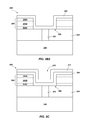
- FIG. 3A through 3D are simplified partial cross-sectional views of a semiconductor structure 300 illustrating embodiments of a method of forming a conductive element for a semiconductor device, such as an electrode 311 of a conductive bridge random access memory (conductive bridge RAM) device.
- a conductive bridge RAM device may include a plurality of memory cells, one of which is shown in FIG. 3A .
- a conductive bridge RAM cell 330 may include a memory material 309 , disposed between a first electrode 308 and a second electrode 311 .
- the memory material 309 may be disposed over a surface of an underlying material or over exposed surfaces of an opening 306 , as will be described in further detail.
- the memory material 309 and the second electrode 311 may overlie a conductive structure 303 that provides an electrical connection between the first and second electrodes 308 and 311 .
- the second electrode 311 may be formed from silver.
- conductive bridge RAM cell 330 While not wishing to be bound by any particular theory, it is believed that operation of the conductive bridge RAM cell 330 occurs due to selective formation and dissolution of a conductive bridge formed by electromigration of silver into the memory material 309 . Thus, it is important to control diffusion of silver ions into the memory material 309 during deposition of the second electrode 311 .
- FIGS. 3 B 1 through 3 D illustrate embodiments of a method of forming the conductive bridge RAM cell 330 shown in FIG. 3A .
- a semiconductor structure 300 may be formed that includes an opening 306 in a dielectric material 304 , the opening 306 overlying a conductive structure 303 in an interlayer dielectric material 305 overlying the first electrode 308 .
- the first electrode 308 may be formed from a conductive material, such as tungsten, platinum, titanium nitride (TiN), or nickel.
- the first electrode 308 may be formed over a substrate (not shown) using conventional deposition process, such as a chemical vapor deposition process or an atomic layer deposition process.
- the semiconductor structure 300 may include the memory material 309 overlying surfaces of the conductive structure 303 and the interlayer dielectric material 305 .
- the interlayer dielectric material 305 may be formed from, for example, silicon nitride, silicon dioxide, or a silicon oxynitride.
- the interlayer dielectric material 305 may be formed over the first electrode 308 using a conventional deposition process, such as a chemical vapor deposition process, an atomic layer deposition process, or a physical vapor deposition process.
- the conductive structure 303 may be formed from a conductive material, such as at least one of titanium nitride, tungsten, tungsten nitride, tantalum, and tantalum nitride.
- the conductive structure 303 may be formed in electrical connection with the first electrode 308 .
- the conductive structure 303 may be formed in the interlayer dielectric material 305 using conventional techniques, the details of which are known in the art and, therefore, are not described in detail herein.
- a conventional damascene process may be used to form the conductive structure 303 in the interlayer dielectric material 305 by forming a trench in the interlayer dielectric material 305 , forming the conductive material over interlayer dielectric material 305 to fill the trench, and performing a chemical mechanical polishing (CMP) process to remove portions of the conductive material overlying the interlayer dielectric material 305 .
- CMP chemical mechanical polishing
- the memory material 309 may be formed from a chalcogenide material, such as germanium selenide or germanium sulfide, or an oxide material, such as a high-k oxide material.
- a chalcogenide material such as germanium selenide or germanium sulfide
- an oxide material such as a high-k oxide material.
- suitable high-k dielectric materials include, but are not limited to, silicon dioxide, tantalum oxide, titanium oxide, nitrogen oxide, zirconium oxide, and hafnium oxide.
- the memory material 309 may be deposited using a conventional deposition process, such as a physical vapor deposition process, a chemical vapor deposition process, or an atomic layer deposition process.
- the dielectric material 304 may be formed from, for example, silicon nitride, tetraethyl orthosilicate (TEOS), silicon dioxide, or a silicon oxynitride.
- the dielectric material 304 may be formed over the interlayer dielectric material 305 and the conductive structure 303 using a conventional deposition process, such as a chemical vapor deposition process, an atomic layer deposition process, or a physical vapor deposition process.
- the dielectric material 304 may be formed as a monolithic structure.
- the dielectric material 304 may be formed as a stacked structure that includes a plurality of materials 304 A. 304 B, 304 C, as shown in broken lines.
- the materials 304 A and 304 C may be formed from silicon nitride and the material 304 B may be formed from tetraethyl orthosilicate.
- the opening 306 may be formed in the dielectric material 304 by removing a portion of the dielectric material 304 using, for example, conventional photolithography techniques (e.g., masking and etching) known in the art of integrated circuit fabrication.
- the portion of the dielectric material 304 removed to form the opening 306 may overlie the conductive structure 303 such that the opening 306 exposes a surface of the conductive structure 303 and, optionally, surfaces of the interlayer dielectric material 305 adjacent the surface of the conductive structure 303 .
- the opening 306 may have a width W 3 of less than about 100 nm and, more particularly, less than about 20 nm.
- the memory material 309 may alternatively be formed over sidewalls of the dielectric material 304 and surfaces of the conductive structure 303 and the interlayer dielectric material 305 after forming the dielectric material 304 and the opening 306 in the dielectric material 304 .
- the memory material 309 may be formed from a chalcogenide material, such as germanium selenide or germanium sulfide, or an oxide material, such as a high-k oxide material, using a conventional deposition process, such as a physical vapor deposition process, a chemical vapor deposition process, or an atomic layer deposition process.
- an annealing process may optionally be performed.
- the annealing process may include exposing the semiconductor structure 300 to a temperature of between about 100° C. and about 500° C. and, more particularly, a temperature of about 200° C.
- a conductive material 312 that includes silver may be formed over the memory material 309 .
- the semiconductor structure 300 is shown with the memory material 309 disposed over surfaces in the opening 306 and over surfaces of the dielectric material 304 .
- the memory material 309 may also be disposed between the interlayer dielectric material 305 and the dielectric material 304 as shown in FIG. 3 B 1 .
- the conductive material 312 may be formed from silver (Ag) or a silver alloy using a conventional sputtering process.
- the conductive material 312 may be substantially conformally deposited over an entire exposed surface of the memory material 309 .
- a thickness of the conductive material 312 may be such that a portion of the opening 306 remains unfilled (i.e., unfilled region 316 ).
- the conductive material 312 may be formed having a thickness of between about 10 nm and about 20 nm.
- a liner material 310 may be formed over surfaces of the conductive material 312 .
- the liner material 310 may be formed from at least one of platinum, tantalum, aluminum (Al), lead (Sb), copper, iridium, titanium, nickel, cobalt, ruthenium, and rhodium.
- the liner material 310 may be formed using a conventional deposition process, such as a chemical vapor deposition process, a physical vapor deposition process, or a sputtering process.
- the liner material 310 may be formed having a thickness of between about 0.5 nm and about 20 nm and, more particularly, between about 1 nm and about 5 nm.
- material i.e., the conductive material 312 and the liner material 310
- material may be pushed or redistributed from upper surfaces of the dielectric material 304 into voids (e.g., the unfilled region 316 of the opening 306 ( FIG. 3C )) by subjecting an exposed surface of the semiconductor structure 300 to a polishing process, as described with respect to FIG. 3D .
- the unfilled region 316 FIGS. 3C and 3D
- an annealing process may then be performed to form an alloy of the conductive material 312 and the liner material 310 .
- the annealing process may be performed to form the alloy.
- the annealing process may be bypassed at this stage.
- the annealing process may include exposing the semiconductor structure 300 to a temperature of between about 100° C. and about 500° C. and, more particularly, about 200° C.
- the conductive material 312 may be formed from silver
- the liner material 310 may be formed from platinum
- a silver-platinum alloy may be formed during the annealing process.
- a majority of the alloy or substantially all of the alloy may be located in a region of the second electrode 311 ( FIG. 3A ) opposite a surface of the memory material 309 such that a region of the second electrode 311 in contact with or adjacent to the memory material 309 substantially includes silver.
- FIGS. 3A through 3D embodiments of methods of forming a silver-containing conductive element (i.e., the second electrode 311 ) are illustrated in the conductive bridge RAM cell 330 .
- such methods may also be used to form other conductive elements in a multitude of semiconductor structures and devices, as would be understood by one of ordinary skill in the art.
- a plurality of trenches was formed in a silicon dioxide material overlying a silicon wafer.
- the trenches of the plurality each had a depth of about 50 nm.
- Silver was deposited over the surface of the silicon wafer using a conventional sputtering process. The sputtering process was performed using a conventional sputter coater. The silver was sputtered over the surface of the silicon wafer for about two minutes, during which time the silver reached a thickness of about 15 nm. Platinum was then formed over the silver using the sputter coater. The platinum was sputtered over the surface of the silicon wafer for about 30 seconds, during which time the platinum reached a thickness of about 6 nm.
- a mechanical polishing process was performed on the silicon wafer having the silver and platinum thereon using deionized water and a conventional polishing pad. No chemical slurry was used during the mechanical polishing process. The surface of the platinum was polished using a pad rotation of about 100 RPM. After the mechanical polishing process, a scanning electron microscope (SEM) was used to observe that the trenches were substantially filled with material (e.g., the silver and the platinum).
- SEM scanning electron microscope
- An annealing process was then performed using a conventional industrial oven.
- the industrial oven was set to 200° C., and the silicon wafer having the silver and platinum thereon was placed therein for about 10 minutes. It was confirmed that the post-annealed silver-platinum alloy was substantially smooth with low resistance.
- the present disclosure includes methods of forming at least one conductive element.
- Such a method may include forming a first conductive material over a structure comprising at least one opening defined by sidewalls of a dielectric material, forming a second conductive material comprising silver over the first conductive material, and annealing the structure to form a material comprising at least a portion of the first conductive material and the second conductive material.
- a method of forming the conductive element may also include forming a conductive material comprising silver over surfaces of a structure comprising at least one opening defined by sidewalls of a dielectric material, forming another conductive material over the conductive material, and performing a polishing process to substantially redistribute at least one of the conductive material and the another conductive material into an unfilled region of the at least one opening.
- the present disclosure includes a method of forming a semiconductor structure.
- the method may include removing a portion of a dielectric material overlying a substrate to form at least one opening therein, forming a first conductive material over the dielectric material and exposed surfaces of the at least one opening, forming a second conductive material comprising silver over the first conductive material, a portion of the at least one opening remaining unfilled, and performing a polishing process to substantially fill the unfilled portion of the at least one opening.
- the present disclosure includes a method of forming a memory cell.
- the method includes forming a first conductive material over surfaces of a structure comprising at least one opening overlying a first electrode, forming a memory material over the first conductive material, forming a second conductive material comprising silver over the memory material, a portion of the at least one opening remaining unfilled, and performing a process to substantially fill the at least one opening with the memory material and the second conductive material.
- the method of forming the memory cell may also include forming a first conductive material comprising silver over surfaces of a memory material exposed by at least one opening overlying a first electrode, forming a second conductive material over the first conductive material, a portion of the at least one opening remaining unfilled, and performing a process to substantially fill the at least one opening with the memory material and the first and second conductive materials.
- the present disclosure includes a semiconductor structure.
- the semiconductor structure may include a conductive structure overlying an electrode, at least one of a chalcogenide material and an oxide material in contact with the conductive structure, and a conductive material overlying the chalcogenide material, the conductive material comprising silver, and at least one region comprising another material.
- the present disclosure includes a memory cell.
- the memory cell includes a memory material overlying an electrode.
- the memory cell also includes a conductive material comprising silver and another material.
- the conductive material overlies the memory material and is disposed in at least one opening.
Abstract
Description
Claims (14)
Priority Applications (4)
| Application Number | Priority Date | Filing Date | Title |
|---|---|---|---|
| US13/961,479 US9520558B2 (en) | 2011-03-17 | 2013-08-07 | Semiconductor structures and memory cells including conductive material and methods of fabrication |
| US15/375,457 US9865812B2 (en) | 2011-03-17 | 2016-12-12 | Methods of forming conductive elements of semiconductor devices and of forming memory cells |
| US15/848,399 US10411186B2 (en) | 2011-03-17 | 2017-12-20 | Semiconductor devices including silver conductive materials |
| US16/538,477 US10862030B2 (en) | 2011-03-17 | 2019-08-12 | Semiconductor devices comprising silver |
Applications Claiming Priority (2)
| Application Number | Priority Date | Filing Date | Title |
|---|---|---|---|
| US13/050,725 US8524599B2 (en) | 2011-03-17 | 2011-03-17 | Methods of forming at least one conductive element and methods of forming a semiconductor structure |
| US13/961,479 US9520558B2 (en) | 2011-03-17 | 2013-08-07 | Semiconductor structures and memory cells including conductive material and methods of fabrication |
Related Parent Applications (1)
| Application Number | Title | Priority Date | Filing Date |
|---|---|---|---|
| US13/050,725 Division US8524599B2 (en) | 2011-03-17 | 2011-03-17 | Methods of forming at least one conductive element and methods of forming a semiconductor structure |
Related Child Applications (1)
| Application Number | Title | Priority Date | Filing Date |
|---|---|---|---|
| US15/375,457 Division US9865812B2 (en) | 2011-03-17 | 2016-12-12 | Methods of forming conductive elements of semiconductor devices and of forming memory cells |
Publications (2)
| Publication Number | Publication Date |
|---|---|
| US20130320291A1 US20130320291A1 (en) | 2013-12-05 |
| US9520558B2 true US9520558B2 (en) | 2016-12-13 |
Family
ID=46827755
Family Applications (5)
| Application Number | Title | Priority Date | Filing Date |
|---|---|---|---|
| US13/050,725 Active US8524599B2 (en) | 2011-03-17 | 2011-03-17 | Methods of forming at least one conductive element and methods of forming a semiconductor structure |
| US13/961,479 Active US9520558B2 (en) | 2011-03-17 | 2013-08-07 | Semiconductor structures and memory cells including conductive material and methods of fabrication |
| US15/375,457 Active US9865812B2 (en) | 2011-03-17 | 2016-12-12 | Methods of forming conductive elements of semiconductor devices and of forming memory cells |
| US15/848,399 Active 2031-06-12 US10411186B2 (en) | 2011-03-17 | 2017-12-20 | Semiconductor devices including silver conductive materials |
| US16/538,477 Active US10862030B2 (en) | 2011-03-17 | 2019-08-12 | Semiconductor devices comprising silver |
Family Applications Before (1)
| Application Number | Title | Priority Date | Filing Date |
|---|---|---|---|
| US13/050,725 Active US8524599B2 (en) | 2011-03-17 | 2011-03-17 | Methods of forming at least one conductive element and methods of forming a semiconductor structure |
Family Applications After (3)
| Application Number | Title | Priority Date | Filing Date |
|---|---|---|---|
| US15/375,457 Active US9865812B2 (en) | 2011-03-17 | 2016-12-12 | Methods of forming conductive elements of semiconductor devices and of forming memory cells |
| US15/848,399 Active 2031-06-12 US10411186B2 (en) | 2011-03-17 | 2017-12-20 | Semiconductor devices including silver conductive materials |
| US16/538,477 Active US10862030B2 (en) | 2011-03-17 | 2019-08-12 | Semiconductor devices comprising silver |
Country Status (8)
| Country | Link |
|---|---|
| US (5) | US8524599B2 (en) |
| EP (1) | EP2686875B1 (en) |
| JP (2) | JP5582326B2 (en) |
| KR (1) | KR101481934B1 (en) |
| CN (2) | CN103503116A (en) |
| SG (1) | SG193501A1 (en) |
| TW (2) | TWI446489B (en) |
| WO (1) | WO2012125610A2 (en) |
Cited By (1)
| Publication number | Priority date | Publication date | Assignee | Title |
|---|---|---|---|---|
| US9865812B2 (en) | 2011-03-17 | 2018-01-09 | Micron Technology, Inc. | Methods of forming conductive elements of semiconductor devices and of forming memory cells |
Families Citing this family (5)
| Publication number | Priority date | Publication date | Assignee | Title |
|---|---|---|---|---|
| US9412790B1 (en) | 2012-12-04 | 2016-08-09 | Crossbar, Inc. | Scalable RRAM device architecture for a non-volatile memory device and method |
| US9947722B2 (en) | 2016-03-16 | 2018-04-17 | Toshiba Memory Corporation | Semiconductor memory device |
| US9991122B2 (en) * | 2016-08-31 | 2018-06-05 | Micron Technology, Inc. | Methods of forming semiconductor device structures including two-dimensional material structures |
| CN107123600A (en) * | 2017-05-19 | 2017-09-01 | 武汉新芯集成电路制造有限公司 | It is a kind of to improve the lithographic method of wafer surface defects |
| US20220277994A1 (en) * | 2021-02-26 | 2022-09-01 | Taiwan Semiconductor Manufacturing Co., Ltd. | Conductive feature of semiconductor device and method of forming same |
Citations (41)
| Publication number | Priority date | Publication date | Assignee | Title |
|---|---|---|---|---|
| US5529954A (en) | 1993-01-05 | 1996-06-25 | Kabushiki Kaisha Toshiba | Method of diffusing a metal through a silver electrode to form a protective film on the surface of the electrode |
| US5719447A (en) | 1993-06-03 | 1998-02-17 | Intel Corporation | Metal alloy interconnections for integrated circuits |
| JP2000040742A (en) | 1998-06-22 | 2000-02-08 | Stmicroelectronics Inc | Silver metalization by damask method |
| US6143655A (en) | 1998-02-25 | 2000-11-07 | Micron Technology, Inc. | Methods and structures for silver interconnections in integrated circuits |
| US6465345B1 (en) | 1999-05-28 | 2002-10-15 | Advanced Micro Devices, Inc. | Prevention of inter-channel current leakage in semiconductors |
| US6511906B1 (en) | 2001-08-30 | 2003-01-28 | Micron Technology, Inc. | Selective CMP scheme |
| US20030041452A1 (en) | 2001-08-30 | 2003-03-06 | Nishant Sinha | Filling plugs through chemical mechanical polish |
| US20030047771A1 (en) | 2001-09-12 | 2003-03-13 | Soon-Yong Kweon | Semiconductor device and method for fabricating the same |
| US20030134436A1 (en) | 2002-01-16 | 2003-07-17 | Yates Donald L. | Method for enhancing electrode surface area in DRAM cell capacitors |
| US20030143838A1 (en) | 2002-01-30 | 2003-07-31 | Michael Kozhukh | Interconnect structures in a semiconductor device and processes of formation |
| US20030203526A1 (en) | 2000-02-01 | 2003-10-30 | Chartered Semiconductor Manufacturing Ltd. | Two layer mirror for LCD-on -silicon products and method of fabrication thereof |
| JP2004040742A (en) | 2002-07-01 | 2004-02-05 | Emuka:Kk | Door-scope image magnification display unit |
| US20040155349A1 (en) | 2003-01-07 | 2004-08-12 | Naofumi Nakamura | Semiconductor device and method of fabricating the same |
| JP2004235620A (en) | 2003-01-07 | 2004-08-19 | Toshiba Corp | Semiconductor device |
| US6936545B1 (en) | 2003-10-01 | 2005-08-30 | Advanced Micro Devices, Inc. | Organic memory cell formation on Ag substrate |
| US20050282378A1 (en) | 2004-06-22 | 2005-12-22 | Akira Fukunaga | Interconnects forming method and interconnects forming apparatus |
| US20060046453A1 (en) | 2004-09-01 | 2006-03-02 | Micron Technology, Inc. | Method for filling electrically different features |
| US20060084271A1 (en) | 2004-10-20 | 2006-04-20 | Yang Andy C | Systems, methods and slurries for chemical mechanical polishing |
| US20060094236A1 (en) | 2004-11-03 | 2006-05-04 | Elkins Patricia C | Electroless plating of metal caps for chalcogenide-based memory devices |
| US7118707B2 (en) | 2004-03-31 | 2006-10-10 | American Bullion Investment Company, Inc. | Silver-platinum alloy and methods of manufacturing same |
| US20060289999A1 (en) | 2005-06-22 | 2006-12-28 | Samsung Electronics Co., Ltd. | Selective copper alloy interconnections in semiconductor devices and methods of forming the same |
| US20070018329A1 (en) | 2005-07-20 | 2007-01-25 | Samsung Electronics Co., Ltd. | Interconnection having dual-level or multi-level capping layer and method of forming the same |
| US7199052B2 (en) | 1999-10-02 | 2007-04-03 | Uri Cohen | Seed layers for metallic interconnects |
| US7229924B2 (en) | 2003-04-15 | 2007-06-12 | Micron Technology, Inc. | Surface barriers for copper and silver interconnects produced by a damascene process |
| JP2007157941A (en) | 2005-12-02 | 2007-06-21 | Sony Corp | Storage element and storage device |
| US20070139987A1 (en) | 2005-12-02 | 2007-06-21 | Sony Corporation | Storage element and storage apparatus |
| US20070145586A1 (en) | 2005-12-27 | 2007-06-28 | Kabushiki Kaisha Kobe Seiko Sho(Kobe Steel, Ltd.) | Metal thin film for interconnection of semiconductor device, interconnection for semiconductor device, and their fabrication method |
| US20080036508A1 (en) | 2004-12-27 | 2008-02-14 | Nec Corporation | Switching Element, Switching Element Drive Method and Fabrication Method, Reconfigurable Logic Integrated Circuit, and Memory Element |
| US7332401B2 (en) | 2001-11-19 | 2008-02-19 | Micron Technology, Ing. | Method of fabricating an electrode structure for use in an integrated circuit |
| US20080128912A1 (en) | 2006-11-30 | 2008-06-05 | Christof Streck | Semiconductor structure and method of forming the same |
| US7423282B2 (en) | 2006-07-06 | 2008-09-09 | Infineon Technologies Ag | Memory structure and method of manufacture |
| US20080253165A1 (en) | 2007-04-10 | 2008-10-16 | Philippe Blanchard | Method of Manufacturing a Memory Device, Memory Device, Cell, Integrated Circuit, Memory Module, and Computing System |
| US20090239398A1 (en) | 2008-03-20 | 2009-09-24 | Interplex Nas, Inc. | Press fit (compliant) terminal and other connectors with tin-silver compound |
| US20100003814A1 (en) | 2002-12-30 | 2010-01-07 | Samsung Electronics Co., Ltd. | Interconnections Having Double Capping Layer and Method for Forming the Same |
| US20100078820A1 (en) | 2008-09-30 | 2010-04-01 | Nec Electronics Corporation | Semiconductor device and method of manufacturing the same |
| US7694871B2 (en) | 2003-10-31 | 2010-04-13 | International Business Machines Corporation | Self-encapsulated silver alloys for interconnects |
| US7718537B2 (en) | 2004-09-30 | 2010-05-18 | Qimonda Ag | Method for manufacturing a CBRAM semiconductor memory |
| US20100163829A1 (en) | 2008-12-30 | 2010-07-01 | Industrial Technology Research Institute | Conductive bridging random access memory device and method of manufacturing the same |
| US20100193758A1 (en) | 2009-01-30 | 2010-08-05 | Seagate Technology Llc | Programmable metallization memory cell with planarized silver electrode |
| US20110115096A1 (en) | 2002-11-23 | 2011-05-19 | Infineon Technologies Ag | Electrodepositing a metal in integrated circuit applications |
| US20120235106A1 (en) | 2011-03-17 | 2012-09-20 | Micron Technology, Inc. | Methods of forming at least one conductive element, methods of forming a semiconductor structure, methods of forming a memory cell and related semiconductor structures |
Family Cites Families (25)
| Publication number | Priority date | Publication date | Assignee | Title |
|---|---|---|---|---|
| JP2002237493A (en) * | 1994-02-21 | 2002-08-23 | Toshiba Corp | Manufacturing method of semiconductor device |
| DE19640273C1 (en) * | 1996-09-30 | 1998-03-12 | Siemens Ag | Method for manufacturing barrier-free semiconductor memory devices |
| US6165864A (en) * | 1998-07-28 | 2000-12-26 | Siemens Aktiengesellschaft | Tapered electrode for stacked capacitors |
| US7253076B1 (en) * | 2000-06-08 | 2007-08-07 | Micron Technologies, Inc. | Methods for forming and integrated circuit structures containing ruthenium and tungsten containing layers |
| US6482736B1 (en) * | 2000-06-08 | 2002-11-19 | Micron Technology, Inc. | Methods for forming and integrated circuit structures containing enhanced-surface-area conductive layers |
| JP2002261099A (en) * | 2001-02-27 | 2002-09-13 | Tokyo Electron Ltd | Semiconductor device and wiring formation method thereof |
| US6696360B2 (en) * | 2001-03-15 | 2004-02-24 | Micron Technology, Inc. | Barrier-metal-free copper damascene technology using atomic hydrogen enhanced reflow |
| US6586761B2 (en) * | 2001-09-07 | 2003-07-01 | Intel Corporation | Phase change material memory device |
| JP2003289134A (en) * | 2002-03-28 | 2003-10-10 | Matsushita Electric Ind Co Ltd | Semiconductor device and manufacturing method therefor |
| WO2004017438A1 (en) * | 2002-08-14 | 2004-02-26 | Intel Corporation | Adhesive material for programmable device |
| DE10254815A1 (en) * | 2002-11-23 | 2004-06-09 | Infineon Technologies Ag | Process for the galvanic application of a metal, in particular copper, use of this process and integrated circuit arrangement |
| KR100725690B1 (en) * | 2003-07-08 | 2007-06-07 | 마츠시타 덴끼 산교 가부시키가이샤 | Semiconductor device and method for fabricating the same |
| JP4571836B2 (en) * | 2004-07-23 | 2010-10-27 | ルネサスエレクトロニクス株式会社 | Semiconductor device and manufacturing method thereof |
| CN1738026A (en) * | 2004-08-20 | 2006-02-22 | 松下电器产业株式会社 | Dielectric memory device and method for fabricating the same |
| CN100449709C (en) * | 2005-02-14 | 2009-01-07 | 东京毅力科创株式会社 | Method of processing and cleaning substrate, and method of and program for manufacturing electronic device |
| CN1929160A (en) * | 2005-09-07 | 2007-03-14 | 财团法人工业技术研究院 | Method and structure for improving property of phase-changing storage |
| CN100423283C (en) * | 2006-07-20 | 2008-10-01 | 复旦大学 | Novel channel structure phase change storage |
| CN100511685C (en) * | 2006-12-22 | 2009-07-08 | 上海宏力半导体制造有限公司 | Capacitor apparatus and method of manufacture |
| KR20080064605A (en) * | 2007-01-05 | 2008-07-09 | 삼성전자주식회사 | Phase change memory device and method of manufacturing for the same |
| US20080265239A1 (en) * | 2007-04-26 | 2008-10-30 | Jan Boris Philipp | Integrated circuit including spacer material layer |
| CN101312230B (en) * | 2007-05-25 | 2010-10-13 | 财团法人工业技术研究院 | Phase change storage apparatus and method of manufacture |
| KR20090013419A (en) * | 2007-08-01 | 2009-02-05 | 삼성전자주식회사 | Phase change memory devices and methods of forming the same |
| US8753933B2 (en) * | 2008-11-19 | 2014-06-17 | Micron Technology, Inc. | Methods for forming a conductive material, methods for selectively forming a conductive material, methods for forming platinum, and methods for forming conductive structures |
| KR101279966B1 (en) * | 2008-12-29 | 2013-07-05 | 제일모직주식회사 | CMP slurry composition for polishing metal wiring and polishing method using the same |
| JP2010165803A (en) * | 2009-01-14 | 2010-07-29 | Toshiba Corp | Method of manufacturing semiconductor memory device, and semiconductor memory device |
-
2011
- 2011-03-17 US US13/050,725 patent/US8524599B2/en active Active
-
2012
- 2012-03-13 SG SG2013069836A patent/SG193501A1/en unknown
- 2012-03-13 KR KR1020137025995A patent/KR101481934B1/en active IP Right Grant
- 2012-03-13 WO PCT/US2012/028878 patent/WO2012125610A2/en active Application Filing
- 2012-03-13 CN CN201280018861.1A patent/CN103503116A/en active Pending
- 2012-03-13 EP EP12757934.0A patent/EP2686875B1/en active Active
- 2012-03-13 JP JP2013558103A patent/JP5582326B2/en active Active
- 2012-03-13 CN CN201710243903.6A patent/CN107275282A/en active Pending
- 2012-03-16 TW TW101109223A patent/TWI446489B/en active
- 2012-03-16 TW TW103120618A patent/TWI590378B/en active
-
2013
- 2013-08-07 US US13/961,479 patent/US9520558B2/en active Active
-
2014
- 2014-07-01 JP JP2014135499A patent/JP5805275B2/en active Active
-
2016
- 2016-12-12 US US15/375,457 patent/US9865812B2/en active Active
-
2017
- 2017-12-20 US US15/848,399 patent/US10411186B2/en active Active
-
2019
- 2019-08-12 US US16/538,477 patent/US10862030B2/en active Active
Patent Citations (53)
| Publication number | Priority date | Publication date | Assignee | Title |
|---|---|---|---|---|
| US5529954A (en) | 1993-01-05 | 1996-06-25 | Kabushiki Kaisha Toshiba | Method of diffusing a metal through a silver electrode to form a protective film on the surface of the electrode |
| US5719447A (en) | 1993-06-03 | 1998-02-17 | Intel Corporation | Metal alloy interconnections for integrated circuits |
| US6143655A (en) | 1998-02-25 | 2000-11-07 | Micron Technology, Inc. | Methods and structures for silver interconnections in integrated circuits |
| JP2000040742A (en) | 1998-06-22 | 2000-02-08 | Stmicroelectronics Inc | Silver metalization by damask method |
| US6100194A (en) | 1998-06-22 | 2000-08-08 | Stmicroelectronics, Inc. | Silver metallization by damascene method |
| US6465345B1 (en) | 1999-05-28 | 2002-10-15 | Advanced Micro Devices, Inc. | Prevention of inter-channel current leakage in semiconductors |
| US7199052B2 (en) | 1999-10-02 | 2007-04-03 | Uri Cohen | Seed layers for metallic interconnects |
| US20030203526A1 (en) | 2000-02-01 | 2003-10-30 | Chartered Semiconductor Manufacturing Ltd. | Two layer mirror for LCD-on -silicon products and method of fabrication thereof |
| US6969301B2 (en) | 2001-08-30 | 2005-11-29 | Micron Technology, Inc. | Filling plugs through chemical mechanical polish |
| US6757971B2 (en) | 2001-08-30 | 2004-07-06 | Micron Technology, Inc. | Filling plugs through chemical mechanical polish |
| US20030041452A1 (en) | 2001-08-30 | 2003-03-06 | Nishant Sinha | Filling plugs through chemical mechanical polish |
| US6946392B2 (en) | 2001-08-30 | 2005-09-20 | Micron Technology, Inc. | Filling plugs through chemical mechanical polish |
| US6511906B1 (en) | 2001-08-30 | 2003-01-28 | Micron Technology, Inc. | Selective CMP scheme |
| US20030047771A1 (en) | 2001-09-12 | 2003-03-13 | Soon-Yong Kweon | Semiconductor device and method for fabricating the same |
| JP2003133534A (en) | 2001-09-12 | 2003-05-09 | Hynix Semiconductor Inc | Semiconductor element and manufacturing method therefor |
| US7332401B2 (en) | 2001-11-19 | 2008-02-19 | Micron Technology, Ing. | Method of fabricating an electrode structure for use in an integrated circuit |
| TW591705B (en) | 2002-01-16 | 2004-06-11 | Micron Technology Inc | Method for enhancing electrode surface area in DRAM cell capacitors |
| US20030134436A1 (en) | 2002-01-16 | 2003-07-17 | Yates Donald L. | Method for enhancing electrode surface area in DRAM cell capacitors |
| US20040038523A1 (en) | 2002-01-30 | 2004-02-26 | Michael Kozhukh | Interconnect structures in a semiconductor device and processes of formation |
| US7033930B2 (en) | 2002-01-30 | 2006-04-25 | Intel Corporation | Interconnect structures in a semiconductor device and processes of formation |
| US20030143838A1 (en) | 2002-01-30 | 2003-07-31 | Michael Kozhukh | Interconnect structures in a semiconductor device and processes of formation |
| JP2004040742A (en) | 2002-07-01 | 2004-02-05 | Emuka:Kk | Door-scope image magnification display unit |
| US20110115096A1 (en) | 2002-11-23 | 2011-05-19 | Infineon Technologies Ag | Electrodepositing a metal in integrated circuit applications |
| US20100003814A1 (en) | 2002-12-30 | 2010-01-07 | Samsung Electronics Co., Ltd. | Interconnections Having Double Capping Layer and Method for Forming the Same |
| JP2004235620A (en) | 2003-01-07 | 2004-08-19 | Toshiba Corp | Semiconductor device |
| US20040155349A1 (en) | 2003-01-07 | 2004-08-12 | Naofumi Nakamura | Semiconductor device and method of fabricating the same |
| US7229924B2 (en) | 2003-04-15 | 2007-06-12 | Micron Technology, Inc. | Surface barriers for copper and silver interconnects produced by a damascene process |
| US6936545B1 (en) | 2003-10-01 | 2005-08-30 | Advanced Micro Devices, Inc. | Organic memory cell formation on Ag substrate |
| US7694871B2 (en) | 2003-10-31 | 2010-04-13 | International Business Machines Corporation | Self-encapsulated silver alloys for interconnects |
| US7118707B2 (en) | 2004-03-31 | 2006-10-10 | American Bullion Investment Company, Inc. | Silver-platinum alloy and methods of manufacturing same |
| US20050282378A1 (en) | 2004-06-22 | 2005-12-22 | Akira Fukunaga | Interconnects forming method and interconnects forming apparatus |
| US20060046453A1 (en) | 2004-09-01 | 2006-03-02 | Micron Technology, Inc. | Method for filling electrically different features |
| US7718537B2 (en) | 2004-09-30 | 2010-05-18 | Qimonda Ag | Method for manufacturing a CBRAM semiconductor memory |
| CN100533674C (en) | 2004-10-20 | 2009-08-26 | 安集微电子(上海)有限公司 | Method and abrasive slurry for chemical mechanical polishing, and semiconductor device and its manufacture method |
| US20060084271A1 (en) | 2004-10-20 | 2006-04-20 | Yang Andy C | Systems, methods and slurries for chemical mechanical polishing |
| US20060094236A1 (en) | 2004-11-03 | 2006-05-04 | Elkins Patricia C | Electroless plating of metal caps for chalcogenide-based memory devices |
| US20080036508A1 (en) | 2004-12-27 | 2008-02-14 | Nec Corporation | Switching Element, Switching Element Drive Method and Fabrication Method, Reconfigurable Logic Integrated Circuit, and Memory Element |
| US20060289999A1 (en) | 2005-06-22 | 2006-12-28 | Samsung Electronics Co., Ltd. | Selective copper alloy interconnections in semiconductor devices and methods of forming the same |
| US20070018329A1 (en) | 2005-07-20 | 2007-01-25 | Samsung Electronics Co., Ltd. | Interconnection having dual-level or multi-level capping layer and method of forming the same |
| JP2007027769A (en) | 2005-07-20 | 2007-02-01 | Samsung Electronics Co Ltd | Interconnect line of semiconductor device having double capping film and its forming method |
| JP2007157942A (en) | 2005-12-02 | 2007-06-21 | Sony Corp | Storage element and storage device |
| US20070139987A1 (en) | 2005-12-02 | 2007-06-21 | Sony Corporation | Storage element and storage apparatus |
| JP2007157941A (en) | 2005-12-02 | 2007-06-21 | Sony Corp | Storage element and storage device |
| JP2007180173A (en) | 2005-12-27 | 2007-07-12 | Kobe Steel Ltd | Wiring of semiconductor device, metal thin film therefor, and these manufacturing methods |
| US20070145586A1 (en) | 2005-12-27 | 2007-06-28 | Kabushiki Kaisha Kobe Seiko Sho(Kobe Steel, Ltd.) | Metal thin film for interconnection of semiconductor device, interconnection for semiconductor device, and their fabrication method |
| US7423282B2 (en) | 2006-07-06 | 2008-09-09 | Infineon Technologies Ag | Memory structure and method of manufacture |
| US20080128912A1 (en) | 2006-11-30 | 2008-06-05 | Christof Streck | Semiconductor structure and method of forming the same |
| US20080253165A1 (en) | 2007-04-10 | 2008-10-16 | Philippe Blanchard | Method of Manufacturing a Memory Device, Memory Device, Cell, Integrated Circuit, Memory Module, and Computing System |
| US20090239398A1 (en) | 2008-03-20 | 2009-09-24 | Interplex Nas, Inc. | Press fit (compliant) terminal and other connectors with tin-silver compound |
| US20100078820A1 (en) | 2008-09-30 | 2010-04-01 | Nec Electronics Corporation | Semiconductor device and method of manufacturing the same |
| US20100163829A1 (en) | 2008-12-30 | 2010-07-01 | Industrial Technology Research Institute | Conductive bridging random access memory device and method of manufacturing the same |
| US20100193758A1 (en) | 2009-01-30 | 2010-08-05 | Seagate Technology Llc | Programmable metallization memory cell with planarized silver electrode |
| US20120235106A1 (en) | 2011-03-17 | 2012-09-20 | Micron Technology, Inc. | Methods of forming at least one conductive element, methods of forming a semiconductor structure, methods of forming a memory cell and related semiconductor structures |
Non-Patent Citations (10)
| Title |
|---|
| European Office Action for European Application No. 12757934.0, (dated Jun. 12, 2015), 4 pages. |
| Gao et al., "Thermal Stability of Titanium Nitride Diffusion Barrier Films for Advanced Silver Interconnects," Microelectronic Engineering, vol. 76, (2004), pp. 76-81. |
| International Preliminary Report on Patentability for PCT Application No. PCT/US2012/028878, (dated Sep. 17, 2013), 6 pages. |
| Japanese Office Action for Japanese Application No. 2014-135499, (dated Apr. 21, 2015), 5 pages (with annotation indicating translated sections). |
| PCT International Search Report and Written Opinion for PCT Application No. PCT/US2012/028878, mailed Oct. 16, 2012, 8 pages. |
| Search Report for Taiwan Application No. 101109223, (dated Jan. 14, 2014), 1 page. |
| Search Report of the State Intellectual Property Office of China, Chinese Application No. 201280018861.1, (dated Nov. 17, 2014), 2 pages. |
| Supplementary European Search Report and Search Opinion, Application No. EP 12757934.0, Aug. 4, 2014, nine (9) pages. |
| Taiwan Office Action and Search Report for Taiwan Application No. 103120618 dated Dec. 16, 2015, ten (10) pages. |
| Ushiku et al., "Planarized Silver Interconnect Technology with a Ti Self-Passivation Technique for Deep Sub-Micron ULSIs," VLSI Technology Digest of Technical Papers, (1993), pp. 121-122. |
Cited By (3)
| Publication number | Priority date | Publication date | Assignee | Title |
|---|---|---|---|---|
| US9865812B2 (en) | 2011-03-17 | 2018-01-09 | Micron Technology, Inc. | Methods of forming conductive elements of semiconductor devices and of forming memory cells |
| US10411186B2 (en) | 2011-03-17 | 2019-09-10 | Micron Technology, Inc. | Semiconductor devices including silver conductive materials |
| US10862030B2 (en) | 2011-03-17 | 2020-12-08 | Micron Technology, Inc. | Semiconductor devices comprising silver |
Also Published As
| Publication number | Publication date |
|---|---|
| EP2686875A4 (en) | 2014-09-03 |
| TW201244005A (en) | 2012-11-01 |
| SG193501A1 (en) | 2013-10-30 |
| JP2014508422A (en) | 2014-04-03 |
| US9865812B2 (en) | 2018-01-09 |
| CN103503116A (en) | 2014-01-08 |
| US20180114901A1 (en) | 2018-04-26 |
| KR101481934B1 (en) | 2015-01-12 |
| TWI590378B (en) | 2017-07-01 |
| US20130320291A1 (en) | 2013-12-05 |
| TW201438148A (en) | 2014-10-01 |
| US8524599B2 (en) | 2013-09-03 |
| WO2012125610A3 (en) | 2012-12-06 |
| EP2686875A2 (en) | 2014-01-22 |
| KR20130133025A (en) | 2013-12-05 |
| US10411186B2 (en) | 2019-09-10 |
| US10862030B2 (en) | 2020-12-08 |
| JP5805275B2 (en) | 2015-11-04 |
| TWI446489B (en) | 2014-07-21 |
| US20190363253A1 (en) | 2019-11-28 |
| US20120235106A1 (en) | 2012-09-20 |
| JP5582326B2 (en) | 2014-09-03 |
| CN107275282A (en) | 2017-10-20 |
| US20170092855A1 (en) | 2017-03-30 |
| JP2014222760A (en) | 2014-11-27 |
| EP2686875B1 (en) | 2016-09-28 |
| WO2012125610A2 (en) | 2012-09-20 |
Similar Documents
| Publication | Publication Date | Title |
|---|---|---|
| US10862030B2 (en) | Semiconductor devices comprising silver | |
| US5614437A (en) | Method for fabricating reliable metallization with Ta-Si-N barrier for semiconductors | |
| JP4685352B2 (en) | An integrated circuit manufacturing method, an implantation method after copper seed deposition, a barrier / seed interface layer formation method, and a via formation in an integrated circuit. | |
| US6943111B2 (en) | Barrier free copper interconnect by multi-layer copper seed | |
| TWI298510B (en) | Semiconductor device and method for manufacturing same | |
| US6566258B1 (en) | Bi-layer etch stop for inter-level via | |
| TW201241925A (en) | Cobalt metal barrier layers | |
| JPH08148560A (en) | Wiring structure of semiconductor device and its manufacture | |
| US20090166867A1 (en) | Metal interconnect structures for semiconductor devices | |
| US11062943B2 (en) | Top via interconnects with wrap around liner | |
| US6849541B1 (en) | Method of fabricating a dual damascene copper wire | |
| US20070218686A1 (en) | Alluminum base conductor for via fill interconnect | |
| US6150268A (en) | Barrier materials for metal interconnect | |
| WO2003046979A2 (en) | Method of using ternary copper alloy to obtain a low resistance and large grain size interconnect | |
| JP2006165378A (en) | Method for manufacturing semiconductor device | |
| US7169706B2 (en) | Method of using an adhesion precursor layer for chemical vapor deposition (CVD) copper deposition | |
| CN111430295A (en) | Interconnection structure, manufacturing method thereof and semiconductor device | |
| WO2023116329A1 (en) | Hybrid metal interconnects | |
| JPH11330001A (en) | Semiconductor device and manufacturing method therefor |
Legal Events
| Date | Code | Title | Description |
|---|---|---|---|
| FEPP | Fee payment procedure |
Free format text: PAYOR NUMBER ASSIGNED (ORIGINAL EVENT CODE: ASPN); ENTITY STATUS OF PATENT OWNER: LARGE ENTITY |
|
| AS | Assignment |
Owner name: U.S. BANK NATIONAL ASSOCIATION, AS COLLATERAL AGENT, CALIFORNIA Free format text: SECURITY INTEREST;ASSIGNOR:MICRON TECHNOLOGY, INC.;REEL/FRAME:038669/0001 Effective date: 20160426 Owner name: U.S. BANK NATIONAL ASSOCIATION, AS COLLATERAL AGEN Free format text: SECURITY INTEREST;ASSIGNOR:MICRON TECHNOLOGY, INC.;REEL/FRAME:038669/0001 Effective date: 20160426 |
|
| AS | Assignment |
Owner name: MORGAN STANLEY SENIOR FUNDING, INC., AS COLLATERAL AGENT, MARYLAND Free format text: PATENT SECURITY AGREEMENT;ASSIGNOR:MICRON TECHNOLOGY, INC.;REEL/FRAME:038954/0001 Effective date: 20160426 Owner name: MORGAN STANLEY SENIOR FUNDING, INC., AS COLLATERAL Free format text: PATENT SECURITY AGREEMENT;ASSIGNOR:MICRON TECHNOLOGY, INC.;REEL/FRAME:038954/0001 Effective date: 20160426 |
|
| STCF | Information on status: patent grant |
Free format text: PATENTED CASE |
|
| CC | Certificate of correction | ||
| AS | Assignment |
Owner name: U.S. BANK NATIONAL ASSOCIATION, AS COLLATERAL AGENT, CALIFORNIA Free format text: CORRECTIVE ASSIGNMENT TO CORRECT THE REPLACE ERRONEOUSLY FILED PATENT #7358718 WITH THE CORRECT PATENT #7358178 PREVIOUSLY RECORDED ON REEL 038669 FRAME 0001. ASSIGNOR(S) HEREBY CONFIRMS THE SECURITY INTEREST;ASSIGNOR:MICRON TECHNOLOGY, INC.;REEL/FRAME:043079/0001 Effective date: 20160426 Owner name: U.S. BANK NATIONAL ASSOCIATION, AS COLLATERAL AGEN Free format text: CORRECTIVE ASSIGNMENT TO CORRECT THE REPLACE ERRONEOUSLY FILED PATENT #7358718 WITH THE CORRECT PATENT #7358178 PREVIOUSLY RECORDED ON REEL 038669 FRAME 0001. ASSIGNOR(S) HEREBY CONFIRMS THE SECURITY INTEREST;ASSIGNOR:MICRON TECHNOLOGY, INC.;REEL/FRAME:043079/0001 Effective date: 20160426 |
|
| AS | Assignment |
Owner name: JPMORGAN CHASE BANK, N.A., AS COLLATERAL AGENT, ILLINOIS Free format text: SECURITY INTEREST;ASSIGNORS:MICRON TECHNOLOGY, INC.;MICRON SEMICONDUCTOR PRODUCTS, INC.;REEL/FRAME:047540/0001 Effective date: 20180703 Owner name: JPMORGAN CHASE BANK, N.A., AS COLLATERAL AGENT, IL Free format text: SECURITY INTEREST;ASSIGNORS:MICRON TECHNOLOGY, INC.;MICRON SEMICONDUCTOR PRODUCTS, INC.;REEL/FRAME:047540/0001 Effective date: 20180703 |
|
| AS | Assignment |
Owner name: MICRON TECHNOLOGY, INC., IDAHO Free format text: RELEASE BY SECURED PARTY;ASSIGNOR:U.S. BANK NATIONAL ASSOCIATION, AS COLLATERAL AGENT;REEL/FRAME:047243/0001 Effective date: 20180629 |
|
| AS | Assignment |
Owner name: MICRON TECHNOLOGY, INC., IDAHO Free format text: RELEASE BY SECURED PARTY;ASSIGNOR:MORGAN STANLEY SENIOR FUNDING, INC., AS COLLATERAL AGENT;REEL/FRAME:050937/0001 Effective date: 20190731 |
|
| AS | Assignment |
Owner name: MICRON SEMICONDUCTOR PRODUCTS, INC., IDAHO Free format text: RELEASE BY SECURED PARTY;ASSIGNOR:JPMORGAN CHASE BANK, N.A., AS COLLATERAL AGENT;REEL/FRAME:051028/0001 Effective date: 20190731 Owner name: MICRON TECHNOLOGY, INC., IDAHO Free format text: RELEASE BY SECURED PARTY;ASSIGNOR:JPMORGAN CHASE BANK, N.A., AS COLLATERAL AGENT;REEL/FRAME:051028/0001 Effective date: 20190731 |
|
| MAFP | Maintenance fee payment |
Free format text: PAYMENT OF MAINTENANCE FEE, 4TH YEAR, LARGE ENTITY (ORIGINAL EVENT CODE: M1551); ENTITY STATUS OF PATENT OWNER: LARGE ENTITY Year of fee payment: 4 |