US9531164B2 - Optical device structure using GaN substrates for laser applications - Google Patents
Optical device structure using GaN substrates for laser applications Download PDFInfo
- Publication number
- US9531164B2 US9531164B2 US12/759,273 US75927310A US9531164B2 US 9531164 B2 US9531164 B2 US 9531164B2 US 75927310 A US75927310 A US 75927310A US 9531164 B2 US9531164 B2 US 9531164B2
- Authority
- US
- United States
- Prior art keywords
- cleaved
- laser
- facet
- region
- face facet
- Prior art date
- Legal status (The legal status is an assumption and is not a legal conclusion. Google has not performed a legal analysis and makes no representation as to the accuracy of the status listed.)
- Active
Links
Images


Classifications
-
- H—ELECTRICITY
- H01—ELECTRIC ELEMENTS
- H01S—DEVICES USING THE PROCESS OF LIGHT AMPLIFICATION BY STIMULATED EMISSION OF RADIATION [LASER] TO AMPLIFY OR GENERATE LIGHT; DEVICES USING STIMULATED EMISSION OF ELECTROMAGNETIC RADIATION IN WAVE RANGES OTHER THAN OPTICAL
- H01S5/00—Semiconductor lasers
- H01S5/20—Structure or shape of the semiconductor body to guide the optical wave ; Confining structures perpendicular to the optical axis, e.g. index or gain guiding, stripe geometry, broad area lasers, gain tailoring, transverse or lateral reflectors, special cladding structures, MQW barrier reflection layers
- H01S5/22—Structure or shape of the semiconductor body to guide the optical wave ; Confining structures perpendicular to the optical axis, e.g. index or gain guiding, stripe geometry, broad area lasers, gain tailoring, transverse or lateral reflectors, special cladding structures, MQW barrier reflection layers having a ridge or stripe structure
- H01S5/2201—Structure or shape of the semiconductor body to guide the optical wave ; Confining structures perpendicular to the optical axis, e.g. index or gain guiding, stripe geometry, broad area lasers, gain tailoring, transverse or lateral reflectors, special cladding structures, MQW barrier reflection layers having a ridge or stripe structure in a specific crystallographic orientation
-
- H—ELECTRICITY
- H01—ELECTRIC ELEMENTS
- H01L—SEMICONDUCTOR DEVICES NOT COVERED BY CLASS H10
- H01L21/00—Processes or apparatus adapted for the manufacture or treatment of semiconductor or solid state devices or of parts thereof
- H01L21/02—Manufacture or treatment of semiconductor devices or of parts thereof
- H01L21/02104—Forming layers
- H01L21/02365—Forming inorganic semiconducting materials on a substrate
- H01L21/02367—Substrates
- H01L21/0237—Materials
- H01L21/02387—Group 13/15 materials
- H01L21/02389—Nitrides
-
- H—ELECTRICITY
- H01—ELECTRIC ELEMENTS
- H01L—SEMICONDUCTOR DEVICES NOT COVERED BY CLASS H10
- H01L21/00—Processes or apparatus adapted for the manufacture or treatment of semiconductor or solid state devices or of parts thereof
- H01L21/02—Manufacture or treatment of semiconductor devices or of parts thereof
- H01L21/02104—Forming layers
- H01L21/02365—Forming inorganic semiconducting materials on a substrate
- H01L21/02367—Substrates
- H01L21/02433—Crystal orientation
-
- H—ELECTRICITY
- H01—ELECTRIC ELEMENTS
- H01L—SEMICONDUCTOR DEVICES NOT COVERED BY CLASS H10
- H01L21/00—Processes or apparatus adapted for the manufacture or treatment of semiconductor or solid state devices or of parts thereof
- H01L21/02—Manufacture or treatment of semiconductor devices or of parts thereof
- H01L21/02104—Forming layers
- H01L21/02365—Forming inorganic semiconducting materials on a substrate
- H01L21/02518—Deposited layers
- H01L21/02521—Materials
- H01L21/02538—Group 13/15 materials
- H01L21/0254—Nitrides
-
- H—ELECTRICITY
- H01—ELECTRIC ELEMENTS
- H01S—DEVICES USING THE PROCESS OF LIGHT AMPLIFICATION BY STIMULATED EMISSION OF RADIATION [LASER] TO AMPLIFY OR GENERATE LIGHT; DEVICES USING STIMULATED EMISSION OF ELECTROMAGNETIC RADIATION IN WAVE RANGES OTHER THAN OPTICAL
- H01S5/00—Semiconductor lasers
- H01S5/02—Structural details or components not essential to laser action
- H01S5/0201—Separation of the wafer into individual elements, e.g. by dicing, cleaving, etching or directly during growth
- H01S5/0202—Cleaving
-
- H—ELECTRICITY
- H01—ELECTRIC ELEMENTS
- H01S—DEVICES USING THE PROCESS OF LIGHT AMPLIFICATION BY STIMULATED EMISSION OF RADIATION [LASER] TO AMPLIFY OR GENERATE LIGHT; DEVICES USING STIMULATED EMISSION OF ELECTROMAGNETIC RADIATION IN WAVE RANGES OTHER THAN OPTICAL
- H01S5/00—Semiconductor lasers
- H01S5/02—Structural details or components not essential to laser action
- H01S5/028—Coatings ; Treatment of the laser facets, e.g. etching, passivation layers or reflecting layers
- H01S5/0287—Facet reflectivity
-
- H—ELECTRICITY
- H01—ELECTRIC ELEMENTS
- H01S—DEVICES USING THE PROCESS OF LIGHT AMPLIFICATION BY STIMULATED EMISSION OF RADIATION [LASER] TO AMPLIFY OR GENERATE LIGHT; DEVICES USING STIMULATED EMISSION OF ELECTROMAGNETIC RADIATION IN WAVE RANGES OTHER THAN OPTICAL
- H01S5/00—Semiconductor lasers
- H01S5/20—Structure or shape of the semiconductor body to guide the optical wave ; Confining structures perpendicular to the optical axis, e.g. index or gain guiding, stripe geometry, broad area lasers, gain tailoring, transverse or lateral reflectors, special cladding structures, MQW barrier reflection layers
- H01S5/2004—Confining in the direction perpendicular to the layer structure
- H01S5/2009—Confining in the direction perpendicular to the layer structure by using electron barrier layers
-
- H—ELECTRICITY
- H01—ELECTRIC ELEMENTS
- H01S—DEVICES USING THE PROCESS OF LIGHT AMPLIFICATION BY STIMULATED EMISSION OF RADIATION [LASER] TO AMPLIFY OR GENERATE LIGHT; DEVICES USING STIMULATED EMISSION OF ELECTROMAGNETIC RADIATION IN WAVE RANGES OTHER THAN OPTICAL
- H01S5/00—Semiconductor lasers
- H01S5/30—Structure or shape of the active region; Materials used for the active region
- H01S5/32—Structure or shape of the active region; Materials used for the active region comprising PN junctions, e.g. hetero- or double- heterostructures
- H01S5/3202—Structure or shape of the active region; Materials used for the active region comprising PN junctions, e.g. hetero- or double- heterostructures grown on specifically orientated substrates, or using orientation dependent growth
- H01S5/32025—Structure or shape of the active region; Materials used for the active region comprising PN junctions, e.g. hetero- or double- heterostructures grown on specifically orientated substrates, or using orientation dependent growth non-polar orientation
-
- H—ELECTRICITY
- H01—ELECTRIC ELEMENTS
- H01S—DEVICES USING THE PROCESS OF LIGHT AMPLIFICATION BY STIMULATED EMISSION OF RADIATION [LASER] TO AMPLIFY OR GENERATE LIGHT; DEVICES USING STIMULATED EMISSION OF ELECTROMAGNETIC RADIATION IN WAVE RANGES OTHER THAN OPTICAL
- H01S5/00—Semiconductor lasers
- H01S5/30—Structure or shape of the active region; Materials used for the active region
- H01S5/32—Structure or shape of the active region; Materials used for the active region comprising PN junctions, e.g. hetero- or double- heterostructures
- H01S5/323—Structure or shape of the active region; Materials used for the active region comprising PN junctions, e.g. hetero- or double- heterostructures in AIIIBV compounds, e.g. AlGaAs-laser, InP-based laser
- H01S5/32308—Structure or shape of the active region; Materials used for the active region comprising PN junctions, e.g. hetero- or double- heterostructures in AIIIBV compounds, e.g. AlGaAs-laser, InP-based laser emitting light at a wavelength less than 900 nm
- H01S5/32341—Structure or shape of the active region; Materials used for the active region comprising PN junctions, e.g. hetero- or double- heterostructures in AIIIBV compounds, e.g. AlGaAs-laser, InP-based laser emitting light at a wavelength less than 900 nm blue laser based on GaN or GaP
Definitions
- This invention is directed to optical devices and related methods. More particularly, the present invention provides a method and device for emitting electromagnetic radiation using nonpolar gallium containing substrates such as GaN, MN, InN, InGaN, AlGaN, and AlInGaN, and others.
- the invention can be applied to optical devices, lasers, light emitting diodes, solar cells, photoelectrochemical water splitting and hydrogen generation, photodetectors, integrated circuits, and transistors, among other devices.
- the conventional light bulb commonly called the “Edison bulb,” has been used for over one hundred years for a variety of applications including lighting and displays.
- the conventional light bulb uses a tungsten filament enclosed in a glass bulb sealed in a base, which is screwed into a socket. The socket is coupled to an AC power or DC power source.
- the conventional light bulb can be found commonly in houses, buildings, and outdoor lightings, and other areas requiring light or displays.
- the Ar-ion laser utilized a noble gas as the active medium and produce laser light output in the UV, blue, and green wavelengths including 351 nm, 454.6 nm, 457.9 nm, 465.8 nm, 476.5 nm, 488.0 nm, 496.5 nm, 501.7 nm, 514.5 nm, and 528.7 nm.
- the Ar-ion laser had the benefit of producing highly directional and focusable light with a narrow spectral output, but the efficiency, size, weight, and cost of the lasers were undesirable.
- lamp pumped solid state lasers were developed in the infrared, and the output wavelength was converted to the visible using specialty crystals with nonlinear optical properties.
- a green lamp pumped solid state lasers had 3 stages: electricity powers lamp, lamp excites gain crystal which lases at 1064 nm, 1064 nm goes into frequency conversion crystal which converts to visible 532 nm.
- the resulting green and blue lasers were called “lamp pumped solid state lasers with second harmonic generation” (LPSS with SHG) and were more efficient than Ar-ion gas lasers, but were still too inefficient, large, expensive, fragile for broad deployment outside of specialty scientific and medical applications. Additionally, the gain crystal used in the solid state lasers typically had energy storage properties which made the lasers difficult to modulate at high speeds, thereby limiting broader deployment.
- LPSS with SHG laser pumped solid state lasers with second harmonic generation
- DPSS with SHG high power diode (or semiconductor) lasers were utilized.
- These “diode pumped solid state lasers with SHG” had 3 stages: electricity powers 808 nm diode laser, 808 nm excites gain crystal which lases at 1064 nm, 1064 nm goes into frequency conversion crystal which converts to visible 532 nm.
- the DPSS laser technology extended the life and improved the efficiency of the LPSS lasers, and further commercialization ensue into more high end specialty industrial, medical, and scientific applications.
- the change to diode pumping however, increased the system cost and required adopted waived temperature controls, leaving the laser with substantial size and power consumption. Yet the technology did not address the energy storage properties, making the lasers difficult to modulate at high speeds.
- the invention provides techniques related generally to optical devices. More particularly, the invention provides a method and device for emitting electromagnetic radiation using nonpolar or semipolar gallium containing substrates such as GaN, MN, InN, InGaN, AlGaN, and AlInGaN, and others. In specific embodiments, the electromagnetic radiation has wavelengths of 405, 450, 485, 500, 520, nanometers.
- the invention can be applied to optical devices, lasers, light emitting diodes, solar cells, photoelectrochemical water splitting and hydrogen generation, photodetectors, integrated circuits, and transistors, among other devices.
- an optical device which includes a gallium nitride substrate member having an m-plane nonpolar crystalline surface region characterized by an orientation of about ⁇ 2 degrees to about 2 degrees towards (000-1) and less than about 0.5 degrees towards (11-20).
- the crystalline surface can be characterized as a miscut and does not include a cut orientation of zero degrees.
- the device also has a laser stripe region formed overlying a portion of the m-plane nonpolar crystalline orientation surface region.
- the laser stripe region is characterized by a cavity orientation that is substantially parallel to the c-direction, the laser strip region having a first end and a second end.
- the device includes a first cleaved c-face facet provided on the first end of the laser stripe region.
- the first cleaved c-face facet preferably includes a laser scribed region.
- the device also has a second cleaved c-face facet provided on the second end of the laser stripe region.
- the second cleaved c-face facet is also characterized by including a laser scribed region.
- the optical device includes a gallium nitride substrate member having an m-plane nonpolar crystalline surface region characterized by an orientation of about ⁇ 17 degrees to about 17 degrees towards a c-plane.
- the crystalline surface can be characterized as a miscut and does not include a cut orientation of zero degrees.
- the device also has a laser stripe region formed overlying a portion of the m-plane nonpolar crystalline orientation surface region or alternatively the semi-polar crystalline orientation surface region.
- the laser stripe region has a first end and a second end.
- the device includes a first cleaved face facet provided on the first end of the laser stripe region.
- the first cleaved face facet is characterized by a laser scribed region.
- the device also has a second cleaved face facet provided on the second end of the laser stripe region.
- the second cleaved face facet is characterized by a laser scribed region.
- the present invention provides a method for forming an optical device.
- the method includes providing a gallium nitride substrate member having an m-plane nonpolar crystalline surface region characterized by an orientation of about ⁇ 2 degrees to about 2 degrees towards (000-1) and less than about 0.5 degrees towards (11-20).
- the crystalline surface can be characterized as a miscut and does not include a cut orientation of zero degrees.
- the device also has a laser stripe region formed overlying a portion of the m-plane nonpolar crystalline orientation surface region.
- the method includes forming a laser stripe region overlying a portion of the m-plane nonpolar crystalline orientation surface region.
- the laser stripe region is characterized by a cavity orientation substantially parallel to the c-direction.
- the laser strip region has a first end and a second end. The method preferably forms a pair of cleaved facets including a first cleaved c-face facet provided on the first end of the laser stripe region and a second cleaved c-face facet provided on the second end of the laser stripe region.
- the present invention includes a device and method configured on other gallium and nitrogen containing substrate orientations.
- the gallium and nitrogen containing substrate is configured on a family of planes including a ⁇ 20-21 ⁇ crystal orientation.
- ⁇ 20-21 ⁇ is 14.9 degrees off of the m-plane towards the c-plane (0001).
- the miscut or off-cut angle is +/ ⁇ 17 degrees from the m-plane towards c-plane or alternatively at about the ⁇ 20-21 ⁇ crystal orientation plane.
- the present device includes a laser stripe oriented in a projection of the c-direction, which is perpendicular to the a-direction (or alternatively on the m-plane, it is configured in the c-direction).
- the cleaved facet would be the gallium and nitrogen containing face (e.g., GaN face) that is +/ ⁇ 5 degrees from a direction orthogonal to the projection of the c-direction (or alternatively, for the m-plane laser, it is the c-face).
- GaN face gallium and nitrogen containing face
- the present invention provides a laser diode device.
- the laser diode device is provided on a crystal plane that is oriented between ⁇ 8 degrees and 8 degrees from ⁇ 20-21 ⁇ towards the c-plane according to one or more embodiments.
- the surface orientation of the crystal plane can be miscut from +/ ⁇ 5 degrees towards the a-plane.
- the laser cavity is oriented in the projection of the c-direction and also uses cleaved facet mirrors.
- the laser diode is operable in the 390-410 nm, 410-430 nm, 430-450 nm, 450-480 nm, 480-510 nm, 510-540 nm, 540-600 nm range, and other ranges.
- the present method and structure can also be applied to light emitting diode devices, commonly known as LEDs or the like.
- LEDs light emitting diode devices
- the present invention enables a cost-effective optical device for laser applications.
- the present optical device can be manufactured in a relatively simple and cost effective manner.
- the present apparatus and method can be manufactured using conventional materials and/or methods according to one of ordinary skill in the art.
- the present laser device uses a nonpolar gallium nitride material capable of achieve a laser having a wavelength of about 400 nanometers and 405 nanometers can greater, among others.
- the device and method can achieve a wavelength of about 500 nanometers and greater including 520 nanometers.
- one or more of these benefits may be achieved.
- FIG. 1 is a simplified perspective view of a laser device fabricated on a nonpolar substrate according to an embodiment of the present invention
- FIG. 2 is a detailed cross-sectional view of a laser device fabricated on a nonpolar substrate according to an embodiment of the present invention
- FIG. 3 is a cross-sectional view photograph of an c-direction cleaved facet for a laser device according to an embodiment of the present invention.
- FIG. 4 is a top-view diagram of a laser device according to an embodiment of the present invention.
- FIGS. 5 to 12 illustrate a simplified backend processing method of a laser device according to one or more embodiments of the present invention.
- FIG. 13 is a simplified diagram illustrating a laser device according to one or more examples of the present invention.
- the present invention provides a method and device for emitting electromagnetic radiation using non-polar or semipolar gallium containing substrates such as GaN, MN, InN, InGaN, AlGaN, and AlInGaN, and others.
- the invention can be applied to optical devices, lasers, light emitting diodes, solar cells, photoelectrochemical water splitting and hydrogen generation, photodetectors, integrated circuits, and transistors, among other devices.
- FIG. 1 is a simplified perspective view of a laser device 100 fabricated on a non-polar substrate according to an embodiment of the present invention.
- the optical device includes a gallium nitride substrate member 101 having a nonpolar crystalline surface region characterized by an orientation of about ⁇ 2 degrees to about 2 degrees towards (000-1) and less than about 0.5 degrees towards (11-20).
- the gallium nitride substrate member is a bulk GaN substrate characterized by having a nonpolar crystalline surface region, but can be others.
- the bulk nitride GaN substrate comprises nitrogen and has a surface dislocation density below 10 5 cm ⁇ 2 .
- the nitride crystal or wafer may comprise Al x In y Ga 1 ⁇ x ⁇ y N, where 0 ⁇ x, y, x+y ⁇ 1.
- the nitride crystal comprises GaN.
- the GaN substrate has threading dislocations, at a concentration between about 10 5 cm ⁇ 2 and about 10 8 cm ⁇ 2 , in a direction that is substantially orthogonal or oblique with respect to the surface. As a consequence of the orthogonal or oblique orientation of the dislocations, the surface dislocation density is below about 10 5 cm ⁇ 2 .
- the device has a laser stripe region formed overlying a portion of the nonpolar crystalline orientation surface region.
- the laser stripe region is characterized by a cavity orientation is substantially parallel to the c-direction.
- the laser strip region has a first end 107 and a second end 109 .
- the device has a first cleaved c-face facet provided on the first end of the laser stripe region and a second cleaved c-face facet provided on the second end of the laser stripe region.
- the first cleaved c-facet is substantially parallel with the second cleaved c-facet.
- Mirror surfaces are formed on each of the cleaved surfaces.
- the first cleaved c-facet comprises a first mirror surface.
- the first mirror surface is provided by a scribing and breaking process. The scribing process can use any suitable techniques, such as a diamond scribe or laser scribe or combinations.
- the first mirror surface comprises a reflective coating.
- the reflective coating is selected from silicon dioxide, hafnia, and titaniatantalum pentoxidezirconia, including combinations, and the like.
- the first mirror surface can also comprise an anti-reflective coating.
- an anti-reflective coating there can be other variations, modifications, and alternatives.
- the second cleaved c-facet comprises a second mirror surface.
- the second mirror surface is provided by a scribing and breaking process according to a specific embodiment.
- the scribing is diamond scribed or laser scribed or the like.
- the second mirror surface comprises a reflective coating, such as silicon dioxide, hafnia, titania, tantalum, pentoxide, zirconia, combinations, and the like.
- the second mirror surface comprises an anti-reflective coating.
- the laser stripe has a length and width.
- the length ranges from about 50 microns to about 3000 microns.
- the strip also has a width ranging from about 0.5 microns to about 50 microns, but can be other dimensions.
- the width is substantially constant in dimension, although there may be slight variations.
- the width and length are often formed using a masking and etching process, which are commonly used in the art. Further details of the present device can be found throughout the present specification and more particularly below.
- the device is also characterized by a spontaneously emitted light is polarized in substantially perpendicular to the c-direction. That is, the device performs as a laser or the like.
- the spontaneously emitted light is characterized by a polarization ratio of greater than 0.1 to about 1 perpendicular to the c-direction.
- the spontaneously emitted light characterized by a wavelength ranging from about 405 nanometers to yield a blue emission, a green emission, and others.
- the spontaneously emitted light is highly polarized and is characterized by a polarization ratio of greater than 0.4.
- the laser device can be found throughout the present specification and more particularly below.
- FIG. 2 is a detailed cross-sectional view of a laser device 200 fabricated on a nonpolar substrate according to an embodiment of the present invention.
- the laser device includes gallium nitride substrate 203 , which has an underlying n-type metal back contact region 201 .
- the metal back contact region is made of a suitable material such as those noted below and others. Further details of the contact region can be found throughout the present specification and more particularly below.
- the device also has an overlying n-type gallium nitride layer 205 , an active region 207 , and an overlying p-type gallium nitride layer structured as a laser stripe region 209 .
- each of these regions is formed using at least an epitaxial deposition technique of metal organic chemical vapor deposition (MOCVD), molecular beam epitaxy (MBE), or other epitaxial growth techniques suitable for GaN growth.
- the epitaxial layer is a high quality epitaxial layer overlying the n-type gallium nitride layer.
- the high quality layer is doped, for example, with Si or O to form n-type material, with a dopant concentration between about 10 16 cm ⁇ 3 and 10 20 cm ⁇ 3 .
- an n-type Al u In v Ga 1 ⁇ u ⁇ v N layer where 0 ⁇ u, v, u+v ⁇ 1, is deposited on the substrate.
- the carrier concentration may lie in the range between about 10 16 cm ⁇ 3 and 10 20 cm ⁇ 3 .
- the deposition may be performed using metalorganic chemical vapor deposition (MOCVD) or molecular beam epitaxy (MBE).
- MOCVD metalorganic chemical vapor deposition
- MBE molecular beam epitaxy
- the bulk GaN substrate is placed on a susceptor in an MOCVD reactor.
- the susceptor is heated to a temperature between about 1000 and about 1200 degrees Celsius in the presence of a nitrogen-containing gas.
- the susceptor is heated to approximately 1100 degrees Celsius under flowing ammonia.
- a flow of a gallium-containing metalorganic precursor, such as trimethylgallium (TMG) or triethylgallium (TEG) is initiated, in a carrier gas, at a total rate between approximately 1 and 50 standard cubic centimeters per minute (sccm).
- the carrier gas may comprise hydrogen, helium, nitrogen, or argon.
- the ratio of the flow rate of the group V precursor (ammonia) to that of the group III precursor (trimethylgallium, triethylgallium, trimethylindium, trimethylaluminum) during growth is between about 2000 and about 12000.
- a flow of disilane in a carrier gas, with a total flow rate of between about 0.1 and 10 sccm is initiated.
- the laser stripe region is made of the p-type gallium nitride layer 209 .
- the laser stripe is provided by an etching process selected from dry etching or wet etching.
- the etching process is dry, but can be others.
- the dry etching process is an inductively coupled process using chlorine bearing species or a reactive ion etching process using similar chemistries. Again as an example, the chlorine bearing species are commonly derived from chlorine gas or the like.
- the device also has an overlying dielectric region, which exposes 213 contact region.
- the dielectric region is an oxide such as silicon dioxide or silicon nitride, but can be others.
- the contact region is coupled to an overlying metal layer 215 .
- the overlying metal layer is a multilayered structure containing gold and platinum (Pt/Au), but can be others. Of course, there can be other variations, modifications, and alternatives.
- the laser device has active region 207 .
- the active region can include one to twenty quantum well regions according to one or more embodiments.
- an active layer is deposited.
- the active layer may comprise a single quantum well or a multiple quantum well, with 1-20 quantum wells.
- the quantum wells may comprise InGaN wells and GaN barrier layers.
- the well layers and barrier layers comprise Al w In x Ga 1 ⁇ w ⁇ x N and Al y In z Ga 1 ⁇ y ⁇ z N, respectively, where 0 ⁇ w, x, y, z, w+x, y+z ⁇ 1, where w ⁇ u, y and/or x>v, z so that the bandgap of the well layer(s) is less than that of the barrier layer(s) and the n-type layer.
- the well layers and barrier layers may each have a thickness between about 1 nm and about 40 nm.
- the active layer comprises a double heterostructure, with an InGaN or Al w In x Ga 1 ⁇ w ⁇ x N layer about 10 nm to 100 nm thick surrounded by GaN or Al y In z Ga 1 ⁇ y ⁇ z N layers, where w ⁇ u, y and/or x>v, z.
- the composition and structure of the active layer are chosen to provide light emission at a preselected wavelength.
- the active layer may be left undoped (or unintentionally doped) or may be doped n-type or p-type.
- the active region can also include an electron blocking region, and a separate confinement heterostructure.
- an electron blocking layer is preferably deposited.
- the electron-blocking layer may comprise Al s In t Ga 1 ⁇ s ⁇ t N, where 0 ⁇ s, t, s+t ⁇ 1, with a higher bandgap than the active layer, and may be doped p-type.
- the electron blocking layer comprises AlGaN.
- the electron blocking layer comprises an AlGaN/GaN super-lattice structure, comprising alternating layers of AlGaN and GaN, each with a thickness between about 0.2 nm and about 5 nm.
- the p-type gallium nitride structure which can be a p-type doped Al q In r Ga 1 ⁇ q ⁇ r N, where 0 ⁇ q, r, q+r ⁇ 1, layer is deposited above the active layer.
- the p-type layer may be doped with Mg, to a level between about 10 16 cm ⁇ 3 and 10 22 cm ⁇ 3 , and may have a thickness between about 5 nm and about 1000 nm.
- the outermost 1-50 nm of the p-type layer may be doped more heavily than the rest of the layer, so as to enable an improved electrical contact.
- the laser stripe is provided by an etching process selected from dry etching or wet etching.
- the etching process is dry, but can be others.
- the device also has an overlying dielectric region, which exposes 213 contact region.
- the dielectric region is an oxide such as silicon dioxide, but can be others.
- oxide such as silicon dioxide
- the metal contact is made of suitable material.
- the reflective electrical contact may comprise at least one of silver, gold, aluminum, nickel, platinum, rhodium, palladium, chromium, or the like.
- the electrical contact may be deposited by thermal evaporation, electron beam evaporation, electroplating, sputtering, or another suitable technique.
- the electrical contact serves as a p-type electrode for the optical device.
- the electrical contact serves as an n-type electrode for the optical device.
- there can be other variations, modifications, and alternatives. Further details of the cleaved facets can be found throughout the present specification and more particularly below.
- FIG. 3 is a cross-sectional view photograph of a c-direction cleaved facet for a laser device according to an embodiment of the present invention.
- This diagram is merely an example, which should not unduly limit the scope of the claims herein.
- One of ordinary skill in the art would recognize other variations, modifications, and alternatives.
- the c-direction cleaved facet is smooth and provides a suitable mirror surface. Details of the top-view of the laser device are provided below.
- FIG. 4 is a top-view diagram of a laser device according to an embodiment of the present invention.
- This diagram is merely an example, which should not unduly limit the scope of the claims herein.
- the laser stripe is configured in the c-direction, which has a projection normal to the c-direction.
- the top-view of the gallium nitride substrate is of a slight mis-cut or off-cut surface region orientation according to a specific embodiment.
- a method of processing a laser device may be outline as follows, see also FIG. 5 :
- the above sequence of steps is used to form individual laser devices on a die from a substrate structure according to one or more embodiments of the present invention.
- the method includes cleaved facets substantially parallel to each other and facing each other in a ridge laser device configured on a non-polar gallium nitride substrate material.
- one or more of these steps can be combined, or removed, or other steps may be added without departing from the scope of the claims herein.
- One of ordinary skill in the art would recognize other variations, modifications, and alternatives. Further details of this method are provided throughout the present specification and more particularly below.
- FIG. 6 is a simplified illustrating of a substrate thinning process according to an embodiment of the present invention.
- the method begins with a gallium nitride substrate material including laser devices and preferably ridge laser devices, but can be others.
- the substrate has been subjected to frontside processing according to a specific embodiment.
- frontside processing After frontside processing has been completed, one or more of the GaN substrates are mounted onto a sapphire carrier wafer or other suitable member.
- the method uses Crystalbond 509, which is a conventional mounting thermoplastic.
- the thermoplastic can be dissolved in acetone or other suitable solvent.
- the carrier wafer is mounted to a lapping jig.
- lapping jig An example of such lapping jig is made by Logitech Ltd. of the United Kingdom, or other vendor.
- the lapping jig helps maintain planarity of the substrates during the lapping process according to a specific embodiment.
- the starting thickness of the substrates are ⁇ 325 um+/ ⁇ 20 um, but can be others.
- the method laps or thins the substrates down to 70-80 um thickness, but can also be thinner or slightly thicker.
- the lapping jig is configured with a lapping plate, which is often made of a suitable material such as cast iron configured with a flatness of less than 5 um, but can be others.
- the method uses a lapping slurry that is 1 part silicon carbide (SiC) and 10 parts water, but can also be other variations.
- the SiC grit is about 5 um in dimension.
- the lapping plate speed is suitable at about 10 revolutions per minute.
- the method can adjust the lapping jig's down pressure to achieve a desired lapping rate, such as 2-3 um/min or greater or slightly less according to one or more embodiments.
- the present method includes a lapping process that may produce subsurface damage in the GaN material to cause generation of mid level traps or the like.
- the midlevel traps may lead to contacts having a Schottky characteristic.
- the present method includes one or more polishing processes such that ⁇ 10 um of material having the damage is removed according to a specific embodiment.
- the method uses a PolitexTM polishing pad of Rohm and Haas, but can be others, that is glued onto a stainless steel plate.
- a polishing solution is Ultraso1300 K manufactured by Eminess Technologies, but can be others.
- the Ultra-Sol 300 K is a high-purity colloidal silica slurry with a specially designed alkaline dispersion.
- the method includes a polishing rate of about ⁇ 2 um/hour, but can be others. Of course, there can be other variations, modifications, and alternatives.
- the present invention provides a method for achieving high quality n-type contacts for m-plane GaN substrate material.
- the method provides contacts that are rough to achieve suitable ohmic contact.
- the roughness causes exposure of other crystal planes, which lead to good contacts.
- the present method includes a lapped surface, which is rough in texture to expose more than one or multiple different crystal planes.
- lapping may be followed by etching such as dry etching and/or wet etching.
- etching removes the subsurface damage, however, it is likely not to planarize the surface like polishing.
- FIG. 7 is a simplified diagram illustrating a backside n-contact method according to one or more embodiments. This diagram is merely an illustration and should not unduly limit the scope of the claims herein. One of ordinary skill in the art would recognize other variations, modifications, and alternatives.
- the method forms n-contacts on the backside of the substrates according to one or more embodiments. At this point, the thinned substrates are still mounted to and maintained on the sapphire wafer. In a preferred embodiment, the thinned substrates are “batch process” for efficiency and handling. In a specific embodiment, the method using batch processing helps prevent any damage associated with handling very thin (60-80 um) substrates.
- the backside contact includes about 300 ⁇ Al/3000 ⁇ Au or other suitable materials.
- the contact is a stack of metals that are deposited by e-beam evaporation or other suitable techniques.
- the method includes use of a wet etch such as an hydrofluoric acid wet etch to remove any oxides on the surface.
- the metal stack is preferably not annealed or subjected to high temperature processing after its formation.
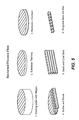
- FIG. 8 is a simplified diagram illustrating a scribe and break operation according to one or more embodiments. This diagram is merely an illustration and should not unduly limit the scope of the claims herein. One of ordinary skill in the art would recognize other variations, modifications, and alternatives.
- the substrates are demounted from the sapphire carrier wafer and cleaned in acetone and isopropyl alcohol according to a specific embodiment.
- the substrates are then mounted onto vinyl tape for the scribe and break process depending upon the embodiment.
- the tape does not leave any residue on the laser bars, which are substantially free from such residues, which are often polymeric in nature or particulates.
- the method includes one or more scribing processes.
- the method includes subjecting the substrates to a laser for pattern formation.
- the pattern is configured for the formation of a pair of facets for one or more ridge lasers.
- the pair of facets face each other and are in parallel alignment with each other.
- the method uses a UV (355 nm) laser to scribe the laser bars.
- the laser is configured on a system, which allows for accurate scribe lines configured in one or more different patterns and profiles.
- the scribing can be performed on the backside, frontside, or both depending upon the application. Of course, there can be other variations, modifications, and alternatives.
- the method uses backside scribing or the like.
- the method preferably forms a continuous line scribe that is perpendicular to the laser bars on the backside of the GaN substrate.
- the scribe is generally 15-20 um deep or other suitable depth.
- backside scribing can be advantageous. That is, the scribe process does not depend on the pitch of the laser bars or other like pattern. Accordingly, backside scribing can lead to a higher density of laser bars on each substrate according to a preferred embodiment.
- backside scribing may lead to residue from the tape on one or more of the facets.
- backside scribe often requires that the substrates face down on the tape. With frontside scribing, the backside of the substrate is in contact with the tape.
- frontside scribing the backside of the substrate is in contact with the tape.
- the present method uses frontside scribing, which facilitates formation of clean facets.
- the frontside scribing process is preferably used.
- the method includes a scribe pattern to produce straight cleaves with minimal facet roughness or other imperfections. Further details of scribing are provided below.
- the pitch of the laser mask is about 200 um, but can be others.
- the method uses a 170 um scribe with a 30 um dash for the 200 um pitch.
- the scribe length is maximized or increased while maintaining the heat affected zone of the laser away from the laser ridge, which is sensitive to heat.
- Scribe Profile A saw tooth profile generally produces minimal facet roughness. It is believed that the saw tooth profile shape creates a very high stress concentration in the material, which causes the cleave to propogate much easier and/or more efficiently.
- the present method provides for a scribe suitable for fabrication of the present laser devices.
- FIG. 9 illustrates cross-sections of substrate materials associated with (1) a backside scribe process; and (2) a frontside scribe process.
- FIG. 9 illustrates cross-sections of substrate materials associated with (1) a backside scribe process; and (2) a frontside scribe process.
- the method includes a breaking process to form a plurality of bar structures.
- This diagram is merely an illustration and should not unduly limit the scope of the claims herein.
- the method uses a breaker to cleave the substrates into bars.
- the breaker has a metal support that has a gap spacing of 900 um.
- the substrate is positioned over the support so that the scribe line is in the centered.
- a suitably sharp ceramic blade then applies pressure directly on the scribe line causing the substrate to cleave along the scribe line.
- FIG. 11 is a simplified diagram illustrating a stacking and coating process according to one or more embodiments. Again, this diagram is merely an illustration and should not unduly limit the scope of the claims herein. One of ordinary skill in the art would recognize other variations, modifications, and alternatives.
- the front facet coating films can be selected from any suitable low reflectance design (AR design).
- the AR design includes a quarterwave coating of Al 2 O 3 capped with a thin layer of HfO 2 according to a specific embodiment.
- the Al 2 O 3 coating is a robust dielectric, and HfO 2 is dense, which helps environmentally passivate and tune the reflectance of the front facet. These coating films are preferably deposited by e beam evaporation.
- the back facet is coated with a high reflectance HR design.
- the HR design includes several quarterwave pairs of SiO 2 /HfO 2 . In a specific embodiment, roughly 6-7 pairs may be used to achieve a reflectance over 99%. Of course, there can be other variations, modifications, and alternatives.
- the method uses a suitable deposition system configured for deposition of each of the facets without breaking vacuum.
- the deposition system includes a dome structure with sufficient height and spatial volume.
- the system allows for the plurality of bars configured in a fixture to be flipped from one side to another side and to expose the back facet and the front facet according to a specific embodiment.
- the method allows for first deposition of the back facet, reconfiguring the bar fixture to expose the front facet, and second deposition of the front facet without breaking vacuum.
- the method allows for deposition of one or more films on front and back without breaking vacuum to save time and improve efficiency.
- Other embodiments can break vacuum.
- FIG. 12 illustrates a method directed to singulate bars into a plurality of die according to a specific embodiment.
- This diagram is merely an illustration and should not unduly limit the scope of the claims herein.
- the method includes testing the laser devices in bar form prior to die singulation.
- the method singulates the bars by performing a scribe and break process (similar to the facet cleave).
- the method forms a shallow continuous line scribe on the top side of the laser bar according to a specific embodiment.
- the width of each die is about 200 um, which may reduce the support gap to 300 um or so.
- the tape is expanded and each of the die is picked off of the tape.
- the method performs a packing operation for each of the die according to one or more embodiments.
- FIG. 13 is a simplified diagram illustrating a laser device according to one or more examples of the present invention.
- the optical device includes a gallium nitride substrate member having a nonpolar crystalline surface region characterized by an orientation of about 1 degree towards (000-1) and less than about 0.3 degrees towards (11-20).
- the bulk nitride GaN substrate comprises nitrogen and has a surface dislocation density below 1E-6 cm ⁇ 2 and a surface roughness of less than 0.2 nm.
- the device has a laser stripe region formed overlying a portion of the nonpolar crystalline orientation surface region.
- the laser stripe region is characterized by a cavity orientation is substantially parallel to the c-direction and has a first end and a second end.
- the device has a first cleaved c-face facet provided on the first end of the laser stripe region and a second cleaved c-face facet provided on the second end of the laser stripe region.
- the first cleaved c-facet is substantially parallel with the second cleaved c-facet.
- Mirror surfaces are formed on each of the cleaved surfaces.
- the first cleaved c-facet comprises a first mirror surface.
- the first mirror surface is provided by a scribing and breaking process such as the one described herein.
- the first mirror surface comprises a reflective coating, which is alumina and hafnia.
- the second cleaved c-facet comprises a second mirror surface.
- the second mirror surface is provided by a scribing and breaking process such as the one described herein.
- the second mirror surface comprises a reflective coating, such as silicon dioxide and hafnia.
- the laser stripe has a length and width. The length is 400-1000 ⁇ m and the width is 1.4-4 ⁇ m. The width is substantially constant in dimension.
- the device is also characterized by a spontaneously emitted light is polarized in substantially perpendicular to the c-direction. That is, the device performs as a laser.
- the spontaneously emitted light is characterized by a polarization ratio perpendicular to the c-direction.
- the spontaneously emitted light characterized by a wavelength of about 405 nanometers to yield blue-violet emission.
- the graph illustrates a power and current relationship for the subject laser device at about 25 Degrees Celsius. Additionally, the wavelength is indicated at about 405 nanometers for the subject laser device.
- the present device is merely an illustration and should not unduly limit the scope of the claims herein.
- One of ordinary skill in the art would recognize other variations, modifications, and alternatives.
- the present invention includes a device and method configured on other gallium and nitrogen containing substrate orientations.
- the gallium and nitrogen containing substrate is configured on a family of planes including a ⁇ 20-21 ⁇ crystal orientation.
- ⁇ 20-21 ⁇ is 14.9 degrees off of the m-plane towards the c-plane (0001).
- the miscut or off-cut angle is +/ ⁇ 17 degrees from the m-plane towards c-plane or alternatively at about the ⁇ 20-21 ⁇ crystal orientation plane.
- the present device includes a laser stripe oriented in a projection of the c-direction, which is perpendicular to the a-direction (or alternatively on the m-plane, it is configured in the c-direction).
- the cleaved facet would be the gallium and nitrogen containing face (e.g., GaN face) that is +/ ⁇ 5 degrees from a direction orthogonal to the projection of the c-direction (or alternatively, for the m-plane laser, it is the c-face).
- GaN face gallium and nitrogen containing face
Abstract
Description
-
- The conventional light bulb is inefficient. More than 90% of the energy used for the conventional light bulb dissipates as thermal, rather than optical, energy.
- The conventional light bulb is not as reliable as it could be, often failing from thermal expansion and contraction of the filament element.
- Conventional light bulbs emit light over a broad spectrum, much of which does not result in bright illumination, and much of which is not perceived due to the spectral sensitivity of the human eye.
- Conventional light bulbs emit in all directions and are not ideal for applications requiring strong directionality or focus such as projection displays, optical data storage, or specialized directed lighting.
-
- 1. Start;
- 2. Provide processed substrate including laser devices with ridges;
- 3. Thin substrate from backside;
- 4. Form backside n-contact;
- 5. Scribe pattern for separation of the laser devices configured in bar structures;
- 6. Break scribed pattern to form a plurality of bar structures;
- 7. Stack bar structures;
- 8. Coat bars structures;
- 9. Singulate bar structures into individual dies having laser device; and
- 10. Perform other steps as desired.
Claims (42)
Priority Applications (15)
| Application Number | Priority Date | Filing Date | Title |
|---|---|---|---|
| US12/759,273 US9531164B2 (en) | 2009-04-13 | 2010-04-13 | Optical device structure using GaN substrates for laser applications |
| US12/868,441 US8634442B1 (en) | 2009-04-13 | 2010-08-25 | Optical device structure using GaN substrates for laser applications |
| US13/549,335 US8837545B2 (en) | 2009-04-13 | 2012-07-13 | Optical device structure using GaN substrates and growth structures for laser applications |
| US14/134,244 US9071039B2 (en) | 2009-04-13 | 2013-12-19 | Optical device structure using GaN substrates for laser applications |
| US14/229,738 US8969113B2 (en) | 2009-04-13 | 2014-03-28 | Optical device structure using GaN substrates and growth structures for laser applications |
| US14/601,651 US9099844B2 (en) | 2009-04-13 | 2015-01-21 | Optical device structure using GaN substrates and growth structures for laser applications |
| US14/736,939 US9722398B2 (en) | 2009-04-13 | 2015-06-11 | Optical device structure using GaN substrates for laser applications |
| US14/754,043 US9356430B2 (en) | 2009-04-13 | 2015-06-29 | Optical device structure using GaN substrates and growth structures for laser applications |
| US15/155,947 US9553426B1 (en) | 2009-04-13 | 2016-05-16 | Optical device structure using GaN substrates and growth structures for laser applications |
| US15/380,156 US9735547B1 (en) | 2009-04-13 | 2016-12-15 | Optical device structure using GaN substrates and growth structures for laser applications |
| US15/671,384 US9941665B1 (en) | 2009-04-13 | 2017-08-08 | Optical device structure using GaN substrates and growth structures for laser applications |
| US15/938,802 US10374392B1 (en) | 2009-04-13 | 2018-03-28 | Optical device structure using GaN substrates and growth structures for laser applications |
| US16/529,587 US10862273B1 (en) | 2009-04-13 | 2019-08-01 | Optical device structure using GaN substrates and growth structures for laser applications |
| US16/799,217 US10862274B1 (en) | 2009-04-13 | 2020-02-24 | Optical device structure using GaN substrates and growth structures for laser applications |
| US17/094,662 US11862937B1 (en) | 2009-04-13 | 2020-11-10 | Optical device structure using GaN substrates and growth structures for laser applications |
Applications Claiming Priority (3)
| Application Number | Priority Date | Filing Date | Title |
|---|---|---|---|
| US16892609P | 2009-04-13 | 2009-04-13 | |
| US24350209P | 2009-09-17 | 2009-09-17 | |
| US12/759,273 US9531164B2 (en) | 2009-04-13 | 2010-04-13 | Optical device structure using GaN substrates for laser applications |
Related Child Applications (4)
| Application Number | Title | Priority Date | Filing Date |
|---|---|---|---|
| US12/762,269 Continuation-In-Part US8254425B1 (en) | 2009-04-13 | 2010-04-16 | Optical device structure using GaN substrates and growth structures for laser applications |
| US12/762,271 Continuation-In-Part US8294179B1 (en) | 2009-04-13 | 2010-04-16 | Optical device structure using GaN substrates and growth structures for laser applications |
| US12/868,441 Continuation-In-Part US8634442B1 (en) | 2009-04-13 | 2010-08-25 | Optical device structure using GaN substrates for laser applications |
| US13/549,335 Continuation-In-Part US8837545B2 (en) | 2009-04-13 | 2012-07-13 | Optical device structure using GaN substrates and growth structures for laser applications |
Publications (2)
| Publication Number | Publication Date |
|---|---|
| US20100316075A1 US20100316075A1 (en) | 2010-12-16 |
| US9531164B2 true US9531164B2 (en) | 2016-12-27 |
Family
ID=42982821
Family Applications (1)
| Application Number | Title | Priority Date | Filing Date |
|---|---|---|---|
| US12/759,273 Active US9531164B2 (en) | 2009-04-13 | 2010-04-13 | Optical device structure using GaN substrates for laser applications |
Country Status (5)
| Country | Link |
|---|---|
| US (1) | US9531164B2 (en) |
| JP (1) | JP5780605B2 (en) |
| CN (1) | CN102396083B (en) |
| DE (1) | DE112010001615T5 (en) |
| WO (1) | WO2010120819A1 (en) |
Cited By (22)
| Publication number | Priority date | Publication date | Assignee | Title |
|---|---|---|---|---|
| US9853420B2 (en) | 2009-09-17 | 2017-12-26 | Soraa Laser Diode, Inc. | Low voltage laser diodes on {20-21} gallium and nitrogen containing substrates |
| US10374392B1 (en) | 2009-04-13 | 2019-08-06 | Soraa Laser Diode, Inc. | Optical device structure using GaN substrates and growth structures for laser applications |
| US10439365B1 (en) | 2014-06-26 | 2019-10-08 | Soraa Laser Diode, Inc. | Epitaxial growth of cladding regions for a gallium and nitrogen containing laser diode |
| US10651629B1 (en) | 2013-06-28 | 2020-05-12 | Soraa Laser Diode, Inc. | Gallium nitride containing laser device configured on a patterned substrate |
| US10655800B2 (en) | 2011-01-24 | 2020-05-19 | Soraa Laser Diode, Inc. | Laser package having multiple emitters configured on a support member |
| US10879674B1 (en) | 2011-10-13 | 2020-12-29 | Soraa Laser Diode, Inc. | Laser devices using a semipolar plane |
| US10903623B2 (en) | 2019-05-14 | 2021-01-26 | Soraa Laser Diode, Inc. | Method and structure for manufacturable large area gallium and nitrogen containing substrate |
| US11005234B1 (en) | 2011-04-04 | 2021-05-11 | Kyocera Sld Laser, Inc. | Laser bar device having multiple emitters |
| US11139634B1 (en) | 2012-04-05 | 2021-10-05 | Kyocera Sld Laser, Inc. | Facet on a gallium and nitrogen containing laser diode |
| US11139637B2 (en) | 2014-02-10 | 2021-10-05 | Kyocera Sld Laser, Inc. | Manufacturable RGB laser diode source and system |
| US11228158B2 (en) | 2019-05-14 | 2022-01-18 | Kyocera Sld Laser, Inc. | Manufacturable laser diodes on a large area gallium and nitrogen containing substrate |
| US11239637B2 (en) | 2018-12-21 | 2022-02-01 | Kyocera Sld Laser, Inc. | Fiber delivered laser induced white light system |
| US11342727B1 (en) | 2014-02-07 | 2022-05-24 | Kyocera Sld Laser, Inc. | Semiconductor laser diode on tiled gallium containing material |
| US11569637B2 (en) | 2013-10-18 | 2023-01-31 | Kyocera Sld Laser, Inc. | Manufacturable laser diode formed on c-plane gallium and nitrogen material |
| US11630307B2 (en) | 2010-05-17 | 2023-04-18 | Kyocera Sld Laser, Inc. | Wearable laser based display method and system |
| US11649936B1 (en) | 2013-12-18 | 2023-05-16 | Kyocera Sld Laser, Inc. | Color converting element for laser device |
| US11658456B2 (en) | 2014-02-10 | 2023-05-23 | Kyocera Sld Laser, Inc. | Manufacturable multi-emitter laser diode |
| US11705689B2 (en) | 2014-02-10 | 2023-07-18 | Kyocera Sld Laser, Inc. | Gallium and nitrogen bearing dies with improved usage of substrate material |
| US11788699B2 (en) | 2018-12-21 | 2023-10-17 | Kyocera Sld Laser, Inc. | Fiber-delivered laser-induced dynamic light system |
| US11862939B1 (en) | 2014-11-06 | 2024-01-02 | Kyocera Sld Laser, Inc. | Ultraviolet laser diode device |
| US11884202B2 (en) | 2019-01-18 | 2024-01-30 | Kyocera Sld Laser, Inc. | Laser-based fiber-coupled white light system |
| US11903187B2 (en) | 2021-04-30 | 2024-02-13 | Samsung Electronics Co., Ltd. | Semiconductor devices |
Families Citing this family (66)
| Publication number | Priority date | Publication date | Assignee | Title |
|---|---|---|---|---|
| US8847249B2 (en) | 2008-06-16 | 2014-09-30 | Soraa, Inc. | Solid-state optical device having enhanced indium content in active regions |
| US20100006873A1 (en) * | 2008-06-25 | 2010-01-14 | Soraa, Inc. | HIGHLY POLARIZED WHITE LIGHT SOURCE BY COMBINING BLUE LED ON SEMIPOLAR OR NONPOLAR GaN WITH YELLOW LED ON SEMIPOLAR OR NONPOLAR GaN |
| US8143148B1 (en) | 2008-07-14 | 2012-03-27 | Soraa, Inc. | Self-aligned multi-dielectric-layer lift off process for laser diode stripes |
| US8805134B1 (en) | 2012-02-17 | 2014-08-12 | Soraa Laser Diode, Inc. | Methods and apparatus for photonic integration in non-polar and semi-polar oriented wave-guided optical devices |
| US8259769B1 (en) | 2008-07-14 | 2012-09-04 | Soraa, Inc. | Integrated total internal reflectors for high-gain laser diodes with high quality cleaved facets on nonpolar/semipolar GaN substrates |
| US8124996B2 (en) | 2008-08-04 | 2012-02-28 | Soraa, Inc. | White light devices using non-polar or semipolar gallium containing materials and phosphors |
| US8284810B1 (en) | 2008-08-04 | 2012-10-09 | Soraa, Inc. | Solid state laser device using a selected crystal orientation in non-polar or semi-polar GaN containing materials and methods |
| US8247886B1 (en) | 2009-03-09 | 2012-08-21 | Soraa, Inc. | Polarization direction of optical devices using selected spatial configurations |
| US8252662B1 (en) | 2009-03-28 | 2012-08-28 | Soraa, Inc. | Method and structure for manufacture of light emitting diode devices using bulk GaN |
| US8422525B1 (en) * | 2009-03-28 | 2013-04-16 | Soraa, Inc. | Optical device structure using miscut GaN substrates for laser applications |
| US8242522B1 (en) | 2009-05-12 | 2012-08-14 | Soraa, Inc. | Optical device structure using non-polar GaN substrates and growth structures for laser applications in 481 nm |
| US8634442B1 (en) | 2009-04-13 | 2014-01-21 | Soraa Laser Diode, Inc. | Optical device structure using GaN substrates for laser applications |
| US8254425B1 (en) | 2009-04-17 | 2012-08-28 | Soraa, Inc. | Optical device structure using GaN substrates and growth structures for laser applications |
| US8294179B1 (en) | 2009-04-17 | 2012-10-23 | Soraa, Inc. | Optical device structure using GaN substrates and growth structures for laser applications |
| JP5780605B2 (en) | 2009-04-13 | 2015-09-16 | ソラア レイザー ダイオード インク | Optical element structure using GAN substrate for laser utilization |
| US8416825B1 (en) | 2009-04-17 | 2013-04-09 | Soraa, Inc. | Optical device structure using GaN substrates and growth structure for laser applications |
| US9250044B1 (en) | 2009-05-29 | 2016-02-02 | Soraa Laser Diode, Inc. | Gallium and nitrogen containing laser diode dazzling devices and methods of use |
| US9800017B1 (en) | 2009-05-29 | 2017-10-24 | Soraa Laser Diode, Inc. | Laser device and method for a vehicle |
| US8427590B2 (en) | 2009-05-29 | 2013-04-23 | Soraa, Inc. | Laser based display method and system |
| US9829780B2 (en) | 2009-05-29 | 2017-11-28 | Soraa Laser Diode, Inc. | Laser light source for a vehicle |
| US10108079B2 (en) | 2009-05-29 | 2018-10-23 | Soraa Laser Diode, Inc. | Laser light source for a vehicle |
| US8247887B1 (en) | 2009-05-29 | 2012-08-21 | Soraa, Inc. | Method and surface morphology of non-polar gallium nitride containing substrates |
| US8509275B1 (en) | 2009-05-29 | 2013-08-13 | Soraa, Inc. | Gallium nitride based laser dazzling device and method |
| US8384300B2 (en) | 2009-09-01 | 2013-02-26 | Topanga Technologies, Inc. | Integrated RF electrodeless plasma lamp device and methods |
| US8314429B1 (en) | 2009-09-14 | 2012-11-20 | Soraa, Inc. | Multi color active regions for white light emitting diode |
| US8750342B1 (en) | 2011-09-09 | 2014-06-10 | Soraa Laser Diode, Inc. | Laser diodes with scribe structures |
| US8933644B2 (en) | 2009-09-18 | 2015-01-13 | Soraa, Inc. | LED lamps with improved quality of light |
| WO2011035265A1 (en) | 2009-09-18 | 2011-03-24 | Soraa, Inc. | Power light emitting diode and method with current density operation |
| US9293644B2 (en) | 2009-09-18 | 2016-03-22 | Soraa, Inc. | Power light emitting diode and method with uniform current density operation |
| US9583678B2 (en) | 2009-09-18 | 2017-02-28 | Soraa, Inc. | High-performance LED fabrication |
| US10147850B1 (en) | 2010-02-03 | 2018-12-04 | Soraa, Inc. | System and method for providing color light sources in proximity to predetermined wavelength conversion structures |
| US8905588B2 (en) | 2010-02-03 | 2014-12-09 | Sorra, Inc. | System and method for providing color light sources in proximity to predetermined wavelength conversion structures |
| EP2543119B1 (en) * | 2010-03-04 | 2020-02-12 | The Regents of The University of California | Semi-polar iii-nitride optoelectronic devices on m-plane gan substrates with miscuts in the ranges 1 to 15 degrees or -1 to -15 degrees in the c-direction |
| US8451876B1 (en) | 2010-05-17 | 2013-05-28 | Soraa, Inc. | Method and system for providing bidirectional light sources with broad spectrum |
| US9450143B2 (en) | 2010-06-18 | 2016-09-20 | Soraa, Inc. | Gallium and nitrogen containing triangular or diamond-shaped configuration for optical devices |
| US8816319B1 (en) | 2010-11-05 | 2014-08-26 | Soraa Laser Diode, Inc. | Method of strain engineering and related optical device using a gallium and nitrogen containing active region |
| US9048170B2 (en) | 2010-11-09 | 2015-06-02 | Soraa Laser Diode, Inc. | Method of fabricating optical devices using laser treatment |
| US8975615B2 (en) * | 2010-11-09 | 2015-03-10 | Soraa Laser Diode, Inc. | Method of fabricating optical devices using laser treatment of contact regions of gallium and nitrogen containing material |
| GB2487531A (en) * | 2011-01-20 | 2012-08-01 | Sharp Kk | Substrate system consisting of a metamorphic transition region comprising a laminate of AlxGa1-x N and the same material as the substrate. |
| JP5553035B2 (en) * | 2011-01-24 | 2014-07-16 | 住友電気工業株式会社 | Gallium nitride semiconductor laser device |
| US9595813B2 (en) * | 2011-01-24 | 2017-03-14 | Soraa Laser Diode, Inc. | Laser package having multiple emitters configured on a substrate member |
| US9093820B1 (en) | 2011-01-25 | 2015-07-28 | Soraa Laser Diode, Inc. | Method and structure for laser devices using optical blocking regions |
| JP5716524B2 (en) * | 2011-05-06 | 2015-05-13 | 日亜化学工業株式会社 | Method for manufacturing light emitting device |
| US8686431B2 (en) | 2011-08-22 | 2014-04-01 | Soraa, Inc. | Gallium and nitrogen containing trilateral configuration for optical devices |
| CN102522318B (en) * | 2011-12-30 | 2013-11-27 | 厦门大学 | Self-splitting and transfer method for GaN-based epitaxial film |
| US9020003B1 (en) | 2012-03-14 | 2015-04-28 | Soraa Laser Diode, Inc. | Group III-nitride laser diode grown on a semi-polar orientation of gallium and nitrogen containing substrates |
| US9343871B1 (en) | 2012-04-05 | 2016-05-17 | Soraa Laser Diode, Inc. | Facet on a gallium and nitrogen containing laser diode |
| US9800016B1 (en) | 2012-04-05 | 2017-10-24 | Soraa Laser Diode, Inc. | Facet on a gallium and nitrogen containing laser diode |
| US9099843B1 (en) | 2012-07-19 | 2015-08-04 | Soraa Laser Diode, Inc. | High operating temperature laser diodes |
| US8971368B1 (en) | 2012-08-16 | 2015-03-03 | Soraa Laser Diode, Inc. | Laser devices having a gallium and nitrogen containing semipolar surface orientation |
| US9184563B1 (en) * | 2012-08-30 | 2015-11-10 | Soraa Laser Diode, Inc. | Laser diodes with an etched facet and surface treatment |
| US9978904B2 (en) | 2012-10-16 | 2018-05-22 | Soraa, Inc. | Indium gallium nitride light emitting devices |
| US9379525B2 (en) | 2014-02-10 | 2016-06-28 | Soraa Laser Diode, Inc. | Manufacturable laser diode |
| US9520695B2 (en) | 2013-10-18 | 2016-12-13 | Soraa Laser Diode, Inc. | Gallium and nitrogen containing laser device having confinement region |
| US9419189B1 (en) | 2013-11-04 | 2016-08-16 | Soraa, Inc. | Small LED source with high brightness and high efficiency |
| US9653642B1 (en) | 2014-12-23 | 2017-05-16 | Soraa Laser Diode, Inc. | Manufacturable RGB display based on thin film gallium and nitrogen containing light emitting diodes |
| US9666677B1 (en) | 2014-12-23 | 2017-05-30 | Soraa Laser Diode, Inc. | Manufacturable thin film gallium and nitrogen containing devices |
| US10938182B2 (en) | 2015-08-19 | 2021-03-02 | Soraa Laser Diode, Inc. | Specialized integrated light source using a laser diode |
| US10879673B2 (en) | 2015-08-19 | 2020-12-29 | Soraa Laser Diode, Inc. | Integrated white light source using a laser diode and a phosphor in a surface mount device package |
| US11437775B2 (en) | 2015-08-19 | 2022-09-06 | Kyocera Sld Laser, Inc. | Integrated light source using a laser diode |
| US11437774B2 (en) | 2015-08-19 | 2022-09-06 | Kyocera Sld Laser, Inc. | High-luminous flux laser-based white light source |
| US9787963B2 (en) | 2015-10-08 | 2017-10-10 | Soraa Laser Diode, Inc. | Laser lighting having selective resolution |
| CN109154697B (en) * | 2016-05-20 | 2020-11-10 | 镁可微波技术有限公司 | Semiconductor laser and method for planarizing semiconductor laser |
| US10771155B2 (en) | 2017-09-28 | 2020-09-08 | Soraa Laser Diode, Inc. | Intelligent visible light with a gallium and nitrogen containing laser source |
| US10222474B1 (en) | 2017-12-13 | 2019-03-05 | Soraa Laser Diode, Inc. | Lidar systems including a gallium and nitrogen containing laser light source |
| US10551728B1 (en) | 2018-04-10 | 2020-02-04 | Soraa Laser Diode, Inc. | Structured phosphors for dynamic lighting |
Citations (253)
| Publication number | Priority date | Publication date | Assignee | Title |
|---|---|---|---|---|
| US4318058A (en) | 1979-04-24 | 1982-03-02 | Nippon Electric Co., Ltd. | Semiconductor diode laser array |
| US4341592A (en) | 1975-08-04 | 1982-07-27 | Texas Instruments Incorporated | Method for removing photoresist layer from substrate by ozone treatment |
| US4860687A (en) | 1986-03-21 | 1989-08-29 | U.S. Philips Corporation | Device comprising a flat susceptor rotating parallel to a reference surface about a shift perpendicular to this surface |
| US4911102A (en) | 1987-01-31 | 1990-03-27 | Toyoda Gosei Co., Ltd. | Process of vapor growth of gallium nitride and its apparatus |
| JPH03287770A (en) | 1990-04-05 | 1991-12-18 | Hitachi Electron Eng Co Ltd | Single wafer processing atmospheric cvd device |
| US5331654A (en) | 1993-03-05 | 1994-07-19 | Photonics Research Incorporated | Polarized surface-emitting laser |
| US5334277A (en) | 1990-10-25 | 1994-08-02 | Nichia Kagaky Kogyo K.K. | Method of vapor-growing semiconductor crystal and apparatus for vapor-growing the same |
| US5366953A (en) | 1991-03-19 | 1994-11-22 | Conductus, Inc. | Method of forming grain boundary junctions in high temperature superconductor films |
| US5527417A (en) | 1992-07-06 | 1996-06-18 | Kabushiki Kaisha Toshiba | Photo-assisted CVD apparatus |
| US5607899A (en) | 1994-02-25 | 1997-03-04 | Sumitomo Electric Industries, Ltd. | Method of forming single-crystalline thin film |
| US5632812A (en) | 1993-03-10 | 1997-05-27 | Canon Kabushiki Kaisha | Diamond electronic device and process for producing the same |
| US5647945A (en) | 1993-08-25 | 1997-07-15 | Tokyo Electron Limited | Vacuum processing apparatus |
| US5696389A (en) | 1994-03-15 | 1997-12-09 | Kabushiki Kaisha Toshiba | Light-emitting semiconductor device |
| US5760484A (en) * | 1997-02-11 | 1998-06-02 | Mosel Vitelic Inc. | Alignment mark pattern for semiconductor process |
| US5821555A (en) | 1995-03-27 | 1998-10-13 | Kabushiki Kaisha Toshiba | Semicoductor device having a hetero interface with a lowered barrier |
| US5888907A (en) | 1996-04-26 | 1999-03-30 | Tokyo Electron Limited | Plasma processing method |
| US5926493A (en) | 1997-05-20 | 1999-07-20 | Sdl, Inc. | Optical semiconductor device with diffraction grating structure |
| US5951923A (en) | 1996-05-23 | 1999-09-14 | Ebara Corporation | Vaporizer apparatus and film deposition apparatus therewith |
| US6069394A (en) | 1997-04-09 | 2000-05-30 | Matsushita Electronics Corporation | Semiconductor substrate, semiconductor device and method of manufacturing the same |
| US6072197A (en) | 1996-02-23 | 2000-06-06 | Fujitsu Limited | Semiconductor light emitting device with an active layer made of semiconductor having uniaxial anisotropy |
| US6147953A (en) | 1998-03-25 | 2000-11-14 | Duncan Technologies, Inc. | Optical signal transmission apparatus |
| US6153010A (en) | 1997-04-11 | 2000-11-28 | Nichia Chemical Industries Ltd. | Method of growing nitride semiconductors, nitride semiconductor substrate and nitride semiconductor device |
| US6195381B1 (en) | 1998-04-27 | 2001-02-27 | Wisconsin Alumni Research Foundation | Narrow spectral width high-power distributed feedback semiconductor lasers |
| US6239454B1 (en) | 1999-05-10 | 2001-05-29 | Lucent Technologies Inc. | Net strain reduction in integrated laser-modulator |
| US20010048114A1 (en) | 1997-06-03 | 2001-12-06 | Etsuo Morita | Semiconductor substrate and semiconductor device |
| US20020027933A1 (en) | 2000-07-18 | 2002-03-07 | Rohm Co., Ltd. | Semiconductor light emitting device and semiconductor laser |
| US6379985B1 (en) * | 2001-08-01 | 2002-04-30 | Xerox Corporation | Methods for cleaving facets in III-V nitrides grown on c-face sapphire substrates |
| US20020050488A1 (en) | 2000-03-01 | 2002-05-02 | Dmitri Nikitin | Method and apparatus for thermally processing quartz using a plurality of laser beams |
| US20020085603A1 (en) | 1997-03-07 | 2002-07-04 | Toshiyuki Okumura | Gallium nitride semiconductor light emitting device having multi-quantum-well structure active layer, and semiconductor laser light source device |
| US20020105986A1 (en) | 2000-12-20 | 2002-08-08 | Yukio Yamasaki | Semiconductor laser device and method of manufacturing the same |
| US6451157B1 (en) | 1999-09-23 | 2002-09-17 | Lam Research Corporation | Gas distribution apparatus for semiconductor processing |
| US20020171092A1 (en) | 2001-03-29 | 2002-11-21 | Goetz Werner K. | Indium gallium nitride smoothing structures for III-nitride devices |
| US6489636B1 (en) | 2001-03-29 | 2002-12-03 | Lumileds Lighting U.S., Llc | Indium gallium nitride smoothing structures for III-nitride devices |
| US20030001238A1 (en) | 2001-06-06 | 2003-01-02 | Matsushita Electric Industrial Co., Ltd. | GaN-based compound semiconductor EPI-wafer and semiconductor element using the same |
| US20030000453A1 (en) | 2001-06-27 | 2003-01-02 | Yasuyuki Unno | Optical element and manufacturing method thereof |
| US20030012243A1 (en) | 1998-01-26 | 2003-01-16 | Toshiyuki Okumura | Gallium nitride type semiconductor laser device |
| US20030020087A1 (en) | 2001-04-24 | 2003-01-30 | Osamu Goto | Nitride semiconductor, semiconductor device, and method of manufacturing the same |
| US6586762B2 (en) | 2000-07-07 | 2003-07-01 | Nichia Corporation | Nitride semiconductor device with improved lifetime and high output power |
| US20030129810A1 (en) | 2000-05-30 | 2003-07-10 | Barth Kurt L. | Apparatus and processes for the mass production of photovoltaic modules |
| US20030140846A1 (en) | 2002-01-17 | 2003-07-31 | Goshi Biwa | Selective growth method, and semiconductor light emitting device and fabrication method thereof |
| US20030178617A1 (en) | 2002-03-20 | 2003-09-25 | International Business Machines Corporation | Self-aligned nanotube field effect transistor and method of fabricating same |
| US6639925B2 (en) | 1996-10-30 | 2003-10-28 | Hitachi, Inc. | Optical information processing equipment and semiconductor light emitting device suitable therefor |
| US20030200931A1 (en) | 2000-04-17 | 2003-10-30 | Goodwin Dennis L. | Rotating semiconductor processing apparatus |
| US20030216011A1 (en) | 1992-11-20 | 2003-11-20 | Nichia Chemical Industries Ltd. | Light-emitting gallium nitride-based compound semiconductor device |
| US20040025787A1 (en) | 2002-04-19 | 2004-02-12 | Selbrede Steven C. | System for depositing a film onto a substrate using a low pressure gas precursor |
| US20040060518A1 (en) | 2001-09-29 | 2004-04-01 | Cree Lighting Company | Apparatus for inverted multi-wafer MOCVD fabrication |
| US6734461B1 (en) | 1999-09-07 | 2004-05-11 | Sixon Inc. | SiC wafer, SiC semiconductor device, and production method of SiC wafer |
| US20040099213A1 (en) | 2000-07-24 | 2004-05-27 | Adomaitis Raymond A | Spatially programmable microelectronics process equipment using segmented gas injection showerhead with exhaust gas recirculation |
| US20040104391A1 (en) | 2001-09-03 | 2004-06-03 | Toshihide Maeda | Semiconductor light emitting device, light emitting apparatus and production method for semiconductor light emitting device |
| US6755932B2 (en) | 2000-02-21 | 2004-06-29 | Hitachi, Ltd. | Plasma processing system and apparatus and a sample processing method |
| US20040146264A1 (en) | 2000-06-16 | 2004-07-29 | Auner Gregory W. | Wide bandgap semiconductor waveguide structures |
| US20040151222A1 (en) | 2003-02-05 | 2004-08-05 | Fujitsu Limited | Distributed feedback semiconductor laser |
| US20040196877A1 (en) | 2003-04-01 | 2004-10-07 | Sharp Kabushiki Kaisha | Multi-wavelength laser device |
| CN1538534A (en) | 2003-04-15 | 2004-10-20 | 郑荣彬 | White light illuminating device |
| US6809781B2 (en) | 2002-09-24 | 2004-10-26 | General Electric Company | Phosphor blends and backlight sources for liquid crystal displays |
| US6814811B2 (en) | 1998-10-29 | 2004-11-09 | Shin-Etsu Handotai Co., Ltd. | Semiconductor wafer and vapor phase growth apparatus |
| US20040222357A1 (en) | 2002-05-22 | 2004-11-11 | King David Andrew | Optical excitation/detection device and method for making same using fluidic self-assembly techniques |
| US20040233950A1 (en) | 2001-06-15 | 2004-11-25 | Yoshihiko Furukawa | Semicondutor laser device and its manufacturing method |
| WO2004084275A3 (en) | 2003-03-18 | 2004-12-09 | Crystal Photonics Inc | Method for making group iii nitride devices and devices produced thereby |
| US20040247275A1 (en) | 2003-03-12 | 2004-12-09 | Daryoosh Vakhshoori | Extended optical bandwidth semiconductor source |
| US6833564B2 (en) | 2001-11-02 | 2004-12-21 | Lumileds Lighting U.S., Llc | Indium gallium nitride separate confinement heterostructure light emitting devices |
| US20040262624A1 (en) | 2003-06-26 | 2004-12-30 | Katsushi Akita | GaN substrate and method of fabricating the same, nitride semiconductor device and method of fabricating the same |
| US6858882B2 (en) | 2000-09-08 | 2005-02-22 | Sharp Kabushiki Kaisha | Nitride semiconductor light-emitting device and optical device including the same |
| US20050040384A1 (en) | 2003-08-20 | 2005-02-24 | Kabushiki Kaisha Toshiba | Semiconductor light-emitting element and method of manufacturing the same |
| US20050072986A1 (en) | 2001-09-03 | 2005-04-07 | Nec Corporation | Group-III nitride semiconductor device |
| US6920166B2 (en) | 2002-03-19 | 2005-07-19 | Nippon Telegraph & Telephone Corporation | Thin film deposition method of nitride semiconductor and nitride semiconductor light emitting device |
| US20050168564A1 (en) | 2004-01-30 | 2005-08-04 | Yoshinobu Kawaguchi | Method and device for driving LED element, illumination apparatus, and display apparatus |
| US20050214992A1 (en) | 2002-12-16 | 2005-09-29 | The Regents Of The University Of California | Fabrication of nonpolar indium gallium nitride thin films, heterostructures and devices by metalorganic chemical vapor deposition |
| US20050218413A1 (en) | 2001-12-27 | 2005-10-06 | Fuji Photo Film Co., Ltd. | Image exposure device and laser exposure device applied thereto |
| US20050224826A1 (en) | 2004-03-19 | 2005-10-13 | Lumileds Lighting, U.S., Llc | Optical system for light emitting diodes |
| US20050229855A1 (en) | 1998-09-10 | 2005-10-20 | Ivo Raaijmakers | Apparatus for thermal treatment of substrates |
| US20050230701A1 (en) | 2004-04-16 | 2005-10-20 | Wen-Chieh Huang | High brightness gallium nitride-based light emitting diode with transparent conducting oxide spreading layer |
| US20050247260A1 (en) | 2004-05-07 | 2005-11-10 | Hyunmin Shin | Non-polar single crystalline a-plane nitride semiconductor wafer and preparation thereof |
| US20050285128A1 (en) | 2004-02-10 | 2005-12-29 | California Institute Of Technology | Surface plasmon light emitter structure and method of manufacture |
| US20050286591A1 (en) | 2004-06-25 | 2005-12-29 | Samsung Electro-Mechanics Co., Ltd. | Method of producing multi-wavelength semiconductor laser device |
| US20060030738A1 (en) | 2004-08-06 | 2006-02-09 | Luc Vanmaele | Device provided with a dedicated dye compound |
| US20060033009A1 (en) | 2004-08-16 | 2006-02-16 | Shuichi Kobayashi | Displaying optical system and image projection apparatus |
| US20060038193A1 (en) | 2004-08-18 | 2006-02-23 | Liang-Wen Wu | Gallium-nitride based light emitting diode structure with enhanced light illuminance |
| US20060037529A1 (en) | 2002-03-27 | 2006-02-23 | General Electric Company | Single crystal and quasi-single crystal, composition, apparatus, and associated method |
| US7009199B2 (en) | 2002-10-22 | 2006-03-07 | Cree, Inc. | Electronic devices having a header and antiparallel connected light emitting diodes for producing light from AC current |
| US20060060131A1 (en) | 2003-12-29 | 2006-03-23 | Translucent, Inc. | Method of forming a rare-earth dielectric layer |
| US7019325B2 (en) | 2004-06-16 | 2006-03-28 | Exalos Ag | Broadband light emitting device |
| US20060066319A1 (en) | 2004-09-29 | 2006-03-30 | Loadstar Sensors.Inc. | Area-change sensing through capacitive techniques |
| US20060077795A1 (en) | 2004-09-01 | 2006-04-13 | Fujinon Corporation | Objective optical system for optical recording media and optical pickup device using it |
| US20060079082A1 (en) | 2002-07-19 | 2006-04-13 | Cree, Inc. | Trench cut light emitting diodes and methods of fabricating same |
| US20060078024A1 (en) * | 2004-03-05 | 2006-04-13 | Hiroaki Matsumura | Semiconductor laser device |
| US20060078022A1 (en) | 1999-03-04 | 2006-04-13 | Tokuya Kozaki | Nitride semiconductor laser device |
| US20060086319A1 (en) | 2003-06-10 | 2006-04-27 | Tokyo Electron Limited | Processing gas supply mechanism, film forming apparatus and method, and computer storage medium storing program for controlling same |
| US7053413B2 (en) | 2000-10-23 | 2006-05-30 | General Electric Company | Homoepitaxial gallium-nitride-based light emitting device and method for producing |
| CN1781195A (en) | 2003-03-18 | 2006-05-31 | 克利斯托光子学公司 | Method for making group III nitride devices and devices produced thereby |
| US20060118799A1 (en) | 2003-10-24 | 2006-06-08 | General Electric Company | Resonant cavity light emitting devices and associated method |
| US20060126688A1 (en) | 2004-12-14 | 2006-06-15 | Palo Alto Research Center Incorporated | Blue and green laser diodes with gallium nitride or indium gallium nitride cladding laser structure |
| US20060144334A1 (en) | 2002-05-06 | 2006-07-06 | Applied Materials, Inc. | Method and apparatus for deposition of low dielectric constant materials |
| US20060175624A1 (en) | 2005-02-09 | 2006-08-10 | The Regents Of The University Of California | Semiconductor light-emitting device |
| US20060189098A1 (en) | 2005-02-23 | 2006-08-24 | Cree, Inc. | Substrate removal process for high light extraction LEDs |
| US20060193359A1 (en) | 2005-02-25 | 2006-08-31 | Mitsubishi Denki Kabushiki Kaisha | Semiconductor light-emitting device |
| US20060205199A1 (en) | 2005-03-10 | 2006-09-14 | The Regents Of The University Of California | Technique for the growth of planar semi-polar gallium nitride |
| US20060213429A1 (en) | 2001-10-09 | 2006-09-28 | Sumitomo Electric Industries, Ltd. | Single crystal GaN substrate, method of growing single crystal GaN and method of producing single crystal GaN substrate |
| US20060216416A1 (en) | 2003-04-16 | 2006-09-28 | Sumakeris Joseph J | Methods for controlling formation of deposits in a deposition system and deposition methods including the same |
| US7128849B2 (en) | 2003-10-31 | 2006-10-31 | General Electric Company | Phosphors containing boron and metals of Group IIIA and IIIB |
| US20060256482A1 (en) | 2005-05-10 | 2006-11-16 | Hitachi Global Storage Technologies Netherlands, B.V. | Method to fabricate side shields for a magnetic sensor |
| US20060288928A1 (en) | 2005-06-10 | 2006-12-28 | Chang-Beom Eom | Perovskite-based thin film structures on miscut semiconductor substrates |
| JP2007068398A (en) | 1999-01-13 | 2007-03-15 | Shinko Electric Co Ltd | Automatic guided vehicle system |
| US20070081857A1 (en) | 2005-10-07 | 2007-04-12 | Yoon Jung H | Four parts manhole enabling an easy install and height adjustment |
| US20070086916A1 (en) | 2005-10-14 | 2007-04-19 | General Electric Company | Faceted structure, article, sensor device, and method |
| US20070093073A1 (en) | 2005-06-01 | 2007-04-26 | Farrell Robert M Jr | Technique for the growth and fabrication of semipolar (Ga,A1,In,B)N thin films, heterostructures, and devices |
| US20070101932A1 (en) | 2001-12-24 | 2007-05-10 | Crystal Is, Inc. | Method and apparatus for producing large, single-crystals of aluminum nitride |
| US20070110112A1 (en) | 2005-11-16 | 2007-05-17 | Katsumi Sugiura | Group III nitride semiconductor light emitting device |
| US20070120141A1 (en) | 2004-04-15 | 2007-05-31 | Moustakas Theodore D | Optical devices featuring textured semiconductor layers |
| JP2007173467A (en) | 2005-12-21 | 2007-07-05 | Toyota Motor Corp | Semiconductor thin-film manufacturing equipment |
| US20070153866A1 (en) | 2004-07-30 | 2007-07-05 | Shchegrov Andrei V | Manufacturable vertical extended cavity surface emitting laser arrays |
| US20070163490A1 (en) | 2005-12-22 | 2007-07-19 | Freiberger Compound Materials Gmbh | Process for selective masking of iii-n layers and for the preparation of free-standing iii-n layers or of devices, and products obtained thereby |
| US20070166853A1 (en) | 2004-04-30 | 2007-07-19 | Guenther Ewald K M | LED Arrangement |
| CN101009347A (en) | 2006-01-27 | 2007-08-01 | 中国科学院物理研究所 | Non polarity A side nitride film growing on the silicon(102) substrate and its making method and use |
| US20070184637A1 (en) | 2004-06-03 | 2007-08-09 | The Regents Of The University Of California | Growth of planar reduced dislocation density m-plane gallium nitride by hydride vapor phase epitaxy |
| US20070217462A1 (en) | 2006-03-14 | 2007-09-20 | Sharp Kabushiki Kaisha | Nitride semiconductor laser device and method of producing the same |
| US20070242716A1 (en) | 2004-03-19 | 2007-10-18 | Arizona Board Of Regents, A Body Corporation Acting On Behalf Of Arizona State University | High Power Vcsels With Transverse Mode Control |
| US20070252164A1 (en) | 2006-02-17 | 2007-11-01 | Hong Zhong | METHOD FOR GROWTH OF SEMIPOLAR (Al,In,Ga,B)N OPTOELECTRONIC DEVICES |
| US20070259464A1 (en) | 2006-05-05 | 2007-11-08 | Applied Materials, Inc. | Dislocation-specific dielectric mask deposition and lateral epitaxial overgrowth to reduce dislocation density of nitride films |
| CN101079463A (en) | 2006-05-23 | 2007-11-28 | Lg.菲利浦Lcd株式会社 | Light-emitting diode chip for backlight unit, manufacturing method thereof, and liquid crystal display device including the same |
| US7303630B2 (en) | 2003-11-05 | 2007-12-04 | Sumitomo Electric Industries, Ltd. | Method of growing GaN crystal, method of producing single crystal GaN substrate, and single crystal GaN substrate |
| US20070280320A1 (en) | 2006-05-15 | 2007-12-06 | Feezell Daniel F | Electrically-pumped (Ga,In,Al)N vertical-cavity surface-emitting laser |
| US7312156B2 (en) | 1996-07-08 | 2007-12-25 | Asm International N.V. | Method and apparatus for supporting a semiconductor wafer during processing |
| CN101099245A (en) | 2005-01-10 | 2008-01-02 | 克利公司 | Light emission device |
| US7323723B2 (en) | 2001-12-28 | 2008-01-29 | Sanken Electric Co., Ltd. | Semiconductor light-emitting device using phosphors for performing wavelength conversion |
| US20080029152A1 (en) | 2006-08-04 | 2008-02-07 | Erel Milshtein | Laser scribing apparatus, systems, and methods |
| US7338828B2 (en) | 2005-05-31 | 2008-03-04 | The Regents Of The University Of California | Growth of planar non-polar {1 -1 0 0} m-plane gallium nitride with metalorganic chemical vapor deposition (MOCVD) |
| WO2008041521A1 (en) | 2006-09-29 | 2008-04-10 | Rohm Co., Ltd. | Light-emitting device |
| US7358542B2 (en) | 2005-02-02 | 2008-04-15 | Lumination Llc | Red emitting phosphor materials for use in LED and LCD applications |
| US7358543B2 (en) | 2005-05-27 | 2008-04-15 | Avago Technologies Ecbu Ip (Singapore) Pte. Ltd. | Light emitting device having a layer of photonic crystals and a region of diffusing material and method for fabricating the device |
| US20080087919A1 (en) | 2006-10-08 | 2008-04-17 | Tysoe Steven A | Method for forming nitride crystals |
| US20080094592A1 (en) | 2006-08-31 | 2008-04-24 | Nikon Corporation | Movable body drive method and movable body drive system, pattern formation method and apparatus, exposure method and apparatus, and device manufacturing method |
| US20080092812A1 (en) | 2004-06-10 | 2008-04-24 | Mcdiarmid James | Methods and Apparatuses for Depositing Uniform Layers |
| US20080095492A1 (en) | 2006-10-18 | 2008-04-24 | Samsung Electronics Co., Ltd. | Semiconductor optoelectronic device and method of fabricating the same |
| CN101171692A (en) | 2005-05-02 | 2008-04-30 | 韩国化学研究院 | Preparation of white light emitting diode using a phosphor |
| US20080124817A1 (en) | 2006-08-23 | 2008-05-29 | Applied Materials, Inc. | Stress measurement and stress balance in films |
| US20080121916A1 (en) | 2006-11-24 | 2008-05-29 | Agency For Science, Technology And Research | Method of forming a metal contact and passivation of a semiconductor feature |
| US7390359B2 (en) | 2004-10-06 | 2008-06-24 | Sumitomo Electric Industries, Ltd. | Nitride semiconductor wafer |
| US20080149949A1 (en) | 2006-12-11 | 2008-06-26 | The Regents Of The University Of California | Lead frame for transparent and mirrorless light emitting diodes |
| US20080149959A1 (en) | 2006-12-11 | 2008-06-26 | The Regents Of The University Of California | Transparent light emitting diodes |
| US20080164578A1 (en) | 2006-12-28 | 2008-07-10 | Saint-Gobain Ceramics & Plastics, Inc. | Sapphire substrates and methods of making same |
| US20080173735A1 (en) | 2007-01-12 | 2008-07-24 | Veeco Instruments Inc. | Gas treatment systems |
| US20080191192A1 (en) | 2007-02-12 | 2008-08-14 | The Regents Of The University Of California | Al(x)Ga(1-x)N-CLADDING-FREE NONPOLAR III-NITRIDE BASED LASER DIODES AND LIGHT EMITTING DIODES |
| US20080191223A1 (en) | 2007-02-12 | 2008-08-14 | The Regents Of The University Of California | CLEAVED FACET (Ga,Al,In)N EDGE-EMITTING LASER DIODES GROWN ON SEMIPOLAR BULK GALLIUM NITRIDE SUBSTRATES |
| US20080198881A1 (en) | 2007-02-12 | 2008-08-21 | The Regents Of The University Of California | OPTIMIZATION OF LASER BAR ORIENTATION FOR NONPOLAR AND SEMIPOLAR (Ga,Al,In,B)N DIODE LASERS |
| US20080210958A1 (en) | 2006-12-05 | 2008-09-04 | Rohm Co., Ltd. | Semiconductor white light emitting device and method for manufacturing the same |
| JP2008205231A (en) | 2007-02-21 | 2008-09-04 | Sharp Corp | Nitride-based semiconductor light-emitting element and manufacturing method therefor |
| US20080217745A1 (en) | 2006-12-19 | 2008-09-11 | Sumitomo Electric Industries, Ltd. | Nitride Semiconductor Wafer |
| US20080232416A1 (en) | 2007-03-23 | 2008-09-25 | Rohm Co., Ltd. | Light emitting device |
| US20080251020A1 (en) | 2005-11-19 | 2008-10-16 | Walter Franken | Cvd-Reactor with Slidingly Mounted Susceptor Holder |
| US20080283851A1 (en) | 2007-05-17 | 2008-11-20 | Sumitomo Electric Industries, Ltd. | GaN Substrate, and Epitaxial Substrate and Semiconductor Light-Emitting Device Employing the Substrate |
| US20080285609A1 (en) * | 2007-05-16 | 2008-11-20 | Rohm Co., Ltd. | Semiconductor laser diode |
| US20080291961A1 (en) | 2005-12-16 | 2008-11-27 | Takeshi Kamikawa | Nitride semiconductor light emitting device and method of fabricating nitride semiconductor laser device |
| US20080298409A1 (en) | 2007-05-31 | 2008-12-04 | Sharp Kabushiki Kaisha | Nitride semiconductor laser chip and fabrication method thereof |
| US20080303033A1 (en) | 2007-06-05 | 2008-12-11 | Cree, Inc. | Formation of nitride-based optoelectronic and electronic device structures on lattice-matched substrates |
| JP2008300547A (en) | 2007-05-30 | 2008-12-11 | Sanyo Electric Co Ltd | Nitride semiconductor laser element and its manufacturing method |
| JP2008306062A (en) | 2007-06-08 | 2008-12-18 | Rohm Co Ltd | Semiconductor light-emitting element and its fabrication process |
| US20080308815A1 (en) | 2007-06-14 | 2008-12-18 | Sumitomo Electric Industries, Ltd. | GaN Substrate, Substrate with an Epitaxial Layer, Semiconductor Device, and GaN Substrate Manufacturing Method |
| US20080315179A1 (en) | 2007-06-22 | 2008-12-25 | Tae Yun Kim | Semiconductor light emitting device |
| US7470555B2 (en) | 2000-06-08 | 2008-12-30 | Nichia Corporation | Semiconductor laser device, and method of manufacturing the same |
| US20090021723A1 (en) | 2007-07-19 | 2009-01-22 | Zygo Corporation | Generating model signals for interferometry |
| US7483468B2 (en) | 2006-01-27 | 2009-01-27 | Kabushiki Kaisha Toshiba | Multiple wavelengths semiconductor laser device |
| US7483466B2 (en) | 2005-04-28 | 2009-01-27 | Canon Kabushiki Kaisha | Vertical cavity surface emitting laser device |
| US7489441B2 (en) | 2004-05-17 | 2009-02-10 | Carl Zeiss Smt Ag | Monocrystalline optical component with curved surface and multilayer coating |
| US7491984B2 (en) | 2000-03-31 | 2009-02-17 | Toyoda Gosei Co., Ltd. | Method for fabricating group III nitride compound semiconductors and group III nitride compound semiconductor devices |
| US20090061857A1 (en) | 2007-08-28 | 2009-03-05 | Cingular Wireless Ii, Llc | Determining capability to provide dynamic local time updates in a prepaid terminating call |
| US20090058532A1 (en) | 2007-08-31 | 2009-03-05 | Fujitsu Limited | Nitride semiconductor device, doherty amplifier and drain voltage controlled amplifier |
| US20090066241A1 (en) | 2006-09-12 | 2009-03-12 | Konica Minolta Holdings ,Inc. | Organic electroluminescence element, and illuminating device and display device therewith |
| US20090078944A1 (en) | 2007-09-07 | 2009-03-26 | Rohm Co., Ltd. | Light emitting device and method of manufacturing the same |
| US20090080857A1 (en) | 2007-09-21 | 2009-03-26 | Echostar Technologies Corporation | Systems and methods for selectively recording at least part of a program based on an occurrence of a video or audio characteristic in the program |
| US20090081857A1 (en) * | 2007-09-14 | 2009-03-26 | Kyma Technologies, Inc. | Non-polar and semi-polar GaN substrates, devices, and methods for making them |
| US20090081867A1 (en) | 2007-09-21 | 2009-03-26 | Shinko Electric Industries Co., Ltd. | Method of manufacturing substrate |
| US20090141765A1 (en) | 2007-11-12 | 2009-06-04 | Rohm Co., Ltd. | Nitride semiconductor laser device |
| US20090153752A1 (en) | 2007-12-14 | 2009-06-18 | Silverstein Barry D | Projector using independent multiple wavelength light sources |
| US20090159869A1 (en) | 2005-03-11 | 2009-06-25 | Ponce Fernando A | Solid State Light Emitting Device |
| US7555025B2 (en) | 2007-03-07 | 2009-06-30 | Mitsubishi Electric Corporation | Semiconductor laser device |
| US20090250686A1 (en) | 2008-04-04 | 2009-10-08 | The Regents Of The University Of California | METHOD FOR FABRICATION OF SEMIPOLAR (Al, In, Ga, B)N BASED LIGHT EMITTING DIODES |
| US20090267100A1 (en) | 2008-04-25 | 2009-10-29 | Sanyo Electric Co., Ltd. | Nitride-based semiconductor device and method of manufacturing the same |
| US20090273005A1 (en) | 2006-07-24 | 2009-11-05 | Hung-Yi Lin | Opto-electronic package structure having silicon-substrate and method of forming the same |
| US20090301387A1 (en) | 2008-06-05 | 2009-12-10 | Soraa Inc. | High pressure apparatus and method for nitride crystal growth |
| US20090301388A1 (en) | 2008-06-05 | 2009-12-10 | Soraa Inc. | Capsule for high pressure processing and method of use for supercritical fluids |
| US20090309110A1 (en) | 2008-06-16 | 2009-12-17 | Soraa, Inc. | Selective area epitaxy growth method and structure for multi-colored devices |
| US20090309127A1 (en) | 2008-06-13 | 2009-12-17 | Soraa, Inc. | Selective area epitaxy growth method and structure |
| US20090310640A1 (en) | 2008-04-04 | 2009-12-17 | The Regents Of The University Of California | MOCVD GROWTH TECHNIQUE FOR PLANAR SEMIPOLAR (Al, In, Ga, B)N BASED LIGHT EMITTING DIODES |
| US20090316116A1 (en) | 2008-05-19 | 2009-12-24 | University Of Washington Uw Techtransfer - Invention Licensing | Scanning laser projection display for small handheld devices |
| US20090320744A1 (en) | 2008-06-18 | 2009-12-31 | Soraa, Inc. | High pressure apparatus and method for nitride crystal growth |
| US20090321778A1 (en) | 2008-06-30 | 2009-12-31 | Advanced Optoelectronic Technology, Inc. | Flip-chip light emitting diode and method for fabricating the same |
| US20100003492A1 (en) | 2008-07-07 | 2010-01-07 | Soraa, Inc. | High quality large area bulk non-polar or semipolar gallium based substrates and methods |
| US20100001300A1 (en) | 2008-06-25 | 2010-01-07 | Soraa, Inc. | COPACKING CONFIGURATIONS FOR NONPOLAR GaN AND/OR SEMIPOLAR GaN LEDs |
| US20100006546A1 (en) | 2008-07-08 | 2010-01-14 | Acme Services Company, Llp | Laser Engraving of Ceramic Articles |
| US20100025656A1 (en) | 2008-08-04 | 2010-02-04 | Soraa, Inc. | White light devices using non-polar or semipolar gallium containing materials and phosphors |
| US20100031875A1 (en) | 2008-08-07 | 2010-02-11 | Soraa, Inc. | Process for large-scale ammonothermal manufacturing of gallium nitride boules |
| US20100044718A1 (en) | 2005-12-12 | 2010-02-25 | Hanser Andrew D | Group III Nitride Articles and Methods for Making Same |
| US7691658B2 (en) | 2006-01-20 | 2010-04-06 | The Regents Of The University Of California | Method for improved growth of semipolar (Al,In,Ga,B)N |
| US20100104495A1 (en) | 2006-10-16 | 2010-04-29 | Mitsubishi Chemical Corporation | Method for producing nitride semiconductor, crystal growth rate increasing agent, single crystal nitride, wafer and device |
| US7709284B2 (en) | 2006-08-16 | 2010-05-04 | The Regents Of The University Of California | Method for deposition of magnesium doped (Al, In, Ga, B)N layers |
| US7733571B1 (en) | 2007-07-24 | 2010-06-08 | Rockwell Collins, Inc. | Phosphor screen and displays systems |
| US20100140630A1 (en) | 2009-05-01 | 2010-06-10 | Bridgelux, Inc. | Method And Apparatus For Manufacturing LED Devices Using Laser Scribing |
| US20100140745A1 (en) | 2006-12-15 | 2010-06-10 | Khan M Asif | Pulsed selective area lateral epitaxy for growth of iii-nitride materials over non-polar and semi-polar substrates |
| US20100151194A1 (en) | 2008-12-12 | 2010-06-17 | Soraa, Inc. | Polycrystalline group iii metal nitride with getter and method of making |
| US7749326B2 (en) | 2008-05-22 | 2010-07-06 | Samsung Led Co., Ltd. | Chemical vapor deposition apparatus |
| US20100195687A1 (en) | 2009-02-02 | 2010-08-05 | Rohm Co., Ltd. | Semiconductor laser device |
| US20100220262A1 (en) | 2008-08-05 | 2010-09-02 | The Regents Of The University Of California | Linearly polarized backlight source in conjunction with polarized phosphor emission screens for use in liquid crystal displays |
| US7806078B2 (en) | 2002-08-09 | 2010-10-05 | Mitsubishi Heavy Industries, Ltd. | Plasma treatment apparatus |
| WO2010120819A1 (en) | 2009-04-13 | 2010-10-21 | Kaai, Inc. | Optical device structure using gan substrates for laser applications |
| US20100276663A1 (en) | 2008-08-04 | 2010-11-04 | Sumitomo Electric Industries, Ltd. | Gan semiconductor optical element, method for manufacturing gan semiconductor optical element, epitaxial wafer and method for growing gan semiconductor film |
| US20100302464A1 (en) | 2009-05-29 | 2010-12-02 | Soraa, Inc. | Laser Based Display Method and System |
| US20100309943A1 (en) | 2009-06-05 | 2010-12-09 | The Regents Of The University Of California | LONG WAVELENGTH NONPOLAR AND SEMIPOLAR (Al,Ga,In)N BASED LASER DIODES |
| US7858408B2 (en) | 2004-11-15 | 2010-12-28 | Koninklijke Philips Electronics N.V. | LED with phosphor tile and overmolded phosphor in lens |
| US7862761B2 (en) | 2006-05-31 | 2011-01-04 | Canon Kabushiki Kaisha | Pattern forming method and pattern forming apparatus |
| US20110057167A1 (en) | 2008-09-11 | 2011-03-10 | Sumitomo Electric Industries, Ltd. | Nitride based semiconductor optical device, epitaxial wafer for nitride based semiconductor optical device, and method of fabricating semiconductor light-emitting device |
| US20110056429A1 (en) | 2009-08-21 | 2011-03-10 | Soraa, Inc. | Rapid Growth Method and Structures for Gallium and Nitrogen Containing Ultra-Thin Epitaxial Structures for Devices |
| US20110064101A1 (en) * | 2009-09-17 | 2011-03-17 | Kaai, Inc. | Low Voltage Laser Diodes on Gallium and Nitrogen Containing Substrates |
| US20110075694A1 (en) | 2009-09-30 | 2011-03-31 | Sumitomo Electric Industries, Ltd. | III-Nitride semiconductor laser device, and method of fabricating the III-Nitride semiconductor laser device |
| US20110073888A1 (en) | 2009-09-30 | 2011-03-31 | Sumitomo Electric Industries, Ltd. | Group iii nitride semiconductor optical device, epitaxial substrate, and method of making group iii nitride semiconductor light-emitting device |
| US7923741B1 (en) | 2009-01-05 | 2011-04-12 | Lednovation, Inc. | Semiconductor lighting device with reflective remote wavelength conversion |
| US20110103418A1 (en) | 2009-11-03 | 2011-05-05 | The Regents Of The University Of California | Superluminescent diodes by crystallographic etching |
| US7939354B2 (en) | 2008-03-07 | 2011-05-10 | Sumitomo Electric Industries, Ltd. | Method of fabricating nitride semiconductor laser |
| US20110129669A1 (en) | 2008-03-03 | 2011-06-02 | Mitsubishi Chemical Corporation | Nitride semiconductor crystal and its production method |
| US20110150020A1 (en) | 2008-09-04 | 2011-06-23 | 3M Innovative Properties Company | Ii-vi mqw vscel on a heat sink optically pumped by a gan ld |
| US7968864B2 (en) | 2008-02-22 | 2011-06-28 | Sumitomo Electric Industries, Ltd. | Group-III nitride light-emitting device |
| US20110164637A1 (en) | 2009-06-17 | 2011-07-07 | Sumitomo Electric Industries, Ltd. | Group-iii nitride semiconductor laser device, and method for fabricating group-iii nitride semiconductor laser device |
| US7976630B2 (en) | 2008-09-11 | 2011-07-12 | Soraa, Inc. | Large-area seed for ammonothermal growth of bulk gallium nitride and method of manufacture |
| US20110170569A1 (en) * | 2009-11-05 | 2011-07-14 | The Regents Of The University Of California | Semipolar iii-nitride laser diodes with etched mirrors |
| US20110180781A1 (en) | 2008-06-05 | 2011-07-28 | Soraa, Inc | Highly Polarized White Light Source By Combining Blue LED on Semipolar or Nonpolar GaN with Yellow LED on Semipolar or Nonpolar GaN |
| US20110182056A1 (en) | 2010-06-23 | 2011-07-28 | Soraa, Inc. | Quantum Dot Wavelength Conversion for Optical Devices Using Nonpolar or Semipolar Gallium Containing Materials |
| US20110186874A1 (en) | 2010-02-03 | 2011-08-04 | Soraa, Inc. | White Light Apparatus and Method |
| US20110186887A1 (en) | 2009-09-21 | 2011-08-04 | Soraa, Inc. | Reflection Mode Wavelength Conversion Material for Optical Devices Using Non-Polar or Semipolar Gallium Containing Materials |
| US20110188530A1 (en) | 2007-12-21 | 2011-08-04 | Osram Opto Semiconductors Gmbh | Laser Light Source and Method for Producing a Laser Light Source |
| US20110216795A1 (en) | 2007-02-12 | 2011-09-08 | The Regents Of The University Of California | Semi-polar iii-nitride optoelectronic devices on m-plane substrates with miscuts less than +/-15 degrees in the c-direction |
| US20110247556A1 (en) | 2010-03-31 | 2011-10-13 | Soraa, Inc. | Tapered Horizontal Growth Chamber |
| US8044412B2 (en) | 2006-01-20 | 2011-10-25 | Taiwan Semiconductor Manufacturing Company, Ltd | Package for a light emitting element |
| US20110281422A1 (en) | 2007-04-20 | 2011-11-17 | Lattice Power (Jiangxi) Corporation | Method for obtaining high-quality boundary for semiconductor devices fabricated on a partitioned substrate |
| US20110286484A1 (en) | 2010-05-24 | 2011-11-24 | Sorra, Inc. | System and Method of Multi-Wavelength Laser Apparatus |
| US8126024B1 (en) | 2009-04-17 | 2012-02-28 | Soraa, Inc. | Optical device structure using GaN substrates and growth structures for laser applications of emissions of 500 nm and greater |
| US8143148B1 (en) | 2008-07-14 | 2012-03-27 | Soraa, Inc. | Self-aligned multi-dielectric-layer lift off process for laser diode stripes |
| US20120104359A1 (en) | 2010-11-09 | 2012-05-03 | Soraa, Inc. | Method of Fabricating Optical Devices Using Laser Treatment of Contact Regions of Gallium and Nitrogen Containing Material |
| US8242522B1 (en) | 2009-05-12 | 2012-08-14 | Soraa, Inc. | Optical device structure using non-polar GaN substrates and growth structures for laser applications in 481 nm |
| US8247887B1 (en) | 2009-05-29 | 2012-08-21 | Soraa, Inc. | Method and surface morphology of non-polar gallium nitride containing substrates |
| US8254425B1 (en) | 2009-04-17 | 2012-08-28 | Soraa, Inc. | Optical device structure using GaN substrates and growth structures for laser applications |
| US8259769B1 (en) | 2008-07-14 | 2012-09-04 | Soraa, Inc. | Integrated total internal reflectors for high-gain laser diodes with high quality cleaved facets on nonpolar/semipolar GaN substrates |
| US8284810B1 (en) | 2008-08-04 | 2012-10-09 | Soraa, Inc. | Solid state laser device using a selected crystal orientation in non-polar or semi-polar GaN containing materials and methods |
| US8294179B1 (en) | 2009-04-17 | 2012-10-23 | Soraa, Inc. | Optical device structure using GaN substrates and growth structures for laser applications |
| US8314429B1 (en) | 2009-09-14 | 2012-11-20 | Soraa, Inc. | Multi color active regions for white light emitting diode |
| US20120314398A1 (en) | 2011-04-04 | 2012-12-13 | Soraa, Inc. | Laser package having multiple emitters with color wheel |
| US8350273B2 (en) | 2009-08-31 | 2013-01-08 | Infineon Technologies Ag | Semiconductor structure and a method of forming the same |
| US20130016750A1 (en) | 2009-05-29 | 2013-01-17 | Soraa, Inc. | Surface Morphology of Non-Polar Gallium Nitride Containing Substrates |
| US20130022064A1 (en) | 2011-01-24 | 2013-01-24 | Soraa, Inc. | Laser Package Having Multiple Emitters Configured on a Substrate Member |
| US20130044782A1 (en) | 2009-04-13 | 2013-02-21 | Soraa, Inc. | Optical Device Structure Using GaN Substrates and Growth Structures for Laser Applications |
| US8416825B1 (en) * | 2009-04-17 | 2013-04-09 | Soraa, Inc. | Optical device structure using GaN substrates and growth structure for laser applications |
| US8422525B1 (en) | 2009-03-28 | 2013-04-16 | Soraa, Inc. | Optical device structure using miscut GaN substrates for laser applications |
| US8451876B1 (en) | 2010-05-17 | 2013-05-28 | Soraa, Inc. | Method and system for providing bidirectional light sources with broad spectrum |
| US8634442B1 (en) * | 2009-04-13 | 2014-01-21 | Soraa Laser Diode, Inc. | Optical device structure using GaN substrates for laser applications |
Family Cites Families (1)
| Publication number | Priority date | Publication date | Assignee | Title |
|---|---|---|---|---|
| KR100695419B1 (en) * | 2004-11-04 | 2007-03-15 | 주식회사 하이닉스반도체 | Internal voltage generator |
-
2010
- 2010-04-13 JP JP2012506140A patent/JP5780605B2/en active Active
- 2010-04-13 CN CN201080016546.6A patent/CN102396083B/en active Active
- 2010-04-13 WO PCT/US2010/030939 patent/WO2010120819A1/en active Application Filing
- 2010-04-13 DE DE112010001615T patent/DE112010001615T5/en active Pending
- 2010-04-13 US US12/759,273 patent/US9531164B2/en active Active
Patent Citations (283)
| Publication number | Priority date | Publication date | Assignee | Title |
|---|---|---|---|---|
| US4341592A (en) | 1975-08-04 | 1982-07-27 | Texas Instruments Incorporated | Method for removing photoresist layer from substrate by ozone treatment |
| US4318058A (en) | 1979-04-24 | 1982-03-02 | Nippon Electric Co., Ltd. | Semiconductor diode laser array |
| US4860687A (en) | 1986-03-21 | 1989-08-29 | U.S. Philips Corporation | Device comprising a flat susceptor rotating parallel to a reference surface about a shift perpendicular to this surface |
| US4911102A (en) | 1987-01-31 | 1990-03-27 | Toyoda Gosei Co., Ltd. | Process of vapor growth of gallium nitride and its apparatus |
| JPH03287770A (en) | 1990-04-05 | 1991-12-18 | Hitachi Electron Eng Co Ltd | Single wafer processing atmospheric cvd device |
| US5334277A (en) | 1990-10-25 | 1994-08-02 | Nichia Kagaky Kogyo K.K. | Method of vapor-growing semiconductor crystal and apparatus for vapor-growing the same |
| US5366953A (en) | 1991-03-19 | 1994-11-22 | Conductus, Inc. | Method of forming grain boundary junctions in high temperature superconductor films |
| US5527417A (en) | 1992-07-06 | 1996-06-18 | Kabushiki Kaisha Toshiba | Photo-assisted CVD apparatus |
| US20030216011A1 (en) | 1992-11-20 | 2003-11-20 | Nichia Chemical Industries Ltd. | Light-emitting gallium nitride-based compound semiconductor device |
| US5331654A (en) | 1993-03-05 | 1994-07-19 | Photonics Research Incorporated | Polarized surface-emitting laser |
| US5632812A (en) | 1993-03-10 | 1997-05-27 | Canon Kabushiki Kaisha | Diamond electronic device and process for producing the same |
| US5647945A (en) | 1993-08-25 | 1997-07-15 | Tokyo Electron Limited | Vacuum processing apparatus |
| US5607899A (en) | 1994-02-25 | 1997-03-04 | Sumitomo Electric Industries, Ltd. | Method of forming single-crystalline thin film |
| US5696389A (en) | 1994-03-15 | 1997-12-09 | Kabushiki Kaisha Toshiba | Light-emitting semiconductor device |
| US5821555A (en) | 1995-03-27 | 1998-10-13 | Kabushiki Kaisha Toshiba | Semicoductor device having a hetero interface with a lowered barrier |
| US6072197A (en) | 1996-02-23 | 2000-06-06 | Fujitsu Limited | Semiconductor light emitting device with an active layer made of semiconductor having uniaxial anisotropy |
| US5888907A (en) | 1996-04-26 | 1999-03-30 | Tokyo Electron Limited | Plasma processing method |
| US5951923A (en) | 1996-05-23 | 1999-09-14 | Ebara Corporation | Vaporizer apparatus and film deposition apparatus therewith |
| US7312156B2 (en) | 1996-07-08 | 2007-12-25 | Asm International N.V. | Method and apparatus for supporting a semiconductor wafer during processing |
| US6639925B2 (en) | 1996-10-30 | 2003-10-28 | Hitachi, Inc. | Optical information processing equipment and semiconductor light emitting device suitable therefor |
| US5760484A (en) * | 1997-02-11 | 1998-06-02 | Mosel Vitelic Inc. | Alignment mark pattern for semiconductor process |
| US20020085603A1 (en) | 1997-03-07 | 2002-07-04 | Toshiyuki Okumura | Gallium nitride semiconductor light emitting device having multi-quantum-well structure active layer, and semiconductor laser light source device |
| US6069394A (en) | 1997-04-09 | 2000-05-30 | Matsushita Electronics Corporation | Semiconductor substrate, semiconductor device and method of manufacturing the same |
| US6153010A (en) | 1997-04-11 | 2000-11-28 | Nichia Chemical Industries Ltd. | Method of growing nitride semiconductors, nitride semiconductor substrate and nitride semiconductor device |
| US5926493A (en) | 1997-05-20 | 1999-07-20 | Sdl, Inc. | Optical semiconductor device with diffraction grating structure |
| US20010048114A1 (en) | 1997-06-03 | 2001-12-06 | Etsuo Morita | Semiconductor substrate and semiconductor device |
| US20030012243A1 (en) | 1998-01-26 | 2003-01-16 | Toshiyuki Okumura | Gallium nitride type semiconductor laser device |
| US6147953A (en) | 1998-03-25 | 2000-11-14 | Duncan Technologies, Inc. | Optical signal transmission apparatus |
| US6195381B1 (en) | 1998-04-27 | 2001-02-27 | Wisconsin Alumni Research Foundation | Narrow spectral width high-power distributed feedback semiconductor lasers |
| US20050229855A1 (en) | 1998-09-10 | 2005-10-20 | Ivo Raaijmakers | Apparatus for thermal treatment of substrates |
| US6814811B2 (en) | 1998-10-29 | 2004-11-09 | Shin-Etsu Handotai Co., Ltd. | Semiconductor wafer and vapor phase growth apparatus |
| JP2007068398A (en) | 1999-01-13 | 2007-03-15 | Shinko Electric Co Ltd | Automatic guided vehicle system |
| US20060078022A1 (en) | 1999-03-04 | 2006-04-13 | Tokuya Kozaki | Nitride semiconductor laser device |
| US6239454B1 (en) | 1999-05-10 | 2001-05-29 | Lucent Technologies Inc. | Net strain reduction in integrated laser-modulator |
| US6734461B1 (en) | 1999-09-07 | 2004-05-11 | Sixon Inc. | SiC wafer, SiC semiconductor device, and production method of SiC wafer |
| US6451157B1 (en) | 1999-09-23 | 2002-09-17 | Lam Research Corporation | Gas distribution apparatus for semiconductor processing |
| US6755932B2 (en) | 2000-02-21 | 2004-06-29 | Hitachi, Ltd. | Plasma processing system and apparatus and a sample processing method |
| US20020050488A1 (en) | 2000-03-01 | 2002-05-02 | Dmitri Nikitin | Method and apparatus for thermally processing quartz using a plurality of laser beams |
| US7491984B2 (en) | 2000-03-31 | 2009-02-17 | Toyoda Gosei Co., Ltd. | Method for fabricating group III nitride compound semiconductors and group III nitride compound semiconductor devices |
| US20030200931A1 (en) | 2000-04-17 | 2003-10-30 | Goodwin Dennis L. | Rotating semiconductor processing apparatus |
| US20030129810A1 (en) | 2000-05-30 | 2003-07-10 | Barth Kurt L. | Apparatus and processes for the mass production of photovoltaic modules |
| US7470555B2 (en) | 2000-06-08 | 2008-12-30 | Nichia Corporation | Semiconductor laser device, and method of manufacturing the same |
| US20040146264A1 (en) | 2000-06-16 | 2004-07-29 | Auner Gregory W. | Wide bandgap semiconductor waveguide structures |
| US6586762B2 (en) | 2000-07-07 | 2003-07-01 | Nichia Corporation | Nitride semiconductor device with improved lifetime and high output power |
| US20020027933A1 (en) | 2000-07-18 | 2002-03-07 | Rohm Co., Ltd. | Semiconductor light emitting device and semiconductor laser |
| US6680959B2 (en) | 2000-07-18 | 2004-01-20 | Rohm Co., Ltd. | Semiconductor light emitting device and semiconductor laser |
| US20040099213A1 (en) | 2000-07-24 | 2004-05-27 | Adomaitis Raymond A | Spatially programmable microelectronics process equipment using segmented gas injection showerhead with exhaust gas recirculation |
| US6858882B2 (en) | 2000-09-08 | 2005-02-22 | Sharp Kabushiki Kaisha | Nitride semiconductor light-emitting device and optical device including the same |
| US7053413B2 (en) | 2000-10-23 | 2006-05-30 | General Electric Company | Homoepitaxial gallium-nitride-based light emitting device and method for producing |
| US20020105986A1 (en) | 2000-12-20 | 2002-08-08 | Yukio Yamasaki | Semiconductor laser device and method of manufacturing the same |
| US20020171092A1 (en) | 2001-03-29 | 2002-11-21 | Goetz Werner K. | Indium gallium nitride smoothing structures for III-nitride devices |
| US6635904B2 (en) | 2001-03-29 | 2003-10-21 | Lumileds Lighting U.S., Llc | Indium gallium nitride smoothing structures for III-nitride devices |
| US6489636B1 (en) | 2001-03-29 | 2002-12-03 | Lumileds Lighting U.S., Llc | Indium gallium nitride smoothing structures for III-nitride devices |
| US20030020087A1 (en) | 2001-04-24 | 2003-01-30 | Osamu Goto | Nitride semiconductor, semiconductor device, and method of manufacturing the same |
| US20030001238A1 (en) | 2001-06-06 | 2003-01-02 | Matsushita Electric Industrial Co., Ltd. | GaN-based compound semiconductor EPI-wafer and semiconductor element using the same |
| US20040233950A1 (en) | 2001-06-15 | 2004-11-25 | Yoshihiko Furukawa | Semicondutor laser device and its manufacturing method |
| US20030000453A1 (en) | 2001-06-27 | 2003-01-02 | Yasuyuki Unno | Optical element and manufacturing method thereof |
| US6379985B1 (en) * | 2001-08-01 | 2002-04-30 | Xerox Corporation | Methods for cleaving facets in III-V nitrides grown on c-face sapphire substrates |
| US20040104391A1 (en) | 2001-09-03 | 2004-06-03 | Toshihide Maeda | Semiconductor light emitting device, light emitting apparatus and production method for semiconductor light emitting device |
| US20050072986A1 (en) | 2001-09-03 | 2005-04-07 | Nec Corporation | Group-III nitride semiconductor device |
| US20040060518A1 (en) | 2001-09-29 | 2004-04-01 | Cree Lighting Company | Apparatus for inverted multi-wafer MOCVD fabrication |
| US20060213429A1 (en) | 2001-10-09 | 2006-09-28 | Sumitomo Electric Industries, Ltd. | Single crystal GaN substrate, method of growing single crystal GaN and method of producing single crystal GaN substrate |
| US6833564B2 (en) | 2001-11-02 | 2004-12-21 | Lumileds Lighting U.S., Llc | Indium gallium nitride separate confinement heterostructure light emitting devices |
| US20070101932A1 (en) | 2001-12-24 | 2007-05-10 | Crystal Is, Inc. | Method and apparatus for producing large, single-crystals of aluminum nitride |
| US20050218413A1 (en) | 2001-12-27 | 2005-10-06 | Fuji Photo Film Co., Ltd. | Image exposure device and laser exposure device applied thereto |
| US7323723B2 (en) | 2001-12-28 | 2008-01-29 | Sanken Electric Co., Ltd. | Semiconductor light-emitting device using phosphors for performing wavelength conversion |
| US20030140846A1 (en) | 2002-01-17 | 2003-07-31 | Goshi Biwa | Selective growth method, and semiconductor light emitting device and fabrication method thereof |
| US6858081B2 (en) | 2002-01-17 | 2005-02-22 | Sony Corporation | Selective growth method, and semiconductor light emitting device and fabrication method thereof |
| US6920166B2 (en) | 2002-03-19 | 2005-07-19 | Nippon Telegraph & Telephone Corporation | Thin film deposition method of nitride semiconductor and nitride semiconductor light emitting device |
| US20030178617A1 (en) | 2002-03-20 | 2003-09-25 | International Business Machines Corporation | Self-aligned nanotube field effect transistor and method of fabricating same |
| US20060037529A1 (en) | 2002-03-27 | 2006-02-23 | General Electric Company | Single crystal and quasi-single crystal, composition, apparatus, and associated method |
| US7063741B2 (en) | 2002-03-27 | 2006-06-20 | General Electric Company | High pressure high temperature growth of crystalline group III metal nitrides |
| US20040025787A1 (en) | 2002-04-19 | 2004-02-12 | Selbrede Steven C. | System for depositing a film onto a substrate using a low pressure gas precursor |
| US20060144334A1 (en) | 2002-05-06 | 2006-07-06 | Applied Materials, Inc. | Method and apparatus for deposition of low dielectric constant materials |
| US20040222357A1 (en) | 2002-05-22 | 2004-11-11 | King David Andrew | Optical excitation/detection device and method for making same using fluidic self-assembly techniques |
| US20060079082A1 (en) | 2002-07-19 | 2006-04-13 | Cree, Inc. | Trench cut light emitting diodes and methods of fabricating same |
| US7806078B2 (en) | 2002-08-09 | 2010-10-05 | Mitsubishi Heavy Industries, Ltd. | Plasma treatment apparatus |
| US6809781B2 (en) | 2002-09-24 | 2004-10-26 | General Electric Company | Phosphor blends and backlight sources for liquid crystal displays |
| US7009199B2 (en) | 2002-10-22 | 2006-03-07 | Cree, Inc. | Electronic devices having a header and antiparallel connected light emitting diodes for producing light from AC current |
| US20050214992A1 (en) | 2002-12-16 | 2005-09-29 | The Regents Of The University Of California | Fabrication of nonpolar indium gallium nitride thin films, heterostructures and devices by metalorganic chemical vapor deposition |
| US20040151222A1 (en) | 2003-02-05 | 2004-08-05 | Fujitsu Limited | Distributed feedback semiconductor laser |
| US20040247275A1 (en) | 2003-03-12 | 2004-12-09 | Daryoosh Vakhshoori | Extended optical bandwidth semiconductor source |
| US7033858B2 (en) | 2003-03-18 | 2006-04-25 | Crystal Photonics, Incorporated | Method for making Group III nitride devices and devices produced thereby |
| WO2004084275A3 (en) | 2003-03-18 | 2004-12-09 | Crystal Photonics Inc | Method for making group iii nitride devices and devices produced thereby |
| CN1781195A (en) | 2003-03-18 | 2006-05-31 | 克利斯托光子学公司 | Method for making group III nitride devices and devices produced thereby |
| US20040196877A1 (en) | 2003-04-01 | 2004-10-07 | Sharp Kabushiki Kaisha | Multi-wavelength laser device |
| CN1538534A (en) | 2003-04-15 | 2004-10-20 | 郑荣彬 | White light illuminating device |
| US20060216416A1 (en) | 2003-04-16 | 2006-09-28 | Sumakeris Joseph J | Methods for controlling formation of deposits in a deposition system and deposition methods including the same |
| US20060086319A1 (en) | 2003-06-10 | 2006-04-27 | Tokyo Electron Limited | Processing gas supply mechanism, film forming apparatus and method, and computer storage medium storing program for controlling same |
| US20040262624A1 (en) | 2003-06-26 | 2004-12-30 | Katsushi Akita | GaN substrate and method of fabricating the same, nitride semiconductor device and method of fabricating the same |
| US20050040384A1 (en) | 2003-08-20 | 2005-02-24 | Kabushiki Kaisha Toshiba | Semiconductor light-emitting element and method of manufacturing the same |
| US20060118799A1 (en) | 2003-10-24 | 2006-06-08 | General Electric Company | Resonant cavity light emitting devices and associated method |
| US7128849B2 (en) | 2003-10-31 | 2006-10-31 | General Electric Company | Phosphors containing boron and metals of Group IIIA and IIIB |
| US7303630B2 (en) | 2003-11-05 | 2007-12-04 | Sumitomo Electric Industries, Ltd. | Method of growing GaN crystal, method of producing single crystal GaN substrate, and single crystal GaN substrate |
| US20060060131A1 (en) | 2003-12-29 | 2006-03-23 | Translucent, Inc. | Method of forming a rare-earth dielectric layer |
| US20050168564A1 (en) | 2004-01-30 | 2005-08-04 | Yoshinobu Kawaguchi | Method and device for driving LED element, illumination apparatus, and display apparatus |
| US20050285128A1 (en) | 2004-02-10 | 2005-12-29 | California Institute Of Technology | Surface plasmon light emitter structure and method of manufacture |
| US20060078024A1 (en) * | 2004-03-05 | 2006-04-13 | Hiroaki Matsumura | Semiconductor laser device |
| US20050224826A1 (en) | 2004-03-19 | 2005-10-13 | Lumileds Lighting, U.S., Llc | Optical system for light emitting diodes |
| US20070242716A1 (en) | 2004-03-19 | 2007-10-18 | Arizona Board Of Regents, A Body Corporation Acting On Behalf Of Arizona State University | High Power Vcsels With Transverse Mode Control |
| US20070120141A1 (en) | 2004-04-15 | 2007-05-31 | Moustakas Theodore D | Optical devices featuring textured semiconductor layers |
| US20050230701A1 (en) | 2004-04-16 | 2005-10-20 | Wen-Chieh Huang | High brightness gallium nitride-based light emitting diode with transparent conducting oxide spreading layer |
| US20070166853A1 (en) | 2004-04-30 | 2007-07-19 | Guenther Ewald K M | LED Arrangement |
| CN1702836A (en) | 2004-05-07 | 2005-11-30 | 三星康宁株式会社 | Non-polar single crystalline A-plane nitride semiconductor wafer and preparation thereof |
| US20050247260A1 (en) | 2004-05-07 | 2005-11-10 | Hyunmin Shin | Non-polar single crystalline a-plane nitride semiconductor wafer and preparation thereof |
| US7489441B2 (en) | 2004-05-17 | 2009-02-10 | Carl Zeiss Smt Ag | Monocrystalline optical component with curved surface and multilayer coating |
| US20070184637A1 (en) | 2004-06-03 | 2007-08-09 | The Regents Of The University Of California | Growth of planar reduced dislocation density m-plane gallium nitride by hydride vapor phase epitaxy |
| US20080092812A1 (en) | 2004-06-10 | 2008-04-24 | Mcdiarmid James | Methods and Apparatuses for Depositing Uniform Layers |
| US7019325B2 (en) | 2004-06-16 | 2006-03-28 | Exalos Ag | Broadband light emitting device |
| US20050286591A1 (en) | 2004-06-25 | 2005-12-29 | Samsung Electro-Mechanics Co., Ltd. | Method of producing multi-wavelength semiconductor laser device |
| US20070153866A1 (en) | 2004-07-30 | 2007-07-05 | Shchegrov Andrei V | Manufacturable vertical extended cavity surface emitting laser arrays |
| US20060030738A1 (en) | 2004-08-06 | 2006-02-09 | Luc Vanmaele | Device provided with a dedicated dye compound |
| US20060033009A1 (en) | 2004-08-16 | 2006-02-16 | Shuichi Kobayashi | Displaying optical system and image projection apparatus |
| US20060038193A1 (en) | 2004-08-18 | 2006-02-23 | Liang-Wen Wu | Gallium-nitride based light emitting diode structure with enhanced light illuminance |
| US20060077795A1 (en) | 2004-09-01 | 2006-04-13 | Fujinon Corporation | Objective optical system for optical recording media and optical pickup device using it |
| US20060066319A1 (en) | 2004-09-29 | 2006-03-30 | Loadstar Sensors.Inc. | Area-change sensing through capacitive techniques |
| US7390359B2 (en) | 2004-10-06 | 2008-06-24 | Sumitomo Electric Industries, Ltd. | Nitride semiconductor wafer |
| US7858408B2 (en) | 2004-11-15 | 2010-12-28 | Koninklijke Philips Electronics N.V. | LED with phosphor tile and overmolded phosphor in lens |
| US20060126688A1 (en) | 2004-12-14 | 2006-06-15 | Palo Alto Research Center Incorporated | Blue and green laser diodes with gallium nitride or indium gallium nitride cladding laser structure |
| CN101099245A (en) | 2005-01-10 | 2008-01-02 | 克利公司 | Light emission device |
| US7358542B2 (en) | 2005-02-02 | 2008-04-15 | Lumination Llc | Red emitting phosphor materials for use in LED and LCD applications |
| US20060175624A1 (en) | 2005-02-09 | 2006-08-10 | The Regents Of The University Of California | Semiconductor light-emitting device |
| US20060189098A1 (en) | 2005-02-23 | 2006-08-24 | Cree, Inc. | Substrate removal process for high light extraction LEDs |
| US20060193359A1 (en) | 2005-02-25 | 2006-08-31 | Mitsubishi Denki Kabushiki Kaisha | Semiconductor light-emitting device |
| US20060205199A1 (en) | 2005-03-10 | 2006-09-14 | The Regents Of The University Of California | Technique for the growth of planar semi-polar gallium nitride |
| US7220324B2 (en) | 2005-03-10 | 2007-05-22 | The Regents Of The University Of California | Technique for the growth of planar semi-polar gallium nitride |
| US20090159869A1 (en) | 2005-03-11 | 2009-06-25 | Ponce Fernando A | Solid State Light Emitting Device |
| US7483466B2 (en) | 2005-04-28 | 2009-01-27 | Canon Kabushiki Kaisha | Vertical cavity surface emitting laser device |
| CN101171692A (en) | 2005-05-02 | 2008-04-30 | 韩国化学研究院 | Preparation of white light emitting diode using a phosphor |
| US20060256482A1 (en) | 2005-05-10 | 2006-11-16 | Hitachi Global Storage Technologies Netherlands, B.V. | Method to fabricate side shields for a magnetic sensor |
| US7358543B2 (en) | 2005-05-27 | 2008-04-15 | Avago Technologies Ecbu Ip (Singapore) Pte. Ltd. | Light emitting device having a layer of photonic crystals and a region of diffusing material and method for fabricating the device |
| US7338828B2 (en) | 2005-05-31 | 2008-03-04 | The Regents Of The University Of California | Growth of planar non-polar {1 -1 0 0} m-plane gallium nitride with metalorganic chemical vapor deposition (MOCVD) |
| US20070093073A1 (en) | 2005-06-01 | 2007-04-26 | Farrell Robert M Jr | Technique for the growth and fabrication of semipolar (Ga,A1,In,B)N thin films, heterostructures, and devices |
| US20060288928A1 (en) | 2005-06-10 | 2006-12-28 | Chang-Beom Eom | Perovskite-based thin film structures on miscut semiconductor substrates |
| US20070081857A1 (en) | 2005-10-07 | 2007-04-12 | Yoon Jung H | Four parts manhole enabling an easy install and height adjustment |
| US20070086916A1 (en) | 2005-10-14 | 2007-04-19 | General Electric Company | Faceted structure, article, sensor device, and method |
| US20070110112A1 (en) | 2005-11-16 | 2007-05-17 | Katsumi Sugiura | Group III nitride semiconductor light emitting device |
| US20080251020A1 (en) | 2005-11-19 | 2008-10-16 | Walter Franken | Cvd-Reactor with Slidingly Mounted Susceptor Holder |
| US20100327291A1 (en) | 2005-12-12 | 2010-12-30 | Kyma Technologies, Inc. | Single crystal group III nitride articles and method of producing same by HVPE method incorporating a polycrystalline layer for yield enhancement |
| US20100044718A1 (en) | 2005-12-12 | 2010-02-25 | Hanser Andrew D | Group III Nitride Articles and Methods for Making Same |
| US20080291961A1 (en) | 2005-12-16 | 2008-11-27 | Takeshi Kamikawa | Nitride semiconductor light emitting device and method of fabricating nitride semiconductor laser device |
| JP2007173467A (en) | 2005-12-21 | 2007-07-05 | Toyota Motor Corp | Semiconductor thin-film manufacturing equipment |
| US20090229519A1 (en) | 2005-12-21 | 2009-09-17 | Hiroaki Saitoh | Apparatus for manufacturing semiconductor thin film |
| US20070163490A1 (en) | 2005-12-22 | 2007-07-19 | Freiberger Compound Materials Gmbh | Process for selective masking of iii-n layers and for the preparation of free-standing iii-n layers or of devices, and products obtained thereby |
| US7727332B2 (en) | 2005-12-22 | 2010-06-01 | Freiberger Compound Materials Gmbh | Process for selective masking of III-N layers and for the preparation of free-standing III-N layers or of devices, and products obtained thereby |
| US7691658B2 (en) | 2006-01-20 | 2010-04-06 | The Regents Of The University Of California | Method for improved growth of semipolar (Al,In,Ga,B)N |
| US8044412B2 (en) | 2006-01-20 | 2011-10-25 | Taiwan Semiconductor Manufacturing Company, Ltd | Package for a light emitting element |
| CN101009347A (en) | 2006-01-27 | 2007-08-01 | 中国科学院物理研究所 | Non polarity A side nitride film growing on the silicon(102) substrate and its making method and use |
| US7483468B2 (en) | 2006-01-27 | 2009-01-27 | Kabushiki Kaisha Toshiba | Multiple wavelengths semiconductor laser device |
| US20070252164A1 (en) | 2006-02-17 | 2007-11-01 | Hong Zhong | METHOD FOR GROWTH OF SEMIPOLAR (Al,In,Ga,B)N OPTOELECTRONIC DEVICES |
| US20070217462A1 (en) | 2006-03-14 | 2007-09-20 | Sharp Kabushiki Kaisha | Nitride semiconductor laser device and method of producing the same |
| US20070259464A1 (en) | 2006-05-05 | 2007-11-08 | Applied Materials, Inc. | Dislocation-specific dielectric mask deposition and lateral epitaxial overgrowth to reduce dislocation density of nitride films |
| US20070280320A1 (en) | 2006-05-15 | 2007-12-06 | Feezell Daniel F | Electrically-pumped (Ga,In,Al)N vertical-cavity surface-emitting laser |
| US20070272933A1 (en) | 2006-05-23 | 2007-11-29 | Lg.Philips Lcd Co., Ltd. | Light-emitting diode chip for backlight unit, manufacturing method thereof, and liquid crystal display device including the same |
| CN101079463A (en) | 2006-05-23 | 2007-11-28 | Lg.菲利浦Lcd株式会社 | Light-emitting diode chip for backlight unit, manufacturing method thereof, and liquid crystal display device including the same |
| US7862761B2 (en) | 2006-05-31 | 2011-01-04 | Canon Kabushiki Kaisha | Pattern forming method and pattern forming apparatus |
| US20090273005A1 (en) | 2006-07-24 | 2009-11-05 | Hung-Yi Lin | Opto-electronic package structure having silicon-substrate and method of forming the same |
| US20080029152A1 (en) | 2006-08-04 | 2008-02-07 | Erel Milshtein | Laser scribing apparatus, systems, and methods |
| US7709284B2 (en) | 2006-08-16 | 2010-05-04 | The Regents Of The University Of California | Method for deposition of magnesium doped (Al, In, Ga, B)N layers |
| US20080124817A1 (en) | 2006-08-23 | 2008-05-29 | Applied Materials, Inc. | Stress measurement and stress balance in films |
| US20080094592A1 (en) | 2006-08-31 | 2008-04-24 | Nikon Corporation | Movable body drive method and movable body drive system, pattern formation method and apparatus, exposure method and apparatus, and device manufacturing method |
| US20090066241A1 (en) | 2006-09-12 | 2009-03-12 | Konica Minolta Holdings ,Inc. | Organic electroluminescence element, and illuminating device and display device therewith |
| US8017932B2 (en) | 2006-09-29 | 2011-09-13 | Rohm Co., Ltd. | Light-emitting device |
| US20100096615A1 (en) | 2006-09-29 | 2010-04-22 | Rohm Co., Ltd. | Light-emitting device |
| WO2008041521A1 (en) | 2006-09-29 | 2008-04-10 | Rohm Co., Ltd. | Light-emitting device |
| US20080087919A1 (en) | 2006-10-08 | 2008-04-17 | Tysoe Steven A | Method for forming nitride crystals |
| US20100104495A1 (en) | 2006-10-16 | 2010-04-29 | Mitsubishi Chemical Corporation | Method for producing nitride semiconductor, crystal growth rate increasing agent, single crystal nitride, wafer and device |
| US20080095492A1 (en) | 2006-10-18 | 2008-04-24 | Samsung Electronics Co., Ltd. | Semiconductor optoelectronic device and method of fabricating the same |
| US7598104B2 (en) | 2006-11-24 | 2009-10-06 | Agency For Science, Technology And Research | Method of forming a metal contact and passivation of a semiconductor feature |
| US20080121916A1 (en) | 2006-11-24 | 2008-05-29 | Agency For Science, Technology And Research | Method of forming a metal contact and passivation of a semiconductor feature |
| US20080210958A1 (en) | 2006-12-05 | 2008-09-04 | Rohm Co., Ltd. | Semiconductor white light emitting device and method for manufacturing the same |
| US20080149959A1 (en) | 2006-12-11 | 2008-06-26 | The Regents Of The University Of California | Transparent light emitting diodes |
| US20080149949A1 (en) | 2006-12-11 | 2008-06-26 | The Regents Of The University Of California | Lead frame for transparent and mirrorless light emitting diodes |
| US20100140745A1 (en) | 2006-12-15 | 2010-06-10 | Khan M Asif | Pulsed selective area lateral epitaxy for growth of iii-nitride materials over non-polar and semi-polar substrates |
| US20080217745A1 (en) | 2006-12-19 | 2008-09-11 | Sumitomo Electric Industries, Ltd. | Nitride Semiconductor Wafer |
| US20080164578A1 (en) | 2006-12-28 | 2008-07-10 | Saint-Gobain Ceramics & Plastics, Inc. | Sapphire substrates and methods of making same |
| US20080173735A1 (en) | 2007-01-12 | 2008-07-24 | Veeco Instruments Inc. | Gas treatment systems |
| US20080198881A1 (en) | 2007-02-12 | 2008-08-21 | The Regents Of The University Of California | OPTIMIZATION OF LASER BAR ORIENTATION FOR NONPOLAR AND SEMIPOLAR (Ga,Al,In,B)N DIODE LASERS |
| US20080191192A1 (en) | 2007-02-12 | 2008-08-14 | The Regents Of The University Of California | Al(x)Ga(1-x)N-CLADDING-FREE NONPOLAR III-NITRIDE BASED LASER DIODES AND LIGHT EMITTING DIODES |
| US20110216795A1 (en) | 2007-02-12 | 2011-09-08 | The Regents Of The University Of California | Semi-polar iii-nitride optoelectronic devices on m-plane substrates with miscuts less than +/-15 degrees in the c-direction |
| US20080191223A1 (en) | 2007-02-12 | 2008-08-14 | The Regents Of The University Of California | CLEAVED FACET (Ga,Al,In)N EDGE-EMITTING LASER DIODES GROWN ON SEMIPOLAR BULK GALLIUM NITRIDE SUBSTRATES |
| JP2008205231A (en) | 2007-02-21 | 2008-09-04 | Sharp Corp | Nitride-based semiconductor light-emitting element and manufacturing method therefor |
| US7555025B2 (en) | 2007-03-07 | 2009-06-30 | Mitsubishi Electric Corporation | Semiconductor laser device |
| US20080232416A1 (en) | 2007-03-23 | 2008-09-25 | Rohm Co., Ltd. | Light emitting device |
| US20110281422A1 (en) | 2007-04-20 | 2011-11-17 | Lattice Power (Jiangxi) Corporation | Method for obtaining high-quality boundary for semiconductor devices fabricated on a partitioned substrate |
| JP2008311640A (en) | 2007-05-16 | 2008-12-25 | Rohm Co Ltd | Semiconductor laser diode |
| US20080285609A1 (en) * | 2007-05-16 | 2008-11-20 | Rohm Co., Ltd. | Semiconductor laser diode |
| US20080283851A1 (en) | 2007-05-17 | 2008-11-20 | Sumitomo Electric Industries, Ltd. | GaN Substrate, and Epitaxial Substrate and Semiconductor Light-Emitting Device Employing the Substrate |
| JP2008300547A (en) | 2007-05-30 | 2008-12-11 | Sanyo Electric Co Ltd | Nitride semiconductor laser element and its manufacturing method |
| US20080298409A1 (en) | 2007-05-31 | 2008-12-04 | Sharp Kabushiki Kaisha | Nitride semiconductor laser chip and fabrication method thereof |
| US20080303033A1 (en) | 2007-06-05 | 2008-12-11 | Cree, Inc. | Formation of nitride-based optoelectronic and electronic device structures on lattice-matched substrates |
| JP2008306062A (en) | 2007-06-08 | 2008-12-18 | Rohm Co Ltd | Semiconductor light-emitting element and its fabrication process |
| US20100295054A1 (en) | 2007-06-08 | 2010-11-25 | Rohm Co., Ltd. | Semiconductor light-emitting element and method for fabricating the same |
| US20080308815A1 (en) | 2007-06-14 | 2008-12-18 | Sumitomo Electric Industries, Ltd. | GaN Substrate, Substrate with an Epitaxial Layer, Semiconductor Device, and GaN Substrate Manufacturing Method |
| US20080315179A1 (en) | 2007-06-22 | 2008-12-25 | Tae Yun Kim | Semiconductor light emitting device |
| US20090021723A1 (en) | 2007-07-19 | 2009-01-22 | Zygo Corporation | Generating model signals for interferometry |
| US7733571B1 (en) | 2007-07-24 | 2010-06-08 | Rockwell Collins, Inc. | Phosphor screen and displays systems |
| US20090061857A1 (en) | 2007-08-28 | 2009-03-05 | Cingular Wireless Ii, Llc | Determining capability to provide dynamic local time updates in a prepaid terminating call |
| US20090058532A1 (en) | 2007-08-31 | 2009-03-05 | Fujitsu Limited | Nitride semiconductor device, doherty amplifier and drain voltage controlled amplifier |
| US20090078944A1 (en) | 2007-09-07 | 2009-03-26 | Rohm Co., Ltd. | Light emitting device and method of manufacturing the same |
| US20090081857A1 (en) * | 2007-09-14 | 2009-03-26 | Kyma Technologies, Inc. | Non-polar and semi-polar GaN substrates, devices, and methods for making them |
| US20090081867A1 (en) | 2007-09-21 | 2009-03-26 | Shinko Electric Industries Co., Ltd. | Method of manufacturing substrate |
| US20090080857A1 (en) | 2007-09-21 | 2009-03-26 | Echostar Technologies Corporation | Systems and methods for selectively recording at least part of a program based on an occurrence of a video or audio characteristic in the program |
| US20090141765A1 (en) | 2007-11-12 | 2009-06-04 | Rohm Co., Ltd. | Nitride semiconductor laser device |
| US20090153752A1 (en) | 2007-12-14 | 2009-06-18 | Silverstein Barry D | Projector using independent multiple wavelength light sources |
| US20110188530A1 (en) | 2007-12-21 | 2011-08-04 | Osram Opto Semiconductors Gmbh | Laser Light Source and Method for Producing a Laser Light Source |
| US7968864B2 (en) | 2008-02-22 | 2011-06-28 | Sumitomo Electric Industries, Ltd. | Group-III nitride light-emitting device |
| US20110129669A1 (en) | 2008-03-03 | 2011-06-02 | Mitsubishi Chemical Corporation | Nitride semiconductor crystal and its production method |
| US7939354B2 (en) | 2008-03-07 | 2011-05-10 | Sumitomo Electric Industries, Ltd. | Method of fabricating nitride semiconductor laser |
| US20090310640A1 (en) | 2008-04-04 | 2009-12-17 | The Regents Of The University Of California | MOCVD GROWTH TECHNIQUE FOR PLANAR SEMIPOLAR (Al, In, Ga, B)N BASED LIGHT EMITTING DIODES |
| US20090250686A1 (en) | 2008-04-04 | 2009-10-08 | The Regents Of The University Of California | METHOD FOR FABRICATION OF SEMIPOLAR (Al, In, Ga, B)N BASED LIGHT EMITTING DIODES |
| US20090267100A1 (en) | 2008-04-25 | 2009-10-29 | Sanyo Electric Co., Ltd. | Nitride-based semiconductor device and method of manufacturing the same |
| US20090316116A1 (en) | 2008-05-19 | 2009-12-24 | University Of Washington Uw Techtransfer - Invention Licensing | Scanning laser projection display for small handheld devices |
| US7749326B2 (en) | 2008-05-22 | 2010-07-06 | Samsung Led Co., Ltd. | Chemical vapor deposition apparatus |
| US20090301388A1 (en) | 2008-06-05 | 2009-12-10 | Soraa Inc. | Capsule for high pressure processing and method of use for supercritical fluids |
| US20090301387A1 (en) | 2008-06-05 | 2009-12-10 | Soraa Inc. | High pressure apparatus and method for nitride crystal growth |
| US20110180781A1 (en) | 2008-06-05 | 2011-07-28 | Soraa, Inc | Highly Polarized White Light Source By Combining Blue LED on Semipolar or Nonpolar GaN with Yellow LED on Semipolar or Nonpolar GaN |
| US20090309127A1 (en) | 2008-06-13 | 2009-12-17 | Soraa, Inc. | Selective area epitaxy growth method and structure |
| US20090309110A1 (en) | 2008-06-16 | 2009-12-17 | Soraa, Inc. | Selective area epitaxy growth method and structure for multi-colored devices |
| US20090320744A1 (en) | 2008-06-18 | 2009-12-31 | Soraa, Inc. | High pressure apparatus and method for nitride crystal growth |
| US20100006873A1 (en) | 2008-06-25 | 2010-01-14 | Soraa, Inc. | HIGHLY POLARIZED WHITE LIGHT SOURCE BY COMBINING BLUE LED ON SEMIPOLAR OR NONPOLAR GaN WITH YELLOW LED ON SEMIPOLAR OR NONPOLAR GaN |
| US20100001300A1 (en) | 2008-06-25 | 2010-01-07 | Soraa, Inc. | COPACKING CONFIGURATIONS FOR NONPOLAR GaN AND/OR SEMIPOLAR GaN LEDs |
| US20090321778A1 (en) | 2008-06-30 | 2009-12-31 | Advanced Optoelectronic Technology, Inc. | Flip-chip light emitting diode and method for fabricating the same |
| US20100003492A1 (en) | 2008-07-07 | 2010-01-07 | Soraa, Inc. | High quality large area bulk non-polar or semipolar gallium based substrates and methods |
| US20100006546A1 (en) | 2008-07-08 | 2010-01-14 | Acme Services Company, Llp | Laser Engraving of Ceramic Articles |
| US8259769B1 (en) | 2008-07-14 | 2012-09-04 | Soraa, Inc. | Integrated total internal reflectors for high-gain laser diodes with high quality cleaved facets on nonpolar/semipolar GaN substrates |
| US8143148B1 (en) | 2008-07-14 | 2012-03-27 | Soraa, Inc. | Self-aligned multi-dielectric-layer lift off process for laser diode stripes |
| US20120178198A1 (en) | 2008-07-14 | 2012-07-12 | Soraa, Inc. | Self-Aligned Multi-Dielectric-Layer Lift Off Process for Laser Diode Stripes |
| US8284810B1 (en) | 2008-08-04 | 2012-10-09 | Soraa, Inc. | Solid state laser device using a selected crystal orientation in non-polar or semi-polar GaN containing materials and methods |
| US20130064261A1 (en) | 2008-08-04 | 2013-03-14 | Soraa, Inc. | Solid State Laser Device Using a Selected Crystal Orientation in Non-Polar or Semi-Polar GaN Containing Materials and Methods |
| US20100025656A1 (en) | 2008-08-04 | 2010-02-04 | Soraa, Inc. | White light devices using non-polar or semipolar gallium containing materials and phosphors |
| US20120187371A1 (en) | 2008-08-04 | 2012-07-26 | Soraa, Inc. | White Light Devices Using Non-polar or Semipolar Gallium Containing Materials and Phosphors |
| US8124996B2 (en) | 2008-08-04 | 2012-02-28 | Soraa, Inc. | White light devices using non-polar or semipolar gallium containing materials and phosphors |
| US20100276663A1 (en) | 2008-08-04 | 2010-11-04 | Sumitomo Electric Industries, Ltd. | Gan semiconductor optical element, method for manufacturing gan semiconductor optical element, epitaxial wafer and method for growing gan semiconductor film |
| US20100220262A1 (en) | 2008-08-05 | 2010-09-02 | The Regents Of The University Of California | Linearly polarized backlight source in conjunction with polarized phosphor emission screens for use in liquid crystal displays |
| US20100031875A1 (en) | 2008-08-07 | 2010-02-11 | Soraa, Inc. | Process for large-scale ammonothermal manufacturing of gallium nitride boules |
| US20110150020A1 (en) | 2008-09-04 | 2011-06-23 | 3M Innovative Properties Company | Ii-vi mqw vscel on a heat sink optically pumped by a gan ld |
| US7976630B2 (en) | 2008-09-11 | 2011-07-12 | Soraa, Inc. | Large-area seed for ammonothermal growth of bulk gallium nitride and method of manufacture |
| US20110057167A1 (en) | 2008-09-11 | 2011-03-10 | Sumitomo Electric Industries, Ltd. | Nitride based semiconductor optical device, epitaxial wafer for nitride based semiconductor optical device, and method of fabricating semiconductor light-emitting device |
| US20100151194A1 (en) | 2008-12-12 | 2010-06-17 | Soraa, Inc. | Polycrystalline group iii metal nitride with getter and method of making |
| US7923741B1 (en) | 2009-01-05 | 2011-04-12 | Lednovation, Inc. | Semiconductor lighting device with reflective remote wavelength conversion |
| US20100195687A1 (en) | 2009-02-02 | 2010-08-05 | Rohm Co., Ltd. | Semiconductor laser device |
| US8422525B1 (en) | 2009-03-28 | 2013-04-16 | Soraa, Inc. | Optical device structure using miscut GaN substrates for laser applications |
| US20130044782A1 (en) | 2009-04-13 | 2013-02-21 | Soraa, Inc. | Optical Device Structure Using GaN Substrates and Growth Structures for Laser Applications |
| US20100316075A1 (en) | 2009-04-13 | 2010-12-16 | Kaai, Inc. | Optical Device Structure Using GaN Substrates for Laser Applications |
| US8634442B1 (en) * | 2009-04-13 | 2014-01-21 | Soraa Laser Diode, Inc. | Optical device structure using GaN substrates for laser applications |
| US20160006217A1 (en) | 2009-04-13 | 2016-01-07 | Soraa Laser Diode, Inc. | OPTICAL DEVICE STRUCTURE USING GaN SUBSTRATES FOR LASER APPLICATIONS |
| US9356430B2 (en) | 2009-04-13 | 2016-05-31 | Soraa Laser Diode, Inc. | Optical device structure using GaN substrates and growth structures for laser applications |
| WO2010120819A1 (en) | 2009-04-13 | 2010-10-21 | Kaai, Inc. | Optical device structure using gan substrates for laser applications |
| US8294179B1 (en) | 2009-04-17 | 2012-10-23 | Soraa, Inc. | Optical device structure using GaN substrates and growth structures for laser applications |
| US8254425B1 (en) | 2009-04-17 | 2012-08-28 | Soraa, Inc. | Optical device structure using GaN substrates and growth structures for laser applications |
| US8126024B1 (en) | 2009-04-17 | 2012-02-28 | Soraa, Inc. | Optical device structure using GaN substrates and growth structures for laser applications of emissions of 500 nm and greater |
| US8416825B1 (en) * | 2009-04-17 | 2013-04-09 | Soraa, Inc. | Optical device structure using GaN substrates and growth structure for laser applications |
| US20100140630A1 (en) | 2009-05-01 | 2010-06-10 | Bridgelux, Inc. | Method And Apparatus For Manufacturing LED Devices Using Laser Scribing |
| US20110031508A1 (en) | 2009-05-01 | 2011-02-10 | Bridgelux, Inc. | Method and Apparatus for Manufacturing LED Devices using Laser Scribing |
| US8242522B1 (en) | 2009-05-12 | 2012-08-14 | Soraa, Inc. | Optical device structure using non-polar GaN substrates and growth structures for laser applications in 481 nm |
| US20130016750A1 (en) | 2009-05-29 | 2013-01-17 | Soraa, Inc. | Surface Morphology of Non-Polar Gallium Nitride Containing Substrates |
| US20100302464A1 (en) | 2009-05-29 | 2010-12-02 | Soraa, Inc. | Laser Based Display Method and System |
| US8427590B2 (en) | 2009-05-29 | 2013-04-23 | Soraa, Inc. | Laser based display method and system |
| US8247887B1 (en) | 2009-05-29 | 2012-08-21 | Soraa, Inc. | Method and surface morphology of non-polar gallium nitride containing substrates |
| US20100309943A1 (en) | 2009-06-05 | 2010-12-09 | The Regents Of The University Of California | LONG WAVELENGTH NONPOLAR AND SEMIPOLAR (Al,Ga,In)N BASED LASER DIODES |
| US20110164637A1 (en) | 2009-06-17 | 2011-07-07 | Sumitomo Electric Industries, Ltd. | Group-iii nitride semiconductor laser device, and method for fabricating group-iii nitride semiconductor laser device |
| US20110056429A1 (en) | 2009-08-21 | 2011-03-10 | Soraa, Inc. | Rapid Growth Method and Structures for Gallium and Nitrogen Containing Ultra-Thin Epitaxial Structures for Devices |
| US8350273B2 (en) | 2009-08-31 | 2013-01-08 | Infineon Technologies Ag | Semiconductor structure and a method of forming the same |
| US8314429B1 (en) | 2009-09-14 | 2012-11-20 | Soraa, Inc. | Multi color active regions for white light emitting diode |
| US20110064101A1 (en) * | 2009-09-17 | 2011-03-17 | Kaai, Inc. | Low Voltage Laser Diodes on Gallium and Nitrogen Containing Substrates |
| US8355418B2 (en) | 2009-09-17 | 2013-01-15 | Soraa, Inc. | Growth structures and method for forming laser diodes on {20-21} or off cut gallium and nitrogen containing substrates |
| US20110064100A1 (en) | 2009-09-17 | 2011-03-17 | Kaai, Inc. | Growth Structures and Method for Forming Laser Diodes on or Off Cut Gallium and Nitrogen Containing Substrates |
| US8351478B2 (en) | 2009-09-17 | 2013-01-08 | Soraa, Inc. | Growth structures and method for forming laser diodes on {30-31} or off cut gallium and nitrogen containing substrates |
| US20110064102A1 (en) | 2009-09-17 | 2011-03-17 | Kaai, Inc. | Growth Structures and Method for Forming Laser Diodes on or Off Cut Gallium and Nitrogen Containing Substrates |
| US20110186887A1 (en) | 2009-09-21 | 2011-08-04 | Soraa, Inc. | Reflection Mode Wavelength Conversion Material for Optical Devices Using Non-Polar or Semipolar Gallium Containing Materials |
| US20110075694A1 (en) | 2009-09-30 | 2011-03-31 | Sumitomo Electric Industries, Ltd. | III-Nitride semiconductor laser device, and method of fabricating the III-Nitride semiconductor laser device |
| US20110073888A1 (en) | 2009-09-30 | 2011-03-31 | Sumitomo Electric Industries, Ltd. | Group iii nitride semiconductor optical device, epitaxial substrate, and method of making group iii nitride semiconductor light-emitting device |
| US20110103418A1 (en) | 2009-11-03 | 2011-05-05 | The Regents Of The University Of California | Superluminescent diodes by crystallographic etching |
| US20110170569A1 (en) * | 2009-11-05 | 2011-07-14 | The Regents Of The University Of California | Semipolar iii-nitride laser diodes with etched mirrors |
| US20110186874A1 (en) | 2010-02-03 | 2011-08-04 | Soraa, Inc. | White Light Apparatus and Method |
| US20110247556A1 (en) | 2010-03-31 | 2011-10-13 | Soraa, Inc. | Tapered Horizontal Growth Chamber |
| US8451876B1 (en) | 2010-05-17 | 2013-05-28 | Soraa, Inc. | Method and system for providing bidirectional light sources with broad spectrum |
| US20110286484A1 (en) | 2010-05-24 | 2011-11-24 | Sorra, Inc. | System and Method of Multi-Wavelength Laser Apparatus |
| US20110182056A1 (en) | 2010-06-23 | 2011-07-28 | Soraa, Inc. | Quantum Dot Wavelength Conversion for Optical Devices Using Nonpolar or Semipolar Gallium Containing Materials |
| US20120104359A1 (en) | 2010-11-09 | 2012-05-03 | Soraa, Inc. | Method of Fabricating Optical Devices Using Laser Treatment of Contact Regions of Gallium and Nitrogen Containing Material |
| US20130022064A1 (en) | 2011-01-24 | 2013-01-24 | Soraa, Inc. | Laser Package Having Multiple Emitters Configured on a Substrate Member |
| US20120314398A1 (en) | 2011-04-04 | 2012-12-13 | Soraa, Inc. | Laser package having multiple emitters with color wheel |
Non-Patent Citations (159)
| Title |
|---|
| Abare "Cleaved and Etched Facet Nitride Laser Diodes," IEEE Journal of Selected Topics in Quantum Electronics, vol. 4, No. 3, pp. 505-509 (May 1998). |
| Adesida et al., 'Characteristics of chemically assisted ion beam etching of gallium nitride', Applied Physics Letters, vol. 65, No. 7, 1994, pp. 889-891. |
| Aoki et al., InGaAs/InGaAsP MQW Electroabsorption Modulator Integrated with a DFB Laser Fabricated by Band-Gap Energy Control Selective Area MOCVD, 1993, IEEE J Quantum Electronics, vol. 29, pp. 2088-2096. |
| Asano et al., "100-mW kink-Free Blue-Violet Laser Diodes with Low Aspect Ratio," 2003, IEEE Journal of Quantum Electronics, vol. 39, No. 1, pp. 135-140. |
| Asif Khan "Cleaved cavity optically pumped InGaN-GaN laser grown on spinel substrates," Appl. Phys. Lett. 69 (16), pp. 2418-2420 (Oct. 14, 1996). |
| Behfar et al., 'Progress in Etched Facet Technology for GaN and Blue Lasers', Proc. of SPIE., vol. 6473, 64731F, 2007, pp. 1-8. |
| Bernardini et al., "Spontaneous Polarization and Piezoelectric Constants of III-V Nitrides," 1997, Physical Review B, vol. 56, No. 16, pp. 10024-10027. |
| Caneau et al., "Studies on Selective OMVPE of (Ga,In)/(As,P)," 1992, Journal of Crystal Growth, vol. 124, pp. 243-248. |
| Chen et al., "Growth and Optical Properties of Highly Uniform and Periodic InGaN Nanostructures," 2007, Advanced Materials, vol. 19, pp. 1707-1710. |
| Chinese Office Action From Chinese Patent Application No. 200980134723.8 dated Nov. 1, 2012, 22 pgs. (With Translation). |
| Communication from the Chinese Patent Office re 200980134723.8 dated Jun. 27, 2013, 19 pages. |
| D'Evelyn et al., "Bulk GaN Crystal Growth by the High-Pressure Arnmonotherrnal Method," Journal of Crystal Growth, 2007, vol. 300, pp. 11-16. |
| Feezell et al. 'Development of nonpolar and semipolar InGaN/GaN visible light-emitting diodes', MRS Bulletin, vol. 34, May 2009, pp. 318-323. |
| Founta et al., 'Anisotropic Morphology Of Nonpolar a-Plane GaN Quantum Dots And Quantum Wells,' Journal of Applied Physics, vol. 102, vol. 7, 2007, pp. 074304-1-074304-6. |
| Franssila, 'Tools for CVD and Epitaxy', Introduction to Microfabrication, 2004, pp. 329-336. |
| Fujii et al., "Increase in the Extraction Efficiency of GaN-based Light-Emitting Diodes Via Surface Roughening," 2004, Applied Physics Letters, vol. 84, No. 6, pp. 855-857. |
| Funato et al., "Blue, Green, and Amber InGaN/GaN Light-Emitting Diodes on Semipolar (1122) GaN Substrates," 2006, Journal of Japanese Applied Physics, vol. 45, No. 26, pp. L659-L662. |
| Funato et al., "Monolithic Polychromatic Light-Emitting Diodes Based on InGaN Microfacet Quantum Wells toward Tailor-Made Solid-State Lighting," 2008, Applied Physics Express, vol. 1, pp. 011106-1-011106-3. |
| Gardner et al. "Blue-emitting InGaN-GaN double-heterostructure light-emitting diodes reaching maximum quantum efficiency above 200 a/ cm2", Applied Physics Letters 91, 243506 (2007). |
| hap ://techon.nikkeibp. co jp/english/NEWS-EN/20080122/146009. |
| Hiramatsu et al., Selective Area Growth and Epitaxial Lateral Overgrowth of GaN by Metalorganic Vapor Phase Epitaxy and Hydride Vapor Phase Epitaxy. Materials Science and Engineering B, vol. 59, May 6, 1999. pp 104-111. |
| International Preliminary Report & Written Opinion of PCT Application No. PCT/US2011/037792, dated Sep. 8, 2011, 13 pages total. |
| International Preliminary Report & Written Opinion of PCT Application No. PCT/US2011/060030 dated Mar. 21, 2012, 11 pgs. total. |
| International Search Report & Written Opinion of PCT Application No. PCT/US2010/049172, dated Nov. 17, 2010, 7 pages total. |
| International Search Report and Written Opinion for PCT application PCT/US2010/030939 (Jun. 16, 2010). |
| International Search Report of PCT Application No. PCT/US2009/046786, dated May 13, 2010, 2 pages total. |
| International Search Report of PCT Application No. PCT/US2009/047107, dated Sep. 29, 2009, 4 pages total. |
| International Search Report of PCT Application No. PCT/US2009/52611, dated Sep. 29, 2009, 3 pages total. |
| International Search Report of PCT Application No. PCT/US2010/030939, dated Jun. 16, 2010, 9 pages total. |
| International Search Report of PCT Application No. PCT/US2011/037792, dated Sep. 8, 2011, 2 pages total. |
| Iso et al., "High Brightness Blue InGaN/GaN Light Emitting Diode on Nonpolar m-plane Bulk GaN Substrate," 2007, Japanese Journal of Applied Physics, vol. 46, No. 40, pp. L960-L962. |
| Kendall et al., "Energy Savings Potential of Solid State Lighting in General Lighting Applications," 2001, Report for the Department of Energy, pp. 1-35. |
| Kim et al, "Improved Electroluminescence on Nonpolar m-plane InGaN/GaN Qantum Well LEDs", 2007, Physica Status Solidi (RRL), vol. 1, No. 3, pp. 125-127. |
| Kuramoto et al., "Novel Ridge-Type InGaN Multiple-Quantum-Well Laser Diodes Fabricated by Selective Area Re-Growth on n-GaN Substrates," 2007, Journal of Japanese Applied Physics, vol. 40, pp. 925-927. |
| Lin et al."Influence of Separate Confinement Heterostructure Layer on Carrier Distribution in InGaAsP Laser Diodes with Nonidentical Multiple Quantum Wells," Japanese Journal of Applied Physics, vol. 43, No. 10, pp. 7032-7035 (2004). |
| Masui et al. "Electrical Characteristics of Nonpolar InGaN-Based Light-Emitting Diodes Evaluated at Low Temperature," Jpn. J. Appl. Phys. 46 pp. 7309-7310 (2007). |
| Michiue et al. "Recent development of nitride LEDs and LDs," Proceedings of SPIE, vol. 7216, 72161Z (2009). |
| Nakamura et al., "InGaN/Gan/AlGaN-based Laser Diodes with Modulation-doped Strained-layer Superlattices Grown on an Epitaxially Laterally Grown GaN Substrate", 1998, Applied Physics Letters, vol. 72, No. 12, pp. 211-213. |
| Nam et al., "Later Epitaxial Overgrowth of GaN films on SiO2 Areas Via Metalorganic Vapor Phase Epitaxy," 1998, Journal of Electronic Materials, vol. 27, No. 4, pp. 233-237. |
| Non-Final Office Action of Jun. 19, 2014 for U.S. Appl. No. 14/134,244 21 pages. |
| Non-Final Office Action of Nov. 20, 2013 for U.S. Appl. No. 13/549,335, 12 pages. |
| Non-Final Office Action received in U.S. Appl. No. 14/736,939, dated Oct. 21, 2016, 40 pages. |
| Notice of Allowance for U.S. Appl. No. 12/762,278 (Nov. 7, 2011). |
| Notice of Allowance of Mar. 20, 2014 for U.S. Appl. No. 13/549,335, 19 pages. |
| Notice of Allowance of Oct. 22, 2014 for U.S. Appl. No. 14/229,738 16 pages. |
| Office action for U.S. Appl. No. 12/484,924 (Oct. 31, 2011). |
| Office action for U.S. Appl. No. 12/497,289 (Feb. 2, 2012). |
| Office action for U.S. Appl. No. 12/573,820 (Oct. 11, 2011). |
| Office action for U.S. Appl. No. 12/749,466 (Feb. 3, 2012). |
| Office action for U.S. Appl. No. 12/762,269 (Oct. 12, 2011). |
| Office action for U.S. Appl. No. 12/762,271 (Dec. 23, 2011). |
| Office action for U.S. Appl. No. 12/778,718 (Nov. 25, 2011). |
| Office action for U.S. Appl. No. 13/046,565 (Feb. 2, 2012). |
| Office action for U.S. Appl. No. 13/046,565 (Nov. 7, 2011). |
| Okamoto et al. In "High-Efficiency Continuous-Wave Operation of Blue-Green Laser Diodes Based on Nonpolar m-Plane Gallium Nitride," The Japan Society of Applied Physics, Applied Physics Express 1 (Jun. 2008). |
| Okamoto et al., "Pure Blue Laser Diodes Based on Nonpolar m-Plane Gallium Nitride with InGaN Waveguiding Layers," 2007, Journal of Japanese Applied Physics, vol. 46, No. 35, pp. 820-822. |
| Okamoto et. al "Continuous-Wave Operation of m-Plane InGaN Multiple Quantum Well Laser Diodes" The Japan Society of I Applied Physics JJAP Express LEtter, vol. 46, no. 9, 2007 pp. L 187-L 189. |
| Park ("Crystal orientation effects on electronic properties of wurtzite InGaN/GaN quantum wells", JAP, vol. 91, No. 12, Jun. 15, 2002). * |
| Park, "Crystal orientation effects on electronic properties of wurtzite InGaN/GaN quantum wells,",Journal of Applied Physics vol. 91, No. 12, pp. 9904-9908 (Jun. 2002). |
| Purvis, "Changing the Crystal Face of Gallium Nitride." The Advance Semiconductor Magazine, vol. 18, No. 8, Nov. 2005. |
| Romanov "Strain-induced polarization in wurtzite III-nitride semipolar layers," Journal of Applied Physics 100, pp. 023522-1 through 023522-10 (Jul. 25, 2006). |
| Sato et al., "High Power and High Efficiency Green Light Emitting Diode on free-Standing Semipolar (1122) Bulk GaN Substrate," 2007.Physica Status Solidi (RRL), vol. 1, pp. 162-164. |
| Sato et al., "Optical Properties of Yellow Light-Emitting-Diodes Grown on Semipolar (1122) Bulk GaN Substrate," 2008, Applied Physics Letter, vol. 92, No. 22, pp. 221110-1-221110-3. |
| Schmidt et al., "Demonstration of Nonpolar m-plane InGaN/GaN Laser Diodes," 2007, Journal of Japanese Applied Physics, vol. 46, No. 9, pp. 190-191. |
| Schmidt et al., "High Power and High External Efficiency m-plane InGaN Light Emitting Diodes," 2007, Japanese Journal of Applied Physics, vol. 46, No. 7, pp. L126-L128. |
| Schoedl "Facet degradation of GaN heterostructure laser diodes," Journal of Applied Physics vol. 97, issue 12, pp. 123102-1 to 123102-8 (2005). |
| Shchekin et al., "High Performance Thin-film Flip-Chip InGaN-GaN Light-emitting Diodes," 2006, Applied Physics Letters, vol. 89, pp. 071109-071109-3. |
| Shen et al. "Auger recombination in InGaN measured by photoluminescence," Applied Physics Letters, 91, 141101 (2007). |
| Sizov et al., "500-nm Optical Gain Anisotropy of Semipolar (1122) InGaN Quantum Wells," 2009, Applied Physics Express, vol. 2, pp. 071001-1-071001-3. |
| Tomiya et. al. Dislocation related issues in the degradation of GaN-based laser diodes, IEEE Journal of Selected Topics in Quantum Electronics vol. 10, No. 6 (2004). |
| Tyagi et al., "High Brightness Violet InGaN/GaN Light Emitting Diodes on Semipolar (1011) Bulk GaN Substrates," 2007, Japanese Journal of Applied Physics, vol. 46, No. 7, pp. L129-L131. |
| Tyagi et al., 'Semipolar (1011) InGaN/GaN Laser Diodes On Bulk GaN Substrates,' Japanese Journal of Applied Physics, vol. 46, No. 19, 2007, pp. L444-L445. |
| U.S. Appl. No. 12/497,289 unpublished, filed Jul. 2, 2009, Raring et al. |
| U.S. Appl. No. 12/502,058 unpublished, filed Jul. 13, 2009, Raring et al. |
| U.S. Appl. No. 12/502,382 unpublished, filed Jul. 14, 2009, Raring et al. |
| U.S. Appl. No. 12/573,820 unpublished, filed Oct. 5, 2009 Raring et al. |
| U.S. Appl. No. 12/727,148 unpublished, filed Mar. 18, 2010, Raring. |
| U.S. Appl. No. 12/749,466 unpublished, filed Mar. 29, 2010, Raring et al. |
| U.S. Appl. No. 12/749,476 unpublished, filed Mar. 29, 2010, Poblenz et al. |
| U.S. Appl. No. 12/880,803 unpublished, filed Sep. 13, 2010, Raring et al. |
| U.S. Appl. No. 12/880,889 unpublished, filed Sep. 13, 2010, Raring et al. |
| U.S. Appl. No. 12/942,817 unpublished, filed Nov. 9, 2010, Pfister at al. |
| U.S. Appl. No. 12/963,238 unpublished, filed Sep. 20, 2010, Raring et al. |
| U.S. Appl. No. 14/754,043, Notice of Allowance mailed Feb. 4, 2016, 8 pages. |
| Uchida et al.,"Recent Progress in High-Power Blue-violet Lasers," 2003, IEEE Journal of Selected Topics in Quantum Electronics, vol. 9, No. 5, pp. 1252-1259. |
| USPTO Notice of Allowance for U.S. Appl. No. 12/497,289 dated May 22, 2012. |
| USPTO Notice of Allowance for U.S. Appl. No. 12/502,058 dated Apr. 16, 2012. |
| USPTO Notice of Allowance for U.S. Appl. No. 12/502,058 dated Jul. 19, 2012. |
| USPTO Notice of Allowance for U.S. Appl. No. 12/534,829 dated Dec. 21, 2011. |
| USPTO Notice of Allowance for U.S. Appl. No. 12/534,829 dated Dec. 5, 2011. |
| USPTO Notice of Allowance for U.S. Appl. No. 12/534,829 dated Oct. 28, 2011. |
| USPTO Notice of Allowance for U.S. Appl. No. 12/534,838 dated Jun. 8, 2012. |
| USPTO Notice of Allowance for U.S. Appl. No. 12/749,466 dated Jan. 2, 2013. |
| USPTO Notice of Allowance for U.S. Appl. No. 12/762,269 dated Apr. 23, 2012. |
| USPTO Notice of Allowance for U.S. Appl. No. 12/762,271 dated Aug. 8, 2012. |
| USPTO Notice of Allowance for U.S. Appl. No. 12/778,718 dated Apr. 3, 2012. |
| USPTO Notice of Allowance for U.S. Appl. No. 12/778,718 dated Jun. 13, 2012. |
| USPTO Notice of Allowance for U.S. Appl. No. 12/787,343 dated Jun. 10, 2013. |
| USPTO Notice of Allowance for U.S. Appl. No. 12/789,303 dated Dec. 21, 2012. |
| USPTO Notice of Allowance for U.S. Appl. No. 12/868,441 dated Sep. 18, 2013, 13 pages. |
| USPTO Notice of Allowance for U.S. Appl. No. 12/880,803 dated Jul. 18, 2012. |
| USPTO Notice of Allowance for U.S. Appl. No. 12/883,093 dated Nov. 21, 2012. |
| USPTO Notice of Allowance for U.S. Appl. No. 12/884,993 dated Nov. 26, 2012. |
| USPTO Notice of Allowance for U.S. Appl. No. 13/108,645 dated Jan. 28, 2013. |
| USPTO Notice of Allowance for U.S. Appl. No. 13/354,639 dated Dec. 14, 2012. |
| USPTO Notice of Allowance for U.S. Appl. No. 13/606,894 dated May 24, 2013. |
| USPTO Office Action for U.S. Appl. No. 12/481,543 dated Jun. 27, 2011. |
| USPTO Office Action for U.S. Appl. No. 12/482,440 dated Aug. 12, 2011. |
| USPTO Office Action for U.S. Appl. No. 12/482,440 dated Feb. 23, 2011. |
| USPTO Office Action for U.S. Appl. No. 12/484,924 dated Apr. 14, 2011. |
| USPTO Office Action for U.S. Appl. No. 12/491,169 dated May 11, 2011. |
| USPTO Office Action for U.S. Appl. No. 12/491,169 dated Oct. 22, 2010. |
| USPTO Office Action for U.S. Appl. No. 12/502,058 dated Aug. 19, 2011. |
| USPTO Office Action for U.S. Appl. No. 12/502,058 dated Dec. 8, 2010. |
| USPTO Office Action for U.S. Appl. No. 12/534,829 dated Apr. 19, 2011. |
| USPTO Office Action for U.S. Appl. No. 12/534,838 dated Jan. 13, 2012. |
| USPTO Office Action for U.S. Appl. No. 12/534,838 dated Mar. 20, 2012. |
| USPTO Office Action for U.S. Appl. No. 12/534,838 dated May 3, 2011. |
| USPTO Office Action for U.S. Appl. No. 12/573,820 dated Mar. 2, 2011. |
| USPTO Office Action for U.S. Appl. No. 12/573,820 dated Oct. 11, 2011. |
| USPTO Office Action for U.S. Appl. No. 12/749,466 dated Jul. 3, 2012. |
| USPTO Office Action for U.S. Appl. No. 12/749,466 dated Jun. 29, 2011. |
| USPTO Office Action for U.S. Appl. No. 12/759,273 dated Nov. 21, 2011. |
| USPTO Office Action for U.S. Appl. No. 12/762,271 dated Jun. 6, 2012. |
| USPTO Office Action for U.S. Appl. No. 12/787,343 dated Dec. 17, 2012. |
| USPTO Office Action for U.S. Appl. No. 12/789,303 dated Sep. 24, 2012. |
| USPTO Office Action for U.S. Appl. No. 12/859,153 dated Feb. 26, 2013. |
| USPTO Office Action for U.S. Appl. No. 12/859,153 dated Sep. 25, 2012. |
| USPTO Office Action for U.S. Appl. No. 12/868,441 dated Apr. 30, 2012. |
| USPTO Office Action for U.S. Appl. No. 12/868,441 dated Dec. 18, 2012. |
| USPTO Office Action for U.S. Appl. No. 12/880,803 dated Feb. 22, 2012. |
| USPTO Office Action for U.S. Appl. No. 12/883,093 dated Aug. 3, 2012. |
| USPTO Office Action for U.S. Appl. No. 12/883,093 dated Mar. 13, 2012. |
| USPTO Office Action for U.S. Appl. No. 12/883,652 dated Apr. 17, 2012. |
| USPTO Office Action for U.S. Appl. No. 12/884,993 dated Aug. 2, 2012. |
| USPTO Office Action for U.S. Appl. No. 12/884,993 dated Mar. 16, 2012. |
| USPTO Office Action for U.S. Appl. No. 12/942,817 dated Feb. 20, 2013. |
| USPTO Office Action for U.S. Appl. No. 12/995,946 dated Jan. 29, 2013. |
| USPTO Office Action for U.S. Appl. No. 12/995,946 dated Mar. 28, 2012. |
| USPTO Office Action for U.S. Appl. No. 13/014,622 dated Apr. 30, 2012. |
| USPTO Office Action for U.S. Appl. No. 13/014,622 dated Nov. 28, 2011. |
| USPTO Office Action for U.S. Appl. No. 13/046,565 dated Apr. 13, 2012. |
| USPTO Office Action for U.S. Appl. No. 13/046,565 dated Jul. 19, 2012. |
| USPTO Office Action for U.S. Appl. No. 13/114,806 dated Apr. 12, 2013. |
| USPTO Office Action for U.S. Appl. No. 13/114,806 dated Aug. 26, 2013, 22 pages. |
| USPTO Office Action for U.S. Appl. No. 13/291,922 dated Feb. 20, 2013. |
| USPTO Office Action for U.S. Appl. No. 13/291,922 dated Jun. 18, 2013. |
| USPTO Office Action for U.S. Appl. No. 13/354,639 dated Nov. 7, 2012. |
| USPTO Office Action for U.S. Appl. No. 13/425,354 dated Feb. 14, 2013. |
| USPTO Office Action for U.S. Appl. No. 13/548,312 dated Mar. 12, 2013. |
| USPTO Office Action for U.S. Appl. No. 13/548,635 dated Jun. 14, 2013. |
| USPTO Office Action for U.S. Appl. No. 13/606,894 dated Feb. 5, 2013. |
| Waltereit et al., "Nitride Semiconductors Free of Electrostatic Fields for Efficient White Light-emitting Diodes," 2000, Nature: International Weekly Journal of Science, vol. 406, pp. 865-868. |
| Wierer et al., "High-power AlGaInN Flip-chip Light-emitting Diodes," 2001, Applied Physics Letters, vol. 78, No. 22, pp. 3379-3381. |
| Yamaguchi, A. Atsushi, "Anisotropic Optical Matrix Elements in Strained GaN-quantum Wells with Various Substrate Orientations," 2008, Physics Status Solidi (PSS), vol. 5, No. 6, pp. 2329-2332. |
| Yoshizumi et al. "Continuous-Wave operation of 520 nm Green InGaN-Based Laser Diodes on Semi-Polar {20-21} GaN Substrates," Applied Physics Express 2 (2009). -1310 1410. |
| Yu et al., "Multiple Wavelength Emission from Semipolar InGaN/GaN Quantum Wells Selectively Grown by MOCVD," in Conference on Lasers and Electro-Optics/Quantum Electronics and Laser Science Conference and Photonic Applications Systems Technologies, OSA Technical Digest (CD) (Optical Society of America, 2007), paper JTuA92. |
| Zhong et al., "Demonstration of High Power Blue-Green Light Emitting Diode on Semipolar (1122) Bulk GaN Substrate," 2007, Electron Letter, vol. 43, No. 15, pp. 825-826. |
| Zhong et al., "High Power and High Efficiency Blue Light Emitting Diode on Freestanding Semipolar (1122) Bulk GaN Substrate," 2007, Applied Physics Letter, vol. 90, No. 23, pp. 233504-233504-3. |
Cited By (39)
| Publication number | Priority date | Publication date | Assignee | Title |
|---|---|---|---|---|
| US10862274B1 (en) | 2009-04-13 | 2020-12-08 | Soraa Laser Diode, Inc. | Optical device structure using GaN substrates and growth structures for laser applications |
| US10374392B1 (en) | 2009-04-13 | 2019-08-06 | Soraa Laser Diode, Inc. | Optical device structure using GaN substrates and growth structures for laser applications |
| US11862937B1 (en) | 2009-04-13 | 2024-01-02 | Kyocera Sld Laser, Inc. | Optical device structure using GaN substrates and growth structures for laser applications |
| US10862273B1 (en) | 2009-04-13 | 2020-12-08 | Soraa Laser Diode, Inc. | Optical device structure using GaN substrates and growth structures for laser applications |
| US11070031B2 (en) | 2009-09-17 | 2021-07-20 | Kyocera Sld Laser, Inc. | Low voltage laser diodes on {20-21} gallium and nitrogen containing surfaces |
| US10424900B2 (en) | 2009-09-17 | 2019-09-24 | Soraa Laser Diode, Inc. | Low voltage laser diodes on {20-21} gallium and nitrogen containing substrates |
| US10090644B2 (en) | 2009-09-17 | 2018-10-02 | Soraa Laser Diode, Inc. | Low voltage laser diodes on {20-21} gallium and nitrogen containing substrates |
| US9853420B2 (en) | 2009-09-17 | 2017-12-26 | Soraa Laser Diode, Inc. | Low voltage laser diodes on {20-21} gallium and nitrogen containing substrates |
| US11630307B2 (en) | 2010-05-17 | 2023-04-18 | Kyocera Sld Laser, Inc. | Wearable laser based display method and system |
| US10655800B2 (en) | 2011-01-24 | 2020-05-19 | Soraa Laser Diode, Inc. | Laser package having multiple emitters configured on a support member |
| US11573374B2 (en) | 2011-01-24 | 2023-02-07 | Kyocera Sld Laser, Inc. | Gallium and nitrogen containing laser module configured for phosphor pumping |
| US11543590B2 (en) | 2011-01-24 | 2023-01-03 | Kyocera Sld Laser, Inc. | Optical module having multiple laser diode devices and a support member |
| US11005234B1 (en) | 2011-04-04 | 2021-05-11 | Kyocera Sld Laser, Inc. | Laser bar device having multiple emitters |
| US11742634B1 (en) | 2011-04-04 | 2023-08-29 | Kyocera Sld Laser, Inc. | Laser bar device having multiple emitters |
| US11749969B1 (en) | 2011-10-13 | 2023-09-05 | Kyocera Sld Laser, Inc. | Laser devices using a semipolar plane |
| US11387630B1 (en) | 2011-10-13 | 2022-07-12 | Kyocera Sld Laser, Inc. | Laser devices using a semipolar plane |
| US10879674B1 (en) | 2011-10-13 | 2020-12-29 | Soraa Laser Diode, Inc. | Laser devices using a semipolar plane |
| US11139634B1 (en) | 2012-04-05 | 2021-10-05 | Kyocera Sld Laser, Inc. | Facet on a gallium and nitrogen containing laser diode |
| US11742631B1 (en) | 2012-04-05 | 2023-08-29 | Kyocera Sld Laser, Inc. | Facet on a gallium and nitrogen containing laser diode |
| US10651629B1 (en) | 2013-06-28 | 2020-05-12 | Soraa Laser Diode, Inc. | Gallium nitride containing laser device configured on a patterned substrate |
| US11177634B1 (en) | 2013-06-28 | 2021-11-16 | Kyocera Sld Laser, Inc. | Gallium and nitrogen containing laser device configured on a patterned substrate |
| US11569637B2 (en) | 2013-10-18 | 2023-01-31 | Kyocera Sld Laser, Inc. | Manufacturable laser diode formed on c-plane gallium and nitrogen material |
| US11649936B1 (en) | 2013-12-18 | 2023-05-16 | Kyocera Sld Laser, Inc. | Color converting element for laser device |
| US11342727B1 (en) | 2014-02-07 | 2022-05-24 | Kyocera Sld Laser, Inc. | Semiconductor laser diode on tiled gallium containing material |
| US11139637B2 (en) | 2014-02-10 | 2021-10-05 | Kyocera Sld Laser, Inc. | Manufacturable RGB laser diode source and system |
| US11658456B2 (en) | 2014-02-10 | 2023-05-23 | Kyocera Sld Laser, Inc. | Manufacturable multi-emitter laser diode |
| US11705689B2 (en) | 2014-02-10 | 2023-07-18 | Kyocera Sld Laser, Inc. | Gallium and nitrogen bearing dies with improved usage of substrate material |
| US11710944B2 (en) | 2014-02-10 | 2023-07-25 | Kyocera Sld Laser, Inc. | Manufacturable RGB laser diode source and system |
| US10439365B1 (en) | 2014-06-26 | 2019-10-08 | Soraa Laser Diode, Inc. | Epitaxial growth of cladding regions for a gallium and nitrogen containing laser diode |
| US11862939B1 (en) | 2014-11-06 | 2024-01-02 | Kyocera Sld Laser, Inc. | Ultraviolet laser diode device |
| US11788699B2 (en) | 2018-12-21 | 2023-10-17 | Kyocera Sld Laser, Inc. | Fiber-delivered laser-induced dynamic light system |
| US11594862B2 (en) | 2018-12-21 | 2023-02-28 | Kyocera Sld Laser, Inc. | Fiber delivered laser induced white light system |
| US11239637B2 (en) | 2018-12-21 | 2022-02-01 | Kyocera Sld Laser, Inc. | Fiber delivered laser induced white light system |
| US11884202B2 (en) | 2019-01-18 | 2024-01-30 | Kyocera Sld Laser, Inc. | Laser-based fiber-coupled white light system |
| US11228158B2 (en) | 2019-05-14 | 2022-01-18 | Kyocera Sld Laser, Inc. | Manufacturable laser diodes on a large area gallium and nitrogen containing substrate |
| US10903623B2 (en) | 2019-05-14 | 2021-01-26 | Soraa Laser Diode, Inc. | Method and structure for manufacturable large area gallium and nitrogen containing substrate |
| US11715927B2 (en) | 2019-05-14 | 2023-08-01 | Kyocera Sld Laser, Inc. | Manufacturable laser diodes on a large area gallium and nitrogen containing substrate |
| US11949212B2 (en) | 2019-05-14 | 2024-04-02 | Kyocera Sld Laser, Inc. | Method for manufacturable large area gallium and nitrogen containing substrate |
| US11903187B2 (en) | 2021-04-30 | 2024-02-13 | Samsung Electronics Co., Ltd. | Semiconductor devices |
Also Published As
| Publication number | Publication date |
|---|---|
| US20100316075A1 (en) | 2010-12-16 |
| DE112010001615T5 (en) | 2012-08-02 |
| WO2010120819A1 (en) | 2010-10-21 |
| JP2012523718A (en) | 2012-10-04 |
| CN102396083B (en) | 2015-12-16 |
| CN102396083A (en) | 2012-03-28 |
| JP5780605B2 (en) | 2015-09-16 |
Similar Documents
| Publication | Publication Date | Title |
|---|---|---|
| US11070031B2 (en) | Low voltage laser diodes on {20-21} gallium and nitrogen containing surfaces | |
| US9531164B2 (en) | Optical device structure using GaN substrates for laser applications | |
| US10862274B1 (en) | Optical device structure using GaN substrates and growth structures for laser applications | |
| US9786810B2 (en) | Method of fabricating optical devices using laser treatment | |
| US9722398B2 (en) | Optical device structure using GaN substrates for laser applications | |
| US8975615B2 (en) | Method of fabricating optical devices using laser treatment of contact regions of gallium and nitrogen containing material | |
| US9142935B2 (en) | Laser diodes with scribe structures |
Legal Events
| Date | Code | Title | Description |
|---|---|---|---|
| AS | Assignment |
Owner name: KAAI, INC., CALIFORNIA Free format text: ASSIGNMENT OF ASSIGNORS INTEREST;ASSIGNORS:RARING, JAMES W.;FEEZELL, DANIEL F.;PFISTER, NICHOLAS J.;AND OTHERS;SIGNING DATES FROM 20100729 TO 20100813;REEL/FRAME:024914/0965 |
|
| AS | Assignment |
Owner name: SORAA, INC., CALIFORNIA Free format text: MERGER;ASSIGNOR:KAAI, INC.;REEL/FRAME:030660/0665 Effective date: 20100922 |
|
| AS | Assignment |
Owner name: SORAA LASER DIODE, INC., CALIFORNIA Free format text: ASSIGNMENT OF ASSIGNORS INTEREST;ASSIGNOR:SORAA, INC.;REEL/FRAME:032743/0321 Effective date: 20140416 |
|
| STCF | Information on status: patent grant |
Free format text: PATENTED CASE |
|
| MAFP | Maintenance fee payment |
Free format text: PAYMENT OF MAINTENANCE FEE, 4TH YR, SMALL ENTITY (ORIGINAL EVENT CODE: M2551); ENTITY STATUS OF PATENT OWNER: SMALL ENTITY Year of fee payment: 4 |
|
| AS | Assignment |
Owner name: KYOCERA SLD LASER, INC., CALIFORNIA Free format text: CHANGE OF NAME;ASSIGNOR:SORAA LASER DIODE, INC.;REEL/FRAME:056001/0313 Effective date: 20210108 |