US9545003B2 - Connector footprints in printed circuit board (PCB) - Google Patents

Connector footprints in printed circuit board (PCB) Download PDF

Info

Publication number
US9545003B2
US9545003B2 US14/092,039 US201314092039A US9545003B2 US 9545003 B2 US9545003 B2 US 9545003B2 US 201314092039 A US201314092039 A US 201314092039A US 9545003 B2 US9545003 B2 US 9545003B2
Authority
US
United States
Prior art keywords
along
electrically conductive
antipad
antipads
printed circuit
Prior art date
Legal status (The legal status is an assumption and is not a legal conclusion. Google has not performed a legal analysis and makes no representation as to the accuracy of the status listed.)
Active
Application number
US14/092,039
Other versions
US20140182891A1 (en
Inventor
Madhumitha Rengarajan
Jan De Geest
Stephen B. Smith
Stefaan Hendrik Jozef Sercu
Current Assignee (The listed assignees may be inaccurate. Google has not performed a legal analysis and makes no representation or warranty as to the accuracy of the list.)
Amphenol FCI Asia Pte Ltd
FCI Americas Technology LLC
Original Assignee
FCI Asia Pte Ltd
FCI Americas Technology LLC
Priority date (The priority date is an assumption and is not a legal conclusion. Google has not performed a legal analysis and makes no representation as to the accuracy of the date listed.)
Filing date
Publication date
Application filed by FCI Asia Pte Ltd, FCI Americas Technology LLC filed Critical FCI Asia Pte Ltd
Priority to US14/092,039 priority Critical patent/US9545003B2/en
Priority to CN201380063984.1A priority patent/CN104838733B/en
Priority to EP13866930.4A priority patent/EP2939507A4/en
Priority to PCT/US2013/074551 priority patent/WO2014105435A1/en
Assigned to FCI Asia Pte. Ltd. reassignment FCI Asia Pte. Ltd. ASSIGNMENT OF ASSIGNORS INTEREST (SEE DOCUMENT FOR DETAILS). Assignors: DE GEEST, JAN, SERCU, STEFAAN HENDRIK JOZEF
Assigned to FCI AMERICAS TECHNOLOGY LLC reassignment FCI AMERICAS TECHNOLOGY LLC ASSIGNMENT OF ASSIGNORS INTEREST (SEE DOCUMENT FOR DETAILS). Assignors: SMITH, STEPHEN B., RENGARAJAN, Madhumitha
Publication of US20140182891A1 publication Critical patent/US20140182891A1/en
Application granted granted Critical
Publication of US9545003B2 publication Critical patent/US9545003B2/en
Active legal-status Critical Current
Anticipated expiration legal-status Critical

Links

Images

Classifications

    • HELECTRICITY
    • H05ELECTRIC TECHNIQUES NOT OTHERWISE PROVIDED FOR
    • H05KPRINTED CIRCUITS; CASINGS OR CONSTRUCTIONAL DETAILS OF ELECTRIC APPARATUS; MANUFACTURE OF ASSEMBLAGES OF ELECTRICAL COMPONENTS
    • H05K1/00Printed circuits
    • H05K1/02Details
    • H05K1/11Printed elements for providing electric connections to or between printed circuits
    • H05K1/115Via connections; Lands around holes or via connections
    • H05K1/116Lands, clearance holes or other lay-out details concerning the surrounding of a via
    • HELECTRICITY
    • H05ELECTRIC TECHNIQUES NOT OTHERWISE PROVIDED FOR
    • H05KPRINTED CIRCUITS; CASINGS OR CONSTRUCTIONAL DETAILS OF ELECTRIC APPARATUS; MANUFACTURE OF ASSEMBLAGES OF ELECTRICAL COMPONENTS
    • H05K1/00Printed circuits
    • H05K1/02Details
    • H05K1/0213Electrical arrangements not otherwise provided for
    • H05K1/0216Reduction of cross-talk, noise or electromagnetic interference
    • H05K1/0218Reduction of cross-talk, noise or electromagnetic interference by printed shielding conductors, ground planes or power plane
    • H05K1/0219Printed shielding conductors for shielding around or between signal conductors, e.g. coplanar or coaxial printed shielding conductors
    • H05K1/0222Printed shielding conductors for shielding around or between signal conductors, e.g. coplanar or coaxial printed shielding conductors for shielding around a single via or around a group of vias, e.g. coaxial vias or vias surrounded by a grounded via fence
    • HELECTRICITY
    • H05ELECTRIC TECHNIQUES NOT OTHERWISE PROVIDED FOR
    • H05KPRINTED CIRCUITS; CASINGS OR CONSTRUCTIONAL DETAILS OF ELECTRIC APPARATUS; MANUFACTURE OF ASSEMBLAGES OF ELECTRICAL COMPONENTS
    • H05K1/00Printed circuits
    • H05K1/02Details
    • H05K1/0213Electrical arrangements not otherwise provided for
    • H05K1/0237High frequency adaptations
    • H05K1/025Impedance arrangements, e.g. impedance matching, reduction of parasitic impedance
    • H05K1/0251Impedance arrangements, e.g. impedance matching, reduction of parasitic impedance related to vias or transitions between vias and transmission lines
    • HELECTRICITY
    • H05ELECTRIC TECHNIQUES NOT OTHERWISE PROVIDED FOR
    • H05KPRINTED CIRCUITS; CASINGS OR CONSTRUCTIONAL DETAILS OF ELECTRIC APPARATUS; MANUFACTURE OF ASSEMBLAGES OF ELECTRICAL COMPONENTS
    • H05K2201/00Indexing scheme relating to printed circuits covered by H05K1/00
    • H05K2201/09Shape and layout
    • H05K2201/09209Shape and layout details of conductors
    • H05K2201/095Conductive through-holes or vias
    • H05K2201/09636Details of adjacent, not connected vias
    • HELECTRICITY
    • H05ELECTRIC TECHNIQUES NOT OTHERWISE PROVIDED FOR
    • H05KPRINTED CIRCUITS; CASINGS OR CONSTRUCTIONAL DETAILS OF ELECTRIC APPARATUS; MANUFACTURE OF ASSEMBLAGES OF ELECTRICAL COMPONENTS
    • H05K2201/00Indexing scheme relating to printed circuits covered by H05K1/00
    • H05K2201/09Shape and layout
    • H05K2201/09209Shape and layout details of conductors
    • H05K2201/09654Shape and layout details of conductors covering at least two types of conductors provided for in H05K2201/09218 - H05K2201/095
    • H05K2201/09718Clearance holes
    • HELECTRICITY
    • H05ELECTRIC TECHNIQUES NOT OTHERWISE PROVIDED FOR
    • H05KPRINTED CIRCUITS; CASINGS OR CONSTRUCTIONAL DETAILS OF ELECTRIC APPARATUS; MANUFACTURE OF ASSEMBLAGES OF ELECTRICAL COMPONENTS
    • H05K2203/00Indexing scheme relating to apparatus or processes for manufacturing printed circuits covered by H05K3/00
    • H05K2203/02Details related to mechanical or acoustic processing, e.g. drilling, punching, cutting, using ultrasound
    • H05K2203/0207Partly drilling through substrate until a controlled depth, e.g. with end-point detection
    • HELECTRICITY
    • H05ELECTRIC TECHNIQUES NOT OTHERWISE PROVIDED FOR
    • H05KPRINTED CIRCUITS; CASINGS OR CONSTRUCTIONAL DETAILS OF ELECTRIC APPARATUS; MANUFACTURE OF ASSEMBLAGES OF ELECTRICAL COMPONENTS
    • H05K2203/00Indexing scheme relating to apparatus or processes for manufacturing printed circuits covered by H05K3/00
    • H05K2203/02Details related to mechanical or acoustic processing, e.g. drilling, punching, cutting, using ultrasound
    • H05K2203/0242Cutting around hole, e.g. for disconnecting land or Plated Through-Hole [PTH] or for partly removing a PTH

Definitions

  • Typical electrical connector footprints such as on printed circuit boards (PCB) contain vias and antipads surrounding those vias. While conventional antipads surrounding vias are large in order to improve impedance of the PCB, the very presence of the antipads compromises the integrity of the ground plane and permits cross talk to arise between differential pairs on different layers in the PCB.
  • a printed circuit board can include a first electrically conductive layer that includes a first electrically conductive region and a first antipad defined by the first electrically conductive region.
  • the first antipad can include a first dielectric region and a portion of a first electrically plated via that extends through the first dielectric region along a first direction.
  • the first antipad can have a first maximum area along a first plane that is normal to the first direction, wherein the first dielectric region is aligned with the first electrically conductive region along the first plane.
  • the PCB can further include a first dielectric layer that is disposed below the first electrically conductive layer along the first direction.
  • the PCB can further include a second electrically conductive layer that is disposed below the first dielectric layer along the first direction.
  • the second electrically conductive layer can include a second electrically conductive region and a second antipad defined by the second electrically conductive region.
  • the second antipad can have a second maximum area along a second plane that is normal to the first direction.
  • the second maximum area can be less than the first maximum area.
  • the PCB can further include a third electrically conductive layer disposed below the second electrically conductive layer along the first direction such that no additional electrically conductive layer is disposed between the second electrically conductive layer and the third electrically conductive layer along the first direction.
  • the third electrically conductive layer can define a third electrically conductive region and a third antipad.
  • the third antipad can have a third maximum area along a third plane that is normal to the first direction.
  • the third maximum area can be substantially equal to the second maximum area, wherein at least a portion of each of the second antipad and the third antipad is aligned with the portion of the first electrically plated via along the first direction.
  • a PCB can include a first differential pair of electrical signal traces that defines a first centerline centrally disposed between the electrical signal traces of the first differential signal pair.
  • the PCB can further include a second differential pair of electrical signal traces spaced from the first differential pair along a first direction, the second differential pair defining a second centerline centrally disposed between the electrical signal traces of the second differential signal pair.
  • the PCB can further include an electrically conductive layer disposed between the first differential signal pair and the second differential signal pair along the first direction.
  • the electrically conductive layer can include an electrically conductive region and first and second antipads that are defined by the electrically conductive region.
  • the first and second antipads can be spaced from each other along a second direction that is perpendicular to the first direction, wherein each of the first and second differential pairs can be disposed between the first and second antipads with respect to the second direction.
  • the first centerline can be disposed closer to the first antipad than the second antipad along the second direction, and the second centerline can be disposed closer to the second antipad than the first antipad along the second direction.
  • FIGS. 1A and 1B are side sectional views of a segment of a printed circuit board in accordance with an example embodiment
  • FIGS. 2A and 2B are side sectional views of a segment another printed circuit board in accordance with another example embodiment
  • FIGS. 3A and 3B are side sectional views of the segment of the printed circuit board shown in FIGS. 1A and 1B , wherein unused portions of vias have been removed;
  • FIGS. 4A and 4B are side sectional views of the segment of the printed circuit board shown in FIGS. 2A and 2B , wherein unused portions of vias have been removed;
  • FIG. 5A is a top view of a printed circuit board in accordance with another embodiment.
  • FIG. 5B is a side sectional view of the printed circuit board illustrated in FIG. 5A .
  • a printed circuit board can include one or more electrically conductive layers and one or more dielectric or electrically insulative layers.
  • the electrically conductive layers can be configured as electrically conductive ground layers or electrically conductive signal layers.
  • the electrically conductive ground layers can include a conductive region and an antipad defined by the conductive region.
  • a PCB for instance a PCB 100 ′ shown in FIG. 1A-B or a PCB 100 ′′ shown in FIGS. 2A-B , can include one or more electrically conductive layers 102 .
  • the PCB 100 ′ and the PCB 100 ′′ each include nine conductive layers 102 a - i , although it will be understood that the PCB can include any number of conductive layers 102 as desired.
  • the PCB 100 ′ and the PCB 100 ′′ each define a top layer, for instance the electrically conductive layer 102 a , which can also be referred to as the top layer 102 a in accordance with illustrated embodiment.
  • the PCB 100 ′ and the PCB 100 ′′ each further define a bottom layer that is spaced from the top layer along a first or transverse direction T.
  • the electrically conductive layer 102 i defines the bottom layer, and thus the electrically conductive layer can also be referred to as the bottom layer 102 i .
  • Each of the electrically conductive layers 102 define a thickness TH as measured along the transverse direction T.
  • the printed circuit boards (PCBs) 100 ′ and 100 ′′ can each include a top surface 122 that supports the electrically conductive layer 102 a.
  • the transverse direction “T” extends along an upward/downward direction of the PCBs 100 ′ and 100 ′′.
  • a direction from the top layer 102 a toward the bottom layer 102 i defines the downward direction
  • a direction from the bottom layer 102 i to the top layer 102 a defines the upward direction.
  • a first layer that is disposed in the upward direction from a second layer can be referred to as being above the second layer
  • the second layer that is disposed in the downward direction from the first layer can be referred to as being below the first layer.
  • the terms “lateral,” “longitudinal” and “transverse” are used to describe the orthogonal directional components of various components. It should be appreciated that while the longitudinal and lateral directions are illustrated as extending along a horizontal plane, and that while the transverse direction is illustrated as extending along a vertical plane, the planes that encompass the various directions may differ during use, depending, for instance, on the orientation of the various components. Accordingly, the directional terms “vertical” and “horizontal” are used to describe the PCBs and its components as illustrated merely for the purposes of clarity and convenience, it being appreciated that these orientations may change during use.
  • the PCBs 100 ′ and 100 ′′ can further include one or more dielectric or electrically insulative layers 104 , such as a plurality of dielectric layers or electrically insulative layers 104 a - h , that are disposed between the conductive layers 102 a - i along the transverse direction T.
  • each dielectric layer 104 can be disposed between a select two conductive layers 102 to electrically isolate the select two conductive layers 102 from each other.
  • the select two conductive layers 102 can be referred to as consecutive layers 102 because only one dielectric layer 104 is disposed between the consecutive layers 102 along the transverse direction T.
  • a consecutive conductive layer 102 may be understood to be the next conductive layer 102 above or below a given conductive layer 102 along the transverse direction T.
  • conductive layers 102 b and 102 c can be referred to as consecutive conductive layers with respect to each other because only the dielectric layer 104 b is disposed between the conductive layers 102 b and 102 c along the transverse direction T.
  • the conductive layers 102 can include electrically conductive ground layers 106 , electrically conductive signal layers 108 , and electrically conductive power layers.
  • the conductive layers 102 a - b , 102 d - e , and 102 g - i are configured as electrically conductive ground layers 106 a - g , respectively.
  • the conductive layers 102 c and 102 f are configured as electrically conductive signal layers 108 a - b , respectively.
  • the signal layers 108 a - b can each include one or more conductive regions, such as electrically conductive traces 134 a - b , which can be made of copper or any other conductive material as desired.
  • the conductive traces 134 a - b can each be part of a differential pair of signal traces 136 .
  • the ground layers 106 a - g can include one or more electrically conductive regions 107 , which can be made of copper or any other electrically conductive material as desired.
  • the dielectric layers 104 a - g can include dielectric or electrically nonconductive material, for instance plastic.
  • FIGS. 1A-2B depict an example configuration of the PCB 100 ′ and the PCB 100 ′′
  • the conductive layers 102 and the dielectric layers 104 can be arranged in a variety of sequences along the transverse direction T.
  • the instant disclosure should not be limited to the example configuration shown in FIGS. 1A-2B .
  • the PCB 100 ′ and the PCB 100 ′′ can each further include a plurality of signal vias 110 , such as adjacent electrically conductive vias 110 a - b , which can also be referred to as electrically plated vias 110 a - b .
  • the electrically plated vias 110 a - b include a respective hole 112 a - b that defines a respective open end 114 a - b .
  • the vias 110 a - b can extend into, for instance through, two or more of the conductive layers 102 and the dielectric layers 104 along the transverse direction T.
  • the vias 110 a - b can further include a conductive surface 116 .
  • Each hole 112 a - b can be at least partially, for instance fully, plated with the conductive surface 116 .
  • the holes 112 a - b and the conductive surface 116 can be collectively referred to as plate d , through-holes 118 a - b .
  • the holes 112 a - b can be configured to be at least partially, for instance fully, filled with a conductive metal.
  • the holes 112 a - b can receive an electrically conductive insert from another electronic device, such as a press fit connector for instance.
  • the vias 110 a - b can be electrically connected to electrically conductive surface pads, for instance a surface pad 120 that rests on the surface 122 of the PCB 100 ′ and 100 ′′.
  • each hole 112 a - b of the vias 110 a - b can define respective cross-sectional dimensions G and G′ along the lateral direction A or the longitudinal direction L.
  • the holes 112 a - b , and thus the vias 110 a - b can be cylindrical and thus the respective cross-sectional dimensions G and G′ can be diameters G and G′ that extend in a plane that is normal to the transverse direction T.
  • each of the cross-sectional dimensions G and G′ can define a cross-sectional area of each via 110 a - b , respectively.
  • traces 134 a - b of the signal layer 108 b are electrically coupled to the vias 110 a - b , respectively.
  • the traces 134 in one or more of the signal layers 108 can be electrically coupled to one or more of the vias 110 .
  • the traces 134 a - b can be electrically coupled to the plated, through-holes 118 a - b , respectively, by contacting the conductive surfaces 116 of each of the plated, through-holes 118 a - b so as to establish an electrical connection between the traces 134 a - b and the vias 110 a - b .
  • the vias 110 a - b can be connected to differential traces 134 a - b respectively, to establish a differential pair of signal traces.
  • one or more of the conductive layers 102 can each include one or more electrically conductive regions 107 and one or more antipads 124 that are defined by respective electrically conductive regions 107 .
  • the conductive layers 102 a - 102 i include conductive regions 107 and antipads 124 a - r .
  • Each of the antipads 124 can include a dielectric region 126 and a portion of a select electrically plated via 110 that extends through the dielectric region 126 along the transverse direction T.
  • each of the antipads 124 can be referred to as an individual void in a respective conductive layer 102 .
  • Each antipad 124 can be surrounded by the conductive region 107 of each respective conductive layer 102 .
  • the antipads 124 may contain one or more of: a portion of one or more electrically conductive vias (such as vias 110 a - b ), air, or a dielectric or electrically insulative material.
  • individual antipads 124 may surround one or more of the vias 110 , such as vias 110 a - b , and separate respective conductive regions 107 from the one or more vias 110 a - b , thereby preventing the conductive regions 107 from contacting an electrically conductive via 110 .
  • the conductive layers 102 can include conductive regions 107 and dielectric regions 126 that electrically separate the conductive regions 107 from the electrically plated vias 110 .
  • the dielectric regions 126 can be disposed between the conductive regions 107 and the conductive surfaces 116 of the vias 110 along the lateral and longitudinal directions A and L such that the conductive regions 107 and the vias 110 are electrically separate.
  • the antipads 124 can each include a portion of the vias 110 .
  • the vias 110 can define a length along the transverse direction T, and the antipads 124 can each include a portion of the length of the vias 110 along the transverse direction T.
  • the antipads 124 can each have a cross-sectional area along a respective plane that is normal to the transverse direction T.
  • a select antipad 124 of a select conductive layer 102 can have a maximum cross-sectional area along a select plane that is normal to the transverse direction T.
  • the maximum cross-sectional area can be defined by a select conductive region 107 of the select conductive layer 102 , wherein the dielectric region 126 of the select antipad 124 is aligned with the select conductive region 107 along the select plane.
  • each antipad 124 can have a maximum volume which can be defined by a product of the maximum area and the thickness TH of the respective conductive layer 102 .
  • the antipads 124 may be formed in a variety of ways. For example, each of antipads 124 a - i may be created by first forming conductive regions 107 of the respective conductive layers 102 a - i and then removing sections of the conductive regions 107 to create the respective dielectric regions 126 through, for example, etching. As will be explained further below, select ones of the antipads 124 may also be formed by back drilling.
  • the PCB 100 ′ includes antipads 124 a - e that are above the antipads 124 g - l along the transverse direction T
  • the PCB 100 ′′ includes antipads 124 a - f that are above the antipads 124 m - r along the transverse direction T.
  • the antipads 124 a - e are depicted as being rectangular although it will be appreciated that the antipads 124 a - e can assume a wide variety of shapes as desired.
  • the antipads 124 a - e can define a first cross-sectional dimension X defined by a longest straight line that extends from an edge of the conductive region 107 to an opposed edge of the conductive region 107 along the lateral direction X. Further, with particular reference to FIGS. 1B, 2B, 3B and 4B , the antipads 124 a - e can define a second cross-sectional dimension B defined by a longest straight line that extends from an edge of the conductive region 107 to an opposed edge of the conductive region 107 along the longitudinal direction L.
  • a maximum cross-sectional area, which can be referred to as a maximum area, of the antipads 124 a - e along a respective plane that is normal to the transverse direction T can be substantially equal to a product of the first cross-sectional dimension A and the second cross-sectional dimension B.
  • the maximum cross-sectional area of the antipads 124 a - e can be rectangular, and each of the antipads 124 a - e can have a maximum volume that can be defined by a product of the respective maximum cross-sectional area and the thickness TH of the respective conductive layer 102 .
  • Select ones of the antipads 124 can include portions of more than one via 110 , for instance two vias 110 a - b in accordance with the illustrated embodiments.
  • the maximum cross-sectional areas of the antipads 124 a - e along respective planes that are normal to the transverse direction T can be larger than maximum cross-sectional areas of the vias 110 a - b along respective planes that are normal to the transverse direction T.
  • the PCB 100 ′ can include conductive layers 102 g - i that include the antipads 124 g - l .
  • the conductive layer 102 g includes the antipads 124 g and 124 j spaced from each other along the longitudinal direction L
  • the conductive layer 102 h includes the antipads 124 h and 124 k spaced from each other along the longitudinal direction L
  • the conductive layer 102 i includes the antipads 124 i and 124 l spaced from each other along the longitudinal direction L.
  • the conductive layers 102 can include any number of antipads 124 as desired and the antipads 124 can be positioned on the respective conductive layers as desired.
  • the antipads 124 g - l are depicted as being cylindrical although it will be appreciated that the antipads 124 g - l can assume a wide variety of shapes as desired.
  • the antipads 124 g - i can define a cross-sectional dimension C defined by a longest straight line that extends from an edge of the conductive region 107 to an opposed edge of the conductive region 107 along the lateral direction A.
  • the cross-sectional dimension C can be a diameter C, and thus the cross-sectional dimension C can also be defined by a longest straight line that extends from an edge of the conductive region 107 to an opposed edge of the conductive region along the longitudinal direction L.
  • the antipads 124 j - l can define a cross-sectional dimension C′ defined by a longest straight line that extends from an edge of the conductive region 107 to an opposed edge of the conductive region 107 along the longitudinal direction L.
  • the cross-sectional dimension C′ can be a cross-sectional diameter C′, and thus the cross-sectional dimension C′ of the antipads 124 j - l can also be defined by a longest straight line that extends from an edge of the conductive region 107 to an opposed edge of the conductive region along the lateral direction A.
  • the antipads 124 g - i and 124 j - l can have maximum cross-sectional areas, which can be referred to as maximum area, along respective planes that are normal to the transverse direction T, and the maximum cross sectional areas of the antipads 124 g - i and 124 j - l can be defined by the cross-sectional dimensions, for instance cross-sectional diameters, C and C′, respectively.
  • the maximum cross-sectional areas of each of the antipads 124 g - l can be less than the maximum cross-sectional areas of each of the antipads 124 a - e .
  • the cross-sectional dimensions C and C′ of the antipads 124 g - i and 124 j - l can be less than one or both of the cross-sectional dimensions X and B of the antipads 124 a - e .
  • the maximum cross-sectional areas of each of the antipads (e.g., antipads 124 g - l ) below the signal layer 108 can be circular, or otherwise shaped differently than the antipads 124 a - e that are disposed above the signal layer 108 along the transverse direction T.
  • Each antipad 124 g - l can have a maximum volume that can be defined by a product of the respective maximum cross-sectional area and the thickness TH of the respective conductive layer 102 .
  • Select ones of the antipads 124 can include portions of only one via 110 .
  • the antipads 124 g - i include a portion of only the via 110 a
  • the antipads 124 j - l include a portion of only the via 110 b .
  • the antipads 124 g - l can further include dielectric regions 126 that separate the vias 110 from the conductive regions 107 along respective planes that are normal to the transverse direction T.
  • the maximum cross-sectional areas of the antipads 124 g - l along respective planes that are normal to the transverse direction T can be larger than maximum cross-section areas of the vias 110 a - b along respective planes that are normal to the transverse direction T.
  • the maximum cross-sectional areas of the antipads 124 g - l can include dielectric regions 126 that electrically separate the conductive regions 107 from the electrically plated vias 110 .
  • the PCB 100 ′ can include a first electrically conductive layer, for instance a select one of the conductive layers 102 a - e , that includes a first conductive region, for instance the conductive region 107 , and a first antipad, for instance a select one of the antipads 124 a - e .
  • the first antipad can include a first dielectric region, for instance the dielectric region 126 , and a portion of a first electrically plated via, for instance the via 110 a , that extends through the first dielectric region along the transverse direction T.
  • the first antipad can have a first maximum area along a first plane that is normal to the transverse direction T, and the first dielectric region can be aligned with the first electrically conductive region along the first plane.
  • the PCB 100 ′ can further include a first dielectric layer, for instance a select one of the dielectric layers 104 a - f , that is disposed below the first electrically conductive layer along the transverse direction T.
  • the PCB 100 ′ can further include a second electrically conductive layer, for instance a select one of the conductive layers 102 g - i , that is disposed below the first dielectric layer along the transverse direction T.
  • the second electrically conductive layer can include a second electrically conductive region and a second antipad, for instance a select one of the antipads 124 g - i , defined by the second electrically conductive region.
  • the second antipad can have a second maximum area along a second plane that is normal to the transverse direction T, and the second maximum area can be less than the first maximum area.
  • the PCB 100 ′ can include a third electrically conductive layer, for instance a select one of the electrically conductive layers 102 h and 102 i , that is disposed below the second electrically conductive layer along the transverse direction T such that that no additional electrically conductive layer is disposed between the second electrically conductive layer and the third electrically conductive layer along the transverse direction T.
  • the third electrically conductive layer can define a third electrically conductive region and a third antipad, for instance a select one of the antipads 124 h and 124 i , defined by the third electrically conductive region.
  • the third antipad can have a third maximum area along a third plane that is normal to the transverse direction T.
  • the third maximum area can be substantially equal to the second maximum area.
  • two or more values that are substantially equal to each other may refer to values that are within tolerances of a manufacturer.
  • At least a portion of each of the second antipad and the third antipad can be aligned with the portion of the first electrically plated via along the transverse direction T.
  • the first antipad can further include a portion of a second electrically plated via, for instance the via 110 b , that extends through the first dielectric region along the transverse direction T.
  • the second electrically conductive layer can include a fourth antipad, for instance a select one of the antipads 124 j - l , that has a fourth maximum area along the second plane.
  • the fourth maximum area can be substantially equal to the second maximum area.
  • the third electrically conductive layer can further include a fifth antipad, for instance a select one of the antipads 124 k and 124 l , that is defined by the third electrically conductive region.
  • the fifth antipad can have a maximum area along the third plane.
  • the fifth maximum area can be substantially equal to the third maximum area.
  • the PCB 100 ′ can further include a second dielectric layer disposed between the second electrically conductive layer and the third electrically conductive layer such that the second dielectric layer separates the second and third electrically conductive layers from each other and the second dielectric layer abuts each of the second and third electrically conductive layers.
  • the PCB 100 ′′ can include conductive layers 102 g - i that include the antipads 124 m - r .
  • the conductive layer 102 g includes the antipads 124 m and 124 p spaced from each other along the longitudinal direction L
  • the conductive layer 102 h includes the antipads 124 n and 124 q spaced from each other along the longitudinal direction L
  • the conductive layer 102 i includes the antipads 124 o and 124 r spaced from each other along the longitudinal direction L.
  • the antipads 124 m - r are depicted as being cylindrical although it will be appreciated that the antipads 124 m - r can assume a wide variety of shapes as desired.
  • the antipads 124 m - o can define a cross-sectional dimension F defined by a longest straight line that extends from an edge of the conductive region 107 to an opposed edge of the conductive region 107 along the lateral direction A.
  • the cross-section dimension F can be a diameter F, and thus the cross-sectional dimension F can also be defined by a longest straight line that extends from an edge of the conductive region 107 to an opposed edge of the conductive region along the longitudinal direction L.
  • the antipads 124 p - r can define a cross-sectional dimension F′ defined by a longest straight line that extends from an edge of the conductive region 107 to an opposed edge of the conductive region 107 along the longitudinal direction L.
  • the cross-sectional dimension F′ can be a cross-sectional diameter F′, and thus the cross-sectional dimension F′ of the antipads 124 p - r can also be defined by a longest straight line that extends from an edge of the conductive region 107 to an opposed edge of the conductive region along the lateral direction A.
  • the antipads 124 m - o and 124 p - r can have maximum cross-sectional areas, which can be referred to as maximum areas, along respective planes that are normal to the transverse direction T, and the maximum cross-sectional areas of the antipads 124 m - o and 124 p - r can be defined by the cross-sectional dimensions, for instance cross-sectional diameters, F and F′, respectively.
  • the maximum cross-sectional areas of each of the antipads 124 m - r can be less than the maximum cross-sectional areas of each of the antipads 124 a - e .
  • the maximum cross-sectional areas of the antipads 124 m - r below the signal layer 108 can be circular, or otherwise shaped differently than the antipads 124 a - e that are disposed above the signal layer 108 along the transverse direction T.
  • the cross-sectional dimensions F and F′ of the antipads 124 m - o and 124 p - r , respectively, can be less than one or both of the cross-sectional dimensions X and B of the antipads 124 a - e .
  • the cross-section dimensions F and F′ can be substantially equal, for instance slightly larger, to the cross-sectional dimensions G and G′, respectively.
  • the maximum cross-section areas of the antipads 124 m - r along respective planes that are normal to the transverse direction T can be substantially equal to the maximum cross-section areas of the vias 110 a - b along respective planes that are normal to the transverse direction T.
  • the conductive regions 107 of the conductive layers 102 g - i can be electrically coupled to the electrically conductive vias 110 a - b , as illustrated.
  • the conductive regions 107 of the conductive layers 102 g - i are not electrically coupled to the electrically conductive vias 110 a - b .
  • the maximum cross-section area of antipads 124 m - r can include a dielectric or electrically insulative material, such as the dielectric region 126 , that electrically separates the vias 110 a - b from the conductive regions 107 of the conductive layers 102 g - i.
  • the vias 110 a - b can include an unused portion 128 , which can be referred to as a resonant stub.
  • the unused portion 128 may be located above or below the signal layer 108 along the transverse direction T.
  • the unused portion 128 is disposed below the signal layers 108 along the transverse direction T.
  • the unused portion 128 of the vias 110 a - b can be located below the signal layer 108 b in the conductive layers 102 g - i .
  • the unused portion 128 of the vias 110 a - b can be disposed in a first group of conductive layers 102 having antipads 124 that are smaller than antipads in a second group of conductive layers 102 .
  • the first group may include the consecutive conductive layers 102 g - i that are disposed below the signal layer 108 along the transverse direction T
  • the second group may include consecutive conductive layers 102 a - e that are disposed above the signal layer 108 along the transverse direction T.
  • the first group of conductive layers 102 g - i may be disposed on a side of signal layer 108 b opposite the second group of conductive layers 102 a - e along the transverse direction T.
  • the first group of conductive layers 102 g - i may be above or below the second group of conductive layers 102 a - e along the transverse direction T.
  • the antipads 124 g - r of the first group of conductive layers 102 may be smaller than the antipads 124 a - e contained in the second group.
  • the unused portion 128 of the vias 110 a - b can act as a notch filter centered around a frequency that is primarily determined by a length of the unused portion 128 .
  • the length of the unused portion 128 can be measured along the transverse direction T.
  • the unused portion 128 can cause some of the energy of an electrical signal that is transitioning through the plated, through-hole 118 along the transverse direction T to be reflected back to the source.
  • the unused portions 128 of each respective via 110 a - b can be removed. Referring to FIGS. 3A-4B , the unused portion 128 can be removed using, for example, a circular drill bit with a diameter H attached to a drill.
  • the drill may be used to back drill the PCB 100 .
  • the drill may be inserted along the upward direction to a depth such that most, for instance all, of the unused portion 128 of each respective via 110 a - b is removed.
  • the drill may be stopped at a location below the signal layer 108 .
  • the drill may also remove a portion of each of the conductive regions 107 of the conductive layers 102 g - i .
  • the drill may also remove a portion of each of the antipads 124 g - l of the conductive layers 102 g - i.
  • the PCB 100 ′ and the PCB 100 ′′ can include a single back drilled cavity 130 that can be created as result of the back drilling described above.
  • the cavity 130 can have a circular cross section as viewed along the transverse direction.
  • the circular cross section of the cavity 130 can define a diameter H that is substantially equal to the diameter H of the drill bit.
  • a small section of the unused portion 128 may remain in the dielectric or electrically insulative layer 104 f that is disposed between the conductive layers 102 f and 102 g along the transverse direction T. Referring to FIGS. 2A and 4A , enough of the unused portion 128 may be removed such that the conductive regions 107 of the conductive layers 102 g - i are not electrically connected to either of the vias 110 a - b .
  • the cavity 130 can be filled, for instance back-filled, with a dielectric material, for instance a dielectric material other than air.
  • the cavity 130 can be filled with the same dielectric material that is included in the dielectric layers 104 , such as a plastic or an epoxy for example.
  • the cavity 130 can be located below the signal layer 108 b along the downward direction that extends from the layer 102 a toward the layer 102 i .
  • the cavity 130 may extend between the dielectric or electrically insulative layer 104 f and the conductive layer 102 i along the transverse direction T.
  • the cavity 130 any be consist of any dielectric or electrically insulative material, for instance air, as desired.
  • the cavity can be at least partially filled with a dielectric material other than air.
  • a printed circuit board can include a first electrically conductive layer that includes a first electrically conductive region and a first antipad defined by the first electrically conductive region.
  • the first antipad can include a first dielectric region and a portion of an electrically plated via that extends through the first dielectric region along a first direction.
  • the first dielectric layer can be disposed below the first electrically conductive layer along the first direction.
  • the printed circuit board can further include a second electrically conductive layer disposed below the first dielectric layer along the first direction.
  • the second electrically conductive layer can include at least a portion of a back-drilled cavity that is aligned with the portion of the electrically plated via along the first direction. Further, the back-drilled cavity can be at least partially filled with a dielectric material other than air.
  • the cross-sectional dimensions C and C′ of the antipads 124 g - l can be larger than the diameter H of the cavity 130 .
  • the size of the antipads 124 g - l may remain unchanged after back drilling.
  • select conductive regions 107 for instance the second and third electrically conductive regions, of the conductive layers 102 g - i do not come into contact with the single back drilled cavity 130 in accordance with the illustrated embodiment shown in FIGS. 3A-B .
  • each of the antipads 124 g - l can include respective portions of the cavity 130 , for instance instead of the vias 110 a - b .
  • the antipads 124 g - l can include respective portions of the dielectric region 126 and respective portions of the cavity 130 .
  • the diameter H of the drill bit used to remove the unused portion 128 may be smaller than the cross-sectional dimensions C and C′ of the antipads 124 g - l .
  • the cross-sectional dimensions C and C′ of the antipads 124 g - l may be predetermined to be slightly greater than the diameter H of the drill used to remove the unused portions 128 .
  • the second antipad for instance a select one of the antipads 124 g - r
  • a third antipad for instance a select one of the antipads 124 h - i , 124 k - l , 124 n - o , and 124 q - r
  • the single back drilled cavity 130 that extends at least from the second antipad to the third antipad along the transverse direction T.
  • the diameter H of the drill may be larger than the cross-section dimensions F and F′ of the antipads 124 m - r .
  • the section of the conductive layers 102 g - i and the dielectric layers 104 f - h can be removed to create the cavity 130 having the diameter H.
  • the antipads 124 m - r can have the cross-sectional dimension H that is measured from opposed sides of the cavity 130 along a direction that is perpendicular to the transverse direction T, and antipads 124 m - r can have the cross-section dimension H that is increased from the cross-section dimensions F and F′.
  • the maximum area of the antipads 124 m - r along respective planes that are normal to the transverse direction T can also be increased by back drilling the PCB 100 ′′.
  • the conductive regions 107 of the conductive layers 102 g - i are electrically separate from the vias 110 a - b . Further, select conductive regions 107 , for instance the second and third electrically conductive regions, of the conductive layers 102 g - i come into contact with the single back drilled cavity 130 in accordance with the illustrated embodiment shown in FIGS. 4A-B .
  • a select two conductive regions for instance the conductive regions 107 of the conductive layers 102 g - i , do not come into contact with the single back drilled cavity 130 .
  • another select two conductive regions for instance the conductive regions 107 of conductive layers 102 g - i of FIG. 4A , come into contact with the back drilled cavity 130 .
  • the vias 110 a - b may be elongate along the transverse direction T and the vias 110 a - b can be cylindrical.
  • the via 110 a can be centered around a first center line 132 a that extends along the transverse direction T
  • the via 110 b can be centered around a second centerline 132 b that extends along the transverse direction T.
  • the vias 110 a - b can define respective cylinders that define the centerlines 132 a - b .
  • the centerline 132 a can extend through respective centers of select antipads 124 , for instance the second and the third antipads, and the centerline 132 b can extend through respective centers of select antipads 124 , for instance the fourth and the fifth antipads, along the transverse direction T. At least a portion, for instance all, of the antipads 124 g - r can be aligned with the respective vias 110 a - b such that the respective centerlines 132 pass through the antipads 124 g - r along the transverse direction T.
  • the antipads 124 g - i and 124 m - o can be aligned with the via 110 a along the transverse direction T such the center line 132 passes through a respective center of the antipads 124 g - i and 124 m - o along the transverse direction T.
  • the antipads 124 j - l and 124 p - r can be aligned with the via 110 b along the transverse direction T such that the center line 132 b passes through a respective center of the antipads 124 j - l and 124 p - r along the transverse direction T.
  • the drill bit when the unused portions 128 of the vias 110 a - b are removed by back drilling, the drill bit may be inserted along the center lines 132 a - b along the transverse direction, which can result in at least a portion, for instance all, of the cavities 130 being aligned with the vias 110 a - b along the transverse direction T.
  • the cavity 130 can be aligned with the respective vias 110 a - b such that the respective center line 132 a - b passes through a respective center of the cavity 130 along the transverse direction T.
  • the amount of layer-to-layer cross talk can be reduced. Further, the layer-to-layer cross talk can be reduced by the antipads 124 g - r assuming cylindrical shapes with circular cross-sectional areas along respective planes that are normal to the transverse direction T, while the antipads 124 a - e can be rectangular shaped.
  • a PCB 200 can include at least three planar conductive layers 202 such as electrically conductive layers 202 a - c .
  • the planar conductive layers 202 a - c can each define a thickness in the transverse direction T.
  • the conductive layers 202 a - c can be spaced from each other along the transverse direction T.
  • the conductive layer 202 b is in between the conductive layers 202 a and 202 c along the transverse direction T, and the conductive layers 202 a and 202 c can be referred to as a top layer 202 a and a bottom layer 202 c , respectively.
  • the conductive layers 202 a - c may also be referred to as consecutive conductive layers 202 a - c .
  • the conductive layer 202 b can be configured as a ground layer 206 b and the conductive layers 202 a and 202 c can be configured as signal layers 206 a and 206 c , respectively.
  • the conductive layer 202 b can include conductive regions 207 and one more antipads 210 .
  • the conductive layers can also be configured as power layers as desired.
  • the signal layers 206 a and 206 c can each include one or more conductive traces 208 .
  • the signal layer 206 a includes a first differential pair 208 a of electrical signal traces
  • the signal layer 206 c includes a second differential pair 208 b of electrical signal traces.
  • Each of the differential pairs 208 a - b of signal traces includes two conductive traces 208 that are elongate in the longitudinal direction L and spaced from each other along the lateral direction A.
  • the conductive traces 208 can be made of copper or any other electrically conductive material as desired.
  • the first differential pair 208 a of electrical signal traces can define a first centerline 216 a centrally disposed between the electrical signal traces 208 of the first differential signal pair 208 a .
  • the second differential pair 208 b of electrical signal traces can define a second centerline 216 b centrally disposed between the electrical signal traces 208 of the second differential signal pair 208 b.
  • the PCB 200 can further include one or more dielectric or electrically insulative layers 204 , for instance dielectric layers 204 a - b , that are located between the conductive layers 202 a - c along the transverse direction T.
  • the dielectric layer 204 a is located between the signal layer 206 a and the ground layer 206 b along the transverse direction T
  • the dielectric layer 204 b is located between the signal layer 206 c and the ground layer 206 b along the transverse direction T.
  • the ground layer 206 b may include the conductive region 207 that consists of conductive material such as copper.
  • the dielectric layers 204 a - b may include substrate material such as plastic.
  • the PCB 200 may further include antipads 210 arranged in a first row R 1 along the longitudinal direction L.
  • the PCB 200 may further include antipads 210 arranged in a second row R 2 along that longitudinal direction L.
  • the first row R 1 can be spaced from the second row R 2 a second distance D 2 along the lateral direction A.
  • the antipads 210 can define a rectangular shape, although it will be understood that the antipads can be alternatively shaped as desired.
  • the PCB 200 can further include ground vias 212 that are disposed between antipads 210 along the longitudinal direction L.
  • one ground via is disposed between each pair of adjacent antipads 210 along the row R 1 and one ground via is disposed between each pair of adjacent antipads 210 along the row R 2 , although it will be understood that any number of ground vias can be alternatively located as desired.
  • the antipads 210 can include one or more signal vias.
  • the differential signal pair 208 a can define an edge 214 a that is proximate to the first row R 1 along the lateral direction A.
  • the edge 214 a can be a third distance D 3 from a select one of the antipads 210 in the first row R 1 as measured in a straight line along the lateral direction A.
  • the differential signal pair 208 a can further define an edge 215 a that is opposite the edge 214 a and that is proximate to the second row R 2 along the lateral direction A.
  • the edge 215 a that is opposite the edge 214 a can be a fourth distance from a select one of the antipads 210 in the second row R 2 as measured in a straight line along the lateral direction A.
  • the edge 214 a can be spaced from the opposed edge 215 a a first distance D 1 a .
  • the sum of the third distance D 3 , the first distance D 1 a , and the fourth distance D 4 may equal the second distance D 2 .
  • the differential signal pair 208 b can define an edge 214 b that is proximate to the first row R 1 along the lateral direction A.
  • the edge 214 b can be a fifth distance D 5 from a select one of the antipads 210 in the first row R 1 as measured in a straight line along the lateral direction A.
  • the differential signal pair 208 b can further define an edge 215 b that is opposite the edge 214 b and that is proximate to the second row R 2 along the lateral direction A.
  • the edge 215 b that is opposite the edge 214 b can be a sixth distance D 6 from a select one of the antipads 210 in the second row R 2 as measured in a straight line along the lateral direction A.
  • the edge 214 b can be spaced from the opposed edge 215 b a first distance D 1 b that can be substantially equal to the first distance D 1 a .
  • the electrical signal traces 208 of the first differential pair 208 a of signal traces can be spaced apart from each other a first distance D 1 a along the second or lateral direction A, wherein the first distance can be substantially equal to a distance that the electrical signal traces 208 in the second differential pair 208 b of signal traces are spaced apart from each other in the lateral direction A.
  • the sum of the fifth distance D 5 , the first distance D 1 b , and the sixth distance D 6 can equal the second distance D 2 .
  • the third distance D 3 may be substantially equal to the sixth distance D 6 .
  • the PCB 200 can include the electrically conductive layer 202 b disposed between the first differential signal pair 208 a and the second differential signal pair 208 b along the transverse direction T, and the electrically conductive layer 202 b can further include the electrically conductive region 207 and one more antipads 210 , for instance first and second antipads 210 , that are defined by the electrically conductive region 207 .
  • the first antipad 210 can be disposed in the first row R 1 and the second antipad 210 can be disposed in the second row R 2 .
  • first and second antipads 210 can be spaced from each other along the lateral direction A that is perpendicular to the transverse direction T.
  • each of the first and second differential pairs 208 a and 208 b can be disposed between the first and second antipads 210 with respect to the lateral direction A.
  • the first centerline 216 a can be disposed closer to the first antipad 210 than the second antipad 210 along the lateral direction A
  • the second centerline 216 b can disposed closer to the second antipad 210 than the first antipad 210 along the lateral direction A.
  • the fourth distance D 4 can be greater than the sixth distance D 6 .
  • the fifth distance D 5 can be greater than the third distance D 3 .
  • a portion of the first differential pair 208 a of electrical signal traces can be aligned with a portion of the second differential pair 208 b of electrical signal traces along the transverse direction T.
  • the fourth distance D 4 may be substantially equal to the fifth distance D 5 such that a portion of the first differential pair 208 is aligned with a portion of the second differential pair 208 b along the transverse direction T.
  • the third distance D 3 can be substantially equal to the sixth distance D 6 such that a portion of the first differential pair 208 is aligned with a portion of the second differential pair 208 b along the transverse direction T.
  • portions of the differential signal pairs 208 a - b can aligned along the transverse direction T such that a distance between the edge 215 a and the edge 214 b is less than the first distances D 1 a and D 1 b.
  • the first centerline 216 a can be disposed closer to the antipads 210 in the first row R 1 than the antipads 210 in the second row R 2
  • the second centerline 216 b can be disposed closer to the antipads 210 in the second row R 2 than the antipads 210 in the first row R 2 by selecting appropriate values for the distances D 3 , D 4 , D 5 , and D 6 .
  • the distance D 3 is less than the distance D 5 and the distance D 4 is greater than the distance D 6 , which can result in the edges 214 a and 214 b being offset (spaced) from one another along the lateral direction A. While FIG.
  • 5B depicts one example, it should be appreciated that a wide variety of values can be assigned to the distances D 3 , D 4 , D 5 , and D 6 to result in the first centerline 216 a being disposed closer to the first row R 1 than the second row R 2 along the lateral direction A, and the second centerline 216 b being disposed closer to the second row R 2 than the first row R 1 along the lateral direction A.
  • the centerlines 216 a and 216 b with respect to each other along the lateral direction A, it may be possible to reduce electromagnetic interference, such as cross talk, between the signal pairs 208 a and 208 b . This may be accomplished by preventing or reducing the alignment of the magnetic field of the signal pair 208 a with the magnetic field of the signal pair 208 b .
  • the magnetic wave generated by, for example, the edge 214 a would have to travel in a large circular path in order to reach the edge 215 a . This may increase the electrical distance magnetic waves would have to travel, thus making those waves reaching the edge 215 weaker.
  • the above also applies to the magnetic waves from the signal pair 208 b to the signal pair 208 a
  • a method can be provided for reducing layer-to-layer crosstalk.
  • the method can include the step of providing or teaching the use of a PCB, such as either of PCB 100 ′ or PCB 100 ′′ as described in connection with FIGS. 1A-2B .
  • the method may further include the teaching the step of back drilling, as described above in connection with FIGS. 3A through 4B , the PCB along an upward direction so as to remove at least a portion of the electrically conductive material.
  • the method may further include selling to the third party the printed circuit board.
  • a method can be provided for reducing layer-to-layer crosstalk.
  • the method can include the step of providing or teaching to a third party the use of a PCB board comprising a first electrically conductive layer that includes a first electrically conductive region and a first antipad defined by the first electrically conductive region, the first antipad including a first dielectric region and a portion of a first electrically plated via that extends through the first dielectric region along a first direction, the first antipad having a first maximum area along a first plane that is normal to the first direction, wherein the first dielectric region is aligned with the first electrically conductive region along the first plane.
  • the method can further include the step of providing or teaching to a third party the use of the PCB board that further includes a second electrically conductive layer disposed below the first dielectric layer along the first direction, the second electrically conductive layer including a second electrically conductive region and a second antipad defined by the second electrically conductive region, the second antipad having a second maximum area along a second plane that is normal to the first direction, the second maximum area less than the first maximum area.
  • the method may further include teaching the step to the third party of applying a first differential pair of electrical signal traces and a second differential pair of electrical signal traces to opposed sides of an electrically conductive ground layer, wherein the first differential pair of electrical signal traces is disposed closer to the first antipad than the second antipad along a second direction that is perpendicular to the first direction, wherein the second differential pair of electrical signal traces is disposed closer to the second antipad than the first antipad along the second direction, and wherein each of the first and second differential pairs is disposed between the first and second antipads.
  • the method may also include selling the PCB board to the third party or purchasing the PCB board, which may include the first and the second differential pairs of signal traces, from the third party.

Abstract

An electrical connector footprint on a printed circuit board (PCB) can include vias and antipads surrounding those vias. While conventional antipads surrounding vias are large in order to improve impedance of the PCB, the presence of the antipads can compromise the integrity of the ground plane and can permit cross talk to arise between differential pairs on different layers in the PCB. Antipads can be constructed and arranged so as to limit cross talk between layers in a PCB, while also maximizing impedance.

Description

CROSS-REFERENCE TO RELATED APPLICATIONS
This application claims the benefit of U.S. Provisional Application No. 61/747,014 filed Dec. 28, 2012, the disclosure of which is hereby incorporated by reference as if set forth in its entirety herein.
BACKGROUND
Typical electrical connector footprints, such as on printed circuit boards (PCB), contain vias and antipads surrounding those vias. While conventional antipads surrounding vias are large in order to improve impedance of the PCB, the very presence of the antipads compromises the integrity of the ground plane and permits cross talk to arise between differential pairs on different layers in the PCB.
SUMMARY
In accordance with one embodiment, a printed circuit board (PCB) can include a first electrically conductive layer that includes a first electrically conductive region and a first antipad defined by the first electrically conductive region. The first antipad can include a first dielectric region and a portion of a first electrically plated via that extends through the first dielectric region along a first direction. The first antipad can have a first maximum area along a first plane that is normal to the first direction, wherein the first dielectric region is aligned with the first electrically conductive region along the first plane. The PCB can further include a first dielectric layer that is disposed below the first electrically conductive layer along the first direction. The PCB can further include a second electrically conductive layer that is disposed below the first dielectric layer along the first direction. The second electrically conductive layer can include a second electrically conductive region and a second antipad defined by the second electrically conductive region. The second antipad can have a second maximum area along a second plane that is normal to the first direction. The second maximum area can be less than the first maximum area. The PCB can further include a third electrically conductive layer disposed below the second electrically conductive layer along the first direction such that no additional electrically conductive layer is disposed between the second electrically conductive layer and the third electrically conductive layer along the first direction. The third electrically conductive layer can define a third electrically conductive region and a third antipad. The third antipad can have a third maximum area along a third plane that is normal to the first direction. The third maximum area can be substantially equal to the second maximum area, wherein at least a portion of each of the second antipad and the third antipad is aligned with the portion of the first electrically plated via along the first direction.
In accordance with another embodiment, a PCB can include a first differential pair of electrical signal traces that defines a first centerline centrally disposed between the electrical signal traces of the first differential signal pair. The PCB can further include a second differential pair of electrical signal traces spaced from the first differential pair along a first direction, the second differential pair defining a second centerline centrally disposed between the electrical signal traces of the second differential signal pair. The PCB can further include an electrically conductive layer disposed between the first differential signal pair and the second differential signal pair along the first direction. The electrically conductive layer can include an electrically conductive region and first and second antipads that are defined by the electrically conductive region. The first and second antipads can be spaced from each other along a second direction that is perpendicular to the first direction, wherein each of the first and second differential pairs can be disposed between the first and second antipads with respect to the second direction. The first centerline can be disposed closer to the first antipad than the second antipad along the second direction, and the second centerline can be disposed closer to the second antipad than the first antipad along the second direction.
BRIEF DESCRIPTION OF THE DRAWINGS
The foregoing summary, as well as the following detailed description of an example embodiment of the application, will be better understood when read in conjunction with the appended drawings. For the purposes of illustrating the present disclosure, there is shown in the drawings example embodiments. It should be understood, however, that the application is not limited to the precise arrangements and instrumentalities shown. In the drawings:
FIGS. 1A and 1B are side sectional views of a segment of a printed circuit board in accordance with an example embodiment;
FIGS. 2A and 2B are side sectional views of a segment another printed circuit board in accordance with another example embodiment;
FIGS. 3A and 3B are side sectional views of the segment of the printed circuit board shown in FIGS. 1A and 1B, wherein unused portions of vias have been removed;
FIGS. 4A and 4B are side sectional views of the segment of the printed circuit board shown in FIGS. 2A and 2B, wherein unused portions of vias have been removed;
FIG. 5A is a top view of a printed circuit board in accordance with another embodiment; and
FIG. 5B is a side sectional view of the printed circuit board illustrated in FIG. 5A.
DETAILED DESCRIPTION OF ILLUSTRATIVE EMBODIMENTS
Referring generally to FIGS. 1A-4B, a printed circuit board (PCB) can include one or more electrically conductive layers and one or more dielectric or electrically insulative layers. The electrically conductive layers can be configured as electrically conductive ground layers or electrically conductive signal layers. The electrically conductive ground layers can include a conductive region and an antipad defined by the conductive region.
For convenience, the same or equivalent elements in the various embodiments illustrated in the drawings have been identified with the same reference numerals. Certain terminology is used in the following description for convenience only and is not limiting. The words “left,” “right,” “front,” “rear,” “upper,” and “lower” designate directions in the drawings to which reference is made. The words “forward,” “forwardly,” “rearward,” “inner,” “inward,” “inwardly,” “outer,” “outward,” “outwardly,” “upward,” “upwardly,” “downward,” and “downwardly” refer to directions toward and away from, respectively, the geometric center of the object referred to and designated parts thereof. The terminology intended to be non-limiting includes the above-listed words, derivatives thereof and words of similar import.
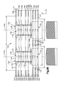
Referring initially to FIGS. 1A-2B, a PCB, for instance a PCB 100′ shown in FIG. 1A-B or a PCB 100″ shown in FIGS. 2A-B, can include one or more electrically conductive layers 102. In accordance with the illustrated embodiments, the PCB 100′ and the PCB 100″ each include nine conductive layers 102 a-i, although it will be understood that the PCB can include any number of conductive layers 102 as desired. The PCB 100′ and the PCB 100″ each define a top layer, for instance the electrically conductive layer 102 a, which can also be referred to as the top layer 102 a in accordance with illustrated embodiment. The PCB 100′ and the PCB 100″ each further define a bottom layer that is spaced from the top layer along a first or transverse direction T. In accordance with illustrated embodiments, the electrically conductive layer 102 i defines the bottom layer, and thus the electrically conductive layer can also be referred to as the bottom layer 102 i. Each of the electrically conductive layers 102 define a thickness TH as measured along the transverse direction T. The printed circuit boards (PCBs) 100′ and 100″ can each include a top surface 122 that supports the electrically conductive layer 102 a.
Various structures are described herein as extending vertically along the first or transverse direction “T” that is substantially perpendicular to a second or lateral direction “A” and a third or longitudinal direction “L”, and horizontally along the lateral direction A and the longitudinal direction L that is substantially perpendicular to the lateral direction A. As illustrated, the transverse direction “T” extends along an upward/downward direction of the PCBs 100′ and 100″. For instance, a direction from the top layer 102 a toward the bottom layer 102 i defines the downward direction, and a direction from the bottom layer 102 i to the top layer 102 a defines the upward direction. Thus, for instance, a first layer that is disposed in the upward direction from a second layer can be referred to as being above the second layer, and the second layer that is disposed in the downward direction from the first layer can be referred to as being below the first layer.
Thus, unless otherwise specified herein, the terms “lateral,” “longitudinal” and “transverse” are used to describe the orthogonal directional components of various components. It should be appreciated that while the longitudinal and lateral directions are illustrated as extending along a horizontal plane, and that while the transverse direction is illustrated as extending along a vertical plane, the planes that encompass the various directions may differ during use, depending, for instance, on the orientation of the various components. Accordingly, the directional terms “vertical” and “horizontal” are used to describe the PCBs and its components as illustrated merely for the purposes of clarity and convenience, it being appreciated that these orientations may change during use.
The PCBs 100′ and 100″ can further include one or more dielectric or electrically insulative layers 104, such as a plurality of dielectric layers or electrically insulative layers 104 a-h, that are disposed between the conductive layers 102 a-i along the transverse direction T. For instance, each dielectric layer 104 can be disposed between a select two conductive layers 102 to electrically isolate the select two conductive layers 102 from each other. Thus, the select two conductive layers 102 can be referred to as consecutive layers 102 because only one dielectric layer 104 is disposed between the consecutive layers 102 along the transverse direction T. A consecutive conductive layer 102 may be understood to be the next conductive layer 102 above or below a given conductive layer 102 along the transverse direction T. For instance, in accordance with the illustrated embodiment, conductive layers 102 b and 102 c can be referred to as consecutive conductive layers with respect to each other because only the dielectric layer 104 b is disposed between the conductive layers 102 b and 102 c along the transverse direction T.
The conductive layers 102 can include electrically conductive ground layers 106, electrically conductive signal layers 108, and electrically conductive power layers. In accordance with the illustrated embodiments, the conductive layers 102 a-b, 102 d-e, and 102 g-i are configured as electrically conductive ground layers 106 a-g, respectively. Further, in accordance with the illustrated embodiments, the conductive layers 102 c and 102 f are configured as electrically conductive signal layers 108 a-b, respectively. The signal layers 108 a-b can each include one or more conductive regions, such as electrically conductive traces 134 a-b, which can be made of copper or any other conductive material as desired. The conductive traces 134 a-b can each be part of a differential pair of signal traces 136. The ground layers 106 a-g can include one or more electrically conductive regions 107, which can be made of copper or any other electrically conductive material as desired. The dielectric layers 104 a-g can include dielectric or electrically nonconductive material, for instance plastic.
It will be appreciated that while FIGS. 1A-2B depict an example configuration of the PCB 100′ and the PCB 100″, the conductive layers 102 and the dielectric layers 104 can be arranged in a variety of sequences along the transverse direction T. Thus, the instant disclosure should not be limited to the example configuration shown in FIGS. 1A-2B.
Referring to FIGS. 1A-2B, the PCB 100′ and the PCB 100″ can each further include a plurality of signal vias 110, such as adjacent electrically conductive vias 110 a-b, which can also be referred to as electrically plated vias 110 a-b. In accordance with the illustrated embodiments, the electrically plated vias 110 a-b include a respective hole 112 a-b that defines a respective open end 114 a-b. Further, in accordance with the illustrated embodiment, the vias 110 a-b can extend into, for instance through, two or more of the conductive layers 102 and the dielectric layers 104 along the transverse direction T. The vias 110 a-b can further include a conductive surface 116. Each hole 112 a-b can be at least partially, for instance fully, plated with the conductive surface 116. Thus, the holes 112 a-b and the conductive surface 116 can be collectively referred to as plated, through-holes 118 a-b. The holes 112 a-b can be configured to be at least partially, for instance fully, filled with a conductive metal. The holes 112 a-b can receive an electrically conductive insert from another electronic device, such as a press fit connector for instance. In accordance with the illustrated embodiments, the vias 110 a-b can be electrically connected to electrically conductive surface pads, for instance a surface pad 120 that rests on the surface 122 of the PCB 100′ and 100″.
The vias 110 a-b are depicted in FIGS. 1A-2B as being cylindrical, although it will be appreciated that the vias can define any shape as desired. In accordance with the illustrated embodiment, each hole 112 a-b of the vias 110 a-b can define respective cross-sectional dimensions G and G′ along the lateral direction A or the longitudinal direction L. For instance, the holes 112 a-b, and thus the vias 110 a-b, can be cylindrical and thus the respective cross-sectional dimensions G and G′ can be diameters G and G′ that extend in a plane that is normal to the transverse direction T. Thus, each of the cross-sectional dimensions G and G′ can define a cross-sectional area of each via 110 a-b, respectively.
Still referring to FIGS. 1A-2B, traces 134 a-b of the signal layer 108 b are electrically coupled to the vias 110 a-b, respectively. Thus, the traces 134 in one or more of the signal layers 108 can be electrically coupled to one or more of the vias 110. In particular, the traces 134 a-b can be electrically coupled to the plated, through-holes 118 a-b, respectively, by contacting the conductive surfaces 116 of each of the plated, through-holes 118 a-b so as to establish an electrical connection between the traces 134 a-b and the vias 110 a-b. The vias 110 a-b can be connected to differential traces 134 a-b respectively, to establish a differential pair of signal traces.
With continuing reference to FIGS. 1A-2B, one or more of the conductive layers 102 can each include one or more electrically conductive regions 107 and one or more antipads 124 that are defined by respective electrically conductive regions 107. In accordance with the illustrated embodiments, the conductive layers 102 a-102 i include conductive regions 107 and antipads 124 a-r. Each of the antipads 124 can include a dielectric region 126 and a portion of a select electrically plated via 110 that extends through the dielectric region 126 along the transverse direction T. Thus, each of the antipads 124 can be referred to as an individual void in a respective conductive layer 102. Each antipad 124 can be surrounded by the conductive region 107 of each respective conductive layer 102. The antipads 124 may contain one or more of: a portion of one or more electrically conductive vias (such as vias 110 a-b), air, or a dielectric or electrically insulative material. In an example embodiment, individual antipads 124 may surround one or more of the vias 110, such as vias 110 a-b, and separate respective conductive regions 107 from the one or more vias 110 a-b, thereby preventing the conductive regions 107 from contacting an electrically conductive via 110. In accordance with the illustrated embodiments, the conductive layers 102 can include conductive regions 107 and dielectric regions 126 that electrically separate the conductive regions 107 from the electrically plated vias 110. In the electrically conductive ground layer 106 for instance, the dielectric regions 126 can be disposed between the conductive regions 107 and the conductive surfaces 116 of the vias 110 along the lateral and longitudinal directions A and L such that the conductive regions 107 and the vias 110 are electrically separate. The antipads 124 can each include a portion of the vias 110. For instance, the vias 110 can define a length along the transverse direction T, and the antipads 124 can each include a portion of the length of the vias 110 along the transverse direction T.
The antipads 124 can each have a cross-sectional area along a respective plane that is normal to the transverse direction T. For instance, a select antipad 124 of a select conductive layer 102 can have a maximum cross-sectional area along a select plane that is normal to the transverse direction T. The maximum cross-sectional area can be defined by a select conductive region 107 of the select conductive layer 102, wherein the dielectric region 126 of the select antipad 124 is aligned with the select conductive region 107 along the select plane. Further, each antipad 124 can have a maximum volume which can be defined by a product of the maximum area and the thickness TH of the respective conductive layer 102.
The antipads 124 may be formed in a variety of ways. For example, each of antipads 124 a-i may be created by first forming conductive regions 107 of the respective conductive layers 102 a-i and then removing sections of the conductive regions 107 to create the respective dielectric regions 126 through, for example, etching. As will be explained further below, select ones of the antipads 124 may also be formed by back drilling.
Referring still to FIGS. 1A-2B, the PCB 100′ includes antipads 124 a-e that are above the antipads 124 g-l along the transverse direction T, and the PCB 100″ includes antipads 124 a-f that are above the antipads 124 m-r along the transverse direction T. In accordance with the illustrated embodiments, the antipads 124 a-e are depicted as being rectangular although it will be appreciated that the antipads 124 a-e can assume a wide variety of shapes as desired. As illustrated, the antipads 124 a-e can define a first cross-sectional dimension X defined by a longest straight line that extends from an edge of the conductive region 107 to an opposed edge of the conductive region 107 along the lateral direction X. Further, with particular reference to FIGS. 1B, 2B, 3B and 4B, the antipads 124 a-e can define a second cross-sectional dimension B defined by a longest straight line that extends from an edge of the conductive region 107 to an opposed edge of the conductive region 107 along the longitudinal direction L. Thus, a maximum cross-sectional area, which can be referred to as a maximum area, of the antipads 124 a-e along a respective plane that is normal to the transverse direction T can be substantially equal to a product of the first cross-sectional dimension A and the second cross-sectional dimension B. Further, the maximum cross-sectional area of the antipads 124 a-e can be rectangular, and each of the antipads 124 a-e can have a maximum volume that can be defined by a product of the respective maximum cross-sectional area and the thickness TH of the respective conductive layer 102. Select ones of the antipads 124, for instance the illustrated antipads 124 a-e, can include portions of more than one via 110, for instance two vias 110 a-b in accordance with the illustrated embodiments. Thus, the maximum cross-sectional areas of the antipads 124 a-e along respective planes that are normal to the transverse direction T can be larger than maximum cross-sectional areas of the vias 110 a-b along respective planes that are normal to the transverse direction T.
With particular reference to FIGS. 1A-B, the PCB 100′ can include conductive layers 102 g-i that include the antipads 124 g-l. For instance, in accordance with the illustrated embodiment, the conductive layer 102 g includes the antipads 124 g and 124 j spaced from each other along the longitudinal direction L, the conductive layer 102 h includes the antipads 124 h and 124 k spaced from each other along the longitudinal direction L, and the conductive layer 102 i includes the antipads 124 i and 124 l spaced from each other along the longitudinal direction L. It will be understood that the conductive layers 102 can include any number of antipads 124 as desired and the antipads 124 can be positioned on the respective conductive layers as desired. The antipads 124 g-l are depicted as being cylindrical although it will be appreciated that the antipads 124 g-l can assume a wide variety of shapes as desired. As illustrated, the antipads 124 g-i can define a cross-sectional dimension C defined by a longest straight line that extends from an edge of the conductive region 107 to an opposed edge of the conductive region 107 along the lateral direction A. The cross-sectional dimension C can be a diameter C, and thus the cross-sectional dimension C can also be defined by a longest straight line that extends from an edge of the conductive region 107 to an opposed edge of the conductive region along the longitudinal direction L. Similarly, as illustrated, the antipads 124 j-l can define a cross-sectional dimension C′ defined by a longest straight line that extends from an edge of the conductive region 107 to an opposed edge of the conductive region 107 along the longitudinal direction L. The cross-sectional dimension C′ can be a cross-sectional diameter C′, and thus the cross-sectional dimension C′ of the antipads 124 j-l can also be defined by a longest straight line that extends from an edge of the conductive region 107 to an opposed edge of the conductive region along the lateral direction A.
With continuing reference to FIGS. 1A-B, the antipads 124 g-i and 124 j-l can have maximum cross-sectional areas, which can be referred to as maximum area, along respective planes that are normal to the transverse direction T, and the maximum cross sectional areas of the antipads 124 g-i and 124 j-l can be defined by the cross-sectional dimensions, for instance cross-sectional diameters, C and C′, respectively. In accordance with the illustrated embodiment, the maximum cross-sectional areas of each of the antipads 124 g-l can be less than the maximum cross-sectional areas of each of the antipads 124 a-e. Thus, the cross-sectional dimensions C and C′ of the antipads 124 g-i and 124 j-l, respectively, can be less than one or both of the cross-sectional dimensions X and B of the antipads 124 a-e. Further, the maximum cross-sectional areas of each of the antipads (e.g., antipads 124 g-l) below the signal layer 108 can be circular, or otherwise shaped differently than the antipads 124 a-e that are disposed above the signal layer 108 along the transverse direction T. Each antipad 124 g-l can have a maximum volume that can be defined by a product of the respective maximum cross-sectional area and the thickness TH of the respective conductive layer 102. Select ones of the antipads 124, for instance the illustrated antipads 124 g-l, can include portions of only one via 110. For instance, in accordance with the illustrated embodiment, the antipads 124 g-i include a portion of only the via 110 a and the antipads 124 j-l include a portion of only the via 110 b. The antipads 124 g-l can further include dielectric regions 126 that separate the vias 110 from the conductive regions 107 along respective planes that are normal to the transverse direction T. Thus, the maximum cross-sectional areas of the antipads 124 g-l along respective planes that are normal to the transverse direction T can be larger than maximum cross-section areas of the vias 110 a-b along respective planes that are normal to the transverse direction T. For instance, the maximum cross-sectional areas of the antipads 124 g-l can include dielectric regions 126 that electrically separate the conductive regions 107 from the electrically plated vias 110.
Thus, the PCB 100′ can include a first electrically conductive layer, for instance a select one of the conductive layers 102 a-e, that includes a first conductive region, for instance the conductive region 107, and a first antipad, for instance a select one of the antipads 124 a-e. The first antipad can include a first dielectric region, for instance the dielectric region 126, and a portion of a first electrically plated via, for instance the via 110 a, that extends through the first dielectric region along the transverse direction T. The first antipad can have a first maximum area along a first plane that is normal to the transverse direction T, and the first dielectric region can be aligned with the first electrically conductive region along the first plane. The PCB 100′ can further include a first dielectric layer, for instance a select one of the dielectric layers 104 a-f, that is disposed below the first electrically conductive layer along the transverse direction T. The PCB 100′ can further include a second electrically conductive layer, for instance a select one of the conductive layers 102 g-i, that is disposed below the first dielectric layer along the transverse direction T. The second electrically conductive layer can include a second electrically conductive region and a second antipad, for instance a select one of the antipads 124 g-i, defined by the second electrically conductive region. The second antipad can have a second maximum area along a second plane that is normal to the transverse direction T, and the second maximum area can be less than the first maximum area.
Further, the PCB 100′ can include a third electrically conductive layer, for instance a select one of the electrically conductive layers 102 h and 102 i, that is disposed below the second electrically conductive layer along the transverse direction T such that that no additional electrically conductive layer is disposed between the second electrically conductive layer and the third electrically conductive layer along the transverse direction T. The third electrically conductive layer can define a third electrically conductive region and a third antipad, for instance a select one of the antipads 124 h and 124 i, defined by the third electrically conductive region. The third antipad can have a third maximum area along a third plane that is normal to the transverse direction T. The third maximum area can be substantially equal to the second maximum area. As used herein, two or more values that are substantially equal to each other may refer to values that are within tolerances of a manufacturer. At least a portion of each of the second antipad and the third antipad can be aligned with the portion of the first electrically plated via along the transverse direction T.
The first antipad can further include a portion of a second electrically plated via, for instance the via 110 b, that extends through the first dielectric region along the transverse direction T. Further, the second electrically conductive layer can include a fourth antipad, for instance a select one of the antipads 124 j-l, that has a fourth maximum area along the second plane. The fourth maximum area can be substantially equal to the second maximum area. The third electrically conductive layer can further include a fifth antipad, for instance a select one of the antipads 124 k and 124 l, that is defined by the third electrically conductive region. The fifth antipad can have a maximum area along the third plane. The fifth maximum area can be substantially equal to the third maximum area.
The PCB 100′ can further include a second dielectric layer disposed between the second electrically conductive layer and the third electrically conductive layer such that the second dielectric layer separates the second and third electrically conductive layers from each other and the second dielectric layer abuts each of the second and third electrically conductive layers.
Referring now to FIGS. 2A-B, the PCB 100″ can include conductive layers 102 g-i that include the antipads 124 m-r. For instance, in accordance with the illustrated embodiment, the conductive layer 102 g includes the antipads 124 m and 124 p spaced from each other along the longitudinal direction L, the conductive layer 102 h includes the antipads 124 n and 124 q spaced from each other along the longitudinal direction L, and the conductive layer 102 i includes the antipads 124 o and 124 r spaced from each other along the longitudinal direction L. The antipads 124 m-r are depicted as being cylindrical although it will be appreciated that the antipads 124 m-r can assume a wide variety of shapes as desired. As illustrated, the antipads 124 m-o can define a cross-sectional dimension F defined by a longest straight line that extends from an edge of the conductive region 107 to an opposed edge of the conductive region 107 along the lateral direction A. The cross-section dimension F can be a diameter F, and thus the cross-sectional dimension F can also be defined by a longest straight line that extends from an edge of the conductive region 107 to an opposed edge of the conductive region along the longitudinal direction L. Similarly, as illustrated, the antipads 124 p-r can define a cross-sectional dimension F′ defined by a longest straight line that extends from an edge of the conductive region 107 to an opposed edge of the conductive region 107 along the longitudinal direction L. The cross-sectional dimension F′ can be a cross-sectional diameter F′, and thus the cross-sectional dimension F′ of the antipads 124 p-r can also be defined by a longest straight line that extends from an edge of the conductive region 107 to an opposed edge of the conductive region along the lateral direction A.
With continuing reference to FIGS. 2A-B, the antipads 124 m-o and 124 p-r can have maximum cross-sectional areas, which can be referred to as maximum areas, along respective planes that are normal to the transverse direction T, and the maximum cross-sectional areas of the antipads 124 m-o and 124 p-r can be defined by the cross-sectional dimensions, for instance cross-sectional diameters, F and F′, respectively. In accordance with the illustrated embodiment, the maximum cross-sectional areas of each of the antipads 124 m-r can be less than the maximum cross-sectional areas of each of the antipads 124 a-e. Further, the maximum cross-sectional areas of the antipads 124 m-r below the signal layer 108 can be circular, or otherwise shaped differently than the antipads 124 a-e that are disposed above the signal layer 108 along the transverse direction T. Thus, the cross-sectional dimensions F and F′ of the antipads 124 m-o and 124 p-r, respectively, can be less than one or both of the cross-sectional dimensions X and B of the antipads 124 a-e. In accordance with the illustrated embodiment, for instance before back drilling of the vias 110 a-b, the cross-section dimensions F and F′ can be substantially equal, for instance slightly larger, to the cross-sectional dimensions G and G′, respectively. Thus, before back drilling for instance, the maximum cross-section areas of the antipads 124 m-r along respective planes that are normal to the transverse direction T can be substantially equal to the maximum cross-section areas of the vias 110 a-b along respective planes that are normal to the transverse direction T. Before back drilling described below, the conductive regions 107 of the conductive layers 102 g-i can be electrically coupled to the electrically conductive vias 110 a-b, as illustrated.
In another example in which the antipads 124 m-r have the cross-sectional dimensions F and F′ that are slightly larger than the cross-sectional diameters G and G′, respectively, the conductive regions 107 of the conductive layers 102 g-i are not electrically coupled to the electrically conductive vias 110 a-b. Thus, the maximum cross-section area of antipads 124 m-r can include a dielectric or electrically insulative material, such as the dielectric region 126, that electrically separates the vias 110 a-b from the conductive regions 107 of the conductive layers 102 g-i.
Referring to FIGS. 1A-2B, the vias 110 a-b can include an unused portion 128, which can be referred to as a resonant stub. The unused portion 128 may be located above or below the signal layer 108 along the transverse direction T. In accordance with the illustrated embodiments, the unused portion 128 is disposed below the signal layers 108 along the transverse direction T. The unused portion 128 of the vias 110 a-b can be located below the signal layer 108 b in the conductive layers 102 g-i. The unused portion 128 of the vias 110 a-b can be disposed in a first group of conductive layers 102 having antipads 124 that are smaller than antipads in a second group of conductive layers 102. For example, the first group may include the consecutive conductive layers 102 g-i that are disposed below the signal layer 108 along the transverse direction T, and the second group may include consecutive conductive layers 102 a-e that are disposed above the signal layer 108 along the transverse direction T. The first group of conductive layers 102 g-i may be disposed on a side of signal layer 108 b opposite the second group of conductive layers 102 a-e along the transverse direction T. For example, the first group of conductive layers 102 g-i may be above or below the second group of conductive layers 102 a-e along the transverse direction T. The antipads 124 g-r of the first group of conductive layers 102 may be smaller than the antipads 124 a-e contained in the second group.
The unused portion 128 of the vias 110 a-b can act as a notch filter centered around a frequency that is primarily determined by a length of the unused portion 128. The length of the unused portion 128 can be measured along the transverse direction T. The unused portion 128 can cause some of the energy of an electrical signal that is transitioning through the plated, through-hole 118 along the transverse direction T to be reflected back to the source. To mitigate this interference, the unused portions 128 of each respective via 110 a-b can be removed. Referring to FIGS. 3A-4B, the unused portion 128 can be removed using, for example, a circular drill bit with a diameter H attached to a drill.
Referring to FIGS. 3A-4B, the drill may be used to back drill the PCB 100. For instance, the drill may be inserted along the upward direction to a depth such that most, for instance all, of the unused portion 128 of each respective via 110 a-b is removed. For example, when inserted along the upward direction, the drill may be stopped at a location below the signal layer 108. Referring to FIGS. 2A-B and 4A-B, the drill may also remove a portion of each of the conductive regions 107 of the conductive layers 102 g-i. Referring also to FIGS. 1A-B and 3A-B, the drill may also remove a portion of each of the antipads 124 g-l of the conductive layers 102 g-i.
Referring again to FIGS. 3A-4B, the PCB 100′ and the PCB 100″ can include a single back drilled cavity 130 that can be created as result of the back drilling described above. The cavity 130 can have a circular cross section as viewed along the transverse direction. The circular cross section of the cavity 130 can define a diameter H that is substantially equal to the diameter H of the drill bit. During the back drilling process, a part of the unused portions 128 of each of the vias 110 a-b and portions of each of the conductive layers 102 g-i may be removed. In order to avoid damaging the traces 134 a-b in the signal layer 108 b, a small section of the unused portion 128 may remain in the dielectric or electrically insulative layer 104 f that is disposed between the conductive layers 102 f and 102 g along the transverse direction T. Referring to FIGS. 2A and 4A, enough of the unused portion 128 may be removed such that the conductive regions 107 of the conductive layers 102 g-i are not electrically connected to either of the vias 110 a-b. After back drilling, in accordance with an example embodiment, at least a portion, for instance all, of the cavity 130 can be filled, for instance back-filled, with a dielectric material, for instance a dielectric material other than air. The cavity 130 can be filled with the same dielectric material that is included in the dielectric layers 104, such as a plastic or an epoxy for example.
In accordance with the illustrated embodiments, the cavity 130 can be located below the signal layer 108 b along the downward direction that extends from the layer 102 a toward the layer 102 i. For example, the cavity 130 may extend between the dielectric or electrically insulative layer 104 f and the conductive layer 102 i along the transverse direction T. The cavity 130 any be consist of any dielectric or electrically insulative material, for instance air, as desired. For instance, after the cavity 130 is back-drilled, the cavity can be at least partially filled with a dielectric material other than air.
Thus, in accordance with the an example embodiment, a printed circuit board can include a first electrically conductive layer that includes a first electrically conductive region and a first antipad defined by the first electrically conductive region. The first antipad can include a first dielectric region and a portion of an electrically plated via that extends through the first dielectric region along a first direction. The first dielectric layer can be disposed below the first electrically conductive layer along the first direction. The printed circuit board can further include a second electrically conductive layer disposed below the first dielectric layer along the first direction. The second electrically conductive layer can include at least a portion of a back-drilled cavity that is aligned with the portion of the electrically plated via along the first direction. Further, the back-drilled cavity can be at least partially filled with a dielectric material other than air.
With particular reference to FIGS. 3A-B, after the unused portions 128 of the vias 110 a-b are removed and the cavity 130 is created, in accordance with the illustrated embodiment, the cross-sectional dimensions C and C′ of the antipads 124 g-l can be larger than the diameter H of the cavity 130. Thus, the size of the antipads 124 g-l may remain unchanged after back drilling. Further, select conductive regions 107, for instance the second and third electrically conductive regions, of the conductive layers 102 g-i do not come into contact with the single back drilled cavity 130 in accordance with the illustrated embodiment shown in FIGS. 3A-B. After back drilling, each of the antipads 124 g-l can include respective portions of the cavity 130, for instance instead of the vias 110 a-b. Referring to FIGS. 3A-B, after back drilling, the antipads 124 g-l can include respective portions of the dielectric region 126 and respective portions of the cavity 130. Stated another way, the diameter H of the drill bit used to remove the unused portion 128 may be smaller than the cross-sectional dimensions C and C′ of the antipads 124 g-l. In an example embodiment, the cross-sectional dimensions C and C′ of the antipads 124 g-l may be predetermined to be slightly greater than the diameter H of the drill used to remove the unused portions 128. Thus, the second antipad, for instance a select one of the antipads 124 g-r, and a third antipad, for instance a select one of the antipads 124 h-i, 124 k-l, 124 n-o, and 124 q-r, can be least partially defined by the single back drilled cavity 130 that extends at least from the second antipad to the third antipad along the transverse direction T.
Referring to FIGS. 4A-B, the diameter H of the drill may be larger than the cross-section dimensions F and F′ of the antipads 124 m-r. Thus, when the unused portions 128 of vias 110 a-b are removed, the section of the conductive layers 102 g-i and the dielectric layers 104 f-h can be removed to create the cavity 130 having the diameter H. Due to back drilling the PCB 100″, for instance, the antipads 124 m-r can have the cross-sectional dimension H that is measured from opposed sides of the cavity 130 along a direction that is perpendicular to the transverse direction T, and antipads 124 m-r can have the cross-section dimension H that is increased from the cross-section dimensions F and F′. Thus, the maximum area of the antipads 124 m-r along respective planes that are normal to the transverse direction T can also be increased by back drilling the PCB 100″. By removing the unused portion 128 and the section of conductive layers 102 g-i, in particular sections of the conductive regions 107 of the conductive layers 102 g-i, the conductive regions 107 of the conductive layers 102 g-i are electrically separate from the vias 110 a-b. Further, select conductive regions 107, for instance the second and third electrically conductive regions, of the conductive layers 102 g-i come into contact with the single back drilled cavity 130 in accordance with the illustrated embodiment shown in FIGS. 4A-B.
Referring to FIGS. 3A-B, a select two conductive regions, for instance the conductive regions 107 of the conductive layers 102 g-i, do not come into contact with the single back drilled cavity 130. Alternatively, referring to FIGS. 4A-B, another select two conductive regions, for instance the conductive regions 107 of conductive layers 102 g-i of FIG. 4A, come into contact with the back drilled cavity 130.
Referring generally to FIGS. 1A-4B, the vias 110 a-b may be elongate along the transverse direction T and the vias 110 a-b can be cylindrical. In accordance with the illustrated embodiments, the via 110 a can be centered around a first center line 132 a that extends along the transverse direction T, and the via 110 b can be centered around a second centerline 132 b that extends along the transverse direction T. For instance, the vias 110 a-b can define respective cylinders that define the centerlines 132 a-b. In accordance with the illustrated embodiment, the centerline 132 a can extend through respective centers of select antipads 124, for instance the second and the third antipads, and the centerline 132 b can extend through respective centers of select antipads 124, for instance the fourth and the fifth antipads, along the transverse direction T. At least a portion, for instance all, of the antipads 124 g-r can be aligned with the respective vias 110 a-b such that the respective centerlines 132 pass through the antipads 124 g-r along the transverse direction T. For instance, the antipads 124 g-i and 124 m-o can be aligned with the via 110 a along the transverse direction T such the center line 132 passes through a respective center of the antipads 124 g-i and 124 m-o along the transverse direction T. Similarly, the antipads 124 j-l and 124 p-r can be aligned with the via 110 b along the transverse direction T such that the center line 132 b passes through a respective center of the antipads 124 j-l and 124 p-r along the transverse direction T. In accordance with the illustrated embodiments, when the unused portions 128 of the vias 110 a-b are removed by back drilling, the drill bit may be inserted along the center lines 132 a-b along the transverse direction, which can result in at least a portion, for instance all, of the cavities 130 being aligned with the vias 110 a-b along the transverse direction T. For instance, the cavity 130 can be aligned with the respective vias 110 a-b such that the respective center line 132 a-b passes through a respective center of the cavity 130 along the transverse direction T.
Without being bound by theory, by minimizing the size of the antipads 124 g-r, as depicted in FIGS. 3A-4B, the amount of layer-to-layer cross talk can be reduced. Further, the layer-to-layer cross talk can be reduced by the antipads 124 g-r assuming cylindrical shapes with circular cross-sectional areas along respective planes that are normal to the transverse direction T, while the antipads 124 a-e can be rectangular shaped.
Referring to FIGS. 5A-B, a PCB 200 can include at least three planar conductive layers 202 such as electrically conductive layers 202 a-c. In accordance with the illustrated embodiment, the planar conductive layers 202 a-c can each define a thickness in the transverse direction T. The conductive layers 202 a-c can be spaced from each other along the transverse direction T. For instance, in accordance with the illustrated embodiment, the conductive layer 202 b is in between the conductive layers 202 a and 202 c along the transverse direction T, and the conductive layers 202 a and 202 c can be referred to as a top layer 202 a and a bottom layer 202 c, respectively. Because no other conductive layer is placed between the conductive layers 202 a-c along the transverse direction T, the conductive layers 202 a-c may also be referred to as consecutive conductive layers 202 a-c. The conductive layer 202 b can be configured as a ground layer 206 b and the conductive layers 202 a and 202 c can be configured as signal layers 206 a and 206 c, respectively. Thus, the conductive layer 202 b can include conductive regions 207 and one more antipads 210. The conductive layers can also be configured as power layers as desired.
The signal layers 206 a and 206 c can each include one or more conductive traces 208. In accordance with the illustrated embodiment, the signal layer 206 a includes a first differential pair 208 a of electrical signal traces, and the signal layer 206 c includes a second differential pair 208 b of electrical signal traces. Each of the differential pairs 208 a-b of signal traces includes two conductive traces 208 that are elongate in the longitudinal direction L and spaced from each other along the lateral direction A. The conductive traces 208 can be made of copper or any other electrically conductive material as desired. The first differential pair 208 a of electrical signal traces can define a first centerline 216 a centrally disposed between the electrical signal traces 208 of the first differential signal pair 208 a. The second differential pair 208 b of electrical signal traces can define a second centerline 216 b centrally disposed between the electrical signal traces 208 of the second differential signal pair 208 b.
The PCB 200 can further include one or more dielectric or electrically insulative layers 204, for instance dielectric layers 204 a-b, that are located between the conductive layers 202 a-c along the transverse direction T. In accordance with the illustrated embodiment, the dielectric layer 204 a is located between the signal layer 206 a and the ground layer 206 b along the transverse direction T, and the dielectric layer 204 b is located between the signal layer 206 c and the ground layer 206 b along the transverse direction T. The ground layer 206 b may include the conductive region 207 that consists of conductive material such as copper. The dielectric layers 204 a-b may include substrate material such as plastic.
The PCB 200, and in particular the electrically conductive layer 202 b, may further include antipads 210 arranged in a first row R1 along the longitudinal direction L. The PCB 200 may further include antipads 210 arranged in a second row R2 along that longitudinal direction L. The first row R1 can be spaced from the second row R2 a second distance D2 along the lateral direction A. In accordance with the illustrated embodiment, the antipads 210 can define a rectangular shape, although it will be understood that the antipads can be alternatively shaped as desired. The PCB 200 can further include ground vias 212 that are disposed between antipads 210 along the longitudinal direction L. For instance, in accordance with the illustrated embodiment, one ground via is disposed between each pair of adjacent antipads 210 along the row R1 and one ground via is disposed between each pair of adjacent antipads 210 along the row R2, although it will be understood that any number of ground vias can be alternatively located as desired. While not shown in FIGS. 5A and 5B, the antipads 210 can include one or more signal vias.
With continuing reference to FIGS. 5A-B, the differential signal pair 208 a can define an edge 214 a that is proximate to the first row R1 along the lateral direction A. For instance, the edge 214 a can be a third distance D3 from a select one of the antipads 210 in the first row R1 as measured in a straight line along the lateral direction A. The differential signal pair 208 a can further define an edge 215 a that is opposite the edge 214 a and that is proximate to the second row R2 along the lateral direction A. The edge 215 a that is opposite the edge 214 a can be a fourth distance from a select one of the antipads 210 in the second row R2 as measured in a straight line along the lateral direction A. The edge 214 a can be spaced from the opposed edge 215 a a first distance D1 a. The sum of the third distance D3, the first distance D1 a, and the fourth distance D4 may equal the second distance D2.
The differential signal pair 208 b can define an edge 214 b that is proximate to the first row R1 along the lateral direction A. For instance, the edge 214 b can be a fifth distance D5 from a select one of the antipads 210 in the first row R1 as measured in a straight line along the lateral direction A. The differential signal pair 208 b can further define an edge 215 b that is opposite the edge 214 b and that is proximate to the second row R2 along the lateral direction A. The edge 215 b that is opposite the edge 214 b can be a sixth distance D6 from a select one of the antipads 210 in the second row R2 as measured in a straight line along the lateral direction A. The edge 214 b can be spaced from the opposed edge 215 b a first distance D1 b that can be substantially equal to the first distance D1 a. Thus, the electrical signal traces 208 of the first differential pair 208 a of signal traces can be spaced apart from each other a first distance D1 a along the second or lateral direction A, wherein the first distance can be substantially equal to a distance that the electrical signal traces 208 in the second differential pair 208 b of signal traces are spaced apart from each other in the lateral direction A. The sum of the fifth distance D5, the first distance D1 b, and the sixth distance D6 can equal the second distance D2.
In accordance with the illustrated embodiment, the third distance D3 may be substantially equal to the sixth distance D6. Thus, the PCB 200 can include the electrically conductive layer 202 b disposed between the first differential signal pair 208 a and the second differential signal pair 208 b along the transverse direction T, and the electrically conductive layer 202 b can further include the electrically conductive region 207 and one more antipads 210, for instance first and second antipads 210, that are defined by the electrically conductive region 207. For instance, the first antipad 210 can be disposed in the first row R1 and the second antipad 210 can be disposed in the second row R2. Thus, the first and second antipads 210 can be spaced from each other along the lateral direction A that is perpendicular to the transverse direction T. In accordance with the illustrated embodiment, each of the first and second differential pairs 208 a and 208 b can be disposed between the first and second antipads 210 with respect to the lateral direction A. Further, in accordance with the illustrated embodiment, the first centerline 216 a can be disposed closer to the first antipad 210 than the second antipad 210 along the lateral direction A, and the second centerline 216 b can disposed closer to the second antipad 210 than the first antipad 210 along the lateral direction A. Thus, the fourth distance D4 can be greater than the sixth distance D6. Further, the fifth distance D5 can be greater than the third distance D3.
With continuing reference to FIGS. 5A-B, a portion of the first differential pair 208 a of electrical signal traces can be aligned with a portion of the second differential pair 208 b of electrical signal traces along the transverse direction T. For instance, the fourth distance D4 may be substantially equal to the fifth distance D5 such that a portion of the first differential pair 208 is aligned with a portion of the second differential pair 208 b along the transverse direction T. Similarly, the third distance D3 can be substantially equal to the sixth distance D6 such that a portion of the first differential pair 208 is aligned with a portion of the second differential pair 208 b along the transverse direction T. For instance, portions of the differential signal pairs 208 a-b can aligned along the transverse direction T such that a distance between the edge 215 a and the edge 214 b is less than the first distances D1 a and D1 b.
The first centerline 216 a can be disposed closer to the antipads 210 in the first row R1 than the antipads 210 in the second row R2, and the second centerline 216 b can be disposed closer to the antipads 210 in the second row R2 than the antipads 210 in the first row R2 by selecting appropriate values for the distances D3, D4, D5, and D6. For example, as depicted in FIG. 5B, the distance D3 is less than the distance D5 and the distance D4 is greater than the distance D6, which can result in the edges 214 a and 214 b being offset (spaced) from one another along the lateral direction A. While FIG. 5B depicts one example, it should be appreciated that a wide variety of values can be assigned to the distances D3, D4, D5, and D6 to result in the first centerline 216 a being disposed closer to the first row R1 than the second row R2 along the lateral direction A, and the second centerline 216 b being disposed closer to the second row R2 than the first row R1 along the lateral direction A.
Without being bound by theory, by spacing the centerlines 216 a and 216 b with respect to each other along the lateral direction A, it may be possible to reduce electromagnetic interference, such as cross talk, between the signal pairs 208 a and 208 b. This may be accomplished by preventing or reducing the alignment of the magnetic field of the signal pair 208 a with the magnetic field of the signal pair 208 b. Additionally, as magnetic fields are circular, the magnetic wave generated by, for example, the edge 214 a would have to travel in a large circular path in order to reach the edge 215 a. This may increase the electrical distance magnetic waves would have to travel, thus making those waves reaching the edge 215 weaker. Further, the larger the circular path becomes, the higher the likelihood magnetic waves impact another ground layer, which may be disposed below the signal pair 208 a along the transverse direction T, and become absorbed. The above also applies to the magnetic waves from the signal pair 208 b to the signal pair 208 a
In accordance with one embodiment, a method can be provided for reducing layer-to-layer crosstalk. The method can include the step of providing or teaching the use of a PCB, such as either of PCB 100′ or PCB 100″ as described in connection with FIGS. 1A-2B. The method may further include the teaching the step of back drilling, as described above in connection with FIGS. 3A through 4B, the PCB along an upward direction so as to remove at least a portion of the electrically conductive material. The method may further include selling to the third party the printed circuit board.
In accordance with one embodiment, a method can be provided for reducing layer-to-layer crosstalk. The method can include the step of providing or teaching to a third party the use of a PCB board comprising a first electrically conductive layer that includes a first electrically conductive region and a first antipad defined by the first electrically conductive region, the first antipad including a first dielectric region and a portion of a first electrically plated via that extends through the first dielectric region along a first direction, the first antipad having a first maximum area along a first plane that is normal to the first direction, wherein the first dielectric region is aligned with the first electrically conductive region along the first plane. The method can further include the step of providing or teaching to a third party the use of the PCB board that further includes a second electrically conductive layer disposed below the first dielectric layer along the first direction, the second electrically conductive layer including a second electrically conductive region and a second antipad defined by the second electrically conductive region, the second antipad having a second maximum area along a second plane that is normal to the first direction, the second maximum area less than the first maximum area. The method may further include teaching the step to the third party of applying a first differential pair of electrical signal traces and a second differential pair of electrical signal traces to opposed sides of an electrically conductive ground layer, wherein the first differential pair of electrical signal traces is disposed closer to the first antipad than the second antipad along a second direction that is perpendicular to the first direction, wherein the second differential pair of electrical signal traces is disposed closer to the second antipad than the first antipad along the second direction, and wherein each of the first and second differential pairs is disposed between the first and second antipads. The method may also include selling the PCB board to the third party or purchasing the PCB board, which may include the first and the second differential pairs of signal traces, from the third party.
The embodiments described in connection with the illustrated embodiments have been presented by way of illustration, and the present invention is therefore not intended to be limited to the disclosed embodiments. Furthermore, the structure and features of each of the embodiments described above can be applied to the other embodiments described herein, unless otherwise indicated. Accordingly, the invention is intended to encompass all modifications and alternative arrangements included within the spirit and scope of the invention, for instance as set forth by the appended claims.

Claims (25)

What is claimed:
1. A printed circuit board comprising:
a first electrically conductive layer that includes a first electrically conductive region and a first antipad defined by the first electrically conductive region, the first antipad including a first dielectric region and a portion of a first electrically plated via that extends through the first dielectric region along a first direction, the first antipad having a first maximum area along a first plane that is normal to the first direction, wherein the first dielectric region is aligned with the first electrically conductive region along the first plane;
a first dielectric layer disposed below the first electrically conductive layer along the first direction;
a second electrically conductive layer disposed below the first dielectric layer along the first direction, the second electrically conductive layer including a second electrically conductive region and a second antipad defined by the second electrically conductive region, the second antipad having a second maximum area along a second plane that is normal to the first direction, the second maximum area less than the first maximum area;
a third electrically conductive layer disposed below the second electrically conductive layer along the first direction such that no additional electrically conductive layer is disposed between the second electrically conductive layer and the third electrically conductive layer along the first direction, the third electrically conductive layer defining a third electrically conductive region and a third antipad, the third antipad having a third maximum area along a third plane that is normal to the first direction, the third maximum area substantially equal to the second maximum area; and
an electrically conductive signal layer that includes one or more electrically conductive traces electrically coupled to the first electrically plated via, the electrically conductive signal layer being the only signal layer disposed between the first electrically conductive layer and the second electrically conductive layer along the first direction,
wherein at least a portion of each of the second antipad and the third antipad is aligned with the portion of the first electrically plated via along the first direction.
2. The printed circuit board of claim 1, wherein the first antipad further includes a portion of a second electrically plated via that extends through the first dielectric region along the first direction,
wherein the second electrically conductive layer further includes a fourth antipad defined by the second electrically conductive region, the fourth antipad having a fourth maximum area along the second plane, the fourth maximum area substantially equal to the second maximum area,
wherein the third electrically conductive layer further includes a fifth antipad defined by the third electrically conductive region, the fifth antipad having a fifth maximum area along the third plane, the fifth maximum area substantially equal to the third maximum area.
3. The printed circuit board of claim 1, wherein each of the second antipad and the third antipad are at least partially defined by a single back drilled cavity that extends at least from the second antipad to the third antipad along the first direction.
4. The printed circuit board of claim 3, wherein each of the second electrically conductive region and the third electrically conductive region do not come into contact with the single back drilled cavity.
5. The printed circuit board of claim 3, wherein at least one of the second electrically conductive region and the third electrically conductive region comes into contact with the single back drilled cavity.
6. The printed circuit board of claim 3, wherein the single back drilled cavity is at least partially filled with a dielectric medium.
7. A printed circuit board comprising:
a first signal layer comprising a first differential pair of electrical signal traces that defines a first centerline oriented along a transverse direction, wherein the first centerline is centrally disposed between the electrical signal traces of the first differential signal pair with respect to a lateral direction;
a second signal layer comprising a second differential pair of electrical signal traces spaced from the first differential pair along the transverse direction, the second differential pair defining a second centerline centrally oriented along the transverse direction, wherein the second centerline is disposed between the electrical signal traces of the second differential signal pair with respect to the lateral direction; and
an electrically conductive layer disposed between the first differential signal pair and the second differential signal pair with respect to the transverse direction, wherein the first centerline and the second centerline are offset with respect to each other along the lateral direction to reduce electromagnetic interference between the first differential signal pair and the second differential signal pair,
wherein the first differential pair of electrical signal traces defines the first centerline such that the first centerline is centrally disposed between no differential pairs of electrical signal traces of the second signal layer.
8. The printed circuit board of claim 1, further comprising:
a second dielectric layer disposed between the second electrically conductive layer and the third electrically conductive layer such that the second dielectric layer separates the second and third electrically conductive layers from each other and the second dielectric layer abuts each of the second and third electrically conductive layers.
9. The printed circuit board of claim 1, wherein the second and third maximum areas are circular.
10. The printed circuit board of claim 9, wherein the first maximum area is rectangular.
11. The printed circuit board of claim 1, wherein the first, second, and third electrically conductive layers are ground layers.
12. The printed circuit board of claim 1, wherein the first electrically plated via defines a cylinder defining a centerline that extends through respective centers of the second antipad and the third antipad along the first direction.
13. The printed circuit board of claim 2, wherein the second electrically plated via defines a cylinder defining a centerline that extends though respective centers of the fourth antipad and the fifth antipad along the first direction.
14. The printed circuit board of claim 3, wherein the first electrically plated via defines a cylinder defining a centerline that passes through a respective center of the single back drilled cavity along the first direction.
15. A printed circuit board comprising:
a first differential pair of electrical signal traces that defines a first centerline centrally disposed between the electrical signal traces of the first differential signal pair;
a second differential pair of electrical signal traces spaced from the first differential pair along a first direction, the second differential pair defining a second centerline centrally disposed between the electrical signal traces of the second differential signal pair; and
an electrically conductive layer disposed between the first differential signal pair and the second differential signal pair along the first direction, the electrically conductive layer including an electrically conductive region and first and second antipads that are defined by the electrically conductive region, the first and second antipads spaced from each other along a second direction that is perpendicular to the first direction, wherein each of the first and second differential pairs is disposed between the first and second antipads with respect to the second direction; and
at least one ground via spaced from each of the first and second antipads along a third direction that is substantially perpendicular to both the first and second directions,
wherein the first centerline is disposed closer to the first antipad than the second antipad along the second direction, and the second centerline is disposed closer to the second antipad than the first antipad along the second direction.
16. The printed circuit board claim 15, wherein a portion of the first differential pair of electrical signal traces is aligned with a portion of the second differential pair of electrical signal traces along the first direction.
17. The printed circuit board of claim 15, wherein the electrical signal traces of the first differential pair of signal traces are spaced apart from each other a first distance along the second direction, wherein the first distance is substantially equal to a distance that the electrical signal traces of the second differential pair of signal traces are spaced apart from each other along the second direction.
18. The printed circuit board of claim 15, wherein a first dielectric layer is disposed between the first differential pair of signal traces and the electrically conductive layer along the first direction, and a second dielectric layer is disposed between the second differential pair of signal traces and the electrically conductive layer along the first direction.
19. The printed circuit board of claim 15, wherein the first centerline is disposed a first distance from the first antipad along the second direction, first distance being substantially equal to a second distance that the second centerline is disposed from the second antipad along the second direction.
20. The printed circuit board as recited in claim 7, wherein the electrical signal traces of the first differential pair of electrical signal traces are spaced apart from each other a first distance with respect to the lateral direction, and the first distance is substantially equal to a distance that the electrical signal traces of the second differential pair of electrical signal traces are spaced apart from each other with respect to the lateral direction.
21. The printed circuit board as recited in claim 7, wherein:
the printed circuit board further comprises:
a first row of antipads, the first row extending perpendicular to the lateral direction and the transverse direction; and
a second row of antipads parallel to the first row of antipads; and
the first differential pair of electrical signal traces and the second differential pair of electrical signal traces are disposed, in the lateral direction between the first row of antipads and the second row of antipads.
22. The printed circuit board as recited in claim 7, wherein the transverse direction is substantially perpendicular to the lateral direction.
23. The printed circuit board as recited in claim 7, wherein a first dielectric layer is disposed between the first differential pair of electrical signal traces and the electrically conductive layer with respect to the transverse direction, and a second dielectric layer is disposed between the second differential pair of electrical signal traces and the electrically conductive layer with respect to the transverse direction.
24. The printed circuit board as recited in claim 7, wherein the second differential pair of electrical signal traces defines the second centerline such that the second centerline is centrally disposed between no differential pairs of electrical signal traces of the first signal layer.
25. The printed circuit board as recited in claim 7, wherein a portion of the first differential pair of electrical signal traces is aligned with a portion of the second differential pair of electrical signal traces with respect to the transverse direction.
US14/092,039 2012-12-28 2013-11-27 Connector footprints in printed circuit board (PCB) Active US9545003B2 (en)

Priority Applications (4)

Application Number Priority Date Filing Date Title
US14/092,039 US9545003B2 (en) 2012-12-28 2013-11-27 Connector footprints in printed circuit board (PCB)
CN201380063984.1A CN104838733B (en) 2012-12-28 2013-12-12 For improving the geometric configuration of connector area of coverage performance
EP13866930.4A EP2939507A4 (en) 2012-12-28 2013-12-12 Geometrics for improving performance of connector footprints
PCT/US2013/074551 WO2014105435A1 (en) 2012-12-28 2013-12-12 Geometrics for improving performance of connector footprints

Applications Claiming Priority (2)

Application Number Priority Date Filing Date Title
US201261747014P 2012-12-28 2012-12-28
US14/092,039 US9545003B2 (en) 2012-12-28 2013-11-27 Connector footprints in printed circuit board (PCB)

Publications (2)

Publication Number Publication Date
US20140182891A1 US20140182891A1 (en) 2014-07-03
US9545003B2 true US9545003B2 (en) 2017-01-10

Family

ID=51015848

Family Applications (1)

Application Number Title Priority Date Filing Date
US14/092,039 Active US9545003B2 (en) 2012-12-28 2013-11-27 Connector footprints in printed circuit board (PCB)

Country Status (4)

Country Link
US (1) US9545003B2 (en)
EP (1) EP2939507A4 (en)
CN (1) CN104838733B (en)
WO (1) WO2014105435A1 (en)

Cited By (4)

* Cited by examiner, † Cited by third party
Publication number Priority date Publication date Assignee Title
US20180376590A1 (en) * 2017-06-22 2018-12-27 Innovium, Inc. Printed circuit board and integrated circuit package
US10251270B2 (en) * 2016-09-15 2019-04-02 Innovium, Inc. Dual-drill printed circuit board via
US20190207327A1 (en) * 2017-12-28 2019-07-04 Tyco Electronics (Shanghai) Co. Ltd. Circuit Board and Card
US20190207341A1 (en) * 2017-12-28 2019-07-04 Tyco Electronics (Shanghai) Co. Ltd. Connector

Families Citing this family (23)

* Cited by examiner, † Cited by third party
Publication number Priority date Publication date Assignee Title
CN112888152A (en) 2014-11-21 2021-06-01 安费诺公司 Mating backplane for high speed, high density electrical connectors
US9548551B1 (en) * 2015-08-24 2017-01-17 International Business Machines Corporation DIMM connector region vias and routing
US9871325B2 (en) * 2016-01-15 2018-01-16 Te Connectivity Corporation Circuit board having selective vias filled with lossy plugs
US10187972B2 (en) * 2016-03-08 2019-01-22 Amphenol Corporation Backplane footprint for high speed, high density electrical connectors
US10201074B2 (en) 2016-03-08 2019-02-05 Amphenol Corporation Backplane footprint for high speed, high density electrical connectors
US10917976B1 (en) * 2017-07-12 2021-02-09 Juniper Networks, Inc. Designing a printed circuit board (PCB) to detect slivers of conductive material included within vias of the PCB
US10470311B2 (en) * 2017-09-28 2019-11-05 Juniper Networks, Inc. Clearance size reduction for backdrilled differential vias
EP3707971A4 (en) * 2017-11-08 2021-07-28 Amphenol Corporation Backplane footprint for high speed, high density electrical connectors
WO2019204686A1 (en) 2018-04-19 2019-10-24 The Research Foundation For The State University Of New York Solderless circuit connector
CN112425274A (en) 2018-06-11 2021-02-26 安费诺有限公司 Backplane footprint for high speed, high density electrical connector
CN108633172B (en) * 2018-08-23 2019-11-26 合肥鑫晟光电科技有限公司 Printed circuit board and display device
CN111050493B (en) * 2018-10-12 2022-10-11 中兴通讯股份有限公司 Method for determining shape of via hole reverse pad and printed circuit board
US11564316B2 (en) 2018-11-29 2023-01-24 Lockheed Martin Corporation Apparatus and method for impedance balancing of long radio frequency (RF) via
US20190116668A1 (en) * 2018-12-21 2019-04-18 Intel Corporation Differential via with per-layer void
US11417821B2 (en) * 2019-03-07 2022-08-16 Northrop Grumman Systems Corporation Superconductor ground plane patterning geometries that attract magnetic flux
US11289830B2 (en) 2019-05-20 2022-03-29 Amphenol Corporation High density, high speed electrical connector
WO2021154823A1 (en) 2020-01-27 2021-08-05 Amphenol Corporation Electrical connector with high speed mounting interface
US11637389B2 (en) 2020-01-27 2023-04-25 Amphenol Corporation Electrical connector with high speed mounting interface
CN111343801B (en) * 2020-03-31 2021-10-22 苏州浪潮智能科技有限公司 Impedance optimization method for circuit board via hole and circuit board
US10973122B1 (en) * 2020-05-29 2021-04-06 Hewlett Packard Enterprise Development Lp Differential via stack
CN112888155B (en) * 2021-01-14 2022-04-01 合肥移瑞通信技术有限公司 Circuit board, circuit board via hole optimization method, electronic device and storage medium
US11785706B2 (en) 2021-06-01 2023-10-10 Cisco Technology, Inc. Interlaced crosstalk controlled traces, vias, and capacitors
US11582862B2 (en) * 2021-07-09 2023-02-14 Quanta Computer Inc. Multi-band radiation reduction filter for a high-speed differential signal trace

Citations (96)

* Cited by examiner, † Cited by third party
Publication number Priority date Publication date Assignee Title
US4675789A (en) * 1984-12-28 1987-06-23 Fujitsu Limited High density multilayer printed circuit board
US5068520A (en) 1989-09-22 1991-11-26 Fujitsu Limited Signal processing circuit of a bar code reader
US5191174A (en) * 1990-08-01 1993-03-02 International Business Machines Corporation High density circuit board and method of making same
US5296651A (en) * 1993-02-09 1994-03-22 Hewlett-Packard Company Flexible circuit with ground plane
US5764489A (en) * 1996-07-18 1998-06-09 Compaq Computer Corporation Apparatus for controlling the impedance of high speed signals on a printed circuit board
US5847327A (en) * 1996-11-08 1998-12-08 W.L. Gore & Associates, Inc. Dimensionally stable core for use in high density chip packages
US6191472B1 (en) * 1999-01-05 2001-02-20 Intel Corporation Hole geometry of a semiconductor package substrate
US6225568B1 (en) * 1998-08-31 2001-05-01 Advanced Flexible Circuits Co., Ltd. Circuit board having shielding planes with varied void opening patterns for controlling the impedance and the transmission time
US6229095B1 (en) * 1998-10-01 2001-05-08 Nec Corporation Multilayer wiring board
US6232560B1 (en) * 1998-12-08 2001-05-15 Hon Hai Precision Ind. Co., Ltd. Arrangement of printed circuit traces
US6236572B1 (en) * 1999-02-04 2001-05-22 Dell Usa, L.P. Controlled impedance bus and method for a computer system
US6246112B1 (en) * 1998-06-11 2001-06-12 Intel Corporation Interleaved signal trace routing
US6250968B1 (en) * 1999-07-14 2001-06-26 Berg Technology, Inc. Electrical connector system with cross-talk compensation
US20010004944A1 (en) * 1999-12-14 2001-06-28 Kei Nakamura Double-sided circuit board and multilayer wiring board comprising the same and process for producing double-sided circuit board
US20010010271A1 (en) * 1998-08-31 2001-08-02 Gwun-Jin Lin Circuit board having shielding planes with varied void opening patterns for controlling the impedance and the transmission time
US6281451B1 (en) * 1998-09-24 2001-08-28 International Business Machines Corporation Electrical cable device
US6312621B1 (en) 1998-11-17 2001-11-06 Johnson Matthey Electronics, Inc. Via fill formulations which are electrically and/or thermally conductive, or non-conductive
US6326557B1 (en) * 2001-03-06 2001-12-04 Mitac International Corp. Multi-layer circuit board
US6356166B1 (en) * 1999-08-26 2002-03-12 Metawave Communications Corporation Multi-layer switched line phase shifter
US20020054467A1 (en) * 2000-05-16 2002-05-09 Silicon Integrated Systems Corporation Multi-layered substrate with a built-in capacitor design and a method of making the same
US6388890B1 (en) * 2000-06-19 2002-05-14 Nortel Networks Limited Technique for reducing the number of layers in a multilayer circuit board
US20020060366A1 (en) * 2000-11-20 2002-05-23 Atsushi Kikuchi Multilayer wiring substrate having differential signal wires and a general signal wire in different planes
US6419526B1 (en) 1997-10-10 2002-07-16 Stewart Connector Systems, Inc. High frequency bi-level offset multi-port jack
US6442041B2 (en) * 1999-12-21 2002-08-27 International Business Machines Corporation MCM—MLC technology
US20020130737A1 (en) * 1999-02-25 2002-09-19 Hreish Emad B. High frequency printed circuit board via
US20030006061A1 (en) 2001-06-20 2003-01-09 International Business Machines Corporation Hybrid surface mount and pin thru hole circuit board
US6570102B2 (en) * 2000-02-01 2003-05-27 International Business Machines Corporation Structure for high speed printed wiring boards with multiple differential impedance-controlled layer
US6608258B1 (en) * 1999-11-18 2003-08-19 Nortel Networks Limited High data rate coaxial interconnect technology between printed wiring boards
US20030196832A1 (en) * 2002-04-18 2003-10-23 Melvin Peterson Reconfigurable multilayer printed circuit board
US20030201123A1 (en) * 2002-04-30 2003-10-30 Kris Kistner Electrical connector pad assembly for printed circuit board
US6652318B1 (en) 2002-05-24 2003-11-25 Fci Americas Technology, Inc. Cross-talk canceling technique for high speed electrical connectors
US20040091719A1 (en) * 2002-08-02 2004-05-13 Canon Kabushiki Kaisha Layered board, and apparatus incorporation such layered board
US20040103383A1 (en) * 2002-11-27 2004-05-27 Alok Tripathi Design, layout and method of manufacture for a circuit that taps a differential signal
US20040108131A1 (en) * 2000-05-26 2004-06-10 Achyuta Achari Circuit board and method for making same
US20040256731A1 (en) * 2003-06-19 2004-12-23 Guoping Mao Dielectric composite material
US20050039950A1 (en) * 2003-01-30 2005-02-24 Endicott Interconnect Technologies, Inc. High speed circuitized substrate with reduced thru-hole stub, method for fabrication and information handling system utilizing same
US20050067187A1 (en) * 2003-09-30 2005-03-31 Shou-Kuo Hsu Printed circuit board and interleaving routing scenario thereof
US20050128672A1 (en) * 2003-09-19 2005-06-16 Tourne Joseph A. Closed loop backdrilling system
US20050161254A1 (en) 2004-01-26 2005-07-28 Litton Systems, Inc. Multilayered circuit board for high-speed, differential signals
US20050183883A1 (en) * 2004-02-19 2005-08-25 Bois Karl J. Printed circuit board substrate and method for constructing same
US20050205295A1 (en) * 2004-03-19 2005-09-22 Tsuk Michael J Apparatuses, systems and/or methods to affect impedance
US6963493B2 (en) 2001-11-08 2005-11-08 Avx Corporation Multilayer electronic devices with via components
US20050274544A1 (en) * 2004-06-09 2005-12-15 Lloyd Cosman Electrical isolation of PCBs gasketing using controlled depth drilling
US7045719B1 (en) * 2002-05-14 2006-05-16 Ncr Corp. Enhancing signal path characteristics in a circuit board
US20060118332A1 (en) 2004-12-02 2006-06-08 Litton Systems, Inc. Multilayered circuit board for high-speed, differential signals
US20060151869A1 (en) * 2005-01-10 2006-07-13 Franz Gisin Printed circuit boards and the like with improved signal integrity for differential signal pairs
US20060237223A1 (en) * 2005-04-26 2006-10-26 Houfei Chen Absorbing boundary for a multi-layer circuit board structure
US20060245137A1 (en) 2005-04-29 2006-11-02 Fci Americas Technology, Inc. Backplane connectors
US7167373B1 (en) * 2004-03-08 2007-01-23 Virtium Technology, Inc. Stacking multiple devices using flexible circuit
US20070074905A1 (en) * 2005-08-19 2007-04-05 Hon Hai Precision Industry Co., Ltd. Method for improving via's impedance
US20080018483A1 (en) * 2006-07-18 2008-01-24 Hynix Semiconductor Inc. Radio frequency identification device
US7326856B2 (en) * 2003-12-19 2008-02-05 Hitachi, Ltd. Multi-layer wiring board
US7336502B1 (en) * 2003-06-03 2008-02-26 Force10 Networks, Inc. High-speed router with backplane using tuned-impedance thru-holes and vias
US20080079140A1 (en) * 2001-09-07 2008-04-03 Hynix Semiconductor, Inc. Electronic system modules and method of fabricaton
US20080087461A1 (en) * 2006-10-16 2008-04-17 Dell Products L.P. Combination Impedance/Back Drill Coupon
US20080101050A1 (en) * 2006-10-31 2008-05-01 Pat Fung Layout geometry for printed circuit boards with adaptive antipads
US7402757B1 (en) * 2005-05-19 2008-07-22 Sun Microsystems, Inc. Method, system, and apparatus for reducing transition capacitance
US20080173469A1 (en) * 2006-12-19 2008-07-24 Shinko Electric Industries Co., Ltd. Multilayer wiring board
US20080264673A1 (en) * 2006-04-26 2008-10-30 Asustek Computer Inc. Differential signal layout printed circuit board
US20090014206A1 (en) * 2007-07-13 2009-01-15 Ricoh Company, Ltd, Printed wiring board and electronic apparatus including same
US20090044968A1 (en) * 2007-08-17 2009-02-19 Hon Hai Precision Industry Co., Ltd. Flexible printed circuit board
US20090045889A1 (en) * 2007-08-13 2009-02-19 Force 10 Networks, Inc. High-speed router with backplane using muli-diameter drilled thru-holes and vias
US20090056999A1 (en) 2007-08-31 2009-03-05 Kazuhiro Kashiwakura Printed wiring board
US20090056983A1 (en) * 2007-08-31 2009-03-05 Hon Hai Precision Industry Co., Ltd. Printed circuit board
US7501586B2 (en) 2004-10-29 2009-03-10 Intel Corporation Apparatus and method for improving printed circuit board signal layer transitions
US20090065238A1 (en) * 2007-09-06 2009-03-12 Hon Hai Precision Industry Co., Ltd. Printed circuit board
US20090078452A1 (en) * 2007-09-21 2009-03-26 Hon Hai Precision Industry Co., Ltd. Flexible printed circuit board
US20090086452A1 (en) * 2007-09-28 2009-04-02 Hon Hai Precision Industry Co., Ltd. Printed circuit board
US20090188710A1 (en) * 2008-01-30 2009-07-30 Cisco Technology, Inc. System and method for forming filled vias and plated through holes
US20090188699A1 (en) * 2008-01-24 2009-07-30 Hon Hai Precision Industry Co., Ltd. Printed circuit board
US7583513B2 (en) * 2003-09-23 2009-09-01 Intel Corporation Apparatus for providing an integrated printed circuit board registration coupon
US20090242244A1 (en) * 2008-03-28 2009-10-01 Hon Hai Precision Industry Co., Ltd. Printed circuit board
US20090260860A1 (en) * 2008-04-18 2009-10-22 Hon Hai Precision Industry Co., Ltd. Flexible printed circuit board
US20090260864A1 (en) * 2008-04-16 2009-10-22 Hynix Semiconductor Inc. Circuit board and semiconductor integrated circuit module including the same
US7615709B2 (en) * 2002-02-05 2009-11-10 Force10 Networks, Inc. Circuit board through-hole impedance tuning using clearance size variations
US20100000778A1 (en) * 2008-07-03 2010-01-07 Hong Fu Jin Precision Industry (Shenzhen) Co., Ltd. Printed circuit board
US7669321B1 (en) * 2005-07-13 2010-03-02 Cisco Technology, Inc. Methods for verifying correct counter-bore depth and precision on printed circuit boards
US20100258338A1 (en) * 2009-04-13 2010-10-14 Hon Hai Precision Industry Co., Ltd. Flexible printed circuit board
US7830223B2 (en) 2008-01-30 2010-11-09 Cisco Technology, Inc. Ground straddling in PTH pinfield for improved impedance
US20100307795A1 (en) * 2009-06-05 2010-12-09 Hong Fu Jin Precision Industry (Shenzhen) Co., Ltd. Circuit board
US7868257B2 (en) * 2004-03-09 2011-01-11 Nec Corporation Via transmission lines for multilayer printed circuit boards
US20110017498A1 (en) * 2009-07-27 2011-01-27 Endicott Interconnect Technologies, Inc. Photosensitive dielectric film
US20110079422A1 (en) * 2008-05-26 2011-04-07 Nec Corporation Multilayer substrate
US7999192B2 (en) 2007-03-14 2011-08-16 Amphenol Corporation Adjacent plated through holes with staggered couplings for crosstalk reduction in high speed printed circuit boards
US8035980B2 (en) * 2004-09-15 2011-10-11 Yu-Chiang Cheng Circuit structure and circuit substance for modifying characteristic impedance using different reference planes
US8058559B2 (en) * 2007-06-04 2011-11-15 Kabushiki Kaisha Toshiba Flexible printed circuit board and electronic apparatus
US8143526B2 (en) * 2009-07-24 2012-03-27 Hon Hai Precision Industry Co., Ltd. Flexible printed circuit board
US20120160538A1 (en) 2010-12-22 2012-06-28 Contreras John T Interleaved conductor structure with offset traces
US20120193128A1 (en) 2009-10-16 2012-08-02 Conny Olsen Printed circuit board
US20120228006A1 (en) * 2011-03-10 2012-09-13 Mediatek Inc. Printed circuit board design for high speed application
US8270180B2 (en) * 2009-10-27 2012-09-18 Hon Hai Precision Industry Co., Ltd. Printed circuit board
US20130112465A1 (en) * 2011-11-09 2013-05-09 Sanmina-Sci Corporation Printed circuit boards with embedded electro-optical passive element for higher bandwidth transmission
US8878077B2 (en) * 2010-10-28 2014-11-04 Shinko Electric Industries Co., Ltd. Wiring substrate and method of manufacturing the same
US8988093B2 (en) * 2009-06-02 2015-03-24 Hsio Technologies, Llc Bumped semiconductor wafer or die level electrical interconnect
US9054097B2 (en) * 2009-06-02 2015-06-09 Hsio Technologies, Llc Compliant printed circuit area array semiconductor device package
US9165897B2 (en) * 2012-11-05 2015-10-20 Samsung Electronics Co., Ltd. Semiconductor package having unified semiconductor chips

Patent Citations (105)

* Cited by examiner, † Cited by third party
Publication number Priority date Publication date Assignee Title
US4675789A (en) * 1984-12-28 1987-06-23 Fujitsu Limited High density multilayer printed circuit board
US5068520A (en) 1989-09-22 1991-11-26 Fujitsu Limited Signal processing circuit of a bar code reader
US5191174A (en) * 1990-08-01 1993-03-02 International Business Machines Corporation High density circuit board and method of making same
US5296651A (en) * 1993-02-09 1994-03-22 Hewlett-Packard Company Flexible circuit with ground plane
US5764489A (en) * 1996-07-18 1998-06-09 Compaq Computer Corporation Apparatus for controlling the impedance of high speed signals on a printed circuit board
US5847327A (en) * 1996-11-08 1998-12-08 W.L. Gore & Associates, Inc. Dimensionally stable core for use in high density chip packages
US6419526B1 (en) 1997-10-10 2002-07-16 Stewart Connector Systems, Inc. High frequency bi-level offset multi-port jack
US6246112B1 (en) * 1998-06-11 2001-06-12 Intel Corporation Interleaved signal trace routing
US6372996B2 (en) * 1998-08-31 2002-04-16 Advanced Flexible Circuits Co., Ltd. Circuit board having shielding planes with varied void opening patterns for controlling the impedance and the transmission time
US6225568B1 (en) * 1998-08-31 2001-05-01 Advanced Flexible Circuits Co., Ltd. Circuit board having shielding planes with varied void opening patterns for controlling the impedance and the transmission time
US20010010271A1 (en) * 1998-08-31 2001-08-02 Gwun-Jin Lin Circuit board having shielding planes with varied void opening patterns for controlling the impedance and the transmission time
US6281451B1 (en) * 1998-09-24 2001-08-28 International Business Machines Corporation Electrical cable device
US6229095B1 (en) * 1998-10-01 2001-05-08 Nec Corporation Multilayer wiring board
US6312621B1 (en) 1998-11-17 2001-11-06 Johnson Matthey Electronics, Inc. Via fill formulations which are electrically and/or thermally conductive, or non-conductive
US6232560B1 (en) * 1998-12-08 2001-05-15 Hon Hai Precision Ind. Co., Ltd. Arrangement of printed circuit traces
US6191472B1 (en) * 1999-01-05 2001-02-20 Intel Corporation Hole geometry of a semiconductor package substrate
US6236572B1 (en) * 1999-02-04 2001-05-22 Dell Usa, L.P. Controlled impedance bus and method for a computer system
US20020130737A1 (en) * 1999-02-25 2002-09-19 Hreish Emad B. High frequency printed circuit board via
US6250968B1 (en) * 1999-07-14 2001-06-26 Berg Technology, Inc. Electrical connector system with cross-talk compensation
US6356166B1 (en) * 1999-08-26 2002-03-12 Metawave Communications Corporation Multi-layer switched line phase shifter
US6608258B1 (en) * 1999-11-18 2003-08-19 Nortel Networks Limited High data rate coaxial interconnect technology between printed wiring boards
US20010004944A1 (en) * 1999-12-14 2001-06-28 Kei Nakamura Double-sided circuit board and multilayer wiring board comprising the same and process for producing double-sided circuit board
US6442041B2 (en) * 1999-12-21 2002-08-27 International Business Machines Corporation MCM—MLC technology
US6570102B2 (en) * 2000-02-01 2003-05-27 International Business Machines Corporation Structure for high speed printed wiring boards with multiple differential impedance-controlled layer
US20020054467A1 (en) * 2000-05-16 2002-05-09 Silicon Integrated Systems Corporation Multi-layered substrate with a built-in capacitor design and a method of making the same
US20040108131A1 (en) * 2000-05-26 2004-06-10 Achyuta Achari Circuit board and method for making same
US6388890B1 (en) * 2000-06-19 2002-05-14 Nortel Networks Limited Technique for reducing the number of layers in a multilayer circuit board
US20020060366A1 (en) * 2000-11-20 2002-05-23 Atsushi Kikuchi Multilayer wiring substrate having differential signal wires and a general signal wire in different planes
US6326557B1 (en) * 2001-03-06 2001-12-04 Mitac International Corp. Multi-layer circuit board
US20030006061A1 (en) 2001-06-20 2003-01-09 International Business Machines Corporation Hybrid surface mount and pin thru hole circuit board
US6521842B2 (en) * 2001-06-20 2003-02-18 International Business Machines Corporation Hybrid surface mount and pin thru hole circuit board
US20080079140A1 (en) * 2001-09-07 2008-04-03 Hynix Semiconductor, Inc. Electronic system modules and method of fabricaton
US6963493B2 (en) 2001-11-08 2005-11-08 Avx Corporation Multilayer electronic devices with via components
US7615709B2 (en) * 2002-02-05 2009-11-10 Force10 Networks, Inc. Circuit board through-hole impedance tuning using clearance size variations
US20030196832A1 (en) * 2002-04-18 2003-10-23 Melvin Peterson Reconfigurable multilayer printed circuit board
US20030201123A1 (en) * 2002-04-30 2003-10-30 Kris Kistner Electrical connector pad assembly for printed circuit board
US7045719B1 (en) * 2002-05-14 2006-05-16 Ncr Corp. Enhancing signal path characteristics in a circuit board
US6652318B1 (en) 2002-05-24 2003-11-25 Fci Americas Technology, Inc. Cross-talk canceling technique for high speed electrical connectors
US20040091719A1 (en) * 2002-08-02 2004-05-13 Canon Kabushiki Kaisha Layered board, and apparatus incorporation such layered board
US20040103383A1 (en) * 2002-11-27 2004-05-27 Alok Tripathi Design, layout and method of manufacture for a circuit that taps a differential signal
US20050039950A1 (en) * 2003-01-30 2005-02-24 Endicott Interconnect Technologies, Inc. High speed circuitized substrate with reduced thru-hole stub, method for fabrication and information handling system utilizing same
US7336502B1 (en) * 2003-06-03 2008-02-26 Force10 Networks, Inc. High-speed router with backplane using tuned-impedance thru-holes and vias
US20040256731A1 (en) * 2003-06-19 2004-12-23 Guoping Mao Dielectric composite material
US20050128672A1 (en) * 2003-09-19 2005-06-16 Tourne Joseph A. Closed loop backdrilling system
US7583513B2 (en) * 2003-09-23 2009-09-01 Intel Corporation Apparatus for providing an integrated printed circuit board registration coupon
US20050067187A1 (en) * 2003-09-30 2005-03-31 Shou-Kuo Hsu Printed circuit board and interleaving routing scenario thereof
US7232959B2 (en) * 2003-09-30 2007-06-19 Hon Hai Precision Ind. Co., Ltd. Printed circuit board and interleaving routing scenario thereof
US7326856B2 (en) * 2003-12-19 2008-02-05 Hitachi, Ltd. Multi-layer wiring board
US20050161254A1 (en) 2004-01-26 2005-07-28 Litton Systems, Inc. Multilayered circuit board for high-speed, differential signals
US20050183883A1 (en) * 2004-02-19 2005-08-25 Bois Karl J. Printed circuit board substrate and method for constructing same
US7167373B1 (en) * 2004-03-08 2007-01-23 Virtium Technology, Inc. Stacking multiple devices using flexible circuit
US7868257B2 (en) * 2004-03-09 2011-01-11 Nec Corporation Via transmission lines for multilayer printed circuit boards
US20050205295A1 (en) * 2004-03-19 2005-09-22 Tsuk Michael J Apparatuses, systems and/or methods to affect impedance
US20050274544A1 (en) * 2004-06-09 2005-12-15 Lloyd Cosman Electrical isolation of PCBs gasketing using controlled depth drilling
US8035980B2 (en) * 2004-09-15 2011-10-11 Yu-Chiang Cheng Circuit structure and circuit substance for modifying characteristic impedance using different reference planes
US7501586B2 (en) 2004-10-29 2009-03-10 Intel Corporation Apparatus and method for improving printed circuit board signal layer transitions
US20060118332A1 (en) 2004-12-02 2006-06-08 Litton Systems, Inc. Multilayered circuit board for high-speed, differential signals
US20070294890A1 (en) 2005-01-10 2007-12-27 Sanmina-Sci Corporation Printed circuit boards and the like with improved signal integrity for differential signal pairs
US20060151869A1 (en) * 2005-01-10 2006-07-13 Franz Gisin Printed circuit boards and the like with improved signal integrity for differential signal pairs
US20060237223A1 (en) * 2005-04-26 2006-10-26 Houfei Chen Absorbing boundary for a multi-layer circuit board structure
US20060245137A1 (en) 2005-04-29 2006-11-02 Fci Americas Technology, Inc. Backplane connectors
US7402757B1 (en) * 2005-05-19 2008-07-22 Sun Microsystems, Inc. Method, system, and apparatus for reducing transition capacitance
US7669321B1 (en) * 2005-07-13 2010-03-02 Cisco Technology, Inc. Methods for verifying correct counter-bore depth and precision on printed circuit boards
US20070074905A1 (en) * 2005-08-19 2007-04-05 Hon Hai Precision Industry Co., Ltd. Method for improving via's impedance
US20080264673A1 (en) * 2006-04-26 2008-10-30 Asustek Computer Inc. Differential signal layout printed circuit board
US20080018483A1 (en) * 2006-07-18 2008-01-24 Hynix Semiconductor Inc. Radio frequency identification device
US20080087461A1 (en) * 2006-10-16 2008-04-17 Dell Products L.P. Combination Impedance/Back Drill Coupon
US20080101050A1 (en) * 2006-10-31 2008-05-01 Pat Fung Layout geometry for printed circuit boards with adaptive antipads
US8248816B2 (en) 2006-10-31 2012-08-21 Hewlett-Packard Development Company, L.P. Methods of designing multilayer circuitry, multilayer circuit design apparatuses, and computer-usable media
US20080173469A1 (en) * 2006-12-19 2008-07-24 Shinko Electric Industries Co., Ltd. Multilayer wiring board
US7999192B2 (en) 2007-03-14 2011-08-16 Amphenol Corporation Adjacent plated through holes with staggered couplings for crosstalk reduction in high speed printed circuit boards
US8058559B2 (en) * 2007-06-04 2011-11-15 Kabushiki Kaisha Toshiba Flexible printed circuit board and electronic apparatus
US20090014206A1 (en) * 2007-07-13 2009-01-15 Ricoh Company, Ltd, Printed wiring board and electronic apparatus including same
US20090045889A1 (en) * 2007-08-13 2009-02-19 Force 10 Networks, Inc. High-speed router with backplane using muli-diameter drilled thru-holes and vias
US8022309B2 (en) * 2007-08-17 2011-09-20 Hon Hai Precision Industry Co., Ltd. Flexible printed circuit board
US20090044968A1 (en) * 2007-08-17 2009-02-19 Hon Hai Precision Industry Co., Ltd. Flexible printed circuit board
US20090056983A1 (en) * 2007-08-31 2009-03-05 Hon Hai Precision Industry Co., Ltd. Printed circuit board
US20090056999A1 (en) 2007-08-31 2009-03-05 Kazuhiro Kashiwakura Printed wiring board
US20090065238A1 (en) * 2007-09-06 2009-03-12 Hon Hai Precision Industry Co., Ltd. Printed circuit board
US8058557B2 (en) * 2007-09-06 2011-11-15 Hon Hai Precision Industry Co., Ltd. Printed circuit board
US20090078452A1 (en) * 2007-09-21 2009-03-26 Hon Hai Precision Industry Co., Ltd. Flexible printed circuit board
US20090086452A1 (en) * 2007-09-28 2009-04-02 Hon Hai Precision Industry Co., Ltd. Printed circuit board
US20090188699A1 (en) * 2008-01-24 2009-07-30 Hon Hai Precision Industry Co., Ltd. Printed circuit board
US7830223B2 (en) 2008-01-30 2010-11-09 Cisco Technology, Inc. Ground straddling in PTH pinfield for improved impedance
US20090188710A1 (en) * 2008-01-30 2009-07-30 Cisco Technology, Inc. System and method for forming filled vias and plated through holes
US20090242244A1 (en) * 2008-03-28 2009-10-01 Hon Hai Precision Industry Co., Ltd. Printed circuit board
US20090260864A1 (en) * 2008-04-16 2009-10-22 Hynix Semiconductor Inc. Circuit board and semiconductor integrated circuit module including the same
US20090260860A1 (en) * 2008-04-18 2009-10-22 Hon Hai Precision Industry Co., Ltd. Flexible printed circuit board
US20110079422A1 (en) * 2008-05-26 2011-04-07 Nec Corporation Multilayer substrate
US20100000778A1 (en) * 2008-07-03 2010-01-07 Hong Fu Jin Precision Industry (Shenzhen) Co., Ltd. Printed circuit board
US8008580B2 (en) * 2009-04-13 2011-08-30 Hon Hai Precision Industry Co., Ltd. Flexible printed circuit board
US20100258338A1 (en) * 2009-04-13 2010-10-14 Hon Hai Precision Industry Co., Ltd. Flexible printed circuit board
US9054097B2 (en) * 2009-06-02 2015-06-09 Hsio Technologies, Llc Compliant printed circuit area array semiconductor device package
US8988093B2 (en) * 2009-06-02 2015-03-24 Hsio Technologies, Llc Bumped semiconductor wafer or die level electrical interconnect
US20100307795A1 (en) * 2009-06-05 2010-12-09 Hong Fu Jin Precision Industry (Shenzhen) Co., Ltd. Circuit board
US8143526B2 (en) * 2009-07-24 2012-03-27 Hon Hai Precision Industry Co., Ltd. Flexible printed circuit board
US20110017498A1 (en) * 2009-07-27 2011-01-27 Endicott Interconnect Technologies, Inc. Photosensitive dielectric film
US20120193128A1 (en) 2009-10-16 2012-08-02 Conny Olsen Printed circuit board
US8270180B2 (en) * 2009-10-27 2012-09-18 Hon Hai Precision Industry Co., Ltd. Printed circuit board
US8878077B2 (en) * 2010-10-28 2014-11-04 Shinko Electric Industries Co., Ltd. Wiring substrate and method of manufacturing the same
US8598460B2 (en) * 2010-12-22 2013-12-03 HGST Netherlands B.V. Interleaved conductor structure with offset traces
US20120160538A1 (en) 2010-12-22 2012-06-28 Contreras John T Interleaved conductor structure with offset traces
US20120228006A1 (en) * 2011-03-10 2012-09-13 Mediatek Inc. Printed circuit board design for high speed application
US20130112465A1 (en) * 2011-11-09 2013-05-09 Sanmina-Sci Corporation Printed circuit boards with embedded electro-optical passive element for higher bandwidth transmission
US9165897B2 (en) * 2012-11-05 2015-10-20 Samsung Electronics Co., Ltd. Semiconductor package having unified semiconductor chips

Non-Patent Citations (3)

* Cited by examiner, † Cited by third party
Title
Extended European Search Report for European Application No. 13866930.4 dated Jul. 6, 2016.
International Preliminary Report on Patentability for Application No. PCT/US2013/074551 mailed Jul. 9, 2015.
International Search Report and Written Opinion for Application No. PCT/US2013/074551 mailed Apr. 15, 2014.

Cited By (7)

* Cited by examiner, † Cited by third party
Publication number Priority date Publication date Assignee Title
US10251270B2 (en) * 2016-09-15 2019-04-02 Innovium, Inc. Dual-drill printed circuit board via
US20180376590A1 (en) * 2017-06-22 2018-12-27 Innovium, Inc. Printed circuit board and integrated circuit package
US10716207B2 (en) * 2017-06-22 2020-07-14 Innovium, Inc. Printed circuit board and integrated circuit package
US20190207327A1 (en) * 2017-12-28 2019-07-04 Tyco Electronics (Shanghai) Co. Ltd. Circuit Board and Card
US20190207341A1 (en) * 2017-12-28 2019-07-04 Tyco Electronics (Shanghai) Co. Ltd. Connector
US10630002B2 (en) * 2017-12-28 2020-04-21 Tyco Electronics (Shanghai) Co. Ltd. Circuit board and card
US10868386B2 (en) * 2017-12-28 2020-12-15 Tyco Electronics (Shanghai) Co. Ltd. Connector

Also Published As

Publication number Publication date
EP2939507A4 (en) 2016-08-03
WO2014105435A1 (en) 2014-07-03
CN104838733B (en) 2018-06-29
EP2939507A1 (en) 2015-11-04
US20140182891A1 (en) 2014-07-03
CN104838733A (en) 2015-08-12

Similar Documents

Publication Publication Date Title
US9545003B2 (en) Connector footprints in printed circuit board (PCB)
US11546983B2 (en) Mating backplane for high speed, high density electrical connector
US9544992B2 (en) PCB having offset differential signal routing
KR100651414B1 (en) Printed circuit board having coaxial via hole
US9545004B2 (en) Printed circuit board having orthogonal signal routing
JP5815186B2 (en) Printed circuit board with reduced crosstalk
US9137887B2 (en) Via structure for transmitting differential signals
US20060185890A1 (en) Air void via tuning
US9003652B2 (en) Method of fabricating a circuit board
US9583895B2 (en) Electrical connector including electrical circuit elements
JP6367479B2 (en) Transmission line via structure
US10111343B2 (en) Method of forming micro via in printed circuit board
KR20090098077A (en) Circuit substrate

Legal Events

Date Code Title Description
AS Assignment

Owner name: FCI AMERICAS TECHNOLOGY LLC, NEVADA

Free format text: ASSIGNMENT OF ASSIGNORS INTEREST;ASSIGNORS:RENGARAJAN, MADHUMITHA;SMITH, STEPHEN B.;SIGNING DATES FROM 20131223 TO 20140102;REEL/FRAME:031886/0839

Owner name: FCI ASIA PTE. LTD., SINGAPORE

Free format text: ASSIGNMENT OF ASSIGNORS INTEREST;ASSIGNORS:DE GEEST, JAN;SERCU, STEFAAN HENDRIK JOZEF;REEL/FRAME:031884/0495

Effective date: 20131218

STCF Information on status: patent grant

Free format text: PATENTED CASE

MAFP Maintenance fee payment

Free format text: PAYMENT OF MAINTENANCE FEE, 4TH YEAR, LARGE ENTITY (ORIGINAL EVENT CODE: M1551); ENTITY STATUS OF PATENT OWNER: LARGE ENTITY

Year of fee payment: 4