US9590601B2 - Energy efficient controlled magnetic field generator circuit - Google Patents
Energy efficient controlled magnetic field generator circuit Download PDFInfo
- Publication number
- US9590601B2 US9590601B2 US14/680,877 US201514680877A US9590601B2 US 9590601 B2 US9590601 B2 US 9590601B2 US 201514680877 A US201514680877 A US 201514680877A US 9590601 B2 US9590601 B2 US 9590601B2
- Authority
- US
- United States
- Prior art keywords
- switch
- node
- capacitor
- inductor
- rectifier element
- Prior art date
- Legal status (The legal status is an assumption and is not a legal conclusion. Google has not performed a legal analysis and makes no representation as to the accuracy of the status listed.)
- Expired - Fee Related, expires
Links
- 239000003990 capacitor Substances 0.000 claims abstract description 83
- 238000000034 method Methods 0.000 claims description 16
- 239000004065 semiconductor Substances 0.000 claims description 9
- 230000008878 coupling Effects 0.000 claims description 7
- 238000010168 coupling process Methods 0.000 claims description 7
- 238000005859 coupling reaction Methods 0.000 claims description 7
- 238000010586 diagram Methods 0.000 description 18
- 238000005516 engineering process Methods 0.000 description 7
- 238000004891 communication Methods 0.000 description 6
- 230000008901 benefit Effects 0.000 description 5
- 230000003247 decreasing effect Effects 0.000 description 4
- XUIMIQQOPSSXEZ-UHFFFAOYSA-N Silicon Chemical compound [Si] XUIMIQQOPSSXEZ-UHFFFAOYSA-N 0.000 description 2
- 238000013459 approach Methods 0.000 description 2
- 238000005265 energy consumption Methods 0.000 description 2
- 239000000203 mixture Substances 0.000 description 2
- 229910052710 silicon Inorganic materials 0.000 description 2
- 239000010703 silicon Substances 0.000 description 2
- 238000012546 transfer Methods 0.000 description 2
- 238000010276 construction Methods 0.000 description 1
- 238000013461 design Methods 0.000 description 1
- 238000007599 discharging Methods 0.000 description 1
- 230000000694 effects Effects 0.000 description 1
- 238000004146 energy storage Methods 0.000 description 1
- 230000005669 field effect Effects 0.000 description 1
- 238000012986 modification Methods 0.000 description 1
- 230000004048 modification Effects 0.000 description 1
- 230000003287 optical effect Effects 0.000 description 1
- 239000013307 optical fiber Substances 0.000 description 1
- 238000011160 research Methods 0.000 description 1
- 238000004513 sizing Methods 0.000 description 1
- XLYOFNOQVPJJNP-UHFFFAOYSA-N water Substances O XLYOFNOQVPJJNP-UHFFFAOYSA-N 0.000 description 1
Images


Classifications
-
- H—ELECTRICITY
- H03—ELECTRONIC CIRCUITRY
- H03K—PULSE TECHNIQUE
- H03K4/00—Generating pulses having essentially a finite slope or stepped portions
- H03K4/06—Generating pulses having essentially a finite slope or stepped portions having triangular shape
-
- H02J5/005—
-
- H—ELECTRICITY
- H03—ELECTRONIC CIRCUITRY
- H03K—PULSE TECHNIQUE
- H03K4/00—Generating pulses having essentially a finite slope or stepped portions
- H03K4/06—Generating pulses having essentially a finite slope or stepped portions having triangular shape
- H03K4/063—Generating pulses having essentially a finite slope or stepped portions having triangular shape high voltage - or current generators
-
- H—ELECTRICITY
- H04—ELECTRIC COMMUNICATION TECHNIQUE
- H04L—TRANSMISSION OF DIGITAL INFORMATION, e.g. TELEGRAPHIC COMMUNICATION
- H04L27/00—Modulated-carrier systems
- H04L27/02—Amplitude-modulated carrier systems, e.g. using on-off keying; Single sideband or vestigial sideband modulation
- H04L27/04—Modulator circuits; Transmitter circuits
-
- H—ELECTRICITY
- H02—GENERATION; CONVERSION OR DISTRIBUTION OF ELECTRIC POWER
- H02J—CIRCUIT ARRANGEMENTS OR SYSTEMS FOR SUPPLYING OR DISTRIBUTING ELECTRIC POWER; SYSTEMS FOR STORING ELECTRIC ENERGY
- H02J50/00—Circuit arrangements or systems for wireless supply or distribution of electric power
- H02J50/10—Circuit arrangements or systems for wireless supply or distribution of electric power using inductive coupling
-
- H02J7/025—
-
- H—ELECTRICITY
- H04—ELECTRIC COMMUNICATION TECHNIQUE
- H04B—TRANSMISSION
- H04B5/00—Near-field transmission systems, e.g. inductive loop type
- H04B5/0025—Near field system adaptations
- H04B5/0037—Near field system adaptations for power transfer
-
- H04B5/24—
-
- H04B5/79—
-
- Y—GENERAL TAGGING OF NEW TECHNOLOGICAL DEVELOPMENTS; GENERAL TAGGING OF CROSS-SECTIONAL TECHNOLOGIES SPANNING OVER SEVERAL SECTIONS OF THE IPC; TECHNICAL SUBJECTS COVERED BY FORMER USPC CROSS-REFERENCE ART COLLECTIONS [XRACs] AND DIGESTS
- Y02—TECHNOLOGIES OR APPLICATIONS FOR MITIGATION OR ADAPTATION AGAINST CLIMATE CHANGE
- Y02T—CLIMATE CHANGE MITIGATION TECHNOLOGIES RELATED TO TRANSPORTATION
- Y02T90/00—Enabling technologies or technologies with a potential or indirect contribution to GHG emissions mitigation
- Y02T90/10—Technologies relating to charging of electric vehicles
- Y02T90/12—Electric charging stations
-
- Y02T90/122—
Definitions
- the present invention generally relates to signal generators, more particularly, to an energy efficient controlled magnetic field generator circuit.
- radio-frequency (RF) and optical electromagnetic signals do not propagate well under the ocean surface or through land
- alternative communication methods are to be used for these environments.
- RF radio-frequency
- some applications may use a tether to communicate by wire or optical fiber, which can impose maneuvering limits or hazards involving physical contact with vehicles or structures.
- acoustic communications are often used, but are affected by multipath and shallow-water resonances, with the consequence that robust acoustic communications have a very low bit rate.
- another candidate can be near-field magnetic communications, which works with low-frequency signals, to be measurable at longer ranges thereby limiting bit rate, and signals which have a rapid drop off in signal strength at longer ranges.
- a magnetic waveform generator circuit includes a first switch coupled to a first rectifier element at a first node, a first capacitor coupled, at a second node to the first switch, and to a fourth node, a second capacitor coupled, at a third node to the first rectifier element, and to the fourth node, and an inductor coupled between the first and the fourth nodes.
- the first switch is operable to be in an ON state during a first time period and in an off state during a second time period.
- the first switch and the first rectifier element are configured to enable the inductor to generate, during the first and the second time periods, a magnetic field having a waveform resembling a positive half-cycle of a triangular waveform.
- a method for providing a magnetic waveform generator includes coupling, at a first node, a first switch to a first rectifier element.
- a first capacitor may be coupled, at a second node to the first switch, and to a fourth node.
- a second capacitor may be coupled, at a third node to the first rectifier element, and to the fourth node.
- An inductor may be coupled between the first and the fourth nodes.
- the first switch is operable to be in an ON state during a first time period and in an off state during a second time period.
- the first switch and the first rectifier element are configured to enable the inductor to generate, during the first and the second time periods, a magnetic field having a waveform resembling a positive half-cycle of a triangular waveform.
- a magnetic waveform generator circuit includes a first switch coupled to a first rectifier element at a first node, a second switch coupled to a second rectifier element at a second node, and a first capacitor coupled, at a third node to the first switch, and to a fifth node.
- the magnetic waveform generator circuit further includes a second capacitor coupled, at a fourth node to the second switch, and to the fifth node, and an inductor coupled between the first and the second nodes.
- the first switch and the second switch are operable to be in an ON state during a first time period and in an off state during a second time period.
- the first switch, the second switch, the first rectifier element, and the second rectifier element are configured to enable the inductor to generate, during the first and the second time periods, a magnetic field having a waveform resembling a positive half-cycle of a triangular waveform.
- FIGS. 1A through 1F are diagrams illustrating examples of a magnetic waveform generator circuit, a corresponding timing diagram, and various operational phases of the magnetic waveform generator circuit, according to certain embodiments;
- FIGS. 2A-2B are diagrams illustrating examples of a magnetic waveform generator circuit with amplitude modulation capability and corresponding timing diagrams, according to certain embodiments;
- FIGS. 3A-3B are diagrams illustrating examples of an H-bridge magnetic waveform generator circuit and an H-bridge magnetic waveform generator circuit with amplitude modulation capability, according to certain embodiments.
- FIG. 4 is a diagram illustrating an example of a method for providing a magnetic waveform generator circuit, according to certain embodiments.
- the present disclosure is directed, in part, to an energy efficient controlled magnetic field generator circuit.
- the subject technology uses a coil electromagnet to establish a variable magnetic field that reaches out a significant distance.
- This subject solution transfers energy between energy storage devices (e.g., inductors and capacitors) using a switching scheme that enables the control of the ramp rate and duration of each cycle of the magnetic field waveform.
- the ramp rate is the rate of change of the magnetic field, and by varying the ramp rate, among other things, a triangle wave of selectable amplitude, can be created.
- the subject technology provides a family of circuits that can accomplish the energy transfer with substantially low energy consumption. Ideally, the disclosed circuits use no energy if lossless devices such as switches, capacitors, and inductors were used. In practice, no device is perfectly lossless, an the circuits do draw energy. However, the energy consumption of the disclosed circuits is substantially low compared to the generated magnetic field strength.
- an efficient approach to generate a magnetic field is using a series LC resonators circuit that generates a sinusoidal waveform.
- the waveform can have a triangle shape which can have higher amplitude, and more importantly, a higher L2-norm than a sine wave with the same peak slope. The peak slope corresponds to the maximum voltage that the circuit can tolerate.
- the triangular waveform can achieve a higher signal-to-noise ratio (SNR) for a given maximum voltage in the drive circuit.
- SNR signal-to-noise ratio
- single cycle control can perform identification with a shorter signal duration, requiring higher sophistication and cost on the part of the adversary to cancel, and also allowing a shorter duty cycle and thus more stealth and energy efficiency.
- FIGS. 1A through 1F are diagrams illustrating examples of a magnetic waveform generator circuit 100 A, a corresponding timing diagram 100 B, and various operational phases 100 C through 100 F of the magnetic waveform generator circuit, according to certain embodiments.
- the magnetic waveform generator circuit 100 A (hereinafter “circuit 100 A”) includes a first switch S 1 coupled between a first node 102 (hereinafter “node 102 ”) and a second node 104 (hereinafter “node 104 ”), a second switch S 2 coupled between node 102 and a third node 106 (hereinafter “node 106 ”), a first rectifier element D 1 coupled in parallel to the switch S 2 , and a second rectifier element D 2 coupled in parallel to the switch S 1 .
- circuit 100 A includes a first switch S 1 coupled between a first node 102 (hereinafter “node 102 ”) and a second node 104 (hereinafter “node 104 ”), a second switch
- the circuit 100 A further includes an inductor coupled between node 102 and a fourth node 108 (hereinafter “node 108 ”), a first capacitors C 1 coupled between nodes 104 and 108 , and a second capacitors C 2 coupled between nodes 108 and 106 .
- Node 108 is coupled to ground potential and capacitors C 1 and C 2 are precharged to +Vp (e.g., 100V) and ⁇ Vp (e.g., ⁇ 100V).
- the switches S 1 and S 2 can be implemented with semiconductor switches such as transistors (e.g., bipolar junction transistor (BIT), field-effect transistor (FET)) or other types of switches).
- the rectifier elements D 1 and D 2 can be semiconductor diodes (e.g., silicon diodes) or other rectifier elements.
- the inductor L is a magnetic coil of the magnetic waveform generator and can have an inductance value of the order of hundreds of micro-Henry ( ⁇ H), for example, 300 ⁇ H, and capacitance values of the capacitors C 1 and C 2 can be of the order of hundreds of micro-farad ( ⁇ F).
- the circuit 100 A can generate a current i in the in inductor L that has an optimized waveform, for example, a triangular waveform, by controlling the switches S 1 and S 2 , as shown in the timing diagram 100 B of FIG. 1B .
- the timing diagram 100 B includes control pulses 110 and 112 applied to the switches S 1 and S 2 , and a triangular waveform 120 for the current i of the inductor L of FIG. 1A .
- switch S 1 is closed and switch S 2 is open.
- both switches S 1 and S 2 are open, and during a time period T 3 , switch S 1 is open and switch S 2 is closed, and during a time period T 4 , both switches S 1 and S 2 are open again.
- the four phases of switches S 1 and S 2 can cause the current i of the inductor L run through the ramp-up and ramp-down cycles to create a full cycle of the triangular waveform 120 . More detailed operational descriptions of the circuit 100 A are provided below with respect to FIGS. 1C through 1F .
- the operational phase 100 C shown in FIG. 1C depicts the operation of the circuit 100 A of FIG. 1A during the time period T 1 of FIG. 1B .
- Transistors Q 1 e.g., an NPN transistor
- Q 2 e.g., a PNP transistor
- the transistor Q 1 is on and the transistor Q 2 is off, and diodes D 1 and D 2 are both reverse biased by the initial voltage (e.g., 100V) of the capacitors C 1 and C 2 .
- the capacitor C 1 discharges through the transistor Q 1 and the inductor L, thereby passing a positive up-ramping (increasing) current i in the inductor L, which forms the first quarter cycle, corresponding to the time period T 1 , of the triangular waveform 120 of FIG. 1B .
- the current i ramps up in a manner which can be closely approximated with a linear ramp when the capacitor sizing and switch closure interval are such that the capacitor voltage remains nearly constant during discharging or recharging intervals.
- the operational phase 100 D shown in FIG. 1D depicts the operation of the circuit 100 A of FIG. 1A during the time period T 2 of FIG. 1B .
- both transistors Q 1 and Q 2 and diode D 2 are off.
- the stored energy in the inductor L during the phase 100 C is delivered to capacitor C 2 and charges this capacitor through the diode D 1 and the inductor L, thereby passing a positive down-ramping (decreasing) current i in the inductor L, which forms the second quarter cycle, corresponding to the time period T 2 , of the triangular waveform 120 of FIG. 1B .
- the operational phase 100 E shown in FIG. 1E depicts the operation of the circuit 100 A of FIG. 1A during the time period T 3 of FIG. 1B .
- the transistors Q 2 is on and the transistor Q 1 and both diodes D 1 and D 2 are off.
- capacitor C 2 discharges through the transistor Q 2 and the inductor L and induces a negative increasing current in the inductor L, which continues the down-ramping leg of the triangular waveform 120 until the end of period T 3 .
- the operational phase 100 F shown in FIG. 1F depicts the operation of the circuit 100 A of FIG. 1A during the time period T 4 of FIG. 1B .
- both transistors Q 1 and Q 2 and diode D 1 are off, and the capacitor C 1 is charged through diode D 2 and the inductor L.
- the current i of the inductor L is negative and decreasing and reaches zero as the capacitor C 1 is charged nearly to its initial voltage.
- the drive circuitry, protection circuitry, power supplies, and internal resistors e.g., for the inductor L are not shown for simplicity.
- the capacitors With ideal lossless circuit elements, at the completion of the four switching periods (T 1 through T 4 ), the capacitors would have exactly the same voltage as they had at the beginning of the four periods. However, because of internal resistors and non-ideal switches and rectifiers, there is some energy loss, with the result that the capacitors do not have exactly their original voltage after the sequence of four switching periods. To compensate for this energy loss, some means of recharging (e.g., a trickle charge or a rapid charge with the inductor disengaged) the capacitors can be employed to prevent any operation failure due to the non-idealities. The effect of this deviation from the ideal straight line in the triangular waveform may be compensated tier by using, in the receiver, a demodulator that is matched with the non-ideal waveform.
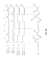
- FIGS. 2A-2B are diagrams illustrating examples of a magnetic waveform generator circuit 200 A with amplitude modulation capability and corresponding timing diagrams 210 , 212 , 214 , 216 , and 220 , according to certain embodiments.
- the magnetic waveform generator circuit 200 A is similar to the circuit 100 A of FIG. 1A , except for the additional switches S 3 and S 4 and capacitors C 3 and C 4 .
- the addition of the switches S 3 and S 4 and capacitors C 3 and C 4 enable circuit 200 A to generate a current i in the inductor L with a triangular waveform that can be amplitude modulated.
- the switches S 3 and S 4 are dipole switches that can be set to be connecting at either of two positions A or B.
- switches S 3 and S 4 When set to be at position A, the switches S 3 and S 4 , allow the capacitors C 3 and C 4 to be connected in series with the capacitors C 1 and C 2 , respectively.
- switches S 3 and S 4 are set to be connecting at position B, the circuit 200 becomes similar and operates similarly to the circuit 100 A.
- the switches S 3 and S 4 can be implemented as semiconductor dipole switches using known transistor or diode switch circuitry.
- capacitors C 3 and C 4 are connected in series with capacitors C 1 and C 2 to provide a higher voltage for driving the current i through the inductor L, which can form the high current amplitude of the amplitude modulated waveform, as shown in the timing diagram 220 of FIG. 2B .
- the drive circuitry, protection circuitry, power supplies, and internal resistors are not shown for simplicity
- the timing diagrams 210 , 212 , 214 , 216 shown in FIG. 2B are control pulses applied to switches S 1 through S 4 .
- the timing diagrams are shown for five consecutive cycles (e.g., periods) P 1 P 2 . . . P 5 .
- switches S 1 and S 2 are toggled as explained with respect to phases 100 C through 100 F of FIGS. 1C through 1F , and the switches S 3 and S 4 are set at position A, to allow capacitors C 3 and C 4 be connected in series with the capacitors C 1 and C 2 , thereby providing the high amplitude triangular waveform, as shown by waveform 222 .
- the amplitude of the triangular waveform may be reduced by removing the capacitors C 3 and C 4 from the circuit 200 A, thereby providing smaller voltage to drive the inductor current through the inductor L. This is done at cycle P 2 , where the switches S 3 and S 4 are both set to position B and switches S 1 and S 2 go through the phases to generate a triangular waveform as explained above.
- the ratio of amplitudes of the waveforms 222 and 224 depend on the capacitance values of the capacitors C 1 , C 2 , C 3 , and C 4 .
- the amplitude of the waveform 224 would be half of the amplitude of the waveform 222 .
- Other amplitude ratios can be achieved by suitably selecting the capacitance values of the capacitors C 1 , C 2 , C 3 , and C 4 .
- switches S 1 and S 2 are open and switches S 3 and S 4 are set at position 8 , and the charged capacitors C 1 have no path for driving current into the inductor L. Therefore, during cycle ⁇ P 3 , zero current passes through the inductor L.
- a recharge circuit (not shown for simplicity) can return the voltages of capacitors C 1 and C 2 to their desired level, correcting for resistive losses, without generating a current in the inductor and therefore without affecting the magnetic field.
- the waveforms 222 , 224 , 226 , and 228 can be used to represent, for example, binary symbols 11 , 10 , 01 , and 00 by a magnetic communications transmitter using the circuit 200 A as the magnetic field generator.
- the cycle P 3 which has no signal, can be used as the OFF symbol to allow for calibration, synchronization, and background cancellation in the receiver side.
- FIGS. 3A-3B are diagrams illustrating examples of an H-bridge magnetic waveform generator circuit 300 A and an H-bridge magnetic waveform generator circuit 300 B with amplitude modulation capability, according to certain embodiments.
- the bridge magnetic waveform generator circuit 300 A (hereinafter “circuit 300 A”) is similar to circuit 100 A of FIG. 1A , except for the additional switches S 3 and S 2 and diodes D 2 and D 3 and the fact that node 308 of the inductor L is not connected to the ground potential.
- the switch S 3 is coupled between nodes 304 and 308
- switch S 2 is coupled between nodes 308 and 306 .
- Diodes D 2 and D 3 are coupled in parallel with switches S 3 and S 2 , respectively.
- the capacitors C 1 and C 2 join at node 310 that is coupled to ground potential.
- the drive circuitry, protection circuitry, power supplies, and internal resistors e.g., for the inductor L
- switches S 2 and S 3 and diodes D 2 and D 3 can be implemented in the same semiconductor chip using transistor switches and semiconductor (e.g., silicon) diodes.
- FIG. 300A has the advantageous feature that allows using lower supply voltage values.
- the capacitors C 1 and C 2 can each be precharged to 50V (instead of 100V for circuit 100 A) and the circuit 300 A still provides the same amplitude triangular waveform for the current in the inductor L.
- the operation of the circuit 300 A includes four phases, during which status of switches S 1 , S 2 , S 3 , and S 4 are controlled to be different to allow suitable paths for flow of current from or to the capacitors C 1 and C 2 through the inductor L.
- switches S 1 and S 2 are closed and switches S 3 and S 4 are open, and diodes D 1 and D 2 are reverse biased.
- the capacitors C 1 and C 2 discharge to drive a positive increasing (up-ramping) current through the switches S 1 and S 2 and the inductor L.
- This current provides the first quarter-cycle of a triangular current waveform (e.g., 120 of FIG. 1B ).
- switches S 1 , S 2 , S 3 , and S 4 are open, and diodes D 1 and D 2 are forward biased and conduct current.
- the capacitors C 1 and C 2 recharge, which causes driving a positive decreasing (down-ramping) current through the diodes D 1 and D 2 into the inductor L. This current provides the second quarter-cycle of the triangular current waveform.
- switches S 3 and S 4 are closed and switches S 1 and S 2 are open, and diodes D 1 and D 2 are reverse biased.
- the capacitors C 1 and C 2 discharge to drive a negative (e.g., with revered direction) increasing amplitude current through the switches S 3 and S 4 and the inductor L.
- This current provides the third quarter-cycle of the triangular current waveform.
- switches S 1 , S 2 , S 3 , and S 4 are open, and diodes D 3 and D 4 are forward biased and conduct current.
- the capacitors C 1 and C 2 recharge and cause driving a negative decreasing current into the inductor L through diodes D 3 and D 4 .
- This current provides the fourth quarter-cycle of the triangular current waveform.
- the circuit 300 A can be modified to provide amplitude modulation as discussed herein.
- the H-bridge magnetic waveform generator circuit 300 B (hereinafter “circuit 300 B”) shown in FIG. 3B has amplitude modulation capability.
- the circuit 300 B has a portion 350 that is similar to the circuit 300 A and an additional portion 352 including an inductor L 2 , diodes D 5 and D 6 , and switches S 5 and S 6 .
- the inductor L 2 does not create an external magnetic field at long distances as, for example, a toroidal inductor.
- the inductor L 1 creates an external magnetic waveform as, for example, a magnetic coil.
- the operation of portion 350 is also similar to the operation of circuit 300 A, as discussed above.
- the portion 350 is used to generate a high (e.g., maximum)-amplitude triangular current waveform (e.g., 222 of FIG. 2B ), during the four phased as discussed above with respect to FIG. 3A .
- switches S 5 and S 6 are open.
- the portion 352 comes into the play and switches S 5 and S 6 are suitably opened or closed (while S 1 and S 4 are kept open) to allow driving currents in two different directions, as explained above, into series connected inductors L 1 and L 2 .
- the series connection of inductors L 1 and L 2 increases the impedance in the path of the current and thereby decrease the amplitude of the current passing through the inductors L 1 and L 2 .
- the ratio of amplitudes of the low-amplitude and high-amplitude waveforms depend on the inductance values of the inductors L 1 and L 2 . For example, if the inductance values of the inductors L 1 and L 2 are the same, the amplitude of the low-amplitude waveform would be half of the amplitude of the high-amplitude waveform. Other amplitude ratios can be achieved by suitably selecting the inductance values of the inductors L 1 and L 2 .
- FIG. 4 is a diagram illustrating an example of a method 400 for providing a magnetic waveform generator circuit, according to certain embodiments.
- a first switch e.g., S 1 of FIG. 1A
- a first rectifier element e.g., D 1 of FIG. 1A
- a first capacitor e.g., C 1 of FIG. 1A
- a second node e.g., 104 of FIG. 1A
- a fourth node e.g., 108 of FIG. 1A
- a second capacitor may be coupled, at a third node (e.g., 106 of FIG. 1A ) to the first rectifier element, and to the forth node ( 430 ).
- An inductor e.g., L of FIG. 1A
- the first switch is operable to be in an ON state during a first time period (e.g., T 1 of FIG. 1B ) and in an off state during a second time period (e.g., T 2 of FIG. 1B ).
- the first switch and the first rectifier element are configured to enable the inductor to generate, during the first and the second time periods, a magnetic field having a waveform resembling a positive half-cycle of a triangular waveform (e.g., 120 of FIG. 1B ).
- compositions and methods are described in terms of “comprising,” “containing,” or “including” various components or steps, the compositions and methods can also “consist essentially of” or “consist of” the various components and operations. All numbers and ranges disclosed above can vary by some amount. Whenever a numerical range with a lower limit and an upper limit is disclosed, any number and any subrange falling within the broader range is specifically disclosed. Also, the terms in the claims have their plain, ordinary meaning unless otherwise explicitly and clearly defined by the patentee. If there is any conflict in the usages of a word or term in this specification and one or more patent or other documents that may be incorporated herein by reference, the definitions that are consistent with this specification should be adopted.
Abstract
Description
Claims (14)
Priority Applications (4)
| Application Number | Priority Date | Filing Date | Title |
|---|---|---|---|
| US14/680,877 US9590601B2 (en) | 2014-04-07 | 2015-04-07 | Energy efficient controlled magnetic field generator circuit |
| US15/179,957 US9910105B2 (en) | 2014-03-20 | 2016-06-10 | DNV magnetic field detector |
| US15/450,504 US10277208B2 (en) | 2014-04-07 | 2017-03-06 | Energy efficient controlled magnetic field generator circuit |
| US15/912,461 US10725124B2 (en) | 2014-03-20 | 2018-03-05 | DNV magnetic field detector |
Applications Claiming Priority (2)
| Application Number | Priority Date | Filing Date | Title |
|---|---|---|---|
| US201461975997P | 2014-04-07 | 2014-04-07 | |
| US14/680,877 US9590601B2 (en) | 2014-04-07 | 2015-04-07 | Energy efficient controlled magnetic field generator circuit |
Related Parent Applications (2)
| Application Number | Title | Priority Date | Filing Date |
|---|---|---|---|
| US14/659,498 Continuation-In-Part US9638821B2 (en) | 2014-03-20 | 2015-03-16 | Mapping and monitoring of hydraulic fractures using vector magnetometers |
| US14/676,740 Continuation-In-Part US9853837B2 (en) | 2014-03-20 | 2015-04-01 | High bit-rate magnetic communication |
Related Child Applications (3)
| Application Number | Title | Priority Date | Filing Date |
|---|---|---|---|
| US14/866,730 Continuation-In-Part US10168393B2 (en) | 2014-03-20 | 2015-09-25 | Micro-vacancy center device |
| US15/179,957 Continuation-In-Part US9910105B2 (en) | 2014-03-20 | 2016-06-10 | DNV magnetic field detector |
| US15/450,504 Continuation US10277208B2 (en) | 2014-04-07 | 2017-03-06 | Energy efficient controlled magnetic field generator circuit |
Publications (2)
| Publication Number | Publication Date |
|---|---|
| US20150288352A1 US20150288352A1 (en) | 2015-10-08 |
| US9590601B2 true US9590601B2 (en) | 2017-03-07 |
Family
ID=54210649
Family Applications (2)
| Application Number | Title | Priority Date | Filing Date |
|---|---|---|---|
| US14/680,877 Expired - Fee Related US9590601B2 (en) | 2014-03-20 | 2015-04-07 | Energy efficient controlled magnetic field generator circuit |
| US15/450,504 Active US10277208B2 (en) | 2014-04-07 | 2017-03-06 | Energy efficient controlled magnetic field generator circuit |
Family Applications After (1)
| Application Number | Title | Priority Date | Filing Date |
|---|---|---|---|
| US15/450,504 Active US10277208B2 (en) | 2014-04-07 | 2017-03-06 | Energy efficient controlled magnetic field generator circuit |
Country Status (4)
| Country | Link |
|---|---|
| US (2) | US9590601B2 (en) |
| CA (1) | CA2945016A1 (en) |
| GB (1) | GB2540308B (en) |
| WO (1) | WO2015157290A1 (en) |
Cited By (42)
| Publication number | Priority date | Publication date | Assignee | Title |
|---|---|---|---|---|
| US9720055B1 (en) | 2016-01-21 | 2017-08-01 | Lockheed Martin Corporation | Magnetometer with light pipe |
| US9824597B2 (en) | 2015-01-28 | 2017-11-21 | Lockheed Martin Corporation | Magnetic navigation methods and systems utilizing power grid and communication network |
| US9823314B2 (en) | 2016-01-21 | 2017-11-21 | Lockheed Martin Corporation | Magnetometer with a light emitting diode |
| US9823381B2 (en) | 2014-03-20 | 2017-11-21 | Lockheed Martin Corporation | Mapping and monitoring of hydraulic fractures using vector magnetometers |
| US9835693B2 (en) | 2016-01-21 | 2017-12-05 | Lockheed Martin Corporation | Higher magnetic sensitivity through fluorescence manipulation by phonon spectrum control |
| US9845153B2 (en) | 2015-01-28 | 2017-12-19 | Lockheed Martin Corporation | In-situ power charging |
| US9853837B2 (en) | 2014-04-07 | 2017-12-26 | Lockheed Martin Corporation | High bit-rate magnetic communication |
| US9910104B2 (en) | 2015-01-23 | 2018-03-06 | Lockheed Martin Corporation | DNV magnetic field detector |
| US9910105B2 (en) | 2014-03-20 | 2018-03-06 | Lockheed Martin Corporation | DNV magnetic field detector |
| US10006973B2 (en) | 2016-01-21 | 2018-06-26 | Lockheed Martin Corporation | Magnetometer with a light emitting diode |
| US10012704B2 (en) | 2015-11-04 | 2018-07-03 | Lockheed Martin Corporation | Magnetic low-pass filter |
| US10088336B2 (en) | 2016-01-21 | 2018-10-02 | Lockheed Martin Corporation | Diamond nitrogen vacancy sensed ferro-fluid hydrophone |
| US10088452B2 (en) | 2016-01-12 | 2018-10-02 | Lockheed Martin Corporation | Method for detecting defects in conductive materials based on differences in magnetic field characteristics measured along the conductive materials |
| US10120039B2 (en) | 2015-11-20 | 2018-11-06 | Lockheed Martin Corporation | Apparatus and method for closed loop processing for a magnetic detection system |
| US10126377B2 (en) | 2016-05-31 | 2018-11-13 | Lockheed Martin Corporation | Magneto-optical defect center magnetometer |
| US10145910B2 (en) | 2017-03-24 | 2018-12-04 | Lockheed Martin Corporation | Photodetector circuit saturation mitigation for magneto-optical high intensity pulses |
| US10168393B2 (en) | 2014-09-25 | 2019-01-01 | Lockheed Martin Corporation | Micro-vacancy center device |
| US10228429B2 (en) | 2017-03-24 | 2019-03-12 | Lockheed Martin Corporation | Apparatus and method for resonance magneto-optical defect center material pulsed mode referencing |
| US10241158B2 (en) | 2015-02-04 | 2019-03-26 | Lockheed Martin Corporation | Apparatus and method for estimating absolute axes' orientations for a magnetic detection system |
| US10277208B2 (en) * | 2014-04-07 | 2019-04-30 | Lockheed Martin Corporation | Energy efficient controlled magnetic field generator circuit |
| US10274550B2 (en) | 2017-03-24 | 2019-04-30 | Lockheed Martin Corporation | High speed sequential cancellation for pulsed mode |
| US10281550B2 (en) | 2016-11-14 | 2019-05-07 | Lockheed Martin Corporation | Spin relaxometry based molecular sequencing |
| US10317279B2 (en) | 2016-05-31 | 2019-06-11 | Lockheed Martin Corporation | Optical filtration system for diamond material with nitrogen vacancy centers |
| US10330744B2 (en) | 2017-03-24 | 2019-06-25 | Lockheed Martin Corporation | Magnetometer with a waveguide |
| US10333588B2 (en) | 2015-12-01 | 2019-06-25 | Lockheed Martin Corporation | Communication via a magnio |
| US10338164B2 (en) | 2017-03-24 | 2019-07-02 | Lockheed Martin Corporation | Vacancy center material with highly efficient RF excitation |
| US10338162B2 (en) | 2016-01-21 | 2019-07-02 | Lockheed Martin Corporation | AC vector magnetic anomaly detection with diamond nitrogen vacancies |
| US10338163B2 (en) | 2016-07-11 | 2019-07-02 | Lockheed Martin Corporation | Multi-frequency excitation schemes for high sensitivity magnetometry measurement with drift error compensation |
| US10345395B2 (en) | 2016-12-12 | 2019-07-09 | Lockheed Martin Corporation | Vector magnetometry localization of subsurface liquids |
| US10345396B2 (en) | 2016-05-31 | 2019-07-09 | Lockheed Martin Corporation | Selected volume continuous illumination magnetometer |
| US10359479B2 (en) | 2017-02-20 | 2019-07-23 | Lockheed Martin Corporation | Efficient thermal drift compensation in DNV vector magnetometry |
| US10371765B2 (en) | 2016-07-11 | 2019-08-06 | Lockheed Martin Corporation | Geolocation of magnetic sources using vector magnetometer sensors |
| US10371760B2 (en) | 2017-03-24 | 2019-08-06 | Lockheed Martin Corporation | Standing-wave radio frequency exciter |
| US10379174B2 (en) | 2017-03-24 | 2019-08-13 | Lockheed Martin Corporation | Bias magnet array for magnetometer |
| US10408889B2 (en) | 2015-02-04 | 2019-09-10 | Lockheed Martin Corporation | Apparatus and method for recovery of three dimensional magnetic field from a magnetic detection system |
| US10408890B2 (en) | 2017-03-24 | 2019-09-10 | Lockheed Martin Corporation | Pulsed RF methods for optimization of CW measurements |
| US10459041B2 (en) | 2017-03-24 | 2019-10-29 | Lockheed Martin Corporation | Magnetic detection system with highly integrated diamond nitrogen vacancy sensor |
| US10466312B2 (en) | 2015-01-23 | 2019-11-05 | Lockheed Martin Corporation | Methods for detecting a magnetic field acting on a magneto-optical detect center having pulsed excitation |
| US10520558B2 (en) | 2016-01-21 | 2019-12-31 | Lockheed Martin Corporation | Diamond nitrogen vacancy sensor with nitrogen-vacancy center diamond located between dual RF sources |
| US10527746B2 (en) | 2016-05-31 | 2020-01-07 | Lockheed Martin Corporation | Array of UAVS with magnetometers |
| US10571530B2 (en) | 2016-05-31 | 2020-02-25 | Lockheed Martin Corporation | Buoy array of magnetometers |
| US10677953B2 (en) | 2016-05-31 | 2020-06-09 | Lockheed Martin Corporation | Magneto-optical detecting apparatus and methods |
Families Citing this family (3)
| Publication number | Priority date | Publication date | Assignee | Title |
|---|---|---|---|---|
| CN110661433A (en) * | 2019-09-16 | 2020-01-07 | 西安西电电力系统有限公司 | Power electronic transformer |
| DE102021101577A1 (en) | 2020-01-30 | 2021-08-05 | Elmos Semiconductor Se | Optical system with NV centers and optically transparent film structures |
| US11128171B1 (en) * | 2020-12-11 | 2021-09-21 | Global Energy Applications, LLC | Supplemental electromagnetic circuit |
Citations (222)
| Publication number | Priority date | Publication date | Assignee | Title |
|---|---|---|---|---|
| US2746027A (en) | 1951-11-16 | 1956-05-15 | James J Murray | Flux-gap variation transducer for hydrophones, microphones, and accelerometers |
| US3389333A (en) | 1964-02-10 | 1968-06-18 | Sperry Rand Corp | Control system for maintaining a desired magnetic field in a given space |
| US3514723A (en) | 1966-06-23 | 1970-05-26 | Warwick Electronics Inc | Tone control circuit comprising a single potentiometer |
| US3518531A (en) | 1968-02-23 | 1970-06-30 | Varian Associates | Transient suppressor for use in magnetometer readout circuits |
| US3745452A (en) | 1971-02-23 | 1973-07-10 | J Osburn | Magnetic field gradient apparatus and method for detecting pipe line corrosion |
| US3899758A (en) | 1974-05-01 | 1975-08-12 | Gte International Inc | Variable inductive resonant circuit arrangement having a diamagnetic core for the UHF range |
| US4078247A (en) * | 1975-02-05 | 1978-03-07 | Rca Corporation | Inverter circuit control circuit for precluding simultaneous conduction of thyristors |
| US4084215A (en) | 1977-02-25 | 1978-04-11 | The United States Of America As Represented By The Secretary Of The Navy | Strobe light having reduced electromagnetic radiation |
| US4329173A (en) | 1980-03-31 | 1982-05-11 | Carondelet Foundry Company | Alloy resistant to corrosion |
| US4368430A (en) | 1980-08-18 | 1983-01-11 | Sanders Associates, Inc. | Fiber optic magnetic sensors |
| US4514083A (en) | 1981-02-03 | 1985-04-30 | Olympus Optical Company Ltd. | Distance measuring apparatus |
| US4588993A (en) | 1980-11-26 | 1986-05-13 | The United States Of America As Represented By The Secretary Of The Department Of Health And Human Services | Broadband isotropic probe system for simultaneous measurement of complex E- and H-fields |
| US4638324A (en) | 1984-12-10 | 1987-01-20 | Hazeltine Corporation | Resistive loop angular filter |
| US4675522A (en) | 1985-10-09 | 1987-06-23 | Spectron Development Laboratories, Inc. | Fiber optic magnetic field sensor |
| WO1987004028A1 (en) | 1985-12-20 | 1987-07-02 | Pierre Misson | Magnetic transmission |
| WO1988004032A1 (en) | 1986-11-27 | 1988-06-02 | Plessey Overseas Limited | Acoustic sensor |
| US4945305A (en) | 1986-10-09 | 1990-07-31 | Ascension Technology Corporation | Device for quantitatively measuring the relative position and orientation of two bodies in the presence of metals utilizing direct current magnetic fields |
| EP0161940B1 (en) | 1984-05-17 | 1990-12-27 | Electricity Association Services Limited | Radio direction finding for locating lightening ground strikes |
| US5019721A (en) | 1989-08-18 | 1991-05-28 | Wisconsin Alumni Research Foundation | Active superconducting devices formed of thin films |
| US5038103A (en) | 1985-04-22 | 1991-08-06 | The United States Of America As Represented By The Secretary Of The Navy | Optical fiber magnetometer |
| US5113136A (en) | 1989-01-20 | 1992-05-12 | Fujitsu Limited | Gradiometer apparatus with compensation coils for measuring magnetic fields |
| US5134369A (en) | 1991-03-12 | 1992-07-28 | Hughes Aircraft Company | Three axis magnetometer sensor field alignment and registration |
| US5189368A (en) | 1976-09-24 | 1993-02-23 | Lockheed Sanders, Inc. | Magnetometer |
| US5245347A (en) | 1980-12-29 | 1993-09-14 | Raytheon Company | All weather tactical strike system (AWTSS) and method of operation |
| US5252912A (en) | 1989-06-28 | 1993-10-12 | William E. Merritt | System for warning aircraft pilot of potential impact with a power line and generating time-to-time impact signal |
| US5301096A (en) | 1991-09-27 | 1994-04-05 | Electric Power Research Institute | Submersible contactless power delivery system |
| US5384109A (en) | 1990-04-02 | 1995-01-24 | Nycomed Imaging As | Diagnostic magnetometry using superparamagnetic particles |
| US5396802A (en) | 1993-08-26 | 1995-03-14 | Viatran Corporation | Differential pressure transducer utilizing a variable ferrofluid keeper as an active magnetic circuit element |
| WO1995033972A1 (en) | 1994-06-02 | 1995-12-14 | Spectra-Physics Laserplane, Inc. | Laser alignment device and method using green light |
| EP0718642A1 (en) | 1994-12-20 | 1996-06-26 | De Beers Industrial Diamond Division (Proprietary) Limited | Diffractive optics |
| US5568516A (en) | 1993-07-02 | 1996-10-22 | Phonic Ear Incorporated | Very low power cordless headset system |
| US5694375A (en) | 1996-03-22 | 1997-12-02 | The United States Of America As Represented By The Secretary Of The Navy | Ultra-broadband hydrophone |
| US5818352A (en) | 1994-09-03 | 1998-10-06 | Integrated Drilling Services Limited | Well data telemetry system |
| US5907420A (en) | 1996-09-13 | 1999-05-25 | Lucent Technologies, Inc. | System and method for mitigating cross-saturation in optically amplified networks |
| US6057684A (en) | 1995-10-31 | 2000-05-02 | Yoshihiro Murakami | Magnetic flaw detection apparatus using an E-shaped magnetic sensor and high-pass filter |
| EP0726458B1 (en) | 1995-01-13 | 2000-05-03 | Bruker Analytik Gmbh | Method and apparatus for detecting gemstones within a surrounding substance by means of nuclear magnetic resonance |
| US6124862A (en) | 1997-06-13 | 2000-09-26 | Anivision, Inc. | Method and apparatus for generating virtual views of sporting events |
| US6130753A (en) | 1999-02-01 | 2000-10-10 | The United States Of America As Represented By The Secretary Of The Air Force | Laser optical density measurement system |
| US6195231B1 (en) | 1994-05-06 | 2001-02-27 | Steven R. Sedlmayr | Thin film magnetic data transfer transducer |
| US6360173B1 (en) | 1999-02-22 | 2002-03-19 | Terrescan Technologies, Inc. | Geophysical exploration system and method |
| US6398155B1 (en) | 2001-01-02 | 2002-06-04 | The United States Of America As Represented By The Secretary Of The Army | Method and system for determining the pointing direction of a body in flight |
| US6433944B1 (en) | 1998-09-25 | 2002-08-13 | Fuji Photo Film Co., Ltd. | Master carrier for magnetic transfer and method for transfer |
| US20020167306A1 (en) | 2001-03-23 | 2002-11-14 | Ivano Zalunardo | Device with a magnetic position encoder |
| US6504365B2 (en) | 2000-09-29 | 2003-01-07 | Jeol Ltd. | Magnetic force microscope |
| DE10228536A1 (en) | 2001-06-26 | 2003-01-30 | Fuji Photo Film Co Ltd | Magnetic recording medium used in magnetic disks in mini computers, personal computers, and work stations comprises a support with a non-magnetic lower layer, and a magnetic layer |
| US20030058346A1 (en) | 1997-04-02 | 2003-03-27 | Bechtel Jon H. | Control circuit for image array sensors |
| US6542242B1 (en) | 1999-05-10 | 2003-04-01 | University Of Washington | Mapping air contaminants using path-integrated optical remote sensing with a non-overlapping variable path length beam geometry |
| US20030076229A1 (en) | 2000-03-14 | 2003-04-24 | Roland Blanpain | Microsystem using magnetometer and inclinometer for anti-theft protection of valuables |
| US6636146B1 (en) | 1996-12-10 | 2003-10-21 | Régie Autonome des Transports Parisiens | Contactless communication system for exchanging data |
| US20030235136A1 (en) | 2001-12-04 | 2003-12-25 | Mark Akselrod | Optical single-bit recording and fluorescent readout utilizing aluminum oxide single crystals |
| US20040013180A1 (en) | 2002-04-22 | 2004-01-22 | Giannakis Georgios B. | Space-time multipath coding schemes for wireless communication systems |
| US6686696B2 (en) | 2001-03-08 | 2004-02-03 | Genvac Aerospace Corporation | Magnetron with diamond coated cathode |
| US20040022179A1 (en) | 2002-04-22 | 2004-02-05 | Giannakis Georgios B. | Wireless communication system having error-control coder and linear precoder |
| US6690162B1 (en) | 1999-10-04 | 2004-02-10 | Qest Quantenelektronische Systeme | Device for high-resolution measurement of magnetic fields |
| US20040042150A1 (en) | 2000-01-27 | 2004-03-04 | Swinbanks Malcolm A. | Dynamic degaussing system |
| US20040109328A1 (en) | 2002-12-06 | 2004-06-10 | Chevron U.S.A. Inc. | Optical uses of diamondoid-containing materials |
| US20040247145A1 (en) | 2003-06-03 | 2004-12-09 | Unitron Hearing Ltd. | Automatic magnetic detection in hearing aids |
| US20050099177A1 (en) | 2003-11-06 | 2005-05-12 | Greelish Stephen J. | Dynamic magnetic anomaly compensation |
| US20050126905A1 (en) | 1999-06-22 | 2005-06-16 | President And Fellows Of Harvard College | High-precision feedback control for ion sculpting of solid state features |
| US20050130601A1 (en) | 2001-03-16 | 2005-06-16 | Vincent Palermo | Methods and apparatus for tuning in an inductive system |
| US20050134257A1 (en) | 2003-12-22 | 2005-06-23 | Kurt Etherington | Combination hall effect position sensor and switch |
| US20050146327A1 (en) | 1998-12-23 | 2005-07-07 | Jakab Peter D. | Magnetic resonance scanner with electromagnetic position and orientation tracking device |
| US20060054789A1 (en) | 2004-09-13 | 2006-03-16 | Matsushita Electric Industrial Co., Ltd | Photodetector-amplifier circuit and optical pickup device |
| US20060062084A1 (en) | 2004-09-17 | 2006-03-23 | Julian Drew | Microseismic event detection and location by continuous map migration |
| US20060071709A1 (en) | 2003-12-31 | 2006-04-06 | Franco Maloberti | Switched-capacitor circuits with reduced finite-gain effect |
| EP1685597A2 (en) | 2003-11-18 | 2006-08-02 | Halliburton Energy Services, Inc. | High-temperature devices on insulator substrates |
| US7118657B2 (en) | 1999-06-22 | 2006-10-10 | President And Fellows Of Harvard College | Pulsed ion beam control of solid state features |
| US20070004371A1 (en) | 2001-06-08 | 2007-01-04 | Sony Corporation | IC receiver to minimize tracking error |
| US7221164B1 (en) | 2006-04-25 | 2007-05-22 | Barringer Anthony R | Airborne remote sensing electric field exploration system |
| GB2433737B (en) | 2002-11-21 | 2007-08-15 | Element Six Ltd | Optical quality diamond material |
| US7277161B2 (en) | 2004-11-10 | 2007-10-02 | Wetenschappelijk En Technisch Onderzoekscentrum Voor Diamant | Method for discerning colorless and near colorless diamonds and arrangement for carrying out this method |
| US20070247147A1 (en) | 2001-10-25 | 2007-10-25 | Intermatix Corporation | Detection with evanescent wave probe |
| US7307416B2 (en) | 2004-10-22 | 2007-12-11 | Delphi Technologies, Inc. | Position sensor and assembly |
| US7305869B1 (en) | 2004-04-12 | 2007-12-11 | U. S. Department Of Energy | Spin microscope based on optically detected magnetic resonance |
| US20080016677A1 (en) | 2002-01-23 | 2008-01-24 | Stereotaxis, Inc. | Rotating and pivoting magnet for magnetic navigation |
| US20080048640A1 (en) | 2006-08-18 | 2008-02-28 | Hull David M | Methods for detecting and classifying loads on AC lines |
| US20080078233A1 (en) | 2006-09-25 | 2008-04-03 | Larson John D | Apparatus and method for measuring an environmental condition |
| US20080089367A1 (en) | 2006-10-03 | 2008-04-17 | Kartik Srinivasan | Fiber-Coupled Solid State Microcavity Light Emitters |
| USRE40343E1 (en) | 1997-01-09 | 2008-05-27 | Cymer, Inc. | Control circuit with automatic DC offset |
| US7413011B1 (en) | 2007-12-26 | 2008-08-19 | Schlumberger Technology Corporation | Optical fiber system and method for wellhole sensing of magnetic permeability using diffraction effect of faraday rotator |
| US20080204004A1 (en) | 2007-02-23 | 2008-08-28 | General Electric Company | Coil arrangement for electromagnetic tracking method and system |
| US20080217516A1 (en) | 2004-07-22 | 2008-09-11 | Hamamatsu Photonics K.K. | Photodetector |
| US7427525B2 (en) | 2006-10-13 | 2008-09-23 | Hewlett-Packard Development Company, L.P. | Methods for coupling diamond structures to photonic devices |
| US20080239265A1 (en) | 2007-03-30 | 2008-10-02 | Asml Netherlands B.V. | Angularly resolved scatterometer, inspection method, lithographic apparatus, lithographic processing cell device manufacturing method and alignment sensor |
| US7448548B1 (en) | 2006-01-13 | 2008-11-11 | Point Six Wireless, Llc | Pulsed wireless directional object counter |
| EP1990313A1 (en) | 2007-05-10 | 2008-11-12 | INSERM (Institut National de la Santé et de la Recherche Médicale) | Method to produce light-emitting nano-particles of diamond |
| US20080299904A1 (en) | 2007-06-04 | 2008-12-04 | Seagate Technology Llc | Wireless communication system |
| US7471805B2 (en) | 2004-12-20 | 2008-12-30 | Central Coast Patent Agency, Inc. | Hearing aid mechanism |
| US20090042592A1 (en) | 2007-07-06 | 2009-02-12 | Lg Electronics Inc. | Broadcast receiver and method of processing data |
| US20090060790A1 (en) | 2006-06-16 | 2009-03-05 | Murata Manufacturing Co., Ltd. | Sensor for detecting substance in liquid |
| US20090079426A1 (en) | 2007-09-25 | 2009-03-26 | General Electric Company, A New York Corporation | Electromagnetic tracking employing scalar-magnetometer |
| US20090132100A1 (en) | 2005-03-18 | 2009-05-21 | Hideki Shibata | Flight Control System |
| US7546000B2 (en) | 2006-09-07 | 2009-06-09 | Hewlett-Packard Development Company, L.P. | Scalable and defect-tolerant color-center-based quantum computer architectures and methods for fabricating color-center-based quantum computer architectures |
| US7543780B1 (en) | 2004-10-04 | 2009-06-09 | The United States Of America As Represented By The Secretary Of The Air Force | Unmanned air vehicle transmission line docking surveillance |
| EP1505627B1 (en) | 2003-08-07 | 2009-10-14 | Panasonic Corporation | Magnetron |
| US20090277702A1 (en) | 2005-10-07 | 2009-11-12 | Toyota Jidosha Kabushiki Kaisha | Hybrid vehicle and method of controlling the same |
| US20090310650A1 (en) | 2008-06-12 | 2009-12-17 | Harris Corporation | Featureless coherent chaotic amplitude modulation |
| US20100045269A1 (en) | 2001-03-16 | 2010-02-25 | Lafranchise Jeffrey R | Methods and apparatus to detect location and orientation in an inductive system |
| US20100134922A1 (en) | 2008-11-28 | 2010-06-03 | Kabushiki Kaisha Toshiba | Magnetic recording head, magnetic head assembly, magnetic recording apparatus, and magnetic recording method |
| US20100157305A1 (en) | 2008-12-18 | 2010-06-24 | Henderson Thomas A | In-line self spacing optical sensor assembly for a printer |
| US20100188081A1 (en) | 2007-06-15 | 2010-07-29 | Technische Universitat Graz | Method and Device for Measuring Magnetic Fields |
| US20100237149A1 (en) | 2009-03-17 | 2010-09-23 | Datalogic Scanning, Inc. | Systems and methods for compensating for fixed pattern noise |
| EP2163392B1 (en) | 2008-09-10 | 2010-10-06 | OOO "Novye Energeticheskie Tehnologii" | Document security, securities and article protection method using nanodiamonds with active NV centers |
| US20100271016A1 (en) | 2009-04-24 | 2010-10-28 | Hewlett-Packard Development Company, L.P. | Microfiber Magnetometer |
| US20100308813A1 (en) | 2007-12-03 | 2010-12-09 | President And Fellows Of Harvard College | High sensitivity solid state magnetometer |
| US20100326042A1 (en) | 2008-11-25 | 2010-12-30 | Mclean John P | Efficient RF Electromagnetic Propulsion System With Communications Capability |
| US20110034393A1 (en) | 2007-09-25 | 2011-02-10 | Lesaffre Et Compagnie | Use of a novel natural agent in cosmetic compositions |
| US20110062957A1 (en) | 2009-09-11 | 2011-03-17 | Hewlett-Packard Development Company, L.P. | Optically integrated biosensor based on optically detected magnetic resonance |
| US20110063957A1 (en) | 2009-09-16 | 2011-03-17 | Hitachi Media Electronics Co., Ltd. | Optical disk apparatus |
| US20110066379A1 (en) | 2008-05-26 | 2011-03-17 | Mes Marius J | survey system for locating geophysical anomalies |
| WO2011046403A2 (en) | 2009-10-16 | 2011-04-21 | Korea Advanced Institute Of Science And Technology | Autonomous driving apparatus and method of on-line electric vehicle |
| US20110127999A1 (en) | 2009-08-14 | 2011-06-02 | Paul Lott | Pipeline inspection apparatus and method |
| US20110165862A1 (en) | 2008-11-26 | 2011-07-07 | Nationz Technologies Inc. | Rf sim card, card reader, and communication method |
| US7983812B2 (en) | 2008-08-04 | 2011-07-19 | Scott Potter & Associates, Llc | Method and apparatus for managing battery power in emergency vehicles |
| US20110243267A1 (en) | 2010-03-31 | 2011-10-06 | Korea Electronics Technology Institute | Magnetic field communication method for managing node with low power consumption |
| JP4800896B2 (en) | 2006-10-16 | 2011-10-26 | シャープ株式会社 | Magnetic sensor element and manufacturing method thereof, magnetic head, magnetic reproducing apparatus, and magnetic reproducing method |
| WO2011153339A1 (en) | 2010-06-02 | 2011-12-08 | William Marsh Rice University | Magnetic particles for determining reservoir parameters |
| US20120016538A1 (en) | 2010-06-21 | 2012-01-19 | Waite James W | Uav power line position and load parameter estimation |
| US20120019242A1 (en) | 2008-11-04 | 2012-01-26 | The University Of Melbourne | Method and apparatus for monitoring a property of a sample |
| WO2012016977A2 (en) | 2010-08-04 | 2012-02-09 | Element Six Limited | A diamond optical element |
| US20120037803A1 (en) | 2010-08-12 | 2012-02-16 | Flir Systems, Inc. | Electromagnetic interference shield |
| US8120355B1 (en) | 2009-05-27 | 2012-02-21 | Lockheed Martin Corporation | Magnetic anomaly detector |
| US8120351B2 (en) | 2004-03-11 | 2012-02-21 | Robert Bosch Gmbh | Magnet sensor arrangement for sensing the movement of element moving in linear or rotary fashion |
| US20120044014A1 (en) | 2010-08-18 | 2012-02-23 | Volterra Semiconductor Corporation | Switching Circuits For Extracting Power From An Electric Power Source And Associated Methods |
| US20120051996A1 (en) | 2008-07-23 | 2012-03-01 | Geoffrey Alan Scarsbrook | Diamond material |
| US20120063505A1 (en) | 2010-09-10 | 2012-03-15 | Panasonic Corporation | Power transmitter and wireless power transmission system |
| US20120087449A1 (en) | 2009-12-27 | 2012-04-12 | Curtis Ling | Methods and apparatus for synchronization in multiple-channel communication systems |
| JP2012103171A (en) | 2010-11-11 | 2012-05-31 | Jeol Resonance Inc | Magnetic field measuring device |
| US20120140219A1 (en) | 2010-12-07 | 2012-06-07 | Cleary Joseph A | Monolithic Geared Optical Reflector |
| JP2012110489A (en) | 2010-11-24 | 2012-06-14 | Sumitomo Electric Ind Ltd | Magnetism measuring instrument, and method for manufacturing magnetism sensor element |
| JP2012121748A (en) | 2010-12-07 | 2012-06-28 | Sumitomo Electric Ind Ltd | Diamond and magnetic sensor using the same |
| WO2012084750A1 (en) | 2010-12-24 | 2012-06-28 | Element Six Limited | Dislocation engineering in single crystal synthetic diamond material |
| US20120181020A1 (en) | 2008-05-20 | 2012-07-19 | Oxane Materials, Inc. | Method Of Manufacture And The Use Of A Functional Proppant For Determination Of Subterranean Fracture Geometries |
| US20120194068A1 (en) | 2011-01-31 | 2012-08-02 | Lite-On Technology Corp. | Lamp having light sensor |
| EP2495166A1 (en) | 2011-03-03 | 2012-09-05 | Asociacion de la Industria Navarra (AIN) | Aerial robotic system for the inspection of overhead power lines |
| US20120257683A1 (en) | 2009-12-30 | 2012-10-11 | Sony Corporation | Communications system using beamforming |
| US8294306B2 (en) | 2010-03-16 | 2012-10-23 | Indian Institute Of Technology Madras | DC capacitor balancing |
| US20120281843A1 (en) | 2011-05-06 | 2012-11-08 | Oticon A/S | Receiver and method for retrieving an information signal from a magnetic induction signal |
| US8311767B1 (en) | 2009-07-13 | 2012-11-13 | Lockheed Martin Corporation | Magnetic navigation system |
| US8334690B2 (en) | 2009-08-07 | 2012-12-18 | The United States of America as represented by the Secretary of Commerce, the National Institute of Standards and Technology | Atomic magnetometer and method of sensing magnetic fields |
| US20120326793A1 (en) | 2008-02-07 | 2012-12-27 | Lahav Gan | Device, system, and method of frequency generation using an atomic resonator |
| JP2013028497A (en) | 2011-07-28 | 2013-02-07 | Sumitomo Electric Ind Ltd | Polycrystalline diamond and method for producing the same |
| US8415640B2 (en) | 2010-04-19 | 2013-04-09 | President And Fellows Of Harvard College | Diamond nanowires |
| GB2495632A (en) | 2011-10-14 | 2013-04-17 | Element Six Ltd | A solid state component device for achieving multi-photon interference between quantum registers with nuclear and electron spin state coupling |
| EP2587232A1 (en) | 2011-10-27 | 2013-05-01 | Universität des Saarlandes | System and method for detecting mechanical vibrations |
| WO2013066446A1 (en) | 2011-08-01 | 2013-05-10 | The Trustees Of Columbia University In The City Of New York | Conjugates of nano-diamond and magnetic or metallic particles |
| WO2013066448A2 (en) | 2011-08-08 | 2013-05-10 | Battelle Memorial Institute | Polymer-sulfur composite materials for electrodes in li-s energy storage devices |
| US20130127518A1 (en) | 2011-11-18 | 2013-05-23 | Fujitsu Limited | Control circuit and electronic device |
| GB2483767B (en) | 2010-09-14 | 2013-05-29 | Element Six Ltd | A microfluidic cell and a spin resonance device for use therewith |
| US8471137B2 (en) | 2011-02-22 | 2013-06-25 | Kenneth Michael ADAIR | Pickup system with a cartridge |
| WO2013093136A1 (en) | 2011-12-23 | 2013-06-27 | Universidad De Zaragoza | Device and method for sensing magnetic materials |
| US8480653B2 (en) | 2007-05-23 | 2013-07-09 | Biosense Webster, Inc. | Magnetically guided catheter with concentric needle port |
| US20130215712A1 (en) | 2011-03-23 | 2013-08-22 | Global Geophysical Services, Inc. | Method for Assessing the Effectiveness of Modifying Transmissive Networks of Natural Reservoirs |
| US8525516B2 (en) | 2007-12-11 | 2013-09-03 | Commissariat à l'énergie atomique et aux énergies alternatives | Apparatus with ambient magnetic field correction |
| US20130265782A1 (en) | 2010-12-15 | 2013-10-10 | Illinois Tool Works Inc. | Heat-sink/connector system for light emitting diode |
| US8575929B1 (en) | 2011-06-20 | 2013-11-05 | The United States Of America As Represented By The Secretary Of The Navy | Magnetic anomaly surveillance system using spherical trilateration |
| GB2491936B (en) | 2011-05-24 | 2013-11-13 | Element Six Ltd | Diamond sensors detectors and quantum devices |
| WO2013188732A1 (en) | 2012-06-14 | 2013-12-19 | The Trustees Of Columbia University In The City Of New York | Systems and methods for precision optical imaging of electrical currents and temperature in integrated circuits |
| US20140012505A1 (en) | 2011-03-31 | 2014-01-09 | Laurentian University Of Sudbury | Multi-component electromagnetic prospecting apparatus and method of use thereof |
| US20140037932A1 (en) | 2011-05-06 | 2014-02-06 | Element Six Limited | Diamond sensors, detectors, and quantum devices |
| US20140061510A1 (en) | 2011-05-10 | 2014-03-06 | Element Six Limited | Diamond sensors, detectors, and quantum devices |
| US20140072008A1 (en) | 2012-09-13 | 2014-03-13 | Andrei Faraon | Color centers affected by magnetic fields to produce light based on lasing |
| US20140081592A1 (en) | 2012-09-17 | 2014-03-20 | Xsens Holding B.V. | System and Method for Magnetic Field Data Compression |
| JP5476206B2 (en) | 2010-02-02 | 2014-04-23 | 日本電子株式会社 | Fluorescence microscope device |
| US20140126334A1 (en) | 2009-12-16 | 2014-05-08 | Shb Instruments, Inc. | Underwater acoustic navigation systems and methods |
| US20140139322A1 (en) | 2011-05-03 | 2014-05-22 | Nationz Technologies Inc. | Communication method, device, and system |
| JP5522606B2 (en) | 2007-03-08 | 2014-06-18 | エレメント シックス リミテッド | diamond |
| US20140168174A1 (en) | 2012-12-13 | 2014-06-19 | Research In Motion Limited | Stylus location utilizing multiple magnetometers |
| US20140166904A1 (en) | 2011-06-13 | 2014-06-19 | President And Fellows Of Harvard College | Efficient Fluorescence Detection In Solid State Spin Systems |
| US20140167759A1 (en) | 2012-12-18 | 2014-06-19 | The Regents Of The University Of California | Nmr borehole logging device and method of use |
| WO2014099110A2 (en) | 2012-10-09 | 2014-06-26 | Purdue Research Foundation | Titanium nitride based metamaterial |
| US20140191752A1 (en) | 2011-06-13 | 2014-07-10 | President And Fellows Of Harvard College | Spectral Decomposition Of Composite Solid State Spin Environments Through Quantum Control of Spin Impurities |
| US20140198463A1 (en) | 2011-09-07 | 2014-07-17 | Commissariat A L'energie Atomique Et Aux Energies Alternatives | Printed circuit board and magnetic field or current sensor |
| GB2510053A (en) | 2012-12-13 | 2014-07-23 | Element Six Ltd | Synthetic diamond materials for quantum and optical applications |
| GB2497660B (en) | 2011-12-16 | 2014-08-06 | Element Six Ltd | Single crystal CVD synthetic diamond material |
| US20140215985A1 (en) | 2013-02-07 | 2014-08-07 | Claas Selbstfahrende Erntemaschinen Gmbh | Agricultural harvesting machine |
| US8803513B2 (en) | 2007-06-27 | 2014-08-12 | Brooks Automation, Inc. | Multiple dimension position sensor |
| EP2769417A1 (en) | 2011-10-19 | 2014-08-27 | The Trustees of Columbia University in the City of New York | Systems and methods for deterministic emitter switch microscopy |
| US20140247094A1 (en) | 2011-09-16 | 2014-09-04 | The Trustees Of Columbia University In The City Of New York | High-precision ghz clock generation using spin states in diamond |
| WO2014135547A1 (en) | 2013-03-06 | 2014-09-12 | Element Six N.V | Synthetic diamond optical elements |
| WO2014135544A1 (en) | 2013-03-06 | 2014-09-12 | Element Six Technologies Limited | Synthetic diamond optical elements |
| US20140273826A1 (en) | 2013-03-15 | 2014-09-18 | Google Inc. | System and Method for Code Communication |
| US20140272119A1 (en) | 2013-03-14 | 2014-09-18 | Sabic Innovative Plastics Ip B.V. | Functionally graded polymer articles and methods of making same |
| JP5601183B2 (en) | 2010-12-07 | 2014-10-08 | 住友電気工業株式会社 | Diamond substrate and manufacturing method thereof |
| EP2790031A1 (en) | 2013-04-08 | 2014-10-15 | Universität Ulm | Method for the hyperpolarisation of nuclear spin in a diamond |
| US20140306707A1 (en) | 2011-11-30 | 2014-10-16 | President And Fellows Of Harvard College | Use of Nuclear Spin Impurities to Suppress Electronic Spin Fluctuations and Decoherence in Composite Solid-State Spin Systems |
| WO2014165883A1 (en) | 2013-04-08 | 2014-10-16 | Benjamin Berger | Method for controlling a rack operating device |
| US20140327439A1 (en) | 2013-05-01 | 2014-11-06 | Massachusetts Institute Of Technology | Stable three-axis nuclear spin gyroscope |
| US8885301B1 (en) | 2014-02-19 | 2014-11-11 | Infinitum Solutions, Inc. | Magnetic write head characterization with nano-meter resolution using nitrogen vacancy color centers |
| JP2014216596A (en) | 2013-04-30 | 2014-11-17 | 日本電信電話株式会社 | Construction method of quantum bit |
| JP2014215985A (en) | 2013-04-30 | 2014-11-17 | 日本電信電話株式会社 | Quantum computing device |
| US20140340085A1 (en) | 2013-05-17 | 2014-11-20 | Massachusetts Institute Of Technology | Time-resolved magnetic sensing with electronic spins in diamond |
| US8913900B2 (en) | 2005-10-11 | 2014-12-16 | President And Fellows Of Harvard College | Method and apparatus for fault-tolerant quantum communication based on solid-state photon emitters |
| GB2515226A (en) | 2012-04-13 | 2014-12-17 | Univ California | Gyroscopes based on nitrogen-vacancy centers in diamond |
| US20140368191A1 (en) | 2012-11-12 | 2014-12-18 | Valerian Goroshevskiy | Apparatus and method for metallic constructions assessment |
| WO2014210486A1 (en) | 2013-06-28 | 2014-12-31 | Dirk Robert Englund | Wide-field sensing using nitrogen vacancies |
| US20150009746A1 (en) | 2011-12-23 | 2015-01-08 | President And Fellows Of Harvard College | Solid-State Quantum Memory Based on a Nuclear Spin Coupled to an Electronic Spin |
| US20150018018A1 (en) | 2013-07-12 | 2015-01-15 | Microsoft Corporation | Indoor Location-Finding using Magnetic Field Anomalies |
| WO2015015172A1 (en) | 2013-07-30 | 2015-02-05 | The University Of Warwick | Sensitive detector |
| EP2837930A1 (en) | 2013-08-15 | 2015-02-18 | Latvijas Universitate | Method for detecting the magnitude of a magnetic field gradient |
| US20150048822A1 (en) | 2011-06-13 | 2015-02-19 | President And Fellows Of Harvard College | Dynamic Decoupling In Solid State Spin Ensembles |
| US20150054355A1 (en) * | 2012-05-03 | 2015-02-26 | Powermat Technologies Ltd. | System and method for triggering power transfer across an inductive power coupling and non resonant transmission |
| US20150128431A1 (en) | 2013-11-14 | 2015-05-14 | Voltafield Technology Corporation | Magnetic-Field Sensing Method |
| JP2015518562A (en) | 2012-03-27 | 2015-07-02 | ビーイー・エアロスペース・インコーポレーテッド | Magnetic encoder system for aircraft seat actuators |
| US20150192532A1 (en) | 2014-01-08 | 2015-07-09 | Massachusetts Institute Of Technology | Methods and apparatus for optically detecting magnetic resonance |
| US20150192596A1 (en) | 2012-06-14 | 2015-07-09 | The Trustees Of Columbia University In The City Of New York | Systems and methods for detection of electric fields, ion exchange, and ph using spectral shift in diamond color centers |
| GB2522309A (en) | 2013-11-18 | 2015-07-22 | Element Six Technologies Ltd | Diamond components for quantum imaging, sensing and information processing devices |
| JP5764059B2 (en) | 2008-07-23 | 2015-08-12 | エレメント シックス リミテッド | Solid state material |
| US20150225052A1 (en) | 2012-07-17 | 2015-08-13 | Steve Cordell | Method and Apparatus for Precision Tracking of Approaching Magnetic-Detonated and Traditional Impact Torpedoes |
| EP2907792A1 (en) | 2012-10-12 | 2015-08-19 | Japan Science and Technology Agency | Nano-diamond particle and method for producing same, and fluorescent molecular probe and method for analyzing structure of protein |
| US20150235661A1 (en) | 2014-02-19 | 2015-08-20 | Infinitum Solutions, Inc. | Magnetic write head characterization with nano-meter resolution using nitrogen vacancy color centers |
| US20150253355A1 (en) | 2012-08-22 | 2015-09-10 | President And Fellows Of Harvard College | Nanoscale scanning sensors |
| JP2015167176A (en) | 2014-03-04 | 2015-09-24 | 日本電信電話株式会社 | control method of quantum memory |
| US20150268373A1 (en) | 2014-03-20 | 2015-09-24 | Lockheed Martin Corporation | Mapping and monitoring of hydraulic fractures using vector magnetometers |
| US20150269957A1 (en) | 2014-03-18 | 2015-09-24 | Seagate Technology Llc | Nitrogen-vacancy nanocrystal magnetic source sensor |
| US20150276897A1 (en) | 2012-10-25 | 2015-10-01 | Koninklijke Philips N.V. | Radio frequency (rf) birdcage coil with separately controlled ring members and rungs for use in a magnetic resonance (mr) imaging system |
| WO2015158383A1 (en) | 2014-04-16 | 2015-10-22 | Universitaet Ulm | Sensor comprising a piezomagnetic or piezoelectric element on a diamond substrate with a colour centre |
| JP5828036B2 (en) | 2011-06-13 | 2015-12-02 | プレジデント アンド フェローズ オブ ハーバード カレッジ | Absorption-based detection of spin impurities in solid-state spin systems |
| GB2526639A (en) | 2013-11-18 | 2015-12-02 | Element Six Technologies Ltd | Methods of fabricating synthetic diamond materials using microwave plasma activated chemical vapour deposition techniques and products obtained using said |
| JP5831947B2 (en) | 2013-01-09 | 2015-12-09 | 日本電信電話株式会社 | Magnetic field detection apparatus and magnetic field detection method |
| WO2015193156A1 (en) | 2014-06-16 | 2015-12-23 | Element Six Technologies Limited | Synthetic diamond optical elements |
| US20150374250A1 (en) | 2014-06-26 | 2015-12-31 | Renesas Electronics Corporation | Magnetic measurement apparatus |
Family Cites Families (210)
| Publication number | Priority date | Publication date | Assignee | Title |
|---|---|---|---|---|
| US3359812A (en) | 1964-03-13 | 1967-12-26 | Spectra Physics | Angle adjusting mechanism for optical elements |
| US3490032A (en) | 1966-12-08 | 1970-01-13 | Gulf Research Development Co | Method and apparatus utilizing a pair of spaced magnetometers for making magnetic surveys |
| US3621380A (en) | 1969-01-02 | 1971-11-16 | Texas Instruments Inc | Method and apparatus for seismic-magnetic prospecting |
| US4047805A (en) | 1973-02-14 | 1977-09-13 | Canon Kabushiki Kaisha | Ripple-free dichroic mirrors |
| US4025873A (en) | 1976-08-17 | 1977-05-24 | The United States Of America As Represented By The Secretary Of The Navy | Broadband, microwave, two-stage, stagger-tuned, field effect transistor amplifier |
| US4359673A (en) | 1980-08-21 | 1982-11-16 | Bross Jr Augustus T | Electromagnetically actuated linear reciprocating self-timed motor |
| DE3037305C2 (en) * | 1980-10-02 | 1986-04-03 | Flowtec AG, Reinach, Basel | Arrangement for generating constant magnetic fields of alternating polarity for magnetic-inductive flow measurement |
| US4322769A (en) * | 1980-12-22 | 1982-03-30 | International Business Machines Corporation | Electric switch operation monitoring circuitry |
| DE3110499C2 (en) | 1981-03-18 | 1983-12-01 | Jungheinrich Unternehmensverwaltung Kg, 2000 Hamburg | Vehicle with monitoring device and braking device as a freely movable, in particular inductively guided vehicle |
| US4636612A (en) | 1983-04-19 | 1987-01-13 | Cyclomatic Industries, Inc. | Optical tracking device |
| GB8530930D0 (en) * | 1985-12-16 | 1986-01-29 | Mansfield P | Inductive circuit arrangements |
| DE8613488U1 (en) | 1986-05-17 | 1987-10-22 | Philips Patentverwaltung Gmbh, 2000 Hamburg, De | |
| US4818990A (en) | 1987-09-11 | 1989-04-04 | Fernandes Roosevelt A | Monitoring system for power lines and right-of-way using remotely piloted drone |
| US4982158A (en) | 1988-06-23 | 1991-01-01 | Electric Power Research Institute, Inc. | Method and apparatus for magnetic detection of flaws |
| US5268305A (en) | 1989-06-15 | 1993-12-07 | Biocircuits Corporation | Multi-optical detection system |
| US4958328A (en) | 1989-07-24 | 1990-09-18 | Texaco Inc. | Marine walkaway vertical seismic profiling |
| US5200855A (en) | 1991-07-12 | 1993-04-06 | Optical Coating Laboratory, Inc. | Absorbing dichroic filters |
| US5846708A (en) | 1991-11-19 | 1998-12-08 | Massachusetts Institiute Of Technology | Optical and electrical methods and apparatus for molecule detection |
| US5210650A (en) | 1992-03-31 | 1993-05-11 | Eastman Kodak Company | Compact, passively athermalized optical assembly |
| US5638472A (en) | 1993-04-01 | 1997-06-10 | Optics For Research | Optical fiber and lens assembly having a movable lens and a fixed optical fiber |
| US5425179A (en) | 1993-10-22 | 1995-06-20 | The Charles Machine Works, Inc. | Optical sensor for measuring inclination angles |
| US5420549A (en) | 1994-05-13 | 1995-05-30 | The United States Of America As Represented By The Administrator Of The National Aeronautics And Space Administration | Extended linear ion trap frequency standard apparatus |
| US5548279A (en) | 1994-07-22 | 1996-08-20 | Mcdonnell Douglas Corporation | Method and apparatus for detecting a power line |
| US5597762A (en) | 1994-09-27 | 1997-01-28 | Nonophase Diamond Technologies, Inc. | Field-enhanced diffusion using optical activation |
| US5586069A (en) | 1994-09-30 | 1996-12-17 | Vlsi Technology, Inc. | Arithmetic logic unit with zero sum prediction |
| US8169311B1 (en) | 1999-12-15 | 2012-05-01 | Automotive Technologies International, Inc. | Wireless transmission system for vehicular component control and monitoring |
| AU7376996A (en) | 1995-09-28 | 1997-04-17 | Allied-Signal Inc. | Hydrogen and moisture getter and absorber for sealed devices |
| JPH09127252A (en) | 1995-10-26 | 1997-05-16 | Kokusai Denshin Denwa Co Ltd <Kdd> | Probing system for submarine cable |
| JPH09210687A (en) | 1996-01-31 | 1997-08-12 | Topcon Corp | Laser level |
| US5731996A (en) | 1996-03-05 | 1998-03-24 | Hughes Electronics | Dipole moment detector and localizer |
| IT1283721B1 (en) | 1996-04-05 | 1998-04-30 | Pirelli Cavi S P A Ora Pirelli | APPARATUS AND METHOD FOR HOUSING OPTICAL COMPONENTS |
| US5719497A (en) | 1996-05-09 | 1998-02-17 | The Regents Of The University Of California | Lensless Magneto-optic speed sensor |
| US6042249A (en) | 1996-07-30 | 2000-03-28 | Bayer Corporation | Illuminator optical assembly for an analytical instrument and methods of alignment and manufacture |
| JP3299477B2 (en) | 1997-02-07 | 2002-07-08 | 光信 宮城 | Manufacturing method of hollow waveguide |
| US6064210A (en) | 1997-11-14 | 2000-05-16 | Cedar Bluff Group Corporation | Retrievable resistivity logging system for use in measurement while drilling |
| US6144204A (en) | 1997-11-28 | 2000-11-07 | Picker Nordstar Oy | Gradient coils for magnetic resonance meeting |
| AU775179B2 (en) | 1999-03-15 | 2004-07-22 | Applied Biosystems, Llc | Probe/mobility modifier complexes for multiplex nucleic acid detection |
| US6809829B1 (en) | 1999-05-19 | 2004-10-26 | Matsushita Electric Industrial Co., Ltd. | Method and apparatus for evaluating aberrations of optical element and method and apparatus for adjusting optical unit and lens |
| US6215303B1 (en) | 1999-06-14 | 2001-04-10 | The United States Of America As Represented By The Secretary Of The Air Force | Wire detection system |
| JP2001006233A (en) | 1999-06-18 | 2001-01-12 | Fujitsu Ltd | Optical information storage device |
| US6621578B1 (en) | 1999-11-26 | 2003-09-16 | Olympus Optical Co, Ltd. | Elliposometer, sample positioning mechanism, and polarization angular adjusting mechanism, used in the elliposometer |
| US6788722B1 (en) | 2000-07-10 | 2004-09-07 | Coherent, Inc. | High power waveguide laser |
| AU2002230068A1 (en) | 2001-02-06 | 2002-08-19 | Nano-Or Technologies (Israel) Ltd. | Multiple layer optical storage device |
| US6889316B2 (en) | 2001-03-28 | 2005-05-03 | Intel Corporation | Method and apparatus for restoring registers after cancelling a multi-cycle instruction |
| US6627916B2 (en) | 2001-03-31 | 2003-09-30 | D-Wave Systems, Inc. | High sensitivity, directional DC-squid magnetometer |
| US6472869B1 (en) | 2001-06-18 | 2002-10-29 | United States Of America As Represented By The Secretary Of The Air Force | Diode laser-pumped magnetometer |
| US6653831B2 (en) | 2001-11-20 | 2003-11-25 | Gentex Corporation | Magnetometer having a dynamically adjustable bias setting and electronic vehicle compass incorporating the same |
| US6765487B1 (en) | 2002-10-17 | 2004-07-20 | The United States Of America As Represented By The Secretary Of The Navy | Underwater detection and deterrent system |
| US20050031840A1 (en) | 2003-08-05 | 2005-02-10 | Xerox Corporation | RF connector |
| US10443139B2 (en) | 2003-09-05 | 2019-10-15 | Brilliant Light Power, Inc. | Electrical power generation systems and methods regarding same |
| US6992638B2 (en) | 2003-09-27 | 2006-01-31 | Paratek Microwave, Inc. | High gain, steerable multiple beam antenna system |
| US7834801B2 (en) | 2003-11-25 | 2010-11-16 | Metrotech Corporation, Inc. | Sensor fusion for model-based detection in pipe and cable locator systems |
| US20050138330A1 (en) | 2003-12-23 | 2005-06-23 | Maxim Integrated Products, Inc. | MAXQ microcontroller |
| WO2005096059A1 (en) | 2004-03-31 | 2005-10-13 | Olympus Corporation | Observing device and fluorescent light observing device |
| US7245133B2 (en) | 2004-07-13 | 2007-07-17 | Credence Systems Corporation | Integration of photon emission microscope and focused ion beam |
| NZ535390A (en) | 2004-09-16 | 2007-10-26 | Auckland Uniservices Ltd | Inductively powered mobile sensor system |
| US20100004802A1 (en) | 2005-01-25 | 2010-01-07 | William Kress Bodin | Navigating UAVS with an on-board digital camera |
| US8059019B2 (en) | 2005-01-25 | 2011-11-15 | Atmel Corporation | Method and system for minimizing the accumulated offset error for an analog to digital converter |
| GB2462212B (en) * | 2005-02-16 | 2010-05-12 | Illinois Tool Works | Metal detector |
| CA2601572A1 (en) | 2005-03-18 | 2006-09-28 | Gatekeeper Systems, Inc. | Power generation systems and methods for wheeled objects |
| US7212351B2 (en) | 2005-04-28 | 2007-05-01 | Olympus Imaging Corp. | Zoom optical system and image taking apparatus using the same |
| JP5559448B2 (en) | 2005-05-10 | 2014-07-23 | ジーイー・メディカル・システムズ・グローバル・テクノロジー・カンパニー・エルエルシー | Magnetic resonance imaging apparatus and magnetic resonance imaging method |
| US9270387B2 (en) | 2005-06-15 | 2016-02-23 | Wfs Technologies Ltd. | Mobile device with an underwater communications system and method |
| GB2428690B (en) | 2005-06-22 | 2010-12-29 | Element Six Ltd | High colour diamond |
| US7684660B2 (en) | 2005-06-24 | 2010-03-23 | Intel Corporation | Methods and apparatus to mount a waveguide to a substrate |
| ATE479976T1 (en) | 2005-11-16 | 2010-09-15 | Koninkl Philips Electronics Nv | UNIVERSAL WIRELESS RF SENSOR INTERFACE |
| JP5005256B2 (en) | 2005-11-28 | 2012-08-22 | 株式会社日立ハイテクノロジーズ | Magnetic field measurement system and optical pumping magnetometer |
| EP1795920B1 (en) | 2005-12-09 | 2013-07-17 | Services Pétroliers Schlumberger | An electromagnetic imaging method and device |
| US8983782B2 (en) | 2005-12-29 | 2015-03-17 | Neil Speck | Magnetic beacon guidance system |
| JP4896526B2 (en) | 2006-01-11 | 2012-03-14 | 株式会社東芝 | Magnetic resonance imaging system |
| US20070166730A1 (en) | 2006-01-19 | 2007-07-19 | Menon & Associates, Inc. | Magnetic resonance system and method to detect and confirm analytes |
| EP1818651A1 (en) | 2006-02-10 | 2007-08-15 | Rijksuniversiteit Groningen | System and a method for determining one or more parameters of a source of a potential-energy field |
| US7342399B1 (en) | 2006-04-17 | 2008-03-11 | The United States Of America As Represented By The Secretary Of The Navy | Magnetic anomaly sensing-based system for tracking a moving magnetic target |
| JP4228020B2 (en) | 2006-09-27 | 2009-02-25 | シャープ株式会社 | Photoreceiver / amplifier circuit, optical pickup device and optical disk device |
| JP4978774B2 (en) | 2006-11-08 | 2012-07-18 | アイシン精機株式会社 | Mounting structure of rotation angle detector |
| US8310251B2 (en) | 2007-01-03 | 2012-11-13 | University Of Florida Research Foundation, Inc. | System for assessing pipeline condition |
| US7805030B2 (en) | 2007-03-08 | 2010-09-28 | Hewlett-Packard Development Company, L.P. | Optical structures including selectively positioned color centers, photonic chips including same, and methods of fabricating optical structures |
| JP4312241B2 (en) | 2007-04-12 | 2009-08-12 | 三洋電機株式会社 | Optical pickup device and optical disk device |
| US7872477B2 (en) | 2007-04-30 | 2011-01-18 | Kjt Enterprises, Inc. | Multi-component marine electromagnetic signal acquisition cable and system |
| US8026723B2 (en) | 2007-04-30 | 2011-09-27 | Kjt Enterprises, Inc. | Multi-component marine electromagnetic signal acquisition method |
| KR100885265B1 (en) | 2007-05-09 | 2009-02-23 | 강릉대학교산학협력단 | System and method for wireless communication in underwater |
| KR101335769B1 (en) | 2007-06-04 | 2013-12-02 | 엘지전자 주식회사 | Display apparatus |
| JP5039452B2 (en) | 2007-06-27 | 2012-10-03 | 株式会社日立ハイテクノロジーズ | Magnetic field measuring device |
| US7705599B2 (en) | 2007-07-09 | 2010-04-27 | Kjt Enterprises, Inc. | Buoy-based marine electromagnetic signal acquisition system |
| US7608820B1 (en) | 2007-08-28 | 2009-10-27 | The United States Of America As Represented By The United States Department Of Energy | Spin microscope based on optically detected magnetic resonance |
| US7667482B2 (en) | 2007-09-21 | 2010-02-23 | Eaton Corporation | Inductively powered power bus apparatus |
| DE202007014319U1 (en) | 2007-10-12 | 2009-02-26 | Woelke Magnetbandtechnik Gmbh & Co. Kg | Magnetic field sensitive sensor |
| US9360844B2 (en) | 2008-02-07 | 2016-06-07 | Dimension 4 Ltd. | Apparatus, system, and method of frequency generation using an atomic resonator |
| US8064408B2 (en) | 2008-02-20 | 2011-11-22 | Hobbit Wave | Beamforming devices and methods |
| WO2009146158A1 (en) | 2008-04-18 | 2009-12-03 | Shell Oil Company | Using mines and tunnels for treating subsurface hydrocarbon containing formations |
| GB0808856D0 (en) | 2008-05-15 | 2008-06-25 | Univ Warwick | Fabricated nanopores and micropores for chemical and biochemical analysis |
| US8884617B2 (en) | 2008-06-23 | 2014-11-11 | The Regents Of The University Of California | Magnetic particle imaging devices and methods |
| US20100015918A1 (en) | 2008-07-18 | 2010-01-21 | Ferro Solutions, Inc. | Wireless transfer of information using magneto-electric devices |
| CA2769888A1 (en) | 2008-08-05 | 2010-02-11 | Mr Technology Inc. | Differential gradiometric magnetometer, system and method of use |
| US9082673B2 (en) | 2009-10-05 | 2015-07-14 | Zena Technologies, Inc. | Passivated upstanding nanostructures and methods of making the same |
| US8907531B2 (en) | 2008-09-27 | 2014-12-09 | Witricity Corporation | Wireless energy transfer with variable size resonators for medical applications |
| US20100277121A1 (en) | 2008-09-27 | 2010-11-04 | Hall Katherine L | Wireless energy transfer between a source and a vehicle |
| US8901778B2 (en) | 2008-09-27 | 2014-12-02 | Witricity Corporation | Wireless energy transfer with variable size resonators for implanted medical devices |
| US8963488B2 (en) | 2008-09-27 | 2015-02-24 | Witricity Corporation | Position insensitive wireless charging |
| US8933594B2 (en) | 2008-09-27 | 2015-01-13 | Witricity Corporation | Wireless energy transfer for vehicles |
| US8482158B2 (en) | 2008-09-27 | 2013-07-09 | Witricity Corporation | Wireless energy transfer using variable size resonators and system monitoring |
| US8497601B2 (en) | 2008-09-27 | 2013-07-30 | Witricity Corporation | Wireless energy transfer converters |
| US9744858B2 (en) | 2008-09-27 | 2017-08-29 | Witricity Corporation | System for wireless energy distribution in a vehicle |
| US8164340B2 (en) | 2008-10-23 | 2012-04-24 | Kjt Enterprises, Inc. | Method for determining electromagnetic survey sensor orientation |
| US7932718B1 (en) | 2009-03-12 | 2011-04-26 | The United States Of America As Represented By The Secretary Of The Navy | System and method using magnetic anomaly field magnitudes for detection, localization, classification and tracking of magnetic objects |
| US8134369B2 (en) | 2009-04-28 | 2012-03-13 | Kjt Enterprises, Inc. | Method of testing electric field recording of a marine electromagnetic sensor cable |
| JP5290098B2 (en) | 2009-09-10 | 2013-09-18 | ルネサスエレクトロニクス株式会社 | Transmitter and semiconductor integrated circuit usable therefor |
| US20120232838A1 (en) | 2009-11-24 | 2012-09-13 | Nokia Corporation | Installation of Magnetic Signal Sources for Positioning |
| US20110153339A1 (en) | 2009-12-23 | 2011-06-23 | Jonas Software | Multi-Site Club Membership |
| US8456159B2 (en) | 2010-01-15 | 2013-06-04 | Vale S.A. | Stabilization system for sensors on moving platforms |
| US9017633B2 (en) | 2010-01-18 | 2015-04-28 | Element Six Technologies Limited | CVD single crystal diamond material |
| US20110270078A1 (en) | 2010-04-30 | 2011-11-03 | Wagenaar Douglas J | Methods and systems of combining magnetic resonance and nuclear imaging |
| US8754649B2 (en) | 2010-05-12 | 2014-06-17 | Pgs Geophysical As | Electromagnetic survey systems and methods with rotation-corrected motion compensation |
| KR101616365B1 (en) | 2010-05-19 | 2016-04-28 | 퀄컴 인코포레이티드 | Adaptive wireless energy transfer system |
| US8158277B1 (en) | 2010-09-30 | 2012-04-17 | Global Energy Science, LLC (California) | Cross-flow electrochemical batteries |
| TWI407677B (en) * | 2010-06-29 | 2013-09-01 | Univ Ishou | Power conversion device |
| SE1051137A1 (en) | 2010-10-29 | 2012-04-30 | Fairchild Semiconductor | Process for manufacturing a silicon carbide bipolar transistor and silicon carbide bipolar transistor thereof |
| TWI541003B (en) | 2010-11-05 | 2016-07-11 | 自由醫藥科技股份有限公司 | Improved algorithm for detection of diabetes |
| US8731360B2 (en) | 2010-11-12 | 2014-05-20 | Shenzhen University | Photonic crystal magneto-optical circulator and manufacturing method thereof |
| DE112011104752T5 (en) | 2011-01-21 | 2013-10-31 | Mitsubishi Electric Corp. | Optical pickup device and optical data carrier device |
| US9001003B2 (en) | 2011-03-07 | 2015-04-07 | Htc Corporation | Handheld device |
| JP5741115B2 (en) | 2011-03-25 | 2015-07-01 | ソニー株式会社 | POSITIONING DEVICE, POSITIONING METHOD, PROGRAM, AND RECORDING MEDIUM |
| AU2012288554B2 (en) | 2011-07-22 | 2015-08-20 | Biosensia Patents Limited | Reader device for luminescent immunoassays |
| US8717010B2 (en) | 2011-08-19 | 2014-05-06 | Infineon Technologies Ag | Magnetic position sensors, systems and methods |
| WO2013027074A2 (en) | 2011-08-23 | 2013-02-28 | ARACONSYS Kft. | Magnetometer, method for its operation and non-destructive material testing apparatus |
| US20130070252A1 (en) | 2011-09-21 | 2013-03-21 | Honeywell International Inc. | Systems and methods for a hollow core resonant filter |
| US9194922B2 (en) | 2011-10-18 | 2015-11-24 | Technion Research & Development Foundation Limited | System and method for electron spin resonance |
| US9632045B2 (en) | 2011-10-19 | 2017-04-25 | The Trustees Of Columbia University In The City Of New York | Systems and methods for deterministic emitter switch microscopy |
| CN103890945B (en) | 2011-10-28 | 2017-05-10 | 惠普发展公司,有限责任合伙企业 | Devices including a diamond layer |
| US8817254B2 (en) | 2011-10-28 | 2014-08-26 | Hewlett-Packard Development Company, L.P. | Entanglement process |
| FI124153B (en) | 2012-01-11 | 2014-04-15 | Indooratlas Oy | Use of magnetic field-based navigation |
| US9366735B2 (en) | 2012-04-06 | 2016-06-14 | Hitachi, Ltd. | Optical pumping magnetometer |
| US8849124B2 (en) | 2012-05-04 | 2014-09-30 | Raytheon BBN Technologies, Corp. | Boundless reading of information bits with a single photon |
| CA2866256A1 (en) | 2012-05-15 | 2013-11-21 | Schlumberger Canada Limited | Nmr analysis of a core sample employing an open permanent magnet removable from a core holder |
| GB201211159D0 (en) | 2012-06-22 | 2012-08-08 | Ucl Business Plc | Electron spin resonance (ESR) analytical method and related aspects |
| US9518821B2 (en) | 2012-08-02 | 2016-12-13 | Benjamin Malay | Vehicle control system |
| US9666357B2 (en) | 2012-09-11 | 2017-05-30 | Qualcomm Incorporated | Apparatus system, and method for wirelessly receiving power using conductive structures |
| GB201218963D0 (en) | 2012-10-22 | 2012-12-05 | Bcb Int Ltd | Micro unmanned aerial vehicle and method of control therefor |
| US9625600B2 (en) | 2012-12-04 | 2017-04-18 | Pgs Geophysical As | Systems and methods for removal of swell noise in marine electromagnetic surveys |
| US20140180627A1 (en) | 2012-12-20 | 2014-06-26 | Qualcomm Incorporated | System, method and/or devices for applying magnetic signatures for positioning |
| JP6037386B2 (en) | 2013-02-13 | 2016-12-07 | 株式会社日立製作所 | Inspection apparatus and inspection method |
| US9103873B1 (en) | 2013-03-01 | 2015-08-11 | Anritsu Company | Systems and methods for improved power control in millimeter wave transceivers |
| EP2964455A4 (en) | 2013-03-06 | 2016-11-16 | Univ Columbia | Techniques for fabricating diamond nanostructures |
| US9291508B1 (en) | 2013-03-13 | 2016-03-22 | Sandia Corporation | Light-pulse atom interferometric device |
| US20140265555A1 (en) | 2013-03-15 | 2014-09-18 | Witricity Corporation | Series relayed wireless power transfer in a vehicle |
| AU2014229796A1 (en) | 2013-03-15 | 2015-10-01 | Bae Systems Plc | Directional multiband antenna |
| EP2981795B1 (en) | 2013-04-02 | 2018-07-25 | President and Fellows of Harvard College | Nanometer scale quantum thermometer |
| US10330750B2 (en) | 2013-04-05 | 2019-06-25 | Research Foundation Of The City University Of New York | Method and apparatus for polarizing nuclear and electronic spins |
| CA2909028A1 (en) | 2013-04-08 | 2014-10-16 | Geo-Line Co., Ltd. | Location-based electric power mediation module, electric vehicle, mediation server, and user certification socket or connector |
| US9733106B2 (en) | 2013-05-24 | 2017-08-15 | Allegro Microsystems, Llc | Magnetic field sensor to detect a magnitude of a magnetic field in any direction |
| US9507004B2 (en) | 2013-07-31 | 2016-11-29 | The Government Of The United States Of America, As Represented By The Secretary Of Commerce | Electron spin resonance spectrometer and method for using same |
| US9551561B2 (en) | 2013-12-04 | 2017-01-24 | Google Inc. | Determining location using magnetic fields from AC power lines |
| EA201691157A1 (en) | 2013-12-04 | 2016-09-30 | Эксонмобил Апстрим Рисерч Компани | METHOD AND SYSTEM FOR DETECTION OF EARTH MATERIAL |
| WO2015175047A2 (en) | 2014-02-13 | 2015-11-19 | President And Fellows Of Harvard College | Optically detected magnetic resonance imaging with an electromagnetic field resonator |
| US9778329B2 (en) | 2014-02-19 | 2017-10-03 | Infinitum Solutions, Inc. | Integrated optical nanoscale probe measurement of electric fields from electric charges in electronic devices |
| US9779769B2 (en) | 2014-02-19 | 2017-10-03 | Infinitum Solutions, Inc. | Integrated optical nanoscale probe |
| US9482612B2 (en) | 2014-11-14 | 2016-11-01 | Infinitum Solutions, Inc. | Photon emitter characterization using photoluminescence quenching in nitrogen vacancy color centers |
| US20170212181A1 (en) | 2016-01-21 | 2017-07-27 | Lockheed Martin Corporation | Reduced instruction set controller for diamond nitrogen vacancy sensor |
| US9835693B2 (en) | 2016-01-21 | 2017-12-05 | Lockheed Martin Corporation | Higher magnetic sensitivity through fluorescence manipulation by phonon spectrum control |
| US9614589B1 (en) | 2015-12-01 | 2017-04-04 | Lockheed Martin Corporation | Communication via a magnio |
| US10168393B2 (en) | 2014-09-25 | 2019-01-01 | Lockheed Martin Corporation | Micro-vacancy center device |
| US9910105B2 (en) | 2014-03-20 | 2018-03-06 | Lockheed Martin Corporation | DNV magnetic field detector |
| US9853837B2 (en) | 2014-04-07 | 2017-12-26 | Lockheed Martin Corporation | High bit-rate magnetic communication |
| US20170212258A1 (en) | 2016-01-21 | 2017-07-27 | Lockheed Martin Corporation | Hydrophone |
| US20170212046A1 (en) | 2016-01-21 | 2017-07-27 | Lockheed Martin Corporation | Measurement parameters for qc metrology of synthetically generated diamond with nv centers |
| US10520558B2 (en) | 2016-01-21 | 2019-12-31 | Lockheed Martin Corporation | Diamond nitrogen vacancy sensor with nitrogen-vacancy center diamond located between dual RF sources |
| US9823313B2 (en) | 2016-01-21 | 2017-11-21 | Lockheed Martin Corporation | Diamond nitrogen vacancy sensor with circuitry on diamond |
| US9910104B2 (en) | 2015-01-23 | 2018-03-06 | Lockheed Martin Corporation | DNV magnetic field detector |
| US20170023487A1 (en) | 2015-07-23 | 2017-01-26 | Lockheed Martin Corporation | Light collection from dnv sensors |
| GB2540308B (en) * | 2014-04-07 | 2018-05-16 | Lockheed Corp | Energy efficient controlled magnetic field generator circuit |
| US9570793B2 (en) | 2014-04-15 | 2017-02-14 | Gatesair, Inc. | Directional coupler system |
| JP6442154B2 (en) | 2014-04-23 | 2018-12-19 | 浜松ホトニクス株式会社 | Image acquisition apparatus and image acquisition method |
| US9435791B2 (en) | 2014-06-27 | 2016-09-06 | Verily Life Sciences, LLC | Method for using nanodiamonds to detect nearby magnetic nanoparticles |
| US9746403B2 (en) | 2014-10-06 | 2017-08-29 | CNPC USA Corp. | Method of testing a polycrystalline diamond compact cutter |
| WO2016061679A1 (en) | 2014-10-22 | 2016-04-28 | Parsin Haji Reza | Photoacoustic remote sensing (pars) |
| US9964604B2 (en) | 2014-11-12 | 2018-05-08 | Seiko Epson Corporation | Magnetic field measurement method and magnetic field measurement device for measuring and offsetting original magnetic field |
| WO2016075226A1 (en) | 2014-11-12 | 2016-05-19 | Technische Universiteit Eindhoven | Plasmonic biosensor based on molecular conformation |
| US10310126B2 (en) | 2014-12-01 | 2019-06-04 | Subvision Ab | System and method for sea bed surveying |
| US10180479B2 (en) | 2014-12-08 | 2019-01-15 | Research Foundation Of The City University Of New York | Method for inducing spin polarization in an analyte using 14N spin defect centers |
| JP6494269B2 (en) | 2014-12-17 | 2019-04-03 | ルネサスエレクトロニクス株式会社 | Magnetic measuring device |
| US9702900B2 (en) | 2015-01-14 | 2017-07-11 | President And Fellows Of Harvard College | Method and system for magnetic resonance imaging using nitrogen-vacancy centers |
| WO2016118756A1 (en) | 2015-01-23 | 2016-07-28 | Lockheed Martin Corporation | Apparatus and method for high sensitivity magnetometry measurement and signal processing in a magnetic detection system |
| EP3248021A4 (en) | 2015-01-23 | 2018-12-12 | Lockheed Martin Corporation | Dnv magnetic field detector |
| EP3250887A4 (en) | 2015-01-28 | 2018-11-14 | Lockheed Martin Corporation | Magnetic navigation methods and systems utilizing power grid and communication network |
| WO2016122965A1 (en) | 2015-01-28 | 2016-08-04 | Lockheed Martin Corporation | In-situ power charging |
| WO2016122966A1 (en) | 2015-01-28 | 2016-08-04 | Lockheed Martin Corporation | Rapid high-resolution magnetic field measurements for power line inspection |
| WO2016126436A1 (en) | 2015-02-04 | 2016-08-11 | Lockheed Martin Corporation | Apparatus and method for recovery of three dimensional magnetic field from a magnetic detection system |
| GB2550809A (en) | 2015-02-04 | 2017-11-29 | Lockheed Corp | Apparatus and method for estimating absolute axes' orientations for a magnetic detection system |
| US9891297B2 (en) | 2015-03-13 | 2018-02-13 | President And Fellows Of Harvard College | Magnetic sensing and imaging using interactions between surface electron spins and solid state spins |
| JP2016205954A (en) | 2015-04-21 | 2016-12-08 | ルネサスエレクトロニクス株式会社 | Magnetic measuring device |
| JP6613063B2 (en) | 2015-07-07 | 2019-11-27 | 大塚電子株式会社 | Optical property measurement system |
| WO2017007513A1 (en) | 2015-07-08 | 2017-01-12 | Lockheed Martin Corporation | General purpose removal of geomagnetic noise |
| WO2017007514A1 (en) | 2015-07-08 | 2017-01-12 | Lockheed Martin Corporation | Precision position encoder/sensor using nitrogen vacancy diamonds |
| AU2015230816B2 (en) | 2015-07-28 | 2021-07-15 | Royal Melbourne Institute Of Technology | A sensor for measuring an external magnetic field |
| WO2017039747A1 (en) | 2015-09-04 | 2017-03-09 | Lockheed Martin Corporation | Magnetic wake detector |
| US9966720B2 (en) | 2015-09-10 | 2018-05-08 | The Chinese University Of Hong Kong | Diamond maser and microwave amplifier |
| US20170075205A1 (en) | 2015-09-13 | 2017-03-16 | Apple Inc. | Integrated light pipe for optical projection |
| US10338261B2 (en) | 2015-09-16 | 2019-07-02 | Raytheon Company | Measurement of magnetic field gradients |
| US10378900B2 (en) | 2015-09-16 | 2019-08-13 | Raytheon Company | Magnetic field gradient navigation aid |
| US9851418B2 (en) | 2015-11-20 | 2017-12-26 | Element Six Technologies Limited | Diamond magnetometer |
| WO2017123261A1 (en) | 2016-01-12 | 2017-07-20 | Lockheed Martin Corporation | Defect detector for conductive materials |
| GB2562193B (en) | 2016-01-21 | 2021-12-22 | Lockheed Corp | Diamond nitrogen vacancy sensor with common RF and magnetic fields generator |
| WO2017127085A1 (en) | 2016-01-21 | 2017-07-27 | Lockheed Martin Corporation | Method for resolving natural sensor ambiguity for dnv direction finding applications |
| WO2017127097A1 (en) | 2016-01-21 | 2017-07-27 | Lockheed Martin Corporation | Magnetometer with a light emitting diode |
| WO2017127098A1 (en) | 2016-01-21 | 2017-07-27 | Lockheed Martin Corporation | Diamond nitrogen vacancy sensed ferro-fluid hydrophone |
| WO2017127079A1 (en) | 2016-01-21 | 2017-07-27 | Lockheed Martin Corporation | Ac vector magnetic anomaly detection with diamond nitrogen vacancies |
| WO2017127094A1 (en) | 2016-01-21 | 2017-07-27 | Lockheed Martin Corporation | Magnetometer with light pipe |
| CN105738845A (en) | 2016-02-25 | 2016-07-06 | 哈尔滨医科大学 | Nanometer level three-dimension magnetic resonance molecule imaging device based on diamond NV-color center |
| CN106257602A (en) | 2016-07-11 | 2016-12-28 | 东南大学 | A kind of radial direction adjusts the portable nuclear magnetic resonance detection permanent-magnet of uniform field |
| US10712408B2 (en) | 2016-11-08 | 2020-07-14 | Massachusetts Institute Of Technology | Methods and apparatus for optically detecting magnetic resonance |
-
2015
- 2015-04-07 GB GB1618202.4A patent/GB2540308B/en not_active Expired - Fee Related
- 2015-04-07 US US14/680,877 patent/US9590601B2/en not_active Expired - Fee Related
- 2015-04-07 WO PCT/US2015/024723 patent/WO2015157290A1/en active Application Filing
- 2015-04-07 CA CA2945016A patent/CA2945016A1/en not_active Abandoned
-
2017
- 2017-03-06 US US15/450,504 patent/US10277208B2/en active Active
Patent Citations (252)
| Publication number | Priority date | Publication date | Assignee | Title |
|---|---|---|---|---|
| US2746027A (en) | 1951-11-16 | 1956-05-15 | James J Murray | Flux-gap variation transducer for hydrophones, microphones, and accelerometers |
| US3389333A (en) | 1964-02-10 | 1968-06-18 | Sperry Rand Corp | Control system for maintaining a desired magnetic field in a given space |
| US3514723A (en) | 1966-06-23 | 1970-05-26 | Warwick Electronics Inc | Tone control circuit comprising a single potentiometer |
| US3518531A (en) | 1968-02-23 | 1970-06-30 | Varian Associates | Transient suppressor for use in magnetometer readout circuits |
| US3745452A (en) | 1971-02-23 | 1973-07-10 | J Osburn | Magnetic field gradient apparatus and method for detecting pipe line corrosion |
| US3899758A (en) | 1974-05-01 | 1975-08-12 | Gte International Inc | Variable inductive resonant circuit arrangement having a diamagnetic core for the UHF range |
| US4078247A (en) * | 1975-02-05 | 1978-03-07 | Rca Corporation | Inverter circuit control circuit for precluding simultaneous conduction of thyristors |
| US5189368A (en) | 1976-09-24 | 1993-02-23 | Lockheed Sanders, Inc. | Magnetometer |
| US4084215A (en) | 1977-02-25 | 1978-04-11 | The United States Of America As Represented By The Secretary Of The Navy | Strobe light having reduced electromagnetic radiation |
| US4329173A (en) | 1980-03-31 | 1982-05-11 | Carondelet Foundry Company | Alloy resistant to corrosion |
| US4368430A (en) | 1980-08-18 | 1983-01-11 | Sanders Associates, Inc. | Fiber optic magnetic sensors |
| US4588993A (en) | 1980-11-26 | 1986-05-13 | The United States Of America As Represented By The Secretary Of The Department Of Health And Human Services | Broadband isotropic probe system for simultaneous measurement of complex E- and H-fields |
| US5245347A (en) | 1980-12-29 | 1993-09-14 | Raytheon Company | All weather tactical strike system (AWTSS) and method of operation |
| US4514083A (en) | 1981-02-03 | 1985-04-30 | Olympus Optical Company Ltd. | Distance measuring apparatus |
| EP0161940B1 (en) | 1984-05-17 | 1990-12-27 | Electricity Association Services Limited | Radio direction finding for locating lightening ground strikes |
| US4638324A (en) | 1984-12-10 | 1987-01-20 | Hazeltine Corporation | Resistive loop angular filter |
| US5038103A (en) | 1985-04-22 | 1991-08-06 | The United States Of America As Represented By The Secretary Of The Navy | Optical fiber magnetometer |
| US4675522A (en) | 1985-10-09 | 1987-06-23 | Spectron Development Laboratories, Inc. | Fiber optic magnetic field sensor |
| WO1987004028A1 (en) | 1985-12-20 | 1987-07-02 | Pierre Misson | Magnetic transmission |
| US4945305A (en) | 1986-10-09 | 1990-07-31 | Ascension Technology Corporation | Device for quantitatively measuring the relative position and orientation of two bodies in the presence of metals utilizing direct current magnetic fields |
| WO1988004032A1 (en) | 1986-11-27 | 1988-06-02 | Plessey Overseas Limited | Acoustic sensor |
| US5113136A (en) | 1989-01-20 | 1992-05-12 | Fujitsu Limited | Gradiometer apparatus with compensation coils for measuring magnetic fields |
| US5252912A (en) | 1989-06-28 | 1993-10-12 | William E. Merritt | System for warning aircraft pilot of potential impact with a power line and generating time-to-time impact signal |
| US5019721A (en) | 1989-08-18 | 1991-05-28 | Wisconsin Alumni Research Foundation | Active superconducting devices formed of thin films |
| US5384109A (en) | 1990-04-02 | 1995-01-24 | Nycomed Imaging As | Diagnostic magnetometry using superparamagnetic particles |
| US5134369A (en) | 1991-03-12 | 1992-07-28 | Hughes Aircraft Company | Three axis magnetometer sensor field alignment and registration |
| US5301096A (en) | 1991-09-27 | 1994-04-05 | Electric Power Research Institute | Submersible contactless power delivery system |
| US5568516A (en) | 1993-07-02 | 1996-10-22 | Phonic Ear Incorporated | Very low power cordless headset system |
| US5396802A (en) | 1993-08-26 | 1995-03-14 | Viatran Corporation | Differential pressure transducer utilizing a variable ferrofluid keeper as an active magnetic circuit element |
| US6195231B1 (en) | 1994-05-06 | 2001-02-27 | Steven R. Sedlmayr | Thin film magnetic data transfer transducer |
| WO1995033972A1 (en) | 1994-06-02 | 1995-12-14 | Spectra-Physics Laserplane, Inc. | Laser alignment device and method using green light |
| US5818352A (en) | 1994-09-03 | 1998-10-06 | Integrated Drilling Services Limited | Well data telemetry system |
| EP0718642A1 (en) | 1994-12-20 | 1996-06-26 | De Beers Industrial Diamond Division (Proprietary) Limited | Diffractive optics |
| EP0726458B1 (en) | 1995-01-13 | 2000-05-03 | Bruker Analytik Gmbh | Method and apparatus for detecting gemstones within a surrounding substance by means of nuclear magnetic resonance |
| JP3782147B2 (en) | 1995-01-13 | 2006-06-07 | ブルーカー アナリチシェ メステヒニック ゲーエムベーハー | Method and apparatus for measuring gems in surrounding materials by nuclear magnetic resonance |
| DE69608006T2 (en) | 1995-01-13 | 2001-02-15 | Bruker Analytik Gmbh | Method and device for detecting gemstones in a surrounding substance using magnetic resonance |
| DE19600241C2 (en) | 1995-01-13 | 2002-08-01 | Bruker Biospin Gmbh | Method and device for finding gemstones in a surrounding substance by means of magnetic resonance |
| US6057684A (en) | 1995-10-31 | 2000-05-02 | Yoshihiro Murakami | Magnetic flaw detection apparatus using an E-shaped magnetic sensor and high-pass filter |
| US5694375A (en) | 1996-03-22 | 1997-12-02 | The United States Of America As Represented By The Secretary Of The Navy | Ultra-broadband hydrophone |
| US5907420A (en) | 1996-09-13 | 1999-05-25 | Lucent Technologies, Inc. | System and method for mitigating cross-saturation in optically amplified networks |
| US6636146B1 (en) | 1996-12-10 | 2003-10-21 | Régie Autonome des Transports Parisiens | Contactless communication system for exchanging data |
| USRE40343E1 (en) | 1997-01-09 | 2008-05-27 | Cymer, Inc. | Control circuit with automatic DC offset |
| US20030058346A1 (en) | 1997-04-02 | 2003-03-27 | Bechtel Jon H. | Control circuit for image array sensors |
| US6124862A (en) | 1997-06-13 | 2000-09-26 | Anivision, Inc. | Method and apparatus for generating virtual views of sporting events |
| US6433944B1 (en) | 1998-09-25 | 2002-08-13 | Fuji Photo Film Co., Ltd. | Master carrier for magnetic transfer and method for transfer |
| US20050146327A1 (en) | 1998-12-23 | 2005-07-07 | Jakab Peter D. | Magnetic resonance scanner with electromagnetic position and orientation tracking device |
| US6130753A (en) | 1999-02-01 | 2000-10-10 | The United States Of America As Represented By The Secretary Of The Air Force | Laser optical density measurement system |
| US6360173B1 (en) | 1999-02-22 | 2002-03-19 | Terrescan Technologies, Inc. | Geophysical exploration system and method |
| US6542242B1 (en) | 1999-05-10 | 2003-04-01 | University Of Washington | Mapping air contaminants using path-integrated optical remote sensing with a non-overlapping variable path length beam geometry |
| US20050126905A1 (en) | 1999-06-22 | 2005-06-16 | President And Fellows Of Harvard College | High-precision feedback control for ion sculpting of solid state features |
| US7118657B2 (en) | 1999-06-22 | 2006-10-10 | President And Fellows Of Harvard College | Pulsed ion beam control of solid state features |
| US6690162B1 (en) | 1999-10-04 | 2004-02-10 | Qest Quantenelektronische Systeme | Device for high-resolution measurement of magnetic fields |
| US20040042150A1 (en) | 2000-01-27 | 2004-03-04 | Swinbanks Malcolm A. | Dynamic degaussing system |
| US20030076229A1 (en) | 2000-03-14 | 2003-04-24 | Roland Blanpain | Microsystem using magnetometer and inclinometer for anti-theft protection of valuables |
| US6504365B2 (en) | 2000-09-29 | 2003-01-07 | Jeol Ltd. | Magnetic force microscope |
| US6398155B1 (en) | 2001-01-02 | 2002-06-04 | The United States Of America As Represented By The Secretary Of The Army | Method and system for determining the pointing direction of a body in flight |
| US6686696B2 (en) | 2001-03-08 | 2004-02-03 | Genvac Aerospace Corporation | Magnetron with diamond coated cathode |
| US20100045269A1 (en) | 2001-03-16 | 2010-02-25 | Lafranchise Jeffrey R | Methods and apparatus to detect location and orientation in an inductive system |
| US20050130601A1 (en) | 2001-03-16 | 2005-06-16 | Vincent Palermo | Methods and apparatus for tuning in an inductive system |
| US20020167306A1 (en) | 2001-03-23 | 2002-11-14 | Ivano Zalunardo | Device with a magnetic position encoder |
| US20070004371A1 (en) | 2001-06-08 | 2007-01-04 | Sony Corporation | IC receiver to minimize tracking error |
| DE10228536A1 (en) | 2001-06-26 | 2003-01-30 | Fuji Photo Film Co Ltd | Magnetic recording medium used in magnetic disks in mini computers, personal computers, and work stations comprises a support with a non-magnetic lower layer, and a magnetic layer |
| US20070247147A1 (en) | 2001-10-25 | 2007-10-25 | Intermatix Corporation | Detection with evanescent wave probe |
| US20030235136A1 (en) | 2001-12-04 | 2003-12-25 | Mark Akselrod | Optical single-bit recording and fluorescent readout utilizing aluminum oxide single crystals |
| US20080016677A1 (en) | 2002-01-23 | 2008-01-24 | Stereotaxis, Inc. | Rotating and pivoting magnet for magnetic navigation |
| US20040022179A1 (en) | 2002-04-22 | 2004-02-05 | Giannakis Georgios B. | Wireless communication system having error-control coder and linear precoder |
| US20040013180A1 (en) | 2002-04-22 | 2004-01-22 | Giannakis Georgios B. | Space-time multipath coding schemes for wireless communication systems |
| GB2433737B (en) | 2002-11-21 | 2007-08-15 | Element Six Ltd | Optical quality diamond material |
| US20040109328A1 (en) | 2002-12-06 | 2004-06-10 | Chevron U.S.A. Inc. | Optical uses of diamondoid-containing materials |
| US20040247145A1 (en) | 2003-06-03 | 2004-12-09 | Unitron Hearing Ltd. | Automatic magnetic detection in hearing aids |
| EP1505627B1 (en) | 2003-08-07 | 2009-10-14 | Panasonic Corporation | Magnetron |
| US20050099177A1 (en) | 2003-11-06 | 2005-05-12 | Greelish Stephen J. | Dynamic magnetic anomaly compensation |
| EP1685597A2 (en) | 2003-11-18 | 2006-08-02 | Halliburton Energy Services, Inc. | High-temperature devices on insulator substrates |
| US20050134257A1 (en) | 2003-12-22 | 2005-06-23 | Kurt Etherington | Combination hall effect position sensor and switch |
| US20060071709A1 (en) | 2003-12-31 | 2006-04-06 | Franco Maloberti | Switched-capacitor circuits with reduced finite-gain effect |
| US8120351B2 (en) | 2004-03-11 | 2012-02-21 | Robert Bosch Gmbh | Magnet sensor arrangement for sensing the movement of element moving in linear or rotary fashion |
| US7305869B1 (en) | 2004-04-12 | 2007-12-11 | U. S. Department Of Energy | Spin microscope based on optically detected magnetic resonance |
| US20080217516A1 (en) | 2004-07-22 | 2008-09-11 | Hamamatsu Photonics K.K. | Photodetector |
| US20060054789A1 (en) | 2004-09-13 | 2006-03-16 | Matsushita Electric Industrial Co., Ltd | Photodetector-amplifier circuit and optical pickup device |
| US20060062084A1 (en) | 2004-09-17 | 2006-03-23 | Julian Drew | Microseismic event detection and location by continuous map migration |
| US7543780B1 (en) | 2004-10-04 | 2009-06-09 | The United States Of America As Represented By The Secretary Of The Air Force | Unmanned air vehicle transmission line docking surveillance |
| US7307416B2 (en) | 2004-10-22 | 2007-12-11 | Delphi Technologies, Inc. | Position sensor and assembly |
| US7474090B2 (en) | 2004-10-22 | 2009-01-06 | Delphi Technologies, Inc. | Position sensor and assembly |
| US7277161B2 (en) | 2004-11-10 | 2007-10-02 | Wetenschappelijk En Technisch Onderzoekscentrum Voor Diamant | Method for discerning colorless and near colorless diamonds and arrangement for carrying out this method |
| US7471805B2 (en) | 2004-12-20 | 2008-12-30 | Central Coast Patent Agency, Inc. | Hearing aid mechanism |
| US20090132100A1 (en) | 2005-03-18 | 2009-05-21 | Hideki Shibata | Flight Control System |
| US20090277702A1 (en) | 2005-10-07 | 2009-11-12 | Toyota Jidosha Kabushiki Kaisha | Hybrid vehicle and method of controlling the same |
| US8913900B2 (en) | 2005-10-11 | 2014-12-16 | President And Fellows Of Harvard College | Method and apparatus for fault-tolerant quantum communication based on solid-state photon emitters |
| US7448548B1 (en) | 2006-01-13 | 2008-11-11 | Point Six Wireless, Llc | Pulsed wireless directional object counter |
| US7221164B1 (en) | 2006-04-25 | 2007-05-22 | Barringer Anthony R | Airborne remote sensing electric field exploration system |
| US20090060790A1 (en) | 2006-06-16 | 2009-03-05 | Murata Manufacturing Co., Ltd. | Sensor for detecting substance in liquid |
| US20080048640A1 (en) | 2006-08-18 | 2008-02-28 | Hull David M | Methods for detecting and classifying loads on AC lines |
| US7546000B2 (en) | 2006-09-07 | 2009-06-09 | Hewlett-Packard Development Company, L.P. | Scalable and defect-tolerant color-center-based quantum computer architectures and methods for fabricating color-center-based quantum computer architectures |
| US20080078233A1 (en) | 2006-09-25 | 2008-04-03 | Larson John D | Apparatus and method for measuring an environmental condition |
| US20080089367A1 (en) | 2006-10-03 | 2008-04-17 | Kartik Srinivasan | Fiber-Coupled Solid State Microcavity Light Emitters |
| US7427525B2 (en) | 2006-10-13 | 2008-09-23 | Hewlett-Packard Development Company, L.P. | Methods for coupling diamond structures to photonic devices |
| JP4800896B2 (en) | 2006-10-16 | 2011-10-26 | シャープ株式会社 | Magnetic sensor element and manufacturing method thereof, magnetic head, magnetic reproducing apparatus, and magnetic reproducing method |
| US20080204004A1 (en) | 2007-02-23 | 2008-08-28 | General Electric Company | Coil arrangement for electromagnetic tracking method and system |
| JP5522606B2 (en) | 2007-03-08 | 2014-06-18 | エレメント シックス リミテッド | diamond |
| US20080239265A1 (en) | 2007-03-30 | 2008-10-02 | Asml Netherlands B.V. | Angularly resolved scatterometer, inspection method, lithographic apparatus, lithographic processing cell device manufacturing method and alignment sensor |
| US8574536B2 (en) | 2007-05-10 | 2013-11-05 | Inserm (Institut National De La Sante Et De La Recherche Medicale) | Method to produce light-emitting nano-particles of diamond |
| EP1990313A1 (en) | 2007-05-10 | 2008-11-12 | INSERM (Institut National de la Santé et de la Recherche Médicale) | Method to produce light-emitting nano-particles of diamond |
| US8480653B2 (en) | 2007-05-23 | 2013-07-09 | Biosense Webster, Inc. | Magnetically guided catheter with concentric needle port |
| US20080299904A1 (en) | 2007-06-04 | 2008-12-04 | Seagate Technology Llc | Wireless communication system |
| US20100188081A1 (en) | 2007-06-15 | 2010-07-29 | Technische Universitat Graz | Method and Device for Measuring Magnetic Fields |
| US8803513B2 (en) | 2007-06-27 | 2014-08-12 | Brooks Automation, Inc. | Multiple dimension position sensor |
| US20090042592A1 (en) | 2007-07-06 | 2009-02-12 | Lg Electronics Inc. | Broadcast receiver and method of processing data |
| US20090079426A1 (en) | 2007-09-25 | 2009-03-26 | General Electric Company, A New York Corporation | Electromagnetic tracking employing scalar-magnetometer |
| US20110034393A1 (en) | 2007-09-25 | 2011-02-10 | Lesaffre Et Compagnie | Use of a novel natural agent in cosmetic compositions |
| US8947080B2 (en) | 2007-12-03 | 2015-02-03 | President And Fellows Of Harvard College | High sensitivity solid state magnetometer |
| US20100315079A1 (en) | 2007-12-03 | 2010-12-16 | President And Fellows Of Harvard College | Electronic spin based enhancement of magnetometer sensitivity |
| US20100308813A1 (en) | 2007-12-03 | 2010-12-09 | President And Fellows Of Harvard College | High sensitivity solid state magnetometer |
| US8547090B2 (en) | 2007-12-03 | 2013-10-01 | President And Fellows Of Harvard College | Electronic spin based enhancement of magnetometer sensitivity |
| US8525516B2 (en) | 2007-12-11 | 2013-09-03 | Commissariat à l'énergie atomique et aux énergies alternatives | Apparatus with ambient magnetic field correction |
| US7413011B1 (en) | 2007-12-26 | 2008-08-19 | Schlumberger Technology Corporation | Optical fiber system and method for wellhole sensing of magnetic permeability using diffraction effect of faraday rotator |
| US20120326793A1 (en) | 2008-02-07 | 2012-12-27 | Lahav Gan | Device, system, and method of frequency generation using an atomic resonator |
| US20140104008A1 (en) | 2008-02-07 | 2014-04-17 | Lahav Gan | Device, system, and method of frequency generation using an atomic resonator |
| US20120181020A1 (en) | 2008-05-20 | 2012-07-19 | Oxane Materials, Inc. | Method Of Manufacture And The Use Of A Functional Proppant For Determination Of Subterranean Fracture Geometries |
| US20110066379A1 (en) | 2008-05-26 | 2011-03-17 | Mes Marius J | survey system for locating geophysical anomalies |
| US20090310650A1 (en) | 2008-06-12 | 2009-12-17 | Harris Corporation | Featureless coherent chaotic amplitude modulation |
| US20120051996A1 (en) | 2008-07-23 | 2012-03-01 | Geoffrey Alan Scarsbrook | Diamond material |
| JP5764059B2 (en) | 2008-07-23 | 2015-08-12 | エレメント シックス リミテッド | Solid state material |
| JP5536056B2 (en) | 2008-07-23 | 2014-07-02 | エレメント シックス リミテッド | Diamond material |
| US7983812B2 (en) | 2008-08-04 | 2011-07-19 | Scott Potter & Associates, Llc | Method and apparatus for managing battery power in emergency vehicles |
| EP2163392B1 (en) | 2008-09-10 | 2010-10-06 | OOO "Novye Energeticheskie Tehnologii" | Document security, securities and article protection method using nanodiamonds with active NV centers |
| US20120019242A1 (en) | 2008-11-04 | 2012-01-26 | The University Of Melbourne | Method and apparatus for monitoring a property of a sample |
| US20100326042A1 (en) | 2008-11-25 | 2010-12-30 | Mclean John P | Efficient RF Electromagnetic Propulsion System With Communications Capability |
| US20110165862A1 (en) | 2008-11-26 | 2011-07-07 | Nationz Technologies Inc. | Rf sim card, card reader, and communication method |
| US20100134922A1 (en) | 2008-11-28 | 2010-06-03 | Kabushiki Kaisha Toshiba | Magnetic recording head, magnetic head assembly, magnetic recording apparatus, and magnetic recording method |
| US20100157305A1 (en) | 2008-12-18 | 2010-06-24 | Henderson Thomas A | In-line self spacing optical sensor assembly for a printer |
| US20100237149A1 (en) | 2009-03-17 | 2010-09-23 | Datalogic Scanning, Inc. | Systems and methods for compensating for fixed pattern noise |
| US20100271016A1 (en) | 2009-04-24 | 2010-10-28 | Hewlett-Packard Development Company, L.P. | Microfiber Magnetometer |
| US8138756B2 (en) | 2009-04-24 | 2012-03-20 | Hewlett-Packard Development Company, L.P. | Microfiber magnetometer |
| US8120355B1 (en) | 2009-05-27 | 2012-02-21 | Lockheed Martin Corporation | Magnetic anomaly detector |
| US8311767B1 (en) | 2009-07-13 | 2012-11-13 | Lockheed Martin Corporation | Magnetic navigation system |
| US8334690B2 (en) | 2009-08-07 | 2012-12-18 | The United States of America as represented by the Secretary of Commerce, the National Institute of Standards and Technology | Atomic magnetometer and method of sensing magnetic fields |
| US20110127999A1 (en) | 2009-08-14 | 2011-06-02 | Paul Lott | Pipeline inspection apparatus and method |
| US20110062957A1 (en) | 2009-09-11 | 2011-03-17 | Hewlett-Packard Development Company, L.P. | Optically integrated biosensor based on optically detected magnetic resonance |
| US20110063957A1 (en) | 2009-09-16 | 2011-03-17 | Hitachi Media Electronics Co., Ltd. | Optical disk apparatus |
| WO2011046403A2 (en) | 2009-10-16 | 2011-04-21 | Korea Advanced Institute Of Science And Technology | Autonomous driving apparatus and method of on-line electric vehicle |
| US20140126334A1 (en) | 2009-12-16 | 2014-05-08 | Shb Instruments, Inc. | Underwater acoustic navigation systems and methods |
| US20120087449A1 (en) | 2009-12-27 | 2012-04-12 | Curtis Ling | Methods and apparatus for synchronization in multiple-channel communication systems |
| US20120257683A1 (en) | 2009-12-30 | 2012-10-11 | Sony Corporation | Communications system using beamforming |
| JP5476206B2 (en) | 2010-02-02 | 2014-04-23 | 日本電子株式会社 | Fluorescence microscope device |
| US8294306B2 (en) | 2010-03-16 | 2012-10-23 | Indian Institute Of Technology Madras | DC capacitor balancing |
| US20110243267A1 (en) | 2010-03-31 | 2011-10-06 | Korea Electronics Technology Institute | Magnetic field communication method for managing node with low power consumption |
| US8415640B2 (en) | 2010-04-19 | 2013-04-09 | President And Fellows Of Harvard College | Diamond nanowires |
| WO2011153339A1 (en) | 2010-06-02 | 2011-12-08 | William Marsh Rice University | Magnetic particles for determining reservoir parameters |
| US20120016538A1 (en) | 2010-06-21 | 2012-01-19 | Waite James W | Uav power line position and load parameter estimation |
| WO2012016977A2 (en) | 2010-08-04 | 2012-02-09 | Element Six Limited | A diamond optical element |
| GB2482596B (en) | 2010-08-04 | 2014-09-03 | Univ Stuttgart | A diamond optical element |
| US20120037803A1 (en) | 2010-08-12 | 2012-02-16 | Flir Systems, Inc. | Electromagnetic interference shield |
| US20120044014A1 (en) | 2010-08-18 | 2012-02-23 | Volterra Semiconductor Corporation | Switching Circuits For Extracting Power From An Electric Power Source And Associated Methods |
| US20120063505A1 (en) | 2010-09-10 | 2012-03-15 | Panasonic Corporation | Power transmitter and wireless power transmission system |
| GB2483767B (en) | 2010-09-14 | 2013-05-29 | Element Six Ltd | A microfluidic cell and a spin resonance device for use therewith |
| JP2012103171A (en) | 2010-11-11 | 2012-05-31 | Jeol Resonance Inc | Magnetic field measuring device |
| JP2012110489A (en) | 2010-11-24 | 2012-06-14 | Sumitomo Electric Ind Ltd | Magnetism measuring instrument, and method for manufacturing magnetism sensor element |
| JP5601183B2 (en) | 2010-12-07 | 2014-10-08 | 住友電気工業株式会社 | Diamond substrate and manufacturing method thereof |
| JP2012121748A (en) | 2010-12-07 | 2012-06-28 | Sumitomo Electric Ind Ltd | Diamond and magnetic sensor using the same |
| US20120140219A1 (en) | 2010-12-07 | 2012-06-07 | Cleary Joseph A | Monolithic Geared Optical Reflector |
| US20130265782A1 (en) | 2010-12-15 | 2013-10-10 | Illinois Tool Works Inc. | Heat-sink/connector system for light emitting diode |
| WO2012084750A1 (en) | 2010-12-24 | 2012-06-28 | Element Six Limited | Dislocation engineering in single crystal synthetic diamond material |
| GB2486794B (en) | 2010-12-24 | 2014-09-03 | Element Six Ltd | Dislocation engineering in single crystal synthetic diamond material |
| US20120194068A1 (en) | 2011-01-31 | 2012-08-02 | Lite-On Technology Corp. | Lamp having light sensor |
| US8471137B2 (en) | 2011-02-22 | 2013-06-25 | Kenneth Michael ADAIR | Pickup system with a cartridge |
| EP2495166A1 (en) | 2011-03-03 | 2012-09-05 | Asociacion de la Industria Navarra (AIN) | Aerial robotic system for the inspection of overhead power lines |
| US20130215712A1 (en) | 2011-03-23 | 2013-08-22 | Global Geophysical Services, Inc. | Method for Assessing the Effectiveness of Modifying Transmissive Networks of Natural Reservoirs |
| US20140012505A1 (en) | 2011-03-31 | 2014-01-09 | Laurentian University Of Sudbury | Multi-component electromagnetic prospecting apparatus and method of use thereof |
| US20140139322A1 (en) | 2011-05-03 | 2014-05-22 | Nationz Technologies Inc. | Communication method, device, and system |
| US20140037932A1 (en) | 2011-05-06 | 2014-02-06 | Element Six Limited | Diamond sensors, detectors, and quantum devices |
| GB2490589B (en) | 2011-05-06 | 2014-08-13 | Element Six Ltd | Diamond sensors, detectors, and quantum devices |
| EP2705179B1 (en) | 2011-05-06 | 2015-01-14 | Element Six Technologies Limited | Single crystal diamond for sensors, detectors, and quantum devices |
| US9249526B2 (en) | 2011-05-06 | 2016-02-02 | Element Six Limited | Diamond sensors, detectors, and quantum devices |
| US20120281843A1 (en) | 2011-05-06 | 2012-11-08 | Oticon A/S | Receiver and method for retrieving an information signal from a magnetic induction signal |
| US20140061510A1 (en) | 2011-05-10 | 2014-03-06 | Element Six Limited | Diamond sensors, detectors, and quantum devices |
| EP2707523B1 (en) | 2011-05-10 | 2015-01-14 | Element Six Technologies Limited | Single crystal cvd diamond and devices |
| US8686377B2 (en) | 2011-05-10 | 2014-04-01 | Element Six Limited | Diamond sensors, detectors, and quantum devices |
| GB2493236B (en) | 2011-05-10 | 2015-07-29 | Element Six Ltd | Diamond sensors, detectors, and quantum devices |
| GB2491936B (en) | 2011-05-24 | 2013-11-13 | Element Six Ltd | Diamond sensors detectors and quantum devices |
| US8758509B2 (en) | 2011-05-24 | 2014-06-24 | Element Six Limited | Diamond sensors, detectors, and quantum devices |
| US20140077231A1 (en) | 2011-05-24 | 2014-03-20 | Element Six Limited | Diamond sensors, detectors, and quantum devices |
| US20140191752A1 (en) | 2011-06-13 | 2014-07-10 | President And Fellows Of Harvard College | Spectral Decomposition Of Composite Solid State Spin Environments Through Quantum Control of Spin Impurities |
| US20140166904A1 (en) | 2011-06-13 | 2014-06-19 | President And Fellows Of Harvard College | Efficient Fluorescence Detection In Solid State Spin Systems |
| US20150048822A1 (en) | 2011-06-13 | 2015-02-19 | President And Fellows Of Harvard College | Dynamic Decoupling In Solid State Spin Ensembles |
| US9157859B2 (en) | 2011-06-13 | 2015-10-13 | President And Fellows Of Harvard College | Efficient fluorescence detection in solid state spin systems |
| JP5828036B2 (en) | 2011-06-13 | 2015-12-02 | プレジデント アンド フェローズ オブ ハーバード カレッジ | Absorption-based detection of spin impurities in solid-state spin systems |
| US8575929B1 (en) | 2011-06-20 | 2013-11-05 | The United States Of America As Represented By The Secretary Of The Navy | Magnetic anomaly surveillance system using spherical trilateration |
| JP2013028497A (en) | 2011-07-28 | 2013-02-07 | Sumitomo Electric Ind Ltd | Polycrystalline diamond and method for producing the same |
| WO2013066446A1 (en) | 2011-08-01 | 2013-05-10 | The Trustees Of Columbia University In The City Of New York | Conjugates of nano-diamond and magnetic or metallic particles |
| US20140191139A1 (en) | 2011-08-01 | 2014-07-10 | The Trustees Of Columbia University In The City Of New York | Conjugates of nano-diamond and magnetic or metallic particles |
| EP2745360A1 (en) | 2011-08-01 | 2014-06-25 | The Trustees of Columbia University in the City of New York | Conjugates of nano-diamond and magnetic or metallic particles |
| WO2013066448A2 (en) | 2011-08-08 | 2013-05-10 | Battelle Memorial Institute | Polymer-sulfur composite materials for electrodes in li-s energy storage devices |
| US20140198463A1 (en) | 2011-09-07 | 2014-07-17 | Commissariat A L'energie Atomique Et Aux Energies Alternatives | Printed circuit board and magnetic field or current sensor |
| US20140247094A1 (en) | 2011-09-16 | 2014-09-04 | The Trustees Of Columbia University In The City Of New York | High-precision ghz clock generation using spin states in diamond |
| GB2495632A (en) | 2011-10-14 | 2013-04-17 | Element Six Ltd | A solid state component device for achieving multi-photon interference between quantum registers with nuclear and electron spin state coupling |
| EP2769417A1 (en) | 2011-10-19 | 2014-08-27 | The Trustees of Columbia University in the City of New York | Systems and methods for deterministic emitter switch microscopy |
| EP2587232A1 (en) | 2011-10-27 | 2013-05-01 | Universität des Saarlandes | System and method for detecting mechanical vibrations |
| US20130127518A1 (en) | 2011-11-18 | 2013-05-23 | Fujitsu Limited | Control circuit and electronic device |
| US20140306707A1 (en) | 2011-11-30 | 2014-10-16 | President And Fellows Of Harvard College | Use of Nuclear Spin Impurities to Suppress Electronic Spin Fluctuations and Decoherence in Composite Solid-State Spin Systems |
| GB2497660B (en) | 2011-12-16 | 2014-08-06 | Element Six Ltd | Single crystal CVD synthetic diamond material |
| US20140335339A1 (en) | 2011-12-16 | 2014-11-13 | Element Six Technologies Limited | Single crystal cvd synthetic diamond material |
| WO2013093136A1 (en) | 2011-12-23 | 2013-06-27 | Universidad De Zaragoza | Device and method for sensing magnetic materials |
| US20150009746A1 (en) | 2011-12-23 | 2015-01-08 | President And Fellows Of Harvard College | Solid-State Quantum Memory Based on a Nuclear Spin Coupled to an Electronic Spin |
| JP2015518562A (en) | 2012-03-27 | 2015-07-02 | ビーイー・エアロスペース・インコーポレーテッド | Magnetic encoder system for aircraft seat actuators |
| GB2515226A (en) | 2012-04-13 | 2014-12-17 | Univ California | Gyroscopes based on nitrogen-vacancy centers in diamond |
| US20150090033A1 (en) | 2012-04-13 | 2015-04-02 | The Regents Of The University Of California | Gyroscopes based on nitrogen-vacancy centers in diamond |
| US20150054355A1 (en) * | 2012-05-03 | 2015-02-26 | Powermat Technologies Ltd. | System and method for triggering power transfer across an inductive power coupling and non resonant transmission |
| WO2013188732A1 (en) | 2012-06-14 | 2013-12-19 | The Trustees Of Columbia University In The City Of New York | Systems and methods for precision optical imaging of electrical currents and temperature in integrated circuits |
| US20150137793A1 (en) | 2012-06-14 | 2015-05-21 | The Trustees Of Columbia University In The City Of New York | Systems and methods for precision optical imaging of electrical currents and temperature in integrated circuits |
| US20150192596A1 (en) | 2012-06-14 | 2015-07-09 | The Trustees Of Columbia University In The City Of New York | Systems and methods for detection of electric fields, ion exchange, and ph using spectral shift in diamond color centers |
| US20150225052A1 (en) | 2012-07-17 | 2015-08-13 | Steve Cordell | Method and Apparatus for Precision Tracking of Approaching Magnetic-Detonated and Traditional Impact Torpedoes |
| US20150253355A1 (en) | 2012-08-22 | 2015-09-10 | President And Fellows Of Harvard College | Nanoscale scanning sensors |
| JP2015529328A (en) | 2012-08-22 | 2015-10-05 | プレジデント アンド フェローズ オブ ハーバード カレッジ | Nanoscale scanning sensor |
| US20140072008A1 (en) | 2012-09-13 | 2014-03-13 | Andrei Faraon | Color centers affected by magnetic fields to produce light based on lasing |
| US20140081592A1 (en) | 2012-09-17 | 2014-03-20 | Xsens Holding B.V. | System and Method for Magnetic Field Data Compression |
| WO2014099110A2 (en) | 2012-10-09 | 2014-06-26 | Purdue Research Foundation | Titanium nitride based metamaterial |
| EP2907792A1 (en) | 2012-10-12 | 2015-08-19 | Japan Science and Technology Agency | Nano-diamond particle and method for producing same, and fluorescent molecular probe and method for analyzing structure of protein |
| US20150276897A1 (en) | 2012-10-25 | 2015-10-01 | Koninklijke Philips N.V. | Radio frequency (rf) birdcage coil with separately controlled ring members and rungs for use in a magnetic resonance (mr) imaging system |
| US20140368191A1 (en) | 2012-11-12 | 2014-12-18 | Valerian Goroshevskiy | Apparatus and method for metallic constructions assessment |
| GB2510053A (en) | 2012-12-13 | 2014-07-23 | Element Six Ltd | Synthetic diamond materials for quantum and optical applications |
| US20140168174A1 (en) | 2012-12-13 | 2014-06-19 | Research In Motion Limited | Stylus location utilizing multiple magnetometers |
| US20150299894A1 (en) | 2012-12-13 | 2015-10-22 | Element Six Limited | Synthetic diamond materials for quantum and optical applications and methods of making the same |
| US20140167759A1 (en) | 2012-12-18 | 2014-06-19 | The Regents Of The University Of California | Nmr borehole logging device and method of use |
| JP5831947B2 (en) | 2013-01-09 | 2015-12-09 | 日本電信電話株式会社 | Magnetic field detection apparatus and magnetic field detection method |
| US20140215985A1 (en) | 2013-02-07 | 2014-08-07 | Claas Selbstfahrende Erntemaschinen Gmbh | Agricultural harvesting machine |
| WO2014135547A1 (en) | 2013-03-06 | 2014-09-12 | Element Six N.V | Synthetic diamond optical elements |
| WO2014135544A1 (en) | 2013-03-06 | 2014-09-12 | Element Six Technologies Limited | Synthetic diamond optical elements |
| US20140272119A1 (en) | 2013-03-14 | 2014-09-18 | Sabic Innovative Plastics Ip B.V. | Functionally graded polymer articles and methods of making same |
| US20140273826A1 (en) | 2013-03-15 | 2014-09-18 | Google Inc. | System and Method for Code Communication |
| WO2014165883A1 (en) | 2013-04-08 | 2014-10-16 | Benjamin Berger | Method for controlling a rack operating device |
| EP2790031A1 (en) | 2013-04-08 | 2014-10-15 | Universität Ulm | Method for the hyperpolarisation of nuclear spin in a diamond |
| JP2014216596A (en) | 2013-04-30 | 2014-11-17 | 日本電信電話株式会社 | Construction method of quantum bit |
| JP2014215985A (en) | 2013-04-30 | 2014-11-17 | 日本電信電話株式会社 | Quantum computing device |
| US20140327439A1 (en) | 2013-05-01 | 2014-11-06 | Massachusetts Institute Of Technology | Stable three-axis nuclear spin gyroscope |
| US20140340085A1 (en) | 2013-05-17 | 2014-11-20 | Massachusetts Institute Of Technology | Time-resolved magnetic sensing with electronic spins in diamond |
| US20150001422A1 (en) | 2013-06-28 | 2015-01-01 | Massachusetts Institute Of Technology | Wide-field imaging using nitrogen vacancies |
| WO2014210486A1 (en) | 2013-06-28 | 2014-12-31 | Dirk Robert Englund | Wide-field sensing using nitrogen vacancies |
| US20150018018A1 (en) | 2013-07-12 | 2015-01-15 | Microsoft Corporation | Indoor Location-Finding using Magnetic Field Anomalies |
| WO2015015172A1 (en) | 2013-07-30 | 2015-02-05 | The University Of Warwick | Sensitive detector |
| EP2837930A1 (en) | 2013-08-15 | 2015-02-18 | Latvijas Universitate | Method for detecting the magnitude of a magnetic field gradient |
| US20150128431A1 (en) | 2013-11-14 | 2015-05-14 | Voltafield Technology Corporation | Magnetic-Field Sensing Method |
| GB2522309A (en) | 2013-11-18 | 2015-07-22 | Element Six Technologies Ltd | Diamond components for quantum imaging, sensing and information processing devices |
| GB2526639A (en) | 2013-11-18 | 2015-12-02 | Element Six Technologies Ltd | Methods of fabricating synthetic diamond materials using microwave plasma activated chemical vapour deposition techniques and products obtained using said |
| US20150192532A1 (en) | 2014-01-08 | 2015-07-09 | Massachusetts Institute Of Technology | Methods and apparatus for optically detecting magnetic resonance |
| US20150235661A1 (en) | 2014-02-19 | 2015-08-20 | Infinitum Solutions, Inc. | Magnetic write head characterization with nano-meter resolution using nitrogen vacancy color centers |
| US8885301B1 (en) | 2014-02-19 | 2014-11-11 | Infinitum Solutions, Inc. | Magnetic write head characterization with nano-meter resolution using nitrogen vacancy color centers |
| JP2015167176A (en) | 2014-03-04 | 2015-09-24 | 日本電信電話株式会社 | control method of quantum memory |
| US20150269957A1 (en) | 2014-03-18 | 2015-09-24 | Seagate Technology Llc | Nitrogen-vacancy nanocrystal magnetic source sensor |
| US20150268373A1 (en) | 2014-03-20 | 2015-09-24 | Lockheed Martin Corporation | Mapping and monitoring of hydraulic fractures using vector magnetometers |
| WO2015158383A1 (en) | 2014-04-16 | 2015-10-22 | Universitaet Ulm | Sensor comprising a piezomagnetic or piezoelectric element on a diamond substrate with a colour centre |
| WO2015193156A1 (en) | 2014-06-16 | 2015-12-23 | Element Six Technologies Limited | Synthetic diamond optical elements |
| US20150374250A1 (en) | 2014-06-26 | 2015-12-31 | Renesas Electronics Corporation | Magnetic measurement apparatus |
Non-Patent Citations (261)
Cited By (45)
| Publication number | Priority date | Publication date | Assignee | Title |
|---|---|---|---|---|
| US9823381B2 (en) | 2014-03-20 | 2017-11-21 | Lockheed Martin Corporation | Mapping and monitoring of hydraulic fractures using vector magnetometers |
| US10725124B2 (en) | 2014-03-20 | 2020-07-28 | Lockheed Martin Corporation | DNV magnetic field detector |
| US9910105B2 (en) | 2014-03-20 | 2018-03-06 | Lockheed Martin Corporation | DNV magnetic field detector |
| US9853837B2 (en) | 2014-04-07 | 2017-12-26 | Lockheed Martin Corporation | High bit-rate magnetic communication |
| US10277208B2 (en) * | 2014-04-07 | 2019-04-30 | Lockheed Martin Corporation | Energy efficient controlled magnetic field generator circuit |
| US10168393B2 (en) | 2014-09-25 | 2019-01-01 | Lockheed Martin Corporation | Micro-vacancy center device |
| US10466312B2 (en) | 2015-01-23 | 2019-11-05 | Lockheed Martin Corporation | Methods for detecting a magnetic field acting on a magneto-optical detect center having pulsed excitation |
| US9910104B2 (en) | 2015-01-23 | 2018-03-06 | Lockheed Martin Corporation | DNV magnetic field detector |
| US9845153B2 (en) | 2015-01-28 | 2017-12-19 | Lockheed Martin Corporation | In-situ power charging |
| US9824597B2 (en) | 2015-01-28 | 2017-11-21 | Lockheed Martin Corporation | Magnetic navigation methods and systems utilizing power grid and communication network |
| US10408889B2 (en) | 2015-02-04 | 2019-09-10 | Lockheed Martin Corporation | Apparatus and method for recovery of three dimensional magnetic field from a magnetic detection system |
| US10241158B2 (en) | 2015-02-04 | 2019-03-26 | Lockheed Martin Corporation | Apparatus and method for estimating absolute axes' orientations for a magnetic detection system |
| US10012704B2 (en) | 2015-11-04 | 2018-07-03 | Lockheed Martin Corporation | Magnetic low-pass filter |
| US10120039B2 (en) | 2015-11-20 | 2018-11-06 | Lockheed Martin Corporation | Apparatus and method for closed loop processing for a magnetic detection system |
| US10333588B2 (en) | 2015-12-01 | 2019-06-25 | Lockheed Martin Corporation | Communication via a magnio |
| US10088452B2 (en) | 2016-01-12 | 2018-10-02 | Lockheed Martin Corporation | Method for detecting defects in conductive materials based on differences in magnetic field characteristics measured along the conductive materials |
| US10088336B2 (en) | 2016-01-21 | 2018-10-02 | Lockheed Martin Corporation | Diamond nitrogen vacancy sensed ferro-fluid hydrophone |
| US9835693B2 (en) | 2016-01-21 | 2017-12-05 | Lockheed Martin Corporation | Higher magnetic sensitivity through fluorescence manipulation by phonon spectrum control |
| US9823314B2 (en) | 2016-01-21 | 2017-11-21 | Lockheed Martin Corporation | Magnetometer with a light emitting diode |
| US9720055B1 (en) | 2016-01-21 | 2017-08-01 | Lockheed Martin Corporation | Magnetometer with light pipe |
| US10520558B2 (en) | 2016-01-21 | 2019-12-31 | Lockheed Martin Corporation | Diamond nitrogen vacancy sensor with nitrogen-vacancy center diamond located between dual RF sources |
| US10006973B2 (en) | 2016-01-21 | 2018-06-26 | Lockheed Martin Corporation | Magnetometer with a light emitting diode |
| US10338162B2 (en) | 2016-01-21 | 2019-07-02 | Lockheed Martin Corporation | AC vector magnetic anomaly detection with diamond nitrogen vacancies |
| US9817081B2 (en) | 2016-01-21 | 2017-11-14 | Lockheed Martin Corporation | Magnetometer with light pipe |
| US9835694B2 (en) | 2016-01-21 | 2017-12-05 | Lockheed Martin Corporation | Higher magnetic sensitivity through fluorescence manipulation by phonon spectrum control |
| US10677953B2 (en) | 2016-05-31 | 2020-06-09 | Lockheed Martin Corporation | Magneto-optical detecting apparatus and methods |
| US10317279B2 (en) | 2016-05-31 | 2019-06-11 | Lockheed Martin Corporation | Optical filtration system for diamond material with nitrogen vacancy centers |
| US10527746B2 (en) | 2016-05-31 | 2020-01-07 | Lockheed Martin Corporation | Array of UAVS with magnetometers |
| US10571530B2 (en) | 2016-05-31 | 2020-02-25 | Lockheed Martin Corporation | Buoy array of magnetometers |
| US10345396B2 (en) | 2016-05-31 | 2019-07-09 | Lockheed Martin Corporation | Selected volume continuous illumination magnetometer |
| US10126377B2 (en) | 2016-05-31 | 2018-11-13 | Lockheed Martin Corporation | Magneto-optical defect center magnetometer |
| US10371765B2 (en) | 2016-07-11 | 2019-08-06 | Lockheed Martin Corporation | Geolocation of magnetic sources using vector magnetometer sensors |
| US10338163B2 (en) | 2016-07-11 | 2019-07-02 | Lockheed Martin Corporation | Multi-frequency excitation schemes for high sensitivity magnetometry measurement with drift error compensation |
| US10281550B2 (en) | 2016-11-14 | 2019-05-07 | Lockheed Martin Corporation | Spin relaxometry based molecular sequencing |
| US10345395B2 (en) | 2016-12-12 | 2019-07-09 | Lockheed Martin Corporation | Vector magnetometry localization of subsurface liquids |
| US10359479B2 (en) | 2017-02-20 | 2019-07-23 | Lockheed Martin Corporation | Efficient thermal drift compensation in DNV vector magnetometry |
| US10379174B2 (en) | 2017-03-24 | 2019-08-13 | Lockheed Martin Corporation | Bias magnet array for magnetometer |
| US10408890B2 (en) | 2017-03-24 | 2019-09-10 | Lockheed Martin Corporation | Pulsed RF methods for optimization of CW measurements |
| US10459041B2 (en) | 2017-03-24 | 2019-10-29 | Lockheed Martin Corporation | Magnetic detection system with highly integrated diamond nitrogen vacancy sensor |
| US10338164B2 (en) | 2017-03-24 | 2019-07-02 | Lockheed Martin Corporation | Vacancy center material with highly efficient RF excitation |
| US10330744B2 (en) | 2017-03-24 | 2019-06-25 | Lockheed Martin Corporation | Magnetometer with a waveguide |
| US10371760B2 (en) | 2017-03-24 | 2019-08-06 | Lockheed Martin Corporation | Standing-wave radio frequency exciter |
| US10274550B2 (en) | 2017-03-24 | 2019-04-30 | Lockheed Martin Corporation | High speed sequential cancellation for pulsed mode |
| US10228429B2 (en) | 2017-03-24 | 2019-03-12 | Lockheed Martin Corporation | Apparatus and method for resonance magneto-optical defect center material pulsed mode referencing |
| US10145910B2 (en) | 2017-03-24 | 2018-12-04 | Lockheed Martin Corporation | Photodetector circuit saturation mitigation for magneto-optical high intensity pulses |
Also Published As
| Publication number | Publication date |
|---|---|
| CA2945016A1 (en) | 2015-10-15 |
| US10277208B2 (en) | 2019-04-30 |
| GB201618202D0 (en) | 2016-12-14 |
| US20150288352A1 (en) | 2015-10-08 |
| WO2015157290A1 (en) | 2015-10-15 |
| US20180131352A1 (en) | 2018-05-10 |
| GB2540308A (en) | 2017-01-11 |
| GB2540308B (en) | 2018-05-16 |
Similar Documents
| Publication | Publication Date | Title |
|---|---|---|
| US10277208B2 (en) | Energy efficient controlled magnetic field generator circuit | |
| JP5860458B2 (en) | Wireless power receiving device, wireless power feeding device and wireless power feeding system, automatic tuning assist circuit | |
| JP6067704B2 (en) | Dynamic resonant matching circuit for wireless power receiver | |
| KR101672572B1 (en) | Apparatus and method for implementing a differential drive amplifier and a coil arrangement | |
| JP5367922B1 (en) | Gate drive circuit | |
| WO2016080045A1 (en) | Wireless power supply system | |
| WO2011122048A1 (en) | Wireless power receiving apparatus capable of providing a high q value | |
| US9893534B2 (en) | Relay device of wireless power transmission system | |
| WO2013046535A1 (en) | Wireless power receiving device, wireless power supplying device, and wireless power supplying system | |
| CN106797180A (en) | The circuit and method of three level signal are provided at synchronous buck converter | |
| JP5702696B2 (en) | Wireless power receiving device, wireless power feeding device, and wireless power feeding system | |
| EP3116127B1 (en) | Receiver circuit | |
| CN104038084B (en) | Rectification circuit | |
| CN105075091B (en) | Ultra-High Efficiency single-stage isolated formula switch power amplifier | |
| CN109906538B (en) | Power transmitter and method for wirelessly transmitting power | |
| US20130129016A1 (en) | 3-level bridge driver with single supply and low common mode emi emission | |
| US9564816B2 (en) | Converting leakage current to DC output | |
| US20160294440A1 (en) | Generator of phase-modulated uwb pulses | |
| CN111464200A (en) | Half-half bridge pulse width modulation low power magnetic safety transmission system | |
| KR20150055971A (en) | Power generator, apparatus for transmitting wireless power and system for transferring wireless power | |
| JP2013106490A (en) | Wireless power-feeding device, wireless power-feeding system, and transmission method of power signal | |
| IT202000014626A1 (en) | SYSTEM FOR TRANSFERRING ELECTRIC POWER TO AN ELECTRIC LOAD | |
| IT202000014608A1 (en) | SYSTEM FOR TRANSFERRING ELECTRIC POWER TO AN ELECTRIC LOAD | |
| IT202000014635A1 (en) | SYSTEM FOR TRANSFERRING ELECTRIC POWER TO AN ELECTRIC LOAD | |
| AU8957982A (en) | Efficient current modulator useful with inductive loads |
Legal Events
| Date | Code | Title | Description |
|---|---|---|---|
| AS | Assignment |
Owner name: LOCKHEED MARTIN CORPORATION, MARYLAND Free format text: ASSIGNMENT OF ASSIGNORS INTEREST;ASSIGNORS:KRAUSE, JAMES MICHAEL;MABRY, JAMES P.;PEPA, ELTON;SIGNING DATES FROM 20150403 TO 20150406;REEL/FRAME:035694/0193 |
|
| STCF | Information on status: patent grant |
Free format text: PATENTED CASE |
|
| CC | Certificate of correction | ||
| FEPP | Fee payment procedure |
Free format text: MAINTENANCE FEE REMINDER MAILED (ORIGINAL EVENT CODE: REM.); ENTITY STATUS OF PATENT OWNER: LARGE ENTITY |
|
| LAPS | Lapse for failure to pay maintenance fees |
Free format text: PATENT EXPIRED FOR FAILURE TO PAY MAINTENANCE FEES (ORIGINAL EVENT CODE: EXP.); ENTITY STATUS OF PATENT OWNER: LARGE ENTITY |
|
| STCH | Information on status: patent discontinuation |
Free format text: PATENT EXPIRED DUE TO NONPAYMENT OF MAINTENANCE FEES UNDER 37 CFR 1.362 |
|
| FP | Lapsed due to failure to pay maintenance fee |
Effective date: 20210307 |