US9590637B1 - High-speed programmable frequency divider with 50% output duty cycle - Google Patents
High-speed programmable frequency divider with 50% output duty cycle Download PDFInfo
- Publication number
- US9590637B1 US9590637B1 US14/839,817 US201514839817A US9590637B1 US 9590637 B1 US9590637 B1 US 9590637B1 US 201514839817 A US201514839817 A US 201514839817A US 9590637 B1 US9590637 B1 US 9590637B1
- Authority
- US
- United States
- Prior art keywords
- flip
- flop
- output
- input
- coupled
- Prior art date
- Legal status (The legal status is an assumption and is not a legal conclusion. Google has not performed a legal analysis and makes no representation as to the accuracy of the status listed.)
- Active
Links
Images


Classifications
-
- H—ELECTRICITY
- H03—ELECTRONIC CIRCUITRY
- H03K—PULSE TECHNIQUE
- H03K23/00—Pulse counters comprising counting chains; Frequency dividers comprising counting chains
- H03K23/40—Gating or clocking signals applied to all stages, i.e. synchronous counters
-
- H—ELECTRICITY
- H03—ELECTRONIC CIRCUITRY
- H03K—PULSE TECHNIQUE
- H03K21/00—Details of pulse counters or frequency dividers
- H03K21/08—Output circuits
- H03K21/10—Output circuits comprising logic circuits
-
- H—ELECTRICITY
- H03—ELECTRONIC CIRCUITRY
- H03K—PULSE TECHNIQUE
- H03K23/00—Pulse counters comprising counting chains; Frequency dividers comprising counting chains
- H03K23/64—Pulse counters comprising counting chains; Frequency dividers comprising counting chains with a base or radix other than a power of two
- H03K23/66—Pulse counters comprising counting chains; Frequency dividers comprising counting chains with a base or radix other than a power of two with a variable counting base, e.g. by presetting or by adding or suppressing pulses
Definitions
- Programmable frequency dividers are widely deployed in applications such as clocking and frequency synthesis. Programmable frequency dividers have been developed that have a 50% duty cycle and that operate at relatively high clock speeds. However, there is a need for programmable frequency dividers that operate at even higher clock speeds. While programmable frequency dividers are relatively easy to design that either operate at high input frequencies (multi-GHZ) or that have 50% output duty cycle, it is difficult to design a programmable frequency divider that both operates at multi-GHZ clock frequencies and has a 50% duty cycle. This is especially true when the division ratio (divisor) is odd because the frequency divider must be able to count in half-cycles to achieve a 50% duty cycle. Frequency dividers that count in half cycles are more complex, use more die area, and require more power than frequency dividers that do not count in half-cycles.
- a frequency divider includes a multiplexer having a first input terminal coupled to receive a first value M and a second input terminal for receiving a second value that is M plus a least significant bit (LSB), the multiplexer configured to alternately output the first value M and the second value M+LSB.
- the frequency divider includes a multi-modulus divider coupled to the multiplexer for receiving the output of the multiplexer and has a clock input for receiving a clock signal.
- the multi-modulus divider is operable to alternately generate an output pulse at M input clock cycles and at M+LSB clock cycles.
- a divide-by-two counter having an input coupled to the output of the multi-modulus divider is operable to divide the output of the multi-modulus divider to generate a divided clock signal having a frequency of N, where N is equal to 2M+LSB.
- Duty cycle correction logic that is coupled to the output of the divide-by-two counter is configured to correct the duty cycle of the divided clock signal to a fifty percent duty cycle when N is odd.
- a method for generating a divided clock signal having a 50% duty cycle includes alternately dividing an input clock signal by a divisor M and a divisor M plus a least significant bit (LSB) to alternate periodically between generating an output pulse at M input clock cycles and M+LSB input clock cycles.
- the generated output pulse is divided using the divide-by-two counter to generate a divided clock signal having a frequency of N.
- the duty cycle of the divided clock signal is corrected when the LSB is odd to generate a corrected divided clock signal having a fifty percent duty cycle.
- the method and apparatus of the present invention provide a high-speed programmable frequency divider with a 50% duty cycle having a simplified architecture and reduced power consumption as compared to conventional programmable frequency dividers that require counting in half cycles.
- FIG. 1 is an illustration of a frequency divider in accordance with an embodiment of the present invention.
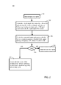
- FIG. 2 is a block diagram showing a method for generating a divided clock signal having a 50% duty cycle in accordance with an embodiment of the present invention.
- FIG. 3 is an illustration of a frequency divider having duty cycle correction logic that includes an AND gate in accordance with an embodiment of the present invention.
- FIG. 4 is a waveform diagram showing signals generated by an embodiment in which N is 25 in accordance with an embodiment of the present invention.
- FIG. 5 is an illustration of a frequency divider having duty cycle correction logic that includes an OR gate in accordance with an embodiment of the present invention.
- Frequency divider 10 includes adder 2 and a multiplexer 3 that is electrically coupled to adder 2 .
- Adder 2 has a first input for receiving a first value M and a second input for receiving a least significant bit (LSB) and is operable to generate a second value at the output of the adder that is the sum of the first value M and the LSB.
- Adder 2 can be synthesized by standard logic cells that calculate MSB+LSB and store the value M+LSB as one of the inputs of multiplexer 3 . In the present embodiment, after calculating M+LSB, adder 2 remains idle to reduce power consumption and only recalculates if the divisor changes.
- Multiplexer 3 has a first input terminal coupled to receive the first value M (first value) and having a second input terminal electrically coupled to the output of the adder for receiving M+LSB (the second value) and is operable in response to input at a select terminal to alternately output the first value M and the second value M+LSB.
- Frequency divider 10 also includes a multi-modulus divider 4 that is electrically coupled to multiplexer 3 for receiving the output of multiplexer 3 .
- Multi-modulus divider 4 includes a clock input for receiving an input clock signal Clk in signal and an input for receiving the complement of the input clock signal.
- Multi-modulus divider 4 can be a conventional high-speed programmable integer-N divider such as, for example, a simple loadable digital counter that is operable to alternately generate an output pulse at M input clock cycles and at M+LSB cycles of the reference clock signal Clk in .
- Multi-modulus divider 4 does not include complex half-cycle counting circuitry or duty cycle correction circuitry, providing for fast and efficient generation of output pulses having a desired frequency.
- Divide-by-two counter 5 has an input coupled to the output of the multi-modulus divider 4 and is operable to divide the output of multi-modulus divider 4 to generate a divided clock signal Clk 1 having a frequency of N, where N is equal to 2M+LSB.
- the output of the divide-by-2 counter is electrically coupled to the select terminal of multiplexer 3 such that multiplexer 3 receives the divided clock signal Clk 1 for controlling the operation of multiplexer 3 .
- Duty cycle correction logic 6 is electrically coupled to the output of divide-by-two counter 5 and receives as input the input clock signal, the complement of the input clock signal and the LSB. Duty cycle correction logic 6 is configured to correct the duty cycle of the divided clock signal to a fifty percent duty cycle when N is odd to generate an output clock signal Clk out .
- FIG. 2 illustrates a method 100 for generating a divided clock signal having a 50% duty cycle that includes receiving 101 an input clock signal and alternately dividing 102 the input clock signal by a divisor M and a divisor M plus a least significant bit (LSB) to alternate periodically between generating an output pulse at M input clock cycles and M+LSB input clock cycles.
- LSB least significant bit
- the divided clock signal has an output that is high for M+1 cycles and low for M cycles.
- the duty cycle of the divided clock signal is corrected 104 - 105 by duty-cycle-correction-logic 6 when the LSB is odd to generate a corrected divided clock signal having a fifty percent duty cycle.
- the divided clock signal is not corrected and becomes the output clock signal as shown by steps 104 and 106 .
- divide-by-two counter 5 further comprises a flip-flop 22 and an inverter 21 coupled to the flip-flop 22 .
- Inverter 21 has an input coupled to receive the divided clock signal Clk 1 and has an output coupled to the D input of flip-flop 22 .
- Flip-flop 22 has a clock input coupled to receive the output of the multi-modulus divider 4 , the flip-flop 22 operable to generate the divided clock signal Clk 1 .
- flip-flop 22 will produce a divided clock signal having a 50% duty cycle when N is even and an output having a near-50% duty cycle when N is odd. More particularly, when N is odd the output will have a pulse width that is slightly larger than 50% because the output is high for M+1 input cycles and low for M input cycles.
- duty cycle correction logic 6 includes AND gate 25 , a first flip-flop 23 and a second flip-flop 24 .
- the output of flip-flop 22 is electrically coupled to the D input of flip-flop 23 and the output of first flip-flop 23 is coupled to a first input of AND gate 25 and a reset terminal of flip-flop 24 is electrically coupled to receive the LSB.
- the complement of the output of the first flip-flop 23 is coupled to a D input of second flip-flop 24 and the complement of the output of second flip-flop 24 is electrically coupled to the second input of the AND gate 25 .
- Flip-flop 23 is clocked by the input clock signal Clk in and flip-flop 24 is clocked by the complement of the input clock signal such that flip-flops 23 - 24 are clocked at a half an input period apart from each other.
- flip-flop 23 and flip-flop 24 that can be D-type flip-flops are operable for coupling their outputs that are half of a clock cycle apart from each other to AND gate 25 so as to generate an output clock signal having the desired 50% duty cycle.
- Flip-flop 23 generates output Q 43 and flip-flop 24 generates a corresponding output 44 that is coupled to AND gate 25 so as to generate output signal 45 at the output of AND gate 25 having the required 50% duty cycle.
- a programmable frequency divider 10 b that includes an OR gate 55 . More particularly, the output of first flip-flop 23 is coupled to a first input of OR gate 55 and to the D-input of second flip-flop 24 . The output of second flip-flop 24 is electrically coupled to the second input of the OR gate 55 . As in the previous embodiment, flip-flop 23 is clocked by the input clock signal Clk in and flip-flop 24 is clocked by the complement of the input clock signal such that flip-flops 23 - 24 are clocked at a half an input period apart from each other.
- the method and apparatus of the present invention provides a frequency divider having a simplified architecture that does not require counting in half-cycles as do conventional programmable frequency dividers. More particularly, multi-modulus divider 4 and divide-by-two counter 5 operate on full clock cycles, and therefore have a simplified architecture as compared to corresponding structures of frequency dividers that require counting in half cycles. Accordingly, the frequency divider 10 of the present invention provides for reduced die area and lower power consumption than conventional frequency dividers that require counting in half cycles. Moreover, by not requiring counting in half cycles, the method and apparatus of the present invention allows for higher speed operation.
- frequency divider 10 , 10 a , 10 b are an Application-Specific Integrated Circuit (ASIC) devices formed on a single semiconductor die. Accordingly, adder 2 , multiplexer 3 , multi-modulus divider 4 , divide-by-two counter 5 and duty cycle correction logic 6 are disposed on a single semiconductor die.
- ASIC Application-Specific Integrated Circuit
- the methods and apparatus of the present invention may be implemented in a Field Programmable Gate Array (FPGA), an Application-Specific Integrated Circuit (ASIC) or a variety of other commonly known integrated circuit devices.
- FPGA Field Programmable Gate Array
- ASIC Application-Specific Integrated Circuit
- the implementation of the invention may include both hardware and software components.
Abstract
Description
Claims (18)
Priority Applications (1)
| Application Number | Priority Date | Filing Date | Title |
|---|---|---|---|
| US14/839,817 US9590637B1 (en) | 2015-08-28 | 2015-08-28 | High-speed programmable frequency divider with 50% output duty cycle |
Applications Claiming Priority (1)
| Application Number | Priority Date | Filing Date | Title |
|---|---|---|---|
| US14/839,817 US9590637B1 (en) | 2015-08-28 | 2015-08-28 | High-speed programmable frequency divider with 50% output duty cycle |
Publications (1)
| Publication Number | Publication Date |
|---|---|
| US9590637B1 true US9590637B1 (en) | 2017-03-07 |
Family
ID=58162327
Family Applications (1)
| Application Number | Title | Priority Date | Filing Date |
|---|---|---|---|
| US14/839,817 Active US9590637B1 (en) | 2015-08-28 | 2015-08-28 | High-speed programmable frequency divider with 50% output duty cycle |
Country Status (1)
| Country | Link |
|---|---|
| US (1) | US9590637B1 (en) |
Cited By (2)
| Publication number | Priority date | Publication date | Assignee | Title |
|---|---|---|---|---|
| CN111092617A (en) * | 2018-10-23 | 2020-05-01 | 台湾积体电路制造股份有限公司 | Frequency divider circuit |
| US10972112B1 (en) * | 2019-11-25 | 2021-04-06 | Shanghai Huali Microelectronics Corporation | 50%-duty-cycle consecutive integer frequency divider and phase-locked loop circuit |
Citations (110)
| Publication number | Priority date | Publication date | Assignee | Title |
|---|---|---|---|---|
| US4862485A (en) | 1987-10-14 | 1989-08-29 | National Semiconductor Corporation | Quotient phase-shift processor for digital phase-locked-loops |
| US5663105A (en) | 1994-05-02 | 1997-09-02 | Texas Instruments Incorporated | Semiconductor device package side-by-side stacking and mounting system |
| US5748949A (en) * | 1996-07-02 | 1998-05-05 | Motorola Inc. | Counter having programmable periods and method therefor |
| US5757240A (en) | 1996-07-01 | 1998-05-26 | International Business Machines Corporation | Low gain voltage-controlled oscillator |
| US5903195A (en) | 1998-01-30 | 1999-05-11 | International Business Machines Corporation | Automatically ranging phase locked loop circuit for microprocessor clock generation |
| US6219797B1 (en) | 1993-02-09 | 2001-04-17 | Dallas Semiconductor Corporation | Microcontroller with selectable oscillator source |
| US6259327B1 (en) | 1998-12-11 | 2001-07-10 | Cselt - Centro Studi E Laboratori Telecomunicazioni S.P.A. | PLL having circuits for selecting optimum VCO input/output characteristics |
| US20020079937A1 (en) | 2000-09-05 | 2002-06-27 | Thucydides Xanthopoulos | Digital delay locked loop with wide dynamic range and fine precision |
| US20020191727A1 (en) | 2001-04-25 | 2002-12-19 | Texas Instruments Incorporated | Digital phase locked loop |
| US20030042985A1 (en) | 2001-08-30 | 2003-03-06 | Hitachi, Ltd. | Phase synchronizing circuit |
| US20030184350A1 (en) * | 2002-03-28 | 2003-10-02 | Elan Microelectronics Corp. | Device for programmable frequency divider |
| US6640311B1 (en) | 2000-08-10 | 2003-10-28 | Bae Systems Information And Electronic Systems Integration, Inc. | Redundant oscillator and method for generating a regulated signal |
| US6643787B1 (en) | 1999-10-19 | 2003-11-04 | Rambus Inc. | Bus system optimization |
| US6650193B2 (en) | 2001-04-06 | 2003-11-18 | Seiko Epson Corporation | Oscillator with a noise reduction function, a writer, and a method of controlling a writer |
| US6683506B2 (en) | 2002-01-18 | 2004-01-27 | The Regents Of The University Of California | CMOS phase locked loop with voltage controlled oscillator having realignment to reference and method for the same |
| US6727767B2 (en) | 2001-09-28 | 2004-04-27 | Seiko Epson Corp | Voltage controlled oscillator with two layered mounting structure |
| US20040136440A1 (en) | 2002-12-24 | 2004-07-15 | Fujitsu Limited | Spread spectrum clock generation circuit, jitter generation circuit and semiconductor device |
| US6768387B1 (en) | 2000-03-08 | 2004-07-27 | Renesas Technology Corporation | Voltage controlled oscillator and PLL circuit using the same |
| US20040165691A1 (en) | 2003-02-25 | 2004-08-26 | Rana Ram Singh | Fractional-N synthesizer with two control words |
| US7012476B2 (en) | 2003-03-20 | 2006-03-14 | Seiko Epson Corporation | Voltage-controlled oscillator, clock converter, and electronic device |
| US20060103436A1 (en) | 2004-11-17 | 2006-05-18 | Fujitsu Limited | Reset control circuit and reset control method |
| US20060119402A1 (en) | 2003-05-02 | 2006-06-08 | Axel Thomsen | Multi-frequency clock synthesizer |
| US20060197614A1 (en) | 2005-03-01 | 2006-09-07 | Regis Roubadia | Multi-phase realigned voltage-controlled oscillator and phase-locked loop incorporating the same |
| US20060290391A1 (en) | 2005-06-27 | 2006-12-28 | Lsi Logic Corporation | Integrated clock generator with programmable spread spectrum using standard PLL circuitry |
| US20070149144A1 (en) | 2005-12-17 | 2007-06-28 | Atmel Germany Gmbh | PLL frequency generator |
| US20070247248A1 (en) | 2006-04-19 | 2007-10-25 | Kabushiki Kaisha Toshiba | Controller for oscillator |
| US7323916B1 (en) | 2005-12-07 | 2008-01-29 | Netlogic Microsystems, Inc. | Methods and apparatus for generating multiple clocks using feedback interpolation |
| US20080043893A1 (en) | 2006-08-18 | 2008-02-21 | Krishnaswamy Nagaraj | Loop bandwidth enhancement technique for a digital PLL and a HF divider that enables this technique |
| US20080104435A1 (en) | 2004-03-22 | 2008-05-01 | Mobius Microsystems, Inc. | Clock Generator, Timing and Frequency Reference with Crystal-Compatible Power Management |
| US20080129351A1 (en) | 2006-05-15 | 2008-06-05 | Stmicroelectronics Pvt. Ltd. | Spread spectrum clock generation |
| US7405594B1 (en) | 2006-06-16 | 2008-07-29 | Integrated Device Technology, Inc. | Current mode driver with constant voltage swing |
| US7434083B1 (en) | 2004-01-06 | 2008-10-07 | Apple Inc. | Method and apparatus for the generation and control of clock signals |
| US20080246546A1 (en) | 2007-04-04 | 2008-10-09 | Samsung Electronics Co., Ltd. | Phase-Locked-Loop Circuit Having a Pre-Calibration Function and Method of Pre-Calibrating the Same |
| US20090083567A1 (en) | 2007-01-31 | 2009-03-26 | Korea University Industrial & Academic Collaboration Foundation | Apparatus and method for clock generation with piecewise linear modulation |
| US7541848B1 (en) | 2007-12-25 | 2009-06-02 | Hitachi, Ltd. | PLL circuit |
| US20090140896A1 (en) | 2007-11-23 | 2009-06-04 | Stmicroelectronics S.R.L. | Clock dithering process for reducing electromagnetic interference in d/a converters and apparatus for carrying out such process |
| US7545188B1 (en) | 2006-08-04 | 2009-06-09 | Integrated Device Technology, Inc | Multiphase clock generator |
| US20090153252A1 (en) | 2007-12-13 | 2009-06-18 | Mei-Show Chen | Multi-band voltage controlled oscillator controlling module, phase locked loop utilizing which and related method thereof |
| US20090184857A1 (en) | 2008-01-07 | 2009-07-23 | Kabushiki Kaisha Toshiba | A/d converting apparatus |
| US7573303B1 (en) | 2007-06-08 | 2009-08-11 | Integrated Device Technology, Inc | Digitally controlled system on-chip (SOC) clock generator |
| US7586347B1 (en) | 2007-09-27 | 2009-09-08 | Integrated Device Technology, Inc. | Clock generator with self-bias bandwidth control |
| US7590163B1 (en) | 2006-05-19 | 2009-09-15 | Conexant Systems, Inc. | Spread spectrum clock generation |
| US20090231901A1 (en) | 2008-03-11 | 2009-09-17 | Hynix Semiconductor, Inc. | Semiconductor integrated circuit for supporting a test mode |
| US20090256601A1 (en) | 2008-04-14 | 2009-10-15 | Qualcomm Incorporated | Phase to digital converter in all digital phase locked loop |
| US20090262567A1 (en) | 2008-04-16 | 2009-10-22 | Shin Chang-Hee | Nonvolatile memory device |
| US20100007427A1 (en) | 2007-03-21 | 2010-01-14 | Fujitsu Microelectronics Limited | Switching capacitor generation circuit |
| US7671635B2 (en) | 2007-09-12 | 2010-03-02 | National Taiwan University | Frequency synthesizer, coupled divide-by-N circuit, current-reuse multiply-by-M circuit |
| US20100052798A1 (en) | 2008-09-02 | 2010-03-04 | Nec Electronics Corporation | Phase-locked loop circuit |
| US20100090731A1 (en) | 2008-10-03 | 2010-04-15 | The Swatch Group Research And Development Ltd. | Self-calibration method for a frequency synthesizer using two point fsk modulation |
| US7737739B1 (en) | 2007-12-12 | 2010-06-15 | Integrated Device Technology, Inc. | Phase step clock generator |
| US7741981B1 (en) | 2008-12-30 | 2010-06-22 | Hong Kong Applied Science And Technology Research Institute Co., Ltd. | Dual-use comparator/op amp for use as both a successive-approximation ADC and DAC |
| US7750618B1 (en) | 2006-07-25 | 2010-07-06 | Integrated Device Technology, Inc. | System and method for testing a clock circuit |
| US20100194483A1 (en) | 2009-02-05 | 2010-08-05 | International Business Machines Corporation | Auto-calibration for ring oscillator vco |
| US7786763B1 (en) | 2008-12-30 | 2010-08-31 | Integrated Device Technology, Inc. | Clock circuit with harmonic frequency detector |
| US20100240323A1 (en) | 2009-03-19 | 2010-09-23 | Qualcomm Incorporated | Frequency divider with synchronized outputs |
| US7816959B1 (en) | 2009-02-23 | 2010-10-19 | Integrated Device Technology, Inc. | Clock circuit for reducing long term jitter |
| US20100323643A1 (en) | 2008-02-28 | 2010-12-23 | Nxp B.V. | Frequency synthesis |
| US20110006936A1 (en) | 2009-07-09 | 2011-01-13 | National Taiwan University | All-digital spread spectrum clock generator |
| US20110032013A1 (en) | 2010-07-19 | 2011-02-10 | Analog Devices, Inc. | Digital Phase-Locked Loop Clock System |
| US7907625B1 (en) | 2008-08-04 | 2011-03-15 | Integrated Device Technology, Inc. | Power reduction technique for buffered crossbar switch |
| US7928880B2 (en) | 2008-08-18 | 2011-04-19 | Fujitsu Limited | Digital analog converter |
| US20110095784A1 (en) | 2009-10-26 | 2011-04-28 | Analog Devices, Inc. | Apparatus and method for providing multi-mode clock signals |
| US7941723B1 (en) | 2007-09-26 | 2011-05-10 | Integrated Device Technology, Inc. | Clock generator and method for providing reliable clock signal using array of MEMS resonators |
| US8018289B1 (en) | 2009-08-19 | 2011-09-13 | Integrated Device Technology, Inc. | Holdover circuit for phase-lock loop |
| US20110234433A1 (en) | 2010-03-24 | 2011-09-29 | Fujitsu Semiconductor Limited | A/d converter |
| US20110234204A1 (en) | 2010-03-25 | 2011-09-29 | Fujitsu Limited | Radio-frequency power amplifier |
| US20110285575A1 (en) | 2009-02-13 | 2011-11-24 | Freescale Semiconductor, Inc. | Integrated circuit comprising frequency generation circuitry for controlling a frequency source |
| US20110304490A1 (en) | 2010-06-11 | 2011-12-15 | Texas Instruments Incorporated | Low power comparator for use in sar adcs |
| US20120013406A1 (en) | 2010-07-19 | 2012-01-19 | Analog Devices, Inc. | Digital phase-locked loop clock system |
| US8164367B1 (en) | 2009-01-15 | 2012-04-24 | Integrated Device Technology, Inc. | Spread spectrum clock generation technique for imaging applications |
| US8179952B2 (en) | 2008-05-23 | 2012-05-15 | Integrated Device Technology Inc. | Programmable duty cycle distortion generation circuit |
| US20120161829A1 (en) | 2010-12-22 | 2012-06-28 | Fernald Kenneth W | Frequency locked loop |
| US20120200330A1 (en) | 2011-02-09 | 2012-08-09 | Lapis Semiconductor Co., Ltd. | Semiconductor integrated circuit, semiconductor chip and method of designing semiconductor integrated circuit |
| US8259888B2 (en) | 2008-05-23 | 2012-09-04 | Integrated Device Technology, Inc. | Method of processing signal data with corrected clock phase offset |
| US20120249207A1 (en) | 2011-03-30 | 2012-10-04 | Kenichi Natsume | Clock signal generation circuit |
| US8284816B1 (en) | 2009-06-01 | 2012-10-09 | Integrated Device Technology, Inc. | Push-pull spread spectrum clock signal generator |
| US20120262315A1 (en) | 2011-04-13 | 2012-10-18 | Analog Devices, Inc. | Self-timed digital-to-analog converter |
| US8305154B1 (en) | 2010-07-13 | 2012-11-06 | Hrl Laboratories, Llc | Parametrically driven quartz UHF oscillator |
| US20120297231A1 (en) | 2011-05-19 | 2012-11-22 | Shekoufeh Qawami | Interface for Storage Device Access Over Memory Bus |
| US20120317365A1 (en) | 2011-06-07 | 2012-12-13 | Sandisk Technologies Inc. | System and method to buffer data |
| US20120328052A1 (en) | 2011-06-22 | 2012-12-27 | Broadcom Corporation | Spur Mitigation For Radio Frequency Receivers Utilizing A Free-Running Crystal |
| US20130002467A1 (en) | 2011-06-30 | 2013-01-03 | Zhenning Wang | Two-stage analog-to-digital converter using sar and tdc |
| US8416107B1 (en) | 2011-09-28 | 2013-04-09 | Hong Kong Applied Science & Technology Research Institute Company Ltd. | Charge compensation calibration for high resolution data converter |
| US8436677B2 (en) | 2010-12-13 | 2013-05-07 | International Business Machines Corporation | Structure for a reference voltage generator for analog to digital converters |
| US20130162454A1 (en) | 2011-12-21 | 2013-06-27 | Realtek Semiconductor Corp. | High-speed successive-approximation-register analog-to-digital converter and method thereof |
| US20130194115A1 (en) | 2012-01-31 | 2013-08-01 | Qiong Wu | Successive approximation register analog to digital converter |
| US20130211758A1 (en) | 2012-02-15 | 2013-08-15 | Texas Instruments Incorporated | Reference clock re-timing scheme in electronic circuits |
| US8537952B1 (en) | 2007-03-08 | 2013-09-17 | Marvell International Ltd. | Fractional-N frequency synthesizer with separate phase and frequency detectors |
| US20130300455A1 (en) | 2012-05-11 | 2013-11-14 | Rajesh Thirugnanam | Multiple signal format output driver with configurable internal load |
| US20140029646A1 (en) | 2012-07-27 | 2014-01-30 | Ati Technologies Ulc | Disabling spread-spectrum clock signal generation |
| US8693557B1 (en) | 2009-07-02 | 2014-04-08 | Integrated Device Technology Inc. | AC coupled clock receiver with common-mode noise rejection |
| US8704564B2 (en) | 2012-04-16 | 2014-04-22 | Fujitsu Semiconductor Limited | PLL circuit |
| US8723573B1 (en) | 2012-06-20 | 2014-05-13 | Integrated Device Technology, Inc. | Method and apparatus for reducing crowbar current and controlling slew rate |
| US8791763B2 (en) | 2012-08-09 | 2014-07-29 | Qualcomm Incorporated | Tunable injection locked dividers with enhanced locking range |
| US20140210532A1 (en) | 2013-01-29 | 2014-07-31 | Perceptia Devices Australia Pty Ltd. | Phase-Locked Loop Apparatus and Method |
| US20140327478A1 (en) | 2013-05-06 | 2014-11-06 | National Sun Yat-Sen University | Wideband frequency synthesizer and frequency synthesizing method thereof |
| US8896476B2 (en) | 2013-01-25 | 2014-11-25 | Technische Universiteit Eindhoven | Data-driven noise reduction technique for analog to digital converters |
| US20140347941A1 (en) | 2013-05-24 | 2014-11-27 | Qualcomm Incorporated | Low latency synchronization scheme for mesochronous ddr system |
| US8933830B1 (en) | 2013-07-24 | 2015-01-13 | Electronics And Telecommunications Research Institute | Successive approximation register analog-to-digital converter and method of operating built-in self-test device for testing the converter |
| US8981858B1 (en) | 2011-12-30 | 2015-03-17 | Cypress Semiconductor Corporation | Spread spectrum oscillator |
| US20150162921A1 (en) | 2013-12-05 | 2015-06-11 | Taiwan Semiconductor Manufacturing Company, Ltd. | Circuit and operating method of pll |
| US20150180594A1 (en) | 2013-12-20 | 2015-06-25 | Texas Instruments Deutschland Gmbh | Self-calibrating shared-component dual synthesizer |
| US9077386B1 (en) | 2010-05-20 | 2015-07-07 | Kandou Labs, S.A. | Methods and systems for selection of unions of vector signaling codes for power and pin efficient chip-to-chip communication |
| US20150200649A1 (en) | 2014-01-10 | 2015-07-16 | Silicon Laboratories Inc. | Frequency management using sample rate conversion |
| US20150213873A1 (en) | 2014-01-28 | 2015-07-30 | Samsung Electronics Co., Ltd. | Injection-locked phase locked loop circuits using delay locked loops |
| US9100232B1 (en) | 2014-02-02 | 2015-08-04 | Kandou Labs, S.A. | Method for code evaluation using ISI ratio |
| US20160084895A1 (en) | 2014-09-18 | 2016-03-24 | Fluke Corporation | Detecting, localizing and ranking copper connectors |
| US20160119118A1 (en) | 2014-10-22 | 2016-04-28 | Kandou Labs, S.A. | Method and apparatus for high speed chip-to-chip communications |
| US20160162426A1 (en) | 2014-12-05 | 2016-06-09 | Marvell Israel (M.I.S.L) Ltd. | Optimal sampling of data-bus signals using configurable individual time delays |
| US9455854B2 (en) | 2014-06-03 | 2016-09-27 | Huawei Technologies Co., Ltd. | Phase-locked loop frequency calibration method and system |
-
2015
- 2015-08-28 US US14/839,817 patent/US9590637B1/en active Active
Patent Citations (118)
| Publication number | Priority date | Publication date | Assignee | Title |
|---|---|---|---|---|
| US4862485A (en) | 1987-10-14 | 1989-08-29 | National Semiconductor Corporation | Quotient phase-shift processor for digital phase-locked-loops |
| US6219797B1 (en) | 1993-02-09 | 2001-04-17 | Dallas Semiconductor Corporation | Microcontroller with selectable oscillator source |
| US5663105A (en) | 1994-05-02 | 1997-09-02 | Texas Instruments Incorporated | Semiconductor device package side-by-side stacking and mounting system |
| US5757240A (en) | 1996-07-01 | 1998-05-26 | International Business Machines Corporation | Low gain voltage-controlled oscillator |
| US5748949A (en) * | 1996-07-02 | 1998-05-05 | Motorola Inc. | Counter having programmable periods and method therefor |
| US5903195A (en) | 1998-01-30 | 1999-05-11 | International Business Machines Corporation | Automatically ranging phase locked loop circuit for microprocessor clock generation |
| US6259327B1 (en) | 1998-12-11 | 2001-07-10 | Cselt - Centro Studi E Laboratori Telecomunicazioni S.P.A. | PLL having circuits for selecting optimum VCO input/output characteristics |
| US6643787B1 (en) | 1999-10-19 | 2003-11-04 | Rambus Inc. | Bus system optimization |
| US6768387B1 (en) | 2000-03-08 | 2004-07-27 | Renesas Technology Corporation | Voltage controlled oscillator and PLL circuit using the same |
| US6640311B1 (en) | 2000-08-10 | 2003-10-28 | Bae Systems Information And Electronic Systems Integration, Inc. | Redundant oscillator and method for generating a regulated signal |
| US20020079937A1 (en) | 2000-09-05 | 2002-06-27 | Thucydides Xanthopoulos | Digital delay locked loop with wide dynamic range and fine precision |
| US6650193B2 (en) | 2001-04-06 | 2003-11-18 | Seiko Epson Corporation | Oscillator with a noise reduction function, a writer, and a method of controlling a writer |
| US20020191727A1 (en) | 2001-04-25 | 2002-12-19 | Texas Instruments Incorporated | Digital phase locked loop |
| US20030042985A1 (en) | 2001-08-30 | 2003-03-06 | Hitachi, Ltd. | Phase synchronizing circuit |
| US6870411B2 (en) | 2001-08-30 | 2005-03-22 | Renesas Technology Corp. | Phase synchronizing circuit |
| US6727767B2 (en) | 2001-09-28 | 2004-04-27 | Seiko Epson Corp | Voltage controlled oscillator with two layered mounting structure |
| US6683506B2 (en) | 2002-01-18 | 2004-01-27 | The Regents Of The University Of California | CMOS phase locked loop with voltage controlled oscillator having realignment to reference and method for the same |
| US20030184350A1 (en) * | 2002-03-28 | 2003-10-02 | Elan Microelectronics Corp. | Device for programmable frequency divider |
| US6959066B2 (en) * | 2002-03-28 | 2005-10-25 | Elan Microelectronics Corp. | Device for programmable frequency divider |
| US20040136440A1 (en) | 2002-12-24 | 2004-07-15 | Fujitsu Limited | Spread spectrum clock generation circuit, jitter generation circuit and semiconductor device |
| US20040165691A1 (en) | 2003-02-25 | 2004-08-26 | Rana Ram Singh | Fractional-N synthesizer with two control words |
| US7012476B2 (en) | 2003-03-20 | 2006-03-14 | Seiko Epson Corporation | Voltage-controlled oscillator, clock converter, and electronic device |
| US20060119402A1 (en) | 2003-05-02 | 2006-06-08 | Axel Thomsen | Multi-frequency clock synthesizer |
| US7434083B1 (en) | 2004-01-06 | 2008-10-07 | Apple Inc. | Method and apparatus for the generation and control of clock signals |
| US20080104435A1 (en) | 2004-03-22 | 2008-05-01 | Mobius Microsystems, Inc. | Clock Generator, Timing and Frequency Reference with Crystal-Compatible Power Management |
| US20060103436A1 (en) | 2004-11-17 | 2006-05-18 | Fujitsu Limited | Reset control circuit and reset control method |
| US20060197614A1 (en) | 2005-03-01 | 2006-09-07 | Regis Roubadia | Multi-phase realigned voltage-controlled oscillator and phase-locked loop incorporating the same |
| US20060290391A1 (en) | 2005-06-27 | 2006-12-28 | Lsi Logic Corporation | Integrated clock generator with programmable spread spectrum using standard PLL circuitry |
| US7323916B1 (en) | 2005-12-07 | 2008-01-29 | Netlogic Microsystems, Inc. | Methods and apparatus for generating multiple clocks using feedback interpolation |
| US20070149144A1 (en) | 2005-12-17 | 2007-06-28 | Atmel Germany Gmbh | PLL frequency generator |
| US20070247248A1 (en) | 2006-04-19 | 2007-10-25 | Kabushiki Kaisha Toshiba | Controller for oscillator |
| US20080129351A1 (en) | 2006-05-15 | 2008-06-05 | Stmicroelectronics Pvt. Ltd. | Spread spectrum clock generation |
| US7590163B1 (en) | 2006-05-19 | 2009-09-15 | Conexant Systems, Inc. | Spread spectrum clock generation |
| US7405594B1 (en) | 2006-06-16 | 2008-07-29 | Integrated Device Technology, Inc. | Current mode driver with constant voltage swing |
| US7750618B1 (en) | 2006-07-25 | 2010-07-06 | Integrated Device Technology, Inc. | System and method for testing a clock circuit |
| US7545188B1 (en) | 2006-08-04 | 2009-06-09 | Integrated Device Technology, Inc | Multiphase clock generator |
| US20080043893A1 (en) | 2006-08-18 | 2008-02-21 | Krishnaswamy Nagaraj | Loop bandwidth enhancement technique for a digital PLL and a HF divider that enables this technique |
| US20090083567A1 (en) | 2007-01-31 | 2009-03-26 | Korea University Industrial & Academic Collaboration Foundation | Apparatus and method for clock generation with piecewise linear modulation |
| US8537952B1 (en) | 2007-03-08 | 2013-09-17 | Marvell International Ltd. | Fractional-N frequency synthesizer with separate phase and frequency detectors |
| US20100007427A1 (en) | 2007-03-21 | 2010-01-14 | Fujitsu Microelectronics Limited | Switching capacitor generation circuit |
| US20080246546A1 (en) | 2007-04-04 | 2008-10-09 | Samsung Electronics Co., Ltd. | Phase-Locked-Loop Circuit Having a Pre-Calibration Function and Method of Pre-Calibrating the Same |
| US7573303B1 (en) | 2007-06-08 | 2009-08-11 | Integrated Device Technology, Inc | Digitally controlled system on-chip (SOC) clock generator |
| US7671635B2 (en) | 2007-09-12 | 2010-03-02 | National Taiwan University | Frequency synthesizer, coupled divide-by-N circuit, current-reuse multiply-by-M circuit |
| US7941723B1 (en) | 2007-09-26 | 2011-05-10 | Integrated Device Technology, Inc. | Clock generator and method for providing reliable clock signal using array of MEMS resonators |
| US7586347B1 (en) | 2007-09-27 | 2009-09-08 | Integrated Device Technology, Inc. | Clock generator with self-bias bandwidth control |
| US20090140896A1 (en) | 2007-11-23 | 2009-06-04 | Stmicroelectronics S.R.L. | Clock dithering process for reducing electromagnetic interference in d/a converters and apparatus for carrying out such process |
| US7737739B1 (en) | 2007-12-12 | 2010-06-15 | Integrated Device Technology, Inc. | Phase step clock generator |
| US20090153252A1 (en) | 2007-12-13 | 2009-06-18 | Mei-Show Chen | Multi-band voltage controlled oscillator controlling module, phase locked loop utilizing which and related method thereof |
| US7541848B1 (en) | 2007-12-25 | 2009-06-02 | Hitachi, Ltd. | PLL circuit |
| US20090184857A1 (en) | 2008-01-07 | 2009-07-23 | Kabushiki Kaisha Toshiba | A/d converting apparatus |
| US20100323643A1 (en) | 2008-02-28 | 2010-12-23 | Nxp B.V. | Frequency synthesis |
| US20090231901A1 (en) | 2008-03-11 | 2009-09-17 | Hynix Semiconductor, Inc. | Semiconductor integrated circuit for supporting a test mode |
| US20090256601A1 (en) | 2008-04-14 | 2009-10-15 | Qualcomm Incorporated | Phase to digital converter in all digital phase locked loop |
| US20090262567A1 (en) | 2008-04-16 | 2009-10-22 | Shin Chang-Hee | Nonvolatile memory device |
| US8259888B2 (en) | 2008-05-23 | 2012-09-04 | Integrated Device Technology, Inc. | Method of processing signal data with corrected clock phase offset |
| US8179952B2 (en) | 2008-05-23 | 2012-05-15 | Integrated Device Technology Inc. | Programmable duty cycle distortion generation circuit |
| US7907625B1 (en) | 2008-08-04 | 2011-03-15 | Integrated Device Technology, Inc. | Power reduction technique for buffered crossbar switch |
| US7928880B2 (en) | 2008-08-18 | 2011-04-19 | Fujitsu Limited | Digital analog converter |
| US20100052798A1 (en) | 2008-09-02 | 2010-03-04 | Nec Electronics Corporation | Phase-locked loop circuit |
| US20100090731A1 (en) | 2008-10-03 | 2010-04-15 | The Swatch Group Research And Development Ltd. | Self-calibration method for a frequency synthesizer using two point fsk modulation |
| US7786763B1 (en) | 2008-12-30 | 2010-08-31 | Integrated Device Technology, Inc. | Clock circuit with harmonic frequency detector |
| US20100164761A1 (en) | 2008-12-30 | 2010-07-01 | Hong Kong Applied Science & Technology Research Institute Company Limited | Dual-use comparator/op amp for use as both a successive-approximation adc and dac |
| US7741981B1 (en) | 2008-12-30 | 2010-06-22 | Hong Kong Applied Science And Technology Research Institute Co., Ltd. | Dual-use comparator/op amp for use as both a successive-approximation ADC and DAC |
| US8164367B1 (en) | 2009-01-15 | 2012-04-24 | Integrated Device Technology, Inc. | Spread spectrum clock generation technique for imaging applications |
| US20100194483A1 (en) | 2009-02-05 | 2010-08-05 | International Business Machines Corporation | Auto-calibration for ring oscillator vco |
| US20110285575A1 (en) | 2009-02-13 | 2011-11-24 | Freescale Semiconductor, Inc. | Integrated circuit comprising frequency generation circuitry for controlling a frequency source |
| US7816959B1 (en) | 2009-02-23 | 2010-10-19 | Integrated Device Technology, Inc. | Clock circuit for reducing long term jitter |
| US20100240323A1 (en) | 2009-03-19 | 2010-09-23 | Qualcomm Incorporated | Frequency divider with synchronized outputs |
| US8284816B1 (en) | 2009-06-01 | 2012-10-09 | Integrated Device Technology, Inc. | Push-pull spread spectrum clock signal generator |
| US8693557B1 (en) | 2009-07-02 | 2014-04-08 | Integrated Device Technology Inc. | AC coupled clock receiver with common-mode noise rejection |
| US20110006936A1 (en) | 2009-07-09 | 2011-01-13 | National Taiwan University | All-digital spread spectrum clock generator |
| US8018289B1 (en) | 2009-08-19 | 2011-09-13 | Integrated Device Technology, Inc. | Holdover circuit for phase-lock loop |
| US20110095784A1 (en) | 2009-10-26 | 2011-04-28 | Analog Devices, Inc. | Apparatus and method for providing multi-mode clock signals |
| US20110234433A1 (en) | 2010-03-24 | 2011-09-29 | Fujitsu Semiconductor Limited | A/d converter |
| US20110234204A1 (en) | 2010-03-25 | 2011-09-29 | Fujitsu Limited | Radio-frequency power amplifier |
| US8456155B2 (en) | 2010-03-25 | 2013-06-04 | Fujitsu Limited | Radio-frequency power amplifier |
| US9077386B1 (en) | 2010-05-20 | 2015-07-07 | Kandou Labs, S.A. | Methods and systems for selection of unions of vector signaling codes for power and pin efficient chip-to-chip communication |
| US20160211929A1 (en) | 2010-05-20 | 2016-07-21 | Kandou Labs, S.A. | Methods and systems for skew tolerance in and advanced detectors for vector signaling codes for chip-to-chip communication |
| US20110304490A1 (en) | 2010-06-11 | 2011-12-15 | Texas Instruments Incorporated | Low power comparator for use in sar adcs |
| US8305154B1 (en) | 2010-07-13 | 2012-11-06 | Hrl Laboratories, Llc | Parametrically driven quartz UHF oscillator |
| US8188796B2 (en) | 2010-07-19 | 2012-05-29 | Analog Devices, Inc. | Digital phase-locked loop clock system |
| US20120013406A1 (en) | 2010-07-19 | 2012-01-19 | Analog Devices, Inc. | Digital phase-locked loop clock system |
| US20110032013A1 (en) | 2010-07-19 | 2011-02-10 | Analog Devices, Inc. | Digital Phase-Locked Loop Clock System |
| US8432231B2 (en) | 2010-07-19 | 2013-04-30 | Analog Devices, Inc. | Digital phase-locked loop clock system |
| US8436677B2 (en) | 2010-12-13 | 2013-05-07 | International Business Machines Corporation | Structure for a reference voltage generator for analog to digital converters |
| US20120161829A1 (en) | 2010-12-22 | 2012-06-28 | Fernald Kenneth W | Frequency locked loop |
| US20120200330A1 (en) | 2011-02-09 | 2012-08-09 | Lapis Semiconductor Co., Ltd. | Semiconductor integrated circuit, semiconductor chip and method of designing semiconductor integrated circuit |
| US20120249207A1 (en) | 2011-03-30 | 2012-10-04 | Kenichi Natsume | Clock signal generation circuit |
| US20120262315A1 (en) | 2011-04-13 | 2012-10-18 | Analog Devices, Inc. | Self-timed digital-to-analog converter |
| US20120297231A1 (en) | 2011-05-19 | 2012-11-22 | Shekoufeh Qawami | Interface for Storage Device Access Over Memory Bus |
| US20120317365A1 (en) | 2011-06-07 | 2012-12-13 | Sandisk Technologies Inc. | System and method to buffer data |
| US20120328052A1 (en) | 2011-06-22 | 2012-12-27 | Broadcom Corporation | Spur Mitigation For Radio Frequency Receivers Utilizing A Free-Running Crystal |
| US8471751B2 (en) | 2011-06-30 | 2013-06-25 | Intel Corporation | Two-stage analog-to-digital converter using SAR and TDC |
| US20130002467A1 (en) | 2011-06-30 | 2013-01-03 | Zhenning Wang | Two-stage analog-to-digital converter using sar and tdc |
| US8416107B1 (en) | 2011-09-28 | 2013-04-09 | Hong Kong Applied Science & Technology Research Institute Company Ltd. | Charge compensation calibration for high resolution data converter |
| US20130162454A1 (en) | 2011-12-21 | 2013-06-27 | Realtek Semiconductor Corp. | High-speed successive-approximation-register analog-to-digital converter and method thereof |
| US8981858B1 (en) | 2011-12-30 | 2015-03-17 | Cypress Semiconductor Corporation | Spread spectrum oscillator |
| US20130194115A1 (en) | 2012-01-31 | 2013-08-01 | Qiong Wu | Successive approximation register analog to digital converter |
| US20130211758A1 (en) | 2012-02-15 | 2013-08-15 | Texas Instruments Incorporated | Reference clock re-timing scheme in electronic circuits |
| US8704564B2 (en) | 2012-04-16 | 2014-04-22 | Fujitsu Semiconductor Limited | PLL circuit |
| US20130300455A1 (en) | 2012-05-11 | 2013-11-14 | Rajesh Thirugnanam | Multiple signal format output driver with configurable internal load |
| US8723573B1 (en) | 2012-06-20 | 2014-05-13 | Integrated Device Technology, Inc. | Method and apparatus for reducing crowbar current and controlling slew rate |
| US20140029646A1 (en) | 2012-07-27 | 2014-01-30 | Ati Technologies Ulc | Disabling spread-spectrum clock signal generation |
| US8791763B2 (en) | 2012-08-09 | 2014-07-29 | Qualcomm Incorporated | Tunable injection locked dividers with enhanced locking range |
| US8896476B2 (en) | 2013-01-25 | 2014-11-25 | Technische Universiteit Eindhoven | Data-driven noise reduction technique for analog to digital converters |
| US20140210532A1 (en) | 2013-01-29 | 2014-07-31 | Perceptia Devices Australia Pty Ltd. | Phase-Locked Loop Apparatus and Method |
| US20140327478A1 (en) | 2013-05-06 | 2014-11-06 | National Sun Yat-Sen University | Wideband frequency synthesizer and frequency synthesizing method thereof |
| US20140347941A1 (en) | 2013-05-24 | 2014-11-27 | Qualcomm Incorporated | Low latency synchronization scheme for mesochronous ddr system |
| US8933830B1 (en) | 2013-07-24 | 2015-01-13 | Electronics And Telecommunications Research Institute | Successive approximation register analog-to-digital converter and method of operating built-in self-test device for testing the converter |
| US20150162921A1 (en) | 2013-12-05 | 2015-06-11 | Taiwan Semiconductor Manufacturing Company, Ltd. | Circuit and operating method of pll |
| US20150180594A1 (en) | 2013-12-20 | 2015-06-25 | Texas Instruments Deutschland Gmbh | Self-calibrating shared-component dual synthesizer |
| US20150200649A1 (en) | 2014-01-10 | 2015-07-16 | Silicon Laboratories Inc. | Frequency management using sample rate conversion |
| US20150213873A1 (en) | 2014-01-28 | 2015-07-30 | Samsung Electronics Co., Ltd. | Injection-locked phase locked loop circuits using delay locked loops |
| US9100232B1 (en) | 2014-02-02 | 2015-08-04 | Kandou Labs, S.A. | Method for code evaluation using ISI ratio |
| US9455854B2 (en) | 2014-06-03 | 2016-09-27 | Huawei Technologies Co., Ltd. | Phase-locked loop frequency calibration method and system |
| US20160084895A1 (en) | 2014-09-18 | 2016-03-24 | Fluke Corporation | Detecting, localizing and ranking copper connectors |
| US20160119118A1 (en) | 2014-10-22 | 2016-04-28 | Kandou Labs, S.A. | Method and apparatus for high speed chip-to-chip communications |
| US20160162426A1 (en) | 2014-12-05 | 2016-06-09 | Marvell Israel (M.I.S.L) Ltd. | Optimal sampling of data-bus signals using configurable individual time delays |
Non-Patent Citations (9)
| Title |
|---|
| "19-Output PCIE Gen 3 Buffer", Si53019-A01A, Silicon Laboratories Inc., Rev. 1.1 May 2015, 34 Pages. |
| "NB3W1200L: 3.3 V 100/133 MHz Differential 1:12 Push-Pull Clock ZDB/Fanout Buffer for PCIe", ON Semiconductor, http://onsemi.com, Aug. 2013, Rev. 0, 26 Pages. |
| Avramov, et al., "1.5-GHz Voltage Controlled Oscillator with 3% Tuning Bandwidth Using a Two-Pole DSBAR Filter", Ultrasonics, Ferroelectrics and Frequency Control. IEEE Transactions on. vol. 58., May 2011, pp. 916-923. |
| Hwang, et al., "A Digitally Controlled Phase-Locked Loop with a Digital Ohase-Frequency Detector for Fast Acquisition", IEEE Journal of Solid State Circuits, vol. 36, No. 10, Oct. 2001, pp. 1574-1581. |
| Kratyuk, et al., "Frequency Detector for Fast Frequency Lock of Digital PLLs", Electronic Letters, vol. 43, No. 1, Jan. 4, 2007, pp. 1-2. |
| Mansuri, "Fast Frequency Acquisition Phase-Frequency Detectors for GSamples/s Phase-Locked Loops", IEEE Journal of Solid-State Circuits, vol. 37 No. 10, Oct. 2002, pp. 1331-1334. |
| Nagaraju, "A Low Noise 1.5GHz VCO with a 3.75% Tuning Range Using Coupled FBAR's", IEEE International Ultrasonics Symposium (IUS), Oct. 2012, pp. 1-4. |
| Texas Instruments "CDCEx913 Programmable 1-PLL VCXO Clock Synthesizer With 1.8-V, 2.5-V, and 3.3-V Outputs", Apr. 2015, pp. 1-36, pp. 11, 20-22. |
| Watanabe, "An All-Digital PLL for Frequency Multilication by 4 to 1022 with Seven-Cycle Lock Time", IEEE Journal of Solid-State Circuits, vol. 39 No. 2, Feb. 2003, pp. 198-204. |
Cited By (2)
| Publication number | Priority date | Publication date | Assignee | Title |
|---|---|---|---|---|
| CN111092617A (en) * | 2018-10-23 | 2020-05-01 | 台湾积体电路制造股份有限公司 | Frequency divider circuit |
| US10972112B1 (en) * | 2019-11-25 | 2021-04-06 | Shanghai Huali Microelectronics Corporation | 50%-duty-cycle consecutive integer frequency divider and phase-locked loop circuit |
Similar Documents
| Publication | Publication Date | Title |
|---|---|---|
| US7005900B1 (en) | Counter-based clock doubler circuits and methods with optional duty cycle correction and offset | |
| US9008261B2 (en) | Circuits and methods for using a flying-adder synthesizer as a fractional frequency divider | |
| US8471607B1 (en) | High-speed frequency divider architecture | |
| US8704557B2 (en) | High-speed non-integer frequency divider circuit | |
| US8558589B2 (en) | Fully digital method for generating sub clock division and clock waves | |
| US20100253397A1 (en) | Frequency divider circuit | |
| US8644447B2 (en) | System and a method for generating time bases in low power domain | |
| KR100671749B1 (en) | Clock divider | |
| US9590637B1 (en) | High-speed programmable frequency divider with 50% output duty cycle | |
| JP4111932B2 (en) | Clock divider and its trigger signal generation circuit | |
| CN107968646B (en) | Programmable clock divider | |
| JP4977717B2 (en) | Frequency divider circuit | |
| US6956922B2 (en) | Generating non-integer clock division | |
| CN107888166B (en) | Multi-phase non-overlapping clock signal generation circuit and corresponding method | |
| US7323913B1 (en) | Multiphase divider for P-PLL based serial link receivers | |
| CN213585746U (en) | Frequency divider circuit | |
| US9774333B2 (en) | Counter circuit | |
| JP2015139103A (en) | variable frequency divider | |
| US7242231B2 (en) | Programmable fractional-N clock generators | |
| US9160316B2 (en) | Digital controlled oscillator and frequency variable oscillator | |
| TWI469529B (en) | Fractional-n clock generator and method thereof | |
| US9564904B2 (en) | Asynchronous high-speed programmable divider | |
| US7924966B2 (en) | Symmetry corrected high frequency digital divider | |
| TWI462483B (en) | Clock generating circuit and associated method for generating output clock signal | |
| KR101453015B1 (en) | Extended mult-modulus divider |
Legal Events
| Date | Code | Title | Description |
|---|---|---|---|
| AS | Assignment |
Owner name: INTEGRATED DEVICE TECHNOLOGY, INC., CALIFORNIA Free format text: ASSIGNMENT OF ASSIGNORS INTEREST;ASSIGNORS:LAU, PAK-KIM;CHU, MIN;REEL/FRAME:036453/0185 Effective date: 20150827 |
|
| STCF | Information on status: patent grant |
Free format text: PATENTED CASE |
|
| AS | Assignment |
Owner name: JPMORGAN CHASE BANK, N.A., AS COLLATERAL AGENT, NE Free format text: SECURITY AGREEMENT;ASSIGNORS:INTEGRATED DEVICE TECHNOLOGY, INC.;GIGPEAK, INC.;MAGNUM SEMICONDUCTOR, INC.;AND OTHERS;REEL/FRAME:042166/0431 Effective date: 20170404 Owner name: JPMORGAN CHASE BANK, N.A., AS COLLATERAL AGENT, NEW YORK Free format text: SECURITY AGREEMENT;ASSIGNORS:INTEGRATED DEVICE TECHNOLOGY, INC.;GIGPEAK, INC.;MAGNUM SEMICONDUCTOR, INC.;AND OTHERS;REEL/FRAME:042166/0431 Effective date: 20170404 |
|
| AS | Assignment |
Owner name: GIGPEAK, INC., CALIFORNIA Free format text: RELEASE BY SECURED PARTY;ASSIGNOR:JPMORGAN CHASE BANK, N.A.;REEL/FRAME:048746/0001 Effective date: 20190329 Owner name: MAGNUM SEMICONDUCTOR, INC., CALIFORNIA Free format text: RELEASE BY SECURED PARTY;ASSIGNOR:JPMORGAN CHASE BANK, N.A.;REEL/FRAME:048746/0001 Effective date: 20190329 Owner name: INTEGRATED DEVICE TECHNOLOGY, INC., CALIFORNIA Free format text: RELEASE BY SECURED PARTY;ASSIGNOR:JPMORGAN CHASE BANK, N.A.;REEL/FRAME:048746/0001 Effective date: 20190329 Owner name: ENDWAVE CORPORATION, CALIFORNIA Free format text: RELEASE BY SECURED PARTY;ASSIGNOR:JPMORGAN CHASE BANK, N.A.;REEL/FRAME:048746/0001 Effective date: 20190329 Owner name: CHIPX, INCORPORATED, CALIFORNIA Free format text: RELEASE BY SECURED PARTY;ASSIGNOR:JPMORGAN CHASE BANK, N.A.;REEL/FRAME:048746/0001 Effective date: 20190329 |
|
| MAFP | Maintenance fee payment |
Free format text: PAYMENT OF MAINTENANCE FEE, 4TH YEAR, LARGE ENTITY (ORIGINAL EVENT CODE: M1551); ENTITY STATUS OF PATENT OWNER: LARGE ENTITY Year of fee payment: 4 |