US9595656B2 - Double-masking technique for increasing fabrication yield in superconducting electronics - Google Patents
Double-masking technique for increasing fabrication yield in superconducting electronics Download PDFInfo
- Publication number
- US9595656B2 US9595656B2 US14/850,634 US201514850634A US9595656B2 US 9595656 B2 US9595656 B2 US 9595656B2 US 201514850634 A US201514850634 A US 201514850634A US 9595656 B2 US9595656 B2 US 9595656B2
- Authority
- US
- United States
- Prior art keywords
- layer
- superconductor
- resist
- portions
- adhesion
- Prior art date
- Legal status (The legal status is an assumption and is not a legal conclusion. Google has not performed a legal analysis and makes no representation as to the accuracy of the status listed.)
- Active
Links
Images


Classifications
-
- H—ELECTRICITY
- H10—SEMICONDUCTOR DEVICES; ELECTRIC SOLID-STATE DEVICES NOT OTHERWISE PROVIDED FOR
- H10N—ELECTRIC SOLID-STATE DEVICES NOT OTHERWISE PROVIDED FOR
- H10N69/00—Integrated devices, or assemblies of multiple devices, comprising at least one superconducting element covered by group H10N60/00
-
- H01L39/2493—
-
- H01L39/025—
-
- H01L39/12—
-
- H01L39/223—
-
- H01L39/2406—
-
- H01L39/249—
-
- H—ELECTRICITY
- H10—SEMICONDUCTOR DEVICES; ELECTRIC SOLID-STATE DEVICES NOT OTHERWISE PROVIDED FOR
- H10N—ELECTRIC SOLID-STATE DEVICES NOT OTHERWISE PROVIDED FOR
- H10N60/00—Superconducting devices
- H10N60/01—Manufacture or treatment
- H10N60/0156—Manufacture or treatment of devices comprising Nb or an alloy of Nb with one or more of the elements of group 4, e.g. Ti, Zr, Hf
-
- H—ELECTRICITY
- H10—SEMICONDUCTOR DEVICES; ELECTRIC SOLID-STATE DEVICES NOT OTHERWISE PROVIDED FOR
- H10N—ELECTRIC SOLID-STATE DEVICES NOT OTHERWISE PROVIDED FOR
- H10N60/00—Superconducting devices
- H10N60/01—Manufacture or treatment
- H10N60/0884—Treatment of superconductor layers by irradiation, e.g. ion-beam, electron-beam, laser beam, X-rays
-
- H—ELECTRICITY
- H10—SEMICONDUCTOR DEVICES; ELECTRIC SOLID-STATE DEVICES NOT OTHERWISE PROVIDED FOR
- H10N—ELECTRIC SOLID-STATE DEVICES NOT OTHERWISE PROVIDED FOR
- H10N60/00—Superconducting devices
- H10N60/01—Manufacture or treatment
- H10N60/0912—Manufacture or treatment of Josephson-effect devices
-
- H—ELECTRICITY
- H10—SEMICONDUCTOR DEVICES; ELECTRIC SOLID-STATE DEVICES NOT OTHERWISE PROVIDED FOR
- H10N—ELECTRIC SOLID-STATE DEVICES NOT OTHERWISE PROVIDED FOR
- H10N60/00—Superconducting devices
- H10N60/10—Junction-based devices
- H10N60/12—Josephson-effect devices
-
- H—ELECTRICITY
- H10—SEMICONDUCTOR DEVICES; ELECTRIC SOLID-STATE DEVICES NOT OTHERWISE PROVIDED FOR
- H10N—ELECTRIC SOLID-STATE DEVICES NOT OTHERWISE PROVIDED FOR
- H10N60/00—Superconducting devices
- H10N60/80—Constructional details
- H10N60/805—Constructional details for Josephson-effect devices
-
- H—ELECTRICITY
- H10—SEMICONDUCTOR DEVICES; ELECTRIC SOLID-STATE DEVICES NOT OTHERWISE PROVIDED FOR
- H10N—ELECTRIC SOLID-STATE DEVICES NOT OTHERWISE PROVIDED FOR
- H10N60/00—Superconducting devices
- H10N60/80—Constructional details
- H10N60/85—Superconducting active materials
-
- H01L27/18—
Definitions
- the invention is directed to fabrication of electronic devices and more particularly to the fabrication of superconducting electronic devices such as Josephson junctions.
- Superconducting integrated circuits (ICs) based on Josephson junctions offer the possibility of operation at clock frequencies of 100 GHz or above. In order to achieve this on an industrial scale, it is necessary to decrease junction size toward submicron dimensions, and increase junction density, so that chips with many thousands of Josephson junctions can be reliably manufactured.
- the key parameter is the critical current I c of a junction, which must be defined to within about 1% of design specifications, without defects.
- junction fabrication technology is based on the superconductor niobium (Nb), and in particular on a trilayer structure based on an ultrathin insulating “tunnel barrier” layer of aluminum oxide (AlO x ), 1-2 nm thick, sandwiched between two layers of Nb.
- Nb superconductor niobium
- AlO x aluminum oxide
- Applications of standard microlithography techniques may produce junctions with edge damage that can reduce junction quality and yield.
- Nb IC technology also incorporates multiple layers of superconducting Nb wiring to bias and connect the Josephson junctions. This requires high-quality insulating layers between Nb layers, which are typically provided by silicon dioxide (SiO 2 ). SiO 2 is of course a standard material in semiconductor technology, and standard procedures for fabricating high-quality films are available.
- An established technique in the prior art to improve junction yield is the use of selective anodization (Meng 2003, Kerber 2006).
- Anodization is an electrolytic process of surface oxidation that passivates all exposed Nb and Al surfaces, preventing damage in subsequent lithographic steps.
- This has not completely eliminated defects and related yield problems. It is essential to solve these problems to advance to the next stage of circuit integration.
- the techniques of the prior art have resulted in a number of problems. Specifically, the techniques of the prior art have resulted in low yield, that is, a large number of junctions fabricated on a silicon based wafer fail for a variety of reasons. This results in a substantial percentage of defective junctions on each wafer.
- SiO 2 adheres well to Nb (since it has also been optimized for an insulation layer), and also adheres very well to the top resist layer. Furthermore, SiO 2 is inert with respect to both aqueous and organic solvents used in anodization processing and resist processing (for both positive and negative resists), but can also be removed where necessary by standard etching techniques.
- the invention recognizes that failure of interlayer adhesion between photoresist and Nb is a major cause of defects in the fabrication technology of the prior art. By substantially improving such adhesion, the present invention offers the possibility of improved reliability and IC yield.
- the present invention does increase the number of steps in the full process, since the SiO 2 layer in the mask must first be deposited, and subsequently etched away. (However, this etch-away step can be done simultaneously with the counter-electrode etching.) Nevertheless, this extra effort is easily worthwhile, since it enables the manufacturing (with reasonable yield) of higher-density superconducting ICs with greatly enhanced device speed and performance.
- a second process improvement of the present invention replaces a wet-etch process for AlO x removal in the prior art with an optimized dry-etch (or argon ion mill) process, in order to enhance junction uniformity and yield for small junctions.
- FIG. 1 shows a cross section of a wafer having Nb/Al/AlO x /Nb layers as used in the fabrication of superconducting devices such as a Josephson junction.
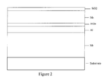
- FIG. 2 shows a modification of the prior art process whereby dielectric layer of SiO 2 is deposited to act as an adhesion layer between the Nb and the photoresist layer deposited during the next process step.
- FIG. 3 shows application of a photoresist layer on top of the silicon dioxide layer in accordance with one aspect of the invention.
- FIG. 4 shows the photoresist area that defines the junction area after exposure and development of the photoresist.
- FIG. 5 shows the etching of the SiO 2 adhesion layer and Nb counter-electrode down to the AlO x /Al barrier layer.
- FIG. 6A shows the results of a selective anodization step whereby all the exposed Al and part of the underlying Nb are converted to insulating oxides.
- FIG. 6B shows a magnified view of the region inside the small dashed box in FIG. 6A .
- FIG. 7 shows the removal of the photoresist layer.
- FIG. 8 shows the result of coating and patterning of another photoresist layer designed to produce a protective anodization ring around the junction area.
- FIG. 9 shows the etching (by Ar ion milling or dry reactive ion etching) of the anodized oxide (both AlO x and NbO x layers) except in the anodization ring (under the photoresist mask)
- FIG. 10 shows the removal of the photoresist defining the anodization ring.
- FIG. 11 shows the deposition of an SiO 2 insulating layer, designed to isolate the junction from subsequent wiring layers.
- FIG. 12 shows the coating and patterning of a third photoresist layer, designed to produce a contact via to the Nb junction from a Nb wiring layer.
- FIG. 13 shows the selective etching of the SiO 2 up to the Nb counter-electrode.
- FIG. 14 shows the removal of the photoresist. Now the structure is ready for deposition of a Nb wiring layer
- a new fabrication method is proposed for increasing the yield and quality of superconducting junctions and more particularly Josephson junctions and Josephson-based digital and analog circuits in superconducting electronics.
- the method is based on using a double-layer mask for partial anodization of the junction side-walls and base-electrode around the junction.
- the top layer of this mask is a photoresist or electron-beam resist, and the bottom layer is a dielectric (e.g., SiO 2 ) that is insoluble in either aqueous or organic solvents.
- the existing fabrication scheme for making Nb-based Josephson tunnel junctions for superconducting electronics is comprised of the following fabrication steps:
- a Nb/Al/AlO x /Nb trilayer is deposited in-situ on a wafer that includes or will include several other patterned layers of metal and dielectric.
- a tunnel barrier is formed by in-situ thermal oxidation of the Al layer in oxygen or an oxygen/argon mixture at a defined pressure, to form a thin ( ⁇ 1-2 nm) layer of AlO x . Both the oxidation time and the pressure determine the properties of the tunnel barrier such as the Josephson critical current density J c .
- the bottom Nb layer is called the base electrode, and the top Nb layer is called the counter-electrode of the tunnel Josephson junctions.
- FIG. 2 shows a step that differs from prior art fabrication techniques and will be discussed in more detail hereinafter.
- the wafer is coated with either positive or negative resist ( FIG. 3 ), and the resist etch mask is formed by optical or e-beam lithography ( FIG. 4 ).
- the counter-electrode area is then defined by etching ( FIG. 5 ), using e.g. plasma etching, reactive-ion etching, or high-density plasma etching.
- the AlO x /Al layer acts as an etch stop. (Note—the prior art method does not include the thin SiO 2 layer shown in FIGS. 3, 4 and 5 .)
- the wafer is immersed in an anodization solution, and all the surfaces that are not protected by the resist mask formed in step 5 are anodized. That is, the same resist etch mask is also used as an anodization mask.
- Anodization creates a bilayer of anodized Al (AlO x ) and anodized Nb (NbO x ) on the surface of the base electrode ( FIG. 6 ). A layer of anodized Nb is also formed on all sidewalls of the junction's counter-electrode.
- This anodization step is very important because it encapsulates the junction's tunnel barrier with an anodized NbO x layer, and this, protects it from reacting with water, oxygen, and other processing chemicals during all further wafer processing steps. This step also allows for opening a contact hole to the counter-electrode that is larger in size than the junction itself.
- the thickness of the anodized layer is controlled by the anodization voltage, usually in the range of 15-50 V.
- the initial anodization current density is in the range from 0.5-5 mA/cm 2 .
- the resist is stripped ( FIG. 7 ), and the wafer proceeds to the next fabrication steps that are intended to pattern the base electrode of the junction by lithography and etching. This may also require removing the anodization layer in some parts of the circuit. It remains around the junction (the anodization ring of FIGS. 8-10 ).
- the Josephson junction is completely formed. All other fabrication steps are necessary in order to interconnect junctions in the circuits (such as the SiO 2 insulating layer in FIGS. 11-14 ), and to create resistors for biasing and shunting the junctions. These steps may vary depending on the details the fabrication process.
- One improvement of the invention is to use a double-layer anodization mask with the lower layer being an inorganic dielectric layer (such as SiO 2 ) that is insoluble in water, solvents, and components of the anodization solution, and the upper layer is the photoresist (or e-beam resist) layer.
- SiO 2 is especially suitable since it has already been optimized as an insulating layer in the prior-art Nb integrated circuit process, and is also fully compatible with standard Si-based resist processing.
- This double-layer mask is formed in the following simple way:
- a pinhole-free layer of SiO 2 is deposited by any appropriate method (e.g., rf magnetron sputtering, or plasma-enhanced chemical vapor deposition—PECVD) on top of the trilayer (see FIG. 2 ).
- the layer thickness may be anywhere from 5 to 300 nm, and is not critical, as long as it is free from pinholes. Thicker layers require long etch times, making them impractical.
- a resist mask is formed in the same way as in step 4 above.
- etching is done, using reactive ion etching (RIE) or inductively coupled plasma (ICP) with fluorine-based chemistry (e.g., SF 6 , NF 3 , or CF 4 +O 2 ) such that both the SiO 2 overlayer and the Nb counter-electrode are etched in the same process.
- RIE reactive ion etching
- ICP inductively coupled plasma
- fluorine-based chemistry e.g., SF 6 , NF 3 , or CF 4 +O 2
- fluorine-based chemistry e.g., SF 6 , NF 3 , or CF 4 +O 2
- the advantages of the proposed method are as follows.
- the SiO 2 layer improves the adhesion of the resist, and does not allow the anodization solution to leach underneath. Since the adhesion of sputtered or PECVD-deposited SiO 2 to Nb has already been optimized, and is stronger than the adhesion of the resist to Nb, the double-layer also protects the junction counter-electrode from being anodized even in the unlikely event that a part of the resist mask pops off, or if the anodization solution does leach under the resist. In the rare case that the SiO 2 layer has a pinhole or other defect, the presence of the resist on top still provides protection during the anodization. The probability that both layers of the double-layer anodization mask fail in the same location is much smaller than the probability of a failure of a single-layer resist mask. As a result, a dramatic increase in the yield and junction quality is achieved.
- FIGS. 8 and 9 Another improvement over the prior art is described in reference to FIGS. 8 and 9 , in defining the anodization ring around the Josephson junction.
- the AlO x layer was first removed by a wet etch process, followed by reactive ion etching (RIE) for removing the NbO x layer.
- RIE reactive ion etching
- a wet etch process can cause problems, that should preferably be avoided in high-reliability VLSI processing, particularly if sub-micron resolution is required.
- this wet etch step is discarded, and two new approaches have been successfully demonstrated.
- approach A ion-milling with a neutral beam of argon (Ar) atoms is used to remove both the AlO x and the NbO x layers.
- Approach B plasma etching (RIE or ICP) is used in a two-step process. First, a chlorine-based plasma is used to remove AlO x , and then a fluorine-based plasma is used to remove the NbO x . Either approach provides for increased yield and uniformity.
- RIE plasma etching
Abstract
An improved microfabrication technique for Josephson junctions in superconducting integrated circuits, based on the use of a double-layer lithographic mask for partial anodization of the side-walls and base electrode of the junctions. The top layer of the mask is a resist material, and the bottom layer is a dielectric material chosen so to maximize adhesion between the resist and the underlying superconducting layer, be etch-compatible with the underlying superconducting layer, and be insoluble in the resist and anodization processing chemistries. The superconductor is preferably niobium, under a silicon dioxide layer, with a conventional photoresist or electron-beam resist as the top layer. This combination results in a substantial increase in the fabrication yield of high-density superconducting integrated circuits, increase in junction uniformity and reduction in defect density. A dry etch more compatible with microlithography may be employed.
Description
This application is a Division of Ser. No. 13/771,330, filed Feb. 20, 2013, now U.S. Pat. No. 9,136,457, issued Sep. 15, 2015, which is a Continuation of Ser. No. 13/073,954, filed Mar. 28, 2011, issued Feb. 26, 2013 as U.S. Pat. No. 8,383,426, which is a Continuation of Ser. No. 12/346,603, filed Dec. 30, 2008, which is a Continuation of Ser. No. 11/616,382, filed Dec. 27, 2006, now U.S. Pat. No. 7,615,385, which are each expressly incorporated herein by reference. This application is related to and claims priority to Provisional Application 60/826,262 filed Sep. 20, 2006 by inventor Sergey K. Tolpygo entitled A Double-Masking Technique for Increasing Fabrication Yield and Josephson Junction Quality in Superconducting Electronics, the contents of which is incorporated herein by reference in its entirety.
This invention was developed in part under contract number N0014-03-C-0370 from the Office of Naval Research. The government has certain rights in this invention.
1. Field of the Invention
The invention is directed to fabrication of electronic devices and more particularly to the fabrication of superconducting electronic devices such as Josephson junctions.
2. Description of the Prior Art
Superconducting integrated circuits (ICs) based on Josephson junctions offer the possibility of operation at clock frequencies of 100 GHz or above. In order to achieve this on an industrial scale, it is necessary to decrease junction size toward submicron dimensions, and increase junction density, so that chips with many thousands of Josephson junctions can be reliably manufactured. The key parameter is the critical current Ic of a junction, which must be defined to within about 1% of design specifications, without defects.
The most reliable junction fabrication technology is based on the superconductor niobium (Nb), and in particular on a trilayer structure based on an ultrathin insulating “tunnel barrier” layer of aluminum oxide (AlOx), 1-2 nm thick, sandwiched between two layers of Nb. This provides a precise critical current density of the junction Jc=Ic/A, where A is the junction area. If the microlithography defines A accurately, without damaging the tunnel barrier layer, then Ic is also accurately defined. This becomes increasingly difficult as the dimensions of the junction decrease. Applications of standard microlithography techniques may produce junctions with edge damage that can reduce junction quality and yield.
Current Nb IC technology also incorporates multiple layers of superconducting Nb wiring to bias and connect the Josephson junctions. This requires high-quality insulating layers between Nb layers, which are typically provided by silicon dioxide (SiO2). SiO2 is of course a standard material in semiconductor technology, and standard procedures for fabricating high-quality films are available.
An established technique in the prior art to improve junction yield is the use of selective anodization (Meng 2003, Kerber 2006). Anodization is an electrolytic process of surface oxidation that passivates all exposed Nb and Al surfaces, preventing damage in subsequent lithographic steps. However, this has not completely eliminated defects and related yield problems. It is essential to solve these problems to advance to the next stage of circuit integration.
As indicated above, the techniques of the prior art have resulted in a number of problems. Specifically, the techniques of the prior art have resulted in low yield, that is, a large number of junctions fabricated on a silicon based wafer fail for a variety of reasons. This results in a substantial percentage of defective junctions on each wafer.
Sometimes part of a junction will simply peel off the wafer upon which it is fabricated, due in part to local stresses that result from the anodization procedure. Further, the prior art does not allow precise control of critical current densities of a junction. Yet another problem stems from the fact that the standard process includes a wet-etching step to remove the anodized AlOx layer, which also limits device yield.
Maintaining ideal adhesion between layers is essential for microlithographic control, and is especially critical during the selective anodization step of junction definition. During this step, penetration of the anodization solution (the electrolyte) under the resist would cause major fabrication defects. Standard resists have been optimized for the semiconductor industry, where the most critical materials are Si and SiO2, and adhesion of resists to these materials is outstanding. In contrast, no such optimization exists for Nb, the key material for superconducting circuits. In the present invention (see FIG. 2 ), a thin layer of SiO2 is used as an adhesion layer in a double-layer mask for defining the area of Josephson junctions. The SiO2 adheres well to Nb (since it has also been optimized for an insulation layer), and also adheres very well to the top resist layer. Furthermore, SiO2 is inert with respect to both aqueous and organic solvents used in anodization processing and resist processing (for both positive and negative resists), but can also be removed where necessary by standard etching techniques.
The invention recognizes that failure of interlayer adhesion between photoresist and Nb is a major cause of defects in the fabrication technology of the prior art. By substantially improving such adhesion, the present invention offers the possibility of improved reliability and IC yield.
In the prior art, the very same photoresist mask had to survive two subsequent fabrication steps—etching and self-aligned junction anodization (passivation) without loss of adhesion. The new technique is more robust in this respect since the bottom layer of the double-layer would prevent defect formation during anodization even if the top (resist) layer fails. This technique has been incorporated into a complete IC process, and indeed has resulted in substantially improved IC yield, especially for the smallest junctions (below 1.5 microns size) where the problems had previously been the most severe.
The present invention does increase the number of steps in the full process, since the SiO2 layer in the mask must first be deposited, and subsequently etched away. (However, this etch-away step can be done simultaneously with the counter-electrode etching.) Nevertheless, this extra effort is easily worthwhile, since it enables the manufacturing (with reasonable yield) of higher-density superconducting ICs with greatly enhanced device speed and performance.
A second process improvement of the present invention replaces a wet-etch process for AlOx removal in the prior art with an optimized dry-etch (or argon ion mill) process, in order to enhance junction uniformity and yield for small junctions.
A detailed description of a preferred embodiment of the invention, including a step-by-step process with fabrication parameters, is shown below.
A new fabrication method is proposed for increasing the yield and quality of superconducting junctions and more particularly Josephson junctions and Josephson-based digital and analog circuits in superconducting electronics. The method is based on using a double-layer mask for partial anodization of the junction side-walls and base-electrode around the junction. The top layer of this mask is a photoresist or electron-beam resist, and the bottom layer is a dielectric (e.g., SiO2) that is insoluble in either aqueous or organic solvents. A more detailed description will now be given.
The existing fabrication scheme for making Nb-based Josephson tunnel junctions for superconducting electronics is comprised of the following fabrication steps:
1. As shown in FIG. 1 , a Nb/Al/AlOx/Nb trilayer is deposited in-situ on a wafer that includes or will include several other patterned layers of metal and dielectric. A tunnel barrier is formed by in-situ thermal oxidation of the Al layer in oxygen or an oxygen/argon mixture at a defined pressure, to form a thin (˜1-2 nm) layer of AlOx. Both the oxidation time and the pressure determine the properties of the tunnel barrier such as the Josephson critical current density Jc. The bottom Nb layer is called the base electrode, and the top Nb layer is called the counter-electrode of the tunnel Josephson junctions.
2. FIG. 2 shows a step that differs from prior art fabrication techniques and will be discussed in more detail hereinafter.
3. The wafer is coated with either positive or negative resist (FIG. 3 ), and the resist etch mask is formed by optical or e-beam lithography (FIG. 4 ). The counter-electrode area is then defined by etching (FIG. 5 ), using e.g. plasma etching, reactive-ion etching, or high-density plasma etching. The AlOx/Al layer acts as an etch stop. (Note—the prior art method does not include the thin SiO2 layer shown in FIGS. 3, 4 and 5 .)
4. After etching and without removing the resist, the wafer is immersed in an anodization solution, and all the surfaces that are not protected by the resist mask formed in step 5 are anodized. That is, the same resist etch mask is also used as an anodization mask. Anodization creates a bilayer of anodized Al (AlOx) and anodized Nb (NbOx) on the surface of the base electrode (FIG. 6 ). A layer of anodized Nb is also formed on all sidewalls of the junction's counter-electrode. This anodization step is very important because it encapsulates the junction's tunnel barrier with an anodized NbOx layer, and this, protects it from reacting with water, oxygen, and other processing chemicals during all further wafer processing steps. This step also allows for opening a contact hole to the counter-electrode that is larger in size than the junction itself. The thickness of the anodized layer is controlled by the anodization voltage, usually in the range of 15-50 V. The initial anodization current density is in the range from 0.5-5 mA/cm2.
5. After anodization, the resist is stripped (FIG. 7 ), and the wafer proceeds to the next fabrication steps that are intended to pattern the base electrode of the junction by lithography and etching. This may also require removing the anodization layer in some parts of the circuit. It remains around the junction (the anodization ring of FIGS. 8-10 ).
6. After base electrode patterning, the Josephson junction is completely formed. All other fabrication steps are necessary in order to interconnect junctions in the circuits (such as the SiO2 insulating layer in FIGS. 11-14 ), and to create resistors for biasing and shunting the junctions. These steps may vary depending on the details the fabrication process.
One of the main sources of defects and loss of yield in this fabrication scheme is poor adhesion of the resist mask in step 3. Although this fact has not been recognized in the prior art. This may be due in part to the volume expansion of Nb and Al layers during anodization, which places significant local stresses on the photoresist mask. As a result, some parts of the resist mask may peel off during anodization, or anodization solutions may leach under the resist mask. This is especially a problem with many negative resists such as UVN®-30 (Shipley Company, Marlborough Mass.). Some photoresists may also be incompatible with (partially soluble in) the common anodization solutions. In these cases, some junctions may be degraded, or the counter-electrode of some junctions may be partially anodized, thus preventing a good (superconducting) electrical contact to be made to the junctions during the following fabrication steps.
One improvement of the invention is to use a double-layer anodization mask with the lower layer being an inorganic dielectric layer (such as SiO2) that is insoluble in water, solvents, and components of the anodization solution, and the upper layer is the photoresist (or e-beam resist) layer. SiO2 is especially suitable since it has already been optimized as an insulating layer in the prior-art Nb integrated circuit process, and is also fully compatible with standard Si-based resist processing. This double-layer mask is formed in the following simple way:
a. After the Josephson junction trilayer (Nb/Al/AlOx/Nb) is formed as in step 1 above, a pinhole-free layer of SiO2 is deposited by any appropriate method (e.g., rf magnetron sputtering, or plasma-enhanced chemical vapor deposition—PECVD) on top of the trilayer (see FIG. 2 ). The layer thickness may be anywhere from 5 to 300 nm, and is not critical, as long as it is free from pinholes. Thicker layers require long etch times, making them impractical.
b. A resist mask is formed in the same way as in step 4 above.
c. Then etching is done, using reactive ion etching (RIE) or inductively coupled plasma (ICP) with fluorine-based chemistry (e.g., SF6, NF3, or CF4+O2) such that both the SiO2 overlayer and the Nb counter-electrode are etched in the same process. This may be a one-step process when the same etch parameters are used for both layers, or a two-step process when different etch recipes are used for etching first the SiO2 and then the Nb counter-electrode. After completing the etch down to the AlOx/Al layer in the trilayer structure (FIG. 5 ), the top of the Josephson junction will have a double-layer structure (SiO2+resist) that serves as the double-layer anodization mask.
d. Etching is immediately followed by the anodization step 3, without removing the resist mask (FIG. 6 ). Now there is a layer of SiO2 under the resist mask for extra protection.
The advantages of the proposed method are as follows. The SiO2 layer improves the adhesion of the resist, and does not allow the anodization solution to leach underneath. Since the adhesion of sputtered or PECVD-deposited SiO2 to Nb has already been optimized, and is stronger than the adhesion of the resist to Nb, the double-layer also protects the junction counter-electrode from being anodized even in the unlikely event that a part of the resist mask pops off, or if the anodization solution does leach under the resist. In the rare case that the SiO2 layer has a pinhole or other defect, the presence of the resist on top still provides protection during the anodization. The probability that both layers of the double-layer anodization mask fail in the same location is much smaller than the probability of a failure of a single-layer resist mask. As a result, a dramatic increase in the yield and junction quality is achieved.
Another improvement over the prior art is described in reference to FIGS. 8 and 9 , in defining the anodization ring around the Josephson junction. In the prior art, the AlOx layer was first removed by a wet etch process, followed by reactive ion etching (RIE) for removing the NbOx layer. However, a wet etch process can cause problems, that should preferably be avoided in high-reliability VLSI processing, particularly if sub-micron resolution is required. In the process of the present invention, this wet etch step is discarded, and two new approaches have been successfully demonstrated. In approach A, ion-milling with a neutral beam of argon (Ar) atoms is used to remove both the AlOx and the NbOx layers. In approach B, plasma etching (RIE or ICP) is used in a two-step process. First, a chlorine-based plasma is used to remove AlOx, and then a fluorine-based plasma is used to remove the NbOx. Either approach provides for increased yield and uniformity.
While various embodiments of the present invention have been illustrated herein in detail, it should be apparent that modifications and adaptations to those embodiments may occur to those skilled in the art without departing from the scope of the present invention as set forth in the following claims.
Claims (20)
1. A method of forming a superconducting integrated circuit, comprising:
forming an adhesion layer formed directly on top of an upper superconductor layer of a Josephson junction trilayer comprising the upper superconductor, an insulating layer, and a lower superconductor;
forming and patterning a resist layer directly on top of the adhesion layer, to expose portions of the adhesion layer through the resist layer and form resist layer edges;
exposing portions of the insulating layer corresponding to patterning of the resist layer by etching through the exposed portions of the adhesion layer and through the upper superconductor layer;
anodizing portions of the lower superconducting layer underlying the exposed portions of the insulating layer in an anodization solution, to selectively form circuit patterns comprising Josephson junction circuit elements under unexposed portions of the adhesion layer, the anodized portions of the lower superconductor layer being volumetrically expanded with respect to the non-anodized portions of the lower superconductor layer to form a layer of anodized superconductor on exposed sidewalls of the upper superconductor and insulating layer, inducing stresses on the adjacent resist layer edges; and
preventing peeling of the resist layer and leeching of etching solution under the resist layer subject to the anodization-induced stresses on the adjacent resist layer edges, by adhesion of the adhesion layer to the resist layer,
wherein in an absence of the adhesion layer with direct deposition of the resist layer on the upper superconductor layer, the resist layer would peel from the upper superconductor layer and the anodization solution would leech under the resist layer, causing fabrication defects, and
wherein the adhesion layer is a thin layer subject to pinhole defects, and wherein the resist layer covers the pinhole defects of the adhesion layer during the anodizing.
2. The method according to claim 1 , wherein the adhesion layer comprises silicon dioxide.
3. The method according to claim 1 , wherein the lower superconductor layer comprises niobium.
4. The method according to claim 1 , wherein the insulating layer comprises aluminum oxide formed by oxidizing a layer of aluminum formed on the lower superconductor layer prior to deposition of the upper superconductor layer, wherein a portion of the lower superconductor layer is anodized through the aluminum oxide.
5. The method according to claim 1 , wherein the Josephson junction trilayer comprises a lower layer of niobium, an insulating layer comprising aluminum oxide, and an upper layer of niobium.
6. The method according to claim 1 , wherein the adhesion layer comprises sputtered or plasma enhanced chemical vapor deposition-deposited SiO2.
7. The method according to claim 1 , wherein the resist comprises UVN®-30 negative photoresist.
8. The method according to claim 1 , wherein the adhesion layer is formed by chemical vapor deposition with a layer thickness of between about 5-300 nm.
9. The method according to claim 1 , wherein the adhesion layer is formed by a sputtering process with a layer thickness of between about 5-300 nm.
10. The method according to claim 1 , wherein the patterns comprising Josephson junction circuit elements circuit comprise at least two separately operating Josephson junctions.
11. A method of forming an integrated circuit having Josephson junctions, comprising:
forming a Josephson junction trilayer comprising an upper superconductor, an insulating layer, and a lower superconductor on a substrate;
depositing an adhesion layer directly on top of the upper superconductor;
forming a resist layer directly on top of the adhesion layer;
patterning and developing the resist layer, to expose portions of the adhesion layer through the resist layer;
etching the exposed portions of the adhesion layer through the upper superconductor to expose the insulating layer;
selectively anodizing portions of the lower superconductor under the exposed portions of the insulating layer, to selectively form Josephson junction circuit elements under remaining portions of the adhesion layer and the resist layer, wherein the anodized portions of the lower superconductor increase in volume with respect to the non-anodized portions under remaining portions of the resist layer and grow beyond the insulating layer to form a layer of anodized lower superconductor on an exposed sidewall of the upper superconductor, the increase in volume inducing stresses on the resist layer at a patterned edge of the resist layer, the adhesion layer having sufficient adhesion to the resist layer and to the upper superconductor to maintain adhesion when subject to the stresses; and
removing at least a portion of the exposed portions of the insulating layer and the anodized portions of the lower superconductor to expose the lower superconductor,
wherein the adhesion layer is a thin layer subject to pinhole defects, and wherein the resist layer covers the pinhole defects during the anodizing.
12. The method according to claim 11 , wherein the Josephson junction trilayer is formed on a silicon substrate and the adhesion layer comprises silicon dioxide.
13. The method according to claim 11 , wherein the Josephson junction circuit elements comprise at least two separately operating Josephson junctions having submicron feature sizes.
14. The method according to claim 11 , wherein the lower superconductor comprises niobium, the insulating layer comprises aluminum oxide, and the upper superconductor comprises niobium.
15. The method according to claim 1 , wherein the resist layer comprises UVN®-30 negative photoresist.
16. The method according to claim 1 , wherein the adhesion layer comprises a dielectric, and the resist comprises at least one of an electron beam exposed resist and a photoresist.
17. The method according to claim 1 , wherein the adhesion layer is formed by chemical vapor deposition or sputtering of SiO2 with a layer thickness of between about 5-300 nm.
18. A method for fabrication of an integrated circuit having Josephson junctions, comprising the steps of:
providing a substrate, having a Josephson junction trilayer thereon comprising a lower superconducting layer, an insulating layer, and an upper superconducting layer, the upper superconducting layer being directly covered by an intermediate layer comprising a dielectric having a thickness of at least 5 nm, which in turn is directly covered by a resist layer;
selectively patterning portions of the resist layer in dependence on an irradiation pattern, and developing the pattered portions of the resist layer to expose portions of the intermediate layer;
etching the exposed portions of the intermediate layer and underlying portions of the upper superconducting layer, substantially without removing remaining portions of the resist layer, to expose the insulating layer, to thereby form a bilayer anodization mask comprising the resist layer and the intermediate layer; and
anodizing the exposed insulating layer and underlying lower superconducting layer through the bilayer mask cause a volumetric increase in at least the lower superconducting layer, such that anodized superconductor of the lower superconductor layer volumetrically expands above the intermediate layer, and stresses are induced in the resist layer, to selectively form Josephson junction circuit elements comprising intact portions of the Josephson junction trilayer protected by the bilayer mask, wherein the resist layer remains strongly adherent to the intermediate layer, and the intermediate layer remains strongly adherent to the upper superconducting layer, substantially without peeling,
wherein the intermediate layer is a thin layer subject to pinhole defects, and wherein the resist layer covers the pinhole defects during the anodizing.
19. The method according to claim 18 , wherein the intermediate layer comprises silicon dioxide, the resist layer is strongly adherent to silicon dioxide, and at least the upper superconducting layer comprises a niobium based superconductor film, wherein the resist is more strongly adherent to silicon dioxide than to the niobium based superconductor film.
20. The method according to claim 18 , wherein:
the substrate is a silicon substrate;
the intermediate layer comprises silicon dioxide deposited by chemical vapor deposition; and
the Josephson junction circuit elements comprise at least two separately operating Josephson junctions having submicron feature sizes, in which the lower superconductor comprises niobium, the insulating layer comprises aluminum oxide, and the upper superconductor comprises niobium.
Priority Applications (2)
| Application Number | Priority Date | Filing Date | Title |
|---|---|---|---|
| US14/850,634 US9595656B2 (en) | 2006-09-20 | 2015-09-10 | Double-masking technique for increasing fabrication yield in superconducting electronics |
| US15/456,010 US10109673B2 (en) | 2006-09-20 | 2017-03-10 | Double-masking technique for increasing fabrication yield in superconducting electronics |
Applications Claiming Priority (6)
| Application Number | Priority Date | Filing Date | Title |
|---|---|---|---|
| US82626206P | 2006-09-20 | 2006-09-20 | |
| US11/616,382 US7615385B2 (en) | 2006-09-20 | 2006-12-27 | Double-masking technique for increasing fabrication yield in superconducting electronics |
| US12/346,603 US20090315021A1 (en) | 2006-09-20 | 2008-12-30 | Double-masking technique for increasing fabrication yield in superconducting electronics |
| US13/073,954 US8383426B1 (en) | 2006-09-20 | 2011-03-28 | Double-masking technique for increasing fabrication yield in superconducting electronics |
| US13/771,330 US9136457B2 (en) | 2006-09-20 | 2013-02-20 | Double-masking technique for increasing fabrication yield in superconducting electronics |
| US14/850,634 US9595656B2 (en) | 2006-09-20 | 2015-09-10 | Double-masking technique for increasing fabrication yield in superconducting electronics |
Related Parent Applications (1)
| Application Number | Title | Priority Date | Filing Date |
|---|---|---|---|
| US13/771,330 Continuation US9136457B2 (en) | 2006-09-20 | 2013-02-20 | Double-masking technique for increasing fabrication yield in superconducting electronics |
Related Child Applications (1)
| Application Number | Title | Priority Date | Filing Date |
|---|---|---|---|
| US15/456,010 Continuation US10109673B2 (en) | 2006-09-20 | 2017-03-10 | Double-masking technique for increasing fabrication yield in superconducting electronics |
Publications (2)
| Publication Number | Publication Date |
|---|---|
| US20150380632A1 US20150380632A1 (en) | 2015-12-31 |
| US9595656B2 true US9595656B2 (en) | 2017-03-14 |
Family
ID=39189122
Family Applications (6)
| Application Number | Title | Priority Date | Filing Date |
|---|---|---|---|
| US11/616,382 Active 2027-06-15 US7615385B2 (en) | 2006-09-20 | 2006-12-27 | Double-masking technique for increasing fabrication yield in superconducting electronics |
| US12/346,603 Abandoned US20090315021A1 (en) | 2006-09-20 | 2008-12-30 | Double-masking technique for increasing fabrication yield in superconducting electronics |
| US13/073,954 Active US8383426B1 (en) | 2006-09-20 | 2011-03-28 | Double-masking technique for increasing fabrication yield in superconducting electronics |
| US13/771,330 Active 2027-05-14 US9136457B2 (en) | 2006-09-20 | 2013-02-20 | Double-masking technique for increasing fabrication yield in superconducting electronics |
| US14/850,634 Active US9595656B2 (en) | 2006-09-20 | 2015-09-10 | Double-masking technique for increasing fabrication yield in superconducting electronics |
| US15/456,010 Active US10109673B2 (en) | 2006-09-20 | 2017-03-10 | Double-masking technique for increasing fabrication yield in superconducting electronics |
Family Applications Before (4)
| Application Number | Title | Priority Date | Filing Date |
|---|---|---|---|
| US11/616,382 Active 2027-06-15 US7615385B2 (en) | 2006-09-20 | 2006-12-27 | Double-masking technique for increasing fabrication yield in superconducting electronics |
| US12/346,603 Abandoned US20090315021A1 (en) | 2006-09-20 | 2008-12-30 | Double-masking technique for increasing fabrication yield in superconducting electronics |
| US13/073,954 Active US8383426B1 (en) | 2006-09-20 | 2011-03-28 | Double-masking technique for increasing fabrication yield in superconducting electronics |
| US13/771,330 Active 2027-05-14 US9136457B2 (en) | 2006-09-20 | 2013-02-20 | Double-masking technique for increasing fabrication yield in superconducting electronics |
Family Applications After (1)
| Application Number | Title | Priority Date | Filing Date |
|---|---|---|---|
| US15/456,010 Active US10109673B2 (en) | 2006-09-20 | 2017-03-10 | Double-masking technique for increasing fabrication yield in superconducting electronics |
Country Status (1)
| Country | Link |
|---|---|
| US (6) | US7615385B2 (en) |
Cited By (1)
| Publication number | Priority date | Publication date | Assignee | Title |
|---|---|---|---|---|
| US10109673B2 (en) * | 2006-09-20 | 2018-10-23 | Hypres, Inc. | Double-masking technique for increasing fabrication yield in superconducting electronics |
Families Citing this family (23)
| Publication number | Priority date | Publication date | Assignee | Title |
|---|---|---|---|---|
| CA2751897C (en) | 2009-02-27 | 2018-01-09 | D-Wave Systems Inc. | Systems and methods for fabrication of superconducting integrated circuits |
| US8301214B1 (en) | 2010-01-08 | 2012-10-30 | Hypres, Inc. | System and method for providing multi-conductive layer metallic interconnects for superconducting integrated circuits |
| JP6326379B2 (en) | 2012-03-08 | 2018-05-16 | ディー−ウェイブ システムズ,インコーポレイテッド | System and method for fabrication of superconducting integrated circuits |
| US9741918B2 (en) * | 2013-10-07 | 2017-08-22 | Hypres, Inc. | Method for increasing the integration level of superconducting electronics circuits, and a resulting circuit |
| US9324767B1 (en) * | 2013-12-31 | 2016-04-26 | Intermolecular, Inc. | Superconducting junctions |
| US9520180B1 (en) | 2014-03-11 | 2016-12-13 | Hypres, Inc. | System and method for cryogenic hybrid technology computing and memory |
| US10454015B2 (en) | 2014-08-13 | 2019-10-22 | D-Wave Systems Inc. | Method of forming superconducting wiring layers with low magnetic noise |
| US9576894B2 (en) * | 2015-06-03 | 2017-02-21 | GlobalFoundries, Inc. | Integrated circuits including organic interlayer dielectric layers and methods for fabricating the same |
| US10763420B2 (en) | 2016-06-13 | 2020-09-01 | Intel Corporation | Josephson Junction damascene fabrication |
| WO2018030977A1 (en) * | 2016-08-08 | 2018-02-15 | Intel Corporation | Josephson junctions formed by partially subtractive fabrication |
| US9865795B1 (en) * | 2016-09-30 | 2018-01-09 | The United States Of America As Represented By The Administrator Of The National Aeronautics And Space Administration | Process for fabrication of superconducting vias for electrical connection to groundplane in cryogenic detectors |
| EP3563430B1 (en) | 2016-12-30 | 2022-02-02 | Teknologian tutkimuskeskus VTT Oy | Superconductive junction, superconducting apparatus and control method of superconducting junction |
| EP3577700B1 (en) | 2017-02-01 | 2022-03-30 | D-Wave Systems Inc. | Systems and methods for fabrication of superconducting integrated circuits |
| US10367134B2 (en) * | 2017-06-07 | 2019-07-30 | International Business Machines Corporation | Shadow mask sidewall tunnel junction for quantum computing |
| US11385099B1 (en) | 2017-06-26 | 2022-07-12 | SeeQC Inc. | Integrated superconducting nanowire digital photon detector |
| US10243132B1 (en) | 2018-03-23 | 2019-03-26 | International Business Machines Corporation | Vertical josephson junction superconducting device |
| US10672971B2 (en) | 2018-03-23 | 2020-06-02 | International Business Machines Corporation | Vertical transmon qubit device with microstrip waveguides |
| US10256392B1 (en) | 2018-03-23 | 2019-04-09 | International Business Machines Corporation | Vertical transmon qubit device |
| CN108539004B (en) * | 2018-04-25 | 2023-12-05 | 中国科学院上海微系统与信息技术研究所 | Submicron Josephson tunnel junction and preparation method thereof |
| US20200152851A1 (en) | 2018-11-13 | 2020-05-14 | D-Wave Systems Inc. | Systems and methods for fabricating superconducting integrated circuits |
| US11683995B2 (en) | 2020-08-03 | 2023-06-20 | International Business Machines Corporation | Lithography for fabricating Josephson junctions |
| US11737373B2 (en) | 2020-09-30 | 2023-08-22 | International Business Machines Corporation | Silicide passivation of niobium |
| CN112670401B (en) * | 2020-12-21 | 2022-10-14 | 中国科学院上海微系统与信息技术研究所 | Josephson junction and superconducting device and preparation method thereof |
Citations (581)
| Publication number | Priority date | Publication date | Assignee | Title |
|---|---|---|---|---|
| US3936809A (en) | 1974-06-07 | 1976-02-03 | International Business Machines Corporation | Single flux quantum storage devices and sensing means therefor |
| US3943383A (en) | 1974-04-23 | 1976-03-09 | International Business Machines Corporation | Superconductive circuit level converter |
| US3953749A (en) | 1973-12-13 | 1976-04-27 | International Business Machines Corporation | Binary circuitry including switching elements utilizing superconductive tunneling effects |
| US3962628A (en) | 1975-04-14 | 1976-06-08 | The United States Of America As Represented By The Secretary Of The Navy | Adjustable magnetic gradiometer |
| US3970965A (en) | 1975-03-26 | 1976-07-20 | The United States Of America As Represented By The Secretary Of The Navy | Injection locked Josephson oscillator systems |
| US3976938A (en) | 1974-12-09 | 1976-08-24 | Superconducting Technology, Inc. | Superconducting magnetic sensor with improved balancing system |
| US3978351A (en) | 1975-06-30 | 1976-08-31 | International Business Machines Corporation | Quantum interference josephson logic devices |
| US3980076A (en) | 1974-10-02 | 1976-09-14 | The Board Of Trustees Of Leland Stanford Junior University | Method for measuring externally of the human body magnetic susceptibility changes |
| US4008411A (en) | 1975-07-08 | 1977-02-15 | The United States Of America As Represented By The United States Energy Research And Development Administration | Production of 14 MeV neutrons by heavy ions |
| US4009479A (en) | 1973-03-30 | 1977-02-22 | L'air Liquide, Societe Anonyme Pour L'etude Et L'exploitation Des Procedes Georges Claude | Josephson junction |
| US4025844A (en) | 1975-04-24 | 1977-05-24 | Ramot University Authority For Applied Research And Industrial Development Ltd. | Granular superconducting quantum interference device and apparatus including same |
| US4028714A (en) | 1974-12-31 | 1977-06-07 | International Business Machines Corporation | Ultralow-power, micro-miniaturized Josephson devices having high inductance |
| US4039856A (en) | 1975-12-02 | 1977-08-02 | International Business Machines Corporation | Distributed josephson junction logic circuit |
| US4055847A (en) | 1976-08-13 | 1977-10-25 | Nasa | Germanium coated microbridge and method |
| US4075756A (en) | 1976-06-30 | 1978-02-28 | International Business Machines Corporation | Process for fabricating above and below ground plane wiring on one side of a supporting substrate and the resulting circuit configuration |
| US4079730A (en) | 1974-10-02 | 1978-03-21 | The Board Of Trustees Of The Leland Stanford Junior University | Apparatus for measuring externally of the human body magnetic susceptibility changes |
| US4082991A (en) | 1974-07-11 | 1978-04-04 | James Nickolas Constant | Superconducting energy system |
| US4097765A (en) | 1976-06-30 | 1978-06-27 | International Business Machines Corporation | Electronically alterable non-latching Josephson AND, OR, NAND, NOR logic circuit |
| US4107554A (en) | 1976-06-30 | 1978-08-15 | International Business Machines Corporation | Data bus arrangement for Josephson tunneling device logic interconnections |
| US4109522A (en) | 1974-11-22 | 1978-08-29 | Chevron Research Company | Method of borehole logging using passive Josephson current detector to directly determine the presence of hydrocarbons |
| US4117503A (en) | 1977-06-30 | 1978-09-26 | International Business Machines Corporation | Josephson interferometer structure which suppresses resonances |
| US4130893A (en) | 1977-03-29 | 1978-12-19 | International Business Machines Corporation | Josephson memory cells having improved NDRO sensing |
| US4143520A (en) | 1977-12-23 | 1979-03-13 | The United States Of America As Represented By The Secretary Of The Navy | Cryogenic refrigeration system |
| US4163156A (en) | 1976-05-19 | 1979-07-31 | International Business Machines Corporation | Method of modifying the performance characteristics of a Josephson junction |
| US4176365A (en) | 1978-05-08 | 1979-11-27 | Sperry Rand Corporation | Josephson tunnel junction device with hydrogenated amorphous silicon, germanium or silicon-germanium alloy tunneling barrier |
| US4176029A (en) | 1978-03-02 | 1979-11-27 | Sperry Rand Corporation | Subminiature bore and conductor formation |
| US4177476A (en) | 1978-05-05 | 1979-12-04 | Sperry Rand Corporation | Multiple weak-link SQUID with non-superconductive material weak-links |
| US4178602A (en) | 1977-08-31 | 1979-12-11 | Kandyba Petr E | Thin film cryotron |
| US4186441A (en) | 1977-11-14 | 1980-01-29 | International Business Machines Corporation | Magnetic vortex generator with a vortex pool and single vortex transfer |
| US4220959A (en) | 1979-03-23 | 1980-09-02 | Sperry Corporation | Josephson tunnel junction with polycrystalline silicon, germanium or silicon-germanium alloy tunneling barrier |
| US4224630A (en) | 1978-08-25 | 1980-09-23 | Sperry Corporation | Multiple weak-link SQUID |
| US4225818A (en) | 1977-11-10 | 1980-09-30 | National Research Development Corporation | Cryogenic nuclear gyroscope |
| US4227096A (en) | 1978-08-31 | 1980-10-07 | Nasa | Microwave integrated circuit for Josephson voltage standards |
| US4253230A (en) | 1979-02-09 | 1981-03-03 | The United States Of America As Represented By The Secretary Of The Navy | Silicon barrier Josephson junction configuration |
| US4255465A (en) | 1973-08-28 | 1981-03-10 | Commissariat A L'energie Atomique | Method of producing Josephson-effect junctions |
| US4263603A (en) | 1978-03-02 | 1981-04-21 | Sperry Corporation | Subminiature bore and conductor formation |
| US4266008A (en) | 1979-11-23 | 1981-05-05 | The United States Of America As Represented By The United States Department Of Energy | Method for etching thin films of niobium and niobium-containing compounds for preparing superconductive circuits |
| US4280095A (en) | 1979-03-22 | 1981-07-21 | The United States Of America As Represented By The Secretary Of The Navy | Extremely sensitive super conducting quantum interference device constructed as a double-helix array |
| US4295147A (en) | 1980-02-01 | 1981-10-13 | International Business Machines Corp. | Josephson devices of improved thermal cyclability and method |
| US4299679A (en) | 1978-12-27 | 1981-11-10 | Fujitsu Limited | Method of producing Josephson elements of the tunneling junction type |
| US4313066A (en) | 1979-08-20 | 1982-01-26 | International Business Machines Corporation | Direct coupled nonlinear injection Josephson logic circuits |
| US4316200A (en) | 1980-03-07 | 1982-02-16 | International Business Machines Corporation | Contact technique for electrical circuitry |
| US4320341A (en) | 1980-01-17 | 1982-03-16 | Sperry Corporation | Method and apparatus for balancing the magnetic field detecting loops of a cryogenic gradiometer using trimming coils and superconducting disks |
| US4326188A (en) | 1979-07-03 | 1982-04-20 | Licentia Patent-Verwaltungs-G.M.B.H. | Magnetically controllable variable resistor |
| US4333808A (en) | 1979-10-30 | 1982-06-08 | International Business Machines Corporation | Method for manufacture of ultra-thin film capacitor |
| US4339508A (en) | 1977-11-28 | 1982-07-13 | Shiro Maeda | Method for manufacturing a thin and flexible ribbon of superconductor material |
| US4344052A (en) | 1980-09-29 | 1982-08-10 | International Business Machines Corporation | Distributed array of Josephson devices with coherence |
| US4351712A (en) | 1980-12-10 | 1982-09-28 | International Business Machines Corporation | Low energy ion beam oxidation process |
| US4364167A (en) | 1979-11-28 | 1982-12-21 | General Motors Corporation | Programming an IGFET read-only-memory |
| US4366494A (en) | 1980-05-20 | 1982-12-28 | Rikagaku Kenkyusho | Josephson junction and a method of making the same |
| US4368479A (en) | 1979-02-09 | 1983-01-11 | The United States Of America As Represented By The Secretary Of The Navy | Silicon barrier Josephson junction configuration |
| US4370359A (en) | 1980-08-18 | 1983-01-25 | Bell Telephone Laboratories, Incorporated | Fabrication technique for junction devices |
| US4386361A (en) | 1980-09-26 | 1983-05-31 | S.H.E. Corporation | Thin film SQUID with low inductance |
| US4392148A (en) | 1980-12-31 | 1983-07-05 | International Business Machines Corporation | Moat-guarded Josephson devices |
| US4395813A (en) | 1980-10-22 | 1983-08-02 | Hughes Aircraft Company | Process for forming improved superconductor/semiconductor junction structures |
| US4403189A (en) | 1980-08-25 | 1983-09-06 | S.H.E. Corporation | Superconducting quantum interference device having thin film Josephson junctions |
| US4409262A (en) | 1982-02-01 | 1983-10-11 | The United States Of America As Represented By The Secretary Of The Navy | Fabrication of submicron-wide lines with shadow depositions |
| US4412902A (en) | 1981-06-22 | 1983-11-01 | Nippon Telegraph & Telephone Public Corporation | Method of fabrication of Josephson tunnel junction |
| US4414738A (en) | 1981-02-02 | 1983-11-15 | The United States Of America As Represented By The Secretary Of The Navy | Optical lithographic technique for fabricating submicron-sized Josephson microbridges |
| US4418095A (en) | 1982-03-26 | 1983-11-29 | Sperry Corporation | Method of making planarized Josephson junction devices |
| US4421785A (en) | 1980-08-18 | 1983-12-20 | Sperry Corporation | Superconductive tunnel junction device and method of manufacture |
| US4423430A (en) | 1980-02-20 | 1983-12-27 | Fujitsu Limited | Superconductive logic device |
| US4426268A (en) | 1983-07-12 | 1984-01-17 | The United States Of America As Represented By The Secretary Of The Navy | Method for forming high superconducting Tc niobium nitride film at ambient temperatures |
| US4430662A (en) | 1981-04-09 | 1984-02-07 | Sperry Corporation | Superconductive tunnel junction integrated circuit |
| US4430790A (en) | 1980-05-20 | 1984-02-14 | Rikagaku Kenkyusho | Method of making a Josephson junction |
| US4432134A (en) | 1982-05-10 | 1984-02-21 | Rockwell International Corporation | Process for in-situ formation of niobium-insulator-niobium Josephson tunnel junction devices |
| US4434547A (en) | 1980-05-05 | 1984-03-06 | Commissariat A L'energie Atomique | Process for the manufacture and adjustment of a Josephson effect magnetic flux pick-up |
| US4437227A (en) | 1982-10-28 | 1984-03-20 | Sperry Corporation | Method of making improved tunnel barriers for superconducting Josephson junction devices |
| US4439269A (en) | 1982-09-30 | 1984-03-27 | The United States Of America As Represented By The Secretary Of The Navy | Method for making Josephson junctions with contamination-free interfaces utilizing a ZnO contact insulator |
| US4454522A (en) | 1981-11-05 | 1984-06-12 | The Board Of Trustees Of The Leland Stanford Junior University | Microbridge superconducting device having support with stepped parallel surfaces |
| US4456506A (en) | 1982-01-28 | 1984-06-26 | Sperry Corporation | Superconducting circuit fabrication |
| US4459321A (en) | 1982-12-30 | 1984-07-10 | International Business Machines Corporation | Process for applying closely overlapped mutually protective barrier films |
| US4458409A (en) | 1982-03-12 | 1984-07-10 | International Business Machines Corporation | Process for producing niobium Josephson junctions |
| US4470190A (en) | 1982-11-29 | 1984-09-11 | At&T Bell Laboratories | Josephson device fabrication method |
| US4474828A (en) | 1983-03-30 | 1984-10-02 | Sperry Corporation | Method of controlling the supercurrent of a Josephson junction device |
| US4490733A (en) | 1982-10-15 | 1984-12-25 | Sperry Corporation | Josephson device with tunneling barrier having low density of localized states and enhanced figures of merit |
| US4490901A (en) | 1983-05-05 | 1985-01-01 | International Business Machines Corporation | Adjustment of Josephson junctions by ion implantation |
| US4495510A (en) | 1980-10-22 | 1985-01-22 | Hughes Aircraft Company | Improved superconductor/semiconductor junction structures |
| US4499119A (en) | 1983-07-06 | 1985-02-12 | Sperry Corporation | Method of manufacturing super-conductive tunnel junction devices with precise junction area control |
| US4514254A (en) | 1983-09-26 | 1985-04-30 | International Business Machines Corporation | Groundplane post-etch anodization |
| US4517253A (en) | 1984-01-23 | 1985-05-14 | Rose Robert M | Cryoelectrodeposition |
| US4517121A (en) | 1981-07-22 | 1985-05-14 | Centre National De La Recherche Scientifique | Method of increasing the supraconductive critical temperature in quasi unidimensional organic supraconductors and new supraconductive compounds thus obtained |
| US4526629A (en) | 1984-05-15 | 1985-07-02 | International Business Machines Corporation | Catalytic oxidation of solid materials |
| US4536414A (en) | 1983-01-17 | 1985-08-20 | Sperry Corporation | Superconductive tunnel junction device with enhanced characteristics and method of manufacture |
| US4536781A (en) | 1983-02-22 | 1985-08-20 | Sperry Corporation | Fabrication of superconductive tunneling junction resistors and short circuits by ion implantation |
| US4536780A (en) | 1983-02-22 | 1985-08-20 | Sperry Corporation | Superconductive tunneling junction resistor and method of fabrication |
| US4544937A (en) | 1983-04-01 | 1985-10-01 | Sperry Corporation | Formation of normal resistors by degenerate doping of substrates |
| US4548834A (en) | 1982-05-31 | 1985-10-22 | Nec Corporation | Method of producing a Josephson tunnel barrier |
| US4554567A (en) | 1983-03-21 | 1985-11-19 | Sperry Corporation | Superconductive integrated circuit incorporating a magnetically controlled interferometer |
| US4560435A (en) | 1984-10-01 | 1985-12-24 | International Business Machines Corporation | Composite back-etch/lift-off stencil for proximity effect minimization |
| US4567438A (en) | 1983-04-04 | 1986-01-28 | Sperry Corporation | SQUID Canister with conical coupling cavity |
| US4585999A (en) | 1984-04-27 | 1986-04-29 | The United States Of America As Represented By The United States Department Of Energy | Radiofrequency amplifier based on a dc superconducting quantum interference device |
| US4589001A (en) | 1980-07-09 | 1986-05-13 | Agency Of Industrial Science & Technology | Quasiparticle injection control type superconducting device |
| US4588947A (en) | 1983-12-30 | 1986-05-13 | International Business Machines Corporation | Integrated miniature DC SQUID susceptometer for measuring properties of very small samples |
| US4589961A (en) | 1984-08-31 | 1986-05-20 | Sperry Corporation | Aluminum mask anodization with lift-off for patterning Josephson junction devices |
| US4623804A (en) | 1983-02-04 | 1986-11-18 | Rikagaku Kenkyusho | Fluxoid type superconducting logic element |
| US4629536A (en) | 1985-03-12 | 1986-12-16 | Energy Conversion Devices, Inc. | Multilayer depth profile method |
| US4647954A (en) | 1983-12-28 | 1987-03-03 | International Business Machines Corporation | Low temperature tunneling transistor |
| US4660061A (en) | 1983-12-19 | 1987-04-21 | Sperry Corporation | Intermediate normal metal layers in superconducting circuitry |
| US4687987A (en) | 1984-09-28 | 1987-08-18 | The United States Of America As Represented By The United States Department Of Energy | Beam current sensor |
| US4689559A (en) | 1984-11-13 | 1987-08-25 | Sperry Corporation | Apparatus and method to reduce the thermal response of SQUID sensors |
| US4693000A (en) | 1984-11-19 | 1987-09-15 | Siemens Aktiengesellschaft | Method for manufacturing a three-dimensional gradiometer for a device for the single or multi-channel measurement of weak magnetic fields |
| US4694567A (en) | 1984-11-19 | 1987-09-22 | Siemens Aktiengesellschaft | Method for making a superconducting gradiometer having a three-dimensional structure and associated connecting lines for a device for measuring weak magnetic fields |
| US4700135A (en) | 1985-04-26 | 1987-10-13 | Siemens Aktiengesellschaft | Apparatus for measuring weak magnetic fields having several gradiometers with associated SQUID array |
| US4715189A (en) | 1985-11-12 | 1987-12-29 | Hypres, Inc. | Open cycle cooling of electrical circuits |
| US4726890A (en) | 1985-08-12 | 1988-02-23 | The United States Of America As Represented By The Administrator Of The National Aeronautics And Space Administration | Method of producing high Tc superconducting NbN films |
| US4733180A (en) | 1985-04-26 | 1988-03-22 | Siemens Aktiengesellschaft | Apparatus for measuring weak magnetic fields having superconducting connections between a squid array and a gradiometer array |
| US4739633A (en) | 1985-11-12 | 1988-04-26 | Hypres, Inc. | Room temperature to cryogenic electrical interface |
| US4749946A (en) | 1982-12-22 | 1988-06-07 | Siemens Aktiengesellschaft | Device for the multi-channel measurement of weak variable magnetic fields with squids and superconducting gradiometers arranged on a common substrate |
| US4749888A (en) | 1984-01-25 | 1988-06-07 | Agency Of Industrial Science & Technology | Josephson transmission line device |
| US4751563A (en) | 1984-11-05 | 1988-06-14 | International Business Machines, Corp. | Microminiaturized electrical interconnection device and its method of fabrication |
| US4761611A (en) | 1985-04-26 | 1988-08-02 | Siemens Aktiengesellschaft | Apparatus for measuring weak magnetic fields having a DC-SQUID array and gradiometer array |
| US4768069A (en) | 1987-03-23 | 1988-08-30 | Westinghouse Electric Corp. | Superconducting Josephson junctions |
| US4777362A (en) | 1986-06-04 | 1988-10-11 | Hypres, Inc. | Particle trigger and delay generation system |
| US4789794A (en) | 1986-09-26 | 1988-12-06 | Hypres Incorporated | Time domain reflectometer |
| US4790903A (en) | 1986-04-28 | 1988-12-13 | University Of Tokyo | Intermittent etching process |
| US4801882A (en) | 1986-05-21 | 1989-01-31 | Siemens Aktiengesellschaft | Thin film SQUID magnetometer for a device for measuring weak magnetic fields |
| US4812689A (en) | 1987-08-28 | 1989-03-14 | Hypres, Inc. | Incremental time delay generator |
| US4844989A (en) | 1987-03-19 | 1989-07-04 | The University Of Chicago (Arch Development Corp.) | Superconducting structure with layers of niobium nitride and aluminum nitride |
| US4856899A (en) | 1985-12-20 | 1989-08-15 | Yokogawa Electric Corporation | Optical frequency analyzer using a local oscillator heterodyne detection of incident light |
| US4857360A (en) | 1986-03-12 | 1989-08-15 | Kernforschungszentrum Karlsruhe Gmbh | Process for the manufacture of NbN superconducting cavity resonators |
| US4860067A (en) | 1986-06-20 | 1989-08-22 | International Business Machines Corporation | Semiconductor heterostructure adapted for low temperature operation |
| US4859879A (en) | 1988-05-16 | 1989-08-22 | Westinghouse Electric Corp. | Superconducting digital logic amplifier |
| US4866302A (en) | 1986-09-26 | 1989-09-12 | Hypres, Incorporated | Time domain reflectometer |
| US4869598A (en) | 1988-03-11 | 1989-09-26 | Mcdonald Donald G | Temperature-sensitive multiple-layer thin film superconducting device |
| US4884111A (en) | 1984-11-05 | 1989-11-28 | Toshikazu Nishino | Superconducting device |
| US4893353A (en) | 1985-12-20 | 1990-01-09 | Yokogawa Electric Corporation | Optical frequency synthesizer/sweeper |
| US4904619A (en) | 1987-03-24 | 1990-02-27 | Hitachi Ltd. | Method of forming Josephson junction devices |
| US4904341A (en) | 1988-08-22 | 1990-02-27 | Westinghouse Electric Corp. | Selective silicon dioxide etchant for superconductor integrated circuits |
| US4904980A (en) | 1988-08-19 | 1990-02-27 | Westinghouse Electric Corp. | Refractory resistors with etch stop for superconductor integrated circuits |
| US4906930A (en) | 1987-02-27 | 1990-03-06 | Hitachi, Ltd. | Magnetometer using a Josephson device and superconducting phototransistor |
| US4911800A (en) | 1988-04-08 | 1990-03-27 | Massachusetts Institute Of Technology | Electrochemically controlled superconductivity |
| US4918328A (en) | 1988-05-03 | 1990-04-17 | Hypres Incorporated | Apparatus and method for generating a step voltage waveform |
| US4918049A (en) | 1987-11-18 | 1990-04-17 | Massachusetts Institute Of Technology | Microwave/far infrared cavities and waveguides using high temperature superconductors |
| US4920093A (en) | 1987-05-29 | 1990-04-24 | Toray Industries, Inc. | Fabrication of superconducting oxide thin films by sol-gel method |
| US4923850A (en) | 1987-10-20 | 1990-05-08 | Thomson-Csf | Superconducting DC SQUID magnetometer working in liquid nitrogen |
| US4927670A (en) | 1988-06-22 | 1990-05-22 | Georgia Tech Research Corporation | Chemical vapor deposition of mixed metal oxide coatings |
| US4937525A (en) | 1986-08-13 | 1990-06-26 | Siemens Aktiengesellschaft | SQUID-magnetometer for measuring weak magnetic fields with gradiometer loops and Josephson tunnel elements on a common carrier |
| US4962316A (en) | 1989-07-31 | 1990-10-09 | Santa Barbara Research Center | Frequency domain integrating resonant superconducting transmission line detector |
| US4963852A (en) | 1989-03-15 | 1990-10-16 | The United States Of America As Represented By The Secretary Of The Air Force | Superconductor switch |
| US4971944A (en) | 1989-02-21 | 1990-11-20 | Westinghouse Electric Corp. | Method of electroless depositing of gold onto superconducting particles |
| US4974205A (en) | 1988-10-24 | 1990-11-27 | Fujitsu Limited | Josephson memory and read/write circuit |
| US4977402A (en) | 1988-10-24 | 1990-12-11 | Hewlett-Packard Company | Nonhysteretic periodic-threshold SQUID comparator and A/D converter |
| US4983971A (en) | 1989-06-29 | 1991-01-08 | Westinghouse Electric Corp. | Josephson analog to digital converter for low-level signals |
| US5012190A (en) | 1987-10-22 | 1991-04-30 | U.S. Philips Corporation | Apparatus for multi-channel measurement of weak magnetic fields with squids and superconducting gradiometers on individual detachable assemblies, and method of manufacture |
| US5013526A (en) | 1988-11-24 | 1991-05-07 | Hitachi, Ltd. | Superconducting alloys comprising tungsten, molybdenum, silicon and oxygen |
| US5019530A (en) | 1990-04-20 | 1991-05-28 | International Business Machines Corporation | Method of making metal-insulator-metal junction structures with adjustable barrier heights |
| US5019721A (en) | 1989-08-18 | 1991-05-28 | Wisconsin Alumni Research Foundation | Active superconducting devices formed of thin films |
| US5019551A (en) | 1987-09-10 | 1991-05-28 | Nec Corporation | Superconducting contact structure |
| US5021658A (en) | 1989-06-29 | 1991-06-04 | Westinghouse Electric Corp. | Superconducting infrared detector |
| US5021867A (en) | 1989-05-30 | 1991-06-04 | Westinghouse Electric Corp. | Refractory resistors with etch stop for superconductor integrated circuits |
| US5024993A (en) | 1990-05-02 | 1991-06-18 | Microelectronics & Computer Technology Corporation | Superconducting-semiconducting circuits, devices and systems |
| US5036042A (en) | 1988-12-29 | 1991-07-30 | International Superconductor Corp. | Switchable superconducting mirrors |
| US5041880A (en) | 1988-06-16 | 1991-08-20 | Sharp Kabushiki Kaisha | Logic device and memory device using ceramic superconducting element |
| US5047390A (en) | 1988-10-03 | 1991-09-10 | Matsushita Electric Industrial Co., Ltd. | Josephson devices and process for manufacturing the same |
| US5049818A (en) | 1989-03-04 | 1991-09-17 | U.S. Philips Corporation | Gradiometer for detecting weak magnetic fields including grooves carrying superconducting thin film conductors and method of making same |
| US5053834A (en) | 1990-08-31 | 1991-10-01 | Quantum Magnetics, Inc. | High symmetry dc SQUID system |
| US5055158A (en) | 1990-09-25 | 1991-10-08 | International Business Machines Corporation | Planarization of Josephson integrated circuit |
| US5055319A (en) | 1990-04-02 | 1991-10-08 | The Regents Of The University Of California | Controlled high rate deposition of metal oxide films |
| US5058431A (en) | 1990-05-23 | 1991-10-22 | The United States Of America As Represented By The Secretary Of The Navy | Superconducting Josephson junction gyroscope apparatus |
| US5065096A (en) | 1989-09-21 | 1991-11-12 | Forschungszentrum Julich Gmbh | Superconductor Josephson junction strip resonator sensor for measuring magnetic flux |
| US5064809A (en) | 1988-12-23 | 1991-11-12 | Troy Investments, Inc. | Method of making a Josephson junction with a diamond-like carbon insulating barrier |
| US5068694A (en) | 1989-12-29 | 1991-11-26 | Fujitsu Limited | Josephson integrated circuit having a resistance element |
| US5073209A (en) | 1987-09-16 | 1991-12-17 | Giancola Dominic J | Process embodiments for improving the electrical properties of conductors |
| US5075283A (en) | 1989-03-09 | 1991-12-24 | International Superconductor Corp. | High-Tc superconductor quantum interference devices |
| US5075282A (en) | 1987-03-20 | 1991-12-24 | Semiconductor Energy Laboratory Co., Ltd. | Printing method of forming oxide superconducting films on La2 Cu O.sub. |
| US5075736A (en) | 1989-04-13 | 1991-12-24 | Nec Corporation | Superconducting three terminal device with component members crossing at finite angles and formed of superconductor such as niobium, aluminium |
| US5087605A (en) | 1989-06-01 | 1992-02-11 | Bell Communications Research, Inc. | Layered lattice-matched superconducting device and method of making |
| US5096882A (en) | 1987-04-08 | 1992-03-17 | Hitachi, Ltd. | Process for controlling oxygen content of superconductive oxide, superconductive device and process for production thereof |
| US5099152A (en) | 1990-02-06 | 1992-03-24 | Fujitsu Limited | Superconducting circuit having an output conversion circuit |
| US5102862A (en) | 1987-07-28 | 1992-04-07 | The University Of Tokyo | Method for manufacturing a tunneling josephson element |
| US5106823A (en) | 1988-02-02 | 1992-04-21 | Thomson-Csf | Josephson junctions made with thin superconductive layers |
| US5106820A (en) | 1987-09-29 | 1992-04-21 | Kyocera Corporation | Oxide superconductor and process for preparation thereof |
| US5109164A (en) | 1989-09-26 | 1992-04-28 | Communications Research Laboratory Ministry Of Posts And Telecommunications | Superconducting weak link device |
| US5114912A (en) | 1991-05-13 | 1992-05-19 | The United States Of America As Represented By The Secretary Of Commerce | Two-dimensional, Josephson-array, voltage-tunable, high-frequency oscillator |
| US5116811A (en) | 1988-09-28 | 1992-05-26 | Oki Electric Industry Co., Ltd. | Cvd method for the formation of bi-containing superconducting thin films |
| US5124583A (en) | 1990-02-09 | 1992-06-23 | Hitachi, Ltd. | Dc-powered josephson integrated circuit |
| US5123974A (en) | 1987-09-16 | 1992-06-23 | Giancola Dominic J | Process for increasing the transition temperature of metallic superconductors |
| US5131976A (en) | 1989-11-13 | 1992-07-21 | Fujitsu Limited | Josephson junction apparatus formed on flexible polymeric film and producing method thereof |
| US5132278A (en) | 1990-05-11 | 1992-07-21 | Advanced Technology Materials, Inc. | Superconducting composite article, and method of making the same |
| US5134117A (en) | 1991-01-22 | 1992-07-28 | Biomagnetic Technologies, Inc. | High tc microbridge superconductor device utilizing stepped edge-to-edge sns junction |
| US5142229A (en) | 1990-12-26 | 1992-08-25 | Biomagnetic Technologies, Inc. | Thin-film three-axis magnetometer and squid detectors for use therein |
| US5143894A (en) | 1987-10-14 | 1992-09-01 | Mordechai Rothschild | Formation and high resolution patterning of superconductors |
| US5151409A (en) | 1989-01-27 | 1992-09-29 | Hitachi, Ltd. | Superconducting composition comprising ln-th-cu-o, wherein ln is pr, nd, pm, sm, eu, gd, er or mixtures thereof |
| US5153171A (en) | 1990-09-17 | 1992-10-06 | Trw Inc. | Superconducting variable phase shifter using squid's to effect phase shift |
| US5158932A (en) | 1989-07-31 | 1992-10-27 | Biomagnetic Technologies, Inc. | Superconducting biomagnetometer with inductively coupled pickup coil |
| US5162731A (en) | 1989-12-26 | 1992-11-10 | Fujitsu Limited | Superconducting quantum interference magnotometer having a feedback reset capability to extend the dynamic sensing range |
| US5164696A (en) | 1990-03-08 | 1992-11-17 | Fujitsu Limited | Apparatus for eliminating trapping of magnetic flux from an object |
| US5166614A (en) | 1989-05-25 | 1992-11-24 | Hitachi, Ltd. | Integrated-type squid magnetometer having a magnetic shield, and a multichannel squid magnetometer using the same |
| US5173660A (en) | 1990-12-26 | 1992-12-22 | Biomagnetic Technologies, Inc. | Packaged squid system with integral superconducting shielding layer |
| US5173606A (en) | 1991-09-03 | 1992-12-22 | United Technologies Corporation | Superconductor electromagnetic radiation detector |
| US5175140A (en) | 1987-03-19 | 1992-12-29 | Sumitomo Electric Industries, Ltd. | High Tc superconducting material |
| US5189420A (en) | 1990-06-08 | 1993-02-23 | The Mitre Corporation | Method and apparatus for direct analog to formatted digital number conversion |
| US5198412A (en) | 1987-06-26 | 1993-03-30 | Hewlett-Packard Company | Method for making superconductor films |
| US5198815A (en) | 1991-12-12 | 1993-03-30 | Westinghouse Electric Corp. | Two loop superconducting sigma-delta analog-to-digital converters |
| US5202630A (en) | 1990-12-26 | 1993-04-13 | Biomagnetic Technologies, Inc. | Thin film SQUID detector including a loop responsive to a magnetic flux component lying in the plane of the thin film |
| US5219826A (en) | 1990-08-20 | 1993-06-15 | Conductus, Inc. | Superconducting junctions and method of making same |
| US5229361A (en) | 1991-04-02 | 1993-07-20 | Japan Atomic Energy Research Institute | Method for forming Josephson junction devices by radiation |
| US5231073A (en) | 1987-11-18 | 1993-07-27 | Massachusetts Institute Of Technology | Microwave/far infrared cavities and waveguides using high temperature superconductors |
| US5231079A (en) | 1987-09-16 | 1993-07-27 | Giancola Dominic J | Process embodiments for improving the electrical properties of conductors |
| US5240906A (en) | 1991-07-19 | 1993-08-31 | International Business Machines Corporation | Enhanced superconducting field-effect transistor |
| US5250817A (en) | 1992-08-12 | 1993-10-05 | Microelectronics And Computer Technology Corporation | Alkali barrier superconductor Josephson junction and circuit |
| US5253199A (en) | 1991-06-17 | 1993-10-12 | Microelectronics And Computer Technology Corporation | JJ-MOS read access circuit for MOS memory |
| US5254950A (en) | 1991-09-13 | 1993-10-19 | The Regents, University Of California | DC superconducting quantum interference device usable in nuclear quadrupole resonance and zero field nuclear magnetic spectrometers |
| US5256636A (en) | 1990-09-21 | 1993-10-26 | The Regents Of The University Of Calif. | Microelectronic superconducting device with multi-layer contact |
| US5266558A (en) | 1991-05-01 | 1993-11-30 | International Business Machines Corporation | Superconducting circuit elements with metallic substrate and method for manufacturing the same |
| US5268577A (en) | 1992-09-08 | 1993-12-07 | The United States Of America As Represented By The United States Department Of Energy | Radiation detector using a bulk high Tc superconductor |
| US5272480A (en) | 1992-08-17 | 1993-12-21 | Hewlett-Packard Company | Track and hold circuit with continuously suppressed Josephson effect |
| US5279852A (en) | 1986-03-24 | 1994-01-18 | Ensci, Inc. | Process for coating a substrate with copper oxide and uses for coated substrates |
| US5280013A (en) | 1991-07-05 | 1994-01-18 | Conductus, Inc. | Method of preparing high temperature superconductor films on opposite sides of a substrate |
| US5280241A (en) | 1990-09-30 | 1994-01-18 | Daikin Industries, Ltd. | Superconducting quantum interference device with the axes of the SQUID loop, input coil, and modulation coil aligned parallel with a plane of the substrate |
| US5286336A (en) | 1991-07-23 | 1994-02-15 | Trw Inc. | Submicron Josephson junction and method for its fabrication |
| US5291035A (en) | 1990-03-09 | 1994-03-01 | The Regents Of The University Of California | Microelectronic superconducting crossover and coil |
| US5291274A (en) | 1990-03-20 | 1994-03-01 | Fujitsu Limited | Electron device having a current channel of dielectric material |
| US5298875A (en) | 1991-05-22 | 1994-03-29 | International Business Machines Corporation | Controllable levitation device |
| US5300487A (en) | 1988-12-30 | 1994-04-05 | Troy Investments Inc. | Nonspecular reflector with diffusely reflecting superconductor and protection coating |
| US5304817A (en) | 1991-05-24 | 1994-04-19 | Nec Corporation | Superconductive circuit with film-layered josephson junction and process of fabrication thereof |
| US5306927A (en) | 1991-08-15 | 1994-04-26 | The United States Of America As Represented By The Secretary Of The Navy | High current amplifier utilizing a josephson junction Schottky diode three terminal device |
| US5306705A (en) | 1991-07-18 | 1994-04-26 | Board Of Trustees Of The Leland Stanford Junior University | Superconductor-normal-superconductor with distributed Sharvin point contacts |
| US5311020A (en) | 1992-11-04 | 1994-05-10 | Trw Inc. | Monolithically-integrated semiconductor/superconductor infrared detector and readout circuit |
| US5313074A (en) | 1990-05-31 | 1994-05-17 | Osaka Gas Company Limited | Josephson device formed over a recess step with protective layer |
| US5317168A (en) | 1988-02-05 | 1994-05-31 | Hitachi, Ltd. | Superconducting field effect transistor |
| US5321276A (en) | 1988-12-23 | 1994-06-14 | Nippon Steel Corporation | Radiation sensing device and Josephson device |
| US5323344A (en) | 1992-01-09 | 1994-06-21 | Hitachi, Ltd. | Quantum memory device |
| US5326988A (en) | 1990-04-16 | 1994-07-05 | Nec Corporation | Superconducting switching device and method of manufacturing same |
| US5331297A (en) | 1991-12-26 | 1994-07-19 | Kyocera Corporation | Josephson device a.c. power supply circuit and circuit substrate for mounting same |
| US5336941A (en) | 1991-08-06 | 1994-08-09 | Nec Corporation | Superconducting circuit and method for driving the same |
| US5339457A (en) | 1988-12-09 | 1994-08-16 | Canon Kabushiki Kaisha | Superconductive electromagnetic wave mixer and superconductive electromagnetic wave mixing apparatus employing the same |
| US5339811A (en) | 1991-11-06 | 1994-08-23 | Mitsui Mining & Smelting Co., Ltd. | Magnetoencephalograph |
| US5346882A (en) | 1991-07-19 | 1994-09-13 | Mueller Paul | Josephson contacts in high temperature superconductors and method of fabrication thereof |
| US5347086A (en) | 1992-03-24 | 1994-09-13 | Microelectronics And Computer Technology Corporation | Coaxial die and substrate bumps |
| US5348797A (en) | 1986-03-24 | 1994-09-20 | Ensci, Inc. | Copper oxide coated substrates |
| US5356833A (en) | 1993-04-05 | 1994-10-18 | Motorola, Inc. | Process for forming an intermetallic member on a semiconductor substrate |
| US5365476A (en) | 1993-02-26 | 1994-11-15 | Digital Equipment Corporation | Three-port Josephson memory cell for superconducting digital computer |
| US5398030A (en) | 1993-12-21 | 1995-03-14 | Trw Inc. | High-performance superconducting digital-to-analog converter employing double-junction squid flip-flops |
| US5406847A (en) | 1991-11-01 | 1995-04-18 | Sierra Monolithics, Inc. | Superconducting gyroscope |
| US5420100A (en) | 1991-04-05 | 1995-05-30 | Northeastern University | Planar squid magnetometer with inductively coupled microstrip resonator |
| US5420586A (en) | 1993-09-29 | 1995-05-30 | Hypres, Inc. | Superconducting analog to digital converter type circuit |
| US5424656A (en) | 1993-05-07 | 1995-06-13 | Microelectronics And Computer Technology Corporation | Continuous superconductor to semiconductor converter circuit |
| US5432149A (en) | 1992-06-22 | 1995-07-11 | Regents Of The University Of California | In-situ tunable Josephson weak links |
| US5434530A (en) | 1990-05-02 | 1995-07-18 | Microelectronics & Computer Technology Corporation | Superconducting semiconducting cross-bar circuit |
| US5436451A (en) | 1993-02-02 | 1995-07-25 | Trw Inc. | High-speed gamma pulse suppression circuit for semiconductor infrared detectors |
| US5442195A (en) | 1991-01-11 | 1995-08-15 | Hitachi, Ltd. | Superconducting device including plural superconducting electrodes formed on a normal conductor |
| US5442289A (en) | 1989-07-31 | 1995-08-15 | Biomagnetic Technologies, Inc. | Biomagnetometer having flexible sensor |
| US5449952A (en) | 1993-06-14 | 1995-09-12 | Sharp Kabushiki Kaisha | Superconducting apparatus having dew-preventable Peltier-effect element integrated therewith |
| US5451871A (en) | 1989-07-10 | 1995-09-19 | Fujitsu Limited | Pick-up coil assemblies and system for use in a multi-channel squid magnetometer |
| US5453691A (en) | 1992-08-22 | 1995-09-26 | U.S. Philips Corporation | Miniaturized squid module having an intermediate super conducting support for connecting squid input terminals to gradiometer wires |
| US5462762A (en) | 1991-10-18 | 1995-10-31 | Shinko Electric Industries Co., Ltd. | Fabrication method of superconducting quantum interference device constructed from short weak links with ultrafine metallic wires |
| US5472934A (en) | 1993-07-30 | 1995-12-05 | Agency Of Industrial Science & Technology | Anisotropic superconducting device and fluxon device |
| US5474834A (en) | 1992-03-09 | 1995-12-12 | Kyocera Corporation | Superconducting circuit sub-assembly having an oxygen shielding barrier layer |
| US5476719A (en) | 1994-08-17 | 1995-12-19 | Trw Inc. | Superconducting multi-layer microstrip structure for multi-chip modules and microwave circuits |
| US5477061A (en) | 1990-09-20 | 1995-12-19 | Fujitsu Limited | Josephson device having an overlayer structure with improved thermal stability |
| US5479131A (en) | 1992-11-09 | 1995-12-26 | Hewlett-Packard Company | Squid array voltage standard |
| US5480859A (en) | 1989-10-13 | 1996-01-02 | Matsushita Electric Industrial Co., Ltd. | Bi-Sr-Ca-Cu-O superconductor junction through a Bi-Sr-Cu-O barrier layer |
| US5481119A (en) | 1989-05-12 | 1996-01-02 | Matsushita Electric Industrial Co., Ltd. | Superconducting weak-link bridge |
| US5493719A (en) | 1994-07-01 | 1996-02-20 | The United States Of America As Represented By The Secretary Of The Air Force | Integrated superconductive heterodyne receiver |
| US5506200A (en) | 1992-02-06 | 1996-04-09 | Biomagnetic Technologies, Inc. | Compact superconducting magnetometer having no vacuum insulation |
| US5506497A (en) | 1992-02-14 | 1996-04-09 | Forschungszentrum Julich Gmbh | Process and device for microwave surface resistance determination |
| US5523686A (en) | 1994-08-30 | 1996-06-04 | International Business Machines Corporation | Probes for scanning SQUID magnetometers |
| US5532485A (en) | 1994-10-14 | 1996-07-02 | Northrop Grumman Corp. | Multispectral superconductive quantum detector |
| US5552373A (en) | 1990-11-15 | 1996-09-03 | Eastman Kodak Company | Josephson junction device comprising high critical temperature crystalline copper superconductive layers |
| US5567523A (en) | 1994-10-19 | 1996-10-22 | Kobe Steel Research Laboratories, Usa, Applied Electronics Center | Magnetic recording medium comprising a carbon substrate, a silicon or aluminum nitride sub layer, and a barium hexaferrite magnetic layer |
| US5574369A (en) | 1994-08-19 | 1996-11-12 | Hibbs; Andrew D. | Detection and communications device employing stochastic resonance |
| US5578554A (en) | 1992-06-26 | 1996-11-26 | Canon Kabushiki Kaisha | Metal oxide material and method of manufacturing the same |
| US5582877A (en) | 1994-02-24 | 1996-12-10 | Shimadzu Corporation | Process for making josephson junctions |
| US5600242A (en) | 1994-09-26 | 1997-02-04 | The Boeing Company | Electrically small broadband high linear dynamic range deceiver including a plurality of active antenna elements |
| US5600243A (en) | 1993-09-07 | 1997-02-04 | Conductus, Inc. | Magnetically shielded magnetic sensor with squid and ground plane |
| US5603983A (en) | 1986-03-24 | 1997-02-18 | Ensci Inc | Process for the production of conductive and magnetic transitin metal oxide coated three dimensional substrates |
| US5614471A (en) | 1987-03-30 | 1997-03-25 | Sumitomo Electric Industries, Ltd. | Superconductive material |
| US5618446A (en) | 1994-02-25 | 1997-04-08 | Sumitomo Electric Industries, Ltd. | Method for forming a step on a deposition surface of a substrate for a superconducting device utilizing an oxide superconductor |
| US5627139A (en) | 1990-09-24 | 1997-05-06 | The Regents Of The University Of California | High-temperature superconducting josephson devices having a barrier layer of a doped, cubic crystalline, conductive oxide material |
| US5640010A (en) | 1994-08-03 | 1997-06-17 | Twerenbold; Damian | Mass spectrometer for macromolecules with cryogenic particle detectors |
| US5656937A (en) | 1995-06-07 | 1997-08-12 | Conductus, Inc. | Low-noise symmetric dc SQUID system having two pairs of washer coils and a pair of Josephson junctions connected in series |
| US5661112A (en) | 1987-07-24 | 1997-08-26 | Hatta; Shinichiro | Superconductor |
| US5710437A (en) | 1993-03-05 | 1998-01-20 | Nippon Steel Corporation | Radiation detecting device using superconducting tunnel junction and method of fabricating the same |
| US5721197A (en) | 1993-06-21 | 1998-02-24 | Dornier Gmbh | Controllable superconductor component |
| US5747873A (en) | 1996-09-27 | 1998-05-05 | Northrop Grumman Corporation | Technique for fabricating hybrid high-temperature superconductor-semiconductor circuits |
| US5753935A (en) | 1990-03-26 | 1998-05-19 | Nippon Steel Corporation | Superconductive tunnel junction array radiation detector |
| US5764048A (en) | 1995-04-24 | 1998-06-09 | Advantest Corp. | Ultra high accuracy voltage measurement system |
| US5767043A (en) | 1995-02-21 | 1998-06-16 | Conductus, Inc. | Multiple squid direct signal injection device formed on a single layer substrate |
| US5768002A (en) | 1996-05-06 | 1998-06-16 | Puzey; Kenneth A. | Light modulation system including a superconductive plate assembly for use in a data transmission scheme and method |
| US5776359A (en) | 1994-10-18 | 1998-07-07 | Symyx Technologies | Giant magnetoresistive cobalt oxide compounds |
| US5781009A (en) | 1995-10-02 | 1998-07-14 | Korea Institute Of Science And Technology | Two-coil apparatus for measuring the absolute value of magnetic penetration depth λ of superconductor films |
| US5786690A (en) | 1994-08-18 | 1998-07-28 | International Business Machines Corporation | High resolution three-axis scanning squid microscope having planar solenoids |
| US5793055A (en) | 1995-11-30 | 1998-08-11 | Forschungszentrum Julich Gmbh | Hybrid electronic devices, particularly Josephson transistors |
| US5795849A (en) | 1987-12-21 | 1998-08-18 | Hickman; Paul L. | Bulk ceramic superconductor structures |
| US5818373A (en) | 1996-12-19 | 1998-10-06 | Research Foundation Of State University Of New York | Interface between superconductor and semiconductor electronic circuits using phase-shift keying coded output data format |
| US5838530A (en) | 1996-07-22 | 1998-11-17 | Zhang; Guobiao | Applications of protective ceramics |
| US5844407A (en) | 1994-09-26 | 1998-12-01 | The Boeing Company | Method using squid array for improving the sensitivity of a slot antenna |
| US5866195A (en) | 1988-03-31 | 1999-02-02 | Lemelson; Jerome H. | Methods for forming diamond-coated superconductor wire |
| US5869846A (en) | 1995-03-24 | 1999-02-09 | Matsushita Electric Industrial Co., Ltd. | Superconducting junction device |
| US5873985A (en) | 1991-04-11 | 1999-02-23 | Sanyo Electric Co., Ltd. | Process of making squid device having tilt-boundary junction |
| US5877124A (en) | 1987-04-15 | 1999-03-02 | Semiconductor Energy Laboratory Co., Ltd. | Superconducting ceramic pattern and its manufacturing method |
| US5880069A (en) | 1991-04-11 | 1999-03-09 | Sanyo Electric Co., Ltd. | Process of making high Tc Josephson junction device |
| US5885937A (en) | 1996-07-09 | 1999-03-23 | Matsushita Electric Industrial Co., Ltd. | Superconducting tunnel junction element and superconducting device |
| US5897367A (en) | 1997-04-11 | 1999-04-27 | Trw Inc. | Low inductance superconductive integrated circuit |
| US5909086A (en) | 1996-09-24 | 1999-06-01 | Jump Technologies Limited | Plasma generator for generating unipolar plasma |
| US5912503A (en) | 1997-01-02 | 1999-06-15 | Trw Inc. | Planar in-line resistors for superconductor circuits |
| US5933001A (en) | 1994-09-26 | 1999-08-03 | The Boeing Company | Method for using a wideband, high linear dynamic range sensor |
| US5939895A (en) | 1997-06-13 | 1999-08-17 | Trw Inc. | Frozen wave high speed receiver |
| US5942997A (en) | 1997-08-29 | 1999-08-24 | Trw Inc. | Correlated superconductor single flux quantum analog-to-digital converter |
| US5955400A (en) | 1996-08-02 | 1999-09-21 | Hitachi, Ltd. | SQUID integrated with pickup coils |
| US5963351A (en) | 1996-08-23 | 1999-10-05 | Conductus, Inc. | Digital optical receiver with instantaneous Josephson clock recovery circuit |
| US5962866A (en) | 1991-01-22 | 1999-10-05 | Biomagnetic Technologies, Inc. | Microbridge superconductor device utilizing stepped junctions |
| US5965900A (en) | 1997-12-05 | 1999-10-12 | Agence Spatiale Europeenne | Tunnel-effect superconductive detector cell |
| US5994694A (en) | 1996-12-06 | 1999-11-30 | The Regents Of The University Of California | Ultra-high-mass mass spectrometry with charge discrimination using cryogenic detectors |
| US5998336A (en) | 1997-02-26 | 1999-12-07 | The Board Of Trustees Of The Leland Stanford Junior University | Ceramic/metal and A15/metal superconducting composite materials exploiting the superconducting proximity effect and method of making the same |
| US6004617A (en) | 1994-10-18 | 1999-12-21 | The Regents Of The University Of California | Combinatorial synthesis of novel materials |
| US6008642A (en) | 1997-08-25 | 1999-12-28 | The United States Of America As Represented By The Secretary Of The Navy | Stochastic resonance detector for weak signals |
| US6033678A (en) | 1990-01-12 | 2000-03-07 | Lorenzen; Lee H. | Microclustered Water |
| US6045626A (en) | 1997-07-11 | 2000-04-04 | Tdk Corporation | Substrate structures for electronic devices |
| US6060664A (en) | 1997-06-30 | 2000-05-09 | Kyocera Corporation | Electronic circuit component |
| US6060220A (en) | 1995-07-10 | 2000-05-09 | The Board Of Trustees Of The Leland Stanford Junior University | Method for producing an optical information carrier having a variable relief structure |
| US6083885A (en) | 1997-01-14 | 2000-07-04 | Weinstein; Roy | Method of forming textured high-temperature superconductors |
| US6090617A (en) | 1996-12-05 | 2000-07-18 | Entremed, Inc. | Flow electroporation chamber with electrodes having a crystalline metal nitride coating |
| US6110392A (en) | 1998-09-18 | 2000-08-29 | Trw Inc. | Process for reducing surface roughness of superconductor integrated circuit having a ground plane of niobium nitride of improved smoothness |
| US6154026A (en) | 1997-04-30 | 2000-11-28 | The Regents Of The University Of California | Asymmetric planar gradiometer for rejection of uniform ambient magnetic noise |
| US6157329A (en) | 1997-09-15 | 2000-12-05 | Massachusetts Institute Of Technology | Bandpass sigma-delta modulator employing high-Q resonator for narrowband noise suppression |
| US6159444A (en) | 1998-09-11 | 2000-12-12 | The Regents Of The University Of California | NMR/MRI with hyperpolarized gas and high Tc SQUID |
| US6169397B1 (en) | 1997-08-13 | 2001-01-02 | University Technology Corp. | Damped superconducting coil system having a multiturn, planar geometry superconducting coil and shunt resistors electrically connecting successive coil turns |
| US6238582B1 (en) | 1999-03-30 | 2001-05-29 | Veeco Instruments, Inc. | Reactive ion beam etching method and a thin film head fabricated using the method |
| US6265019B1 (en) | 1993-12-07 | 2001-07-24 | Antonio Bianconi | Process of increasing the critical temperature Tc of a bulk superconductor by making metal heterostructures at the atomic limit |
| US20010020701A1 (en) | 1999-12-01 | 2001-09-13 | Zagoskin Alexandre M. | Quantum computing method using magnetic flux states at a josephson junction |
| US20010023943A1 (en) | 2000-01-07 | 2001-09-27 | Zagoskin Alexandre M. | Quantum computing method using josephson junctions between s-wave and d-wave superconductors |
| US6332322B1 (en) | 1999-04-27 | 2001-12-25 | Nec Corporation | Electronic device having a thermally isolated element |
| US6357912B1 (en) | 1998-08-28 | 2002-03-19 | Royal Holloway & Bedford New College | Current sensing noise thermometer |
| US6365912B1 (en) | 1998-06-17 | 2002-04-02 | Isis Innovation Limited | Superconducting tunnel junction device |
| US20020060635A1 (en) | 2000-09-15 | 2002-05-23 | Deepnarayan Gupta | Subranging technique using superconducting technology |
| US6404615B1 (en) | 2000-02-16 | 2002-06-11 | Intarsia Corporation | Thin film capacitors |
| US6414870B1 (en) | 2000-10-18 | 2002-07-02 | The United States Of America As Represented By The Secretary Of The Navy | Magnetoquenched superconductor valve with bilayer ferromagnetic film for uniaxial switching |
| US20020089739A1 (en) | 2000-12-28 | 2002-07-11 | Yoshiyuki Takizawa | Wide band normal incident telescope |
| US6420251B1 (en) | 1999-01-05 | 2002-07-16 | Trw Inc. | Method for fabricating a microelectronic integrated circuit with improved step coverage |
| US20020097047A1 (en) | 2000-09-13 | 2002-07-25 | Akikazu Odawara | Superconductive quantum interference element |
| US20020105948A1 (en) | 2001-02-06 | 2002-08-08 | Glomb Walter L. | Superconducting packet switch |
| US6436317B1 (en) | 1999-05-28 | 2002-08-20 | American Superconductor Corporation | Oxide bronze compositions and textured articles manufactured in accordance therewith |
| US20020117656A1 (en) | 2000-12-22 | 2002-08-29 | Amin Mohammad H.S. | Quantum bit with a multi-terminal junction and loop with a phase shift |
| US20020117738A1 (en) | 2000-12-22 | 2002-08-29 | Amin Mohammad H.S. | Quantum bit with a multi-terminal junction and loop with a phase shift |
| US20020121636A1 (en) | 2000-12-22 | 2002-09-05 | Amin Mohammad H.S. | Quantum bit with a multi-terminal junction and loop wih a phase shift |
| US20020130313A1 (en) | 2001-03-16 | 2002-09-19 | Zagoskin Alexandre M. | Superconducting dot/anti-dot flux qubit based on time-reversal symmetry breaking effects |
| US20020132739A1 (en) | 2001-03-19 | 2002-09-19 | Kang Won Nam | Superconducting magnesium diboride thin film and method and apparatus for fabricating the same |
| US20020149830A1 (en) | 2001-02-28 | 2002-10-17 | Cottrell William J. | Fast optical modulator |
| US6476413B1 (en) | 1995-10-24 | 2002-11-05 | The Regents Of The University Of California | High temperature superconducting Josephson junctions and SQUIDs |
| US6483339B1 (en) | 2001-08-22 | 2002-11-19 | Trw Inc. | Single flux quantum series biasing technique using superconducting DC transformer |
| US20020180006A1 (en) | 2001-05-31 | 2002-12-05 | Marcel Franz | Ferroelectric-superconductor heterostructures in solid state quantum computing systems |
| US20020188578A1 (en) | 2001-06-01 | 2002-12-12 | D-Wave System, Inc. | Quantum processing system for a superconducting phase qubit |
| US6495854B1 (en) | 1999-12-30 | 2002-12-17 | International Business Machines Corporation | Quantum computing with d-wave superconductors |
| US20020190381A1 (en) | 2001-06-15 | 2002-12-19 | Herr Quentin P. | Capacitor for signal propagation across ground plane boundaries in superconductor integrated circuits |
| US20030016010A1 (en) | 2001-07-19 | 2003-01-23 | Hitachi, Ltd. | Apparatus for measuring a magnetic field |
| US6514557B2 (en) | 2001-02-15 | 2003-02-04 | Iowa State University Research Foundation | Synthesis of superconducting magnesium diboride objects |
| US20030027724A1 (en) | 2000-12-22 | 2003-02-06 | D-Wave Systems, Inc. | Phase shift device in superconductor logic |
| US20030039138A1 (en) | 2001-08-22 | 2003-02-27 | Herr Quentin P. | Double flux quantum superconductor driver |
| US20030040440A1 (en) | 2001-08-22 | 2003-02-27 | Wire Michael S. | Transmission line single flux quantum chip-to -chip communication with flip-chip bump transitions |
| US6528814B1 (en) | 1998-09-16 | 2003-03-04 | The Regents Of The University Of California | Cryogenic, high-resolution x-ray detector with high count rate capability |
| US20030043633A1 (en) | 2001-08-30 | 2003-03-06 | Micron Technology, Inc. | Programmable array logic or memory with p-channel devices and asymmetrical tunnel barriers |
| US20030042481A1 (en) | 2001-08-29 | 2003-03-06 | D-Wave Systems, Inc. | Trilayer heterostructure josephson junctions |
| US20030042527A1 (en) | 2001-08-30 | 2003-03-06 | Micron Technology, Inc. | Programmable array logic or memory devices with asymmetrical tunnel barriers |
| US20030043630A1 (en) | 2001-08-30 | 2003-03-06 | Micron Technology, Inc. | Deaprom with insulating metal oxide interpoly insulators |
| US20030048666A1 (en) | 2001-08-30 | 2003-03-13 | Micron Technology, Inc. | Graded composition metal oxide tunnel barrier interpoly insulators |
| US20030068832A1 (en) | 2001-08-29 | 2003-04-10 | Yuri Koval | Submicron closed-form josephson junctions |
| US20030071258A1 (en) | 2001-08-29 | 2003-04-17 | Zagoskin Alexandre M. | Superconducting low inductance qubit |
| US6569811B1 (en) | 1997-06-11 | 2003-05-27 | University Of Cincinnati | Enhancement of JC in oxide superconductors |
| US6573202B2 (en) | 2001-06-05 | 2003-06-03 | D-Wave Systems, Inc. | Four-terminal system for reading the state of a phase qubit |
| US20030102470A1 (en) | 2001-08-30 | 2003-06-05 | Evgeni Il'ichev | Oxygen doping of josephson junctions |
| US20030107033A1 (en) | 2001-12-06 | 2003-06-12 | Alexander Tzalenchuk | Trilayer heterostructure junctions |
| US20030111661A1 (en) | 2001-12-17 | 2003-06-19 | D-Wave Systems, Inc. | Finger squid qubit device |
| US20030111659A1 (en) | 2001-12-17 | 2003-06-19 | Alexander Tzalenchuk | Finger SQUID qubit device |
| US20030130127A1 (en) | 2002-01-09 | 2003-07-10 | Hentges Patrick J. | Ultrathin dielectric oxide films |
| US20030128919A1 (en) | 2001-05-21 | 2003-07-10 | Weiss Manoja D. | Device integrated antenna for use in resonant and non-resonant modes and method |
| US20030141868A1 (en) | 2001-08-23 | 2003-07-31 | Bakharev Alexander A. | High balance gradiometer |
| US6605822B1 (en) | 2002-03-16 | 2003-08-12 | D-Wave Systems, Inc. | Quantum phase-charge coupled device |
| US20030173997A1 (en) | 2002-03-16 | 2003-09-18 | Alexandre Blais | Quantum phase-charge coupled device |
| US20030173498A1 (en) | 2002-03-16 | 2003-09-18 | Alexandre Blais | Quantum phase-charge coupled device |
| US6627915B1 (en) | 2000-08-11 | 2003-09-30 | D-Wave Systems, Inc. | Shaped Josephson junction qubits |
| US20030193097A1 (en) | 2002-04-15 | 2003-10-16 | Evgeni Il'ichev | Extra-substrate control system |
| US6642608B1 (en) | 2002-07-31 | 2003-11-04 | Northrop Grumman Corporation | MoNx resistor for superconductor integrated circuit |
| US20030207766A1 (en) | 2002-05-03 | 2003-11-06 | Daniel Esteve | Superconducting quantum-bit device based on josephson junctions |
| US20030209706A1 (en) | 2002-03-26 | 2003-11-13 | Utsunomiya University | Device for generating a constant voltage and method for fabricating the same |
| US6650107B2 (en) | 2001-08-23 | 2003-11-18 | Cariomag Imaging, Inc. | Calibrating SQUID channels |
| US20030219911A1 (en) | 2002-03-25 | 2003-11-27 | Xianghui Zeng | Method for producing boride thin films |
| US20030224944A1 (en) | 2001-12-18 | 2003-12-04 | Evgeni Il'ichev | Characterization and measurement of superconducting structures |
| US20040012407A1 (en) | 2001-12-18 | 2004-01-22 | Amin Mohammad H. S. | Multi-junction phase qubit |
| US6690162B1 (en) | 1999-10-04 | 2004-02-10 | Qest Quantenelektronische Systeme | Device for high-resolution measurement of magnetic fields |
| US20040027125A1 (en) | 2002-02-06 | 2004-02-12 | John Clarke | SQUID detected NMR and MRI at ultralow fields |
| US20040026030A1 (en) | 2000-10-23 | 2004-02-12 | Hironori Hatono | Composite structure body and method and apparatus for manufacturing thereof |
| US6710334B1 (en) | 2003-01-20 | 2004-03-23 | Genspec Sa | Quadrupol ion trap mass spectrometer with cryogenic particle detector |
| US20040056335A1 (en) | 2002-08-01 | 2004-03-25 | Nat'l Inst Of Adv Industrial Sci And Tech | Superconducting integrated circuit and method for fabrication thereof |
| US6713173B2 (en) | 1996-11-16 | 2004-03-30 | Nanomagnetics Limited | Magnetizable device |
| US20040077503A1 (en) | 2002-04-20 | 2004-04-22 | Alexandre Blais | Resonant controlled qubit system |
| US6728131B2 (en) | 2001-04-11 | 2004-04-27 | D-Wave Systems, Inc. | Fluxon injection into annular Josephson junctions |
| US6734454B2 (en) | 2001-08-27 | 2004-05-11 | The Regents Of The University Of California | Internally shunted Josephson junction device |
| US20040098443A1 (en) | 2002-05-24 | 2004-05-20 | Omelyanchouk Alexander N. | Sub-flux quantum generator |
| US6754108B2 (en) | 2001-08-30 | 2004-06-22 | Micron Technology, Inc. | DRAM cells with repressed floating gate memory, low tunnel barrier interpoly insulators |
| US20040120299A1 (en) | 2002-12-18 | 2004-06-24 | Anna Kidiyarova-Shevchenko | Method and apparatus for multi-user detection using RFSQ successive interference cancellation in CDMA wireless systems |
| US20040145366A1 (en) | 2002-08-28 | 2004-07-29 | Baudenbacher Franz J | Superconducting quantum interference apparatus and method for high resolution imaging of samples |
| US6773669B1 (en) | 1995-03-10 | 2004-08-10 | Maxcyte, Inc. | Flow electroporation chamber and method |
| US20040155237A1 (en) | 2003-02-12 | 2004-08-12 | Kerber George L. | Self-aligned junction passivation for superconductor integrated circuit |
| US20040191697A1 (en) | 2003-03-24 | 2004-09-30 | Communications Research Laboratory | Method for processing a niobium type thin film and method for manufacturing a superconducting integrated circuit |
| US20040198610A1 (en) | 2001-12-31 | 2004-10-07 | Roy Weinstein | Chemical pinning centers for high temperature superconductors |
| US20040201099A1 (en) | 2003-04-11 | 2004-10-14 | Herr Quentin P. | Superconductor output amplifier |
| US6812039B1 (en) | 1999-08-12 | 2004-11-02 | Forschungszentrum Julich Gmbh | Method for producing a magnetic tunnel contact and magnetic tunnel contact |
| US6815063B1 (en) | 1996-11-16 | 2004-11-09 | Nanomagnetics, Ltd. | Magnetic fluid |
| US20040232912A1 (en) | 2003-05-19 | 2004-11-25 | Akira Tsukamoto | Magnetic field measurement system |
| US20040232406A1 (en) | 2001-05-21 | 2004-11-25 | Weiss Manoja D. | Terahertz device integrated antenna for use in resonant and non-resonant modes and method |
| US20040234785A1 (en) | 2003-02-28 | 2004-11-25 | Zi-Kui Liu | Boride thin films on silicon |
| US6830950B2 (en) | 2001-05-07 | 2004-12-14 | Applied Materials, Inc. | Integrated method for release and passivation of MEMS structures |
| US6836141B2 (en) | 2003-04-11 | 2004-12-28 | Northrop Grumman Corporation | Superconductor ballistic RAM |
| US6835696B2 (en) | 2001-11-22 | 2004-12-28 | Communications Research Laboratory Independent Administrative Institute | Method of forming a superconductor film |
| US20040266209A1 (en) | 2003-06-27 | 2004-12-30 | Kenji Hinode | Manufacturing method for electronic device and multiple layer circuits thereof |
| US6853049B2 (en) | 2002-03-13 | 2005-02-08 | Matrix Semiconductor, Inc. | Silicide-silicon oxide-semiconductor antifuse device and method of making |
| US20050062131A1 (en) | 2003-09-24 | 2005-03-24 | Murduck James Matthew | A1/A1Ox/A1 resistor process for integrated circuits |
| US20050074220A1 (en) | 2002-05-10 | 2005-04-07 | Rey Christopher Mark | Magnesium -boride superconducting wires fabricated using thin high temperature fibers |
| US6882293B2 (en) | 2002-08-21 | 2005-04-19 | National Institute Of Advanced Industrial Science And Technology | Method for forming Josephson junction, Josephson junction and apparatus using Josephson junction |
| US20050082519A1 (en) | 2003-09-05 | 2005-04-21 | Amin Mohammad H. | Superconducting phase-charge qubits |
| US20050107261A1 (en) | 2003-10-23 | 2005-05-19 | Cantor Robin H. | Charge dissipative dielectric for cryogenic devices |
| US6896957B1 (en) | 1996-11-16 | 2005-05-24 | Nanomagnetics, Ltd. | Magnetizable device |
| US20050109879A1 (en) | 2003-11-21 | 2005-05-26 | Patterson Robert A. | Method and apparatus for quantum vortex implosion propulsion and species |
| US20050123674A1 (en) | 2003-05-05 | 2005-06-09 | James Stasiak | Imprint lithography for superconductor devices |
| US20050137092A1 (en) | 2003-05-23 | 2005-06-23 | John Mester | Superconductive contacts with hydroxide-catalyzed bonds that retain superconductivity and provide mechanical fastening strength |
| US20050149002A1 (en) | 2003-04-08 | 2005-07-07 | Xingwu Wang | Markers for visualizing interventional medical devices |
| US20050149169A1 (en) | 2003-04-08 | 2005-07-07 | Xingwu Wang | Implantable medical device |
| US6922066B2 (en) | 2001-07-17 | 2005-07-26 | Nec Corporation | Sampler and method of measuring a waveform of a current with jitters reduced |
| US6930318B2 (en) | 2003-11-07 | 2005-08-16 | Commissariat A L'energie Atomique | Device for reinitializing a quantum bit device having two energy states |
| US6943368B2 (en) | 2002-11-25 | 2005-09-13 | D-Wave Systems, Inc. | Quantum logic using three energy levels |
| US6951985B1 (en) | 1995-05-08 | 2005-10-04 | Lemelson Jerome H | Superconducting electrical cable |
| US20050224784A1 (en) | 2004-03-29 | 2005-10-13 | Amin Mohammad H S | Adiabatic quantum computation with superconducting qubits |
| US6955835B2 (en) | 2003-04-30 | 2005-10-18 | Hewlett-Packard Development Company, L.P. | Method for forming compressive alpha-tantalum on substrates and devices including the same |
| US6958122B1 (en) | 1999-09-03 | 2005-10-25 | Chematur Engineering Ab | High pressure and high temperature reaction system |
| US6961597B1 (en) | 2003-07-01 | 2005-11-01 | The United States Of America As Represented By The Secretary Of The Navy | Strips for imparting low nonlinearity to high temperature superconductor microwave filters |
| US6963103B2 (en) | 2001-08-30 | 2005-11-08 | Micron Technology, Inc. | SRAM cells with repressed floating gate memory, low tunnel barrier interpoly insulators |
| US20050253746A1 (en) | 2004-05-14 | 2005-11-17 | Fujitsu Limited | Superconducting multi-stage sigma-delta modulator |
| US20050267000A1 (en) | 1996-12-04 | 2005-12-01 | Kerber George L | Method for producing substantially planar films |
| US20050270906A1 (en) | 2002-03-18 | 2005-12-08 | Daniele Ramenzoni | Resonator device and circuits for 3-d detection/receiving sonic waves, even of a very low amplitude/frequency, suitable for use in cybernetics |
| US20060001049A1 (en) | 2001-08-30 | 2006-01-05 | Micron Technology, Inc. | Service programmable logic arrays with low tunnel barrier interpoly insulators |
| US6986942B1 (en) | 1996-11-16 | 2006-01-17 | Nanomagnetics Limited | Microwave absorbing structure |
| US20060052250A1 (en) | 2004-05-11 | 2006-03-09 | Schrieffer John R | Superconductors with super high critical temperatures, methods for identification, manufacture and use |
| US7019372B2 (en) | 2002-03-05 | 2006-03-28 | Oxford Instruments Superconductivity Ltd | Particle detector assembly |
| US7029916B2 (en) | 2001-02-21 | 2006-04-18 | Maxcyte, Inc. | Apparatus and method for flow electroporation of biological samples |
| US20060091881A1 (en) | 2004-11-03 | 2006-05-04 | John Clarke | NMR and MRI apparatus and method |
| US20060093861A1 (en) | 2004-10-29 | 2006-05-04 | The Penn State Research Foundation | Method for producing doped, alloyed, and mixed-phase magnesium boride films |
| US20060097747A1 (en) | 2004-11-08 | 2006-05-11 | Amin Mohammad H | Superconducting qubit with a plurality of capacitive couplings |
| US20060097746A1 (en) | 2004-11-08 | 2006-05-11 | Amin Mohammad H | Superconducting qubits having a plurality of capacitive couplings |
| US7068544B2 (en) | 2001-08-30 | 2006-06-27 | Micron Technology, Inc. | Flash memory with low tunnel barrier interpoly insulators |
| US20060147154A1 (en) | 2004-12-30 | 2006-07-06 | D-Wave Systems, Inc. | Coupling methods and architectures for information processing |
| US20060145694A1 (en) | 2003-06-13 | 2006-07-06 | Qest Quantenelektronische Systeme Tubingen Gmbh | Superconducting quantum antenna |
| US20060148104A1 (en) | 2004-10-29 | 2006-07-06 | Massachusetts Institute Of Technology | Detection of ion channel or receptor activity |
| US7075829B2 (en) | 2001-08-30 | 2006-07-11 | Micron Technology, Inc. | Programmable memory address and decode circuits with low tunnel barrier interpoly insulators |
| US7095227B2 (en) | 2002-08-05 | 2006-08-22 | International Superconductivity Technology Center, The Juridical Foundation | Superconducting driver circuit |
| US7105583B2 (en) | 2001-12-20 | 2006-09-12 | Ppg Industries Ohio, Inc. | Radiation-curable compositions for optical fiber coating materials |
| US7116094B2 (en) | 2004-07-28 | 2006-10-03 | International Business Machines Corporation | Apparatus and method for transmission and remote sensing of signals from integrated circuit devices |
| US20060220641A1 (en) | 2003-01-31 | 2006-10-05 | Myriam Pannetier | Device for sensing a magnetic field |
| US20060225165A1 (en) | 2004-12-23 | 2006-10-05 | Maassen Van Den Brink Alec | Analog processor comprising quantum devices |
| US7129870B2 (en) | 2003-08-29 | 2006-10-31 | Fujitsu Limited | Superconducting latch driver circuit generating sufficient output voltage and pulse-width |
| US20060255987A1 (en) | 2005-03-14 | 2006-11-16 | Nec Corporation, Intl Superconductivity Technology Center | Method of configuring superconducting random access memory, device structure of the same, and superconducting drive circuit |
| US7141425B2 (en) | 2001-08-22 | 2006-11-28 | Maxcyte, Inc. | Apparatus and method for electroporation of biological samples |
| US7153567B1 (en) | 1999-10-12 | 2006-12-26 | Toto Ltd. | Composite structure and method and apparatus for forming the same |
| US20070080341A1 (en) | 2005-07-11 | 2007-04-12 | Macready William G | Systems, methods and apparatus for factoring numbers |
| US20070108437A1 (en) | 1998-06-08 | 2007-05-17 | Avto Tavkhelidze | Method of fabrication of high temperature superconductors based on new mechanism of electron-electron interaction |
| US7221586B2 (en) | 2002-07-08 | 2007-05-22 | Micron Technology, Inc. | Memory utilizing oxide nanolaminates |
| US20070128829A1 (en) | 2005-12-01 | 2007-06-07 | National Institute Of Information And Communications Technology, Incorporated | Method for fabricating thin layer device |
| US20070174227A1 (en) | 2005-08-03 | 2007-07-26 | Johnson Mark W | Analog processor comprising quantum devices |
| US20070180586A1 (en) | 2006-01-27 | 2007-08-02 | Amin Mohammad H | Methods of adiabatic quantum computation |
| US7253701B2 (en) | 2004-11-30 | 2007-08-07 | Northrop Grumman Corporation | Multiplexed amplifier |
| US20070194958A1 (en) | 2006-02-23 | 2007-08-23 | Kirichenko Alex F | Superconducting circuit for high-speed lookup table |
| US20070194225A1 (en) | 2005-10-07 | 2007-08-23 | Zorn Miguel D | Coherent electron junction scanning probe interference microscope, nanomanipulator and spectrometer with assembler and DNA sequencing applications |
| US20070197900A1 (en) | 2005-11-22 | 2007-08-23 | Vanderbilt University | Magnetic flow cytometer with SQUID microscopy |
| US20070241747A1 (en) | 2005-10-07 | 2007-10-18 | Morley Gavin W | Multiple SQUID magnetometer |
| US20070263432A1 (en) | 2004-07-19 | 2007-11-15 | Hakonen Pertti | Capacitive Single- Electron Transistor |
| US20070285843A1 (en) | 2006-06-12 | 2007-12-13 | Tran Bao Q | NANO-electronics |
| US20080052055A1 (en) | 2006-07-28 | 2008-02-28 | Geordie Rose | Systems, methods and apparatus for protein folding simulation |
| US20080048902A1 (en) | 2006-08-24 | 2008-02-28 | Hypres, Inc. | Flux-quantizing superconducting analog to digital converter (adc) |
| US7338921B2 (en) | 2001-04-26 | 2008-03-04 | National Institute For Materials Science | MgB2 superconductor and method for preparation thereof |
| US20080065573A1 (en) | 2006-09-06 | 2008-03-13 | William Macready | Method and system for solving integer programming and discrete optimization problems using analog processors |
| US20080070325A1 (en) | 2006-09-20 | 2008-03-20 | Hypres, Inc. | Double-Masking Technique for Increasing Fabrication Yield in Superconducting Electronics |
| US7365534B2 (en) | 2002-02-26 | 2008-04-29 | Cardiomag Imaging, Inc. | Apparatus for measuring magnetic fields using a superconducting quantum interference device |
| US20080109500A1 (en) | 2006-06-20 | 2008-05-08 | William Macready | Systems, devices, and methods for solving computational problems |
| US20080116449A1 (en) | 2006-11-02 | 2008-05-22 | Macready William G | Processing relational database problems using analog processors |
| US20080162613A1 (en) | 2006-07-14 | 2008-07-03 | Amin Mohammad H S | Systems, methods, and apparatus for quasi-adiabatic quantum computation |
| US20080176750A1 (en) | 2007-01-12 | 2008-07-24 | Geordie Rose | Systems, devices, and methods for interconnected processor topology |
| US20080197285A1 (en) | 2005-06-07 | 2008-08-21 | Commissariat A L'energie Atomique | Ultrasensitive Optical Detector Having a Large Temporal Resolution and Using a Waveguide, and Methods For Producing Said Detector |
| US20080213377A1 (en) | 2006-12-08 | 2008-09-04 | Bhatia Sangeeta N | Delivery of Nanoparticles and/or Agents to Cells |
| US20080215850A1 (en) | 2006-12-05 | 2008-09-04 | Berkley Andrew J | Systems, methods and apparatus for local programming of quantum processor elements |
| US20080218519A1 (en) | 2006-11-02 | 2008-09-11 | Michael Coury | Graph embedding techniques |
| US20080231353A1 (en) | 2006-08-25 | 2008-09-25 | Filippov Timur V | Ultra fast circuitry for digital filtering |
| US20080238531A1 (en) | 2007-01-23 | 2008-10-02 | Harris Richard G | Systems, devices, and methods for controllably coupling qubits |
| US20080258753A1 (en) | 2007-04-05 | 2008-10-23 | Harris Richard G | Systems, methods and apparatus for anti-symmetric qubit-coupling |
| US20080260257A1 (en) | 2007-04-19 | 2008-10-23 | Geordie Rose | Systems, methods, and apparatus for automatic image recognition |
| US7446368B2 (en) | 2001-08-30 | 2008-11-04 | Micron Technology, Inc. | Deposition of metal oxide and/or low asymmetrical tunnel barrier interpoly insulators |
| US20080272302A1 (en) | 2005-04-25 | 2008-11-06 | Commissariat A L'energie Atomique | Ultra-Sensitive Optical Detector With High Time Resolution |
| US20080274898A1 (en) | 2007-05-02 | 2008-11-06 | Johnson Mark W | Systems, devices, and methods for controllably coupling qubits |
| US7450299B2 (en) | 2001-12-27 | 2008-11-11 | Riken | Broadband telescope |
| US20080296354A1 (en) | 2007-05-31 | 2008-12-04 | Mark Crockett | Stainless steel or stainless steel alloy for diffusion bonding |
| US20080296351A1 (en) | 2007-05-31 | 2008-12-04 | Mark Crockett | Diffusion bonded fluid flow apparatus useful in semiconductor manufacturing |
| US20080313430A1 (en) | 2007-06-12 | 2008-12-18 | Bunyk Paul I | Method and system for increasing quantum computer processing speed using digital co-processor |
| US20080313114A1 (en) | 2007-06-12 | 2008-12-18 | Geordie Rose | Systems, methods, and apparatus for recursive quantum computing algorithms |
| US20090008789A1 (en) | 2003-08-07 | 2009-01-08 | Riken | Method of manufacturing micro tunnel-junction circuit and micro tunnel-junction circuit |
| US20090008632A1 (en) | 2006-12-01 | 2009-01-08 | Bunyk Paul I | Superconducting shielding for use with an integrated circuit for quantum computing |
| US20090020701A1 (en) | 2006-10-05 | 2009-01-22 | Commissariat A L'energie Atomique | High time-resolution ultrasensitive optical detector, using grating coupling |
| US20090057652A1 (en) | 2007-05-23 | 2009-03-05 | Northwestern University | Multilayer structure with zirconium-oxide tunnel barriers and applications of same |
| US7501877B2 (en) | 2006-06-09 | 2009-03-10 | Hitachi, Ltd. | Superconducting single flux quantum modulator circuit |
| US20090070402A1 (en) | 2007-09-11 | 2009-03-12 | Geordie Rose | Systems, methods, and apparatus for a distributed network of quantum computers |
| US20090075825A1 (en) | 2007-08-21 | 2009-03-19 | Geordie Rose | Systems, methods, and apparatus for controlling the elements of superconducting processors |
| US20090077001A1 (en) | 2006-11-02 | 2009-03-19 | William Macready | Integrating optimization directly into databases |
| US20090082209A1 (en) | 2007-05-14 | 2009-03-26 | Bunyk Paul I | Systems, methods and apparatus for digital-to-analog conversion of superconducting magnetic flux signals |
| US20090078931A1 (en) | 2007-09-24 | 2009-03-26 | Andrew Joseph Berkley | Systems, methods, and apparatus for qubit state readout |
| US20090078932A1 (en) | 2007-09-25 | 2009-03-26 | Amin Mohammad H | Systems, devices, and methods for controllably coupling qubits |
| US7521708B1 (en) | 2004-12-29 | 2009-04-21 | The United States Of America As Represented By The Secretary Of The Navy | High sensitivity ring-SQUID magnetic sensor |
| US20090102580A1 (en) | 2007-10-22 | 2009-04-23 | Uchaykin Sergey V | Systems, methods, and apparatus for electrical filters and input/output systems |
| US20090122508A1 (en) | 2007-10-31 | 2009-05-14 | Uchaykin Sergey V | Systems, methods, and apparatus for combined superconducting magnetic shielding and radiation shielding |
| US20090121215A1 (en) | 2007-11-08 | 2009-05-14 | Vicky Choi | Systems, devices, and methods for analog processing |
| US20090127460A1 (en) | 2005-09-28 | 2009-05-21 | Comissariat A L'energie Atomique | High time-resolution ultrasensitive optical sensor using a planar waveguide leakage mode, and methods for making same |
| US20090153381A1 (en) | 2007-12-13 | 2009-06-18 | Dmitri Kirichenko | Superconductor Analog-to-Digital Converter |
| US20090168286A1 (en) | 2007-10-22 | 2009-07-02 | Berkley Andrew J | Systems, methods, and apparatus for superconducting magnetic shielding |
| US20090173936A1 (en) | 2008-01-03 | 2009-07-09 | Bunyk Paul I | Quantum processor |
| US7560160B2 (en) | 2002-11-25 | 2009-07-14 | Materials Modification, Inc. | Multifunctional particulate material, fluid, and composition |
| US20090192041A1 (en) | 2008-01-28 | 2009-07-30 | Jan Johansson | Systems, devices, and methods for controllably coupling qubits |
| US20090233798A1 (en) | 2006-07-20 | 2009-09-17 | Atsutaka Maeda | Josephson junction and josephson device |
| US7613765B1 (en) | 2004-03-26 | 2009-11-03 | D-Wave Systems, Inc. | Bus architecture for quantum processing |
| US20090319757A1 (en) | 2007-04-25 | 2009-12-24 | Andrew Joseph Berkley | Architecture for local programming of quantum processor elements using latching qubits |
| US20100033266A1 (en) | 2008-08-05 | 2010-02-11 | U.S.A As Represented By The Administrator Of The National Aeronautics And Space Administrator | Compact planar microwave blocking filters |
| US20100066576A1 (en) | 2008-09-17 | 2010-03-18 | Hypres, Inc. | Superconductor Multi-Level Quantizer |
| US20100097056A1 (en) | 2006-08-25 | 2010-04-22 | Commonwealth Scientific And Industrial Research Organisation | Method and apparatus for nano-scale squid |
| US20100102904A1 (en) | 2006-11-08 | 2010-04-29 | Kusmartsev Feo V | Fluxonic devices |
| US7709418B1 (en) | 1987-01-12 | 2010-05-04 | University Of Houston | High transition temperature superconducting compositions |
| US20100168404A1 (en) | 2007-04-13 | 2010-07-01 | The Board Of Trustees Of The University Of Illinoi | Metal Complex Compositions and Methods for Making Metal-Containing Films |
| US7749922B2 (en) | 2005-05-05 | 2010-07-06 | The Board Of Trustees Of The University Of Illinois | Nanowire structures and electrical devices |
| US7761125B1 (en) | 2005-09-27 | 2010-07-20 | The United States Of America As Represented By The Secretary Of The Navy | Intermodulation distortion reduction methodology for high temperature superconductor microwave filters |
| US7767627B1 (en) | 1994-10-18 | 2010-08-03 | Symyx Solutions, Inc. | Combinatorial synthesis of inorganic or composite materials |
| US7771984B2 (en) | 2004-05-12 | 2010-08-10 | Maxcyte, Inc. | Methods and devices related to a regulated flow electroporation chamber |
| US20100207622A1 (en) | 2007-07-05 | 2010-08-19 | Yeda Research And Development Company Ltd. | Magnetic field sensor device for direct magnetic field imaging and method of fabrication thereof |
| US7847615B2 (en) | 2006-09-05 | 2010-12-07 | Nec Corporation | Quantum bit variable coupling method, quantum computing circuit using the method, and variable coupler |
| US7876869B1 (en) | 2007-05-23 | 2011-01-25 | Hypers, Inc. | Wideband digital spectrometer |
| US20110047201A1 (en) | 2005-07-11 | 2011-02-24 | Macready William G | Systems, methods and apparatus for factoring numbers |
| US7898282B2 (en) | 2005-04-26 | 2011-03-01 | D-Wave Systems Inc. | Systems, devices, and methods for controllably coupling qubits |
| US20110057169A1 (en) | 2008-09-03 | 2011-03-10 | D-Wave Systems Inc. | Systems, methods and apparatus for active compensation of quantum processor elements |
| US20110060710A1 (en) | 2008-06-10 | 2011-03-10 | Mohammad Amin | Quantum and digital processor hybrid systems and methods to solve problems |
| US20110060780A1 (en) | 2008-05-20 | 2011-03-10 | D-Wave Systems Inc. | Systems, methods, and apparatus for calibrating, controlling, and operating a quantum processor |
| US20110065585A1 (en) | 2008-10-09 | 2011-03-17 | D-Wave Systems Inc. | Systems, methods and apparatus for measuring magnetic fields |
| US20110065586A1 (en) | 2008-06-03 | 2011-03-17 | D-Wave Systems Inc. | Systems, methods and apparatus for superconducting demultiplexer circuits |
| US20110089405A1 (en) | 2009-02-27 | 2011-04-21 | D-Wave Systems Inc. | Systems and methods for fabrication of superconducting integrated circuits |
| US7953174B2 (en) | 2002-03-20 | 2011-05-31 | The Regents Of The University Of California | Radio transmission frequency digital signal generation |
| US20110148441A1 (en) | 2002-12-20 | 2011-06-23 | Nec Corporation | Quantum computing device and using method thereof |
| US20110152104A1 (en) | 2009-12-18 | 2011-06-23 | International Business Machines Corporation | Superconducting Low Pass Filter for Quantum Computing and Method of Manufacturing the Same |
| US20110163455A1 (en) | 2010-01-06 | 2011-07-07 | International Business Machines Corporation | Tunnel Junction Via |
| US20110175061A1 (en) | 2010-01-15 | 2011-07-21 | Berkley Andrew J | Systems and methods for superconducting integrated circuits |
| US20110183853A1 (en) | 2010-01-25 | 2011-07-28 | Thom Murray C | Systems and devices for electrical filters |
| US7991013B2 (en) | 2006-06-14 | 2011-08-02 | Hypres, Inc. | Digital receiver for radio-frequency signals |
| US8008991B2 (en) | 2007-01-18 | 2011-08-30 | D-Wave Systems Inc. | Electrical filter having a dielectric substrate with wide and narrow regions for supporting capacitors and conductive windings |
| US8033184B2 (en) | 2006-08-25 | 2011-10-11 | Korea Research Institute Of Standards And Science | Quantum-based force realization apparatus and force measurer using the same |
| US20110267878A1 (en) | 2010-04-30 | 2011-11-03 | Herr Anna Y | Josephson Magnetic Random Access Memory System and Method |
| US8055318B1 (en) | 2008-04-23 | 2011-11-08 | Hypres, Inc. | Superconducting integrated circuit technology using iron-arsenic compounds |
| US8055235B1 (en) | 2008-05-02 | 2011-11-08 | Hypres, Inc. | System and method for digital interference cancellation |
| US8060169B1 (en) | 1987-05-22 | 2011-11-15 | International Business Machines Corporation | Superconductive compounds having high transition temperature, and methods for their use and preparation |
| US8063657B2 (en) | 2008-06-13 | 2011-11-22 | D-Wave Systems Inc. | Systems and devices for quantum processor architectures |
| US20110287944A1 (en) | 2010-05-19 | 2011-11-24 | Erica Folk | Methods of forming superconductor circuits |
| US20120023053A1 (en) | 2009-06-26 | 2012-01-26 | D-Wave Systems Inc. | Systems and methods for quantum computation using real physical hardware |
| US20120098594A1 (en) | 2010-10-20 | 2012-04-26 | California Institute Of Technology | Dispersion-engineered traveling wave kinetic inductance parametric amplifier |
| US8179133B1 (en) | 2008-08-18 | 2012-05-15 | Hypres, Inc. | High linearity superconducting radio frequency magnetic field detector |
| US20120135867A1 (en) | 2007-01-18 | 2012-05-31 | Thom Murray C | Input/output system and devices for use with superconducting devices |
| US8211276B2 (en) | 2006-10-20 | 2012-07-03 | Tetros Innovations, Llc | Methods and systems of producing fuel for an internal combustion engine using a plasma system at various pressures |
| US8220440B2 (en) | 2006-10-20 | 2012-07-17 | Tetros Innovations, Llc | Methods and systems for producing fuel for an internal combustion engine using a low-temperature plasma system |
| US8229863B2 (en) | 2008-05-28 | 2012-07-24 | D-Wave Systems Inc. | Method and apparatus for evolving a quantum system using a mixed initial hamiltonian comprising both diagonal and off-diagonal terms |
| US8249540B1 (en) | 2008-08-07 | 2012-08-21 | Hypres, Inc. | Two stage radio frequency interference cancellation system and method |
| US20120219824A1 (en) | 2011-02-28 | 2012-08-30 | Uchicago Argonne Llc | Atomic layer deposition of super-conducting niobium silicide |
| US8260144B2 (en) | 2008-03-12 | 2012-09-04 | Hypres Inc. | Digital radio frequency tranceiver system and method |
| US20120225411A1 (en) | 2009-01-21 | 2012-09-06 | Melinda Kathryn Puente | Connector Assemblage Formational for a Dermal Communication |
| US8273610B2 (en) | 2010-11-18 | 2012-09-25 | Monolithic 3D Inc. | Method of constructing a semiconductor device and structure |
| US8285351B2 (en) | 2008-12-29 | 2012-10-09 | Hydroelectron Ventures, Inc. | High-Tc superconductivity of electron-doped water-cluster clathrates |
| US8301214B1 (en) | 2010-01-08 | 2012-10-30 | Hypres, Inc. | System and method for providing multi-conductive layer metallic interconnects for superconducting integrated circuits |
| US8350568B2 (en) | 2009-09-21 | 2013-01-08 | Korea Research Institute Of Standards And Science | Nuclear magnetic resonance apparatus |
| US8401600B1 (en) | 2010-08-02 | 2013-03-19 | Hypres, Inc. | Superconducting multi-bit digital mixer |
| US8421053B2 (en) | 2008-03-24 | 2013-04-16 | D-Wave Systems Inc. | Oubit based systems, devices, and methods for analog processing |
| US20130119351A1 (en) | 2011-11-11 | 2013-05-16 | Patrick B. Shea | Quantum bits and method of forming the same |
| US20130122722A1 (en) | 2010-07-07 | 2013-05-16 | Advanced Technology Materials, Inc. | DOPING OF ZrO2 FOR DRAM APPLICATIONS |
| US8462889B2 (en) | 2005-10-04 | 2013-06-11 | Hypres, Inc. | Oversampling digital receiver for radio-frequency signals |
| US20130157864A1 (en) | 2011-12-19 | 2013-06-20 | John J. Talvacchio | Low temperature resistor for superconductor circuits |
| US20130190185A1 (en) | 2012-01-20 | 2013-07-25 | D-Wave Systems Inc. | Systems, methods and apparatus for planar expulsion shields |
| US8529855B2 (en) | 2010-05-26 | 2013-09-10 | Ecospec Global Technology Pte Ltd. | Methods and system for removing gas components from flue gas |
| US8565345B2 (en) | 2005-10-04 | 2013-10-22 | Hypres Inc. | Oversampling digital radio frequency transmitter |
| US8569468B2 (en) | 2006-09-14 | 2013-10-29 | The Regents Of The University Of California | Nanoplasmonic molecular ruler for nuclease activity and DNA footprinting |
| US8575544B1 (en) | 2010-03-22 | 2013-11-05 | Cameca Instruments, Inc. | Methods and devices for improving atom probe detector performance |
| US8593141B1 (en) | 2009-11-24 | 2013-11-26 | Hypres, Inc. | Magnetic resonance system and method employing a digital squid |
Family Cites Families (1)
| Publication number | Priority date | Publication date | Assignee | Title |
|---|---|---|---|---|
| US7547932B2 (en) * | 2002-11-22 | 2009-06-16 | The Regents Of The University Of California | Vertical gate-depleted single electron transistor |
-
2006
- 2006-12-27 US US11/616,382 patent/US7615385B2/en active Active
-
2008
- 2008-12-30 US US12/346,603 patent/US20090315021A1/en not_active Abandoned
-
2011
- 2011-03-28 US US13/073,954 patent/US8383426B1/en active Active
-
2013
- 2013-02-20 US US13/771,330 patent/US9136457B2/en active Active
-
2015
- 2015-09-10 US US14/850,634 patent/US9595656B2/en active Active
-
2017
- 2017-03-10 US US15/456,010 patent/US10109673B2/en active Active
Patent Citations (913)
| Publication number | Priority date | Publication date | Assignee | Title |
|---|---|---|---|---|
| US4009479A (en) | 1973-03-30 | 1977-02-22 | L'air Liquide, Societe Anonyme Pour L'etude Et L'exploitation Des Procedes Georges Claude | Josephson junction |
| US4255465A (en) | 1973-08-28 | 1981-03-10 | Commissariat A L'energie Atomique | Method of producing Josephson-effect junctions |
| US3953749A (en) | 1973-12-13 | 1976-04-27 | International Business Machines Corporation | Binary circuitry including switching elements utilizing superconductive tunneling effects |
| US3943383A (en) | 1974-04-23 | 1976-03-09 | International Business Machines Corporation | Superconductive circuit level converter |
| US3936809A (en) | 1974-06-07 | 1976-02-03 | International Business Machines Corporation | Single flux quantum storage devices and sensing means therefor |
| US4082991A (en) | 1974-07-11 | 1978-04-04 | James Nickolas Constant | Superconducting energy system |
| US4079730A (en) | 1974-10-02 | 1978-03-21 | The Board Of Trustees Of The Leland Stanford Junior University | Apparatus for measuring externally of the human body magnetic susceptibility changes |
| US3980076A (en) | 1974-10-02 | 1976-09-14 | The Board Of Trustees Of Leland Stanford Junior University | Method for measuring externally of the human body magnetic susceptibility changes |
| US4109522A (en) | 1974-11-22 | 1978-08-29 | Chevron Research Company | Method of borehole logging using passive Josephson current detector to directly determine the presence of hydrocarbons |
| US3976938A (en) | 1974-12-09 | 1976-08-24 | Superconducting Technology, Inc. | Superconducting magnetic sensor with improved balancing system |
| US4028714A (en) | 1974-12-31 | 1977-06-07 | International Business Machines Corporation | Ultralow-power, micro-miniaturized Josephson devices having high inductance |
| US3970965A (en) | 1975-03-26 | 1976-07-20 | The United States Of America As Represented By The Secretary Of The Navy | Injection locked Josephson oscillator systems |
| US3962628A (en) | 1975-04-14 | 1976-06-08 | The United States Of America As Represented By The Secretary Of The Navy | Adjustable magnetic gradiometer |
| US4025844A (en) | 1975-04-24 | 1977-05-24 | Ramot University Authority For Applied Research And Industrial Development Ltd. | Granular superconducting quantum interference device and apparatus including same |
| US3978351A (en) | 1975-06-30 | 1976-08-31 | International Business Machines Corporation | Quantum interference josephson logic devices |
| US4008411A (en) | 1975-07-08 | 1977-02-15 | The United States Of America As Represented By The United States Energy Research And Development Administration | Production of 14 MeV neutrons by heavy ions |
| US4039856A (en) | 1975-12-02 | 1977-08-02 | International Business Machines Corporation | Distributed josephson junction logic circuit |
| US4163156A (en) | 1976-05-19 | 1979-07-31 | International Business Machines Corporation | Method of modifying the performance characteristics of a Josephson junction |
| US4097765A (en) | 1976-06-30 | 1978-06-27 | International Business Machines Corporation | Electronically alterable non-latching Josephson AND, OR, NAND, NOR logic circuit |
| US4107554A (en) | 1976-06-30 | 1978-08-15 | International Business Machines Corporation | Data bus arrangement for Josephson tunneling device logic interconnections |
| US4075756A (en) | 1976-06-30 | 1978-02-28 | International Business Machines Corporation | Process for fabricating above and below ground plane wiring on one side of a supporting substrate and the resulting circuit configuration |
| US4055847A (en) | 1976-08-13 | 1977-10-25 | Nasa | Germanium coated microbridge and method |
| US4130893A (en) | 1977-03-29 | 1978-12-19 | International Business Machines Corporation | Josephson memory cells having improved NDRO sensing |
| US4117503A (en) | 1977-06-30 | 1978-09-26 | International Business Machines Corporation | Josephson interferometer structure which suppresses resonances |
| US4178602A (en) | 1977-08-31 | 1979-12-11 | Kandyba Petr E | Thin film cryotron |
| US4225818A (en) | 1977-11-10 | 1980-09-30 | National Research Development Corporation | Cryogenic nuclear gyroscope |
| US4186441A (en) | 1977-11-14 | 1980-01-29 | International Business Machines Corporation | Magnetic vortex generator with a vortex pool and single vortex transfer |
| US4339508A (en) | 1977-11-28 | 1982-07-13 | Shiro Maeda | Method for manufacturing a thin and flexible ribbon of superconductor material |
| US4143520A (en) | 1977-12-23 | 1979-03-13 | The United States Of America As Represented By The Secretary Of The Navy | Cryogenic refrigeration system |
| US4176029A (en) | 1978-03-02 | 1979-11-27 | Sperry Rand Corporation | Subminiature bore and conductor formation |
| US4263603A (en) | 1978-03-02 | 1981-04-21 | Sperry Corporation | Subminiature bore and conductor formation |
| US4177476A (en) | 1978-05-05 | 1979-12-04 | Sperry Rand Corporation | Multiple weak-link SQUID with non-superconductive material weak-links |
| US4176365A (en) | 1978-05-08 | 1979-11-27 | Sperry Rand Corporation | Josephson tunnel junction device with hydrogenated amorphous silicon, germanium or silicon-germanium alloy tunneling barrier |
| US4224630A (en) | 1978-08-25 | 1980-09-23 | Sperry Corporation | Multiple weak-link SQUID |
| US4227096A (en) | 1978-08-31 | 1980-10-07 | Nasa | Microwave integrated circuit for Josephson voltage standards |
| US4299679A (en) | 1978-12-27 | 1981-11-10 | Fujitsu Limited | Method of producing Josephson elements of the tunneling junction type |
| US4253230A (en) | 1979-02-09 | 1981-03-03 | The United States Of America As Represented By The Secretary Of The Navy | Silicon barrier Josephson junction configuration |
| US4368479A (en) | 1979-02-09 | 1983-01-11 | The United States Of America As Represented By The Secretary Of The Navy | Silicon barrier Josephson junction configuration |
| US4280095A (en) | 1979-03-22 | 1981-07-21 | The United States Of America As Represented By The Secretary Of The Navy | Extremely sensitive super conducting quantum interference device constructed as a double-helix array |
| US4220959A (en) | 1979-03-23 | 1980-09-02 | Sperry Corporation | Josephson tunnel junction with polycrystalline silicon, germanium or silicon-germanium alloy tunneling barrier |
| US4326188A (en) | 1979-07-03 | 1982-04-20 | Licentia Patent-Verwaltungs-G.M.B.H. | Magnetically controllable variable resistor |
| US4313066A (en) | 1979-08-20 | 1982-01-26 | International Business Machines Corporation | Direct coupled nonlinear injection Josephson logic circuits |
| US4333808A (en) | 1979-10-30 | 1982-06-08 | International Business Machines Corporation | Method for manufacture of ultra-thin film capacitor |
| US4266008A (en) | 1979-11-23 | 1981-05-05 | The United States Of America As Represented By The United States Department Of Energy | Method for etching thin films of niobium and niobium-containing compounds for preparing superconductive circuits |
| US4364167A (en) | 1979-11-28 | 1982-12-21 | General Motors Corporation | Programming an IGFET read-only-memory |
| US4320341A (en) | 1980-01-17 | 1982-03-16 | Sperry Corporation | Method and apparatus for balancing the magnetic field detecting loops of a cryogenic gradiometer using trimming coils and superconducting disks |
| US4295147A (en) | 1980-02-01 | 1981-10-13 | International Business Machines Corp. | Josephson devices of improved thermal cyclability and method |
| US4423430A (en) | 1980-02-20 | 1983-12-27 | Fujitsu Limited | Superconductive logic device |
| US4316200A (en) | 1980-03-07 | 1982-02-16 | International Business Machines Corporation | Contact technique for electrical circuitry |
| US4434547A (en) | 1980-05-05 | 1984-03-06 | Commissariat A L'energie Atomique | Process for the manufacture and adjustment of a Josephson effect magnetic flux pick-up |
| US4366494A (en) | 1980-05-20 | 1982-12-28 | Rikagaku Kenkyusho | Josephson junction and a method of making the same |
| US4430790A (en) | 1980-05-20 | 1984-02-14 | Rikagaku Kenkyusho | Method of making a Josephson junction |
| US4589001A (en) | 1980-07-09 | 1986-05-13 | Agency Of Industrial Science & Technology | Quasiparticle injection control type superconducting device |
| US4370359A (en) | 1980-08-18 | 1983-01-25 | Bell Telephone Laboratories, Incorporated | Fabrication technique for junction devices |
| US4421785A (en) | 1980-08-18 | 1983-12-20 | Sperry Corporation | Superconductive tunnel junction device and method of manufacture |
| US4403189A (en) | 1980-08-25 | 1983-09-06 | S.H.E. Corporation | Superconducting quantum interference device having thin film Josephson junctions |
| US4386361A (en) | 1980-09-26 | 1983-05-31 | S.H.E. Corporation | Thin film SQUID with low inductance |
| US4344052A (en) | 1980-09-29 | 1982-08-10 | International Business Machines Corporation | Distributed array of Josephson devices with coherence |
| US4495510A (en) | 1980-10-22 | 1985-01-22 | Hughes Aircraft Company | Improved superconductor/semiconductor junction structures |
| US4395813A (en) | 1980-10-22 | 1983-08-02 | Hughes Aircraft Company | Process for forming improved superconductor/semiconductor junction structures |
| US4351712A (en) | 1980-12-10 | 1982-09-28 | International Business Machines Corporation | Low energy ion beam oxidation process |
| US4392148A (en) | 1980-12-31 | 1983-07-05 | International Business Machines Corporation | Moat-guarded Josephson devices |
| US4414738A (en) | 1981-02-02 | 1983-11-15 | The United States Of America As Represented By The Secretary Of The Navy | Optical lithographic technique for fabricating submicron-sized Josephson microbridges |
| US4498228A (en) | 1981-04-09 | 1985-02-12 | Sperry Corporation | Method of manufacturing Josephson junction integrated circuits |
| US4430662A (en) | 1981-04-09 | 1984-02-07 | Sperry Corporation | Superconductive tunnel junction integrated circuit |
| US4412902A (en) | 1981-06-22 | 1983-11-01 | Nippon Telegraph & Telephone Public Corporation | Method of fabrication of Josephson tunnel junction |
| US4517121A (en) | 1981-07-22 | 1985-05-14 | Centre National De La Recherche Scientifique | Method of increasing the supraconductive critical temperature in quasi unidimensional organic supraconductors and new supraconductive compounds thus obtained |
| US4454522A (en) | 1981-11-05 | 1984-06-12 | The Board Of Trustees Of The Leland Stanford Junior University | Microbridge superconducting device having support with stepped parallel surfaces |
| US4456506A (en) | 1982-01-28 | 1984-06-26 | Sperry Corporation | Superconducting circuit fabrication |
| US4409262A (en) | 1982-02-01 | 1983-10-11 | The United States Of America As Represented By The Secretary Of The Navy | Fabrication of submicron-wide lines with shadow depositions |
| US4458409A (en) | 1982-03-12 | 1984-07-10 | International Business Machines Corporation | Process for producing niobium Josephson junctions |
| US4418095A (en) | 1982-03-26 | 1983-11-29 | Sperry Corporation | Method of making planarized Josephson junction devices |
| US4432134A (en) | 1982-05-10 | 1984-02-21 | Rockwell International Corporation | Process for in-situ formation of niobium-insulator-niobium Josephson tunnel junction devices |
| US4548834A (en) | 1982-05-31 | 1985-10-22 | Nec Corporation | Method of producing a Josephson tunnel barrier |
| US4439269A (en) | 1982-09-30 | 1984-03-27 | The United States Of America As Represented By The Secretary Of The Navy | Method for making Josephson junctions with contamination-free interfaces utilizing a ZnO contact insulator |
| US4490733A (en) | 1982-10-15 | 1984-12-25 | Sperry Corporation | Josephson device with tunneling barrier having low density of localized states and enhanced figures of merit |
| US4437227A (en) | 1982-10-28 | 1984-03-20 | Sperry Corporation | Method of making improved tunnel barriers for superconducting Josephson junction devices |
| US4470190A (en) | 1982-11-29 | 1984-09-11 | At&T Bell Laboratories | Josephson device fabrication method |
| US4749946A (en) | 1982-12-22 | 1988-06-07 | Siemens Aktiengesellschaft | Device for the multi-channel measurement of weak variable magnetic fields with squids and superconducting gradiometers arranged on a common substrate |
| US4504552A (en) | 1982-12-30 | 1985-03-12 | International Business Machines Corporation | Integrated resistor of niobium oxide passivating ring, gold corrosion barrier, and titanium resistive layer |
| US4459321A (en) | 1982-12-30 | 1984-07-10 | International Business Machines Corporation | Process for applying closely overlapped mutually protective barrier films |
| US4536414A (en) | 1983-01-17 | 1985-08-20 | Sperry Corporation | Superconductive tunnel junction device with enhanced characteristics and method of manufacture |
| US4623804A (en) | 1983-02-04 | 1986-11-18 | Rikagaku Kenkyusho | Fluxoid type superconducting logic element |
| US4536781A (en) | 1983-02-22 | 1985-08-20 | Sperry Corporation | Fabrication of superconductive tunneling junction resistors and short circuits by ion implantation |
| US4536780A (en) | 1983-02-22 | 1985-08-20 | Sperry Corporation | Superconductive tunneling junction resistor and method of fabrication |
| US4554567A (en) | 1983-03-21 | 1985-11-19 | Sperry Corporation | Superconductive integrated circuit incorporating a magnetically controlled interferometer |
| US4474828A (en) | 1983-03-30 | 1984-10-02 | Sperry Corporation | Method of controlling the supercurrent of a Josephson junction device |
| US4544937A (en) | 1983-04-01 | 1985-10-01 | Sperry Corporation | Formation of normal resistors by degenerate doping of substrates |
| US4567438A (en) | 1983-04-04 | 1986-01-28 | Sperry Corporation | SQUID Canister with conical coupling cavity |
| US4490901A (en) | 1983-05-05 | 1985-01-01 | International Business Machines Corporation | Adjustment of Josephson junctions by ion implantation |
| US4499119A (en) | 1983-07-06 | 1985-02-12 | Sperry Corporation | Method of manufacturing super-conductive tunnel junction devices with precise junction area control |
| US4426268A (en) | 1983-07-12 | 1984-01-17 | The United States Of America As Represented By The Secretary Of The Navy | Method for forming high superconducting Tc niobium nitride film at ambient temperatures |
| US4514254A (en) | 1983-09-26 | 1985-04-30 | International Business Machines Corporation | Groundplane post-etch anodization |
| US4660061A (en) | 1983-12-19 | 1987-04-21 | Sperry Corporation | Intermediate normal metal layers in superconducting circuitry |
| US4647954A (en) | 1983-12-28 | 1987-03-03 | International Business Machines Corporation | Low temperature tunneling transistor |
| US4588947A (en) | 1983-12-30 | 1986-05-13 | International Business Machines Corporation | Integrated miniature DC SQUID susceptometer for measuring properties of very small samples |
| US4517253A (en) | 1984-01-23 | 1985-05-14 | Rose Robert M | Cryoelectrodeposition |
| US4749888A (en) | 1984-01-25 | 1988-06-07 | Agency Of Industrial Science & Technology | Josephson transmission line device |
| US4585999A (en) | 1984-04-27 | 1986-04-29 | The United States Of America As Represented By The United States Department Of Energy | Radiofrequency amplifier based on a dc superconducting quantum interference device |
| US4526629A (en) | 1984-05-15 | 1985-07-02 | International Business Machines Corporation | Catalytic oxidation of solid materials |
| US4589961A (en) | 1984-08-31 | 1986-05-20 | Sperry Corporation | Aluminum mask anodization with lift-off for patterning Josephson junction devices |
| US4687987A (en) | 1984-09-28 | 1987-08-18 | The United States Of America As Represented By The United States Department Of Energy | Beam current sensor |
| US4560435A (en) | 1984-10-01 | 1985-12-24 | International Business Machines Corporation | Composite back-etch/lift-off stencil for proximity effect minimization |
| US4884111A (en) | 1984-11-05 | 1989-11-28 | Toshikazu Nishino | Superconducting device |
| US5442196A (en) | 1984-11-05 | 1995-08-15 | Hitachi, Ltd. | Superconducting device |
| US5311036A (en) | 1984-11-05 | 1994-05-10 | Hitachi, Ltd | Superconducting device |
| US5126801A (en) | 1984-11-05 | 1992-06-30 | Hitachi, Ltd. | Superconducting device |
| US4751563A (en) | 1984-11-05 | 1988-06-14 | International Business Machines, Corp. | Microminiaturized electrical interconnection device and its method of fabrication |
| US4689559A (en) | 1984-11-13 | 1987-08-25 | Sperry Corporation | Apparatus and method to reduce the thermal response of SQUID sensors |
| US4694567A (en) | 1984-11-19 | 1987-09-22 | Siemens Aktiengesellschaft | Method for making a superconducting gradiometer having a three-dimensional structure and associated connecting lines for a device for measuring weak magnetic fields |
| US4693000A (en) | 1984-11-19 | 1987-09-15 | Siemens Aktiengesellschaft | Method for manufacturing a three-dimensional gradiometer for a device for the single or multi-channel measurement of weak magnetic fields |
| US4629536A (en) | 1985-03-12 | 1986-12-16 | Energy Conversion Devices, Inc. | Multilayer depth profile method |
| US4733180A (en) | 1985-04-26 | 1988-03-22 | Siemens Aktiengesellschaft | Apparatus for measuring weak magnetic fields having superconducting connections between a squid array and a gradiometer array |
| US4761611A (en) | 1985-04-26 | 1988-08-02 | Siemens Aktiengesellschaft | Apparatus for measuring weak magnetic fields having a DC-SQUID array and gradiometer array |
| US4700135A (en) | 1985-04-26 | 1987-10-13 | Siemens Aktiengesellschaft | Apparatus for measuring weak magnetic fields having several gradiometers with associated SQUID array |
| US4726890A (en) | 1985-08-12 | 1988-02-23 | The United States Of America As Represented By The Administrator Of The National Aeronautics And Space Administration | Method of producing high Tc superconducting NbN films |
| US4739633A (en) | 1985-11-12 | 1988-04-26 | Hypres, Inc. | Room temperature to cryogenic electrical interface |
| US4715189A (en) | 1985-11-12 | 1987-12-29 | Hypres, Inc. | Open cycle cooling of electrical circuits |
| US4912526A (en) | 1985-12-20 | 1990-03-27 | Yokogawa Electric Corporation | Optical frequency synthesizer/sweeper |
| US4893353A (en) | 1985-12-20 | 1990-01-09 | Yokogawa Electric Corporation | Optical frequency synthesizer/sweeper |
| US4856899A (en) | 1985-12-20 | 1989-08-15 | Yokogawa Electric Corporation | Optical frequency analyzer using a local oscillator heterodyne detection of incident light |
| US4857360A (en) | 1986-03-12 | 1989-08-15 | Kernforschungszentrum Karlsruhe Gmbh | Process for the manufacture of NbN superconducting cavity resonators |
| US5348797A (en) | 1986-03-24 | 1994-09-20 | Ensci, Inc. | Copper oxide coated substrates |
| US5756207A (en) | 1986-03-24 | 1998-05-26 | Ensci Inc. | Transition metal oxide coated substrates |
| US5603983A (en) | 1986-03-24 | 1997-02-18 | Ensci Inc | Process for the production of conductive and magnetic transitin metal oxide coated three dimensional substrates |
| US5279852A (en) | 1986-03-24 | 1994-01-18 | Ensci, Inc. | Process for coating a substrate with copper oxide and uses for coated substrates |
| US4790903A (en) | 1986-04-28 | 1988-12-13 | University Of Tokyo | Intermittent etching process |
| US4801882A (en) | 1986-05-21 | 1989-01-31 | Siemens Aktiengesellschaft | Thin film SQUID magnetometer for a device for measuring weak magnetic fields |
| US4777362A (en) | 1986-06-04 | 1988-10-11 | Hypres, Inc. | Particle trigger and delay generation system |
| US4860067A (en) | 1986-06-20 | 1989-08-22 | International Business Machines Corporation | Semiconductor heterostructure adapted for low temperature operation |
| US4937525A (en) | 1986-08-13 | 1990-06-26 | Siemens Aktiengesellschaft | SQUID-magnetometer for measuring weak magnetic fields with gradiometer loops and Josephson tunnel elements on a common carrier |
| US4789794A (en) | 1986-09-26 | 1988-12-06 | Hypres Incorporated | Time domain reflectometer |
| US4866302A (en) | 1986-09-26 | 1989-09-12 | Hypres, Incorporated | Time domain reflectometer |
| US7709418B1 (en) | 1987-01-12 | 2010-05-04 | University Of Houston | High transition temperature superconducting compositions |
| US4906930A (en) | 1987-02-27 | 1990-03-06 | Hitachi, Ltd. | Magnetometer using a Josephson device and superconducting phototransistor |
| US5175140A (en) | 1987-03-19 | 1992-12-29 | Sumitomo Electric Industries, Ltd. | High Tc superconducting material |
| US5286712A (en) | 1987-03-19 | 1994-02-15 | Sumitomo Electric Industries, Ltd. | High TC superconducting film |
| US4844989A (en) | 1987-03-19 | 1989-07-04 | The University Of Chicago (Arch Development Corp.) | Superconducting structure with layers of niobium nitride and aluminum nitride |
| US5362710A (en) | 1987-03-19 | 1994-11-08 | Sumitomo Electric Industries, Ltd. | Process for preparing high Tc superconducting material |
| US5075282A (en) | 1987-03-20 | 1991-12-24 | Semiconductor Energy Laboratory Co., Ltd. | Printing method of forming oxide superconducting films on La2 Cu O.sub. |
| US4768069A (en) | 1987-03-23 | 1988-08-30 | Westinghouse Electric Corp. | Superconducting Josephson junctions |
| US4904619A (en) | 1987-03-24 | 1990-02-27 | Hitachi Ltd. | Method of forming Josephson junction devices |
| US5614471A (en) | 1987-03-30 | 1997-03-25 | Sumitomo Electric Industries, Ltd. | Superconductive material |
| US5096882A (en) | 1987-04-08 | 1992-03-17 | Hitachi, Ltd. | Process for controlling oxygen content of superconductive oxide, superconductive device and process for production thereof |
| US5877124A (en) | 1987-04-15 | 1999-03-02 | Semiconductor Energy Laboratory Co., Ltd. | Superconducting ceramic pattern and its manufacturing method |
| US8060169B1 (en) | 1987-05-22 | 2011-11-15 | International Business Machines Corporation | Superconductive compounds having high transition temperature, and methods for their use and preparation |
| US5001110A (en) | 1987-05-29 | 1991-03-19 | Toray Industries, Inc. | Organometallic solutions for forming oxide superconducting films |
| US4920093A (en) | 1987-05-29 | 1990-04-24 | Toray Industries, Inc. | Fabrication of superconducting oxide thin films by sol-gel method |
| US5198412A (en) | 1987-06-26 | 1993-03-30 | Hewlett-Packard Company | Method for making superconductor films |
| USRE36814E (en) | 1987-07-24 | 2000-08-08 | Matsushita Electric Industrial Co., Ltd. | Superconductor |
| US5998337A (en) | 1987-07-24 | 1999-12-07 | Matsushita Electric Industrial Co., Ltd. | Superconductor |
| US5661112A (en) | 1987-07-24 | 1997-08-26 | Hatta; Shinichiro | Superconductor |
| US5102862A (en) | 1987-07-28 | 1992-04-07 | The University Of Tokyo | Method for manufacturing a tunneling josephson element |
| US5155094A (en) | 1987-07-28 | 1992-10-13 | The University Of Tokyo | Tunneling josephson element with a blocking layer inert to oxygen |
| US4812689A (en) | 1987-08-28 | 1989-03-14 | Hypres, Inc. | Incremental time delay generator |
| US5019551A (en) | 1987-09-10 | 1991-05-28 | Nec Corporation | Superconducting contact structure |
| US5231079A (en) | 1987-09-16 | 1993-07-27 | Giancola Dominic J | Process embodiments for improving the electrical properties of conductors |
| US5073209A (en) | 1987-09-16 | 1991-12-17 | Giancola Dominic J | Process embodiments for improving the electrical properties of conductors |
| US5123974A (en) | 1987-09-16 | 1992-06-23 | Giancola Dominic J | Process for increasing the transition temperature of metallic superconductors |
| US5106820A (en) | 1987-09-29 | 1992-04-21 | Kyocera Corporation | Oxide superconductor and process for preparation thereof |
| US5143894A (en) | 1987-10-14 | 1992-09-01 | Mordechai Rothschild | Formation and high resolution patterning of superconductors |
| US4923850A (en) | 1987-10-20 | 1990-05-08 | Thomson-Csf | Superconducting DC SQUID magnetometer working in liquid nitrogen |
| US5012190A (en) | 1987-10-22 | 1991-04-30 | U.S. Philips Corporation | Apparatus for multi-channel measurement of weak magnetic fields with squids and superconducting gradiometers on individual detachable assemblies, and method of manufacture |
| US5231073A (en) | 1987-11-18 | 1993-07-27 | Massachusetts Institute Of Technology | Microwave/far infrared cavities and waveguides using high temperature superconductors |
| US4918049A (en) | 1987-11-18 | 1990-04-17 | Massachusetts Institute Of Technology | Microwave/far infrared cavities and waveguides using high temperature superconductors |
| US5795849A (en) | 1987-12-21 | 1998-08-18 | Hickman; Paul L. | Bulk ceramic superconductor structures |
| US5106823A (en) | 1988-02-02 | 1992-04-21 | Thomson-Csf | Josephson junctions made with thin superconductive layers |
| US5317168A (en) | 1988-02-05 | 1994-05-31 | Hitachi, Ltd. | Superconducting field effect transistor |
| US4869598A (en) | 1988-03-11 | 1989-09-26 | Mcdonald Donald G | Temperature-sensitive multiple-layer thin film superconducting device |
| US5866195A (en) | 1988-03-31 | 1999-02-02 | Lemelson; Jerome H. | Methods for forming diamond-coated superconductor wire |
| US4911800A (en) | 1988-04-08 | 1990-03-27 | Massachusetts Institute Of Technology | Electrochemically controlled superconductivity |
| US4918328A (en) | 1988-05-03 | 1990-04-17 | Hypres Incorporated | Apparatus and method for generating a step voltage waveform |
| US4859879A (en) | 1988-05-16 | 1989-08-22 | Westinghouse Electric Corp. | Superconducting digital logic amplifier |
| US5041880A (en) | 1988-06-16 | 1991-08-20 | Sharp Kabushiki Kaisha | Logic device and memory device using ceramic superconducting element |
| US4927670A (en) | 1988-06-22 | 1990-05-22 | Georgia Tech Research Corporation | Chemical vapor deposition of mixed metal oxide coatings |
| US4904980A (en) | 1988-08-19 | 1990-02-27 | Westinghouse Electric Corp. | Refractory resistors with etch stop for superconductor integrated circuits |
| US4904341A (en) | 1988-08-22 | 1990-02-27 | Westinghouse Electric Corp. | Selective silicon dioxide etchant for superconductor integrated circuits |
| US5116811A (en) | 1988-09-28 | 1992-05-26 | Oki Electric Industry Co., Ltd. | Cvd method for the formation of bi-containing superconducting thin films |
| US5047390A (en) | 1988-10-03 | 1991-09-10 | Matsushita Electric Industrial Co., Ltd. | Josephson devices and process for manufacturing the same |
| US4977402A (en) | 1988-10-24 | 1990-12-11 | Hewlett-Packard Company | Nonhysteretic periodic-threshold SQUID comparator and A/D converter |
| US4974205A (en) | 1988-10-24 | 1990-11-27 | Fujitsu Limited | Josephson memory and read/write circuit |
| US5013526A (en) | 1988-11-24 | 1991-05-07 | Hitachi, Ltd. | Superconducting alloys comprising tungsten, molybdenum, silicon and oxygen |
| US5339457A (en) | 1988-12-09 | 1994-08-16 | Canon Kabushiki Kaisha | Superconductive electromagnetic wave mixer and superconductive electromagnetic wave mixing apparatus employing the same |
| US5064809A (en) | 1988-12-23 | 1991-11-12 | Troy Investments, Inc. | Method of making a Josephson junction with a diamond-like carbon insulating barrier |
| US5321276A (en) | 1988-12-23 | 1994-06-14 | Nippon Steel Corporation | Radiation sensing device and Josephson device |
| US5036042A (en) | 1988-12-29 | 1991-07-30 | International Superconductor Corp. | Switchable superconducting mirrors |
| US5300487A (en) | 1988-12-30 | 1994-04-05 | Troy Investments Inc. | Nonspecular reflector with diffusely reflecting superconductor and protection coating |
| US5151409A (en) | 1989-01-27 | 1992-09-29 | Hitachi, Ltd. | Superconducting composition comprising ln-th-cu-o, wherein ln is pr, nd, pm, sm, eu, gd, er or mixtures thereof |
| US4971944A (en) | 1989-02-21 | 1990-11-20 | Westinghouse Electric Corp. | Method of electroless depositing of gold onto superconducting particles |
| US5049818A (en) | 1989-03-04 | 1991-09-17 | U.S. Philips Corporation | Gradiometer for detecting weak magnetic fields including grooves carrying superconducting thin film conductors and method of making same |
| US5075283A (en) | 1989-03-09 | 1991-12-24 | International Superconductor Corp. | High-Tc superconductor quantum interference devices |
| US4963852A (en) | 1989-03-15 | 1990-10-16 | The United States Of America As Represented By The Secretary Of The Air Force | Superconductor switch |
| US5075736A (en) | 1989-04-13 | 1991-12-24 | Nec Corporation | Superconducting three terminal device with component members crossing at finite angles and formed of superconductor such as niobium, aluminium |
| US5481119A (en) | 1989-05-12 | 1996-01-02 | Matsushita Electric Industrial Co., Ltd. | Superconducting weak-link bridge |
| US5166614A (en) | 1989-05-25 | 1992-11-24 | Hitachi, Ltd. | Integrated-type squid magnetometer having a magnetic shield, and a multichannel squid magnetometer using the same |
| US5021867A (en) | 1989-05-30 | 1991-06-04 | Westinghouse Electric Corp. | Refractory resistors with etch stop for superconductor integrated circuits |
| US5069748A (en) | 1989-05-30 | 1991-12-03 | Westinghouse Electric Corp. | Method for forming refractory resistors with etch stop for superconductor integrated circuits |
| US5087605A (en) | 1989-06-01 | 1992-02-11 | Bell Communications Research, Inc. | Layered lattice-matched superconducting device and method of making |
| US5021658A (en) | 1989-06-29 | 1991-06-04 | Westinghouse Electric Corp. | Superconducting infrared detector |
| US4983971A (en) | 1989-06-29 | 1991-01-08 | Westinghouse Electric Corp. | Josephson analog to digital converter for low-level signals |
| US5451871A (en) | 1989-07-10 | 1995-09-19 | Fujitsu Limited | Pick-up coil assemblies and system for use in a multi-channel squid magnetometer |
| US4962316A (en) | 1989-07-31 | 1990-10-09 | Santa Barbara Research Center | Frequency domain integrating resonant superconducting transmission line detector |
| US5442289A (en) | 1989-07-31 | 1995-08-15 | Biomagnetic Technologies, Inc. | Biomagnetometer having flexible sensor |
| US5158932A (en) | 1989-07-31 | 1992-10-27 | Biomagnetic Technologies, Inc. | Superconducting biomagnetometer with inductively coupled pickup coil |
| US5019721A (en) | 1989-08-18 | 1991-05-28 | Wisconsin Alumni Research Foundation | Active superconducting devices formed of thin films |
| US5065096A (en) | 1989-09-21 | 1991-11-12 | Forschungszentrum Julich Gmbh | Superconductor Josephson junction strip resonator sensor for measuring magnetic flux |
| US5109164A (en) | 1989-09-26 | 1992-04-28 | Communications Research Laboratory Ministry Of Posts And Telecommunications | Superconducting weak link device |
| US5480859A (en) | 1989-10-13 | 1996-01-02 | Matsushita Electric Industrial Co., Ltd. | Bi-Sr-Ca-Cu-O superconductor junction through a Bi-Sr-Cu-O barrier layer |
| US5131976A (en) | 1989-11-13 | 1992-07-21 | Fujitsu Limited | Josephson junction apparatus formed on flexible polymeric film and producing method thereof |
| US5436471A (en) | 1989-11-13 | 1995-07-25 | Fujitsu Limited | Josephson junction apparatus formed on flexible polymeric film |
| US5162731A (en) | 1989-12-26 | 1992-11-10 | Fujitsu Limited | Superconducting quantum interference magnotometer having a feedback reset capability to extend the dynamic sensing range |
| US5068694A (en) | 1989-12-29 | 1991-11-26 | Fujitsu Limited | Josephson integrated circuit having a resistance element |
| US6033678A (en) | 1990-01-12 | 2000-03-07 | Lorenzen; Lee H. | Microclustered Water |
| US5099152A (en) | 1990-02-06 | 1992-03-24 | Fujitsu Limited | Superconducting circuit having an output conversion circuit |
| US5124583A (en) | 1990-02-09 | 1992-06-23 | Hitachi, Ltd. | Dc-powered josephson integrated circuit |
| US5164696A (en) | 1990-03-08 | 1992-11-17 | Fujitsu Limited | Apparatus for eliminating trapping of magnetic flux from an object |
| US5291035A (en) | 1990-03-09 | 1994-03-01 | The Regents Of The University Of California | Microelectronic superconducting crossover and coil |
| US5291274A (en) | 1990-03-20 | 1994-03-01 | Fujitsu Limited | Electron device having a current channel of dielectric material |
| US5753935A (en) | 1990-03-26 | 1998-05-19 | Nippon Steel Corporation | Superconductive tunnel junction array radiation detector |
| US5055319A (en) | 1990-04-02 | 1991-10-08 | The Regents Of The University Of California | Controlled high rate deposition of metal oxide films |
| US5326988A (en) | 1990-04-16 | 1994-07-05 | Nec Corporation | Superconducting switching device and method of manufacturing same |
| US5019530A (en) | 1990-04-20 | 1991-05-28 | International Business Machines Corporation | Method of making metal-insulator-metal junction structures with adjustable barrier heights |
| US5024993A (en) | 1990-05-02 | 1991-06-18 | Microelectronics & Computer Technology Corporation | Superconducting-semiconducting circuits, devices and systems |
| US5388068A (en) | 1990-05-02 | 1995-02-07 | Microelectronics & Computer Technology Corp. | Superconductor-semiconductor hybrid memory circuits with superconducting three-terminal switching devices |
| US5434530A (en) | 1990-05-02 | 1995-07-18 | Microelectronics & Computer Technology Corporation | Superconducting semiconducting cross-bar circuit |
| US5132278A (en) | 1990-05-11 | 1992-07-21 | Advanced Technology Materials, Inc. | Superconducting composite article, and method of making the same |
| US5058431A (en) | 1990-05-23 | 1991-10-22 | The United States Of America As Represented By The Secretary Of The Navy | Superconducting Josephson junction gyroscope apparatus |
| US5401530A (en) | 1990-05-31 | 1995-03-28 | Osaka Gas Company, Ltd. | Process for fabricating a Josephson device |
| US5313074A (en) | 1990-05-31 | 1994-05-17 | Osaka Gas Company Limited | Josephson device formed over a recess step with protective layer |
| US5189420A (en) | 1990-06-08 | 1993-02-23 | The Mitre Corporation | Method and apparatus for direct analog to formatted digital number conversion |
| US5219826A (en) | 1990-08-20 | 1993-06-15 | Conductus, Inc. | Superconducting junctions and method of making same |
| US5053834A (en) | 1990-08-31 | 1991-10-01 | Quantum Magnetics, Inc. | High symmetry dc SQUID system |
| US5319307A (en) | 1990-08-31 | 1994-06-07 | Quantum Magnetics, Inc. | Geometrically and electrically balanaced dc SQUID system having a pair of intersecting slits |
| US5153171A (en) | 1990-09-17 | 1992-10-06 | Trw Inc. | Superconducting variable phase shifter using squid's to effect phase shift |
| US5477061A (en) | 1990-09-20 | 1995-12-19 | Fujitsu Limited | Josephson device having an overlayer structure with improved thermal stability |
| US5256636A (en) | 1990-09-21 | 1993-10-26 | The Regents Of The University Of Calif. | Microelectronic superconducting device with multi-layer contact |
| US5627139A (en) | 1990-09-24 | 1997-05-06 | The Regents Of The University Of California | High-temperature superconducting josephson devices having a barrier layer of a doped, cubic crystalline, conductive oxide material |
| US5055158A (en) | 1990-09-25 | 1991-10-08 | International Business Machines Corporation | Planarization of Josephson integrated circuit |
| US5280241A (en) | 1990-09-30 | 1994-01-18 | Daikin Industries, Ltd. | Superconducting quantum interference device with the axes of the SQUID loop, input coil, and modulation coil aligned parallel with a plane of the substrate |
| US5552373A (en) | 1990-11-15 | 1996-09-03 | Eastman Kodak Company | Josephson junction device comprising high critical temperature crystalline copper superconductive layers |
| US5142229A (en) | 1990-12-26 | 1992-08-25 | Biomagnetic Technologies, Inc. | Thin-film three-axis magnetometer and squid detectors for use therein |
| US5202630A (en) | 1990-12-26 | 1993-04-13 | Biomagnetic Technologies, Inc. | Thin film SQUID detector including a loop responsive to a magnetic flux component lying in the plane of the thin film |
| US5173660A (en) | 1990-12-26 | 1992-12-22 | Biomagnetic Technologies, Inc. | Packaged squid system with integral superconducting shielding layer |
| US5442195A (en) | 1991-01-11 | 1995-08-15 | Hitachi, Ltd. | Superconducting device including plural superconducting electrodes formed on a normal conductor |
| US5595959A (en) | 1991-01-22 | 1997-01-21 | Biomagnetic Technologies, Inc. | Method of forming a high-TC microbridge superconductor device |
| US5134117A (en) | 1991-01-22 | 1992-07-28 | Biomagnetic Technologies, Inc. | High tc microbridge superconductor device utilizing stepped edge-to-edge sns junction |
| US5962866A (en) | 1991-01-22 | 1999-10-05 | Biomagnetic Technologies, Inc. | Microbridge superconductor device utilizing stepped junctions |
| US5367178A (en) | 1991-01-22 | 1994-11-22 | Biomagnetic Technologies, Inc. | High-TC microbridge superconductor device utilizing stepped edge-to-edge SNS junction |
| US5229361A (en) | 1991-04-02 | 1993-07-20 | Japan Atomic Energy Research Institute | Method for forming Josephson junction devices by radiation |
| US5420100A (en) | 1991-04-05 | 1995-05-30 | Northeastern University | Planar squid magnetometer with inductively coupled microstrip resonator |
| US5873985A (en) | 1991-04-11 | 1999-02-23 | Sanyo Electric Co., Ltd. | Process of making squid device having tilt-boundary junction |
| US5880069A (en) | 1991-04-11 | 1999-03-09 | Sanyo Electric Co., Ltd. | Process of making high Tc Josephson junction device |
| US5310706A (en) | 1991-05-01 | 1994-05-10 | International Business Machines Corporation | Method for manufacturing high Tc superconducting circuit elements with metallic substrate |
| US5266558A (en) | 1991-05-01 | 1993-11-30 | International Business Machines Corporation | Superconducting circuit elements with metallic substrate and method for manufacturing the same |
| US5114912A (en) | 1991-05-13 | 1992-05-19 | The United States Of America As Represented By The Secretary Of Commerce | Two-dimensional, Josephson-array, voltage-tunable, high-frequency oscillator |
| US5298875A (en) | 1991-05-22 | 1994-03-29 | International Business Machines Corporation | Controllable levitation device |
| US5304817A (en) | 1991-05-24 | 1994-04-19 | Nec Corporation | Superconductive circuit with film-layered josephson junction and process of fabrication thereof |
| US5253199A (en) | 1991-06-17 | 1993-10-12 | Microelectronics And Computer Technology Corporation | JJ-MOS read access circuit for MOS memory |
| US5280013A (en) | 1991-07-05 | 1994-01-18 | Conductus, Inc. | Method of preparing high temperature superconductor films on opposite sides of a substrate |
| US5306705A (en) | 1991-07-18 | 1994-04-26 | Board Of Trustees Of The Leland Stanford Junior University | Superconductor-normal-superconductor with distributed Sharvin point contacts |
| US5240906A (en) | 1991-07-19 | 1993-08-31 | International Business Machines Corporation | Enhanced superconducting field-effect transistor |
| US5346882A (en) | 1991-07-19 | 1994-09-13 | Mueller Paul | Josephson contacts in high temperature superconductors and method of fabrication thereof |
| US5286336A (en) | 1991-07-23 | 1994-02-15 | Trw Inc. | Submicron Josephson junction and method for its fabrication |
| US5336941A (en) | 1991-08-06 | 1994-08-09 | Nec Corporation | Superconducting circuit and method for driving the same |
| US5306927A (en) | 1991-08-15 | 1994-04-26 | The United States Of America As Represented By The Secretary Of The Navy | High current amplifier utilizing a josephson junction Schottky diode three terminal device |
| US5173606A (en) | 1991-09-03 | 1992-12-22 | United Technologies Corporation | Superconductor electromagnetic radiation detector |
| US5254950A (en) | 1991-09-13 | 1993-10-19 | The Regents, University Of California | DC superconducting quantum interference device usable in nuclear quadrupole resonance and zero field nuclear magnetic spectrometers |
| US5462762A (en) | 1991-10-18 | 1995-10-31 | Shinko Electric Industries Co., Ltd. | Fabrication method of superconducting quantum interference device constructed from short weak links with ultrafine metallic wires |
| US5665980A (en) | 1991-10-18 | 1997-09-09 | Shinko Electric Industries Co., Ltd. | Fabrication method of superconducting quantum interference device constructed from short weak links with ultrafine metallic wires |
| US5406847A (en) | 1991-11-01 | 1995-04-18 | Sierra Monolithics, Inc. | Superconducting gyroscope |
| US5339811A (en) | 1991-11-06 | 1994-08-23 | Mitsui Mining & Smelting Co., Ltd. | Magnetoencephalograph |
| US5198815A (en) | 1991-12-12 | 1993-03-30 | Westinghouse Electric Corp. | Two loop superconducting sigma-delta analog-to-digital converters |
| US5331297A (en) | 1991-12-26 | 1994-07-19 | Kyocera Corporation | Josephson device a.c. power supply circuit and circuit substrate for mounting same |
| US5323344A (en) | 1992-01-09 | 1994-06-21 | Hitachi, Ltd. | Quantum memory device |
| US5506200A (en) | 1992-02-06 | 1996-04-09 | Biomagnetic Technologies, Inc. | Compact superconducting magnetometer having no vacuum insulation |
| US5506497A (en) | 1992-02-14 | 1996-04-09 | Forschungszentrum Julich Gmbh | Process and device for microwave surface resistance determination |
| US5474834A (en) | 1992-03-09 | 1995-12-12 | Kyocera Corporation | Superconducting circuit sub-assembly having an oxygen shielding barrier layer |
| US5347086A (en) | 1992-03-24 | 1994-09-13 | Microelectronics And Computer Technology Corporation | Coaxial die and substrate bumps |
| US5432149A (en) | 1992-06-22 | 1995-07-11 | Regents Of The University Of California | In-situ tunable Josephson weak links |
| US5578554A (en) | 1992-06-26 | 1996-11-26 | Canon Kabushiki Kaisha | Metal oxide material and method of manufacturing the same |
| US5250817A (en) | 1992-08-12 | 1993-10-05 | Microelectronics And Computer Technology Corporation | Alkali barrier superconductor Josephson junction and circuit |
| US5272480A (en) | 1992-08-17 | 1993-12-21 | Hewlett-Packard Company | Track and hold circuit with continuously suppressed Josephson effect |
| US5453691A (en) | 1992-08-22 | 1995-09-26 | U.S. Philips Corporation | Miniaturized squid module having an intermediate super conducting support for connecting squid input terminals to gradiometer wires |
| US5268577A (en) | 1992-09-08 | 1993-12-07 | The United States Of America As Represented By The United States Department Of Energy | Radiation detector using a bulk high Tc superconductor |
| US5311020A (en) | 1992-11-04 | 1994-05-10 | Trw Inc. | Monolithically-integrated semiconductor/superconductor infrared detector and readout circuit |
| US5479131A (en) | 1992-11-09 | 1995-12-26 | Hewlett-Packard Company | Squid array voltage standard |
| US5436451A (en) | 1993-02-02 | 1995-07-25 | Trw Inc. | High-speed gamma pulse suppression circuit for semiconductor infrared detectors |
| US5365476A (en) | 1993-02-26 | 1994-11-15 | Digital Equipment Corporation | Three-port Josephson memory cell for superconducting digital computer |
| US5710437A (en) | 1993-03-05 | 1998-01-20 | Nippon Steel Corporation | Radiation detecting device using superconducting tunnel junction and method of fabricating the same |
| US5356833A (en) | 1993-04-05 | 1994-10-18 | Motorola, Inc. | Process for forming an intermetallic member on a semiconductor substrate |
| US5424656A (en) | 1993-05-07 | 1995-06-13 | Microelectronics And Computer Technology Corporation | Continuous superconductor to semiconductor converter circuit |
| US5449952A (en) | 1993-06-14 | 1995-09-12 | Sharp Kabushiki Kaisha | Superconducting apparatus having dew-preventable Peltier-effect element integrated therewith |
| US5721197A (en) | 1993-06-21 | 1998-02-24 | Dornier Gmbh | Controllable superconductor component |
| US5472934A (en) | 1993-07-30 | 1995-12-05 | Agency Of Industrial Science & Technology | Anisotropic superconducting device and fluxon device |
| US5600243A (en) | 1993-09-07 | 1997-02-04 | Conductus, Inc. | Magnetically shielded magnetic sensor with squid and ground plane |
| US5420586A (en) | 1993-09-29 | 1995-05-30 | Hypres, Inc. | Superconducting analog to digital converter type circuit |
| US6265019B1 (en) | 1993-12-07 | 2001-07-24 | Antonio Bianconi | Process of increasing the critical temperature Tc of a bulk superconductor by making metal heterostructures at the atomic limit |
| US5398030A (en) | 1993-12-21 | 1995-03-14 | Trw Inc. | High-performance superconducting digital-to-analog converter employing double-junction squid flip-flops |
| US5582877A (en) | 1994-02-24 | 1996-12-10 | Shimadzu Corporation | Process for making josephson junctions |
| US5821557A (en) | 1994-02-24 | 1998-10-13 | Shimadzu Corporation | Josephson junctions and process for making same |
| US5618446A (en) | 1994-02-25 | 1997-04-08 | Sumitomo Electric Industries, Ltd. | Method for forming a step on a deposition surface of a substrate for a superconducting device utilizing an oxide superconductor |
| US5493719A (en) | 1994-07-01 | 1996-02-20 | The United States Of America As Represented By The Secretary Of The Air Force | Integrated superconductive heterodyne receiver |
| US5640010A (en) | 1994-08-03 | 1997-06-17 | Twerenbold; Damian | Mass spectrometer for macromolecules with cryogenic particle detectors |
| US5476719A (en) | 1994-08-17 | 1995-12-19 | Trw Inc. | Superconducting multi-layer microstrip structure for multi-chip modules and microwave circuits |
| US5786690A (en) | 1994-08-18 | 1998-07-28 | International Business Machines Corporation | High resolution three-axis scanning squid microscope having planar solenoids |
| US5574369A (en) | 1994-08-19 | 1996-11-12 | Hibbs; Andrew D. | Detection and communications device employing stochastic resonance |
| US5523686A (en) | 1994-08-30 | 1996-06-04 | International Business Machines Corporation | Probes for scanning SQUID magnetometers |
| US5994891A (en) | 1994-09-26 | 1999-11-30 | The Boeing Company | Electrically small, wideband, high dynamic range antenna having a serial array of optical modulators |
| US5933001A (en) | 1994-09-26 | 1999-08-03 | The Boeing Company | Method for using a wideband, high linear dynamic range sensor |
| US5844407A (en) | 1994-09-26 | 1998-12-01 | The Boeing Company | Method using squid array for improving the sensitivity of a slot antenna |
| US5600242A (en) | 1994-09-26 | 1997-02-04 | The Boeing Company | Electrically small broadband high linear dynamic range deceiver including a plurality of active antenna elements |
| US6005380A (en) | 1994-09-26 | 1999-12-21 | The Boeing Company | Sensitive slot antenna including inductively coupled squid array |
| US6362617B1 (en) | 1994-09-26 | 2002-03-26 | The Boeing Company | Wideband, high dynamic range antenna |
| US5532485A (en) | 1994-10-14 | 1996-07-02 | Northrop Grumman Corp. | Multispectral superconductive quantum detector |
| US6649413B1 (en) | 1994-10-18 | 2003-11-18 | Lawrence Berkeley National Laboratory | Synthesis and screening combinatorial arrays of zeolites |
| US20010055775A1 (en) | 1994-10-18 | 2001-12-27 | Schultz Peter G. | Preparation and screening of crystalline materials |
| US6420179B1 (en) | 1994-10-18 | 2002-07-16 | Symyx Technologies, Inc. | Combinatorial sythesis of organometallic materials |
| US6686205B1 (en) | 1994-10-18 | 2004-02-03 | Lawrence Berkeley National Laboratory | Screening combinatorial arrays of inorganic materials with spectroscopy or microscopy |
| US6410331B1 (en) | 1994-10-18 | 2002-06-25 | Symyx Technologies, Inc. | Combinatorial screening of inorganic and organometallic materials |
| US20040014077A1 (en) | 1994-10-18 | 2004-01-22 | Schultz Peter G. | Combinatorial synthesis of novel materials |
| US5776359A (en) | 1994-10-18 | 1998-07-07 | Symyx Technologies | Giant magnetoresistive cobalt oxide compounds |
| US7034091B2 (en) | 1994-10-18 | 2006-04-25 | The Regents Of The University Of California | Combinatorial synthesis and screening of non-biological polymers |
| US7442665B2 (en) | 1994-10-18 | 2008-10-28 | The Regents Of The University Of California | Preparation and screening of crystalline inorganic materials |
| US20020119243A1 (en) | 1994-10-18 | 2002-08-29 | Schultz Peter G. | Combinatorial synthesis of novel materials |
| US6346290B1 (en) | 1994-10-18 | 2002-02-12 | Symyx Technologies, Inc. | Combinatorial synthesis of novel materials |
| US6864201B2 (en) | 1994-10-18 | 2005-03-08 | The Regents Of The University Of California | Preparation and screening of crystalline zeolite and hydrothermally-synthesized materials |
| US20010055669A1 (en) | 1994-10-18 | 2001-12-27 | Schultz Peter G. | Polymer arrays from the combinatorial synthesis of novel materials |
| US20040154704A1 (en) | 1994-10-18 | 2004-08-12 | The Regents Of The University Of California And Symyx Technologies, Inc. | Preparation and screening of crystalline inorganic materials |
| US5985356A (en) | 1994-10-18 | 1999-11-16 | The Regents Of The University Of California | Combinatorial synthesis of novel materials |
| US6326090B1 (en) | 1994-10-18 | 2001-12-04 | Symyx Technologies | Combinatorial synthesis of novel materials |
| US20030134089A1 (en) | 1994-10-18 | 2003-07-17 | Schultz Peter G. | Polymer arrays from the combinatorial synthesis of novel materials |
| US6794052B2 (en) | 1994-10-18 | 2004-09-21 | The Regents Of The University Of California | Polymer arrays from the combinatorial synthesis of novel materials |
| US7767627B1 (en) | 1994-10-18 | 2010-08-03 | Symyx Solutions, Inc. | Combinatorial synthesis of inorganic or composite materials |
| US6004617A (en) | 1994-10-18 | 1999-12-21 | The Regents Of The University Of California | Combinatorial synthesis of novel materials |
| US5567523A (en) | 1994-10-19 | 1996-10-22 | Kobe Steel Research Laboratories, Usa, Applied Electronics Center | Magnetic recording medium comprising a carbon substrate, a silicon or aluminum nitride sub layer, and a barium hexaferrite magnetic layer |
| US5767043A (en) | 1995-02-21 | 1998-06-16 | Conductus, Inc. | Multiple squid direct signal injection device formed on a single layer substrate |
| US6773669B1 (en) | 1995-03-10 | 2004-08-10 | Maxcyte, Inc. | Flow electroporation chamber and method |
| US5869846A (en) | 1995-03-24 | 1999-02-09 | Matsushita Electric Industrial Co., Ltd. | Superconducting junction device |
| US5764048A (en) | 1995-04-24 | 1998-06-09 | Advantest Corp. | Ultra high accuracy voltage measurement system |
| US6951985B1 (en) | 1995-05-08 | 2005-10-04 | Lemelson Jerome H | Superconducting electrical cable |
| US5656937A (en) | 1995-06-07 | 1997-08-12 | Conductus, Inc. | Low-noise symmetric dc SQUID system having two pairs of washer coils and a pair of Josephson junctions connected in series |
| US6060220A (en) | 1995-07-10 | 2000-05-09 | The Board Of Trustees Of The Leland Stanford Junior University | Method for producing an optical information carrier having a variable relief structure |
| US5781009A (en) | 1995-10-02 | 1998-07-14 | Korea Institute Of Science And Technology | Two-coil apparatus for measuring the absolute value of magnetic penetration depth λ of superconductor films |
| US6476413B1 (en) | 1995-10-24 | 2002-11-05 | The Regents Of The University Of California | High temperature superconducting Josephson junctions and SQUIDs |
| US5793055A (en) | 1995-11-30 | 1998-08-11 | Forschungszentrum Julich Gmbh | Hybrid electronic devices, particularly Josephson transistors |
| US5768002A (en) | 1996-05-06 | 1998-06-16 | Puzey; Kenneth A. | Light modulation system including a superconductive plate assembly for use in a data transmission scheme and method |
| US6115170A (en) | 1996-05-06 | 2000-09-05 | Teracom Research, Inc. | Light modulation system for use in a data transmission scheme and method |
| US6285487B1 (en) | 1996-05-06 | 2001-09-04 | Teracomm Research, Inc. | Light modulation system including a superconductive plate assembly for use in a data transmission scheme and method |
| US6515788B2 (en) | 1996-05-06 | 2003-02-04 | Kenneth A. Puzey | Light modulation system including a superconductive plate assembly for use in a data transmission scheme and method |
| US5886809A (en) | 1996-05-06 | 1999-03-23 | Terracomm Research, Inc. | Light modulation system including a superconductive plate assembly for use in a data transmission scheme and method |
| US20020001121A1 (en) | 1996-05-06 | 2002-01-03 | Puzey Kenneth A. | Light modulation system including a superconductive plate assembly for use in a data transmission scheme and method |
| US5885937A (en) | 1996-07-09 | 1999-03-23 | Matsushita Electric Industrial Co., Ltd. | Superconducting tunnel junction element and superconducting device |
| US5838530A (en) | 1996-07-22 | 1998-11-17 | Zhang; Guobiao | Applications of protective ceramics |
| US5955400A (en) | 1996-08-02 | 1999-09-21 | Hitachi, Ltd. | SQUID integrated with pickup coils |
| US5963351A (en) | 1996-08-23 | 1999-10-05 | Conductus, Inc. | Digital optical receiver with instantaneous Josephson clock recovery circuit |
| US5909086A (en) | 1996-09-24 | 1999-06-01 | Jump Technologies Limited | Plasma generator for generating unipolar plasma |
| US5747873A (en) | 1996-09-27 | 1998-05-05 | Northrop Grumman Corporation | Technique for fabricating hybrid high-temperature superconductor-semiconductor circuits |
| US6986942B1 (en) | 1996-11-16 | 2006-01-17 | Nanomagnetics Limited | Microwave absorbing structure |
| US6713173B2 (en) | 1996-11-16 | 2004-03-30 | Nanomagnetics Limited | Magnetizable device |
| US6896957B1 (en) | 1996-11-16 | 2005-05-24 | Nanomagnetics, Ltd. | Magnetizable device |
| US6815063B1 (en) | 1996-11-16 | 2004-11-09 | Nanomagnetics, Ltd. | Magnetic fluid |
| US20050267000A1 (en) | 1996-12-04 | 2005-12-01 | Kerber George L | Method for producing substantially planar films |
| US6485961B1 (en) | 1996-12-05 | 2002-11-26 | Maxcyte, Inc. | Electrodes having a continuous, crystalline metal nitride coating and method of use |
| US6090617A (en) | 1996-12-05 | 2000-07-18 | Entremed, Inc. | Flow electroporation chamber with electrodes having a crystalline metal nitride coating |
| US5994694A (en) | 1996-12-06 | 1999-11-30 | The Regents Of The University Of California | Ultra-high-mass mass spectrometry with charge discrimination using cryogenic detectors |
| US5818373A (en) | 1996-12-19 | 1998-10-06 | Research Foundation Of State University Of New York | Interface between superconductor and semiconductor electronic circuits using phase-shift keying coded output data format |
| US5912503A (en) | 1997-01-02 | 1999-06-15 | Trw Inc. | Planar in-line resistors for superconductor circuits |
| US6051440A (en) | 1997-01-02 | 2000-04-18 | Trw Inc. | Method of fabricating a low-inductance in-line resistor for superconductor integrated circuits |
| US6525002B1 (en) | 1997-01-14 | 2003-02-25 | Roy Weinstein | Textured high-temperature superconductors |
| US6083885A (en) | 1997-01-14 | 2000-07-04 | Weinstein; Roy | Method of forming textured high-temperature superconductors |
| US5998336A (en) | 1997-02-26 | 1999-12-07 | The Board Of Trustees Of The Leland Stanford Junior University | Ceramic/metal and A15/metal superconducting composite materials exploiting the superconducting proximity effect and method of making the same |
| US5897367A (en) | 1997-04-11 | 1999-04-27 | Trw Inc. | Low inductance superconductive integrated circuit |
| US5962865A (en) | 1997-04-11 | 1999-10-05 | Trw Inc. | Low inductance superconductive integrated circuit and method of fabricating the same |
| US6188084B1 (en) | 1997-04-11 | 2001-02-13 | Trw Inc. | Low inductance superconductive integrated circuit and method of fabricating the same |
| US6154026A (en) | 1997-04-30 | 2000-11-28 | The Regents Of The University Of California | Asymmetric planar gradiometer for rejection of uniform ambient magnetic noise |
| US6569811B1 (en) | 1997-06-11 | 2003-05-27 | University Of Cincinnati | Enhancement of JC in oxide superconductors |
| US5939895A (en) | 1997-06-13 | 1999-08-17 | Trw Inc. | Frozen wave high speed receiver |
| US6060664A (en) | 1997-06-30 | 2000-05-09 | Kyocera Corporation | Electronic circuit component |
| US6045626A (en) | 1997-07-11 | 2000-04-04 | Tdk Corporation | Substrate structures for electronic devices |
| US6169397B1 (en) | 1997-08-13 | 2001-01-02 | University Technology Corp. | Damped superconducting coil system having a multiturn, planar geometry superconducting coil and shunt resistors electrically connecting successive coil turns |
| US6008642A (en) | 1997-08-25 | 1999-12-28 | The United States Of America As Represented By The Secretary Of The Navy | Stochastic resonance detector for weak signals |
| US5942997A (en) | 1997-08-29 | 1999-08-24 | Trw Inc. | Correlated superconductor single flux quantum analog-to-digital converter |
| US6157329A (en) | 1997-09-15 | 2000-12-05 | Massachusetts Institute Of Technology | Bandpass sigma-delta modulator employing high-Q resonator for narrowband noise suppression |
| US5965900A (en) | 1997-12-05 | 1999-10-12 | Agence Spatiale Europeenne | Tunnel-effect superconductive detector cell |
| US20070108437A1 (en) | 1998-06-08 | 2007-05-17 | Avto Tavkhelidze | Method of fabrication of high temperature superconductors based on new mechanism of electron-electron interaction |
| US6365912B1 (en) | 1998-06-17 | 2002-04-02 | Isis Innovation Limited | Superconducting tunnel junction device |
| US6357912B1 (en) | 1998-08-28 | 2002-03-19 | Royal Holloway & Bedford New College | Current sensing noise thermometer |
| US6159444A (en) | 1998-09-11 | 2000-12-12 | The Regents Of The University Of California | NMR/MRI with hyperpolarized gas and high Tc SQUID |
| US6528814B1 (en) | 1998-09-16 | 2003-03-04 | The Regents Of The University Of California | Cryogenic, high-resolution x-ray detector with high count rate capability |
| US6110392A (en) | 1998-09-18 | 2000-08-29 | Trw Inc. | Process for reducing surface roughness of superconductor integrated circuit having a ground plane of niobium nitride of improved smoothness |
| US6384423B1 (en) | 1998-09-18 | 2002-05-07 | Trw Inc. | Process for reducing surface roughness of superconductor integrated circuit having a ground plane of niobium nitride of improved smoothness |
| US6420251B1 (en) | 1999-01-05 | 2002-07-16 | Trw Inc. | Method for fabricating a microelectronic integrated circuit with improved step coverage |
| US6238582B1 (en) | 1999-03-30 | 2001-05-29 | Veeco Instruments, Inc. | Reactive ion beam etching method and a thin film head fabricated using the method |
| US6332322B1 (en) | 1999-04-27 | 2001-12-25 | Nec Corporation | Electronic device having a thermally isolated element |
| US6436317B1 (en) | 1999-05-28 | 2002-08-20 | American Superconductor Corporation | Oxide bronze compositions and textured articles manufactured in accordance therewith |
| US6812039B1 (en) | 1999-08-12 | 2004-11-02 | Forschungszentrum Julich Gmbh | Method for producing a magnetic tunnel contact and magnetic tunnel contact |
| US6958122B1 (en) | 1999-09-03 | 2005-10-25 | Chematur Engineering Ab | High pressure and high temperature reaction system |
| US6690162B1 (en) | 1999-10-04 | 2004-02-10 | Qest Quantenelektronische Systeme | Device for high-resolution measurement of magnetic fields |
| US7736731B2 (en) | 1999-10-12 | 2010-06-15 | National Institute Of Advanced Industrial Science And Technology | Composite structure and method for forming the same |
| US7993701B2 (en) | 1999-10-12 | 2011-08-09 | Toto Ltd. | Composite structure forming method |
| US7553376B2 (en) | 1999-10-12 | 2009-06-30 | Toto Ltd. | Apparatus for forming composite structures |
| US7153567B1 (en) | 1999-10-12 | 2006-12-26 | Toto Ltd. | Composite structure and method and apparatus for forming the same |
| US20010020701A1 (en) | 1999-12-01 | 2001-09-13 | Zagoskin Alexandre M. | Quantum computing method using magnetic flux states at a josephson junction |
| US6563311B2 (en) | 1999-12-01 | 2003-05-13 | D-Wave Systems, Inc. | Quantum computing method using magnetic flux states at a josephson junction |
| US7015499B1 (en) | 1999-12-01 | 2006-03-21 | D-Wave Systems, Inc. | Permanent readout superconducting qubit |
| US6649929B2 (en) | 1999-12-30 | 2003-11-18 | International Business Machines Corporation | Quantum computing with d-wave superconductors |
| US20030094606A1 (en) | 1999-12-30 | 2003-05-22 | Newns Dennis M. | Quantum computing with d-wave superconductors |
| US6495854B1 (en) | 1999-12-30 | 2002-12-17 | International Business Machines Corporation | Quantum computing with d-wave superconductors |
| US6563310B2 (en) | 2000-01-07 | 2003-05-13 | D-Wave Systems, Inc. | Quantum computing method using Josephson junctions between s-wave and d-wave superconductors |
| US20010023943A1 (en) | 2000-01-07 | 2001-09-27 | Zagoskin Alexandre M. | Quantum computing method using josephson junctions between s-wave and d-wave superconductors |
| US6459097B1 (en) | 2000-01-07 | 2002-10-01 | D-Wave Systems Inc. | Qubit using a Josephson junction between s-wave and d-wave superconductors |
| US6404615B1 (en) | 2000-02-16 | 2002-06-11 | Intarsia Corporation | Thin film capacitors |
| US6627915B1 (en) | 2000-08-11 | 2003-09-30 | D-Wave Systems, Inc. | Shaped Josephson junction qubits |
| US6552537B2 (en) | 2000-09-13 | 2003-04-22 | Seiko Instruments Inc. | Superconductive quantum interference element |
| US20020097047A1 (en) | 2000-09-13 | 2002-07-25 | Akikazu Odawara | Superconductive quantum interference element |
| US6509853B2 (en) | 2000-09-15 | 2003-01-21 | Hypres, Inc. | Subranging technique using superconducting technology |
| US20020060635A1 (en) | 2000-09-15 | 2002-05-23 | Deepnarayan Gupta | Subranging technique using superconducting technology |
| US6414870B1 (en) | 2000-10-18 | 2002-07-02 | The United States Of America As Represented By The Secretary Of The Navy | Magnetoquenched superconductor valve with bilayer ferromagnetic film for uniaxial switching |
| US7318967B2 (en) | 2000-10-23 | 2008-01-15 | Toto Ltd. | Composite structure body and method and apparatus for manufacturing thereof |
| US20040026030A1 (en) | 2000-10-23 | 2004-02-12 | Hironori Hatono | Composite structure body and method and apparatus for manufacturing thereof |
| US7632353B2 (en) | 2000-10-23 | 2009-12-15 | Toto Ltd. | Apparatus for forming a composite structure body |
| US20060099336A1 (en) | 2000-10-23 | 2006-05-11 | Toto Ltd. | Method of forming a composite structure body |
| US20060102074A1 (en) | 2000-10-23 | 2006-05-18 | Toto Ltd. | Apparatus for forming a composite structure body |
| US20070122610A1 (en) | 2000-10-23 | 2007-05-31 | Toto Ltd. | Composite structure body and method and apparatus for manufacturing thereof |
| US7255934B2 (en) | 2000-10-23 | 2007-08-14 | National Institute Of Advanced Industrial Science And Technology | Composite structure body and method and apparatus for manufacturing thereof |
| US20080096007A1 (en) | 2000-10-23 | 2008-04-24 | Toto Ltd. | Composite structure body and method for manufacturing same |
| US20020121636A1 (en) | 2000-12-22 | 2002-09-05 | Amin Mohammad H.S. | Quantum bit with a multi-terminal junction and loop wih a phase shift |
| US20030027724A1 (en) | 2000-12-22 | 2003-02-06 | D-Wave Systems, Inc. | Phase shift device in superconductor logic |
| US20020117738A1 (en) | 2000-12-22 | 2002-08-29 | Amin Mohammad H.S. | Quantum bit with a multi-terminal junction and loop with a phase shift |
| US6919579B2 (en) | 2000-12-22 | 2005-07-19 | D-Wave Systems, Inc. | Quantum bit with a multi-terminal junction and loop with a phase shift |
| US20020117656A1 (en) | 2000-12-22 | 2002-08-29 | Amin Mohammad H.S. | Quantum bit with a multi-terminal junction and loop with a phase shift |
| US6987282B2 (en) | 2000-12-22 | 2006-01-17 | D-Wave Systems, Inc. | Quantum bit with a multi-terminal junction and loop with a phase shift |
| US20020089739A1 (en) | 2000-12-28 | 2002-07-11 | Yoshiyuki Takizawa | Wide band normal incident telescope |
| US20020105948A1 (en) | 2001-02-06 | 2002-08-08 | Glomb Walter L. | Superconducting packet switch |
| US6514557B2 (en) | 2001-02-15 | 2003-02-04 | Iowa State University Research Foundation | Synthesis of superconducting magnesium diboride objects |
| US6591119B2 (en) | 2001-02-15 | 2003-07-08 | Iowa State University Research Foundation | Synthesis of superconducting magnesium diboride objects |
| US7029916B2 (en) | 2001-02-21 | 2006-04-18 | Maxcyte, Inc. | Apparatus and method for flow electroporation of biological samples |
| US20020149830A1 (en) | 2001-02-28 | 2002-10-17 | Cottrell William J. | Fast optical modulator |
| US6476956B1 (en) | 2001-02-28 | 2002-11-05 | Teracomm Research, Inc. | Fast optical modulator |
| US20020130313A1 (en) | 2001-03-16 | 2002-09-19 | Zagoskin Alexandre M. | Superconducting dot/anti-dot flux qubit based on time-reversal symmetry breaking effects |
| US6537847B2 (en) | 2001-03-16 | 2003-03-25 | D-Wave Systems, Inc. | Superconducting dot/anti-dot flux qubit based on time-reversal symmetry breaking effects |
| US20020130315A1 (en) | 2001-03-16 | 2002-09-19 | Zagoskin Alexandre M. | Superconducting dot/anti-dot flux qubit based on time-reversal symmetry breaking effects |
| US6504172B2 (en) | 2001-03-16 | 2003-01-07 | D-Wave Systems, Inc. | Superconducting dot/anti-dot flux qubit based on time-reversal symmetry breaking effects |
| US7189425B2 (en) | 2001-03-19 | 2007-03-13 | Pohang University Of Science And Technology Foundation | Method of manufacturing a superconducting magnesium diboride thin film |
| US20020132739A1 (en) | 2001-03-19 | 2002-09-19 | Kang Won Nam | Superconducting magnesium diboride thin film and method and apparatus for fabricating the same |
| US20040186023A1 (en) | 2001-03-19 | 2004-09-23 | Kang Won Nam | Superconducting magnesium diboride thin film and method and apparatus for fabricating the same |
| US6728131B2 (en) | 2001-04-11 | 2004-04-27 | D-Wave Systems, Inc. | Fluxon injection into annular Josephson junctions |
| US7338921B2 (en) | 2001-04-26 | 2008-03-04 | National Institute For Materials Science | MgB2 superconductor and method for preparation thereof |
| US6830950B2 (en) | 2001-05-07 | 2004-12-14 | Applied Materials, Inc. | Integrated method for release and passivation of MEMS structures |
| US6835949B2 (en) | 2001-05-21 | 2004-12-28 | The Regents Of The University Of Colorado | Terahertz device integrated antenna for use in resonant and non-resonant modes and method |
| US6664562B2 (en) | 2001-05-21 | 2003-12-16 | The Regents Of The University Of Colorado | Device integrated antenna for use in resonant and non-resonant modes and method |
| US20030128919A1 (en) | 2001-05-21 | 2003-07-10 | Weiss Manoja D. | Device integrated antenna for use in resonant and non-resonant modes and method |
| US20040232406A1 (en) | 2001-05-21 | 2004-11-25 | Weiss Manoja D. | Terahertz device integrated antenna for use in resonant and non-resonant modes and method |
| US20020180006A1 (en) | 2001-05-31 | 2002-12-05 | Marcel Franz | Ferroelectric-superconductor heterostructures in solid state quantum computing systems |
| US20040167036A1 (en) | 2001-06-01 | 2004-08-26 | D-Wave Systems, Inc. | Systems and methods for entangling qubits |
| US6936841B2 (en) | 2001-06-01 | 2005-08-30 | D-Wave Systems, Inc. | Methods for controlling qubits |
| US20020188578A1 (en) | 2001-06-01 | 2002-12-12 | D-Wave System, Inc. | Quantum processing system for a superconducting phase qubit |
| US20040170047A1 (en) | 2001-06-01 | 2004-09-02 | D-Wave Systems, Inc. | Methods for controlling qubits |
| US6803599B2 (en) | 2001-06-01 | 2004-10-12 | D-Wave Systems, Inc. | Quantum processing system for a superconducting phase qubit |
| US6573202B2 (en) | 2001-06-05 | 2003-06-03 | D-Wave Systems, Inc. | Four-terminal system for reading the state of a phase qubit |
| US6580102B2 (en) | 2001-06-05 | 2003-06-17 | D-Wave Systems, Inc. | Four-terminal system for reading the state of a phase qubit |
| US6576951B2 (en) | 2001-06-05 | 2003-06-10 | D-Wave Systems, Inc. | Four-terminal system for reading the state of a phase qubit |
| US6518673B2 (en) | 2001-06-15 | 2003-02-11 | Trw Inc. | Capacitor for signal propagation across ground plane boundaries in superconductor integrated circuits |
| US20030183935A1 (en) | 2001-06-15 | 2003-10-02 | Trw Inc. | Capacitor for signal propagation across ground plane boundaries in superconductor integrated circuits |
| US6777808B2 (en) | 2001-06-15 | 2004-08-17 | Northrop Grumman Corporation | Capacitor for signal propagation across ground plane boundaries in superconductor integrated circuits |
| US20020190381A1 (en) | 2001-06-15 | 2002-12-19 | Herr Quentin P. | Capacitor for signal propagation across ground plane boundaries in superconductor integrated circuits |
| US6922066B2 (en) | 2001-07-17 | 2005-07-26 | Nec Corporation | Sampler and method of measuring a waveform of a current with jitters reduced |
| US20030016010A1 (en) | 2001-07-19 | 2003-01-23 | Hitachi, Ltd. | Apparatus for measuring a magnetic field |
| US6815949B2 (en) | 2001-07-19 | 2004-11-09 | Hitachi, Ltd. | Apparatus for measuring a magnetic field |
| US6483339B1 (en) | 2001-08-22 | 2002-11-19 | Trw Inc. | Single flux quantum series biasing technique using superconducting DC transformer |
| US20030040440A1 (en) | 2001-08-22 | 2003-02-27 | Wire Michael S. | Transmission line single flux quantum chip-to -chip communication with flip-chip bump transitions |
| US6580310B2 (en) | 2001-08-22 | 2003-06-17 | Northrop Grumman Corporation | Double flux quantum superconductor driver |
| US6678540B2 (en) | 2001-08-22 | 2004-01-13 | Northrop Grumman Corporation | Transmission line single flux quantum chip-to -chip communication with flip-chip bump transitions |
| US7141425B2 (en) | 2001-08-22 | 2006-11-28 | Maxcyte, Inc. | Apparatus and method for electroporation of biological samples |
| US7186559B2 (en) | 2001-08-22 | 2007-03-06 | Maxcyte, Inc. | Apparatus and method for electroporation of biological samples |
| US20030039138A1 (en) | 2001-08-22 | 2003-02-27 | Herr Quentin P. | Double flux quantum superconductor driver |
| US20030141868A1 (en) | 2001-08-23 | 2003-07-31 | Bakharev Alexander A. | High balance gradiometer |
| US6650107B2 (en) | 2001-08-23 | 2003-11-18 | Cariomag Imaging, Inc. | Calibrating SQUID channels |
| US6734454B2 (en) | 2001-08-27 | 2004-05-11 | The Regents Of The University Of California | Internally shunted Josephson junction device |
| US6753546B2 (en) | 2001-08-29 | 2004-06-22 | D-Wave Systems, Inc. | Trilayer heterostructure Josephson junctions |
| US20030042481A1 (en) | 2001-08-29 | 2003-03-06 | D-Wave Systems, Inc. | Trilayer heterostructure josephson junctions |
| US6979836B2 (en) | 2001-08-29 | 2005-12-27 | D-Wave Systems, Inc. | Superconducting low inductance qubit |
| US20030068832A1 (en) | 2001-08-29 | 2003-04-10 | Yuri Koval | Submicron closed-form josephson junctions |
| US20030071258A1 (en) | 2001-08-29 | 2003-04-17 | Zagoskin Alexandre M. | Superconducting low inductance qubit |
| US20040135139A1 (en) | 2001-08-29 | 2004-07-15 | Yuri Koval | Submicron closed-form Josephson junctions |
| US7443715B2 (en) | 2001-08-30 | 2008-10-28 | Micron Technology, Inc. | SRAM cells with repressed floating gate memory, low tunnel barrier interpoly insulators |
| US7132711B2 (en) | 2001-08-30 | 2006-11-07 | Micron Technology, Inc. | Programmable array logic or memory with p-channel devices and asymmetrical tunnel barriers |
| US7274067B2 (en) | 2001-08-30 | 2007-09-25 | Micron Technology, Inc. | Service programmable logic arrays with low tunnel barrier interpoly insulators |
| US7372097B2 (en) | 2001-08-30 | 2008-05-13 | Micron Technology, Inc. | Programmable array logic or memory with p-channel devices and asymmetrical tunnel barriers |
| US7372096B2 (en) | 2001-08-30 | 2008-05-13 | Micron Technology, Inc. | Programmable array logic or memory with p-channel devices and asymmetrical tunnel barriers |
| US7391072B2 (en) | 2001-08-30 | 2008-06-24 | Micron Technology, Inc. | Programmable array logic or memory with p-channel devices and asymmetrical tunnel barriers |
| US7446368B2 (en) | 2001-08-30 | 2008-11-04 | Micron Technology, Inc. | Deposition of metal oxide and/or low asymmetrical tunnel barrier interpoly insulators |
| US6952032B2 (en) | 2001-08-30 | 2005-10-04 | Micron Technology, Inc. | Programmable array logic or memory devices with asymmetrical tunnel barriers |
| US6958937B2 (en) | 2001-08-30 | 2005-10-25 | Micron Technology Inc. | DRAM cells with repressed floating gate memory, low tunnel barrier interpoly insulators |
| US6963103B2 (en) | 2001-08-30 | 2005-11-08 | Micron Technology, Inc. | SRAM cells with repressed floating gate memory, low tunnel barrier interpoly insulators |
| US20030043630A1 (en) | 2001-08-30 | 2003-03-06 | Micron Technology, Inc. | Deaprom with insulating metal oxide interpoly insulators |
| US7759724B2 (en) | 2001-08-30 | 2010-07-20 | Micron Technology, Inc. | Memory cells having gate structure with multiple gates and multiple materials between the gates |
| US20030048666A1 (en) | 2001-08-30 | 2003-03-13 | Micron Technology, Inc. | Graded composition metal oxide tunnel barrier interpoly insulators |
| US20070105313A1 (en) | 2001-08-30 | 2007-05-10 | Micron Technology, Inc. | In service programmable logic arrays with low tunnel barrier interpoly insulators |
| US20040164342A1 (en) | 2001-08-30 | 2004-08-26 | Micron Technology, Inc. | Integrated circuit memory device and method |
| US7465983B2 (en) | 2001-08-30 | 2008-12-16 | Micron Technology, Inc. | Low tunnel barrier insulators |
| US20040160830A1 (en) | 2001-08-30 | 2004-08-19 | Micron Technology, Inc. | DRAM cells with repressed floating gate memory, low tunnel barrier interpoly insulators |
| US7187587B2 (en) | 2001-08-30 | 2007-03-06 | Micron Technology, Inc. | Programmable memory address and decode circuits with low tunnel barrier interpoly insulators |
| US20060002192A1 (en) | 2001-08-30 | 2006-01-05 | Micron Technology | Integrated circuit memory device and method |
| US20040159863A1 (en) | 2001-08-30 | 2004-08-19 | Micron Technology, Inc. | Graded composition metal oxide tunnel barrier interpoly insulators |
| US7166886B2 (en) | 2001-08-30 | 2007-01-23 | Micron Technology, Inc. | DRAM cells with repressed floating gate memory, low tunnel barrier interpoly insulators |
| US20060278917A1 (en) | 2001-08-30 | 2006-12-14 | Micron Technology, Inc. | Floating gate structures |
| US20060263981A1 (en) | 2001-08-30 | 2006-11-23 | Micron Technology, Inc. | DRAM cells with repressed floating gate memory, low tunnel barrier interpoly insulators |
| US20050023595A1 (en) | 2001-08-30 | 2005-02-03 | Micron Technology, Inc. | Programmable array logic or memory devices with asymmetrical tunnel barriers |
| US20050023602A1 (en) | 2001-08-30 | 2005-02-03 | Micron Technology, Inc. | Programmable array logic or memory with p-channel devices and asymmetrical tunnel barriers |
| US7136302B2 (en) | 2001-08-30 | 2006-11-14 | Micron Technology, Inc. | Integrated circuit memory device and method |
| US7135734B2 (en) | 2001-08-30 | 2006-11-14 | Micron Technology, Inc. | Graded composition metal oxide tunnel barrier interpoly insulators |
| US6778441B2 (en) | 2001-08-30 | 2004-08-17 | Micron Technology, Inc. | Integrated circuit memory device and method |
| US7473956B2 (en) | 2001-08-30 | 2009-01-06 | Micron Technology, Inc. | Atomic layer deposition of metal oxide and/or low assymmetrical tunnel barrier interpoly insulators |
| US6754108B2 (en) | 2001-08-30 | 2004-06-22 | Micron Technology, Inc. | DRAM cells with repressed floating gate memory, low tunnel barrier interpoly insulators |
| US20060001049A1 (en) | 2001-08-30 | 2006-01-05 | Micron Technology, Inc. | Service programmable logic arrays with low tunnel barrier interpoly insulators |
| US20060237768A1 (en) | 2001-08-30 | 2006-10-26 | Micron Technology, Inc. | Programmable array logic or memory with p-channel devices and asymmetrical tunnel barriers |
| US20030043633A1 (en) | 2001-08-30 | 2003-03-06 | Micron Technology, Inc. | Programmable array logic or memory with p-channel devices and asymmetrical tunnel barriers |
| US7126183B2 (en) | 2001-08-30 | 2006-10-24 | Micron Technology, Inc. | Programmable array logic or memory with p-channel devices and asymmetrical tunnel barriers |
| US20060231886A1 (en) | 2001-08-30 | 2006-10-19 | Micron Technology, Inc. | Programmable array logic or memory with p-channel devices and asymmetrical tunnel barriers |
| US20060234450A1 (en) | 2001-08-30 | 2006-10-19 | Micron Technology, Inc. | Programmable array logic or memory with p-channel devices and asymmetrical tunnel barriers |
| US20030042527A1 (en) | 2001-08-30 | 2003-03-06 | Micron Technology, Inc. | Programmable array logic or memory devices with asymmetrical tunnel barriers |
| US7476925B2 (en) | 2001-08-30 | 2009-01-13 | Micron Technology, Inc. | Atomic layer deposition of metal oxide and/or low asymmetrical tunnel barrier interploy insulators |
| US7504687B2 (en) | 2001-08-30 | 2009-03-17 | Micron Technology, Inc. | Atomic layer deposition of metal oxide and/or low asymmetrical tunnel barrier interpoly insulators |
| US7112841B2 (en) | 2001-08-30 | 2006-09-26 | Micron Technology, Inc. | Graded composition metal oxide tunnel barrier interpoly insulators |
| US7087954B2 (en) | 2001-08-30 | 2006-08-08 | Micron Technology, Inc. | In service programmable logic arrays with low tunnel barrier interpoly insulators |
| US7075829B2 (en) | 2001-08-30 | 2006-07-11 | Micron Technology, Inc. | Programmable memory address and decode circuits with low tunnel barrier interpoly insulators |
| US7074673B2 (en) | 2001-08-30 | 2006-07-11 | Micron Technology, Inc. | Service programmable logic arrays with low tunnel barrier interpoly insulators |
| US7508025B2 (en) | 2001-08-30 | 2009-03-24 | Micron Technology, Inc. | Atomic layer deposition of metal oxide and/or low asymmetrical tunnel barrier interpoly insulators |
| US7545674B2 (en) | 2001-08-30 | 2009-06-09 | Micron Technology, Inc. | Flash memory with low tunnel barrier interpoly insulators |
| US7068544B2 (en) | 2001-08-30 | 2006-06-27 | Micron Technology, Inc. | Flash memory with low tunnel barrier interpoly insulators |
| US7027328B2 (en) | 2001-08-30 | 2006-04-11 | Micron Technology, Inc. | Integrated circuit memory device and method |
| US7042043B2 (en) | 2001-08-30 | 2006-05-09 | Micron Technology, Inc. | Programmable array logic or memory devices with asymmetrical tunnel barriers |
| US20030102470A1 (en) | 2001-08-30 | 2003-06-05 | Evgeni Il'ichev | Oxygen doping of josephson junctions |
| US6835696B2 (en) | 2001-11-22 | 2004-12-28 | Communications Research Laboratory Independent Administrative Institute | Method of forming a superconductor film |
| US20030107033A1 (en) | 2001-12-06 | 2003-06-12 | Alexander Tzalenchuk | Trilayer heterostructure junctions |
| US20030111661A1 (en) | 2001-12-17 | 2003-06-19 | D-Wave Systems, Inc. | Finger squid qubit device |
| US6791109B2 (en) | 2001-12-17 | 2004-09-14 | D-Wave Systems, Inc. | Finger SQUID qubit device |
| US6822255B2 (en) | 2001-12-17 | 2004-11-23 | D-Wave Systems, Inc. | Finger SQUID qubit device |
| US20030111659A1 (en) | 2001-12-17 | 2003-06-19 | Alexander Tzalenchuk | Finger SQUID qubit device |
| US6812484B2 (en) | 2001-12-17 | 2004-11-02 | D-Wave Systems, Inc. | Finger squid qubit device |
| US6614047B2 (en) | 2001-12-17 | 2003-09-02 | D-Wave Systems, Inc. | Finger squid qubit device |
| US20030146429A1 (en) | 2001-12-17 | 2003-08-07 | D-Wave Systems, Inc. | Finger squid qubit device |
| US20030146430A1 (en) | 2001-12-17 | 2003-08-07 | D-Wave Systems, Inc. | Finger Squid qubit device |
| US20040016918A1 (en) | 2001-12-18 | 2004-01-29 | Amin Mohammad H. S. | System and method for controlling superconducting qubits |
| US6784451B2 (en) | 2001-12-18 | 2004-08-31 | D-Wave Systems Inc. | Multi-junction phase qubit |
| US20030224944A1 (en) | 2001-12-18 | 2003-12-04 | Evgeni Il'ichev | Characterization and measurement of superconducting structures |
| US20040012407A1 (en) | 2001-12-18 | 2004-01-22 | Amin Mohammad H. S. | Multi-junction phase qubit |
| US7002174B2 (en) | 2001-12-18 | 2006-02-21 | D-Wave Systems, Inc. | Characterization and measurement of superconducting structures |
| US7105583B2 (en) | 2001-12-20 | 2006-09-12 | Ppg Industries Ohio, Inc. | Radiation-curable compositions for optical fiber coating materials |
| US7450299B2 (en) | 2001-12-27 | 2008-11-11 | Riken | Broadband telescope |
| US7026271B1 (en) | 2001-12-31 | 2006-04-11 | Roy Weinstein | Chemical pinning centers for high temperature superconductors |
| US20040198610A1 (en) | 2001-12-31 | 2004-10-07 | Roy Weinstein | Chemical pinning centers for high temperature superconductors |
| US6869915B2 (en) | 2001-12-31 | 2005-03-22 | Roy Weinstein | Chemical pinning centers for high temperature superconductors |
| US6838404B2 (en) | 2002-01-09 | 2005-01-04 | Board Of Trustees Of University Of Illinois | Metal alkoxides and methods of making same |
| US20030130127A1 (en) | 2002-01-09 | 2003-07-10 | Hentges Patrick J. | Ultrathin dielectric oxide films |
| US7218104B2 (en) | 2002-02-06 | 2007-05-15 | John Clarke | Squid detected NMR and MRI at ultralow fields |
| US20060176054A1 (en) | 2002-02-06 | 2006-08-10 | John Clarke | SQUID Detected NRM and MRI at Ultralow Fields |
| US7116102B2 (en) | 2002-02-06 | 2006-10-03 | The Regents Of The University Of California | SQUID detected NMR and MRI at ultralow fields |
| US6885192B2 (en) | 2002-02-06 | 2005-04-26 | The Regents Of The University Of California | SQUID detected NMR and MRI at ultralow fields |
| US20050134262A1 (en) | 2002-02-06 | 2005-06-23 | John Clarke | Squid detected NMR and MRI at ultralow fields |
| US7053610B2 (en) | 2002-02-06 | 2006-05-30 | The Regents Of Th University Of California | Squid detected NMR and MRI at ultralow fields |
| US20070018643A1 (en) | 2002-02-06 | 2007-01-25 | John Clarke | Squid detected nmr and mri at ultralow fields |
| US7466132B2 (en) | 2002-02-06 | 2008-12-16 | The Regents Of The University Of California | Squid detected NMR and MRI at ultralow fields |
| US20040027125A1 (en) | 2002-02-06 | 2004-02-12 | John Clarke | SQUID detected NMR and MRI at ultralow fields |
| US20080074113A1 (en) | 2002-02-06 | 2008-03-27 | John Clarke | Squid detected nmr and mri at ultralow fields |
| US7365534B2 (en) | 2002-02-26 | 2008-04-29 | Cardiomag Imaging, Inc. | Apparatus for measuring magnetic fields using a superconducting quantum interference device |
| US7019372B2 (en) | 2002-03-05 | 2006-03-28 | Oxford Instruments Superconductivity Ltd | Particle detector assembly |
| US7655509B2 (en) | 2002-03-13 | 2010-02-02 | Sandisk 3D Llc | Silicide-silicon oxide-semiconductor antifuse device and method of making |
| US7329565B2 (en) | 2002-03-13 | 2008-02-12 | Sanddisk 3D Llc | Silicide-silicon oxide-semiconductor antifuse device and method of making |
| US6853049B2 (en) | 2002-03-13 | 2005-02-08 | Matrix Semiconductor, Inc. | Silicide-silicon oxide-semiconductor antifuse device and method of making |
| US7915095B2 (en) | 2002-03-13 | 2011-03-29 | Sandisk 3D Llc | Silicide-silicon oxide-semiconductor antifuse device and method of making |
| US20030173498A1 (en) | 2002-03-16 | 2003-09-18 | Alexandre Blais | Quantum phase-charge coupled device |
| US6605822B1 (en) | 2002-03-16 | 2003-08-12 | D-Wave Systems, Inc. | Quantum phase-charge coupled device |
| US6670630B2 (en) | 2002-03-16 | 2003-12-30 | D-Wave Systems, Inc. | Quantum phase-charge coupled device |
| US7332738B2 (en) | 2002-03-16 | 2008-02-19 | D-Wave Systems Inc. | Quantum phase-charge coupled device |
| US20030173997A1 (en) | 2002-03-16 | 2003-09-18 | Alexandre Blais | Quantum phase-charge coupled device |
| US20050270906A1 (en) | 2002-03-18 | 2005-12-08 | Daniele Ramenzoni | Resonator device and circuits for 3-d detection/receiving sonic waves, even of a very low amplitude/frequency, suitable for use in cybernetics |
| US7263034B2 (en) | 2002-03-18 | 2007-08-28 | Andrea Chiesi | Resonator device and circuits for 3-D detection/receiving sonic waves, even of a very low amplitude/frequency, suitable for use in cybernetics |
| US7953174B2 (en) | 2002-03-20 | 2011-05-31 | The Regents Of The University Of California | Radio transmission frequency digital signal generation |
| US6797341B2 (en) | 2002-03-25 | 2004-09-28 | Penn State Research Foundation | Method for producing boride thin films |
| US20030219911A1 (en) | 2002-03-25 | 2003-11-27 | Xianghui Zeng | Method for producing boride thin films |
| US6958487B2 (en) | 2002-03-26 | 2005-10-25 | Utsunomiya University | Device for generating a constant voltage and method for fabricating the same |
| US20030209706A1 (en) | 2002-03-26 | 2003-11-13 | Utsunomiya University | Device for generating a constant voltage and method for fabricating the same |
| US20030193097A1 (en) | 2002-04-15 | 2003-10-16 | Evgeni Il'ichev | Extra-substrate control system |
| US7042005B2 (en) | 2002-04-15 | 2006-05-09 | D-Wave Systems, Inc. | Extra-substrate control system |
| US20040140537A1 (en) | 2002-04-15 | 2004-07-22 | D-Wave Systems, Inc. | Extra-substrate control system |
| US6911664B2 (en) | 2002-04-15 | 2005-06-28 | D-Wave Systems, Inc. | Extra-substrate control system |
| US6930320B2 (en) | 2002-04-20 | 2005-08-16 | D-Wave Systems, Inc. | Resonant controlled qubit system |
| US6900454B2 (en) | 2002-04-20 | 2005-05-31 | D-Wave Systems, Inc. | Resonant controlled qubit system |
| US20050101489A1 (en) | 2002-04-20 | 2005-05-12 | D-Wave Systems, Inc. | Resonant controlled qubit system |
| US20040077503A1 (en) | 2002-04-20 | 2004-04-22 | Alexandre Blais | Resonant controlled qubit system |
| US20040173792A1 (en) | 2002-04-20 | 2004-09-09 | D-Wave Systems, Inc. | Resonant controlled qubit system |
| US6900456B2 (en) | 2002-04-20 | 2005-05-31 | D-Wave Systems, Inc. | Resonant controlled qubit system |
| US6897468B2 (en) | 2002-04-20 | 2005-05-24 | D-Wave Systems, Inc. | Resonant controlled qubit system |
| US6960780B2 (en) | 2002-04-20 | 2005-11-01 | D-Wave Systems, Inc. | Resonant controlled qubit system |
| US20040173793A1 (en) | 2002-04-20 | 2004-09-09 | D-Wave Systems, Inc. | Resonant controlled qubit system |
| US20040173787A1 (en) | 2002-04-20 | 2004-09-09 | D-Wave Systems, Inc. | Resonant controlled qubit system |
| US20030207766A1 (en) | 2002-05-03 | 2003-11-06 | Daniel Esteve | Superconducting quantum-bit device based on josephson junctions |
| US6838694B2 (en) | 2002-05-03 | 2005-01-04 | Commissariat A L'energie Atomique | Superconducting quantum-bit device based on Josephson junctions |
| US6946428B2 (en) | 2002-05-10 | 2005-09-20 | Christopher M. Rey | Magnesium -boride superconducting wires fabricated using thin high temperature fibers |
| US20050074220A1 (en) | 2002-05-10 | 2005-04-07 | Rey Christopher Mark | Magnesium -boride superconducting wires fabricated using thin high temperature fibers |
| US20040098443A1 (en) | 2002-05-24 | 2004-05-20 | Omelyanchouk Alexander N. | Sub-flux quantum generator |
| US6885325B2 (en) | 2002-05-24 | 2005-04-26 | D-Wave Systems, Inc. | Sub-flux quantum generator |
| US20050162302A1 (en) | 2002-05-24 | 2005-07-28 | D-Wave Systems, Inc. | Sub-flux quantum generator |
| US8228725B2 (en) | 2002-07-08 | 2012-07-24 | Micron Technology, Inc. | Memory utilizing oxide nanolaminates |
| US7433237B2 (en) | 2002-07-08 | 2008-10-07 | Micron Technology, Inc. | Memory utilizing oxide nanolaminates |
| US7221586B2 (en) | 2002-07-08 | 2007-05-22 | Micron Technology, Inc. | Memory utilizing oxide nanolaminates |
| US7728626B2 (en) | 2002-07-08 | 2010-06-01 | Micron Technology, Inc. | Memory utilizing oxide nanolaminates |
| US6642608B1 (en) | 2002-07-31 | 2003-11-04 | Northrop Grumman Corporation | MoNx resistor for superconductor integrated circuit |
| US20040056335A1 (en) | 2002-08-01 | 2004-03-25 | Nat'l Inst Of Adv Industrial Sci And Tech | Superconducting integrated circuit and method for fabrication thereof |
| US7323348B2 (en) | 2002-08-01 | 2008-01-29 | National Institute Of Advanced Industrial Science And Technology | Superconducting integrated circuit and method for fabrication thereof |
| US6911665B2 (en) | 2002-08-01 | 2005-06-28 | National Institute Of Advanced Industrial Science And Technology | Superconducting integrated circuit and method for fabrication thereof |
| US20050191763A1 (en) | 2002-08-01 | 2005-09-01 | Nat'l Inst of Advance Indust Science & Tech (80%) | Superconducting integrated circuit and method for fabrication thereof |
| US7095227B2 (en) | 2002-08-05 | 2006-08-22 | International Superconductivity Technology Center, The Juridical Foundation | Superconducting driver circuit |
| US6882293B2 (en) | 2002-08-21 | 2005-04-19 | National Institute Of Advanced Industrial Science And Technology | Method for forming Josephson junction, Josephson junction and apparatus using Josephson junction |
| US7002341B2 (en) | 2002-08-28 | 2006-02-21 | Vanderbilt University | Superconducting quantum interference apparatus and method for high resolution imaging of samples |
| US20040145366A1 (en) | 2002-08-28 | 2004-07-29 | Baudenbacher Franz J | Superconducting quantum interference apparatus and method for high resolution imaging of samples |
| US6943368B2 (en) | 2002-11-25 | 2005-09-13 | D-Wave Systems, Inc. | Quantum logic using three energy levels |
| US7560160B2 (en) | 2002-11-25 | 2009-07-14 | Materials Modification, Inc. | Multifunctional particulate material, fluid, and composition |
| US20040120299A1 (en) | 2002-12-18 | 2004-06-24 | Anna Kidiyarova-Shevchenko | Method and apparatus for multi-user detection using RFSQ successive interference cancellation in CDMA wireless systems |
| US7440490B2 (en) | 2002-12-18 | 2008-10-21 | Anna Kidiyarova-Shevchenko | Method and apparatus for multi-user detection using RSFQ successive interference cancellation in CDMA wireless systems |
| US20110148441A1 (en) | 2002-12-20 | 2011-06-23 | Nec Corporation | Quantum computing device and using method thereof |
| US6710334B1 (en) | 2003-01-20 | 2004-03-23 | Genspec Sa | Quadrupol ion trap mass spectrometer with cryogenic particle detector |
| US7342396B2 (en) | 2003-01-31 | 2008-03-11 | Commissariat Energie Atomique | Device for sensing a magnetic field |
| US20060220641A1 (en) | 2003-01-31 | 2006-10-05 | Myriam Pannetier | Device for sensing a magnetic field |
| US7105853B2 (en) | 2003-02-12 | 2006-09-12 | Northrop Grumman Corporation | Self-aligned junction passivation for superconductor integrated circuit |
| US20040183065A1 (en) | 2003-02-12 | 2004-09-23 | Kerber George L. | Self-aligned junction passivation for superconductor integrated circuit |
| US7060508B2 (en) | 2003-02-12 | 2006-06-13 | Northrop Grumman Corporation | Self-aligned junction passivation for superconductor integrated circuit |
| US20040155237A1 (en) | 2003-02-12 | 2004-08-12 | Kerber George L. | Self-aligned junction passivation for superconductor integrated circuit |
| US7090889B2 (en) | 2003-02-28 | 2006-08-15 | The Penn State Research Foundation | Boride thin films on silicon |
| US20040234785A1 (en) | 2003-02-28 | 2004-11-25 | Zi-Kui Liu | Boride thin films on silicon |
| US20040191697A1 (en) | 2003-03-24 | 2004-09-30 | Communications Research Laboratory | Method for processing a niobium type thin film and method for manufacturing a superconducting integrated circuit |
| US20050149002A1 (en) | 2003-04-08 | 2005-07-07 | Xingwu Wang | Markers for visualizing interventional medical devices |
| US20050149169A1 (en) | 2003-04-08 | 2005-07-07 | Xingwu Wang | Implantable medical device |
| US20040201099A1 (en) | 2003-04-11 | 2004-10-14 | Herr Quentin P. | Superconductor output amplifier |
| US6836141B2 (en) | 2003-04-11 | 2004-12-28 | Northrop Grumman Corporation | Superconductor ballistic RAM |
| US6917216B2 (en) | 2003-04-11 | 2005-07-12 | Northrop Grumman Corporation | Superconductor output amplifier |
| US6955835B2 (en) | 2003-04-30 | 2005-10-18 | Hewlett-Packard Development Company, L.P. | Method for forming compressive alpha-tantalum on substrates and devices including the same |
| US6926921B2 (en) | 2003-05-05 | 2005-08-09 | Hewlett-Packard Development Company, L.P. | Imprint lithography for superconductor devices |
| US20050197254A1 (en) | 2003-05-05 | 2005-09-08 | James Stasiak | Imprint lithography for superconductor devices |
| US20050123674A1 (en) | 2003-05-05 | 2005-06-09 | James Stasiak | Imprint lithography for superconductor devices |
| US6853185B2 (en) | 2003-05-19 | 2005-02-08 | Hitachi, Ltd. | Magnetic field measurement system |
| US20040232912A1 (en) | 2003-05-19 | 2004-11-25 | Akira Tsukamoto | Magnetic field measurement system |
| US20050137092A1 (en) | 2003-05-23 | 2005-06-23 | John Mester | Superconductive contacts with hydroxide-catalyzed bonds that retain superconductivity and provide mechanical fastening strength |
| US7369093B2 (en) | 2003-06-13 | 2008-05-06 | Qest Quantenelektronische Systeme Gmbh | Superconducting quantum antenna |
| US20060145694A1 (en) | 2003-06-13 | 2006-07-06 | Qest Quantenelektronische Systeme Tubingen Gmbh | Superconducting quantum antenna |
| US20040266209A1 (en) | 2003-06-27 | 2004-12-30 | Kenji Hinode | Manufacturing method for electronic device and multiple layer circuits thereof |
| US7081417B2 (en) | 2003-06-27 | 2006-07-25 | Hitachi, Ltd. | Manufacturing method for electronic device and multiple layer circuits thereof |
| US6961597B1 (en) | 2003-07-01 | 2005-11-01 | The United States Of America As Represented By The Secretary Of The Navy | Strips for imparting low nonlinearity to high temperature superconductor microwave filters |
| US20090008789A1 (en) | 2003-08-07 | 2009-01-08 | Riken | Method of manufacturing micro tunnel-junction circuit and micro tunnel-junction circuit |
| US7268713B2 (en) | 2003-08-29 | 2007-09-11 | Fujitsu Limited | Superconducting circuit |
| US7129870B2 (en) | 2003-08-29 | 2006-10-31 | Fujitsu Limited | Superconducting latch driver circuit generating sufficient output voltage and pulse-width |
| US7335909B2 (en) | 2003-09-05 | 2008-02-26 | D-Wave Systems Inc. | Superconducting phase-charge qubits |
| US20050082519A1 (en) | 2003-09-05 | 2005-04-21 | Amin Mohammad H. | Superconducting phase-charge qubits |
| US20050062131A1 (en) | 2003-09-24 | 2005-03-24 | Murduck James Matthew | A1/A1Ox/A1 resistor process for integrated circuits |
| US7247603B2 (en) | 2003-10-23 | 2007-07-24 | Star Cryoelectronics | Charge dissipative dielectric for cryogenic devices |
| US20050107261A1 (en) | 2003-10-23 | 2005-05-19 | Cantor Robin H. | Charge dissipative dielectric for cryogenic devices |
| US6930318B2 (en) | 2003-11-07 | 2005-08-16 | Commissariat A L'energie Atomique | Device for reinitializing a quantum bit device having two energy states |
| US20050109879A1 (en) | 2003-11-21 | 2005-05-26 | Patterson Robert A. | Method and apparatus for quantum vortex implosion propulsion and species |
| US7613764B1 (en) | 2004-03-26 | 2009-11-03 | D-Wave Systems Inc. | Methods for quantum processing |
| US7613765B1 (en) | 2004-03-26 | 2009-11-03 | D-Wave Systems, Inc. | Bus architecture for quantum processing |
| US20050250651A1 (en) | 2004-03-29 | 2005-11-10 | Amin Mohammad H S | Adiabatic quantum computation with superconducting qubits |
| US20050256007A1 (en) | 2004-03-29 | 2005-11-17 | Amin Mohammad H | Adiabatic quantum computation with superconducting qubits |
| US20050224784A1 (en) | 2004-03-29 | 2005-10-13 | Amin Mohammad H S | Adiabatic quantum computation with superconducting qubits |
| US20080086438A1 (en) | 2004-03-29 | 2008-04-10 | Amin Mohammad H S | Adiabatic quantum computation with superconducting qubits |
| US7135701B2 (en) | 2004-03-29 | 2006-11-14 | D-Wave Systems Inc. | Adiabatic quantum computation with superconducting qubits |
| US7418283B2 (en) | 2004-03-29 | 2008-08-26 | D-Wave Systems Inc. | Adiabatic quantum computation with superconducting qubits |
| US20060052250A1 (en) | 2004-05-11 | 2006-03-09 | Schrieffer John R | Superconductors with super high critical temperatures, methods for identification, manufacture and use |
| US7771984B2 (en) | 2004-05-12 | 2010-08-10 | Maxcyte, Inc. | Methods and devices related to a regulated flow electroporation chamber |
| US20050253746A1 (en) | 2004-05-14 | 2005-11-17 | Fujitsu Limited | Superconducting multi-stage sigma-delta modulator |
| US7038604B2 (en) | 2004-05-14 | 2006-05-02 | Fujitsu Limited | Superconducting multi-stage sigma-delta modulator |
| US7550759B2 (en) | 2004-07-19 | 2009-06-23 | Magiq Technologies, Inc. | Capacitive single-electron transistor |
| US20070263432A1 (en) | 2004-07-19 | 2007-11-15 | Hakonen Pertti | Capacitive Single- Electron Transistor |
| US7116094B2 (en) | 2004-07-28 | 2006-10-03 | International Business Machines Corporation | Apparatus and method for transmission and remote sensing of signals from integrated circuit devices |
| US20060148104A1 (en) | 2004-10-29 | 2006-07-06 | Massachusetts Institute Of Technology | Detection of ion channel or receptor activity |
| US20060093861A1 (en) | 2004-10-29 | 2006-05-04 | The Penn State Research Foundation | Method for producing doped, alloyed, and mixed-phase magnesium boride films |
| US20060091881A1 (en) | 2004-11-03 | 2006-05-04 | John Clarke | NMR and MRI apparatus and method |
| US7187169B2 (en) | 2004-11-03 | 2007-03-06 | The Regents Of The University Of California | NMR and MRI apparatus and method |
| US7268576B2 (en) | 2004-11-08 | 2007-09-11 | D-Wave Systems Inc. | Superconducting qubit with a plurality of capacitive couplings |
| US20060097747A1 (en) | 2004-11-08 | 2006-05-11 | Amin Mohammad H | Superconducting qubit with a plurality of capacitive couplings |
| US7253654B2 (en) | 2004-11-08 | 2007-08-07 | D-Wave Systems Inc. | Superconducting qubits having a plurality of capacitive couplings |
| US20060097746A1 (en) | 2004-11-08 | 2006-05-11 | Amin Mohammad H | Superconducting qubits having a plurality of capacitive couplings |
| US7253701B2 (en) | 2004-11-30 | 2007-08-07 | Northrop Grumman Corporation | Multiplexed amplifier |
| US7533068B2 (en) | 2004-12-23 | 2009-05-12 | D-Wave Systems, Inc. | Analog processor comprising quantum devices |
| US20090167342A1 (en) | 2004-12-23 | 2009-07-02 | Van Den Brink Alec Maassen | Analog processor comprising quantum devices |
| US20130007087A1 (en) | 2004-12-23 | 2013-01-03 | D-Wave Systems Inc. | Analog processor comprising quantum devices |
| US8283943B2 (en) | 2004-12-23 | 2012-10-09 | D-Wave Systems Inc. | Analog processor comprising quantum devices |
| US20060225165A1 (en) | 2004-12-23 | 2006-10-05 | Maassen Van Den Brink Alec | Analog processor comprising quantum devices |
| US20110298489A1 (en) | 2004-12-23 | 2011-12-08 | D-Wave Systems Inc. | Analog processor comprising quantum devices |
| US8008942B2 (en) | 2004-12-23 | 2011-08-30 | D-Wave Systems Inc. | Analog processor comprising quantum devices |
| US7521708B1 (en) | 2004-12-29 | 2009-04-21 | The United States Of America As Represented By The Secretary Of The Navy | High sensitivity ring-SQUID magnetic sensor |
| US20100085827A1 (en) | 2004-12-30 | 2010-04-08 | D-Wave Systems, Inc. | Coupling methods and architectures for information processing |
| US7969805B2 (en) | 2004-12-30 | 2011-06-28 | D-Wave Systems, Inc. | Coupling methods and architectures for information processing |
| US20060147154A1 (en) | 2004-12-30 | 2006-07-06 | D-Wave Systems, Inc. | Coupling methods and architectures for information processing |
| US7619437B2 (en) | 2004-12-30 | 2009-11-17 | D-Wave Systems, Inc. | Coupling methods and architectures for information processing |
| US7505310B2 (en) | 2005-03-14 | 2009-03-17 | Nec Corporation | Method of configuring superconducting random access memory, device structure of the same, and superconducting drive circuit |
| US20060255987A1 (en) | 2005-03-14 | 2006-11-16 | Nec Corporation, Intl Superconductivity Technology Center | Method of configuring superconducting random access memory, device structure of the same, and superconducting drive circuit |
| US7928386B2 (en) | 2005-04-25 | 2011-04-19 | Commissariat A L'energie Atomique | Ultra-sensitive optical detector with high time resolution |
| US20080272302A1 (en) | 2005-04-25 | 2008-11-06 | Commissariat A L'energie Atomique | Ultra-Sensitive Optical Detector With High Time Resolution |
| US7898282B2 (en) | 2005-04-26 | 2011-03-01 | D-Wave Systems Inc. | Systems, devices, and methods for controllably coupling qubits |
| US7749922B2 (en) | 2005-05-05 | 2010-07-06 | The Board Of Trustees Of The University Of Illinois | Nanowire structures and electrical devices |
| US20080197285A1 (en) | 2005-06-07 | 2008-08-21 | Commissariat A L'energie Atomique | Ultrasensitive Optical Detector Having a Large Temporal Resolution and Using a Waveguide, and Methods For Producing Said Detector |
| US7791065B2 (en) | 2005-06-07 | 2010-09-07 | Commissariat A L'energie Atomique | Ultrasensitive optical detector having a large temporal resolution and using a waveguide, and methods for producing said detector |
| US7844656B2 (en) | 2005-07-11 | 2010-11-30 | D-Wave Systems Inc. | Systems, methods and apparatus for factoring numbers |
| US8386554B2 (en) | 2005-07-11 | 2013-02-26 | D-Wave Systems Inc. | Systems, methods and apparatus for factoring numbers |
| US8560282B2 (en) | 2005-07-11 | 2013-10-15 | D-Wave Systems Inc. | Quantum processor-based systems, methods and apparatus for solving problems as logic circuits |
| US20070080341A1 (en) | 2005-07-11 | 2007-04-12 | Macready William G | Systems, methods and apparatus for factoring numbers |
| US20110047201A1 (en) | 2005-07-11 | 2011-02-24 | Macready William G | Systems, methods and apparatus for factoring numbers |
| US20110010412A1 (en) | 2005-07-11 | 2011-01-13 | D-Wave Systems Inc. | Systems, methods and apparatus for factoring numbers |
| US20070174227A1 (en) | 2005-08-03 | 2007-07-26 | Johnson Mark W | Analog processor comprising quantum devices |
| US7624088B2 (en) | 2005-08-03 | 2009-11-24 | D-Wave Systems Inc. | Analog processor comprising quantum devices |
| US20100285969A1 (en) | 2005-09-27 | 2010-11-11 | The United States Of America As Represented By The Secretary Of The Navy | IMD-Selective Design of HTS-Based Filters |
| US7761125B1 (en) | 2005-09-27 | 2010-07-20 | The United States Of America As Represented By The Secretary Of The Navy | Intermodulation distortion reduction methodology for high temperature superconductor microwave filters |
| US8412292B2 (en) | 2005-09-27 | 2013-04-02 | The United States Of America As Represented By The Secretary Of The Navy | IMD-selective design of HTS-based filters |
| US7718964B2 (en) | 2005-09-28 | 2010-05-18 | Commissariat A L'energie Atomique | High time-resolution ultrasensitive optical sensor using a planar waveguide leakage mode, and methods for making same |
| US20090127460A1 (en) | 2005-09-28 | 2009-05-21 | Comissariat A L'energie Atomique | High time-resolution ultrasensitive optical sensor using a planar waveguide leakage mode, and methods for making same |
| US8462889B2 (en) | 2005-10-04 | 2013-06-11 | Hypres, Inc. | Oversampling digital receiver for radio-frequency signals |
| US8565345B2 (en) | 2005-10-04 | 2013-10-22 | Hypres Inc. | Oversampling digital radio frequency transmitter |
| US20070241747A1 (en) | 2005-10-07 | 2007-10-18 | Morley Gavin W | Multiple SQUID magnetometer |
| US7863892B2 (en) | 2005-10-07 | 2011-01-04 | Florida State University Research Foundation | Multiple SQUID magnetometer |
| US20070194225A1 (en) | 2005-10-07 | 2007-08-23 | Zorn Miguel D | Coherent electron junction scanning probe interference microscope, nanomanipulator and spectrometer with assembler and DNA sequencing applications |
| US20070197900A1 (en) | 2005-11-22 | 2007-08-23 | Vanderbilt University | Magnetic flow cytometer with SQUID microscopy |
| US20070128829A1 (en) | 2005-12-01 | 2007-06-07 | National Institute Of Information And Communications Technology, Incorporated | Method for fabricating thin layer device |
| US7544964B2 (en) | 2005-12-01 | 2009-06-09 | National Institute Of Information And Communications Technology, Incorporated Administrative Agency | Method for fabricating thin layer device |
| US20070180586A1 (en) | 2006-01-27 | 2007-08-02 | Amin Mohammad H | Methods of adiabatic quantum computation |
| US20100306142A1 (en) | 2006-01-27 | 2010-12-02 | D-Wave Systems Inc. | Methods of adiabatic quantum computation |
| US8504497B2 (en) | 2006-01-27 | 2013-08-06 | D-Wave Systems Inc. | Methods of adiabatic quantum computation |
| US7788192B2 (en) | 2006-01-27 | 2010-08-31 | D-Wave Systems Inc. | Method for adiabatic quantum computing comprising of Hamiltonian scaling |
| US20070194958A1 (en) | 2006-02-23 | 2007-08-23 | Kirichenko Alex F | Superconducting circuit for high-speed lookup table |
| US7443719B2 (en) | 2006-02-23 | 2008-10-28 | Hypres, Inc. | Superconducting circuit for high-speed lookup table |
| US20090086533A1 (en) | 2006-02-23 | 2009-04-02 | Hypres, Inc. | Superconducting circuit for high-speed lookup table |
| US20110167241A1 (en) | 2006-02-23 | 2011-07-07 | Hypres, Inc. | Superconducting circuit for high-speed lookup table |
| US7903456B2 (en) | 2006-02-23 | 2011-03-08 | Hypres, Inc. | Superconducting circuit for high-speed lookup table |
| US7501877B2 (en) | 2006-06-09 | 2009-03-10 | Hitachi, Ltd. | Superconducting single flux quantum modulator circuit |
| US7393699B2 (en) | 2006-06-12 | 2008-07-01 | Tran Bao Q | NANO-electronics |
| US20070285843A1 (en) | 2006-06-12 | 2007-12-13 | Tran Bao Q | NANO-electronics |
| US7991013B2 (en) | 2006-06-14 | 2011-08-02 | Hypres, Inc. | Digital receiver for radio-frequency signals |
| US8195726B2 (en) | 2006-06-20 | 2012-06-05 | D-Wave Systems Inc. | Systems, devices, and methods for solving computational problems |
| US20080109500A1 (en) | 2006-06-20 | 2008-05-08 | William Macready | Systems, devices, and methods for solving computational problems |
| US20120215821A1 (en) | 2006-06-20 | 2012-08-23 | D-Wave Systems Inc. | Systems, devices, and methods for solving computational problems |
| US7899852B2 (en) | 2006-07-14 | 2011-03-01 | D-Wave Systems Inc. | Systems, methods, and apparatus for quasi-adiabatic quantum computation |
| US20080162613A1 (en) | 2006-07-14 | 2008-07-03 | Amin Mohammad H S | Systems, methods, and apparatus for quasi-adiabatic quantum computation |
| US20090233798A1 (en) | 2006-07-20 | 2009-09-17 | Atsutaka Maeda | Josephson junction and josephson device |
| US8200304B2 (en) | 2006-07-20 | 2012-06-12 | Japan Science And Technology Agency | Josephson junction and Josephson device |
| US20080052055A1 (en) | 2006-07-28 | 2008-02-28 | Geordie Rose | Systems, methods and apparatus for protein folding simulation |
| US20080048902A1 (en) | 2006-08-24 | 2008-02-28 | Hypres, Inc. | Flux-quantizing superconducting analog to digital converter (adc) |
| US7365663B2 (en) | 2006-08-24 | 2008-04-29 | Hypres, Inc. | Flux-quantizing superconducting analog to digital converter (ADC) |
| US7991814B2 (en) | 2006-08-25 | 2011-08-02 | Hypres, Inc | Ultra fast circuitry for digital filtering |
| US8033184B2 (en) | 2006-08-25 | 2011-10-11 | Korea Research Institute Of Standards And Science | Quantum-based force realization apparatus and force measurer using the same |
| US20100097056A1 (en) | 2006-08-25 | 2010-04-22 | Commonwealth Scientific And Industrial Research Organisation | Method and apparatus for nano-scale squid |
| US20080231353A1 (en) | 2006-08-25 | 2008-09-25 | Filippov Timur V | Ultra fast circuitry for digital filtering |
| US8159825B1 (en) | 2006-08-25 | 2012-04-17 | Hypres Inc. | Method for fabrication of electrical contacts to superconducting circuits |
| US7847615B2 (en) | 2006-09-05 | 2010-12-07 | Nec Corporation | Quantum bit variable coupling method, quantum computing circuit using the method, and variable coupler |
| US20080065573A1 (en) | 2006-09-06 | 2008-03-13 | William Macready | Method and system for solving integer programming and discrete optimization problems using analog processors |
| US7877333B2 (en) | 2006-09-06 | 2011-01-25 | D-Wave Systems Inc. | Method and system for solving integer programming and discrete optimization problems using analog processors |
| US8569468B2 (en) | 2006-09-14 | 2013-10-29 | The Regents Of The University Of California | Nanoplasmonic molecular ruler for nuclease activity and DNA footprinting |
| US7615385B2 (en) | 2006-09-20 | 2009-11-10 | Hypres, Inc | Double-masking technique for increasing fabrication yield in superconducting electronics |
| US20090315021A1 (en) | 2006-09-20 | 2009-12-24 | Hypres, Inc. | Double-masking technique for increasing fabrication yield in superconducting electronics |
| US20080070325A1 (en) | 2006-09-20 | 2008-03-20 | Hypres, Inc. | Double-Masking Technique for Increasing Fabrication Yield in Superconducting Electronics |
| US9136457B2 (en) | 2006-09-20 | 2015-09-15 | Hypres, Inc. | Double-masking technique for increasing fabrication yield in superconducting electronics |
| US8383426B1 (en) * | 2006-09-20 | 2013-02-26 | Hypres, Inc. | Double-masking technique for increasing fabrication yield in superconducting electronics |
| US20090020701A1 (en) | 2006-10-05 | 2009-01-22 | Commissariat A L'energie Atomique | High time-resolution ultrasensitive optical detector, using grating coupling |
| US7763854B2 (en) | 2006-10-05 | 2010-07-27 | Commissariat A L'energie Atomique | High time-resolution ultrasensitive optical detector, using grating coupling |
| US8220440B2 (en) | 2006-10-20 | 2012-07-17 | Tetros Innovations, Llc | Methods and systems for producing fuel for an internal combustion engine using a low-temperature plasma system |
| US8211276B2 (en) | 2006-10-20 | 2012-07-03 | Tetros Innovations, Llc | Methods and systems of producing fuel for an internal combustion engine using a plasma system at various pressures |
| US7984012B2 (en) | 2006-11-02 | 2011-07-19 | D-Wave Systems Inc. | Graph embedding techniques |
| US8244662B2 (en) | 2006-11-02 | 2012-08-14 | D-Wave Systems Inc. | Graph embedding techniques |
| US20080218519A1 (en) | 2006-11-02 | 2008-09-11 | Michael Coury | Graph embedding techniques |
| US20110060711A1 (en) | 2006-11-02 | 2011-03-10 | D-Wave Systems Inc. | Processing relational database problems using analog processors |
| US20080116449A1 (en) | 2006-11-02 | 2008-05-22 | Macready William G | Processing relational database problems using analog processors |
| US8032474B2 (en) | 2006-11-02 | 2011-10-04 | D-Wave Systems Inc. | Processing relational database problems using analog processors |
| US20090077001A1 (en) | 2006-11-02 | 2009-03-19 | William Macready | Integrating optimization directly into databases |
| US7870087B2 (en) | 2006-11-02 | 2011-01-11 | D-Wave Systems Inc. | Processing relational database problems using analog processors |
| US20110238607A1 (en) | 2006-11-02 | 2011-09-29 | D-Wave Systems Inc. | Graph embedding techniques |
| US20100102904A1 (en) | 2006-11-08 | 2010-04-29 | Kusmartsev Feo V | Fluxonic devices |
| US20100133514A1 (en) | 2006-12-01 | 2010-06-03 | Bunyk Paul I | Superconducting shielding for use with an integrated circuit for quantum computing |
| US7687938B2 (en) | 2006-12-01 | 2010-03-30 | D-Wave Systems Inc. | Superconducting shielding for use with an integrated circuit for quantum computing |
| US20090008632A1 (en) | 2006-12-01 | 2009-01-08 | Bunyk Paul I | Superconducting shielding for use with an integrated circuit for quantum computing |
| US8247799B2 (en) | 2006-12-01 | 2012-08-21 | D-Wave Systems Inc. | Superconducting shielding for use with an integrated circuit for quantum computing |
| US8604944B2 (en) | 2006-12-05 | 2013-12-10 | D-Wave Systems Inc. | Systems, methods and apparatus for local programming of quantum processor elements |
| US7876248B2 (en) | 2006-12-05 | 2011-01-25 | D-Wave Systems Inc. | Systems, methods and apparatus for local programming of quantum processor elements |
| US20080215850A1 (en) | 2006-12-05 | 2008-09-04 | Berkley Andrew J | Systems, methods and apparatus for local programming of quantum processor elements |
| US8035540B2 (en) | 2006-12-05 | 2011-10-11 | D-Wave Systems Inc. | Systems, methods and apparatus for local programming of quantum processor elements |
| US20110055520A1 (en) | 2006-12-05 | 2011-03-03 | Berkley Andrew J | Systems, methods and apparatus for local programming of quantum processor elements |
| US20120005456A1 (en) | 2006-12-05 | 2012-01-05 | D-Wave Systems Inc. | Systems, methods and apparatus for local programming of quantum processor elements |
| US20080213377A1 (en) | 2006-12-08 | 2008-09-04 | Bhatia Sangeeta N | Delivery of Nanoparticles and/or Agents to Cells |
| US8195596B2 (en) | 2007-01-12 | 2012-06-05 | D-Wave Systems Inc. | Systems, devices, and methods for interconnected processor topology |
| US20080176750A1 (en) | 2007-01-12 | 2008-07-24 | Geordie Rose | Systems, devices, and methods for interconnected processor topology |
| US8008991B2 (en) | 2007-01-18 | 2011-08-30 | D-Wave Systems Inc. | Electrical filter having a dielectric substrate with wide and narrow regions for supporting capacitors and conductive windings |
| US8441329B2 (en) | 2007-01-18 | 2013-05-14 | D-Wave Systems Inc. | Input/output system and devices for use with superconducting devices |
| US20120135867A1 (en) | 2007-01-18 | 2012-05-31 | Thom Murray C | Input/output system and devices for use with superconducting devices |
| US20080238531A1 (en) | 2007-01-23 | 2008-10-02 | Harris Richard G | Systems, devices, and methods for controllably coupling qubits |
| US20110054876A1 (en) | 2007-04-05 | 2011-03-03 | Jacob Daniel Biamonte | Physical realizations of a universal adiabatic quantum computer |
| US20080258753A1 (en) | 2007-04-05 | 2008-10-23 | Harris Richard G | Systems, methods and apparatus for anti-symmetric qubit-coupling |
| US7605600B2 (en) | 2007-04-05 | 2009-10-20 | D-Wave Systems Inc. | Systems, methods and apparatus for anti-symmetric qubit-coupling |
| US8234103B2 (en) | 2007-04-05 | 2012-07-31 | D-Wave Systems Inc. | Physical realizations of a universal adiabatic quantum computer |
| US20120278057A1 (en) | 2007-04-05 | 2012-11-01 | D-Wave Systems Inc. | Physical realizations of a universal adiabatic quantum computer |
| US20100168404A1 (en) | 2007-04-13 | 2010-07-01 | The Board Of Trustees Of The University Of Illinoi | Metal Complex Compositions and Methods for Making Metal-Containing Films |
| US20130129593A1 (en) | 2007-04-13 | 2013-05-23 | Gregory S. Girolami | Metal Complex Compositions and Methods for Making Metal-Containing Films |
| US8362220B2 (en) | 2007-04-13 | 2013-01-29 | The Board Of Trustees Of The University Of Illinois | Metal complex compositions and methods for making metal-containing films |
| US8073808B2 (en) | 2007-04-19 | 2011-12-06 | D-Wave Systems Inc. | Systems, methods, and apparatus for automatic image recognition |
| US20120045136A1 (en) | 2007-04-19 | 2012-02-23 | D-Wave Systems Inc. | Systems, methods, and apparatus for solving problems |
| US20080260257A1 (en) | 2007-04-19 | 2008-10-23 | Geordie Rose | Systems, methods, and apparatus for automatic image recognition |
| US8018244B2 (en) | 2007-04-25 | 2011-09-13 | D-Wave Systems Inc. | Architecture for local programming of quantum processor elements using latching qubits |
| US20090319757A1 (en) | 2007-04-25 | 2009-12-24 | Andrew Joseph Berkley | Architecture for local programming of quantum processor elements using latching qubits |
| US20110031994A1 (en) | 2007-04-25 | 2011-02-10 | D-Wave Systems Inc. | Architecture for local programming of quantum processor elements using latching qubits |
| US7843209B2 (en) | 2007-04-25 | 2010-11-30 | D-Wave Systems Inc. | Architecture for local programming of quantum processor elements using latching qubits |
| US7800395B2 (en) | 2007-05-02 | 2010-09-21 | D-Wave Systems Inc. | Systems, devices, and methods for controllably coupling qubits |
| US20080274898A1 (en) | 2007-05-02 | 2008-11-06 | Johnson Mark W | Systems, devices, and methods for controllably coupling qubits |
| US20090082209A1 (en) | 2007-05-14 | 2009-03-26 | Bunyk Paul I | Systems, methods and apparatus for digital-to-analog conversion of superconducting magnetic flux signals |
| US8098179B2 (en) | 2007-05-14 | 2012-01-17 | D-Wave Systems Inc. | Systems, methods and apparatus for digital-to-analog conversion of superconducting magnetic flux signals |
| US20120094838A1 (en) | 2007-05-14 | 2012-04-19 | D-Wave Systems Inc. | Systems, methods and apparatus for digital-to-analog conversion of superconducting magnetic flux signals |
| US20110288823A1 (en) | 2007-05-23 | 2011-11-24 | Hypres, Inc. | Wideband digital spectrometer |
| US7876869B1 (en) | 2007-05-23 | 2011-01-25 | Hypers, Inc. | Wideband digital spectrometer |
| US7977668B2 (en) | 2007-05-23 | 2011-07-12 | Northwestern University | Multilayer structure with zirconium-oxide tunnel barriers and applications of same |
| US8045660B1 (en) | 2007-05-23 | 2011-10-25 | Hypres, Inc. | Wideband digital spectrometer |
| US8514986B2 (en) | 2007-05-23 | 2013-08-20 | Hypres, Inc. | Wideband digital spectrometer |
| US8130880B1 (en) | 2007-05-23 | 2012-03-06 | Hypress, Inc. | Wideband digital spectrometer |
| US20090057652A1 (en) | 2007-05-23 | 2009-03-05 | Northwestern University | Multilayer structure with zirconium-oxide tunnel barriers and applications of same |
| US20080296351A1 (en) | 2007-05-31 | 2008-12-04 | Mark Crockett | Diffusion bonded fluid flow apparatus useful in semiconductor manufacturing |
| US7798388B2 (en) | 2007-05-31 | 2010-09-21 | Applied Materials, Inc. | Method of diffusion bonding a fluid flow apparatus |
| US20080296354A1 (en) | 2007-05-31 | 2008-12-04 | Mark Crockett | Stainless steel or stainless steel alloy for diffusion bonding |
| US20090057375A1 (en) | 2007-05-31 | 2009-03-05 | Applied Materials, Inc. | Method of improving surface roughness of fluid flow conduits within a diffusion bonded fluid flow structure |
| US20090072009A1 (en) | 2007-05-31 | 2009-03-19 | Applied Materials, Inc. | Method of preventing bonding between a load distribution block and a plate set of stacked sheets during diffusion bonding of a fluid flow structure |
| US20080313430A1 (en) | 2007-06-12 | 2008-12-18 | Bunyk Paul I | Method and system for increasing quantum computer processing speed using digital co-processor |
| US20080313114A1 (en) | 2007-06-12 | 2008-12-18 | Geordie Rose | Systems, methods, and apparatus for recursive quantum computing algorithms |
| US8244650B2 (en) | 2007-06-12 | 2012-08-14 | D-Wave Systems Inc. | Systems, methods, and apparatus for recursive quantum computing algorithms |
| US20100207622A1 (en) | 2007-07-05 | 2010-08-19 | Yeda Research And Development Company Ltd. | Magnetic field sensor device for direct magnetic field imaging and method of fabrication thereof |
| US20090075825A1 (en) | 2007-08-21 | 2009-03-19 | Geordie Rose | Systems, methods, and apparatus for controlling the elements of superconducting processors |
| US20090070402A1 (en) | 2007-09-11 | 2009-03-12 | Geordie Rose | Systems, methods, and apparatus for a distributed network of quantum computers |
| US20090078931A1 (en) | 2007-09-24 | 2009-03-26 | Andrew Joseph Berkley | Systems, methods, and apparatus for qubit state readout |
| US8169231B2 (en) | 2007-09-24 | 2012-05-01 | D-Wave Systems Inc. | Systems, methods, and apparatus for qubit state readout |
| US7880529B2 (en) | 2007-09-25 | 2011-02-01 | D-Wave Systems Inc. | Systems, devices, and methods for controllably coupling qubits |
| US20090078932A1 (en) | 2007-09-25 | 2009-03-26 | Amin Mohammad H | Systems, devices, and methods for controllably coupling qubits |
| US20090102580A1 (en) | 2007-10-22 | 2009-04-23 | Uchaykin Sergey V | Systems, methods, and apparatus for electrical filters and input/output systems |
| US8159313B2 (en) | 2007-10-22 | 2012-04-17 | D-Wave Systems Inc. | Systems, methods, and apparatus for electrical filters and input/output systems |
| US7990662B2 (en) | 2007-10-22 | 2011-08-02 | D-Wave Systems Inc. | Systems, methods, and apparatus for superconducting magnetic shielding |
| US8405468B2 (en) | 2007-10-22 | 2013-03-26 | D-Wave Systems Inc. | Systems, methods, and apparatus for electrical filters and input/output systems |
| US20090168286A1 (en) | 2007-10-22 | 2009-07-02 | Berkley Andrew J | Systems, methods, and apparatus for superconducting magnetic shielding |
| US20120172233A1 (en) | 2007-10-22 | 2012-07-05 | D-Wave Systems Inc. | Systems, methods, and apparatus for electrical filters and input/output systems |
| US20090122508A1 (en) | 2007-10-31 | 2009-05-14 | Uchaykin Sergey V | Systems, methods, and apparatus for combined superconducting magnetic shielding and radiation shielding |
| US8228688B2 (en) | 2007-10-31 | 2012-07-24 | D-Wave Systems Inc. | Systems, methods, and apparatus for combined superconducting magnetic shielding and radiation shielding |
| US8190548B2 (en) | 2007-11-08 | 2012-05-29 | D-Wave Systems Inc. | Systems, devices, and methods for analog processing |
| US20090121215A1 (en) | 2007-11-08 | 2009-05-14 | Vicky Choi | Systems, devices, and methods for analog processing |
| US20090153381A1 (en) | 2007-12-13 | 2009-06-18 | Dmitri Kirichenko | Superconductor Analog-to-Digital Converter |
| US7928875B2 (en) | 2007-12-13 | 2011-04-19 | Hypres, Inc. | Superconductor analog-to-digital converter |
| US7598897B2 (en) | 2007-12-13 | 2009-10-06 | Hypres, Inc. | Superconductor analog-to-digital converter |
| US20100026537A1 (en) | 2007-12-13 | 2010-02-04 | Hypres, Inc | Superconductor Analog-to-Digital Converter |
| US7932515B2 (en) | 2008-01-03 | 2011-04-26 | D-Wave Systems Inc. | Quantum processor |
| US20090173936A1 (en) | 2008-01-03 | 2009-07-09 | Bunyk Paul I | Quantum processor |
| US8102185B2 (en) | 2008-01-28 | 2012-01-24 | D-Wave Systems Inc. | Systems, devices, and methods for controllably coupling qubits |
| US20090192041A1 (en) | 2008-01-28 | 2009-07-30 | Jan Johansson | Systems, devices, and methods for controllably coupling qubits |
| US8260144B2 (en) | 2008-03-12 | 2012-09-04 | Hypres Inc. | Digital radio frequency tranceiver system and method |
| US8260145B2 (en) | 2008-03-12 | 2012-09-04 | Deepnarayan Gupta | Digital radio frequency tranceiver system and method |
| US8260143B2 (en) | 2008-03-12 | 2012-09-04 | Hypres, Inc. | Digital radio frequency tranceiver system and method |
| US8421053B2 (en) | 2008-03-24 | 2013-04-16 | D-Wave Systems Inc. | Oubit based systems, devices, and methods for analog processing |
| US8055318B1 (en) | 2008-04-23 | 2011-11-08 | Hypres, Inc. | Superconducting integrated circuit technology using iron-arsenic compounds |
| US8521117B1 (en) | 2008-05-02 | 2013-08-27 | Hypres, Inc. | System and method for digital interference cancellation |
| US8055235B1 (en) | 2008-05-02 | 2011-11-08 | Hypres, Inc. | System and method for digital interference cancellation |
| US8301104B1 (en) | 2008-05-02 | 2012-10-30 | Hypres, Inc. | System and method for digital interference cancellation |
| US20110060780A1 (en) | 2008-05-20 | 2011-03-10 | D-Wave Systems Inc. | Systems, methods, and apparatus for calibrating, controlling, and operating a quantum processor |
| US8229863B2 (en) | 2008-05-28 | 2012-07-24 | D-Wave Systems Inc. | Method and apparatus for evolving a quantum system using a mixed initial hamiltonian comprising both diagonal and off-diagonal terms |
| US8560470B2 (en) | 2008-05-28 | 2013-10-15 | D-Wave Systems Inc. | Method and apparatus for evolving a quantum system using a mixed initial Hamiltonian comprising both diagonal and off-diagonal terms |
| US20110065586A1 (en) | 2008-06-03 | 2011-03-17 | D-Wave Systems Inc. | Systems, methods and apparatus for superconducting demultiplexer circuits |
| US8611974B2 (en) | 2008-06-03 | 2013-12-17 | D-Wave Systems Inc. | Systems, methods and apparatus for superconducting demultiplexer circuits |
| US20120254586A1 (en) | 2008-06-10 | 2012-10-04 | D-Wave Systems Inc. | Quantum and digital processor hybrid systems and methods to solve problems |
| US8175995B2 (en) | 2008-06-10 | 2012-05-08 | D-Wave Systems Inc. | Quantum and digital processor hybrid systems and methods to solve problems |
| US20110060710A1 (en) | 2008-06-10 | 2011-03-10 | Mohammad Amin | Quantum and digital processor hybrid systems and methods to solve problems |
| US8063657B2 (en) | 2008-06-13 | 2011-11-22 | D-Wave Systems Inc. | Systems and devices for quantum processor architectures |
| US8198956B2 (en) | 2008-08-05 | 2012-06-12 | The United States Of America As Represented By The Administrator Of The National Aeronautics And Space Administration | Compact planar microwave blocking filters |
| US20100033266A1 (en) | 2008-08-05 | 2010-02-11 | U.S.A As Represented By The Administrator Of The National Aeronautics And Space Administrator | Compact planar microwave blocking filters |
| US8401509B1 (en) | 2008-08-07 | 2013-03-19 | Hypres, Inc. | Two stage radio frequency interference cancellation system and method |
| US8249540B1 (en) | 2008-08-07 | 2012-08-21 | Hypres, Inc. | Two stage radio frequency interference cancellation system and method |
| US8179133B1 (en) | 2008-08-18 | 2012-05-15 | Hypres, Inc. | High linearity superconducting radio frequency magnetic field detector |
| US20110057169A1 (en) | 2008-09-03 | 2011-03-10 | D-Wave Systems Inc. | Systems, methods and apparatus for active compensation of quantum processor elements |
| US8536566B2 (en) | 2008-09-03 | 2013-09-17 | D-Wave Systems Inc. | Systems, methods and apparatus for active compensation of quantum processor elements |
| US20130313526A1 (en) | 2008-09-03 | 2013-11-28 | D-Wave Systems Inc. | Systems, methods and apparatus for active compensation of quantum processor elements |
| US20100066576A1 (en) | 2008-09-17 | 2010-03-18 | Hypres, Inc. | Superconductor Multi-Level Quantizer |
| US7733253B2 (en) | 2008-09-17 | 2010-06-08 | Hypres, Inc. | Superconductor multi-level quantizer |
| US20110065585A1 (en) | 2008-10-09 | 2011-03-17 | D-Wave Systems Inc. | Systems, methods and apparatus for measuring magnetic fields |
| US8285351B2 (en) | 2008-12-29 | 2012-10-09 | Hydroelectron Ventures, Inc. | High-Tc superconductivity of electron-doped water-cluster clathrates |
| US20120225411A1 (en) | 2009-01-21 | 2012-09-06 | Melinda Kathryn Puente | Connector Assemblage Formational for a Dermal Communication |
| US20110089405A1 (en) | 2009-02-27 | 2011-04-21 | D-Wave Systems Inc. | Systems and methods for fabrication of superconducting integrated circuits |
| US20120023053A1 (en) | 2009-06-26 | 2012-01-26 | D-Wave Systems Inc. | Systems and methods for quantum computation using real physical hardware |
| US8494993B2 (en) | 2009-06-26 | 2013-07-23 | D-Wave Systems Inc. | Systems and methods for quantum computation using real physical hardware |
| US8350568B2 (en) | 2009-09-21 | 2013-01-08 | Korea Research Institute Of Standards And Science | Nuclear magnetic resonance apparatus |
| US8593141B1 (en) | 2009-11-24 | 2013-11-26 | Hypres, Inc. | Magnetic resonance system and method employing a digital squid |
| US8618799B1 (en) | 2009-11-24 | 2013-12-31 | Hypres, Inc. | Magnetic resonance system and method employing a digital SQUID |
| US20110152104A1 (en) | 2009-12-18 | 2011-06-23 | International Business Machines Corporation | Superconducting Low Pass Filter for Quantum Computing and Method of Manufacturing the Same |
| US8124426B2 (en) | 2010-01-06 | 2012-02-28 | International Business Machines Corporation | Tunnel junction via |
| US20110163455A1 (en) | 2010-01-06 | 2011-07-07 | International Business Machines Corporation | Tunnel Junction Via |
| US8324734B2 (en) | 2010-01-06 | 2012-12-04 | International Business Machines Corporation | Tunnel junction via |
| US20120133050A1 (en) | 2010-01-06 | 2012-05-31 | International Business Machines Corporation | Tunnel junction via |
| US8301214B1 (en) | 2010-01-08 | 2012-10-30 | Hypres, Inc. | System and method for providing multi-conductive layer metallic interconnects for superconducting integrated circuits |
| US8437818B1 (en) | 2010-01-08 | 2013-05-07 | Hypres, Inc. | System and method for providing multi-conductive layer metallic interconnects for superconducting integrated circuits |
| US20110175061A1 (en) | 2010-01-15 | 2011-07-21 | Berkley Andrew J | Systems and methods for superconducting integrated circuits |
| US20130217580A1 (en) | 2010-01-25 | 2013-08-22 | D-Wave Systems Inc. | Systems and devices for electrical filters |
| US20110183853A1 (en) | 2010-01-25 | 2011-07-28 | Thom Murray C | Systems and devices for electrical filters |
| US8346325B2 (en) | 2010-01-25 | 2013-01-01 | D-Wave Systems Inc. | Systems and devices for electrical filters |
| US8575544B1 (en) | 2010-03-22 | 2013-11-05 | Cameca Instruments, Inc. | Methods and devices for improving atom probe detector performance |
| US8270209B2 (en) | 2010-04-30 | 2012-09-18 | Northrop Grumman Systems Corporation | Josephson magnetic random access memory system and method |
| US20110267878A1 (en) | 2010-04-30 | 2011-11-03 | Herr Anna Y | Josephson Magnetic Random Access Memory System and Method |
| US20110287944A1 (en) | 2010-05-19 | 2011-11-24 | Erica Folk | Methods of forming superconductor circuits |
| US8529855B2 (en) | 2010-05-26 | 2013-09-10 | Ecospec Global Technology Pte Ltd. | Methods and system for removing gas components from flue gas |
| US20130122722A1 (en) | 2010-07-07 | 2013-05-16 | Advanced Technology Materials, Inc. | DOPING OF ZrO2 FOR DRAM APPLICATIONS |
| US8401600B1 (en) | 2010-08-02 | 2013-03-19 | Hypres, Inc. | Superconducting multi-bit digital mixer |
| US20120098594A1 (en) | 2010-10-20 | 2012-04-26 | California Institute Of Technology | Dispersion-engineered traveling wave kinetic inductance parametric amplifier |
| US8273610B2 (en) | 2010-11-18 | 2012-09-25 | Monolithic 3D Inc. | Method of constructing a semiconductor device and structure |
| US20120219824A1 (en) | 2011-02-28 | 2012-08-30 | Uchicago Argonne Llc | Atomic layer deposition of super-conducting niobium silicide |
| US20130119351A1 (en) | 2011-11-11 | 2013-05-16 | Patrick B. Shea | Quantum bits and method of forming the same |
| US20130157864A1 (en) | 2011-12-19 | 2013-06-20 | John J. Talvacchio | Low temperature resistor for superconductor circuits |
| US20130190185A1 (en) | 2012-01-20 | 2013-07-25 | D-Wave Systems Inc. | Systems, methods and apparatus for planar expulsion shields |
Cited By (1)
| Publication number | Priority date | Publication date | Assignee | Title |
|---|---|---|---|---|
| US10109673B2 (en) * | 2006-09-20 | 2018-10-23 | Hypres, Inc. | Double-masking technique for increasing fabrication yield in superconducting electronics |
Also Published As
| Publication number | Publication date |
|---|---|
| US20170179193A1 (en) | 2017-06-22 |
| US20080070325A1 (en) | 2008-03-20 |
| US20150380632A1 (en) | 2015-12-31 |
| US10109673B2 (en) | 2018-10-23 |
| US7615385B2 (en) | 2009-11-10 |
| US20140054552A1 (en) | 2014-02-27 |
| US8383426B1 (en) | 2013-02-26 |
| US9136457B2 (en) | 2015-09-15 |
| US20090315021A1 (en) | 2009-12-24 |
Similar Documents
| Publication | Publication Date | Title |
|---|---|---|
| US9595656B2 (en) | Double-masking technique for increasing fabrication yield in superconducting electronics | |
| US5316974A (en) | Integrated circuit copper metallization process using a lift-off seed layer and a thick-plated conductor layer | |
| US4560435A (en) | Composite back-etch/lift-off stencil for proximity effect minimization | |
| US6136723A (en) | Dry etching process and a fabrication process of a semiconductor device using such a dry etching process | |
| US4589961A (en) | Aluminum mask anodization with lift-off for patterning Josephson junction devices | |
| JPS6161280B2 (en) | ||
| KR100456829B1 (en) | MIM capacitor compatible to dual damascene and method for fabricating the same | |
| US6239035B1 (en) | Semiconductor wafer fabrication | |
| JP2002299705A (en) | Method of manufacturing tunnel junction having very small area | |
| JPS6213832B2 (en) | ||
| JP2000208628A (en) | Production of semiconductor device | |
| KR100390832B1 (en) | Method for removing polymers in semiconductor manufacturing processes | |
| KR100209337B1 (en) | Method for forming metal wiring with sog oxide film | |
| KR930000877B1 (en) | Manufacturing method of high density integrated circuit | |
| JPH0794481A (en) | Manufacture of semiconductor device | |
| JPH0536684A (en) | Manufacture of semiconductor device | |
| JPH05206125A (en) | Manufacture of semiconductor device | |
| JPH0312787B2 (en) | ||
| EP0366939A2 (en) | A process for forming a Schottky barrier gate on gallium-arsenide | |
| JPH1070137A (en) | Method for forming mushroom gate electrode | |
| KR20010061546A (en) | Method for contact etching in ferroelectric memory device | |
| JPH0634417B2 (en) | Method for manufacturing josephson junction device | |
| JPS60227440A (en) | Manufacture of semiconductor device | |
| JPH06267961A (en) | Forming method of metallic wiring | |
| JPH07142474A (en) | Formation of wiring |
Legal Events
| Date | Code | Title | Description |
|---|---|---|---|
| STCF | Information on status: patent grant |
Free format text: PATENTED CASE |
|
| AS | Assignment |
Owner name: SEEQC,INC., NEW YORK Free format text: ASSIGNMENT OF ASSIGNORS INTEREST;ASSIGNOR:HYPRES, INC.;REEL/FRAME:049412/0196 Effective date: 20190421 |
|
| MAFP | Maintenance fee payment |
Free format text: PAYMENT OF MAINTENANCE FEE, 4TH YR, SMALL ENTITY (ORIGINAL EVENT CODE: M2551); ENTITY STATUS OF PATENT OWNER: SMALL ENTITY Year of fee payment: 4 |