US9595685B2 - Nanoscale wires, nanoscale wire FET devices, and nanotube-electronic hybrid devices for sensing and other applications - Google Patents
Nanoscale wires, nanoscale wire FET devices, and nanotube-electronic hybrid devices for sensing and other applications Download PDFInfo
- Publication number
- US9595685B2 US9595685B2 US14/124,816 US201214124816A US9595685B2 US 9595685 B2 US9595685 B2 US 9595685B2 US 201214124816 A US201214124816 A US 201214124816A US 9595685 B2 US9595685 B2 US 9595685B2
- Authority
- US
- United States
- Prior art keywords
- nanotube
- nanoscale wire
- nanoscale
- cell
- field effect
- Prior art date
- Legal status (The legal status is an assumption and is not a legal conclusion. Google has not performed a legal analysis and makes no representation as to the accuracy of the status listed.)
- Active, expires
Links
- 239000002070 nanowire Substances 0.000 title claims abstract description 264
- 239000002071 nanotube Substances 0.000 claims abstract description 200
- 238000000034 method Methods 0.000 claims abstract description 100
- 230000005669 field effect Effects 0.000 claims abstract description 63
- 238000004891 communication Methods 0.000 claims abstract description 27
- 239000004065 semiconductor Substances 0.000 claims description 77
- 239000011248 coating agent Substances 0.000 claims description 40
- 238000000576 coating method Methods 0.000 claims description 40
- 229910052751 metal Inorganic materials 0.000 claims description 32
- 239000002184 metal Substances 0.000 claims description 32
- 239000000758 substrate Substances 0.000 claims description 27
- 239000007787 solid Substances 0.000 claims description 17
- 239000007788 liquid Substances 0.000 claims description 6
- 210000004027 cell Anatomy 0.000 abstract description 158
- 229910052710 silicon Inorganic materials 0.000 abstract description 34
- XUIMIQQOPSSXEZ-UHFFFAOYSA-N Silicon Chemical compound [Si] XUIMIQQOPSSXEZ-UHFFFAOYSA-N 0.000 abstract description 30
- 239000010703 silicon Substances 0.000 abstract description 29
- 210000000172 cytosol Anatomy 0.000 abstract description 27
- VYPSYNLAJGMNEJ-UHFFFAOYSA-N Silicium dioxide Chemical compound O=[Si]=O VYPSYNLAJGMNEJ-UHFFFAOYSA-N 0.000 description 105
- 239000000463 material Substances 0.000 description 101
- 229910004221 SiNW Inorganic materials 0.000 description 76
- 230000012010 growth Effects 0.000 description 59
- 229910052681 coesite Inorganic materials 0.000 description 52
- 229910052906 cristobalite Inorganic materials 0.000 description 52
- 239000000377 silicon dioxide Substances 0.000 description 52
- 229910052682 stishovite Inorganic materials 0.000 description 52
- 229910052905 tridymite Inorganic materials 0.000 description 52
- 239000012530 fluid Substances 0.000 description 48
- 239000010931 gold Substances 0.000 description 48
- 239000002019 doping agent Substances 0.000 description 47
- 239000002105 nanoparticle Substances 0.000 description 45
- 229910052737 gold Inorganic materials 0.000 description 41
- 239000000243 solution Substances 0.000 description 41
- PCHJSUWPFVWCPO-UHFFFAOYSA-N gold Chemical compound [Au] PCHJSUWPFVWCPO-UHFFFAOYSA-N 0.000 description 35
- 239000000203 mixture Substances 0.000 description 34
- 230000008859 change Effects 0.000 description 33
- -1 for example Substances 0.000 description 27
- 238000005530 etching Methods 0.000 description 26
- 230000003834 intracellular effect Effects 0.000 description 25
- 239000012491 analyte Substances 0.000 description 24
- 239000000126 substance Substances 0.000 description 24
- 239000000376 reactant Substances 0.000 description 23
- 230000036982 action potential Effects 0.000 description 22
- 238000006243 chemical reaction Methods 0.000 description 22
- OKTJSMMVPCPJKN-UHFFFAOYSA-N Carbon Chemical compound [C] OKTJSMMVPCPJKN-UHFFFAOYSA-N 0.000 description 21
- 238000005229 chemical vapour deposition Methods 0.000 description 21
- 230000000670 limiting effect Effects 0.000 description 21
- 229920002120 photoresistant polymer Polymers 0.000 description 20
- 239000003054 catalyst Substances 0.000 description 19
- 230000008878 coupling Effects 0.000 description 17
- 238000010168 coupling process Methods 0.000 description 17
- 238000005859 coupling reaction Methods 0.000 description 17
- 229910052732 germanium Inorganic materials 0.000 description 17
- 230000004044 response Effects 0.000 description 17
- 230000003197 catalytic effect Effects 0.000 description 15
- 238000000231 atomic layer deposition Methods 0.000 description 14
- JBRZTFJDHDCESZ-UHFFFAOYSA-N AsGa Chemical compound [As]#[Ga] JBRZTFJDHDCESZ-UHFFFAOYSA-N 0.000 description 13
- 229910001218 Gallium arsenide Inorganic materials 0.000 description 13
- GPXJNWSHGFTCBW-UHFFFAOYSA-N Indium phosphide Chemical compound [In]#P GPXJNWSHGFTCBW-UHFFFAOYSA-N 0.000 description 13
- 230000015572 biosynthetic process Effects 0.000 description 13
- 210000004413 cardiac myocyte Anatomy 0.000 description 13
- GNPVGFCGXDBREM-UHFFFAOYSA-N germanium atom Chemical compound [Ge] GNPVGFCGXDBREM-UHFFFAOYSA-N 0.000 description 13
- 230000003993 interaction Effects 0.000 description 13
- BASFCYQUMIYNBI-UHFFFAOYSA-N platinum Chemical compound [Pt] BASFCYQUMIYNBI-UHFFFAOYSA-N 0.000 description 13
- 230000027455 binding Effects 0.000 description 12
- 239000010410 layer Substances 0.000 description 12
- 239000002245 particle Substances 0.000 description 12
- KDLHZDBZIXYQEI-UHFFFAOYSA-N Palladium Chemical compound [Pd] KDLHZDBZIXYQEI-UHFFFAOYSA-N 0.000 description 11
- 239000002041 carbon nanotube Substances 0.000 description 11
- 229910021393 carbon nanotube Inorganic materials 0.000 description 11
- 230000001276 controlling effect Effects 0.000 description 11
- 229910021645 metal ion Inorganic materials 0.000 description 11
- MHAJPDPJQMAIIY-UHFFFAOYSA-N Hydrogen peroxide Chemical compound OO MHAJPDPJQMAIIY-UHFFFAOYSA-N 0.000 description 10
- XEEYBQQBJWHFJM-UHFFFAOYSA-N Iron Chemical compound [Fe] XEEYBQQBJWHFJM-UHFFFAOYSA-N 0.000 description 10
- 229910052796 boron Inorganic materials 0.000 description 10
- UHYPYGJEEGLRJD-UHFFFAOYSA-N cadmium(2+);selenium(2-) Chemical compound [Se-2].[Cd+2] UHYPYGJEEGLRJD-UHFFFAOYSA-N 0.000 description 10
- 239000010949 copper Substances 0.000 description 10
- 239000012071 phase Substances 0.000 description 10
- 229910052709 silver Inorganic materials 0.000 description 10
- 239000012808 vapor phase Substances 0.000 description 10
- 239000013078 crystal Substances 0.000 description 9
- 229940079593 drug Drugs 0.000 description 9
- 239000003814 drug Substances 0.000 description 9
- 210000003722 extracellular fluid Anatomy 0.000 description 9
- 150000002739 metals Chemical class 0.000 description 9
- 229910052697 platinum Inorganic materials 0.000 description 9
- 230000008569 process Effects 0.000 description 9
- 238000001363 water suppression through gradient tailored excitation Methods 0.000 description 9
- ZOXJGFHDIHLPTG-UHFFFAOYSA-N Boron Chemical compound [B] ZOXJGFHDIHLPTG-UHFFFAOYSA-N 0.000 description 8
- PXHVJJICTQNCMI-UHFFFAOYSA-N Nickel Chemical compound [Ni] PXHVJJICTQNCMI-UHFFFAOYSA-N 0.000 description 8
- GWEVSGVZZGPLCZ-UHFFFAOYSA-N Titan oxide Chemical compound O=[Ti]=O GWEVSGVZZGPLCZ-UHFFFAOYSA-N 0.000 description 8
- 210000000170 cell membrane Anatomy 0.000 description 8
- 239000003795 chemical substances by application Substances 0.000 description 8
- 229910052802 copper Inorganic materials 0.000 description 8
- 238000000151 deposition Methods 0.000 description 8
- 230000008021 deposition Effects 0.000 description 8
- 230000010399 physical interaction Effects 0.000 description 8
- 108090000623 proteins and genes Proteins 0.000 description 8
- 102000004169 proteins and genes Human genes 0.000 description 8
- 229910052711 selenium Inorganic materials 0.000 description 8
- 239000011669 selenium Substances 0.000 description 8
- 235000012239 silicon dioxide Nutrition 0.000 description 8
- 241000894007 species Species 0.000 description 8
- 239000011701 zinc Substances 0.000 description 8
- 241000287828 Gallus gallus Species 0.000 description 7
- 239000000232 Lipid Bilayer Substances 0.000 description 7
- 239000000956 alloy Substances 0.000 description 7
- 229910045601 alloy Inorganic materials 0.000 description 7
- 230000000903 blocking effect Effects 0.000 description 7
- 229910052793 cadmium Inorganic materials 0.000 description 7
- 229910052799 carbon Inorganic materials 0.000 description 7
- 239000004205 dimethyl polysiloxane Substances 0.000 description 7
- 238000004519 manufacturing process Methods 0.000 description 7
- 238000000206 photolithography Methods 0.000 description 7
- 230000000704 physical effect Effects 0.000 description 7
- 229920000435 poly(dimethylsiloxane) Polymers 0.000 description 7
- 229910052714 tellurium Inorganic materials 0.000 description 7
- 229910052725 zinc Inorganic materials 0.000 description 7
- KRHYYFGTRYWZRS-UHFFFAOYSA-N Fluorane Chemical compound F KRHYYFGTRYWZRS-UHFFFAOYSA-N 0.000 description 6
- 229910002601 GaN Inorganic materials 0.000 description 6
- PNEYBMLMFCGWSK-UHFFFAOYSA-N aluminium oxide Inorganic materials [O-2].[O-2].[O-2].[Al+3].[Al+3] PNEYBMLMFCGWSK-UHFFFAOYSA-N 0.000 description 6
- 229910052593 corundum Inorganic materials 0.000 description 6
- 229910021389 graphene Inorganic materials 0.000 description 6
- 150000002500 ions Chemical class 0.000 description 6
- 229910052742 iron Inorganic materials 0.000 description 6
- 238000000608 laser ablation Methods 0.000 description 6
- 238000005259 measurement Methods 0.000 description 6
- 150000003904 phospholipids Chemical class 0.000 description 6
- SBIBMFFZSBJNJF-UHFFFAOYSA-N selenium;zinc Chemical compound [Se]=[Zn] SBIBMFFZSBJNJF-UHFFFAOYSA-N 0.000 description 6
- 239000004332 silver Substances 0.000 description 6
- 239000004094 surface-active agent Substances 0.000 description 6
- 238000003786 synthesis reaction Methods 0.000 description 6
- 229910052718 tin Inorganic materials 0.000 description 6
- 229910001845 yogo sapphire Inorganic materials 0.000 description 6
- JMASRVWKEDWRBT-UHFFFAOYSA-N Gallium nitride Chemical compound [Ga]#N JMASRVWKEDWRBT-UHFFFAOYSA-N 0.000 description 5
- 229910021607 Silver chloride Inorganic materials 0.000 description 5
- HCHKCACWOHOZIP-UHFFFAOYSA-N Zinc Chemical compound [Zn] HCHKCACWOHOZIP-UHFFFAOYSA-N 0.000 description 5
- 229910052782 aluminium Inorganic materials 0.000 description 5
- 230000008901 benefit Effects 0.000 description 5
- BDOSMKKIYDKNTQ-UHFFFAOYSA-N cadmium atom Chemical compound [Cd] BDOSMKKIYDKNTQ-UHFFFAOYSA-N 0.000 description 5
- 239000002131 composite material Substances 0.000 description 5
- 239000004020 conductor Substances 0.000 description 5
- 230000003247 decreasing effect Effects 0.000 description 5
- 238000000609 electron-beam lithography Methods 0.000 description 5
- 239000000839 emulsion Substances 0.000 description 5
- 230000006870 function Effects 0.000 description 5
- 210000003976 gap junction Anatomy 0.000 description 5
- 239000007789 gas Substances 0.000 description 5
- 230000004048 modification Effects 0.000 description 5
- 238000012986 modification Methods 0.000 description 5
- 102000039446 nucleic acids Human genes 0.000 description 5
- 108020004707 nucleic acids Proteins 0.000 description 5
- 150000007523 nucleic acids Chemical class 0.000 description 5
- 229910052763 palladium Inorganic materials 0.000 description 5
- 229920000642 polymer Polymers 0.000 description 5
- 230000002829 reductive effect Effects 0.000 description 5
- HKZLPVFGJNLROG-UHFFFAOYSA-M silver monochloride Chemical compound [Cl-].[Ag+] HKZLPVFGJNLROG-UHFFFAOYSA-M 0.000 description 5
- 238000002207 thermal evaporation Methods 0.000 description 5
- LZZYPRNAOMGNLH-UHFFFAOYSA-M Cetrimonium bromide Chemical compound [Br-].CCCCCCCCCCCCCCCC[N+](C)(C)C LZZYPRNAOMGNLH-UHFFFAOYSA-M 0.000 description 4
- RYGMFSIKBFXOCR-UHFFFAOYSA-N Copper Chemical compound [Cu] RYGMFSIKBFXOCR-UHFFFAOYSA-N 0.000 description 4
- 239000004971 Cross linker Substances 0.000 description 4
- BQCADISMDOOEFD-UHFFFAOYSA-N Silver Chemical compound [Ag] BQCADISMDOOEFD-UHFFFAOYSA-N 0.000 description 4
- ATJFFYVFTNAWJD-UHFFFAOYSA-N Tin Chemical compound [Sn] ATJFFYVFTNAWJD-UHFFFAOYSA-N 0.000 description 4
- 238000004458 analytical method Methods 0.000 description 4
- 238000003491 array Methods 0.000 description 4
- 229910052785 arsenic Inorganic materials 0.000 description 4
- 238000003556 assay Methods 0.000 description 4
- 238000004364 calculation method Methods 0.000 description 4
- 229910017052 cobalt Inorganic materials 0.000 description 4
- 239000010941 cobalt Substances 0.000 description 4
- GUTLYIVDDKVIGB-UHFFFAOYSA-N cobalt atom Chemical compound [Co] GUTLYIVDDKVIGB-UHFFFAOYSA-N 0.000 description 4
- 238000001152 differential interference contrast microscopy Methods 0.000 description 4
- 238000009826 distribution Methods 0.000 description 4
- 230000000694 effects Effects 0.000 description 4
- 238000002474 experimental method Methods 0.000 description 4
- 229910052733 gallium Inorganic materials 0.000 description 4
- CJNBYAVZURUTKZ-UHFFFAOYSA-N hafnium(IV) oxide Inorganic materials O=[Hf]=O CJNBYAVZURUTKZ-UHFFFAOYSA-N 0.000 description 4
- BHEPBYXIRTUNPN-UHFFFAOYSA-N hydridophosphorus(.) (triplet) Chemical compound [PH] BHEPBYXIRTUNPN-UHFFFAOYSA-N 0.000 description 4
- 229910052738 indium Inorganic materials 0.000 description 4
- 238000003780 insertion Methods 0.000 description 4
- 230000037431 insertion Effects 0.000 description 4
- 150000002632 lipids Chemical class 0.000 description 4
- 239000002502 liposome Substances 0.000 description 4
- 239000002086 nanomaterial Substances 0.000 description 4
- 229910052759 nickel Inorganic materials 0.000 description 4
- 230000003287 optical effect Effects 0.000 description 4
- 229920003229 poly(methyl methacrylate) Polymers 0.000 description 4
- 239000004926 polymethyl methacrylate Substances 0.000 description 4
- 239000000047 product Substances 0.000 description 4
- 230000035945 sensitivity Effects 0.000 description 4
- 229910052723 transition metal Inorganic materials 0.000 description 4
- 150000003624 transition metals Chemical class 0.000 description 4
- XLYOFNOQVPJJNP-UHFFFAOYSA-N water Substances O XLYOFNOQVPJJNP-UHFFFAOYSA-N 0.000 description 4
- 102000010970 Connexin Human genes 0.000 description 3
- 108050001175 Connexin Proteins 0.000 description 3
- 229910000673 Indium arsenide Inorganic materials 0.000 description 3
- BUGBHKTXTAQXES-UHFFFAOYSA-N Selenium Chemical compound [Se] BUGBHKTXTAQXES-UHFFFAOYSA-N 0.000 description 3
- XAGFODPZIPBFFR-UHFFFAOYSA-N aluminium Chemical compound [Al] XAGFODPZIPBFFR-UHFFFAOYSA-N 0.000 description 3
- LDDQLRUQCUTJBB-UHFFFAOYSA-N ammonium fluoride Chemical compound [NH4+].[F-] LDDQLRUQCUTJBB-UHFFFAOYSA-N 0.000 description 3
- 238000010009 beating Methods 0.000 description 3
- 239000000872 buffer Substances 0.000 description 3
- 239000003990 capacitor Substances 0.000 description 3
- 150000001875 compounds Chemical class 0.000 description 3
- 230000002596 correlated effect Effects 0.000 description 3
- 230000000875 corresponding effect Effects 0.000 description 3
- 238000001514 detection method Methods 0.000 description 3
- 238000010304 firing Methods 0.000 description 3
- 229910021480 group 4 element Inorganic materials 0.000 description 3
- 229910021478 group 5 element Inorganic materials 0.000 description 3
- 229910021476 group 6 element Inorganic materials 0.000 description 3
- 238000010438 heat treatment Methods 0.000 description 3
- 238000004050 hot filament vapor deposition Methods 0.000 description 3
- RPQDHPTXJYYUPQ-UHFFFAOYSA-N indium arsenide Chemical compound [In]#[As] RPQDHPTXJYYUPQ-UHFFFAOYSA-N 0.000 description 3
- 229910052749 magnesium Inorganic materials 0.000 description 3
- 239000011777 magnesium Substances 0.000 description 3
- 230000028161 membrane depolarization Effects 0.000 description 3
- 229910044991 metal oxide Inorganic materials 0.000 description 3
- 150000004706 metal oxides Chemical class 0.000 description 3
- 239000000693 micelle Substances 0.000 description 3
- 238000005240 physical vapour deposition Methods 0.000 description 3
- 238000010926 purge Methods 0.000 description 3
- 238000006722 reduction reaction Methods 0.000 description 3
- 238000001878 scanning electron micrograph Methods 0.000 description 3
- 239000010944 silver (metal) Substances 0.000 description 3
- SQGYOTSLMSWVJD-UHFFFAOYSA-N silver(1+) nitrate Chemical compound [Ag+].[O-]N(=O)=O SQGYOTSLMSWVJD-UHFFFAOYSA-N 0.000 description 3
- 238000004088 simulation Methods 0.000 description 3
- 239000002356 single layer Substances 0.000 description 3
- 229910052717 sulfur Inorganic materials 0.000 description 3
- PORWMNRCUJJQNO-UHFFFAOYSA-N tellurium atom Chemical compound [Te] PORWMNRCUJJQNO-UHFFFAOYSA-N 0.000 description 3
- 230000001052 transient effect Effects 0.000 description 3
- QGZKDVFQNNGYKY-UHFFFAOYSA-N Ammonia Chemical compound N QGZKDVFQNNGYKY-UHFFFAOYSA-N 0.000 description 2
- XKRFYHLGVUSROY-UHFFFAOYSA-N Argon Chemical compound [Ar] XKRFYHLGVUSROY-UHFFFAOYSA-N 0.000 description 2
- IJGRMHOSHXDMSA-UHFFFAOYSA-N Atomic nitrogen Chemical compound N#N IJGRMHOSHXDMSA-UHFFFAOYSA-N 0.000 description 2
- CQVDKGFMVXRRAI-UHFFFAOYSA-J Cl[Au](Cl)(Cl)Cl Chemical compound Cl[Au](Cl)(Cl)Cl CQVDKGFMVXRRAI-UHFFFAOYSA-J 0.000 description 2
- GZDFHIJNHHMENY-UHFFFAOYSA-N Dimethyl dicarbonate Chemical compound COC(=O)OC(=O)OC GZDFHIJNHHMENY-UHFFFAOYSA-N 0.000 description 2
- 229910004042 HAuCl4 Inorganic materials 0.000 description 2
- KFZMGEQAYNKOFK-UHFFFAOYSA-N Isopropanol Chemical compound CC(C)O KFZMGEQAYNKOFK-UHFFFAOYSA-N 0.000 description 2
- 229910052581 Si3N4 Inorganic materials 0.000 description 2
- BLRPTPMANUNPDV-UHFFFAOYSA-N Silane Chemical compound [SiH4] BLRPTPMANUNPDV-UHFFFAOYSA-N 0.000 description 2
- FOIXSVOLVBLSDH-UHFFFAOYSA-N Silver ion Chemical compound [Ag+] FOIXSVOLVBLSDH-UHFFFAOYSA-N 0.000 description 2
- 239000002253 acid Substances 0.000 description 2
- 238000000137 annealing Methods 0.000 description 2
- 239000000427 antigen Substances 0.000 description 2
- 102000036639 antigens Human genes 0.000 description 2
- 108091007433 antigens Proteins 0.000 description 2
- 229910052787 antimony Inorganic materials 0.000 description 2
- RQNWIZPPADIBDY-UHFFFAOYSA-N arsenic atom Chemical compound [As] RQNWIZPPADIBDY-UHFFFAOYSA-N 0.000 description 2
- 230000031018 biological processes and functions Effects 0.000 description 2
- 230000005540 biological transmission Effects 0.000 description 2
- 150000001720 carbohydrates Chemical class 0.000 description 2
- 235000014633 carbohydrates Nutrition 0.000 description 2
- 230000000747 cardiac effect Effects 0.000 description 2
- 238000005266 casting Methods 0.000 description 2
- YCIMNLLNPGFGHC-UHFFFAOYSA-N catechol Chemical compound OC1=CC=CC=C1O YCIMNLLNPGFGHC-UHFFFAOYSA-N 0.000 description 2
- 230000001413 cellular effect Effects 0.000 description 2
- 239000002800 charge carrier Substances 0.000 description 2
- 239000003153 chemical reaction reagent Substances 0.000 description 2
- 230000000295 complement effect Effects 0.000 description 2
- 238000010219 correlation analysis Methods 0.000 description 2
- 238000004033 diameter control Methods 0.000 description 2
- 229910003460 diamond Inorganic materials 0.000 description 2
- 239000010432 diamond Substances 0.000 description 2
- LOKCTEFSRHRXRJ-UHFFFAOYSA-I dipotassium trisodium dihydrogen phosphate hydrogen phosphate dichloride Chemical compound P(=O)(O)(O)[O-].[K+].P(=O)(O)([O-])[O-].[Na+].[Na+].[Cl-].[K+].[Cl-].[Na+] LOKCTEFSRHRXRJ-UHFFFAOYSA-I 0.000 description 2
- 239000012776 electronic material Substances 0.000 description 2
- 238000002073 fluorescence micrograph Methods 0.000 description 2
- 230000002209 hydrophobic effect Effects 0.000 description 2
- 210000002977 intracellular fluid Anatomy 0.000 description 2
- 230000001788 irregular Effects 0.000 description 2
- 239000003446 ligand Substances 0.000 description 2
- 230000033001 locomotion Effects 0.000 description 2
- 230000007246 mechanism Effects 0.000 description 2
- 239000012528 membrane Substances 0.000 description 2
- 229910052753 mercury Inorganic materials 0.000 description 2
- 238000001451 molecular beam epitaxy Methods 0.000 description 2
- 238000012544 monitoring process Methods 0.000 description 2
- 239000002074 nanoribbon Substances 0.000 description 2
- 239000002073 nanorod Substances 0.000 description 2
- 210000002569 neuron Anatomy 0.000 description 2
- 229910052757 nitrogen Inorganic materials 0.000 description 2
- 230000005693 optoelectronics Effects 0.000 description 2
- 230000003647 oxidation Effects 0.000 description 2
- 238000007254 oxidation reaction Methods 0.000 description 2
- 239000002953 phosphate buffered saline Substances 0.000 description 2
- 229910052698 phosphorus Inorganic materials 0.000 description 2
- 210000002381 plasma Anatomy 0.000 description 2
- 239000002244 precipitate Substances 0.000 description 2
- 239000002096 quantum dot Substances 0.000 description 2
- 230000009467 reduction Effects 0.000 description 2
- 230000009870 specific binding Effects 0.000 description 2
- VZGDMQKNWNREIO-UHFFFAOYSA-N tetrachloromethane Chemical compound ClC(Cl)(Cl)Cl VZGDMQKNWNREIO-UHFFFAOYSA-N 0.000 description 2
- WGTYBPLFGIVFAS-UHFFFAOYSA-M tetramethylammonium hydroxide Chemical compound [OH-].C[N+](C)(C)C WGTYBPLFGIVFAS-UHFFFAOYSA-M 0.000 description 2
- 229910052716 thallium Inorganic materials 0.000 description 2
- 210000001519 tissue Anatomy 0.000 description 2
- 230000007704 transition Effects 0.000 description 2
- JLTRXTDYQLMHGR-UHFFFAOYSA-N trimethylaluminium Chemical compound C[Al](C)C JLTRXTDYQLMHGR-UHFFFAOYSA-N 0.000 description 2
- 238000009834 vaporization Methods 0.000 description 2
- 230000008016 vaporization Effects 0.000 description 2
- YBNMDCCMCLUHBL-UHFFFAOYSA-N (2,5-dioxopyrrolidin-1-yl) 4-pyren-1-ylbutanoate Chemical compound C=1C=C(C2=C34)C=CC3=CC=CC4=CC=C2C=1CCCC(=O)ON1C(=O)CCC1=O YBNMDCCMCLUHBL-UHFFFAOYSA-N 0.000 description 1
- GOYDNIKZWGIXJT-UHFFFAOYSA-N 1,2-difluorobenzene Chemical class FC1=CC=CC=C1F GOYDNIKZWGIXJT-UHFFFAOYSA-N 0.000 description 1
- TZCPCKNHXULUIY-RGULYWFUSA-N 1,2-distearoyl-sn-glycero-3-phosphoserine Chemical compound CCCCCCCCCCCCCCCCCC(=O)OC[C@H](COP(O)(=O)OC[C@H](N)C(O)=O)OC(=O)CCCCCCCCCCCCCCCCC TZCPCKNHXULUIY-RGULYWFUSA-N 0.000 description 1
- KXGFMDJXCMQABM-UHFFFAOYSA-N 2-methoxy-6-methylphenol Chemical compound [CH]OC1=CC=CC([CH])=C1O KXGFMDJXCMQABM-UHFFFAOYSA-N 0.000 description 1
- UWAUSMGZOHPBJJ-UHFFFAOYSA-N 4-nitro-1,2,3-benzoxadiazole Chemical compound [O-][N+](=O)C1=CC=CC2=C1N=NO2 UWAUSMGZOHPBJJ-UHFFFAOYSA-N 0.000 description 1
- 229910002704 AlGaN Inorganic materials 0.000 description 1
- 229910017115 AlSb Inorganic materials 0.000 description 1
- 229910000980 Aluminium gallium arsenide Inorganic materials 0.000 description 1
- 210000002237 B-cell of pancreatic islet Anatomy 0.000 description 1
- 229910015849 BeSiN2 Inorganic materials 0.000 description 1
- 229910015894 BeTe Inorganic materials 0.000 description 1
- 229910004608 CdSnAs2 Inorganic materials 0.000 description 1
- 229910004613 CdTe Inorganic materials 0.000 description 1
- 229910021589 Copper(I) bromide Inorganic materials 0.000 description 1
- 229910021591 Copper(I) chloride Inorganic materials 0.000 description 1
- 229910021593 Copper(I) fluoride Inorganic materials 0.000 description 1
- 229910021595 Copper(I) iodide Inorganic materials 0.000 description 1
- VMQMZMRVKUZKQL-UHFFFAOYSA-N Cu+ Chemical compound [Cu+] VMQMZMRVKUZKQL-UHFFFAOYSA-N 0.000 description 1
- 229910016518 CuGeP3 Inorganic materials 0.000 description 1
- 229910016351 CuSi2P3 Inorganic materials 0.000 description 1
- MYMOFIZGZYHOMD-UHFFFAOYSA-N Dioxygen Chemical compound O=O MYMOFIZGZYHOMD-UHFFFAOYSA-N 0.000 description 1
- 102000004190 Enzymes Human genes 0.000 description 1
- 108090000790 Enzymes Proteins 0.000 description 1
- PIICEJLVQHRZGT-UHFFFAOYSA-N Ethylenediamine Chemical compound NCCN PIICEJLVQHRZGT-UHFFFAOYSA-N 0.000 description 1
- 229910005540 GaP Inorganic materials 0.000 description 1
- 229910005542 GaSb Inorganic materials 0.000 description 1
- GYHNNYVSQQEPJS-UHFFFAOYSA-N Gallium Chemical compound [Ga] GYHNNYVSQQEPJS-UHFFFAOYSA-N 0.000 description 1
- 229910000927 Ge alloy Inorganic materials 0.000 description 1
- 229910005987 Ge3N4 Inorganic materials 0.000 description 1
- 229910005829 GeS Inorganic materials 0.000 description 1
- 229910005866 GeSe Inorganic materials 0.000 description 1
- 229910005900 GeTe Inorganic materials 0.000 description 1
- JZNWSCPGTDBMEW-UHFFFAOYSA-N Glycerophosphorylethanolamin Natural products NCCOP(O)(=O)OCC(O)CO JZNWSCPGTDBMEW-UHFFFAOYSA-N 0.000 description 1
- ZWZWYGMENQVNFU-UHFFFAOYSA-N Glycerophosphorylserin Natural products OC(=O)C(N)COP(O)(=O)OCC(O)CO ZWZWYGMENQVNFU-UHFFFAOYSA-N 0.000 description 1
- 229910004262 HgTe Inorganic materials 0.000 description 1
- UFHFLCQGNIYNRP-UHFFFAOYSA-N Hydrogen Chemical compound [H][H] UFHFLCQGNIYNRP-UHFFFAOYSA-N 0.000 description 1
- 238000001074 Langmuir--Blodgett assembly Methods 0.000 description 1
- FYYHWMGAXLPEAU-UHFFFAOYSA-N Magnesium Chemical compound [Mg] FYYHWMGAXLPEAU-UHFFFAOYSA-N 0.000 description 1
- LYAVXWPXKIFHBU-UHFFFAOYSA-N N-{2-[(1,2-diphenylhydrazinyl)carbonyl]-2-hydroxyhexanoyl}-6-aminohexanoic acid Chemical compound C=1C=CC=CC=1N(C(=O)C(O)(C(=O)NCCCCCC(O)=O)CCCC)NC1=CC=CC=C1 LYAVXWPXKIFHBU-UHFFFAOYSA-N 0.000 description 1
- 229910002665 PbTe Inorganic materials 0.000 description 1
- 239000005922 Phosphane Substances 0.000 description 1
- XYFCBTPGUUZFHI-UHFFFAOYSA-N Phosphine Chemical compound P XYFCBTPGUUZFHI-UHFFFAOYSA-N 0.000 description 1
- 229920002518 Polyallylamine hydrochloride Polymers 0.000 description 1
- 229920002873 Polyethylenimine Polymers 0.000 description 1
- 229920001486 SU-8 photoresist Polymers 0.000 description 1
- 229910020175 SiOH Inorganic materials 0.000 description 1
- 229910000577 Silicon-germanium Inorganic materials 0.000 description 1
- 229910021608 Silver(I) fluoride Inorganic materials 0.000 description 1
- 229910005642 SnTe Inorganic materials 0.000 description 1
- NINIDFKCEFEMDL-UHFFFAOYSA-N Sulfur Chemical compound [S] NINIDFKCEFEMDL-UHFFFAOYSA-N 0.000 description 1
- 229910007475 ZnGeP2 Inorganic materials 0.000 description 1
- 229910007707 ZnSnSb2 Inorganic materials 0.000 description 1
- 229910007709 ZnTe Inorganic materials 0.000 description 1
- 230000009471 action Effects 0.000 description 1
- 230000002411 adverse Effects 0.000 description 1
- 230000004075 alteration Effects 0.000 description 1
- 229910021529 ammonia Inorganic materials 0.000 description 1
- 210000004102 animal cell Anatomy 0.000 description 1
- 229910052786 argon Inorganic materials 0.000 description 1
- 210000003050 axon Anatomy 0.000 description 1
- 230000001580 bacterial effect Effects 0.000 description 1
- 239000011230 binding agent Substances 0.000 description 1
- 229960000074 biopharmaceutical Drugs 0.000 description 1
- 230000002051 biphasic effect Effects 0.000 description 1
- 229910052797 bismuth Inorganic materials 0.000 description 1
- 239000008364 bulk solution Substances 0.000 description 1
- 230000008568 cell cell communication Effects 0.000 description 1
- 238000012512 characterization method Methods 0.000 description 1
- 238000004871 chemical beam epitaxy Methods 0.000 description 1
- 238000003486 chemical etching Methods 0.000 description 1
- 239000003638 chemical reducing agent Substances 0.000 description 1
- 239000013626 chemical specie Substances 0.000 description 1
- 229910052804 chromium Inorganic materials 0.000 description 1
- 238000007796 conventional method Methods 0.000 description 1
- 229920001577 copolymer Polymers 0.000 description 1
- OXBLHERUFWYNTN-UHFFFAOYSA-M copper(I) chloride Chemical compound [Cu]Cl OXBLHERUFWYNTN-UHFFFAOYSA-M 0.000 description 1
- 238000005314 correlation function Methods 0.000 description 1
- 238000000354 decomposition reaction Methods 0.000 description 1
- 230000007547 defect Effects 0.000 description 1
- 230000001934 delay Effects 0.000 description 1
- 210000001787 dendrite Anatomy 0.000 description 1
- 230000001419 dependent effect Effects 0.000 description 1
- 238000011161 development Methods 0.000 description 1
- 238000010586 diagram Methods 0.000 description 1
- 229910001882 dioxygen Inorganic materials 0.000 description 1
- 239000006185 dispersion Substances 0.000 description 1
- 229940000406 drug candidate Drugs 0.000 description 1
- 230000005684 electric field Effects 0.000 description 1
- 239000007772 electrode material Substances 0.000 description 1
- 239000003792 electrolyte Substances 0.000 description 1
- 238000005566 electron beam evaporation Methods 0.000 description 1
- 238000004049 embossing Methods 0.000 description 1
- 238000005516 engineering process Methods 0.000 description 1
- 230000007613 environmental effect Effects 0.000 description 1
- 150000002148 esters Chemical class 0.000 description 1
- 210000003527 eukaryotic cell Anatomy 0.000 description 1
- 230000002349 favourable effect Effects 0.000 description 1
- 125000002485 formyl group Chemical class [H]C(*)=O 0.000 description 1
- 229910000078 germane Inorganic materials 0.000 description 1
- QUZPNFFHZPRKJD-UHFFFAOYSA-N germane Chemical compound [GeH4] QUZPNFFHZPRKJD-UHFFFAOYSA-N 0.000 description 1
- 229910052986 germanium hydride Inorganic materials 0.000 description 1
- 239000011521 glass Substances 0.000 description 1
- 150000004676 glycans Chemical class 0.000 description 1
- 230000036541 health Effects 0.000 description 1
- 210000002064 heart cell Anatomy 0.000 description 1
- 210000005260 human cell Anatomy 0.000 description 1
- 239000001257 hydrogen Substances 0.000 description 1
- 229910052739 hydrogen Inorganic materials 0.000 description 1
- GPRLSGONYQIRFK-UHFFFAOYSA-N hydron Chemical compound [H+] GPRLSGONYQIRFK-UHFFFAOYSA-N 0.000 description 1
- 238000001027 hydrothermal synthesis Methods 0.000 description 1
- HLDBBQREZCVBMA-UHFFFAOYSA-N hydroxy-tris[(2-methylpropan-2-yl)oxy]silane Chemical compound CC(C)(C)O[Si](O)(OC(C)(C)C)OC(C)(C)C HLDBBQREZCVBMA-UHFFFAOYSA-N 0.000 description 1
- 230000002102 hyperpolarization Effects 0.000 description 1
- 150000002463 imidates Chemical class 0.000 description 1
- 230000003100 immobilizing effect Effects 0.000 description 1
- 238000011065 in-situ storage Methods 0.000 description 1
- WPYVAWXEWQSOGY-UHFFFAOYSA-N indium antimonide Chemical compound [Sb]#[In] WPYVAWXEWQSOGY-UHFFFAOYSA-N 0.000 description 1
- 239000011261 inert gas Substances 0.000 description 1
- 238000001746 injection moulding Methods 0.000 description 1
- 238000005468 ion implantation Methods 0.000 description 1
- FBAFATDZDUQKNH-UHFFFAOYSA-M iron chloride Chemical compound [Cl-].[Fe] FBAFATDZDUQKNH-UHFFFAOYSA-M 0.000 description 1
- 125000000400 lauroyl group Chemical group O=C([*])C([H])([H])C([H])([H])C([H])([H])C([H])([H])C([H])([H])C([H])([H])C([H])([H])C([H])([H])C([H])([H])C([H])([H])C([H])([H])[H] 0.000 description 1
- 229910052745 lead Inorganic materials 0.000 description 1
- 238000001459 lithography Methods 0.000 description 1
- 210000004962 mammalian cell Anatomy 0.000 description 1
- 239000002082 metal nanoparticle Substances 0.000 description 1
- 238000002488 metal-organic chemical vapour deposition Methods 0.000 description 1
- 238000000813 microcontact printing Methods 0.000 description 1
- 238000004377 microelectronic Methods 0.000 description 1
- 238000005459 micromachining Methods 0.000 description 1
- 238000007837 multiplex assay Methods 0.000 description 1
- 210000000663 muscle cell Anatomy 0.000 description 1
- 238000001127 nanoimprint lithography Methods 0.000 description 1
- 230000007935 neutral effect Effects 0.000 description 1
- 229910052756 noble gas Inorganic materials 0.000 description 1
- 229910000510 noble metal Inorganic materials 0.000 description 1
- 239000012811 non-conductive material Substances 0.000 description 1
- 230000009871 nonspecific binding Effects 0.000 description 1
- 235000019476 oil-water mixture Nutrition 0.000 description 1
- 210000003463 organelle Anatomy 0.000 description 1
- 125000002524 organometallic group Chemical group 0.000 description 1
- 229910052760 oxygen Inorganic materials 0.000 description 1
- 230000036961 partial effect Effects 0.000 description 1
- 238000002161 passivation Methods 0.000 description 1
- 230000037361 pathway Effects 0.000 description 1
- 230000000149 penetrating effect Effects 0.000 description 1
- 230000000737 periodic effect Effects 0.000 description 1
- 239000008177 pharmaceutical agent Substances 0.000 description 1
- 238000010587 phase diagram Methods 0.000 description 1
- 229920001568 phenolic resin Polymers 0.000 description 1
- 229910000064 phosphane Inorganic materials 0.000 description 1
- 150000008103 phosphatidic acids Chemical class 0.000 description 1
- WTJKGGKOPKCXLL-RRHRGVEJSA-N phosphatidylcholine Chemical compound CCCCCCCCCCCCCCCC(=O)OC[C@H](COP([O-])(=O)OCC[N+](C)(C)C)OC(=O)CCCCCCCC=CCCCCCCCC WTJKGGKOPKCXLL-RRHRGVEJSA-N 0.000 description 1
- 150000008104 phosphatidylethanolamines Chemical class 0.000 description 1
- 150000003908 phosphatidylinositol bisphosphates Chemical class 0.000 description 1
- 150000003907 phosphatidylinositol monophosphates Chemical class 0.000 description 1
- 150000003905 phosphatidylinositols Chemical class 0.000 description 1
- 238000005289 physical deposition Methods 0.000 description 1
- 230000004962 physiological condition Effects 0.000 description 1
- 238000001020 plasma etching Methods 0.000 description 1
- 239000004033 plastic Substances 0.000 description 1
- 229920003023 plastic Polymers 0.000 description 1
- 229910052699 polonium Inorganic materials 0.000 description 1
- 229920000656 polylysine Polymers 0.000 description 1
- 229920001282 polysaccharide Polymers 0.000 description 1
- 239000005017 polysaccharide Substances 0.000 description 1
- 238000004313 potentiometry Methods 0.000 description 1
- 238000001556 precipitation Methods 0.000 description 1
- 239000002243 precursor Substances 0.000 description 1
- 125000002924 primary amino group Chemical group [H]N([H])* 0.000 description 1
- 238000007639 printing Methods 0.000 description 1
- 230000010076 replication Effects 0.000 description 1
- 230000002336 repolarization Effects 0.000 description 1
- 238000011160 research Methods 0.000 description 1
- 230000000284 resting effect Effects 0.000 description 1
- 230000000630 rising effect Effects 0.000 description 1
- 238000005070 sampling Methods 0.000 description 1
- 238000000682 scanning probe acoustic microscopy Methods 0.000 description 1
- 238000012216 screening Methods 0.000 description 1
- 238000007789 sealing Methods 0.000 description 1
- 239000013545 self-assembled monolayer Substances 0.000 description 1
- 238000005389 semiconductor device fabrication Methods 0.000 description 1
- 230000011664 signaling Effects 0.000 description 1
- 229910000077 silane Inorganic materials 0.000 description 1
- SCPYDCQAZCOKTP-UHFFFAOYSA-N silanol Chemical compound [SiH3]O SCPYDCQAZCOKTP-UHFFFAOYSA-N 0.000 description 1
- ADZWSOLPGZMUMY-UHFFFAOYSA-M silver bromide Chemical compound [Ag]Br ADZWSOLPGZMUMY-UHFFFAOYSA-M 0.000 description 1
- REYHXKZHIMGNSE-UHFFFAOYSA-M silver monofluoride Chemical compound [F-].[Ag+] REYHXKZHIMGNSE-UHFFFAOYSA-M 0.000 description 1
- 150000003384 small molecules Chemical class 0.000 description 1
- MBEGFNBBAVRKLK-UHFFFAOYSA-N sodium;iminomethylideneazanide Chemical compound [Na+].[NH-]C#N MBEGFNBBAVRKLK-UHFFFAOYSA-N 0.000 description 1
- 239000006104 solid solution Substances 0.000 description 1
- 238000010530 solution phase reaction Methods 0.000 description 1
- 238000004729 solvothermal method Methods 0.000 description 1
- 230000002269 spontaneous effect Effects 0.000 description 1
- 230000003068 static effect Effects 0.000 description 1
- 239000011593 sulfur Substances 0.000 description 1
- 238000000352 supercritical drying Methods 0.000 description 1
- 238000010408 sweeping Methods 0.000 description 1
- OCGWQDWYSQAFTO-UHFFFAOYSA-N tellanylidenelead Chemical compound [Pb]=[Te] OCGWQDWYSQAFTO-UHFFFAOYSA-N 0.000 description 1
- 230000001988 toxicity Effects 0.000 description 1
- 231100000419 toxicity Toxicity 0.000 description 1
- 239000001226 triphosphate Substances 0.000 description 1
- 235000011178 triphosphate Nutrition 0.000 description 1
- WFKWXMTUELFFGS-UHFFFAOYSA-N tungsten Chemical compound [W] WFKWXMTUELFFGS-UHFFFAOYSA-N 0.000 description 1
- 230000005641 tunneling Effects 0.000 description 1
- 229910052720 vanadium Inorganic materials 0.000 description 1
- 238000001947 vapour-phase growth Methods 0.000 description 1
Images


Classifications
-
- H—ELECTRICITY
- H10—SEMICONDUCTOR DEVICES; ELECTRIC SOLID-STATE DEVICES NOT OTHERWISE PROVIDED FOR
- H10K—ORGANIC ELECTRIC SOLID-STATE DEVICES
- H10K10/00—Organic devices specially adapted for rectifying, amplifying, oscillating or switching; Organic capacitors or resistors having a potential-jump barrier or a surface barrier
- H10K10/40—Organic transistors
- H10K10/46—Field-effect transistors, e.g. organic thin-film transistors [OTFT]
- H10K10/462—Insulated gate field-effect transistors [IGFETs]
-
- H01L51/0512—
-
- B—PERFORMING OPERATIONS; TRANSPORTING
- B82—NANOTECHNOLOGY
- B82Y—SPECIFIC USES OR APPLICATIONS OF NANOSTRUCTURES; MEASUREMENT OR ANALYSIS OF NANOSTRUCTURES; MANUFACTURE OR TREATMENT OF NANOSTRUCTURES
- B82Y10/00—Nanotechnology for information processing, storage or transmission, e.g. quantum computing or single electron logic
-
- B—PERFORMING OPERATIONS; TRANSPORTING
- B82—NANOTECHNOLOGY
- B82Y—SPECIFIC USES OR APPLICATIONS OF NANOSTRUCTURES; MEASUREMENT OR ANALYSIS OF NANOSTRUCTURES; MANUFACTURE OR TREATMENT OF NANOSTRUCTURES
- B82Y30/00—Nanotechnology for materials or surface science, e.g. nanocomposites
-
- B—PERFORMING OPERATIONS; TRANSPORTING
- B82—NANOTECHNOLOGY
- B82Y—SPECIFIC USES OR APPLICATIONS OF NANOSTRUCTURES; MEASUREMENT OR ANALYSIS OF NANOSTRUCTURES; MANUFACTURE OR TREATMENT OF NANOSTRUCTURES
- B82Y40/00—Manufacture or treatment of nanostructures
-
- G—PHYSICS
- G01—MEASURING; TESTING
- G01N—INVESTIGATING OR ANALYSING MATERIALS BY DETERMINING THEIR CHEMICAL OR PHYSICAL PROPERTIES
- G01N27/00—Investigating or analysing materials by the use of electric, electrochemical, or magnetic means
- G01N27/26—Investigating or analysing materials by the use of electric, electrochemical, or magnetic means by investigating electrochemical variables; by using electrolysis or electrophoresis
- G01N27/403—Cells and electrode assemblies
- G01N27/414—Ion-sensitive or chemical field-effect transistors, i.e. ISFETS or CHEMFETS
- G01N27/4146—Ion-sensitive or chemical field-effect transistors, i.e. ISFETS or CHEMFETS involving nanosized elements, e.g. nanotubes, nanowires
-
- G—PHYSICS
- G01—MEASURING; TESTING
- G01R—MEASURING ELECTRIC VARIABLES; MEASURING MAGNETIC VARIABLES
- G01R1/00—Details of instruments or arrangements of the types included in groups G01R5/00 - G01R13/00 and G01R31/00
- G01R1/02—General constructional details
-
- H01L51/0002—
-
- H—ELECTRICITY
- H10—SEMICONDUCTOR DEVICES; ELECTRIC SOLID-STATE DEVICES NOT OTHERWISE PROVIDED FOR
- H10K—ORGANIC ELECTRIC SOLID-STATE DEVICES
- H10K71/00—Manufacture or treatment specially adapted for the organic devices covered by this subclass
- H10K71/10—Deposition of organic active material
-
- H—ELECTRICITY
- H01—ELECTRIC ELEMENTS
- H01L—SEMICONDUCTOR DEVICES NOT COVERED BY CLASS H10
- H01L29/00—Semiconductor devices adapted for rectifying, amplifying, oscillating or switching, or capacitors or resistors with at least one potential-jump barrier or surface barrier, e.g. PN junction depletion layer or carrier concentration layer; Details of semiconductor bodies or of electrodes thereof ; Multistep manufacturing processes therefor
- H01L29/02—Semiconductor bodies ; Multistep manufacturing processes therefor
- H01L29/06—Semiconductor bodies ; Multistep manufacturing processes therefor characterised by their shape; characterised by the shapes, relative sizes, or dispositions of the semiconductor regions ; characterised by the concentration or distribution of impurities within semiconductor regions
- H01L29/0657—Semiconductor bodies ; Multistep manufacturing processes therefor characterised by their shape; characterised by the shapes, relative sizes, or dispositions of the semiconductor regions ; characterised by the concentration or distribution of impurities within semiconductor regions characterised by the shape of the body
- H01L29/0665—Semiconductor bodies ; Multistep manufacturing processes therefor characterised by their shape; characterised by the shapes, relative sizes, or dispositions of the semiconductor regions ; characterised by the concentration or distribution of impurities within semiconductor regions characterised by the shape of the body the shape of the body defining a nanostructure
- H01L29/0669—Nanowires or nanotubes
- H01L29/0676—Nanowires or nanotubes oriented perpendicular or at an angle to a substrate
-
- H—ELECTRICITY
- H01—ELECTRIC ELEMENTS
- H01L—SEMICONDUCTOR DEVICES NOT COVERED BY CLASS H10
- H01L29/00—Semiconductor devices adapted for rectifying, amplifying, oscillating or switching, or capacitors or resistors with at least one potential-jump barrier or surface barrier, e.g. PN junction depletion layer or carrier concentration layer; Details of semiconductor bodies or of electrodes thereof ; Multistep manufacturing processes therefor
- H01L29/66—Types of semiconductor device ; Multistep manufacturing processes therefor
- H01L29/68—Types of semiconductor device ; Multistep manufacturing processes therefor controllable by only the electric current supplied, or only the electric potential applied, to an electrode which does not carry the current to be rectified, amplified or switched
- H01L29/76—Unipolar devices, e.g. field effect transistors
- H01L29/772—Field effect transistors
- H01L29/775—Field effect transistors with one dimensional charge carrier gas channel, e.g. quantum wire FET
Definitions
- the present invention generally relates to nanotechnology, including field effect transistors and other devices used as sensors (for example, for electrophysiological studies), nanotube structures, and other applications.
- Nanoscale articles might be well-suited for transport of charge carriers and excitons (e.g. electrons, electron pairs, etc.) and thus may be useful as building blocks in nanoscale electronics applications.
- Nanoscale wires are well-suited for efficient transport of charge carriers and excitons, and thus are expected to be important building blocks for nanoscale electronics and optoelectronics.
- the present invention generally relates to nanotechnology, including field effect transistors and other devices used as sensors (for example, for electrophysiological studies), nanotube structures, and other applications.
- the subject matter of the present invention involves, in some cases, interrelated products, alternative solutions to a particular problem, and/or a plurality of different uses of one or more systems and/or articles.
- the present invention is generally directed to a field effect transistor.
- the field effect transistor includes a source electrode, a drain electrode, a transistor channel electrically connecting the source electrode to the drain electrode, and a nanotube positioned such that one end of the nanotube physically contacts a side of the transistor channel.
- the field effect transistor includes a source electrode, a drain electrode, a transistor channel electrically connecting the source electrode to the drain electrode, and a fluidic channel in electrical communication with a portion of the transistor channel and a contained environment.
- the field effect transistor comprises a source electrode, a drain electrode, and a transistor channel, for example, a nanoscale wire, electrically connecting the source electrode to the drain electrode.
- the nanoscale wire comprises a core and a shell substantially coating the core except at one location.
- the article comprises a nanoscale wire, and a nanotube positioned such that one end of the nanotube physically contacts a side of the nanoscale wire.
- the article comprises a transistor, wherein the transistor comprises the nanoscale wire.
- the nanoscale wire may be present in a transistor channel within the transistor.
- the transistor is a field effect transistor.
- the article includes a first electrode positioned externally of a cell, a second electrode positioned externally of the cell, and an electrical connector electrically connecting the first electrode to the second electrode, wherein the electrical connector is in fluidic communication with the interior of a cell.
- the electrical connector comprises a nanowire.
- the first electrode, the second electrode, and the electrical connector together define a field effect transistor.
- the article further comprises a fluidic channel connecting the electrical connector to the interior of a cell.
- the article in still another set of embodiments, includes a substrate comprising a plurality of field effect transistors.
- a plurality of the field effect transistors each comprise a nanotube disposed substantially perpendicularly relative to a substrate.
- the article includes a plurality of cells in electrical communication with each other.
- at least two of the cells each have at least partially inserted therein a nanotube.
- each of the nanotubes is in electrical communication with electrical recording device.
- the article includes a cell, and a nanoscale wire external of the cell, where the nanoscale wire is in fluid communication with cytosol of the cell.
- the article includes a contained environment, and a nanoscale wire external of the contained environment, where the nanoscale wire is in fluid communication with the contained environment.
- the present invention is generally directed to a method.
- the method includes acts of providing a first nanoscale wire, growing a second nanoscale wire in contact with the first nanoscale wire, coating the first nanoscale wire and/or the second nanoscale wire with a coating material, and removing at least a portion of the second nanoscale wire.
- the method in accordance with another set of embodiments, includes acts of providing a plurality of cells, at least some of which each have at least partially inserted therein a nanotube in fluid communication with a field effect transistor external of the cells, exposing the plurality of cells to a drug suspected of being able to alter electrical communication of the cells, and determining a change in an electrical property of at least some of the cells via the field effect transistors.
- the method includes acts of providing a nanotube immobilized relative to a nanowire, and inserting at least a portion of the nanotube into a cell without inserting the nanowire into the cell.
- the method includes an act of applying a substantially nonconductive coating material to a branched nanoscale wire.
- the method in another set of embodiments, includes acts of providing a branched nanoscale wire comprising a first portion having a first composition and a second portion having a second composition; and etching away the second portion of the branched nanoscale wire without etching away the first portion.
- the method includes acts of providing a branched nanoscale wire comprising a first portion having a first composition and a second portion comprising a carbon nanotube, and heating the branched nanoscale wire to remove the carbon nanotube without removing the first portion.
- the method includes acts of providing a nanoscale wire, blocking a plurality of discrete locations on the first nanoscale wire with a blocking material, coating the nanoscale wire with a substantially nonconductive coating material, and etching away the blocking material from the nanoscale wire, thereby producing a nanoscale wire coated with the coated material except at plurality of discrete locations.
- the method is a method of determining an electrical property of a cell.
- the method comprises acts of inserting a fluidic channel into an interior of a cell, wherein the fluidic channel is in electrical communication with a portion of a transistor channel of a field effect transistor and the transistor channel is external of the cell, and determining an electrical property of the cell.
- the present invention encompasses methods of making one or more of the embodiments described herein, for example, a transistor such as a field effect transistor as discussed herein. In still another aspect, the present invention encompasses methods of using one or more of the embodiments described herein, for example, a transistor such as a field effect transistor as discussed herein.
- FIGS. 1A-1E illustrate sensors in accordance with one set of embodiments of the invention
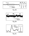
- FIGS. 2A-2G illustrate electrical characterization and bandwidth analysis of certain sensors in another set of embodiments
- FIGS. 3A-3E illustrate monitoring of cells using certain sensors in accordance with some embodiments of the invention
- FIGS. 4A-4D illustrate monitoring of cells using a plurality of sensors, in yet other embodiments of the invention.
- FIGS. 5A-5I schematically illustrate the fabrication of a sensor in accordance with one embodiment of the invention
- FIGS. 6A-6C are images of certain sensors in one set of embodiments.
- FIGS. 7A-7C illustrate data demonstrating certain electrical characteristics of a sensor in one embodiment of the invention
- FIGS. 8A-8B are images of sensors in certain embodiments of the invention.
- FIGS. 9A-9C illustrate the use of a plurality of sensors used in accordance with some embodiments of the invention.
- the present invention generally relates to nanotechnology, including field effect transistors and other devices used as sensors (for example, for electrophysiological studies), nanotube structures, and applications. Certain aspects of the present invention are generally directed to transistors such as field effect transistors, and other similar devices.
- a field effect transistor is used where a nanoscale wire, for example, a silicon nanowire, acts as a transistor channel connecting a source electrode to a drain electrode. In some cases, a portion of the transistor channel is exposed to an environment that is to be determined, for example, the interior or cytosol of a cell.
- a nanotube or other suitable fluidic channel may be extended from the transistor channel into a suitable environment, such as a contained environment within a cell, so that the environment is in electrical communication with the transistor channel via the fluidic channel.
- the rest of the transistor channel may be coated, e.g., so that the electrical properties of the transistor channel reflect the electrical behavior of the environment that the fluidic channel is in communication with.
- Other aspects of the invention are generally directed to methods of making such sensors, methods of using such sensors, kits involving such sensors, or the like.
- one aspect of the invention is generally directed to sensors including transistors such as field effect transistors, or other suitable devices, for detecting a condition within an environment that is external to the sensor.
- the environment may be one that is contained, for example, inside an interface.
- the environment may be an environment contained within an emulsion droplet, a micelle, a liposome, a cell, or the like.
- the contained environment may have a volume of less than about 1 ml, less than about 100 microliters, less than about 10 microliters, less than about 1 microliter, less than about 100 nanoliters, less than about 10 nanoliters, or less than about 1 nanoliter.
- the sensor may include one or more fluidic channels that can be introduced to the environment external to the sensor such that the sensor is in electrical, chemical, and/or physical communication with the environment.
- the environment is a contained environment that is the fluidic channel is in communication with, although the contained environment may not physically contact other components of the sensor.
- a cell may be contained in an extracellular fluid, and a sensor may be positioned such that the fluidic channel is in communication with the cytosol within the cell (i.e., the contained environment), while the rest of the sensor is in physical contact only with the extracellular fluid and/or the plasma membrane that defines the “interface” or external boundary of the cell.
- a field effect transistor 30 is formed from source electrode 35 , drain electrode 37 , and transistor channel 25 connecting the source electrode 35 to drain electrode 37 .
- transistor channel 25 is formed from a p-doped silicon nanowire (“SiNW”).
- SiNW silicon nanowire
- Other nanoscale wires may be used in other embodiments, however, although a silicon nanowire is shown here as an illustrative example.
- nanotube 10 Connected to a portion of transistor channel 25 is nanotube 10 , which functions as a fluidic channel in this example.
- Fluid from an environment to be sensed, for example, cytosol (intracellular fluid) 15 within cell 20 may be able to at least partially enter nanotube 10 and in some cases, come into contact with a portion of transistor channel 25 .
- transistor channel 25 is in electrical, chemical, and/or physical communication with cytosol 15 in the interior of cell 20 .
- the interior of cell 20 i.e., the cytosol
- the interior of cell 20 defines a contained environment that is in contact with field effect transistor 30 via nanotube 10 .
- the other components of field effect transistor 30 do not directly physically contact cytosol 15 in the interior of cell 20 , although these components are in contact with extracellular fluid 39 in this example. In other embodiments, some or all of these components may also come into contact with the plasma membrane 21 of cell 20 , although even then, these components would not come into contact with cytosol 15 in the interior of cell 20 . Accordingly, as shown in this example, the sensor is able to communicate with an environment that is contained inside an interface via a fluidic channel.
- coating material 18 (SiO 2 in this example) is used.
- coating material 18 may be positioned on transistor channel 25 such that transistor channel 25 can be controlled by electrical, chemical, and/or physical interactions with the contained environment, e.g., with cytosol 15 , instead of electrical, chemical, and/or physical interactions with extracellular fluid 39 .
- coating material 18 may be chosen to be substantially nonconductive, and/or coating material 18 may be substantially chemically inert relative to extracellular fluid 39 , such that substantially no chemical reactions or physical interactions between extracellular fluid 39 and transistor channel 25 can occur that could affect the functioning of transistor channel 25 .
- a fluidic channel extending into cytosol 15 in the interior of cell 20 may be defined by a nanotube 10 formed, at least in part, out of the coating material, e.g., so that extracellular fluid 39 does not have any substantial electrical, chemical, and/or physical interactions with the interior of nanotube 10 .
- a fluidic channel of the sensor may be inserted into a first, contained environment that is surrounded by a second environment.
- a contained environment may be defined as the interior of a cell, an emulsion droplet, a micelle, a liposome, etc.
- the second, surrounding environment may be any fluid separate from and containing the containing environment, for example, water, an aqueous fluid, an organic fluid or the like.
- a sensor or other apparatus may include a transistor such as a bipolar junction transistor or a metal electrode.
- a nanotube or other fluidic channel may be fabricated as part of an electrode or a logic gate, which can be used as a sensor or other apparatus as discussed herein.
- the sensor may be used to determine a suitable environment, such as a contained environment.
- the senor or other apparatus may be placed in electrical, chemical, and/or physical communication with the environment, such that an appropriate electrical, chemical, and/or physical property can be determined by a sensor and/or so that an electrical, chemical, or other physical property may be affected by an apparatus.
- Determine generally refers to the analysis of a species, for example, quantitatively or qualitatively, and/or the detection of the presence or absence of the species. “Determining” may also refer to the analysis of an interaction between two or more species, for example, quantitatively or qualitatively, and/or by detecting the presence or absence of the interaction.
- Non-limiting examples of suitable electrical properties that may be determined or altered include charge, conductance, impedance, resistance, voltage (e.g., with respect to fluid externally of the cell, ground, etc.), current, potential, or the like.
- a recognition entity to an analyte suspected of being contained in the environment may be placed in the sensor, e.g., so that the sensor is able to determine the analyte within the solution, for example, through changes in electrical properties. Additional details are discussed below, as well as in U.S. Pat. No. 7,129,554, issued Oct. 31, 2006, entitled “Nanosensors,” by Lieber, et al., incorporated herein by reference in its entirety.
- a field effect transistor may be used in the sensor or other apparatus.
- the field effect transistor can include a source electrode, a drain electrode, and an electrical connector, such as a nanoscale wire, electrically connecting the source electrode to the drain electrode.
- the electrical connector may thus act as a transistor channel within the field effect transistor, and may be formed from any suitable material able to electrically connect the source electrode to the drain electrode.
- the electrical connector may be, for example, a nanoscale wire or a larger wire, for instance, an electrical line, a microscale wire, a planar substrate, graphene, or the like.
- the electrical connector may be embedded in a substrate, or free-standing in some embodiments. In one set of embodiments, the electrical connector may be substantially cylindrical.
- a sensor or other apparatus includes an electrode, for example, containing a fluidic channel or as part of a transistor such as a field effect transistor
- the electrodes may be formed out of any suitable material. If more than one electrode is present, the electrodes may be formed out of the same or different materials.
- the electrodes are formed from metals (e.g., deposited on a surface using known techniques, such as photolithography).
- suitable electrode materials include silicon, or metals such as gold, silver, copper, zinc, cadmium, iron, nickel, cobalt, palladium, platinum, etc.
- the electrical connector includes a nanoscale wire.
- the nanoscale wire may include one or more nanowires or nanotubes. Typically, nanowires are solid while nanotubes are hollow, as discussed below.
- the nanoscale wire may be formed out of any suitable electrically conductive material, for example, a carbon nanotube, a semiconductor nanowire, a ZnO nanowire, graphene (e.g., a graphene ribbon), a metal nanowire, or the like, and may have any suitable dimensions. Other examples of suitable materials are discussed in detail below.
- a nanoscale wire within the sensor or other apparatus may have an average cross-sectional diameter of less than about 5 micrometers and/or a length of less than about 1 micrometer.
- the nanoscale wire may have a cross-sectional diameter of less than about 5 micrometers, less than about 3 micrometers, less than about 1 micrometer, less than about 800 nm, less than about 600 nm, less than about 400 nm, less than about 200 nm, less than about 100 nm, less than about 80 nm, less than about 60 nm, less than about 40 nm, less than about 20 nm, less than about 10 nm, or less than about 5 nm.
- the diameter may be at least about 2 nm, at least about 5 nm, at least about 10 nm, at least about 20 nm, or at least about 50 nm.
- the inner diameter or the outer diameter may have any of these dimensions, and these dimensions may be independently chosen.
- the nanotube may have an inner diameter of 50 nm and an outer diameter of 150 nm.
- the nanoscale wire may have a length of at least about 10 nm, at least about 30 nm, at least 50 nm, at least about 100 nm, at least about 300 nm, at least about 500 nm, at least about 1 micrometer, at least about 3 micrometers, at least about 5 micrometers, at least about 10 micrometers, at least about 30 micrometers, at least about 50 micrometers, at least about 100 micrometers, at least about 300 micrometers, at least about 500 micrometers, or at least about 1 mm.
- the nanoscale wire may have a length of less than about 1 micrometer, less than about 800 nm, less than about 600 nm, less than about 400 nm, less than about 200 nm, or less than about 100 nm.
- a sensor or other apparatus comprising the nanoscale wire(s) may have maximum dimensions no greater than the ones described in this paragraph.
- an apparatus is used to deliver a current or a potential to an environment such as a contained environment, and in certain embodiments, a sensor is used to determine an electrical, chemical, and/or physical property of the environment. In some cases, the same device may be used to both determine and alter an environment.
- a sensor or other apparatus may be used that may be able to determine and/or apply an (absolute) electric potential of greater than about 0.1 microvolts, greater than about 1 microvolt, greater than about 10 microvolts, greater than about 100 microvolts, greater than about 1 millivolt, greater than about 10 millivolts, greater than about 100 millivolts, greater than about 1 volt, or even greater.
- the nanoscale wire may detect an electric potential between about 0.1 microvolts and 1 volt, between about 0.1 microvolts and about 100 microvolts, between about 10 microvolts and about 10 millivolts, or between about 1 millivolt and about 1 volt.
- the potential may be positive or negative.
- the intracellular potential of a cell may be held to be between about ⁇ 40 millivolts and ⁇ 100 millivolts, between about ⁇ 60 millivolts and ⁇ 90 millivolts, between about ⁇ 50 millivolts and ⁇ 80 millivolts, or between about ⁇ 40 millivolts and ⁇ 60 millivolts, etc.
- the nanoscale wire may determine and/or apply a current greater than about 0.1 picoamps, greater than about 1 picoamp, greater than about 10 picoamps, greater than about 100 picoamps, greater than about 1 nanoamp, greater than about 10 nanoamps, greater than about 100 nanoamps, greater than about 1 microamp, greater than about 10 microamps, greater than about 100 microamps, greater than about 1 milliamp, greater than about 10 milliamps, greater than about 100 milliamps, greater than about 1 amp, or even more.
- the nanoscale wire transmit a current between about 0.1 picoamps and about 100 microamps, between about 0.1 picoamps and about 100 picoamps, between about 10 picoamps and about 10 nanoamps, between about 1 nanoamp and 1 microamp, or between about 100 nanoamps and about 100 microamps.
- the nanoscale wire may, in some embodiments, perform as a transistor channel in the transistor.
- the nanoscale wire may allow, for example, an increase or decrease in the flow of current between the source and drain of the transistor in response to a threshold electrical potential, e.g., as is controlled via interaction with the nanoscale wire and a fluid within the fluidic channel.
- the interaction may be, e.g., an electrical, chemical, and/or physical interaction.
- the threshold electrical potential may be within any of the voltage ranges listed above.
- fluid within the fluidic channel may be able to access at least a portion of the nanoscale wire, e.g., causing an electrical, chemical, and/or physical interaction with the nanoscale wire.
- this interaction may allow the nanoscale wire to function as a transistor channel in a field effect transistor, or other device as is discussed herein.
- the fluidic channel is defined by one or more nanotubes (which are hollow), or other structure able to contain a fluid.
- Examples of such structures include, without limitation, a microfluidic chamber, a microfluidic channel, a structure having a bowl shape, or the like.
- the nanotube may be positioned such that one end of the nanotube is closed by the nanoscale wire. A non-limiting example of such a configuration is shown in FIG. 1A .
- the nanotube may be formed out of any suitable material.
- the fluidic channel may comprise a conductive material, a non-conductive material, a semiconductive material, or the like, or combinations thereof.
- the nanotube does not need to play a role in any electrical, chemical, and/or physical interactions between the fluid and the nanoscale wire (e.g., a transistor channel for a field effect transistor).
- the fluidic channel may simply channel fluid between the environment and the nanoscale wire at the bottom of the fluidic channel.
- the fluidic channel does not have to be electrically conductive (although it can be in some embodiments), and the fluidic channel may be formed out of any suitable material able to channel a fluid, including non-conductive or semiconductive materials, as well as conductive materials.
- the nanotube may have an electrical conductivity less than that of a semiconductive carbon nanotube having substantially the same dimensions as the nanotube.
- suitable materials that the fluidic channel can comprise include oxides such as metal oxides (for example, SiO 2 , Al 2 O 3 , TiO 2 , HfO 2 , ZnO 2 , etc.); metals (e.g., Au, Pt, Cu, Ag, etc.), or the like.
- the fluidic channel may include one or more carbon nanotubes.
- the nanotube may have any of the dimensions for nanotubes described herein.
- a coating material may be present on at least a portion of a fluidic channel and/or a nanoscale wire, e.g., that is used as a transistor channel for a field effect transistor.
- the coating material may be selected to be substantially electrically nonconductive, and/or substantially chemically inert relative to a surrounding environment, e.g., such that substantially no chemical reactions or physical interactions between the surrounding environment and the underlying portions can occur.
- the coating material may be selected to be substantially electrically nonconductive such that the electrical properties of the nanoscale wire is controlled by the electrical properties of fluid contained within the fluidic channel, rather than the electrical behavior of the environment external of the fluidic channel.
- the coating material may be formed out of any suitable material.
- the coating material may be have the same composition as the nanotubes described above, although in other embodiments, the coating material may have a different composition.
- suitable materials that can be used as coating materials include oxides such as metal oxides (for example, SiO 2 , Al 2 O 3 , TiO 2 , HfO 2 , ZnO 2 , etc.); metals (e.g., Au, Pt, Cu, Ag, etc.), or the like, depending on the application.
- a fluidic channel may be positioned to be substantially perpendicular to a nanoscale wire, e.g., as is shown in FIG. 1A for a nanotube.
- the fluidic channel need not be positioned at a right angle, and can be positioned at any other suitable angle.
- the angle of the fluidic channel with respect to the underlying nanoscale wire (and/or other electrical connector) may be, for example, at least about 30°, at least about 45°, at least about 60°, at least about 65°, at least about 70°, at least about 75°, at least about 80°, or at least about 85°, etc.
- the field effect transistor may be positioned on the surface of a substrate, for example, of a chip, such as a silicon wafer.
- a chip such as a silicon wafer.
- the chip may include one or more sensors or other apparatuses such as those discussed herein, and the sensors or other apparatuses may be positioned on the surface of the substrate using various techniques for semiconductor device fabrication known to those of ordinary skill in the art, for example, photolithography, ion implantation, etching, chemical vapor deposition, physical vapor deposition, molecular beam epitaxy, or the like. Any number of sensors and/or other apparatuses may be present, and they may each be independently the same or different.
- a plurality of sensors and/or other apparatuses may be used for determining a cell or a plurality of cells, or other applications such as those discussed herein.
- the nanoscale wires may be positioned on (or formed in the substrate), with some or all of the nanotubes (or other fluidic channels) positioned substantially perpendicularly relative to the substrate, or at other angles such as those described above.
- sensors and/or other apparatuses such as those described herein may be prepared by preparing a branched nanoscale wire, coating the branched nanoscale wire with a coating material, and etching a portion of the coating material and/or the branched nanoscale wire to form a fluidic channel.
- the branched nanoscale wire may be heterogeneous, for instance, defining a first portion susceptible to etching and a second portion that is relatively more resistant to etching (although some etching may still occur, at least in certain embodiments). In other embodiments, however, other methods may be used to form a sensor and/or other apparatus.
- a nanotube such as a carbon nanotube
- a nanoscale wire e.g., using atomic layer deposition, chemical vapor deposition, physical vapor deposition, water-assisted chemical vapor deposition, or the like.
- Other fluidic channels such as microfluidic chambers or microfluidic channels, may also be grown, e.g., using techniques such as photolithography, bulk or surface micromachining, replication techniques (embossing, printing, casting and injection molding), nuclear track or chemical etching, etc.
- FIG. 5A illustrates a SiNW deposited on the surface of a substrate (e.g., a chip), and FIG. 5B shows the positioning of a gold nanoparticle on a specific location on the SiNW.
- SiNW and gold are discussed here as non-limiting examples; as discussed elsewhere herein, other materials may also be used instead of and/or in addition to SiNW or gold.
- a germanium nanowire (“GeNW”) is grown to be substantially perpendicular to the SiNW, using the nanoparticles to facilitate this reaction, as discussed herein.
- metal contacts are deposited or defined on the substrate, e.g., as source and drain electrodes, then the entire structure is coated with a coating material, for example, SiO 2 .
- a coating material for example, SiO 2 .
- One technique that can be used for coating is atomic layer deposition (“ALD”).
- a photoresist may be added to cover the substrate and the structures thereon such that only a portion of the GeNW remains above the surface of the photoresist.
- the photoresist can be exposed to an etchant (e.g., buffered hydrofluoric acid) to remove the portion of the coating material above the surface of the photoresist.
- an etchant e.g., buffered hydrofluoric acid
- the photoresist and the GeNW may then be removed by exposure to one or more suitable etchants, e.g., photoresist remover and hydrogen peroxide (H 2 O 2 ).
- suitable etchants e.g., photoresist remover and hydrogen peroxide (H 2 O 2 ).
- Substantially all of the GeNW can be removed, thereby leaving behind a hollow nanotube structure, which can define a fluidic channel that contacts the original SiNW.
- suitable etchants e.g., photoresist remover and hydrogen peroxide (H 2 O 2 ).
- H 2 O 2 hydrogen peroxide
- a first nanoscale wire is provided and a second nanoscale wire is grown to be in contact with the first nanoscale wire, e.g., using techniques such as those discussed herein.
- Each of the nanoscale wires may independently be, for example, a solid nanowire, a nanotube, etc., as discussed herein.
- the contact may be, for example, end-on (e.g., forming a “T” structure, as is shown in FIG. 1 ), and the angle of contact may be 90° or any other angle discussed herein. In some embodiments, however, the contact need not be end-on.
- the nanoscale wires may cross at their middles (e.g., forming an “X” structure”).
- any suitable technique for growing the second nanoscale wire to be in contact with the first nanoscale wire may be used.
- the second nanoscale wire is first grown, then brought to be in contact with the first nanoscale wire; in other embodiments, however, the second nanoscale wire may be directly grown from the first nanoscale wire.
- Non-limiting examples of techniques for growing the first nanoscale wire and/or the second nanoscale wire include vapor-liquid-solid growth techniques, laser assisted catalytic growth, catalytic chemical vapor deposition, solution based growth, chemical vapor deposition, or the like. Further techniques may be seen, for example, in U.S. patent application Ser. No. 09/935,776, filed Aug.
- any catalyst able to catalyze the production of nanoscale wires may be used, depending on the technique used to produce the nanoscale wire, e.g., as catalyst nanoparticles.
- a wide range of materials may be used as the catalyst nanoparticle in these embodiments, for example, a transition metal such as gold, silver, copper, zinc, cadmium, iron, nickel, cobalt, palladium, platinum, aluminum, or the like.
- the first nanoscale wire and/or the second nanoscale wire may be coated with a coating material, using any suitable technique known to those of ordinary skill in the art for coating, for example, via atomic layer deposition, chemical vapor deposition, physical vapor deposition, casting, or the like.
- Any coating material may be used, for instance, oxides such as metal oxides (for example, SiO 2 , Al 2 O 3 , TiO 2 , HfO 2 , ZnO 2 , etc.); metals (e.g., Au, Pt, Cu, Ag, etc.), or the like.
- the coating material may be at least partially blocked, for example, by applying a photoresist or another suitable blocking material that can be later removed to the first nanoscale wire and/or the second nanoscale wire.
- a photoresist or another suitable blocking material that can be later removed to the first nanoscale wire and/or the second nanoscale wire.
- the photoresist may be applied to substantially cover the first nanoscale wire and/or the second nanoscale wire.
- the photoresist may be applied such that only the end of the second nanoscale wire is not covered by photoresist.
- photoresists known to those of ordinary skill in the art may be used, depending on the application (e.g., poly(methyl methacrylate), poly(methyl glutarimide), phenol formaldehyde resin, SU-8 (Microchem Corp., Newton, Mass.), S1805, S1813, S1818, etc.).
- a portion of the coating material, e.g., on the uncovered tip of the second nanoscale wire may be removed, e.g., using an etchant or other technique able to remove the uncovered portion of the coating material, for example, reactive ion etching.
- etchants potentially suitable for removing coating materials include HCl, HF, NH 4 F or the like, and may be readily selected by those of ordinary skill in the art based on the selection of the coating material.
- the photoresist or another suitable blocking material may also be removed, e.g., by using etching, or another suitable removal technique.
- an etchant may etch the photoresist while not substantially etching the coating material, e.g., such that sufficient coating material remains to coat the first nanoscale wire and/or form a nanotube or other fluidic channel after exposure to the etchant.
- the photoresist may be substantially completely removed by the etchant, while only a portion of the coating material is removed.
- the second nanoscale wire may also be removed, e.g., by etching or another suitable technique.
- the etchant may be chosen to be able to remove the second nanoscale wire without substantially etching away other components of the device, and may be selected based on the choice of materials used for the device by those of ordinary skill in the art.
- the second nanoscale wire may be removed, for example, by heating the device to drive off the carbon nanotube, e.g., as CO 2 .
- etchants examples include, but are not limited to e.g., H 2 O 2 , KOH, I 2 /KI, ethylene diamine and pyrocatechol, iron chloride, plasmas such as CCl 4 or CF 4 plasma, tetramethylammonium hydroxide, or the like.
- branched nanoscale wires are used in accordance with certain aspects of the invention. See, e.g., U.S. patent application Ser. No. 12/310,764, filed Mar. 6, 2009, entitled “Branched Nanoscale Wires,” by Lieber, et al., published as U.S. Patent Application Publication No. 2011/0042641 on Feb. 24, 2011, incorporated herein by reference in its entirety.
- nanoparticles such as gold nanoparticles
- the nanoscale wire may be, for example, a semiconductor nanoscale wire, a nanoscale wire having a core and a shell, etc.
- gold nanoparticles are deposited onto the nanoscale wire by etching the nanoscale wire using, for example, HF, to produce an H-terminated surface.
- the H-terminated surface in certain cases, causes the electrochemical reduction of gold ions in solution, for example, from a charged state (e.g., Au 2+ or Au 3+ ) to a neutral (i.e., Au 0 ) state, i.e., such that the gold ions precipitate out of solution to form nanoparticles on the surface of the H-terminated surface.
- the size of the deposited gold nanoparticles may be controlled, for instance, by controlling the concentration of gold in solution, and/or by controlling the deposition or exposure time.
- nanoparticle typically, only one nanoparticle is attached to the surface of a nanoscale wire, and the nanoparticle may be used as a blocking material to block coating of the nanoscale wire with the coating material at that particular location.
- the location may then be used to grow a nanoscale wire thereon, e.g., as discussed herein.
- two, three, four, or more nanoparticles may be attached to the surface of a nanoscale wire, e.g., to produce a device having a nanoscale wire and a plurality of nanotubes.
- some or all of the nanotubes may be positioned such that one end of the nanotube physically contacts a side of the nanoscale wire. In other embodiments, however, the nanotubes may contact the nanoscale wire in other ways, e.g., contacting at their middles.
- segments of material may be grown from them, e.g., to form a nanowire.
- CVD chemical vapor deposition
- VLS vapor-liquid-solid growth techniques
- segments of material for example, to produce segments comprising semiconductors such as Si, GaAs, GaP, InP, CdSe, ZnSe, CdS, ZnS, etc.
- solution-phase synthesis techniques may be used.
- gold segments may be grown from nanoparticles by annealing the nanowire/nanoparticle composite and exposing the nanoparticles to a solution containing gold (for example, gold tetrachloride acid, HAuCl 4 ).
- gold for example, gold tetrachloride acid, HAuCl 4
- surfactants such as cetyl trimethyl ammonium bromide (CTAB) may preferentially interact with the ⁇ 100 ⁇ and ⁇ 111 ⁇ facets of the gold nanoparticle, and thus, growth occurs primarily along the ⁇ 110> direction, causing uniaxial elongation.
- branched nanoscale wires having at least first segment having a first composition and a second segment having a second composition different from the first composition may be produced.
- the second segment may be formed to be a sacrificial template that is to be removed, e.g., by etching, heating, laser ablation, etc.
- one or more of the segments of the branched nanoscale wire comprises a semiconductor, for example, a Group IV semiconductor, a Group III-V semiconductor, a Group II-VI semiconductor, or the like. Examples include, but are not limited to, Si, GaAs, GaP, InP, CdSe, ZnSe, CdS, ZnS, etc. If more than one segment comprising a semiconductor is present, the segments may each independently be the same or different. As a non-limiting example, if one segment is Si, another segment within the branched nano scale wire may be GaAs, GaP, InP, CdSe, ZnSe, CdS, and/or ZnS. Combinations of these and/or other semiconductors are also possible, for example, a branched nanoscale wire may have three or more types of semiconductors, such as Si/GaAs/GaP, Si/GaAs/InP, etc.
- one or more nanoparticles may be deposited onto a nanoscale wire by producing a charge on the nanoscale wire, and exposing the charged nanoscale wire to at least one nanoparticle having an opposite charge to the charged nanoscale wire.
- the nanoscale wire may be, for example, a semiconductor nanoscale wire, a nanoscale wire having a core and a shell, a branched nanoscale wire (e.g., produced as described herein), etc.
- the charge on the nanoscale wire may be produced, for instance, electrically, by immobilizing a charged entity to the nanoscale wire, etc.
- a positively-charged entity may first be immobilized to the nanoscale wire.
- the positively-charged entity can be, for instance, a positively-charged polymer such as poly(lysine), poly(ethyleneimine), or poly(allylamine hydrochloride).
- the nanoparticles can then be attracted to the positively-charged entity and thereby become adsorbed onto the nanoscale wire.
- segments can then be grown from the nanoparticles to produce a branched nanoscale wire.
- a surface of the nanoscale wire is treated to produce a reducing surface, i.e., a surface that can reduce a positive ion, and the reducing surface is then exposed to an ionic solution, whereby an ion in solution can be reduced by the reducing surface. If the ions are reduced to a 0 state, the ions may precipitate out of solution, e.g., forming nanoparticles on the reducing surface of the nanoscale wire.
- the reducing surface can be prepared, for example, by etching the nanoscale wire with an etching solution.
- An example of an etching solution is HF, which causes the surface to become H-terminated.
- Other examples include NH 4 F or NH 4 F/HF.
- Exposure of the H-terminated surface to positively-charged metal ions in solution can cause the reduction of the metal ions ultimately to a zero charge, which may thus cause precipitation of the metal ions from solution, e.g., to form nanoparticles.
- the metal is more electronegative than hydrogen.
- gold ions in solution e.g., Au 3+ or Au 2+
- Au 0 gold tetrachloride acid
- HAuCl 4 gold tetrachloride acid
- silver ions in solution e.g., Ag +
- Ag + silver ions in solution
- a non-limiting example of a solution containing silver ions is AgNO 3 .
- suitable metals include Pd, Pt, or Cu.
- the size and/or density of the deposited nanoparticles may be controlled by, e.g., the concentration of metal ions in solution, and/or the exposure time.
- additional segments e.g., comprising a semiconductor and/or a metal
- semiconductor segments can be grown from the nanoparticles using conventional techniques such as CVD (chemical vapor deposition) or other various vapor-liquid-solid (VLS) growth techniques.
- CVD chemical vapor deposition
- VLS vapor-liquid-solid
- certain arrangements may utilize metal-catalyzed CVD techniques (“chemical vapor deposition”) to synthesize segments.
- CVD synthetic procedures can readily be carried out by those of ordinary skill in the art.
- the segments may also be grown through laser catalytic growth. If uniform diameter nanoparticles (less than 10% to 20% variation depending on how uniform the nanoparticles are) are used as the catalytic cluster, segments with uniform size (diameter) distribution can be produced, where the diameter of the segments is determined by the size of the nanoparticles. By controlling growth time, segments with different lengths can be grown.
- C-CVD catalytic chemical vapor deposition
- reactant molecules are formed from the vapor phase.
- Nanoscale wires may be doped by introducing the doping element into the vapor phase reactant (e.g. diborane and phosphane).
- the doping concentration may be controlled by controlling the relative amount of the doping compound introduced in the composite target.
- the final doping concentration or ratios are not necessarily the same as the vapor-phase concentration or ratios. By controlling growth conditions, such as temperature, pressure or the like, segments having the same doping concentration may be produced.
- nanoscale wires of any of a variety of materials may be grown directly from vapor phase through a vapor-solid process.
- metal segments can be grown in a solution-phase synthesis technique from the nanoparticles, by exposing the nanoparticles to a solution containing a metal ion.
- the metal ion may be the same or different than the metal in the nanoparticles.
- deposition of the metal ions on the nanoparticle can be constrained due to the presence of surfactants or other species that preferentially interact with certain faces of the nanoparticle, and thus, growth in certain directions may be preferred.
- the nanoparticle is gold
- deposition of gold onto the nanoparticle may be constrained and growth along the ⁇ 110> axis of the deposited gold nanoparticle may be preferred, leading to uniaxial elongation.
- a surfactant such as cetyl trimethyl ammonium bromide (CTAB) may preferentially interact with the ⁇ 100 ⁇ and ⁇ 111 ⁇ facets of a gold nanoparticle, causing growth to occur primarily along the ⁇ 110> axis.
- CTAB cetyl trimethyl ammonium bromide
- the diameter and/or the aspect ratio may be controlled by controlling, for example, the concentration of metal ion in solution, and/or the acidity or pH, i.e., the hydrogen ion concentration.
- metals that can be used include, but are not limited to, noble metals such as gold, silver, copper, zinc, cadmium, iron, nickel, cobalt, palladium, platinum, or the like.
- a sensor may be used to determine environments such as contained environments, e.g., an environment contained inside an interface.
- An interface may divide a contained environment from a surrounding environment.
- the interface may, in some embodiments, be defined as a specific material, for example, by an amphiphilic material (e.g., a phospholipid or a surfactant).
- the interface is a lipid bilayer.
- an interface may be defined as a phase boundary between two substantially immiscible phases; for example, the interface may be formed by oil-water mixture, such as in an emulsion.
- the environment to be determined by the sensor may be a contained environment contained within an emulsion, a fluidic droplet, a micelle, a liposome, a cell (such as an electrogenic cell, i.e., one that exhibits electrical activity, such as a neuron or a cardiac cell), or any entity having an interface that is able to define an internal contained environment.
- a cell such as an electrogenic cell, i.e., one that exhibits electrical activity, such as a neuron or a cardiac cell
- the cell may be an isolated cell or may be part of a group of cells, such as in a tissue or biofilm.
- the cell may be any suitable cell, e.g., a human cell, an animal cell, a non-human mammalian cell, a bacterial cell, a eukaryotic cell, or an archaeal cell.
- Non-limiting examples of cells include neurons, cardiomyocytes, muscle cells, and pancreatic beta cells.
- the surrounding environment that surrounds the contained environment may include, for example, a liquid (e.g., cytosol, water, an aqueous fluid, an organic fluid, etc.) and/or a gas, and can be readily chosen or determined by those of ordinary skill in the art.
- a nanoscale wire or other electrical connector in contact with an interface may be used to communicate with the interior environment contained by the interface.
- the communication may be, e.g., electrical, chemical, and/or physical communication.
- the nanoscale wire or other electrical connector may be capable of sending and/or receiving an electrical current, and/or passing an electrical current through the nanoscale wire and through a fluidic channel into the contained environment.
- the contained environment may be probed to determine a property, such as an electrical property, of the contained environment.
- a sensor may be used to determine an electrical property of the contained environment.
- the sensor may, in some embodiments, determine an electrical property, such as conductance, charge, impedance, resistance, voltage (e.g., with respect to fluid externally of the cell, ground, etc.), current, potential, or the like in the contained environment.
- the senor may be used to determine other properties of the contained environment, for example, a chemical, and/or physical in the contained environment.
- an electrical property of the sensor may be correlated with a chemical, and/or physical property within the contained environment.
- the signal corresponding to a first property i.e., electrical potential or electrical current
- the electrical potential determined by a sensor may be correlated with pH, concentration of an analyte, ionic concentration, fluid viscosity, or the like.
- a reaction entity can be used, e.g., contained within a surface of the fluidic channel, such as on a nanotube wall and/or on a nanoscale wire or other electrical connector, and interaction between a binding partner (for example, an analyte) and the reaction entity may produce a determinable change in an electrical property of the electrical connector, which can be determined to determine a chemical, and/or physical in the contained environment.
- a binding partner for example, an analyte
- a nanotube or other fluidic channel may be used to directly access the contained environment, while other portions of the device do not come into physical contact with the contained environment.
- a fluid within the contained environment may come into physical contact with a nanoscale wire within a device (e.g., a transistor channel) via a fluidic channel such that the nanoscale wire is in electrical communication with the fluid.
- Other portions of the nanoscale wire or the device e.g., the electrodes
- Such a device can be used, for example, as a sensor to sense an electrical state of the contained environment, to apply an electrical signal to the contained environment, or the like.
- the fluidic channel may be inserted into the contained environment using any suitable technique, e.g., mechanically (for example, using a micromanipulator or a micropipette).
- the fluidic channel is inserted using mechanical force.
- the fluidic channel and/or the interface may be manipulated such that the fluidic channel and the interface are brought into contact.
- a cell may be manipulated, e.g., using a micromanipulator or a micropipette, and brought into contact with the fluidic channel.
- energy e.g., applying a force to an object such that the object displaces along a vector.
- substantially less energy may be required for a fluidic channel to be inserted through the interface.
- relatively favorable chemical interactions may occur between the fluidic channel and the interface defining the contained environment.
- a fluidic channel may be treated, i.e., chemically, to facilitate entry through the interface into the contained environment.
- a fluidic channel may spontaneously penetrate the interface defining the contained environment, e.g., due to a material present on at least a portion of the fluidic channel.
- Non-limiting examples of such materials include amphiphilic materials include phospholipids, such as phosphatidate, phosphatidylethanolamine, phosphatidylcholine, phosphatidylserine, phosphatidylinositol, phosphatidylinositol phosphate, phosphatidylinositol bisphosphate, and phosphatidylinositol triphosphate, surfactants, polymers, proteins, and polysaccharides.
- phospholipids such as phosphatidate, phosphatidylethanolamine, phosphatidylcholine, phosphatidylserine, phosphatidylinositol, phosphatidylinositol phosphate, phosphatidylinositol bisphosphate, and phosphatidylinositol triphosphate, surfactants, polymers, proteins, and polysaccharides.
- the material may be coupled to the fluidic channel using functional cross-linkers, such as homobifunctional cross-linkers, comprising homobifunctional NHS esters, homobifunctional imidoesters, homobifunctional sulfhydryl-reactive linkers, difluorobenzene derivatives, homobifunctional photoactive linkers, homobifunctional aldehyde, bis-epoxides, homobifunctional hydarzide etc.; heterobifuntional cross-linkers; or trifuntional cross-linkers, or the like.
- functional cross-linkers such as homobifunctional cross-linkers, comprising homobifunctional NHS esters, homobifunctional imidoesters, homobifunctional sulfhydryl-reactive linkers, difluorobenzene derivatives, homobifunctional photoactive linkers, homobifunctional aldehyde, bis-epoxides, homobifunctional hydarzide etc.; heterobifuntional cross-
- a fluidic channel may be capable of interacting (e.g., chemically) with an interface, e.g., defining a contained environment, such as in a cell, liposome, or the like.
- a fluidic channel may contact the interface and fuse with a portion of the interface.
- fuse means that the nanotube integrates into the interface (e.g., a lipid bilayer) such that the lipid bilayer (or other interface) forms a continuous phase around one or more portions of the fluidic channel.
- the lipid bilayer or other interface may rearrange around at least a portion of the fluidic channel, thereby allowing entry of the fluidic channel to occur into the contained environment.
- a portion of the fluidic channel when a fluidic channel interacts with an interface, a portion of the fluidic channel may extend completely through the interface.
- a nanotube may penetrate a cell membrane such that a portion of the nanotube is in contact with the cytosol (or intracellular fluid) inside of the cell.
- a nanotube or other fluidic channel may penetrate more than one interface, e.g., more than one lipid bilayer.
- a nanotube may penetrate the cell membrane of a cell and another membrane inside the cell (e.g., the membrane of an organelle), or a fluidic channel may be used to penetrate a double emulsion droplet, etc.
- cells may be cultured near the nanotubes, and in some cases, the cells may spontaneously uptake at least a portion of the nanotube.
- Non-limiting examples of applications include the study of cells, e.g., electrogenic cells, or the screening of drugs or other agents by exposing the drugs or other agents to a plurality of cells, and determining differences in a property (e.g., an electrical, chemical, and/or physical property) of at least some of the cells in response to the drug or other agents.
- the drug or other agent may be one that is drug that is suspected of being able to alter a property, such as an electrical property, of a cell.
- the drug (or other agent) may be suspected of being able to alter electrical communication between a plurality of cells, as is discussed below.
- an assay may be performed where cells are treated with one or more drugs or other agents (e.g., a library of drug candidates), and the effect of the agent, alone or in combination with other agents, known drugs (i.e., pharmaceutical agent), or the like on an electrical, chemical, and/or physical property of a cell may be determined.
- drugs or other agents e.g., a library of drug candidates
- an apparatus may be used to stimulate a response in a contained environment, and/or to communicate with at least a portion of the contained environment.
- the interaction may be, for instance, electrical, chemical, and/or physical.
- an electrical stimulus such as current or voltage
- a chemical may be released from the apparatus through the fluidic channel into the contained environment.
- the application of an electrical stimulus to a cell e.g., current and/or voltage, may induce an action potential within the cell.
- the apparatus may be used to determine electrical activity in a cell.
- the apparatus may be used in certain embodiments instead of (or in addition to) a patch clamp and/or voltage clamp.
- a plurality of such apparatuses as disclosed herein may be used, e.g., to determine an electrical property of a cell (or other contained environment) at more than one location within the cell, and/or to determine an electrical property of a network of cells.
- certain embodiments of the invention are generally directed to substrates comprising a plurality of such apparatuses (e.g., on a substrate), which may be used for various applications such as multiplex assays.
- a plurality of suitable apparatuses can be used to assay a plurality of cells, e.g., essentially simultaneously.
- a plurality of apparatuses may be used to assay a plurality of regions of a cell, e.g., essentially simultaneously.
- Such an assay may be advantageous for determining, for example, how electrical potential inside a cell varies between a first region and a second region.
- the cells may be isolated and/or networked such that the cells are in electrical communication, e.g., via gap junctions or the like.
- a substrate may contain one or more devices as described herein, and cells may be exposed to the substrate, or cultured on the substrate in certain cases.
- the plurality of devices may interface with the cells, for example such that two, there, or more cells have at least partially inserted therein a fluidic channel, such as a nanotube.
- a plurality of apparatuses may be in electrical communication with one or more electrical recording devices, e.g., so that the cells (or network of cells) may be analyzed, e.g., to determine an electrical, chemical, and/or physical property of the cell (or other contained environment).
- the present invention in various aspects, includes nanoscale wires, each of which can be any nanoscale wire, including nanorods, nanowires, nanotubes, nanoribbons, or the like.
- the present invention may also include larger components, e.g., not necessarily of nanoscale dimensions, although the components may have the same compositions as the nanoscale wires disclosed herein.
- a transistor may include an electrical connector that has a cross-sectional diameter of several micrometers, and the electrical connector may comprise any of the materials disclosed below, or elsewhere herein.
- the nanoscale wires may be formed of any suitable material, for example, organic and inorganic conductive and semiconducting polymers, semiconductor components or pathways and the like.
- Other conductive or semiconducting elements that may be used in some instances include, for example, inorganic structures such as Group IV, Group III/Group V, Group II/Group VI elements, transition group elements, or the like, as described below.
- the nanoscale wire or other electrical connector may be made of semiconducting materials such as silicon, indium phosphide, gallium nitride, graphene, and others.
- the nanoscale wires or other electrical connector may also include, for example, any organic, inorganic molecules that are polarizable or have multiple charge states.
- the nanoscale wire or other electrical connector may include various materials, including metals, semiconductors, and optionally dopants.
- nanoscale wires or other electrical connectors may include main group and metal atom-based wire-like silicon, transition metal-containing wires, gallium arsenide, gallium nitride, indium phosphide, germanium, and/or cadmium selenide.
- Other examples include metals such as gold, silver, copper, zinc, cadmium, iron, nickel, cobalt, palladium, platinum, etc.
- the dopant or the nanoscale wire may be an elemental semiconductor, for example, silicon, germanium, tin, selenium, tellurium, boron, diamond, graphene, or phosphorous.
- the dopant or the nanoscale wire (or other electrical connector) may also be a solid solution of various elemental semiconductors.
- Examples include a mixture of boron and carbon, a mixture of boron and P(BP 6 ), a mixture of boron and silicon, a mixture of silicon and carbon, a mixture of silicon and germanium, a mixture of silicon and tin, or a mixture of germanium and tin.
- the dopant or the nanoscale wire may include mixtures of Group IV elements, for example, a mixture of silicon and carbon, or a mixture of silicon and germanium.
- dopant or the nanoscale wire (or other electrical connector) may include a mixture of a Group III and a Group V element, for example, BN, BP, BAs, AlN, AlP, AlAs, AlSb, GaN, GaP, GaAs, GaSb, InN, InP, InAs, or InSb. Mixtures of these may also be used, for example, a mixture of BN/BP/BAs, or BN/AlP.
- dopant or the nanoscale wire may include alloys of Group III and Group V elements.
- the alloys may include a mixture of AlGaN, GaPAs, InPAs, GaInN, AlGaInN, GaInAsP, or the like.
- the dopant or the nanoscale wire (or other electrical connector) may also include a mixture of Group II and Group VI semiconductors.
- the semiconductor may include ZnO, ZnS, ZnSe, ZnTe, CdS, CdSe, CdTe, HgS, HgSe, HgTe, BeS, BeSe, BeTe, MgS, MgSe, or the like.
- Alloys or mixtures of these dopants are also be possible, for example, (ZnCd)Se, or Zn(SSe), or the like. Additionally, alloys of different groups may also be possible, for example, a combination of a Group II-Group VI and a Group III-Group V semiconductor, for example, (GaAs) x (ZnS) 1-x .
- Other examples of dopants or nanoscale wires (or other electrical connectors) may include combinations of Group IV and Group VI elements, such as GeS, GeSe, GeTe, SnS, SnSe, SnTe, PbO, PbS, PbSe, or PbTe.
- Other semiconductor mixtures may include a combination of a Group I and a Group VII, such as CuF, CuCl, CuBr, CuI, AgF, AgCl, AgBr, AgI, or the like.
- Other compounds may include different mixtures of these elements, such as BeSiN 2 , CaCN 2 , ZnGeP 2 , CdSnAs 2 , ZnSnSb 2 , CuGeP 3 , CuSi 2 P 3 , Si 3 N 4 , Ge 3 N 4 , Al 2 O 3 , (Al,Ga,In) 2 (S,Se,Te) 3 , Al 2 CO, (Cu,Ag)(Al,Ga,In,Tl,Fe)(S,Se,Te) 2 and the like.
- a p-type dopant may be selected from Group III, and an n-type dopant may be selected from Group V, for example.
- a p-type dopant may be selected from the group consisting of B, Al and In, and an n-type dopant may be selected from the group consisting of P, As and Sb.
- a p-type dopant may be selected from Group II, including Mg, Zn, Cd and Hg, or Group IV, including C and Si.
- An n-type dopant may be selected from the group consisting of Si, Ge, Sn, S, Se and Te. It will be understood that the invention is not limited to these dopants, but may include other elements, alloys, or materials as well.
- Controlled doping of nanoscale wires or other electrical connectors can be carried out to form, e.g., n-type or p-type semiconductors.
- One set of embodiments involves use of at least one semiconductor, controllably-doped with a dopant (e.g., boron, aluminum, phosphorous, arsenic, etc.) selected according to whether an n-type or p-type semiconductor is desired.
- a dopant e.g., boron, aluminum, phosphorous, arsenic, etc.
- a bulk-doped semiconductor may include various combinations of materials, including other semiconductors and dopants.
- the nanoscale wire (or other electrical connector) may be a semiconductor that is doped with an appropriate dopant to create an n-type or p-type semiconductor, as desired.
- silicon may be doped with boron, aluminum, phosphorous, or arsenic.
- this invention involves controlled doping of semiconductors selected from among indium phosphide, gallium arsenide, gallium nitride, cadmium selenide.
- Dopants including, but not limited to, zinc, cadmium, or magnesium can be used to form p-type semiconductors in this set of embodiments, and dopants including, but not limited to, tellurium, sulfur, selenium, or germanium can be used as dopants to form n-type semiconductors from these materials.
- These materials may define direct band gap semiconductor materials and these and doped silicon are well known to those of ordinary skill in the art.
- the present invention contemplates use of any doped silicon or direct band gap semiconductor materials for a variety of uses.
- Certain aspects of the invention are generally directed to fabricating semiconductor nanoscale wires and other nanoscale objects (or other electrical connectors) such as those described herein.
- Techniques useful for fabricating nanoscale wires or other electrical connectors include, but are not limited to, vapor phase reactions (e.g., chemical vapor deposition (“CVD”) techniques such as metal-catalyzed CVD techniques, catalytic chemical vapor deposition (“C-CVD”) techniques, organometallic vapor phase deposition-MOCVD techniques, atomic layer deposition, chemical beam epitaxy, etc.), solution phase reactions (e.g., hydrothermal reactions, solvothermal reactions), physical deposition methods (e.g., thermal evaporation, electron-beam evaporation, laser ablation, molecular beam epitaxy), vapor-liquid-solid (“VLS”) growth techniques, laser catalytic growth (“LCG”) techniques, surface-controlled chemical reactions, or the like, for instance, as disclosed in Ser.
- CVD chemical vapor deposition
- C-CVD cat
- nanoscale Wires and Related Devices may be either grown in place or deposited after growth.
- the nanoscale wires or other electrical connectors may be grown on a substrate using techniques such as photolithography, e.g., using conventional photolithography, submicron photolithography, extreme-UV lithography or nanoimprint lithography.
- a nanoscale wire containing one or more kinks can be grown using certain vapor-liquid-solid (“VLS”) growth techniques.
- VLS vapor-liquid-solid
- a catalyst particle may be used to grow a first portion of a nanoscale wire, for instance, by exposing the catalyst particle to a first reactant, such as a gaseous reactant.
- a first reactant such as a gaseous reactant.
- Such a wire may be axially extended in a first direction. Exposure of the catalyst particle to the first reactant may then be stopped, which may stop axial growth of the wire.
- the catalyst particle can then be perturbed and/or supersaturated to restart growth of the wire.
- the catalyst particle may be exposed to exposed to a second reactant (which may be the same or different than the first reactant) and supersaturated and/or nucleated to restart nanoscale wire growth.
- a second reactant which may be the same or different than the first reactant
- the direction of growth of the nanoscale wire may be altered, for example, by altering the direction of flow of the second reactant, relative to the first reactant.
- the nanoscale wire may be doped during growth of the wire, and in certain cases, the dopant may be changed, e.g., added or removed, and/or the concentration of the dopant may be changed, and/or the dopant may be removed and a second dopant added, etc.
- the growing nanoscale wire may be exposed to a first dopant in the first reactant and to a second dopant in the second reactant to create a semiconductor nanoscale wire having a first portion having a first doping characteristic, and a second portion having a second doping characteristic, e.g., as previously described.
- each of the substantially straight segments may be controlled, for example, by controlling the length of time the nanoscale wire is exposed to a reactant.
- the angle of the kink may be controlled by the crystallographic orientation of the nanoscale wire, e.g., such that an angle of about 120° is created at the kink region, as described above.
- nanoscale wires may be grown using a vapor-liquid-solid (VLS) mechanism.
- VLS vapor-liquid-solid
- One feature of the VLS growth process is that equilibrium phase diagrams can be used to select catalysts and growth conditions, and thereby enable rational synthesis of nanoscale wire materials.
- Semiconductor nanoscale wires of the III-V materials GaAs, GaP, GaAsP, InAs, InP and InAsP, the II-VI materials ZnS, ZnSe, CdS and CdSe, and IV-IV alloys of SiGe can be synthesized in high yield and purity using VLS techniques.
- Other semiconductors, such as GaAs and CdSe can also be grown.
- the nanoscale wires may be prepared as single crystals with dimensions such as those described herein.
- the size of the nanoscale wire is controlled, at least in part, by the size of the catalyst particle used to grow the nanoscale wire.
- the catalyst particle may be prepared using any suitable technique, for example, using the LCG method, which uses laser ablation to generate nanometer diameter catalytic clusters or particles. This methodology allows the direct formation of adjacent regions having different compositions within a nanoscale wire, such as a p/n junction, and/or adjacent regions differing in concentration of a particular element or composition.
- a nanoparticle catalyst is used during growth of the nanoscale wire, which may be further subjected to different semiconductor reagents during growth. Alteration of the semiconductor reagents may allow for the formation of abrupt or gradual changes in the composition of the growing semiconductor material, allowing heterostructured materials to be synthesized.
- a nanoscale wire such as those described herein may be first synthesized, then doped post-synthetically with various dopants as discussed herein.
- a p/n junction can be created by introducing p-type and n-type dopants on a single nanoscale wire. The p/n junction can then be further annealed to allow the dopants to migrate further into the nanoscale wire to form a bulk-doped nanoscale wire.
- the nanoscale wire may be doped during growth of the nanoscale wire. Doping the nanoscale wire during growth may result in the property that the doped nanoscale wire is bulk-doped. Furthermore, such doped nanoscale wires may be controllably doped, such that a concentration of a dopant within the doped nanoscale wire can be controlled and therefore reproduced consistently, making possible the commercial production of such nanoscale wires.
- the dopant may be systematically altered during the growth of the nanoscale wire, for example, so that the final nanoscale wire has a first doped region comprising a first dopant and a second doped region differing in composition from the first region, for example, by comprising a second dopant, comprising the first dopant at a different concentration, or omitting the first dopant.
- dopants may be introduced during vapor phase growth of nanoscale wires.
- laser vaporization of a composite target composed of a desired material (e.g. silicon or indium phosphide) and/or a catalytic material (e.g. gold) may create a hot, dense vapor.
- the vapor may condense into liquid nanoclusters through collision with a buffer gas. Growth may begin when the liquid nanoclusters become supersaturated with the desired phase and can continue as long as reactant is available. Growth may terminate when the nanoscale wire passes out of the hot reaction zone or when the temperature is decreased.
- Vapor phase semiconductor reactants required for nanoscale wire growth may be produced by laser ablation of solid targets, vapor-phase molecular species, or the like. To create a single junction within a nanoscale wire, the addition of the first reactant may be stopped during growth, and then a second reactant may be introduced for the remainder of the synthesis. Repeated modulation of the reactants during growth may also be used, which may produce nanoscale wire superlattices.
- Different catalysts suitable for growth may be used, for example, a gold catalyst can be used in a wide-range of III-V and IV materials. Nearly monodisperse metal clusters or particles may be used to control the diameter, and, through growth time, the length various semiconductor nanoscale wires.
- such methods may be used to create nanoscale wires having a multishell configuration.
- homogeneous reactant decomposition may occur on the surface of the nanoscale wire.
- Control of the synthetic conditions may lead to a shell forming on the surface of at least a portion of the nanoscale wire, and in some embodiments, the synthetic reaction conditions may be controlled to cause the formation of a thin, uniform shell, a shell having a thickness of one atomic layer, or less in some cases.
- by modulating or altering the reactants during growth more than one shell may be built up on the outer surface of the nanoscale wire.
- a silicon nanoscale wire core may be grown, and additional semiconductor materials may be deposited onto at least a portion of the surface, for example, a germanium shell, or a silicon shell doped with a dopant such as boron, or other dopants as described elsewhere in this application.
- the boundaries between the shells may be atomically abrupt, or may be graduated in some fashion, depending on how reactants such as, for example, silane, germane, or diborane are introduced into the laser catalytic growth system.
- reactants such as, for example, silane, germane, or diborane are introduced into the laser catalytic growth system.
- Arbitrary sequences of Si, Ge, and alloy overlayers on both Si and Ge nanowire cores may also be prepared.
- Other factors may also contribute to the growing nanoscale wire, such as, for example, the reaction temperature, or the sample position within the furnace. By varying these parameters, the ratio of axial growth to radio growth may be controlled as desired.
- the buffer gas may be any inert gas, for example, N 2 or a noble gas such as argon.
- a mixture of H 2 and a buffer gas may be used to reduce undesired oxidation by residual oxygen gas.
- Nanoscale wires may also be flexibly doped by introducing one or more dopants into the composite target, for example, a germanium alloy during n-type doping of InP.
- the doping concentration may be controlled by controlling the relative amount of doping element, for example, between 0% and about 10% or about 20%, introduced in the composite target.
- Laser ablation may also be used to generate liquid nanoclusters that subsequently define the size and/or direct the growth direction of the nanoscale wires.
- the diameters of the resulting nanoscale wires may be determined by the size of the catalyst cluster or particle, which may be varied by controlling the growth conditions, such as the pressure, the temperature, the flow rate and the like. For example, lower pressure may produce nanoscale wires with smaller diameters in certain cases. Further diameter control may be performed by using uniform diameter catalytic clusters or particles.
- nanoscale wires with uniform size (diameter) distribution can be produced in some embodiments, where the diameter of the nanoscale wires is determined by the size of the catalytic clusters.
- nanoscale wires with different lengths and/or different shell thicknesses may be grown.
- Nanoscale wires having uniform diameters or size distributions may be produced in embodiments where the diameter of the nanoscale wire is determined by the size of the catalytic cluster.
- uniform diameter nanoclusters for example, having a variation of less than about 10% or less than about 20% in the average diameter
- the diameters of the resulting nanoscale wires may be determined by the size of the catalyst cluster, which in turn may be determined using routine experiments that vary the growth conditions, such as background pressure, temperature, flow rate of reactants, and the like. For example, lower pressure generally produces nanoscale wires with smaller diameters. Further diameter control may be achieved by using uniform diameter catalytic clusters.
- the catalytic clusters or the vapor phase reactants may be produced by any suitable technique.
- laser ablation techniques may be used to generate catalytic clusters or vapor phase reactant that may be used.
- Other techniques may also be contemplated, such as thermal evaporation techniques.
- semiconductor nanoscale wires such as those described herein can be used in a variety of electronic devices.
- Techniques for assembling one or more nanoscale wires on a surface, e.g., as part of an electronic device, are known to those of ordinary skill in the art, and include, but are not limited to, electric field alignment, fluid flow, surface regions that selectively attract nanoscale wires, biomolecular recognition, SAMs, microcontact printing, chemically patterned surfaces, Langmuir-Blodgett techniques, or the like.
- Non-limiting examples of these and other techniques are disclosed in Ser. No. 10/196,337, entitled, “Nanoscale Wires and Related Devices,” filed Jul. 16, 2002, published as Publication No. 2003/0089899 on May 15, 2003, incorporated herein by reference in its entirety.
- nanoscale wires such as those described herein may be used in a wide variety of devices.
- Such devices may include electrical devices, optical devices, optronic devices, spintronic devices, mechanical devices or any combination thereof, for example, optoelectronic devices, and electromechanical devices.
- Functional devices assembled from the nanoscale wires of the present invention may be used to produce various computer or device architectures.
- Non-limiting examples of these and other devices are disclosed in Ser. No. 10/196,337, entitled, “Nanoscale Wires and Related Devices,” filed Jul. 16, 2002, published as Publication No. 2003/0089899 on May 15, 2003, incorporated herein by reference.
- a sensor which can be an electronic sensor, and a nanoscale wire able to detect the presence, or absence, of an analyte in a sample (e.g. a fluid sample) containing, or suspected of containing, an analyte.
- a sample e.g. a fluid sample
- the analyte may be present within a contained environment, as previously discussed.
- Nanoscale sensors of the invention may be used, for example, in chemical applications to detect pH or the presence of metal ions; in biological applications to detect a protein, nucleic acid (e.g. DNA, RNA, etc.), a sugar or carbohydrate, and/or metal ions; and in environmental applications to detect pH, metal ions, or other analytes of interest.
- reaction entity refers to any entity that can interact with an analyte in such a manner to cause a detectable change in a property of a nanoscale wire (e.g., one acting as a transistor channel in a field effect transistor).
- the reaction entity may enhance the interaction between the nanoscale wire and the analyte, or generate a new chemical species that has a higher affinity to the nanoscale wire, or to enrich the analyte around the nanoscale wire.
- the reaction entity can comprise a binding partner to which the analyte binds.
- the reaction entity, when a binding partner can comprise a specific binding partner of the analyte.
- the reaction entity may be a nucleic acid, an antibody, a sugar, a carbohydrate or a protein.
- the reaction entity also may be a polymer, catalyst, or a quantum dot.
- a reaction entity that is a catalyst can catalyze a reaction involving the analyte, resulting in a product that causes a detectable change in the nanoscale wire, e.g. via binding to an auxiliary binding partner of the product electrically coupled to the nanoscale wire.
- binding partner refers to a molecule that can undergo binding with a particular analyte, or “binding partner” thereof, and includes specific, semi-specific, and non-specific binding partners as known to those of ordinary skill in the art.
- Protein A is usually regarded as a “non-specific” or semi-specific binder.
- specifically binds when referring to a binding partner (e.g., protein, nucleic acid, antibody, etc.), refers to a reaction that is determinative of the presence and/or identity of one or other member of the binding pair in a mixture of heterogeneous molecules (e.g., proteins and other biologics).
- the ligand would specifically and/or preferentially select its receptor from a complex mixture of molecules, or vice versa.
- An enzyme would specifically bind to its substrate, a nucleic acid would specifically bind to its complement, an antibody would specifically bind to its antigen.
- Other examples include, nucleic acids that specifically bind (hybridize) to their complement, antibodies specifically bind to their antigen, and the like.
- the binding may be by one or more of a variety of mechanisms including, but not limited to ionic interactions, and/or covalent interactions, and/or hydrophobic interactions, and/or van der Waals interactions, etc.
- Certain embodiments of the present invention are generally directed to an article comprising a nanoscale wire and a detector constructed and arranged to determine a change in an electrical property of the nanoscale wire.
- the nanoscale wire may be, for example, acting as a gate in a field effect transistor.
- At least a portion of the nanoscale wire is addressable by a fluid containing, or suspected of containing, an analyte.
- the phrase “addressable by a fluid” is defined as the ability of the fluid to be positioned relative to the nanoscale wire so that an analyte suspected of being in the fluid is able to interact with the nanoscale wire.
- the fluid may be proximate to or in contact with the nanoscale wire.
- Certain devices of the invention may include wires or other components of scale commensurate with nanometer-scale wires, which includes nanotubes and nanowires.
- the invention comprises articles that may be greater than nanometer size (e.g., micrometer-sized).
- specified widths can be smallest width (i.e. a width as specified where, at that location, the article can have a larger width in a different dimension), or largest width (i.e. where, at that location, the article's width is no wider than as specified, but can have a length that is greater).
- the term “Group,” with reference to the Periodic Table, is given its usual definition as understood by one of ordinary skill in the art.
- the Group II elements include Mg and Ca, as well as the Group II transition elements, such as Zn, Cd, and Hg.
- the Group III elements include B, Al, Ga, In and Tl;
- the Group IV elements include C, Si, Ge, Sn, and Pb;
- the Group V elements include N, P, As, Sb and Bi;
- the Group VI elements include O, S, Se, Te and Po. Combinations involving more than one element from each Group are also possible.
- a Group II-VI material may include at least one element from Group II and at least one element from Group VI, for example, ZnS, ZnSe, ZnSSe, ZnCdS, CdS, or CdSe.
- a Group III-V material may include at least one element from Group III and at least one element from Group V, for example GaAs, GaP, GaAsP, InAs, InP, AlGaAs, or InAsP.
- Other dopants may also be included with these materials and combinations thereof, for example, transition metals such as Fe, Co, Te, Au, and the like.
- a “wire” generally refers to any material having a conductivity of or of similar magnitude to any semiconductor or any metal, and in some embodiments may be used to connect two electronic components such that they are in electrical communication with each other.
- electrically conductive or a “conductor” or an “electrical conductor” when used with reference to a “conducting” wire or a nanoscale wire, refers to the ability of that wire to pass charge.
- an electrically conductive nanoscale wire will have a resistivity comparable to that of metal or semiconductor materials, and in some cases, the electrically conductive nanoscale wire may have lower resistivities, for example, a resistivity lower than about 10 ⁇ 3 Ohm m, lower than about 10 ⁇ 4 Ohm m, or lower than about 10 ⁇ 6 Ohm m or 10 ⁇ 7 Ohm m.
- a “nanoscale wire” (also known herein as a “nanoscopic-scale wire” or “nanoscale wire”) generally is a wire, that at any point along its length, has at least one cross-sectional dimension and, in some embodiments, two orthogonal cross-sectional dimensions less than 5 micrometers, preferably less than 1 micrometer, preferably less than about 500 nm, preferably less than about 200 nm, more preferably less than about 150 nm, still more preferably less than about 100 nm, even more preferably less than about 70, still more preferably less than about 50 nm, even more preferably less than about 20 nm, still more preferably less than about 10 nm, and even less than about 5 nm.
- the cross-sectional dimension can be less than 2 nm or 1 nm.
- the nanoscale wire has at least one cross-sectional dimension ranging from 0.5 nm to 200 nm. In some cases, the nanoscale wire is electrically conductive.
- the nanoscale wire is cylindrical. In other embodiments, however, the nanoscale wire can be faceted, i.e., the nanoscale wire may have a polygonal cross-section. Where nanoscale wires are described having, for example, a core and a shell, the above dimensions generally relate to those of the core.
- the cross-section of a nanoscale wire may be of any arbitrary shape, including, but not limited to, circular, square, rectangular, annular, polygonal, or elliptical, and may be a regular or an irregular shape.
- the nanoscale wire may be solid or hollow.
- any nanoscale wire or other nanoscale object can be used in any of the embodiments described herein, including carbon nanotubes, graphene nanoribbons, molecular wires (i.e., wires formed of a single molecule), nanorods, nanowires, nanowhiskers, organic or inorganic conductive or semiconducting polymers, and the like, unless otherwise specified.
- molecular wires i.e., wires formed of a single molecule
- nanorods i.e., nanorods, nanowires, nanowhiskers, organic or inorganic conductive or semiconducting polymers, and the like, unless otherwise specified.
- Other conductive or semiconducting elements that may not be molecular wires, but are of various small nanoscale dimension, also can be used in some instances, e.g.
- inorganic structures such as main group and metal atom-based wire-like silicon, transition metal-containing wires, gallium arsenide, gallium nitride, indium phosphide, germanium, cadmium selenide structures.
- inorganic structures such as main group and metal atom-based wire-like silicon, transition metal-containing wires, gallium arsenide, gallium nitride, indium phosphide, germanium, cadmium selenide structures.
- a wide variety of these and other nanoscale wires can be grown on and/or applied to surfaces in patterns useful for electronic devices in a manner similar to technique described herein involving nanoscale wires, without undue experimentation.
- the nanoscale objects may be formed having dimensions of at least about 100 nm, at least about 300 nm, at least about 1 micrometer, at least about 3 micrometers, at least about 5 micrometers, or at least about 10 micrometers or about 20 micrometers in length, and can be less than about 100 nm, less than about 80 nm, less than about 60 nm, less than about 40 nm, less than about 20 nm, less than about 10 nm, or less than about 5 nm in thickness (height and width).
- the nanoscale wires may have an aspect ratio (length to thickness) of greater than about 2:1, greater than about 3:1, greater than about 4:1, greater than about 5:1, greater than about 10:1, greater than about 25:1, greater than about 50:1, greater than about 75:1, greater than about 100:1, greater than about 150:1, greater than about 250:1, greater than about 500:1, greater than about 750:1, or greater than about 1000:1 or more in some cases.
- Nanotube e.g. a carbon nanotube
- NT nanoscale wire that is hollow, or that has a hollowed-out core, including those nanotubes known to those of ordinary skill in the art.
- Nanotube is abbreviated herein as “NT.” Nanotubes are used as one example of small wires for use in the invention and, in certain embodiments, devices of the invention include wires of scale commensurate with nanotubes.
- a “nanowire” (e.g. comprising silicon or another semiconductor material) is a nanoscale wire that is generally a solid wire, and may be elongated in some cases.
- a nanowire (which is abbreviated herein as “NW”) is an elongated semiconductor, i.e., a nanoscale semiconductor.
- a “non-nanotube nanowire” is any nanowire that is not a nanotube. In one set of embodiments of the invention, a non-nanotube nanowire having an unmodified surface is used in any arrangement of the invention described herein in which a nanowire or nanotube can be used.
- nanoscale wires as used in accordance with the present invention are individual nanoscale wires.
- “individual nanoscale wire” means a nanoscale wire free of contact with another nanoscale wire (but not excluding contact of a type that may be desired between individual nanoscale wires, e.g., as in a crossbar array).
- an “individual” or a “free-standing” article may, at some point in its life, not be attached to another article, for example, with another nanoscale wire, or the free-standing article maybe in solution.
- nanotubes produced primarily by laser vaporization techniques that produce materials formed as ropes having diameters of about 2 nm to about 50 nm or more and containing many individual nanotubes.
- an “elongated” article e.g. a semiconductor or a section thereof
- an “aspect ratio” is an article for which, at any point along the longitudinal axis of the article, the ratio of the length of the article to the largest width at that point is greater than 2:1. This ratio is termed the “aspect ratio.”
- a nano scale wire may be a bulk-doped semiconductor.
- a “bulk-doped” article e.g. an article, or a section or region of an article
- a dopant is incorporated substantially throughout the crystalline lattice of the article, as opposed to an article in which a dopant is only incorporated in particular regions of the crystal lattice at the atomic scale, for example, only on the surface or exterior.
- some articles such as carbon nanotubes are typically doped after the base material is grown, and thus the dopant only extends a finite distance from the surface or exterior into the interior of the crystalline lattice.
- a bulk-doped semiconductor may comprise two or more bulk-doped regions.
- doped refers to bulk-doped nanoscale wires, and, accordingly, a “doped nanoscopic (or nanoscale) wire” is a bulk-doped nanoscale wire.
- Heavily doped and “lightly doped” are terms the meanings of which are clearly understood by those of ordinary skill in the art.
- one or more regions may comprise a single monolayer of atoms (“delta-doping”).
- the region may be less than a single monolayer thick (for example, if some of the atoms within the monolayer are absent).
- the regions may be arranged in a layered structure within the nanoscale wire, and one or more of the regions may be delta-doped or partially delta-doped.
- a “width” of an article is the distance of a straight line from a point on a perimeter of the article, through the center of the article, to another point on the perimeter of the article.
- a “width” or a “cross-sectional dimension” at a point along a longitudinal axis of an article is the distance along a straight line that passes through the center of a cross-section of the article at that point and connects two points on the perimeter of the cross-section.
- the “cross-section” at a point along the longitudinal axis of the article is a plane at that point that crosses the article and is orthogonal to the longitudinal axis of the article.
- the “longitudinal axis” of an article is the axis along the largest dimension of the article.
- a “longitudinal section” of an article is a portion of the article along the longitudinal axis of the article that can have any length greater than zero and less than or equal to the length of the article.
- the “length” of an elongated article is a distance along the longitudinal axis from end to end of the article.
- a “cylindrical” article is an article having an exterior shaped like a cylinder, but does not define or reflect any properties regarding the interior of the article.
- a cylindrical article may have a solid interior or may have a hollowed-out interior.
- a cross-section of a cylindrical article appears to be circular or approximately circular, but other cross-sectional shapes are also possible, such as a hexagonal shape.
- the cross-section may have any arbitrary shape, including, but not limited to, square, rectangular, or elliptical. Regular and irregular shapes are also included.
- a first article e.g., a nanoscale wire or larger-sized structure “coupled” to a second article is disposed such that the first article either physically contacts the second article or is proximate enough to the second article to influence a property (e.g., an electrical property, an optical property, or a magnetic property) of the second article.
- a property e.g., an electrical property, an optical property, or a magnetic property
- electrically coupled when used with reference to a nanoscale wire and an analyte or another moiety such as a reaction entity, refers to an association between any of the analyte, other moiety, and the nanoscale wire such that electrons can move from one to the other, or in which a change in an electrical characteristic of one can be determined by the other.
- electrical coupling can include direct covalent linkage between the analyte or other moiety and the nanoscale wire, indirect covalent coupling (e.g. via a linking entity), direct or indirect ionic bonding, or other types of bonding (e.g. hydrophobic bonding). In some cases, no actual bonding may be required and the analyte or other moiety may simply be contacted with the nanoscale wire surface.
- nanoscale wire there also need not necessarily be any contact between the nanoscale wire and the analyte or other moiety, in embodiments where the nanoscale wire is sufficiently close to the analyte to permit electron tunneling or other field effects between the analyte and the nanoscale wire.
- an “array” of articles comprises a plurality of the articles, for example, a series of aligned nanoscale wires, which may or may not be in contact with each other.
- a “crossed array” or a “crossbar array” is an array where at least one of the articles contacts either another of the articles or a signal node (e.g., an electrode).
- a “semiconductor” is given its ordinary meaning in the art, i.e., an element having semiconductive or semi-metallic properties (i.e., between metallic and non-metallic properties).
- An example of a semiconductor is silicon.
- Other non-limiting examples include elemental semiconductors, such as gallium, germanium, diamond (carbon), tin, selenium, tellurium, boron, phosphorous, or compound semiconductors such as CdS.
- the semiconductor may be undoped or doped (e.g., p-type or n-type).
- a “single crystal” item e.g., a semiconductor
- a single crystal item is an item that has covalent bonding, ionic bonding, or a combination thereof throughout the item.
- Such a single crystal item may include defects in the crystal, but is distinguished from an item that includes one or more crystals, not ionically or covalently bonded, but merely in close proximity to one another.
- fluid generally refers to a substance that tends to flow and to conform to the outline of its container.
- fluids are materials that are unable to withstand a static shear stress. When a shear stress is applied to a fluid, it experiences a continuing and permanent distortion.
- Typical fluids include liquids and gasses, but may also include free flowing solid particles, viscoelastic fluids, and the like.
- This example illustrates the development of intracellular electrical recording techniques capable of simultaneous multi-site recording with high spatial resolution and minimal invasiveness.
- This allows a network of electrogenic cells to be studied, for example, to understand signaling between the cells.
- a nanotube between the interior of living cell and the transistor channel of a field effect transistor (FET), such as a silicon nanowire FET is demonstrated.
- FET field effect transistor
- a nanotube allows the cytosol of a cell to come into physical contact with the channel of the FET, thus allowing electrical coupling between the cell and FET to occur.
- the nanotube thus acts somewhat analogously to the gap junction in biological systems, through which various ions and molecules pass freely from one cell to another, allowing for communication between the cells.
- the cytosol may enter the nanotube and act as the gate electrode to the FET.
- potential changes within the cytosol e.g., due to action potentials in electrogenic cells, may be determined as a conductance change within the FET.
- the nanotube can be miniaturized without substantial loss of signal amplitude.
- a full amplitude intracellular action potential from embryonic chicken cardiomyocyte cell was determined using a FET device having a single nanotube having an inner diameter of 50 nm and an outer diameter of 50 nm to 100 nm at the top, i.e., where the nanotube contacts the cytosol.
- These sizes were chosen in this example since decreasing nanotube inner diameters generally increases the electrical resistance of cytosol inside. For instance, a 1.5 micrometer long nanotube may have a limit on its inner diameter of about 2 nm at a bandwidth of 3 kHz.
- the nanotubes used in this example also illustrate minimal invasiveness and/or highly localized electrical detection.
- the detection is also generally repeatable, as illustrated by repeated intracellular recordings at the same position on a cardiomyocyte cell.
- the FET channel may be chosen to have a diameter that is about the same as the I.D. of the nanotube at its tip. It was found that, in certain cases, increasing the width of the FET channel does not increase sensitivity of the device, but does increase the conductance background which might lead to higher noise levels and/or lower signal-to-noise ratios
- FETs generally output current or conductance change for an input of a change in the gate potential.
- an FET sensor can be miniaturized without compromising signal amplitude or shape because the potential detected by an FET is not dependent on the impedance of the interface between the FET and the surrounding solution.
- Another advantage of FETs is that the output signal on an FET is current, which is not affected by capacitive coupling between different channels.
- multiple FETs can be used without cross-talk between the different FETs, which may happen in other potentiometric techniques where the different sensors are positioned too closely together. Cross-talk often occurs in other potentiometric techniques because the output is potential, rather than current.
- FET devices are not limited in terms of device density as are other potentiometric techniques, and thus, high spatial resolutions may be achieved in some cases, for example, using multiple nanotube FET devices.
- simultaneous, multi-site intracellular electrical recordings with high spatial resolution may be achieved, as demonstrated by multiplexing recordings from chicken cardiomyocytes, in both single cell and larger networks of cells.
- Gap junctions are often used to transmit action potentials in cardiac myocyte systems. Ions and/or small molecules are able to move through the gap junction between cells without significant external leakage, thereby allowing fast, efficient, and synchronizable coupling between cells.
- the devices used in this example are similar in concept, allowing coupling between a cell and an electronic device, thereby allowing similar fast, efficient, and/or synchronizable coupling between a cell and an electronic device.
- the channel of the FET (connecting a source electrode to a drain electrode) is positioned to be in contact with the intracellular cytosol of the cell, but the electrodes themselves are not contacted with the cell, thereby minimizing the invasiveness of the FET.
- the FET in this example also allows for high spatial resolution multiplexing intracellular recording.
- a nanotube is used between the cell and the FET channel.
- nanotube 10 allows at least a portion of cytosol 15 of cell 20 to come into physical contact with a p-doped SiNW (silicon nanowire) 25 that acts as a transistor channel for FET 30 between source (S) electrode 35 and drain (D) electrode 37 .
- V m transmembrane potential
- the potential of the cytosol inside the nanotube may change accordingly, and thereby modulate the conductance of the p-SiNW FET, reflected in a change in current (I) when a constant voltage is applied between the source (S) and drain (D) electrodes.
- the recorded signal will have a reversed polarity, compared to the actual potential of the action potential, as is illustrated in FIG. 1B .
- the nanotube is first synthesized on the SiNW FET, then the nanotube is inserted or otherwise internalized into a living cell.
- a nanotube-on-SiNW FET device was formed in this example by using a germanium nanowire (GeNW) that is grown as a “branch” on a SiNW, then used as a sacrificial template to prepare the nanotube.
- GeNW germanium nanowire
- FIG. 5 schematically shows the fabrication process. Briefly, after SiNW is dispersed on a substrate ( FIG. 5A ), a gold (Au) dot is prepared on top of the SiNW by e-beam lithography (EBL) and thermal evaporation ( FIG. 5B ). Then, a GeNW is grown using gold-catalyzed chemical vapor deposition (CVD) ( FIG. 5C ). Due to the presence of the gold dot on the surface of the SiNW, the GeNW grows as a heterobranch from the SiNW.
- Au gold
- CVD chemical vapor deposition
- source and drain metal contacts are defined or synthesized on the SiNW ( FIG. 5D ).
- the gold dot and GeNW can be defined after the electrodes are fabricated instead of before, as the temperatures used during CVD growth of the GeNW are relatively low, and can be controlled such that the temperatures won't destroy or damage contact between the SiNW and metal electrodes.
- Other techniques may also be used in other embodiments to prepare a gold dot on the surface of the SiNW, for example, high-throughput methods like site-controlled chemical reduction, photolithography, or the like.
- ALD atomic layer deposition
- SiO 2 onto the substrate
- FIG. 5E atomic layer deposition
- ALD may allow a uniform and conformal coating of SiO 2 on the substrate.
- the SiNW channel and the metal electrodes are covered by SiO 2 , while the GeNW is also wrapped in SiO 2 .
- photoresist may be spin-coated thereon ( FIG. 5F ) and baked there.
- the thickness of the photoresist can be controlled to be smaller than the GeNW height, thereby allowing the topmost part of the GeNW/SiO 2 core/shell structure to protrude from the photoresist layer.
- Buffered hydrofluoric acid (BHF) etching is then used ( FIG. 5G ) to remove the SiO 2 shell to expose the GeNW core.
- BHF etching is isotropic; thus, removal of SiO 2 proceeds along both the radial and axial directions. This may result in a generally tapering shape of the SiO 2 shell, e.g., such that it has a smaller thickness and outer diameter on the top, generally increasing downwards, e.g., to a constant value where the SiO 2 was not reached by BHF (and thus was not etched).
- H 2 O 2 hydrogen peroxide
- FIG. 5I the GeNW core will not be etched by H2O2 if without opening the SiO2 shell (even if the SiO2 thickness is only 5 nm), which indicates that the ALD SiO2 forms a conformal and leakage-free layer and there will be no leakage in the final nanotube too, which is necessary for the efficient coupling between the living cells and FET devices.
- a nanotube (or other nanoscale wire) of a FET e.g., as a branched nanoscale structure. See, e.g., U.S. patent application Ser. No. 12/310,764, filed Mar. 6, 2009, entitled “Branched Nanoscale Wires,” by Lieber, et al., published as U.S. Patent Application Publication No. 2011/0042641 on Feb. 24, 2011, incorporated herein by reference in its entirety.
- nanowire FETs has been demonstrated using flexible or plastic substrates, etc., thus allowing conformal recording from tissues. See, e.g., U.S. patent application Ser. No. 10/995,075, filed Nov. 22, 2004, entitled “Nanoscale Arrays, Robust Nanostructures, and Related Devices,” by Whang, et al., published as U.S. Patent Application Publication No. 2005/0253137 on Nov. 17, 2005, incorporated herein by reference in its entirety.
- FIGS. 1C-1E show scanning electron microscopy (SEM) images of an example nanotube-on-SiNW structures at different fabrication stages.
- the inset in FIG. 1C shows an image of a gold dot of about 80 nm size, 40 nm thick, on a SiNW having a diameter of about 100 nm.
- the scale bar in the inset is 100 nm.
- the size and/or thickness of the gold dot may be used to determine the diameter of the subsequent GeNW branch grown therefrom, and the inner diameter (I.D.) of the resulting nanotube.
- a gold dot such as the one illustrated here may be used to produce a GeNW having a diameter of about 50 nm.
- FIG. 1C A typical image of a GeNW standing on a SiNW is shown in FIG. 1C .
- the scale bar in FIG. 1C is 200 nm.
- FIG. 6A A magnified image of the bottom of the GeNW/SiNW interface part shown in FIG. 6A .
- the scale bar in FIG. 6A is 100 nm.
- the gold dot locates at the tip of the GeNW, which leaves a relatively clean and well-defined interface between the Ge and the Si at the bottom.
- the Ge may be coated with SiO 2 , then removed to form a nanotube.
- the clean and well-defined interface, without metal between them, allows for any solution (e.g., cytosol) contained within the nanotube to directly contact the SiNW (with native SiO2), thereby allowing the SiNW to gate the solution effectively.
- the length of the GeNW can be controlled by controlling CVD growth time.
- the length of the GeNW was chosen to be between 2 micrometers and 3 micrometers, although other lengths could be chosen in other embodiments.
- the orientation of the crystal structure of the GeNWs is believed to be random, because of the un-epitaxial growth of the GeNW on the SiNW.
- insertion of the nanotube into a living cell can be achieved without requiring the nanotube to be vertical or perpendicular to the surface of the cell.
- a nanotube having any angle within 45° of vertical may be inserted into a living cell.
- phosopholipid modification may be used to facilitate insertion, where the nanotube is spontaneously inserted or uptaken by the cell due to the modifications. See also International Patent Application No. PCT/US10/50199, filed Sep. 24, 2010, entitled “Bent Nanowires and Related Probing of Species,” by Tian, et al., published as WO 2011/038228 on Mar. 31, 2011, incorporated herein by reference in its entirety, for examples of other suitable nanotube modifications.
- FIG. 1D An image of a GeNW/SiNW heterostructure after the ALD SiO 2 coating has been deposited thereon is shown in FIG. 1D (magnified top and bottom images are also shown in FIGS. 6B and 6C , respectively).
- the scale bar in FIG. 1D is 200 nm, while the scale bars in FIGS. 6B and 6C are each 100 nm.
- the SiO 2 appears with darker contrast in the SEM image.
- the thickness of the SiO 2 layer was found to be about 50 nm, and the SiO 2 conformally covers both GeNW and SiNW.
- FIG. 1E The image of the final structure of the SiO 2 nanotube on a SiNW can be seen in FIG. 1E , with the top and bottom magnified as shown in the respective insets in FIG.
- FIG. 1E scale bars in FIG. 1E and in the FIG. 1E insets are each 200 nm.
- the upper inset shows a clear opening in the tip of the nanotube, and the core of the standing branch shows darker contrast which indicating the formation of a hollow tube structure, unlike in FIG. 1D .
- the darker contrast in the core goes to the bottom, which suggests removal of the GeNW core, thereby allowing exposure of the SiNW channel to cytosol or other fluids.
- the nanotube appears to have a generally tapered shape, with thinner SiO 2 walls and a smaller outer diameter (O.D.) at its top. As discussed before, it is believed that this shape results from the etching of SiO 2 by the BHF solution in both the radial and axial directions.
- O.D. outer diameter
- the very tip of the nanotube has an O.D. of about 50 nm to about 55 nm.
- FIG. 1E the nanotube appears to linearly increases in size moving away from the tip.
- the top 40% of the nanotube appears to have an O.D. of less than 100 nm, and the maximum O.D. of the nanotube appears to be about 150 nm at roughly 2 ⁇ 3 of the way towards the base from the tip.
- This tapered shape creates a smaller nanotube at the top part of the nanotube, which is the portion that is inserted or otherwise interfaces with cells. This tapered shape may also be useful in some embodiments to maintain the minimal invasiveness of living cells without having to decrease the SiO 2 thickness.
- the length of the final nanotube was about 1 micrometer to about 2.5 micrometers, depending on the length of the GeNW branch and the thickness of the resist used during SiO 2 BHF etching. Unless specifically mentioned, all the devices used in the following examples included nanotubes of 50 nm I. D., 50 nm thick SiO 2 walls, with a top I.D. of 50 nm, and a length of 1.5 micrometers, positioned on a p-doped SiNW having a diameter of 100 nm.
- nanotube-on-SiNW FET devices described above are able to respond to fluids contained within the nanotube. For instance, if the nanotube is inserted into the cytosol of a cell while other portions of the device are exposed to the extracellular fluid outside of the cell (see FIG. 1A ), the device will need to exhibit a suitable response to the cytosol, not the extracellular solution.
- a response of the nanotube-on-SiNW FET device to an electrolyte in solution was studied, before and after removing the GeNW core.
- An FET without a nanotube but with a similar channel length was fabricated adjacent to a similar FET having a nanotube, and used as a control FET. This device is shown in FIG. 2 .
- the nanotube FET is shown as S-D 1
- the control FET is shown as S-D 2 .
- FIG. 2B Gate curves from the two FETs before GeNW etching are shown in FIG. 2B .
- Both FETs showed small conductance changes of about ⁇ 85 nS under a water gate potential V wg change of 0.5 V, which gives a transconductance of ⁇ 170 nS/V.
- both the control FET (upper trace) and the nanotube FET (lower trace) showed relatively level transconductance curves.
- the transconductance is defined as the conductance change of the FET per unit change of gate voltage.
- the nanotube FET after removal of GeNW core and the nanotube formation, the nanotube FET showed a significantly increased transconductance of ⁇ 4,530 nS/V, as the diagonal curve in FIG. 2C shows, while that of the control FET remains unchanged, as the level curve shows.
- the nanotube FET (S-D 1 in FIG. 2A ) was gated by a solution surrounding the FET (see inset in FIG. 2B ).
- the low, negligible transconductance under these conditions indicated relatively low sensitivity to the solution outside of the nanotube.
- the transconductance was found to be generally proportional to the capacitance between the gate electrode (i.e., the surrounding solution) and the FET channel. It is believed that the 50 nm SiO 2 layer between the solution and the SiNW significantly reduced the capacitance, and acts as a passivation layer that prevents the SiNW FET from substantially sensing any potential changes in the solution.
- V wg water gate voltage
- the amplitude of the voltage pulses was 0.1 V and the rise time was decreased from 50 ms to 0.1 ms.
- the duration of the voltage pulse was ten times the duration of the rise time.
- FIG. 2D shows the 0.1 ms rise time pulse.
- the conductance change of a nanotube-on-SiNW FET in response to this pulse is shown by trace 40 in FIG. 2E , and that of a control FET without nanotube is shown by the black trace in FIG. 7B .
- the amplitude of the applied pulses was kept at 0.1 V, and the duration was kept as ten times of the rise time.
- the conductance changes were measured as an average during 0.2 ms to 0.5 ms after the pulse was started.
- the two spikes at the ramp-up and ramp-down of the pulse are from the capacitive charging of the metal electrodes (passivated by the SiO 2 layer), i.e., from the metal electrodes used to connect the FET to outer electronics.
- this effect may be minimized if the potential change is localized to the interior of the nanotube and is not coupled to the outer metal electrodes.
- the nanotube FET showed a decrease in conductance in response to the positive V wg pulse in FIG. 2F , while the control FET showed negligible conductance change in FIG. 7B , consistent with the results shown in FIG. 2C .
- Subtracting the two spikes from the conductance trace as discussed below allows the pure field-effect response of the nanotube-on-SiNW FET device to be obtained. This is the conductance change to the localized potential change.
- This response is shown in FIG. 2E as trace 42 .
- the conductance of the FET reached a constant steady value about the same time the water gate potential reached 0.1 V. This shows that the potential at the nanotube bottom/SiNW surface is able to follow the potential outside of the nanotube, without any substantial or detectable delay.
- the SiO2 thickness was kept the same as the inner diameter of the nanotube, 50 nm, and the nanotube length was held at 1.5 micrometers.
- the calculated change of the potential at the nanotube end, V n was normalized with V 0 , in response to a transmembrane potential change of V 0 .
- the conductance change of the FET appears to show no attenuation for a small rise time pulse, such as one with a duration of 0.1 ms, as compared to a longer pulse with rise time of 50 ms, as shown in FIG. 2E .
- the absence of attenuation or delay shows that this nanotube-on-SiNW FET device here has adequate bandwidth to record a signal having a time scale of 0.1 ms.
- the baseline conductance i.e., before and after a pulse
- the steady state conductance after the water gate potential reached steady state during the pulse can be used to reconstruct the idealized SiNW field-effect response (dashed trace in FIG. 7B , in response to a water gate potential pulse of 0.1 V, rise time of 0.1 ms, and duration of 1 ms).
- Subtracting this idealized field-effect response from the original conductance change of the control FET produces a pure capacitive coupling signal for the control FET.
- the bandwidth of the nanotube-on-SiNW FET devices discussed above was calculated under intracellular recording conditions. This calculation used 1-dimensional finite element method based on a transmission line model.
- the SiO 2 nanotube is modeled as shown in FIG. 7A .
- Resistors R 1 , . . . , R i+j model the distributed resistance of the fluid inside the nanotube.
- Capacitors C 1 , . . . , C i+j model the distributed capacitance between the inside and outside of the nanotube.
- R access is the access resistance from the internal fluid to the opening of the nanotube.
- V 0 is the intracellular potential of the cell. Outside of the cell, the fluid outside the nanotube is grounded by the reference electrode.
- V n is the potential at the end of the nanotube (i.e., at the SiNW surface).
- C NW is the gate capacitance of the SiNW
- R NW is the resistance of the SiNW.
- the cell electrical potential signal propagates from the opening of the nanotube to the end of nanotube (where it couples to the FET channel) through the electrically conductive fluid. During the propagation, the potential signal also couples to the fluid outside of the nanotube by capacitive coupling across the SiO 2 nanotube wall. This can be modeled as a classical transmission line problem. Using the Ohm's law and capacitive coupling at any point of the nanotube, the propagation of electrical potential signal can be described by the following partial differential equations:
- V in , V out , ⁇ R , ⁇ C , I, z, t are the potential inside the nanotube, the potential outside the tube, the linear resistivity of solution inside the nanotube (i.e., resistance per unit length), the capacitance of the nanotube wall per unit length, the current, the distance from the nanotube opening, and time, respectively.
- d, l, ⁇ and ⁇ 0 are the nanotube inner diameter, the SiO 2 thickness, the relative dielectric constant of SiO 2 , and the vacuum dielectric constant, respectively.
- the double layer capacitance of the fluid can also be considered, although its contribution is negligible due to the small Debye length arising from the high ionic strength under physiological conditions.
- the potential at the end of the nanotube was evaluated as a function of time under cell potential changes, based on Equation (2), using 1-dimensional finite element methods (written in Mathematica, Wolfram Research, Inc.).
- the boundary conditions for the simulation were as follows: Outside the cell membrane, V out was fixed by the reference electrode; inside the cell membrane, V out equaled to the intracellular potential of the cell; 1 ⁇ 3 of the nanotube was inside the cell; and the gate capacitance, C NW , of the SiNW was approximated as a parallel plate capacitor.
- the bandwidth is evaluated by using a fast ramp of the cell potential from 0 to a steady-state value V 0 , and simulating the corresponding change of the potential at the end of the nanotube V n versus time.
- the effective bandwidth, BW was estimated by: BW ⁇ 0.35/ ⁇ [3] where ⁇ is the time it takes for V n to change from 10% to 90% of V 0 .
- the calculated normalized change of V n the potential at the nanotube bottom/SiNW surface, is shown in the inset of FIG. 2G .
- the graph includes an extremely steep ramp-up of the transmembrane potential from 0 to a steady value of V0, with a 0.1 ns rise time. The calculation estimates a bandwidth as high as 1.19 MHz for the present nanotube dimension.
- the high bandwidth benefits from the small capacitance of the nanotube-on-SiNW FET device.
- the fluid (having physiological resistivity) inside the nanotube gives a total resistance as high as about 760 megohms (M ⁇ )
- the capacitance of the nanotube was only about 0.3 fF, which assured relatively high bandwidth regardless of the high resistance of the fluid.
- biological processes such as action potentials, are typically slower, e.g., normally in the kHz range, or less.
- bandwidth was also calculated as is shown in FIG. 2G .
- the SiO 2 thickness was kept equal to the nanotube inner diameter. From this data, the bandwidth was calculated to reach 3 kHz when the nanotube inner diameter was decreased to ⁇ 2 nm. This was used as the size limit for using the nanotube-on-SiNW devices in intracellular action potential recordings in cells. This diameter is also about the size range of a protein, and thus is expected to represent almost no invasiveness to cell. Furthermore, the small size of the nanotube may facilitate the intracellular electrical recording from small features within the cells, such as neuron dendrites and spines. In addition, it should be noted that bandwidth may also be a function of the length of the nanotube, as the data shown in FIG. 7C illustrate. These simulations were run using a nanotube inner diameter of 50 nm and a SiO 2 thickness of 50 nm. Other parameters in these simulations were the same as those described above.
- FIG. 8A shows a false-color fluorescence image of a device after phospholipid modification.
- the phospholipid DMPC was doped with 1% nitrobenzoxadiazole dye-labeled lipids and imaged through a 510/21 band-pass filter. The bright fluorescence image showed that the supported lipid bilayer is successfully formed.
- International Patent Application No. PCT/US10/50199 filed Sep. 24, 2010, entitled “Bent Nanowires and Related Probing of Species,” by Tian, et al., published as WO 2011/038228 on Mar. 31, 2011, incorporated herein by reference in its entirety.
- Embryonic chicken cardiomyocytes were cultured using established protocols on thin PDMS films. The devices were incubated with lipid vesicles of 1,2-dimyristoyl-snglycero-3-phosphocholine (DMPC, Avanti Polar Lipids Inc.) containing 1% 1-myristoyl-2- ⁇ 12-[(7-nitro-2-1,3-benzoxadiazol-4-yl)amino]dodecanoyl ⁇ -sn-glycero-3-phosphocholine (NBD-lipid, Avanti Polar Lipids Inc.) which acted as a fluorescent reporter to form supported lipid bilayers on device including nanotube surfaces.
- DMPC 1,2-dimyristoyl-snglycero-3-phosphocholine
- NBD-lipid 1-myristoyl-2- ⁇ 12-[(7-nitro-2-1,3-benzoxadiazol-4-yl)amino]dodecanoyl ⁇ -sn-glycero-3-phosphocholine
- Cell recording measurements were carried out in a tyrode solution (pH ⁇ 7.3) with a 100 mV DC source voltage at 37° C.
- the current was amplified with a custom-built multi-channel current preamplifier, filtered with a 6 kHz low pass filter (CyberAmp 380), and digitized at 50-250 kHz sampling rate (Axon Digi1440A).
- Ag/AgCl reference electrodes were used as reference electrode to hold constant the extracellular solution potential in all recording experiments.
- the PDMS/cell sheets were manipulated using a glass micropipette to control the relative position between the cells and the nanotubes.
- Measurements was carried out using a custom-built PDMS/cell manipulation apparatus, although direct culture of cells on the nanotube-on-SiNW FET device is also possible.
- the chicken cardiomyocyte cells were cultured on thin PDMS sheets.
- the PDMS/cell sheet was positioned on the device with the cells side facing down.
- a micromanipulator was used to position cell on nanotube-on-SiNW FET device and move the cell along the z direction to enable intracellular coupling.
- Steps of 0.2 micrometers were used in the manipulator when cells were near the device, with one minute delays between movements. Internalization of nanotubes into the cells happened spontaneously, without application of any external forces, suggesting that the phospholipid bilayers facilitated spontaneous insertion, instead of mechanical action. Before the nanotube entered the cell, it was filled with extracellular media and the underlying SiNW FET was used to record extracellular potential changes as a baseline. After entering the cell, intracellular cytosol was expected to replace the fluid within the nanotube, so that the signal recorded by the SiNW FET would reflect intracellular potential changes. Due to the small size of the nanotube, the extracellular media within the nanotube was expected to represent only negligible toxicity to the cell.
- FIG. 3A A typical trace corresponding to the internalization of the nanotube into a cell (a spontaneously firing embryonic chicken cardiomyocyte cell) is shown in FIG. 3A .
- This trace coincident with the beating of the cell with a frequency of about 1 Hz, showed extracellular-like biphasic spikes with magnitude of 5 mV to 8 mV, duration of 1 ms to 2 ms in the early part of the trace, then larger peaks of 80 mV to 100 mV, about 200 ms duration, along with a baseline shift of about ⁇ 35 mV.
- FIG. 3B shows a magnified trace of the area in the black dashed rectangle in FIG. 3A .
- the extracellular signals are marked with stars.
- FIG. 3C shows a magnified trace of the peak marked by the dashed rectangle in FIG. 3B .
- FIG. 3D shows a magnified trace of the peak in the dashed rectangle in FIG. 3A .
- the nanotube could be retracted and internalized at essentially the same position of the cell, as is shown in FIG. 3E .
- the second entry recorded more intermediate peaks.
- These intermediate peaks had similar polarity and durations, but smaller amplitudes, than the intracellular action potential.
- This intermediate state appeared to be random. Without wishing to be bound by any theory, it is believed that these intermediate peaks represent a state where the nanotube was tightly sealed to the cell membrane, without actually penetrating to the interior of the cell, and/or during the insertion process before the formation of tight electrical sealing between cell membrane and nanotube.
- this process cloud be repeated multiple times (5 times shown here), without observable changes in cell behavior. This not only suggests minimal invasiveness of intracellular recording with the nanotube-on-SiNW FET device, but also demonstrates reliability and robustness.
- FIG. 8B An SEM image of the nanotube-on-SiNW FET device after measurements is shown in FIG. 8B . Upon exiting, it appears that some residue from the cell remained on the top of the nanotube. However, if left within the cell, intracellular recordings could be made for fairly long times, while dislodgement ultimately occurred due to the beating motion of the cells.
- FIGS. 4A and 4B The first experiment is shown in FIGS. 4A and 4B.
- Two nanotube-on-SiNW FET devices (separated by a distance of about 20 micrometers) were coupled to a single cardiomyocyte cell.
- FIG. 4A shows a differential interference contrast microscopy (DIC) image of two nanotube-on-SiNW FET devices coupled to a single cardiomyocyte cell, with the cell boundary marked by the dashed line.
- Representative traces of the recorded intracellular action potential signals using these FET devices are shown in FIG. 4B .
- the signals from these two FETs were near simultaneous, with a slight timing difference due to the small distance between them.
- FIGS. 4C and 4F show multiplexing recording of three FET devices from a cardiac cellular network of cells. Each FET device monitored a different cell.
- FIG. 4C shows a DIC image of the three nanotube-on-SiNW FET devices coupled to a cardiac cellular network
- FIG. 4D shows representative traces the simultaneously recorded intracellular action potential signals from these three devices.
- the cells on the three FETs beat at the same phase, and the devices gave coincident intracellular action potential signals from the three cells.
- Cross correlation analysis on the signals demonstrates that the action potential got to device 3 first, passed by device 2 , and reached device 1 .
- the first derivatives which identify the position and width of the fast transient peak, were then extracted and inputted into the built-in correlation function of Igor Pro (WaveMetrics, Inc.) to calculate the time difference ⁇ t between different devices, one for each incidence of the action potential firing. All of the ⁇ t values of the 75 recorded signals were then assembled to determine the propagation sequence of action potentials through the three devices, as is shown in FIG. 9C .
- the left part are timing offset results, plotted for each action potential peak.
- the right part is a histogram of this.
- ⁇ t 1,2 , ⁇ t 1,3 , and ⁇ t 2,3 refers to the timing offset between signals from device 1 and 2 , 1 and 3 , 2 and 3 respectively.
- the distribution of the timing offset from all device pairs was mainly negative, demonstrating that the signal from device 1 lagged that from devices 2 and 3 , and the signal from device 2 lagged the signal from device 3 .
- FIG. 9A is a bright-field optical image of the multiple devices made on a single SiNW.
- the focus plane is above the substrate surface and on the tip of the branches, which are shown as the black spots in the image.
- the electrodes images were blurred since they were not located in the focal plane. Because the SiO 2 nanotubes were invisible under bright-field optical microscope, the image shown here actually shows the devices before Ge is etching away, in order to visualize the branches.
- FIG. 9B shows a DIC image of the three nanotube-on-SiNW FET devices with beating chicken cardiomyocytes. The dashed arrow marks the sequence of the action potential passing through the three devices.
- This example demonstrates certain techniques for nanowire synthesis as used in the examples discussed above.
- Single crystal p-doped silicon nanowires (p-SiNWs) were synthesized using a nanocluster catalyzed vapor-liquid-solid (VLS) process.
- VLS vapor-liquid-solid
- Au-coated Pella 100 nm diameter gold nanoparticles (Ted Pella) were dispersed on SiO 2 /Si growth substrates (Nova Electronic Materials), and growth was carried out at a total pressure of 25 torr, a temperature of 450° C. to 460° C., using SiH 4 (2.5 sccm), B 2 H 6 (3 sccm, 100 ppm in He) and Ar carrier (10 sccm) for 20 min to 30 min.
- SiH 4 2.5 sccm
- B 2 H 6 3 sccm, 100 ppm in He
- Ar carrier 10 sccm
- Single crystal germanium nanowire (GeNW) branches were also synthesized by the Au nanocluster catalyzed VLS process.
- the 100 nm diameter p-SiNWs grown as mentioned above were deposited from isopropanol dispersion onto silicon chips with 100 nm thermal SiO 2 and 200nm Si 3 N 4 on the surface (Nova Electronic Materials).
- a 300 nm thick poly(methylmethacrylate) (PMMA, Microchem Corp., Newton, Mass.) layer was spin coated on the chips and baked at 180° C.
- FIG. 5 A schematic diagram of device fabrication is shown in FIG. 5 .
- a ⁇ 2 micrometer thick copolymer MMA (8.5) EL 11 (Microchem Corp., Newton, Mass.) layer followed by a 500 nm thick PMMA layer was spin-coated on the chip and baked at 180° C. for 10 min.
- Ti/Pd/Ti or Cr/Pd/Cr (1.5 nm/120 nm/10 nm) metal source and drain contacts were defined on SiNWs at the two sides of the GeNW branches through EBL and thermal evaporation.
- Critical point drying (Tousimis, Auto Samdri 815 Series A) was used during the lift-off and rinse step to avoid collapsing of the GeNW branches.
- Atomic layer deposition (ALD, Savannah-S200, Cambridge NanoTech) was used to deposit SiO2 on the chip using trimethylaluminum (Me 3 Al, TMA) and tris(tert-butoxy)silanol [(ButO) 3 SiOH] precursor at 250° C.
- Each deposition cycle include a 0.015 s TMA vapor pulse, a 5 s purge of 7 sccm N 2 , and four 0.2 s pulses of silanol, with each of them followed by a 5 s N 2 purge.
- Each cycle produced another deposition of SiO2 about 1.5 nm (with one atomic layer of Al 2 O 3 ).
- the chip was kept in the chamber at 250° C., and a 15 min annealing step with multiple cycles of 0.015 s water vapor pulses followed by 5 s N 2 purge were performed.
- a photoresist (Shipley S18-series, Shipley Company, Marlborough, Mass., diluted with thinner-P, Rohm and Haas, Philadelphia, Pa., as necessary) of thickness 1 micrometer to 2.5 micrometers (which was smaller than the GeNWs height) was spin-coated and baked at 115° C. for 5 min.
- the topmost part of the GeNW/SiO 2 core/shell structure protruded from the top of the photoresist.
- Buffered hydrofluoric acid (Buffer HF Improved, Transene) etching was used to remove the SiO 2 shell of the protruding portion and expose the Ge (20 ⁇ 25 s for 50 nm ALD SiO2).
- hydrogen peroxide H 2 O 2 , 30%, Sigma
- PDMS polydimethylsiloxane
- PBS Phosphate buffered saline
- the water gate measurement was carried out by sweeping the voltage on the Ag/AgCl electrode. Water gate potential pulses were also applied through Ag/AgCl electrode to the bulk fluid.
- a reference to “A and/or B”, when used in conjunction with open-ended language such as “comprising” can refer, in one embodiment, to A only (optionally including elements other than B); in another embodiment, to B only (optionally including elements other than A); in yet another embodiment, to both A and B (optionally including other elements); etc.
- the phrase “at least one,” in reference to a list of one or more elements, should be understood to mean at least one element selected from any one or more of the elements in the list of elements, but not necessarily including at least one of each and every element specifically listed within the list of elements and not excluding any combinations of elements in the list of elements.
- This definition also allows that elements may optionally be present other than the elements specifically identified within the list of elements to which the phrase “at least one” refers, whether related or unrelated to those elements specifically identified.
- “at least one of A and B” can refer, in one embodiment, to at least one, optionally including more than one, A, with no B present (and optionally including elements other than B); in another embodiment, to at least one, optionally including more than one, B, with no A present (and optionally including elements other than A); in yet another embodiment, to at least one, optionally including more than one, A, and at least one, optionally including more than one, B (and optionally including other elements); etc.
Abstract
Description
Here, Vin, Vout, ρR, ρC, I, z, t are the potential inside the nanotube, the potential outside the tube, the linear resistivity of solution inside the nanotube (i.e., resistance per unit length), the capacitance of the nanotube wall per unit length, the current, the distance from the nanotube opening, and time, respectively. These equations can be further simplified to produce:
ρR can be estimated from the solution bulk resistivity ρBulk as ρR=4πρBulk/d2, and ρC can be calculated from the geometry of the nanotube by a cylindrical capacitor model as ρC=2πεε0/ln((d+2l)/d). Here d, l, ε and ε0 are the nanotube inner diameter, the SiO2 thickness, the relative dielectric constant of SiO2, and the vacuum dielectric constant, respectively. The double layer capacitance of the fluid can also be considered, although its contribution is negligible due to the small Debye length arising from the high ionic strength under physiological conditions.
BW≈0.35/τ [3]
where τ is the time it takes for Vn to change from 10% to 90% of V0.
Claims (15)
Priority Applications (1)
| Application Number | Priority Date | Filing Date | Title |
|---|---|---|---|
| US14/124,816 US9595685B2 (en) | 2011-06-10 | 2012-06-07 | Nanoscale wires, nanoscale wire FET devices, and nanotube-electronic hybrid devices for sensing and other applications |
Applications Claiming Priority (3)
| Application Number | Priority Date | Filing Date | Title |
|---|---|---|---|
| US201161495919P | 2011-06-10 | 2011-06-10 | |
| PCT/US2012/041253 WO2012170630A2 (en) | 2011-06-10 | 2012-06-07 | Nanoscale wires, nanoscale wire fet devices, and nanotube-electronic hybrid devices for sensing and other applications |
| US14/124,816 US9595685B2 (en) | 2011-06-10 | 2012-06-07 | Nanoscale wires, nanoscale wire FET devices, and nanotube-electronic hybrid devices for sensing and other applications |
Publications (2)
| Publication Number | Publication Date |
|---|---|
| US20140184196A1 US20140184196A1 (en) | 2014-07-03 |
| US9595685B2 true US9595685B2 (en) | 2017-03-14 |
Family
ID=47296731
Family Applications (1)
| Application Number | Title | Priority Date | Filing Date |
|---|---|---|---|
| US14/124,816 Active 2033-03-19 US9595685B2 (en) | 2011-06-10 | 2012-06-07 | Nanoscale wires, nanoscale wire FET devices, and nanotube-electronic hybrid devices for sensing and other applications |
Country Status (2)
| Country | Link |
|---|---|
| US (1) | US9595685B2 (en) |
| WO (1) | WO2012170630A2 (en) |
Cited By (2)
| Publication number | Priority date | Publication date | Assignee | Title |
|---|---|---|---|---|
| US9903862B2 (en) | 2006-06-12 | 2018-02-27 | President And Fellows Of Harvard College | Nanosensors and related technologies |
| US10680063B2 (en) | 2018-09-07 | 2020-06-09 | International Business Machines Corporation | Method of manufacturing stacked SiGe nanotubes |
Families Citing this family (17)
| Publication number | Priority date | Publication date | Assignee | Title |
|---|---|---|---|---|
| JP2009540798A (en) * | 2006-03-15 | 2009-11-26 | プレジデント アンド フェロウズ オブ ハーバード カレッジ | Nano bioelectronics |
| WO2008127314A1 (en) | 2006-11-22 | 2008-10-23 | President And Fellows Of Harvard College | High-sensitivity nanoscale wire sensors |
| WO2011038228A1 (en) | 2009-09-24 | 2011-03-31 | President And Fellows Of Harvard College | Bent nanowires and related probing of species |
| US9069034B2 (en) * | 2010-06-30 | 2015-06-30 | University Of Manitoba | Spintronic phase comparator permitting direct phase probing and mapping of electromagnetic signals |
| US9638717B2 (en) | 2012-05-03 | 2017-05-02 | President And Fellows Of Harvard College | Nanoscale sensors for intracellular and other applications |
| US20170054858A1 (en) | 2012-09-12 | 2017-02-23 | Fabricio COELHO | System and method for sharing collaborative digital photo albums |
| US9435896B2 (en) * | 2013-07-31 | 2016-09-06 | Globalfoundries Inc. | Radiation detector based on charged self-assembled monolayers on nanowire devices |
| CN103439373A (en) * | 2013-09-04 | 2013-12-11 | 浙江工商大学 | Metal-doped multiwall carbon nanotube olfactory sensor applicable to pork |
| CN103424438A (en) * | 2013-09-04 | 2013-12-04 | 浙江工商大学 | Palladium plating multi-wall carbon nanotube smell sensor suitable for prawns |
| DE102015104419A1 (en) | 2014-04-02 | 2015-10-08 | Fraunhofer-Gesellschaft zur Förderung der angewandten Forschung e.V. | Fluid sensor and method for assaying a fluid |
| JP6271401B2 (en) * | 2014-11-20 | 2018-01-31 | 日本電信電話株式会社 | Method for producing quantum dot nanowire |
| US9859500B2 (en) * | 2016-02-18 | 2018-01-02 | International Business Machines Corporation | Formation of carbon nanotube-containing devices |
| CN106645309B (en) * | 2016-12-05 | 2019-06-18 | 华南理工大学 | A kind of TiO of Co doping2The H of nano-pipe array thin film2S gas sensor and preparation method thereof |
| US11448614B2 (en) | 2019-05-02 | 2022-09-20 | International Business Machines Corporation | Nanoscale granularity field effect transistor array |
| CN110442978B (en) * | 2019-08-08 | 2023-04-28 | 华北电力大学(保定) | Rapid calculation method for multi-conductor distributed capacitance based on finite element method |
| US11860120B2 (en) | 2020-08-31 | 2024-01-02 | Taiwan Semiconductor Manufacturing Co., Ltd. | Integrated circuit with biofets and fabrication thereof |
| CN113583164B (en) * | 2021-06-30 | 2022-09-09 | 上海交通大学 | Preparation method of quantum dot-hyperbranched polymer compound |
Citations (46)
| Publication number | Priority date | Publication date | Assignee | Title |
|---|---|---|---|---|
| US6123819A (en) | 1997-11-12 | 2000-09-26 | Protiveris, Inc. | Nanoelectrode arrays |
| US20020117659A1 (en) | 2000-12-11 | 2002-08-29 | Lieber Charles M. | Nanosensors |
| US20020130311A1 (en) | 2000-08-22 | 2002-09-19 | Lieber Charles M. | Doped elongated semiconductors, growing such semiconductors, devices including such semiconductors and fabricating such devices |
| US6465331B1 (en) | 2000-08-31 | 2002-10-15 | Micron Technology, Inc. | DRAM fabricated on a silicon-on-insulator (SOI) substrate having bi-level digit lines |
| US20030089899A1 (en) | 2000-08-22 | 2003-05-15 | Lieber Charles M. | Nanoscale wires and related devices |
| US20040133118A1 (en) | 2002-08-21 | 2004-07-08 | New York University | Brain-machine interface systems and methods |
| US20040186459A1 (en) | 2003-03-20 | 2004-09-23 | Michael Shur | Fluid delivery to cells and sensing properties of cells using nanotubes |
| WO2004109282A1 (en) | 2003-06-10 | 2004-12-16 | Yissum Research Development Company Of The Hebrew University Of Jerusalem | Electronic device for communication with living cells |
| US20040264064A1 (en) | 2003-06-25 | 2004-12-30 | Matsushita Electric Industrial Co., Ltd. | Electronic device, magnetoresistance effect element; magnetic head, recording/reproducing apparatus, memory element and manufacturing method for electronic device |
| US6846654B1 (en) | 1983-11-29 | 2005-01-25 | Igen International, Inc. | Catalytic antibodies as chemical sensors |
| US20050106713A1 (en) | 2003-09-03 | 2005-05-19 | Phan Brigitte C. | Personal diagnostic devices and related methods |
| US20050133254A1 (en) | 2003-12-19 | 2005-06-23 | General Electric Company | Direct integration of inorganic nanowires with micron-sized electrodes |
| WO2005059506A2 (en) | 2003-07-08 | 2005-06-30 | Johns Hopkins University | Method and magnetic microarray system for trapping and manipulating cells |
| US20050224778A1 (en) | 2004-04-07 | 2005-10-13 | Dubin Valery M | Forming self-aligned nano-electrodes |
| US20050241375A1 (en) | 2002-09-20 | 2005-11-03 | The Trustees Of Boston College | Cantilever probes for nanoscale magnetic and atomic force microscopy |
| US20050253137A1 (en) | 2003-11-20 | 2005-11-17 | President And Fellows Of Harvard College | Nanoscale arrays, robust nanostructures, and related devices |
| US20050257821A1 (en) | 2004-05-19 | 2005-11-24 | Shriram Ramanathan | Thermoelectric nano-wire devices |
| US20050275010A1 (en) | 2004-06-10 | 2005-12-15 | Hung-Wei Chen | Semiconductor nano-wire devices and methods of fabrication |
| US20060006377A1 (en) * | 2002-10-29 | 2006-01-12 | President And Fellows Of Harvard College | Suspended carbon nanotube field effect transistor |
| US7049625B2 (en) * | 2002-03-18 | 2006-05-23 | Max-Planck-Gesellschaft Zur Fonderung Der Wissenschaften E.V. | Field effect transistor memory cell, memory device and method for manufacturing a field effect transistor memory cell |
| WO2006122554A2 (en) | 2005-05-17 | 2006-11-23 | Radiometer Medical Aps | Enzyme sensor with a cover membrane layer covered by a hydrophilic polymer |
| US20060269927A1 (en) | 2005-05-25 | 2006-11-30 | Lieber Charles M | Nanoscale sensors |
| WO2006132659A2 (en) | 2005-06-06 | 2006-12-14 | President And Fellows Of Harvard College | Nanowire heterostructures |
| US20070111493A1 (en) | 2005-11-07 | 2007-05-17 | Lee Eun K | Nanowires comprising metal nanodots and method for producing the same |
| US20070264623A1 (en) * | 2004-06-15 | 2007-11-15 | President And Fellows Of Harvard College | Nanosensors |
| WO2008027078A2 (en) | 2006-03-15 | 2008-03-06 | President And Fellows Of Harvard College | Nanobioelectronics |
| US7351313B2 (en) | 2002-03-08 | 2008-04-01 | National Institute Of Information And Communications Technology, Incorporated Administrative Agency | Production device and production method for conductive nano-wire |
| US20080149970A1 (en) * | 2006-12-21 | 2008-06-26 | Thomas Shawn G | Multi-gated carbon nanotube field effect transistor |
| US20090072137A1 (en) * | 2005-09-02 | 2009-03-19 | Hunt Brian D | Nanowire electron scattering spectroscopy |
| US20090283752A1 (en) * | 2008-05-16 | 2009-11-19 | Tsinghua University | Thin film transistor |
| US20100006451A1 (en) | 2008-07-11 | 2010-01-14 | Neil Gordon | Biosensing device and method for detecting target biomolecules in a solution |
| US7659165B2 (en) | 2002-10-29 | 2010-02-09 | Helmholtz-Zentrum Berlin Fuer Materialien Und Energie Gmbh | Method of fabricating a field effect transistor |
| US20100151659A1 (en) | 2008-12-16 | 2010-06-17 | Samsung Electronics Co, Ltd. | Method of forming core-shell type structure and method of manufacturing transistor using the same |
| US20100227382A1 (en) | 2005-05-25 | 2010-09-09 | President And Fellows Of Harvard College | Nanoscale sensors |
| US20100327894A1 (en) | 2009-06-24 | 2010-12-30 | Son Ngoc Dang | Dual Tip Test Probe Assembly |
| US7875480B2 (en) | 2006-10-19 | 2011-01-25 | Hewlett-Packard Development Company, L.P. | Sensor and method for making the same |
| US20110042641A1 (en) | 2006-09-11 | 2011-02-24 | President And Fellows Of Harvard College | Branched nanoscale wires |
| WO2011038228A1 (en) | 2009-09-24 | 2011-03-31 | President And Fellows Of Harvard College | Bent nanowires and related probing of species |
| US20120098589A1 (en) * | 2008-12-02 | 2012-04-26 | Spanier Jonathan E | Ferroelectric nanoshell devices |
| US8319206B2 (en) * | 2007-11-29 | 2012-11-27 | Xerox Corporation | Thin film transistors comprising surface modified carbon nanotubes |
| US8575663B2 (en) * | 2006-11-22 | 2013-11-05 | President And Fellows Of Harvard College | High-sensitivity nanoscale wire sensors |
| WO2014031709A1 (en) | 2012-08-24 | 2014-02-27 | President And Fellows Of Harvard College | Nanoscale wire probes |
| WO2014043341A1 (en) | 2012-09-12 | 2014-03-20 | President And Fellows Of Harvard College | Nanoscale field-effect transistors for biomolecular sensors and other applications |
| US20150137794A1 (en) * | 2012-05-03 | 2015-05-21 | President And Fellows Of Harvard College | Nanoscale sensors for intracellular and other applications |
| US9102521B2 (en) | 2006-06-12 | 2015-08-11 | President And Fellows Of Harvard College | Nanosensors and related technologies |
| US20160302682A1 (en) * | 2013-12-03 | 2016-10-20 | President And Fellows Of Harvard College | Nanoscale wire probes for the brain and other applications |
-
2012
- 2012-06-07 WO PCT/US2012/041253 patent/WO2012170630A2/en active Application Filing
- 2012-06-07 US US14/124,816 patent/US9595685B2/en active Active
Patent Citations (56)
| Publication number | Priority date | Publication date | Assignee | Title |
|---|---|---|---|---|
| US6846654B1 (en) | 1983-11-29 | 2005-01-25 | Igen International, Inc. | Catalytic antibodies as chemical sensors |
| US6123819A (en) | 1997-11-12 | 2000-09-26 | Protiveris, Inc. | Nanoelectrode arrays |
| US20020130311A1 (en) | 2000-08-22 | 2002-09-19 | Lieber Charles M. | Doped elongated semiconductors, growing such semiconductors, devices including such semiconductors and fabricating such devices |
| US20030089899A1 (en) | 2000-08-22 | 2003-05-15 | Lieber Charles M. | Nanoscale wires and related devices |
| US7301199B2 (en) | 2000-08-22 | 2007-11-27 | President And Fellows Of Harvard College | Nanoscale wires and related devices |
| US6465331B1 (en) | 2000-08-31 | 2002-10-15 | Micron Technology, Inc. | DRAM fabricated on a silicon-on-insulator (SOI) substrate having bi-level digit lines |
| US20100022012A1 (en) | 2000-12-11 | 2010-01-28 | President And Fellows Of Harvard College | Nanosensors |
| US20020117659A1 (en) | 2000-12-11 | 2002-08-29 | Lieber Charles M. | Nanosensors |
| US7129554B2 (en) | 2000-12-11 | 2006-10-31 | President & Fellows Of Harvard College | Nanosensors |
| US20060054936A1 (en) * | 2000-12-11 | 2006-03-16 | President And Fellows Of Harvard College | Nanosensors |
| US7351313B2 (en) | 2002-03-08 | 2008-04-01 | National Institute Of Information And Communications Technology, Incorporated Administrative Agency | Production device and production method for conductive nano-wire |
| US7049625B2 (en) * | 2002-03-18 | 2006-05-23 | Max-Planck-Gesellschaft Zur Fonderung Der Wissenschaften E.V. | Field effect transistor memory cell, memory device and method for manufacturing a field effect transistor memory cell |
| US20040133118A1 (en) | 2002-08-21 | 2004-07-08 | New York University | Brain-machine interface systems and methods |
| US20050241375A1 (en) | 2002-09-20 | 2005-11-03 | The Trustees Of Boston College | Cantilever probes for nanoscale magnetic and atomic force microscopy |
| US7659165B2 (en) | 2002-10-29 | 2010-02-09 | Helmholtz-Zentrum Berlin Fuer Materialien Und Energie Gmbh | Method of fabricating a field effect transistor |
| US20060006377A1 (en) * | 2002-10-29 | 2006-01-12 | President And Fellows Of Harvard College | Suspended carbon nanotube field effect transistor |
| US20040186459A1 (en) | 2003-03-20 | 2004-09-23 | Michael Shur | Fluid delivery to cells and sensing properties of cells using nanotubes |
| WO2004109282A1 (en) | 2003-06-10 | 2004-12-16 | Yissum Research Development Company Of The Hebrew University Of Jerusalem | Electronic device for communication with living cells |
| US20040264064A1 (en) | 2003-06-25 | 2004-12-30 | Matsushita Electric Industrial Co., Ltd. | Electronic device, magnetoresistance effect element; magnetic head, recording/reproducing apparatus, memory element and manufacturing method for electronic device |
| WO2005059506A2 (en) | 2003-07-08 | 2005-06-30 | Johns Hopkins University | Method and magnetic microarray system for trapping and manipulating cells |
| US20050106713A1 (en) | 2003-09-03 | 2005-05-19 | Phan Brigitte C. | Personal diagnostic devices and related methods |
| US20050253137A1 (en) | 2003-11-20 | 2005-11-17 | President And Fellows Of Harvard College | Nanoscale arrays, robust nanostructures, and related devices |
| US20050133254A1 (en) | 2003-12-19 | 2005-06-23 | General Electric Company | Direct integration of inorganic nanowires with micron-sized electrodes |
| US20050224778A1 (en) | 2004-04-07 | 2005-10-13 | Dubin Valery M | Forming self-aligned nano-electrodes |
| US20050257821A1 (en) | 2004-05-19 | 2005-11-24 | Shriram Ramanathan | Thermoelectric nano-wire devices |
| US20050275010A1 (en) | 2004-06-10 | 2005-12-15 | Hung-Wei Chen | Semiconductor nano-wire devices and methods of fabrication |
| US20070264623A1 (en) * | 2004-06-15 | 2007-11-15 | President And Fellows Of Harvard College | Nanosensors |
| WO2006122554A2 (en) | 2005-05-17 | 2006-11-23 | Radiometer Medical Aps | Enzyme sensor with a cover membrane layer covered by a hydrophilic polymer |
| US20100227382A1 (en) | 2005-05-25 | 2010-09-09 | President And Fellows Of Harvard College | Nanoscale sensors |
| US20060269927A1 (en) | 2005-05-25 | 2006-11-30 | Lieber Charles M | Nanoscale sensors |
| WO2006132659A2 (en) | 2005-06-06 | 2006-12-14 | President And Fellows Of Harvard College | Nanowire heterostructures |
| US20090072137A1 (en) * | 2005-09-02 | 2009-03-19 | Hunt Brian D | Nanowire electron scattering spectroscopy |
| US20070111493A1 (en) | 2005-11-07 | 2007-05-17 | Lee Eun K | Nanowires comprising metal nanodots and method for producing the same |
| US20090299213A1 (en) | 2006-03-15 | 2009-12-03 | President And Fellows Of Harvard College | Nanobioelectronics |
| WO2008027078A2 (en) | 2006-03-15 | 2008-03-06 | President And Fellows Of Harvard College | Nanobioelectronics |
| US9102521B2 (en) | 2006-06-12 | 2015-08-11 | President And Fellows Of Harvard College | Nanosensors and related technologies |
| US20160033498A1 (en) | 2006-06-12 | 2016-02-04 | President And Fellows Of Harvard College | Nanosensors and related technologies |
| US20110042641A1 (en) | 2006-09-11 | 2011-02-24 | President And Fellows Of Harvard College | Branched nanoscale wires |
| US7875480B2 (en) | 2006-10-19 | 2011-01-25 | Hewlett-Packard Development Company, L.P. | Sensor and method for making the same |
| US20140080139A1 (en) | 2006-11-22 | 2014-03-20 | President And Fellows Of Harvard College | High-sensitivity nanoscale wire sensors |
| US8575663B2 (en) * | 2006-11-22 | 2013-11-05 | President And Fellows Of Harvard College | High-sensitivity nanoscale wire sensors |
| US20080149970A1 (en) * | 2006-12-21 | 2008-06-26 | Thomas Shawn G | Multi-gated carbon nanotube field effect transistor |
| US8319206B2 (en) * | 2007-11-29 | 2012-11-27 | Xerox Corporation | Thin film transistors comprising surface modified carbon nanotubes |
| US20090283752A1 (en) * | 2008-05-16 | 2009-11-19 | Tsinghua University | Thin film transistor |
| US20100006451A1 (en) | 2008-07-11 | 2010-01-14 | Neil Gordon | Biosensing device and method for detecting target biomolecules in a solution |
| US20120098589A1 (en) * | 2008-12-02 | 2012-04-26 | Spanier Jonathan E | Ferroelectric nanoshell devices |
| US20100151659A1 (en) | 2008-12-16 | 2010-06-17 | Samsung Electronics Co, Ltd. | Method of forming core-shell type structure and method of manufacturing transistor using the same |
| US20100327894A1 (en) | 2009-06-24 | 2010-12-30 | Son Ngoc Dang | Dual Tip Test Probe Assembly |
| WO2011038228A1 (en) | 2009-09-24 | 2011-03-31 | President And Fellows Of Harvard College | Bent nanowires and related probing of species |
| US9297796B2 (en) | 2009-09-24 | 2016-03-29 | President And Fellows Of Harvard College | Bent nanowires and related probing of species |
| US20150137794A1 (en) * | 2012-05-03 | 2015-05-21 | President And Fellows Of Harvard College | Nanoscale sensors for intracellular and other applications |
| WO2014031709A1 (en) | 2012-08-24 | 2014-02-27 | President And Fellows Of Harvard College | Nanoscale wire probes |
| US20150351691A1 (en) | 2012-08-24 | 2015-12-10 | President And Fellows Of Harvard College | Nanoscale wire probes |
| WO2014043341A1 (en) | 2012-09-12 | 2014-03-20 | President And Fellows Of Harvard College | Nanoscale field-effect transistors for biomolecular sensors and other applications |
| US20150212039A1 (en) * | 2012-09-12 | 2015-07-30 | President And Fellows Of Harvard College | Nanoscale field-effect transistors for biomolecular sensors and other applications |
| US20160302682A1 (en) * | 2013-12-03 | 2016-10-20 | President And Fellows Of Harvard College | Nanoscale wire probes for the brain and other applications |
Non-Patent Citations (72)
| Title |
|---|
| [No Author Listed] http://www.biologyonline.org/dictionary/In-vitro. Definition of in vitro. Biology-Online Dictionary. Last updated May 16, 2015. Accessed Sep. 2, 2015. 2 pages. |
| [No Author Listed] http://www.circuitstoday.com/fetapplications. FET applications: Circuit Board Design. Circuits Today. Aug. 31, 2009. 10pgs. Accessed Sep. 2, 2015. |
| [No Author Listed] http://www.merriamwebster.com/dictionary/in%20vitro. Definition of in vitro. Merriam-Webster. 2015 Merriam-Webster, Incorporated. Accessed Sep. 2, 2015. 4 pages. |
| [No Author Listed] http://www.mycircuits9.com/2012/05/applicationsoffieldeffect.html. Applications of Field Effect Transistors (FET): Electronic Circuit Boards. My Circuits 9. Accessed Sep. 2, 2015. 3 pages. |
| [No Author Listed] http://www.thefreedictionary.com/in+vitro. Definition of in vitro. The Free Dictionary. English-Spanish Medical Dictionary. Copyright 2006. The McGraw-Hill Companies, Inc. Accessed Sep. 2, 2015. 2 pages. |
| [No Author Listed] https://en.wikipedia.org/wiki/Fieldeffect-transistor. Definition of Field-effect transistor (FET). Wikipedia, the free encyclopedia. Last Updated Aug. 31, 2015. Accessed Sep. 2, 2015. 8 pages. |
| [No Author Listed] https://en.wikipedia.org/wiki/In-vitro. Definition of in vitro. Wikipedia, the free encyclopedia. Last Updated Aug. 13, 2015. Accessed Sep. 2, 2015. 5 pages. |
| [No Author Listed] https://en.wikipedia.org/wiki/Logic-gate. Definition of Logic Gate. Wikipedia, the free encyclopedia. Last Updated Aug. 9, 2015. Accessed Sep. 2, 2015. 9 pages. |
| [No Author Listed] https://www.google.com/?gws-rd=ssl#q=in+vitro+definition. Definition of invitro. Google Search. Accessed Sep. 2, 2015. 2pgs. |
| [No Author Listed] Molecular Wire. Wikipedia®:the Free Encyclopedia. Wikimedia Foundation, Inc. Mar. 11, 2015. Accessed Apr. 30, 2015. |
| Advisory Action mailed May 22, 2014 for U.S. Appl. No. 13/497,852. |
| Appell et al., Nanotechnology: Wired for success. Nature. Oct. 10, 2002. 419: 553:5.doi:10.1038/419553a. |
| Appell et al., Nanotechnology: Wired for success. Nature. Oct. 10, 2002. 419:553:5.doi:10.1038/419553a. |
| Biercuk et al., Topics Applied Physics: Electrical Transport in Single-Wall Carbon Nanotubes. Carbon Nanotubes: Advanced Topics in the Synthesis, Structure, Properties and Applications. 2008.111:455-93. DOI: 10.1007/978-3-540-72865-8-15. |
| Bradley et al., Integration of Cell Membranes and Nanotube Transistors. Nano Letters. Mar. 23, 2005. 5: 841-5. E Publication Mar. 31, 2005. DOI: 10.1021/n1050157v. |
| Bulashevich et al., Nanotube Devices: A Microscopic Model. JETP Letters. 2002. 75 (4): 205-9. |
| Calarco et al. Size-dependent Photoconductivity in MBE-Grown GaN-Nanowires. Nano Letters. 2005. 5(5): 981-4. |
| Canadian Office Action dated Oct. 14, 2014 for Application No. 2,655,340. |
| Cohen-Karni et al., Graphene and nanowire transistors for cellular interfaces and electrical recording. Nano Lett. Mar. 10, 2010;10(3):1098-102. |
| Dekker, Carbon Nanotubes as Molecular Quantum Wires. Physics Today. May 1999. 52(5):22-28. doi: 10.1063/1.882658. |
| Duan et al., Intracellular recordings of action potentials by an extracellular nanoscale field-effect transistor. Nat Nanotechnol. Mar. 2012 ;7(3):174-9. Supporting Information included. |
| Duan et al., Intracellular recordings of action potentials by an extracellular nanoscale field-effect transistor. Nat Nanotechnol. Mar. 2012;7(3):174-9. Supporting Information included. |
| Dürkop et al., Extraordinary Mobility in Semiconducting Carbon Nanotubes. Nano Letters. 2004. 4(1):35-9. DOI: 10.1021/n1034841q. |
| European Office Action dated Jan. 29, 2015 for Application No. 07873479.5. |
| European Office Action dated Jun. 4, 2015 for Application No. 07873479.5. |
| Final Office Action mailed Dec. 4, 2014 for U.S. Appl. No. 13/497,852. |
| Fromherz, "Electrical interfacing of nerve cells and semiconductor chips" Chemphyschem-A European Journal of Chemical Physics & Physical Chemistry, Wiley VCH, Weinheim, DE, vol. 3, No. 3, Mar. 12, 2002 pp. 276-284, XP002300227. |
| Fromherz, "Semiconductor chips with ion channels, nerve cells and brain" Physica E-Low-Dimensional Systems and Nanostructures, Elsevier Science BV, NL, vol. 16, No. 1, Jan. 2003, pp. 24-34, XP002300226. |
| Gabay et al., Engineered self-organization of neural networks using carbon nanotube clusters. Physica A. 2005. 350:611-21. E Pub Nov. 23, 2004. |
| Gao et al., General strategy for biodetection in high ionic strength solutions using transistor-based nanoelectronic sensors. Nano Lett. Feb. 9, 2015;15:2143-48. |
| International Preliminary Report on Patentability from International Application No. PCT/US2007/006545 mailed Sep. 25, 2008. |
| International Preliminary Report on Patentability from International Application No. PCT/US2012/041253 mailed Dec. 27, 2013. |
| International Preliminary Report on Patentability from International Application No. PCT/US2013/039228 mailed Nov. 13, 2014. |
| International Preliminary Report on Patentability from International Application No. PCT/US2013/055910 mailed Mar. 5, 2015. |
| International Search Report and Written Opinion from International Application No. PCT/US2007/006545 mailed Apr. 10, 2008. |
| International Search Report and Written Opinion from International Application No. PCT/US2012/041253 mailed Dec. 26, 2012. |
| International Search Report and Written Opinion from International Application No. PCT/US2016/025493 mailed Jun. 23, 2016. |
| James et al., Extracellular Recordings From Patterned Neuronal Networks Using Planar Microelectrode Arrays. IEEE Trans. Biomed. Eng. Sep. 9, 2004. 51: 1640-8. |
| Kong et al., Nanotube molecular wires as chemical sensors. Science. Jan. 28, 2000;287:622-5. |
| Léonard et al., Novel Length Scales in Nanotube Devices. The American Physical Society. Physical Review Letters. Dec. 13, 1999. 83 (24): 5174-7. |
| Lovat et al., Carbon Nanotube Substrates Boost Neuronal Electrical Signaling. Nano Letters. 2005. 5(6). 1107-10.E Pub May, 6 2005. DOI: 10.1021/n1050637m. |
| Merz et al., Silicon Chip Interfaced with a Geometrically Defined Net of Snail Neurons. Adv Funct Mater. May 2005. 15(5): 739-44. E Pub Apr. 26, 2005. DOI: 10.1002/adfm.200400316. |
| Miscellaneous Office Action mailed Jul. 24, 2015 for U.S. Appl. No. 14/030,170. |
| Offenhausser et al., Field-Effect transistor array for monitoring electrical activity from mammalian neurons in culture. Biosensors & Bioelectronics. Jul. 1, 1997. 12(8): 819-26. |
| Office Action for U.S. Appl. No. 14/030,170 mailed Nov. 3, 2015. |
| Office Action mailed Apr. 8, 2016 for U.S. Appl. No. 12/225,142. |
| Office Action mailed Aug. 10, 2016 for U.S. Appl. No. 14/396,542. |
| Office Action mailed Feb. 23, 2015 for U.S. Appl. No. 14/030,170. |
| Office Action mailed Feb. 25, 2016 for U.S. Appl. No. 14/396,542. |
| Office Action mailed Jul. 15, 2014 for U.S. Appl. No. 12/225,142. |
| Office Action mailed Jun. 24, 2014 for U.S. Appl. No. 13/497,852. |
| Office Action mailed Jun. 3, 2015 for U.S. Appl. No. 12/225,142. |
| Office Action mailed Nov. 12, 2015 for U.S. Appl. No. 12/225,142. |
| Office Action mailed Nov. 25, 2014 for U.S. Appl. No. 12/225,142. |
| Patolsky et al. "Detection, stimulation, and inhibition of neuronal signals with high-density nanowire transistor arrays" Science, vol. 313, Jun. 25, 2006, pp. 1100-1105, XP002474456. |
| Qing et al., "Nanowire transistor arrays for mapping neural circuits in acute brain slices," PNAS, vol. 107, No. 5, pp. 1882-1887 (Feb. 2, 2010). |
| Ramanathan et al., Individually Addressable Conducting Polymer Nanowires Array. Nano Letters. 2004. 4(7): 1237-9. |
| Rotkin, Theory of Nanotube Devices: From Quantum Models to Novel Effects to New Applications. Applied Physics of Carbon Nanotubes NanoScience and Technology 2005, pp. 1-39. DOI: 10.1007/3-540-28075-8-1. |
| Sekhar et al., Selective growth of silica nanowires in silicon catalysed by Pt thin film. Nanotechnology. 2006. 17: 4606-13. doi:10.1088/0957-4484/17/18/013. |
| Sun et al., Finite-size effects in nickel nanowire arrays. Rapid Communications. Physical Review B. Mar. 1, 2000. 61 (10): 4 pages. |
| Suryavanshi et al., Electrochemical fountain pen nanofabrication of vertically grown platinum nanowires. Nanotechnology. 2007. 18: 105305 (4 pages). doi:10.1088/0957-4484/18/10/105305. |
| Tanner et al., High-Q GaN nanowire resonators and oscillators. Applied Physics Letters. 2007. 91: 203117. |
| Tans et al., Individual single-wall carbon nanotubes as quantum wires. Nature. Apr. 3, 1997. 386: 474-7. doi:10.1038/386474a0. |
| Timko et al., Electronic interface between nanowires and neurons. Abstract. MRS: Materials Research Society. Symposium P-Session P8: Poster Session: Semiconductor Nanowires-Fabrication, Properties and Devices. P8.23. 2006 MRS Spring Meeting & Exhibit. Apr. 18-21, 2006. San Francisco, California. Presented Apr. 19, 2006. 30 pages. |
| U.S. Appl. No. 12/225,142, filed Mar. 11, 2009, Patolsky et al. |
| U.S. Appl. No. 12/308,207, filed Dec. 16, 2009, Lieber et al. |
| U.S. Appl. No. 13/497,852, filed Jul. 2, 2012, Tian et al. |
| U.S. Appl. No. 14/030,170, filed Sep. 18, 2013, Gao et al. |
| U.S. Appl. No. 14/030,170, filed Sep. 18, 2013, Lieber et al. |
| U.S. Appl. No. 14/396,542, filed Oct. 23, 2014, Lieber et al. |
| U.S. Appl. No. 14/788,134, filed Jun. 30, 2015, Lieber et al. |
| Voelker et al., Signal Transmission from Individual Mammalian Nerve Cell to Field-Effect Transistor. Small. 2005. 1: 206-10. E Pub Dec. 13, 2004. DOI: 10.1002/sm11.200400077. |
Cited By (2)
| Publication number | Priority date | Publication date | Assignee | Title |
|---|---|---|---|---|
| US9903862B2 (en) | 2006-06-12 | 2018-02-27 | President And Fellows Of Harvard College | Nanosensors and related technologies |
| US10680063B2 (en) | 2018-09-07 | 2020-06-09 | International Business Machines Corporation | Method of manufacturing stacked SiGe nanotubes |
Also Published As
| Publication number | Publication date |
|---|---|
| US20140184196A1 (en) | 2014-07-03 |
| WO2012170630A3 (en) | 2013-02-21 |
| WO2012170630A2 (en) | 2012-12-13 |
Similar Documents
| Publication | Publication Date | Title |
|---|---|---|
| US9595685B2 (en) | Nanoscale wires, nanoscale wire FET devices, and nanotube-electronic hybrid devices for sensing and other applications | |
| US9297796B2 (en) | Bent nanowires and related probing of species | |
| EP2095100B1 (en) | Method of operating a nanowire field effect transistor sensor | |
| US9638717B2 (en) | Nanoscale sensors for intracellular and other applications | |
| US8232584B2 (en) | Nanoscale sensors | |
| US8058640B2 (en) | Branched nanoscale wires | |
| JP4583710B2 (en) | Nano sensor | |
| US20070264623A1 (en) | Nanosensors | |
| EP2035584B1 (en) | Nanosensors and related technologies | |
| US7355216B2 (en) | Fluidic nanotubes and devices | |
| US20060269927A1 (en) | Nanoscale sensors | |
| EP1657539A1 (en) | Nanostructure resonant tunneling with a gate voltage source | |
| CA2522222A1 (en) | Fluidic nanotubes and devices | |
| JP2008300848A (en) | Nano scale wires and related devices | |
| WO2004038767A2 (en) | Doped nanoscale wires and method of manufacture | |
| US20180088079A1 (en) | Nanoscale wires with external layers for sensors and other applications | |
| US20170352542A1 (en) | Nanoscale wires with tip-localized junctions | |
| Chun-Da Liao et al. | Device Architecture and Biosensing Applications for Attractive One-and Two-Dimensional Nanostructures |
Legal Events
| Date | Code | Title | Description |
|---|---|---|---|
| AS | Assignment |
Owner name: PRESIDENT AND FELLOWS OF HARVARD COLLEGE, MASSACHU Free format text: ASSIGNMENT OF ASSIGNORS INTEREST;ASSIGNORS:LIEBER, CHARLES M.;DUAN, XIAOJIE;GAO, RUIXUAN;AND OTHERS;SIGNING DATES FROM 20120829 TO 20120830;REEL/FRAME:028894/0898 |
|
| AS | Assignment |
Owner name: PRESIDENT AND FELLOWS OF HARVARD COLLEGE, MASSACHU Free format text: ASSIGNMENT OF ASSIGNORS INTEREST;ASSIGNORS:LIEBER, CHARLES M.;DUAN, XIAOJIE;GAO, RUIXUAN;AND OTHERS;SIGNING DATES FROM 20120829 TO 20120830;REEL/FRAME:031763/0344 |
|
| AS | Assignment |
Owner name: NATIONAL INSTITUTES OF HEALTH (NIH), U.S. DEPT. OF Free format text: CONFIRMATORY LICENSE;ASSIGNOR:HARVARD UNIVERSITY;REEL/FRAME:032389/0008 Effective date: 20140224 |
|
| STCF | Information on status: patent grant |
Free format text: PATENTED CASE |
|
| CC | Certificate of correction | ||
| MAFP | Maintenance fee payment |
Free format text: PAYMENT OF MAINTENANCE FEE, 4TH YR, SMALL ENTITY (ORIGINAL EVENT CODE: M2551); ENTITY STATUS OF PATENT OWNER: SMALL ENTITY Year of fee payment: 4 |