US9613886B2 - Optical coupling module - Google Patents
Optical coupling module Download PDFInfo
- Publication number
- US9613886B2 US9613886B2 US14/472,390 US201414472390A US9613886B2 US 9613886 B2 US9613886 B2 US 9613886B2 US 201414472390 A US201414472390 A US 201414472390A US 9613886 B2 US9613886 B2 US 9613886B2
- Authority
- US
- United States
- Prior art keywords
- optical waveguide
- silicon photonic
- light
- grating
- optical
- Prior art date
- Legal status (The legal status is an assumption and is not a legal conclusion. Google has not performed a legal analysis and makes no representation as to the accuracy of the status listed.)
- Active, expires
Links
- 230000003287 optical effect Effects 0.000 title claims abstract description 183
- 230000008878 coupling Effects 0.000 title claims abstract description 67
- 238000010168 coupling process Methods 0.000 title claims abstract description 67
- 238000005859 coupling reaction Methods 0.000 title claims abstract description 67
- XUIMIQQOPSSXEZ-UHFFFAOYSA-N Silicon Chemical compound [Si] XUIMIQQOPSSXEZ-UHFFFAOYSA-N 0.000 claims abstract description 99
- 229910052710 silicon Inorganic materials 0.000 claims abstract description 99
- 239000010703 silicon Substances 0.000 claims abstract description 99
- 239000000758 substrate Substances 0.000 claims abstract description 91
- 229910052751 metal Inorganic materials 0.000 claims description 3
- 239000002184 metal Substances 0.000 claims description 3
- 239000000835 fiber Substances 0.000 claims description 2
- 238000000034 method Methods 0.000 description 7
- 239000010410 layer Substances 0.000 description 6
- 238000004806 packaging method and process Methods 0.000 description 6
- 238000010586 diagram Methods 0.000 description 4
- 238000004519 manufacturing process Methods 0.000 description 4
- 239000000463 material Substances 0.000 description 4
- 230000007246 mechanism Effects 0.000 description 4
- 239000013307 optical fiber Substances 0.000 description 4
- 238000013041 optical simulation Methods 0.000 description 4
- 238000012545 processing Methods 0.000 description 4
- 230000008901 benefit Effects 0.000 description 3
- 239000011247 coating layer Substances 0.000 description 3
- 230000008569 process Effects 0.000 description 3
- VYZAMTAEIAYCRO-UHFFFAOYSA-N Chromium Chemical compound [Cr] VYZAMTAEIAYCRO-UHFFFAOYSA-N 0.000 description 2
- RYGMFSIKBFXOCR-UHFFFAOYSA-N Copper Chemical compound [Cu] RYGMFSIKBFXOCR-UHFFFAOYSA-N 0.000 description 2
- BQCADISMDOOEFD-UHFFFAOYSA-N Silver Chemical compound [Ag] BQCADISMDOOEFD-UHFFFAOYSA-N 0.000 description 2
- 229910052782 aluminium Inorganic materials 0.000 description 2
- XAGFODPZIPBFFR-UHFFFAOYSA-N aluminium Chemical compound [Al] XAGFODPZIPBFFR-UHFFFAOYSA-N 0.000 description 2
- 239000006117 anti-reflective coating Substances 0.000 description 2
- 230000005540 biological transmission Effects 0.000 description 2
- 229910052804 chromium Inorganic materials 0.000 description 2
- 239000011651 chromium Substances 0.000 description 2
- 238000005253 cladding Methods 0.000 description 2
- 229910052802 copper Inorganic materials 0.000 description 2
- 239000010949 copper Substances 0.000 description 2
- PCHJSUWPFVWCPO-UHFFFAOYSA-N gold Chemical compound [Au] PCHJSUWPFVWCPO-UHFFFAOYSA-N 0.000 description 2
- 229910052737 gold Inorganic materials 0.000 description 2
- 239000010931 gold Substances 0.000 description 2
- 239000007788 liquid Substances 0.000 description 2
- 229910052709 silver Inorganic materials 0.000 description 2
- 239000004332 silver Substances 0.000 description 2
- 239000000919 ceramic Substances 0.000 description 1
- 239000011248 coating agent Substances 0.000 description 1
- 238000000576 coating method Methods 0.000 description 1
- 238000004891 communication Methods 0.000 description 1
- 238000013461 design Methods 0.000 description 1
- 238000011038 discontinuous diafiltration by volume reduction Methods 0.000 description 1
- 238000005553 drilling Methods 0.000 description 1
- 230000000694 effects Effects 0.000 description 1
- 238000005516 engineering process Methods 0.000 description 1
- 238000005530 etching Methods 0.000 description 1
- 239000011521 glass Substances 0.000 description 1
- 239000012212 insulator Substances 0.000 description 1
- 238000012986 modification Methods 0.000 description 1
- 230000004048 modification Effects 0.000 description 1
- 230000001902 propagating effect Effects 0.000 description 1
- 238000002310 reflectometry Methods 0.000 description 1
- 238000004088 simulation Methods 0.000 description 1
- 229910000679 solder Inorganic materials 0.000 description 1
- 238000003860 storage Methods 0.000 description 1
Images


Classifications
-
- H—ELECTRICITY
- H01—ELECTRIC ELEMENTS
- H01L—SEMICONDUCTOR DEVICES NOT COVERED BY CLASS H10
- H01L23/00—Details of semiconductor or other solid state devices
- H01L23/48—Arrangements for conducting electric current to or from the solid state body in operation, e.g. leads, terminal arrangements ; Selection of materials therefor
- H01L23/481—Internal lead connections, e.g. via connections, feedthrough structures
-
- G—PHYSICS
- G02—OPTICS
- G02B—OPTICAL ELEMENTS, SYSTEMS OR APPARATUS
- G02B6/00—Light guides; Structural details of arrangements comprising light guides and other optical elements, e.g. couplings
- G02B6/10—Light guides; Structural details of arrangements comprising light guides and other optical elements, e.g. couplings of the optical waveguide type
- G02B6/12—Light guides; Structural details of arrangements comprising light guides and other optical elements, e.g. couplings of the optical waveguide type of the integrated circuit kind
-
- G—PHYSICS
- G02—OPTICS
- G02B—OPTICAL ELEMENTS, SYSTEMS OR APPARATUS
- G02B6/00—Light guides; Structural details of arrangements comprising light guides and other optical elements, e.g. couplings
- G02B6/24—Coupling light guides
- G02B6/26—Optical coupling means
- G02B6/34—Optical coupling means utilising prism or grating
-
- H—ELECTRICITY
- H01—ELECTRIC ELEMENTS
- H01L—SEMICONDUCTOR DEVICES NOT COVERED BY CLASS H10
- H01L21/00—Processes or apparatus adapted for the manufacture or treatment of semiconductor or solid state devices or of parts thereof
- H01L21/02—Manufacture or treatment of semiconductor devices or of parts thereof
- H01L21/04—Manufacture or treatment of semiconductor devices or of parts thereof the devices having at least one potential-jump barrier or surface barrier, e.g. PN junction, depletion layer or carrier concentration layer
- H01L21/18—Manufacture or treatment of semiconductor devices or of parts thereof the devices having at least one potential-jump barrier or surface barrier, e.g. PN junction, depletion layer or carrier concentration layer the devices having semiconductor bodies comprising elements of Group IV of the Periodic System or AIIIBV compounds with or without impurities, e.g. doping materials
- H01L21/30—Treatment of semiconductor bodies using processes or apparatus not provided for in groups H01L21/20 - H01L21/26
- H01L21/302—Treatment of semiconductor bodies using processes or apparatus not provided for in groups H01L21/20 - H01L21/26 to change their surface-physical characteristics or shape, e.g. etching, polishing, cutting
- H01L21/306—Chemical or electrical treatment, e.g. electrolytic etching
- H01L21/30604—Chemical etching
-
- H—ELECTRICITY
- H01—ELECTRIC ELEMENTS
- H01L—SEMICONDUCTOR DEVICES NOT COVERED BY CLASS H10
- H01L21/00—Processes or apparatus adapted for the manufacture or treatment of semiconductor or solid state devices or of parts thereof
- H01L21/02—Manufacture or treatment of semiconductor devices or of parts thereof
- H01L21/04—Manufacture or treatment of semiconductor devices or of parts thereof the devices having at least one potential-jump barrier or surface barrier, e.g. PN junction, depletion layer or carrier concentration layer
- H01L21/48—Manufacture or treatment of parts, e.g. containers, prior to assembly of the devices, using processes not provided for in a single one of the subgroups H01L21/06 - H01L21/326
- H01L21/4814—Conductive parts
- H01L21/4846—Leads on or in insulating or insulated substrates, e.g. metallisation
- H01L21/486—Via connections through the substrate with or without pins
-
- H—ELECTRICITY
- H01—ELECTRIC ELEMENTS
- H01L—SEMICONDUCTOR DEVICES NOT COVERED BY CLASS H10
- H01L21/00—Processes or apparatus adapted for the manufacture or treatment of semiconductor or solid state devices or of parts thereof
- H01L21/70—Manufacture or treatment of devices consisting of a plurality of solid state components formed in or on a common substrate or of parts thereof; Manufacture of integrated circuit devices or of parts thereof
- H01L21/71—Manufacture of specific parts of devices defined in group H01L21/70
- H01L21/768—Applying interconnections to be used for carrying current between separate components within a device comprising conductors and dielectrics
- H01L21/76898—Applying interconnections to be used for carrying current between separate components within a device comprising conductors and dielectrics formed through a semiconductor substrate
-
- H—ELECTRICITY
- H01—ELECTRIC ELEMENTS
- H01L—SEMICONDUCTOR DEVICES NOT COVERED BY CLASS H10
- H01L23/00—Details of semiconductor or other solid state devices
- H01L23/12—Mountings, e.g. non-detachable insulating substrates
- H01L23/13—Mountings, e.g. non-detachable insulating substrates characterised by the shape
-
- H—ELECTRICITY
- H01—ELECTRIC ELEMENTS
- H01L—SEMICONDUCTOR DEVICES NOT COVERED BY CLASS H10
- H01L23/00—Details of semiconductor or other solid state devices
- H01L23/12—Mountings, e.g. non-detachable insulating substrates
- H01L23/14—Mountings, e.g. non-detachable insulating substrates characterised by the material or its electrical properties
- H01L23/147—Semiconductor insulating substrates
-
- H—ELECTRICITY
- H01—ELECTRIC ELEMENTS
- H01L—SEMICONDUCTOR DEVICES NOT COVERED BY CLASS H10
- H01L23/00—Details of semiconductor or other solid state devices
- H01L23/48—Arrangements for conducting electric current to or from the solid state body in operation, e.g. leads, terminal arrangements ; Selection of materials therefor
- H01L23/488—Arrangements for conducting electric current to or from the solid state body in operation, e.g. leads, terminal arrangements ; Selection of materials therefor consisting of soldered or bonded constructions
- H01L23/498—Leads, i.e. metallisations or lead-frames on insulating substrates, e.g. chip carriers
- H01L23/49827—Via connections through the substrates, e.g. pins going through the substrate, coaxial cables
-
- H—ELECTRICITY
- H01—ELECTRIC ELEMENTS
- H01L—SEMICONDUCTOR DEVICES NOT COVERED BY CLASS H10
- H01L23/00—Details of semiconductor or other solid state devices
- H01L23/58—Structural electrical arrangements for semiconductor devices not otherwise provided for, e.g. in combination with batteries
- H01L23/60—Protection against electrostatic charges or discharges, e.g. Faraday shields
-
- H—ELECTRICITY
- H01—ELECTRIC ELEMENTS
- H01L—SEMICONDUCTOR DEVICES NOT COVERED BY CLASS H10
- H01L24/00—Arrangements for connecting or disconnecting semiconductor or solid-state bodies; Methods or apparatus related thereto
- H01L24/01—Means for bonding being attached to, or being formed on, the surface to be connected, e.g. chip-to-package, die-attach, "first-level" interconnects; Manufacturing methods related thereto
- H01L24/10—Bump connectors ; Manufacturing methods related thereto
- H01L24/15—Structure, shape, material or disposition of the bump connectors after the connecting process
- H01L24/16—Structure, shape, material or disposition of the bump connectors after the connecting process of an individual bump connector
-
- H—ELECTRICITY
- H01—ELECTRIC ELEMENTS
- H01L—SEMICONDUCTOR DEVICES NOT COVERED BY CLASS H10
- H01L27/00—Devices consisting of a plurality of semiconductor or other solid-state components formed in or on a common substrate
- H01L27/02—Devices consisting of a plurality of semiconductor or other solid-state components formed in or on a common substrate including semiconductor components specially adapted for rectifying, oscillating, amplifying or switching and having at least one potential-jump barrier or surface barrier; including integrated passive circuit elements with at least one potential-jump barrier or surface barrier
- H01L27/0203—Particular design considerations for integrated circuits
- H01L27/0248—Particular design considerations for integrated circuits for electrical or thermal protection, e.g. electrostatic discharge [ESD] protection
- H01L27/0251—Particular design considerations for integrated circuits for electrical or thermal protection, e.g. electrostatic discharge [ESD] protection for MOS devices
- H01L27/0255—Particular design considerations for integrated circuits for electrical or thermal protection, e.g. electrostatic discharge [ESD] protection for MOS devices using diodes as protective elements
-
- H—ELECTRICITY
- H01—ELECTRIC ELEMENTS
- H01L—SEMICONDUCTOR DEVICES NOT COVERED BY CLASS H10
- H01L29/00—Semiconductor devices adapted for rectifying, amplifying, oscillating or switching, or capacitors or resistors with at least one potential-jump barrier or surface barrier, e.g. PN junction depletion layer or carrier concentration layer; Details of semiconductor bodies or of electrodes thereof ; Multistep manufacturing processes therefor
- H01L29/66—Types of semiconductor device ; Multistep manufacturing processes therefor
- H01L29/86—Types of semiconductor device ; Multistep manufacturing processes therefor controllable only by variation of the electric current supplied, or only the electric potential applied, to one or more of the electrodes carrying the current to be rectified, amplified, oscillated or switched
- H01L29/861—Diodes
-
- H—ELECTRICITY
- H01—ELECTRIC ELEMENTS
- H01L—SEMICONDUCTOR DEVICES NOT COVERED BY CLASS H10
- H01L33/00—Semiconductor devices with at least one potential-jump barrier or surface barrier specially adapted for light emission; Processes or apparatus specially adapted for the manufacture or treatment thereof or of parts thereof; Details thereof
- H01L33/02—Semiconductor devices with at least one potential-jump barrier or surface barrier specially adapted for light emission; Processes or apparatus specially adapted for the manufacture or treatment thereof or of parts thereof; Details thereof characterised by the semiconductor bodies
- H01L33/20—Semiconductor devices with at least one potential-jump barrier or surface barrier specially adapted for light emission; Processes or apparatus specially adapted for the manufacture or treatment thereof or of parts thereof; Details thereof characterised by the semiconductor bodies with a particular shape, e.g. curved or truncated substrate
-
- H—ELECTRICITY
- H01—ELECTRIC ELEMENTS
- H01L—SEMICONDUCTOR DEVICES NOT COVERED BY CLASS H10
- H01L33/00—Semiconductor devices with at least one potential-jump barrier or surface barrier specially adapted for light emission; Processes or apparatus specially adapted for the manufacture or treatment thereof or of parts thereof; Details thereof
- H01L33/48—Semiconductor devices with at least one potential-jump barrier or surface barrier specially adapted for light emission; Processes or apparatus specially adapted for the manufacture or treatment thereof or of parts thereof; Details thereof characterised by the semiconductor body packages
- H01L33/62—Arrangements for conducting electric current to or from the semiconductor body, e.g. lead-frames, wire-bonds or solder balls
-
- H—ELECTRICITY
- H01—ELECTRIC ELEMENTS
- H01S—DEVICES USING THE PROCESS OF LIGHT AMPLIFICATION BY STIMULATED EMISSION OF RADIATION [LASER] TO AMPLIFY OR GENERATE LIGHT; DEVICES USING STIMULATED EMISSION OF ELECTROMAGNETIC RADIATION IN WAVE RANGES OTHER THAN OPTICAL
- H01S5/00—Semiconductor lasers
- H01S5/02—Structural details or components not essential to laser action
- H01S5/0206—Substrates, e.g. growth, shape, material, removal or bonding
- H01S5/0208—Semi-insulating substrates
-
- H—ELECTRICITY
- H01—ELECTRIC ELEMENTS
- H01S—DEVICES USING THE PROCESS OF LIGHT AMPLIFICATION BY STIMULATED EMISSION OF RADIATION [LASER] TO AMPLIFY OR GENERATE LIGHT; DEVICES USING STIMULATED EMISSION OF ELECTROMAGNETIC RADIATION IN WAVE RANGES OTHER THAN OPTICAL
- H01S5/00—Semiconductor lasers
- H01S5/02—Structural details or components not essential to laser action
- H01S5/024—Arrangements for thermal management
- H01S5/02469—Passive cooling, e.g. where heat is removed by the housing as a whole or by a heat pipe without any active cooling element like a TEC
-
- H—ELECTRICITY
- H01—ELECTRIC ELEMENTS
- H01S—DEVICES USING THE PROCESS OF LIGHT AMPLIFICATION BY STIMULATED EMISSION OF RADIATION [LASER] TO AMPLIFY OR GENERATE LIGHT; DEVICES USING STIMULATED EMISSION OF ELECTROMAGNETIC RADIATION IN WAVE RANGES OTHER THAN OPTICAL
- H01S5/00—Semiconductor lasers
- H01S5/02—Structural details or components not essential to laser action
- H01S5/026—Monolithically integrated components, e.g. waveguides, monitoring photo-detectors, drivers
-
- H—ELECTRICITY
- H01—ELECTRIC ELEMENTS
- H01S—DEVICES USING THE PROCESS OF LIGHT AMPLIFICATION BY STIMULATED EMISSION OF RADIATION [LASER] TO AMPLIFY OR GENERATE LIGHT; DEVICES USING STIMULATED EMISSION OF ELECTROMAGNETIC RADIATION IN WAVE RANGES OTHER THAN OPTICAL
- H01S5/00—Semiconductor lasers
- H01S5/30—Structure or shape of the active region; Materials used for the active region
- H01S5/34—Structure or shape of the active region; Materials used for the active region comprising quantum well or superlattice structures, e.g. single quantum well [SQW] lasers, multiple quantum well [MQW] lasers or graded index separate confinement heterostructure [GRINSCH] lasers
-
- G—PHYSICS
- G02—OPTICS
- G02B—OPTICAL ELEMENTS, SYSTEMS OR APPARATUS
- G02B6/00—Light guides; Structural details of arrangements comprising light guides and other optical elements, e.g. couplings
- G02B6/10—Light guides; Structural details of arrangements comprising light guides and other optical elements, e.g. couplings of the optical waveguide type
- G02B6/12—Light guides; Structural details of arrangements comprising light guides and other optical elements, e.g. couplings of the optical waveguide type of the integrated circuit kind
- G02B2006/12035—Materials
- G02B2006/12061—Silicon
-
- H—ELECTRICITY
- H01—ELECTRIC ELEMENTS
- H01L—SEMICONDUCTOR DEVICES NOT COVERED BY CLASS H10
- H01L2224/00—Indexing scheme for arrangements for connecting or disconnecting semiconductor or solid-state bodies and methods related thereto as covered by H01L24/00
- H01L2224/01—Means for bonding being attached to, or being formed on, the surface to be connected, e.g. chip-to-package, die-attach, "first-level" interconnects; Manufacturing methods related thereto
- H01L2224/02—Bonding areas; Manufacturing methods related thereto
- H01L2224/04—Structure, shape, material or disposition of the bonding areas prior to the connecting process
- H01L2224/0401—Bonding areas specifically adapted for bump connectors, e.g. under bump metallisation [UBM]
-
- H—ELECTRICITY
- H01—ELECTRIC ELEMENTS
- H01L—SEMICONDUCTOR DEVICES NOT COVERED BY CLASS H10
- H01L2224/00—Indexing scheme for arrangements for connecting or disconnecting semiconductor or solid-state bodies and methods related thereto as covered by H01L24/00
- H01L2224/01—Means for bonding being attached to, or being formed on, the surface to be connected, e.g. chip-to-package, die-attach, "first-level" interconnects; Manufacturing methods related thereto
- H01L2224/02—Bonding areas; Manufacturing methods related thereto
- H01L2224/04—Structure, shape, material or disposition of the bonding areas prior to the connecting process
- H01L2224/04026—Bonding areas specifically adapted for layer connectors
-
- H—ELECTRICITY
- H01—ELECTRIC ELEMENTS
- H01L—SEMICONDUCTOR DEVICES NOT COVERED BY CLASS H10
- H01L2224/00—Indexing scheme for arrangements for connecting or disconnecting semiconductor or solid-state bodies and methods related thereto as covered by H01L24/00
- H01L2224/01—Means for bonding being attached to, or being formed on, the surface to be connected, e.g. chip-to-package, die-attach, "first-level" interconnects; Manufacturing methods related thereto
- H01L2224/02—Bonding areas; Manufacturing methods related thereto
- H01L2224/04—Structure, shape, material or disposition of the bonding areas prior to the connecting process
- H01L2224/04042—Bonding areas specifically adapted for wire connectors, e.g. wirebond pads
-
- H—ELECTRICITY
- H01—ELECTRIC ELEMENTS
- H01L—SEMICONDUCTOR DEVICES NOT COVERED BY CLASS H10
- H01L2224/00—Indexing scheme for arrangements for connecting or disconnecting semiconductor or solid-state bodies and methods related thereto as covered by H01L24/00
- H01L2224/01—Means for bonding being attached to, or being formed on, the surface to be connected, e.g. chip-to-package, die-attach, "first-level" interconnects; Manufacturing methods related thereto
- H01L2224/02—Bonding areas; Manufacturing methods related thereto
- H01L2224/04—Structure, shape, material or disposition of the bonding areas prior to the connecting process
- H01L2224/05—Structure, shape, material or disposition of the bonding areas prior to the connecting process of an individual bonding area
- H01L2224/0554—External layer
- H01L2224/05599—Material
- H01L2224/056—Material with a principal constituent of the material being a metal or a metalloid, e.g. boron [B], silicon [Si], germanium [Ge], arsenic [As], antimony [Sb], tellurium [Te] and polonium [Po], and alloys thereof
- H01L2224/05638—Material with a principal constituent of the material being a metal or a metalloid, e.g. boron [B], silicon [Si], germanium [Ge], arsenic [As], antimony [Sb], tellurium [Te] and polonium [Po], and alloys thereof the principal constituent melting at a temperature of greater than or equal to 950°C and less than 1550°C
- H01L2224/05639—Silver [Ag] as principal constituent
-
- H—ELECTRICITY
- H01—ELECTRIC ELEMENTS
- H01L—SEMICONDUCTOR DEVICES NOT COVERED BY CLASS H10
- H01L2224/00—Indexing scheme for arrangements for connecting or disconnecting semiconductor or solid-state bodies and methods related thereto as covered by H01L24/00
- H01L2224/01—Means for bonding being attached to, or being formed on, the surface to be connected, e.g. chip-to-package, die-attach, "first-level" interconnects; Manufacturing methods related thereto
- H01L2224/02—Bonding areas; Manufacturing methods related thereto
- H01L2224/04—Structure, shape, material or disposition of the bonding areas prior to the connecting process
- H01L2224/05—Structure, shape, material or disposition of the bonding areas prior to the connecting process of an individual bonding area
- H01L2224/0554—External layer
- H01L2224/05599—Material
- H01L2224/056—Material with a principal constituent of the material being a metal or a metalloid, e.g. boron [B], silicon [Si], germanium [Ge], arsenic [As], antimony [Sb], tellurium [Te] and polonium [Po], and alloys thereof
- H01L2224/05638—Material with a principal constituent of the material being a metal or a metalloid, e.g. boron [B], silicon [Si], germanium [Ge], arsenic [As], antimony [Sb], tellurium [Te] and polonium [Po], and alloys thereof the principal constituent melting at a temperature of greater than or equal to 950°C and less than 1550°C
- H01L2224/05644—Gold [Au] as principal constituent
-
- H—ELECTRICITY
- H01—ELECTRIC ELEMENTS
- H01L—SEMICONDUCTOR DEVICES NOT COVERED BY CLASS H10
- H01L2224/00—Indexing scheme for arrangements for connecting or disconnecting semiconductor or solid-state bodies and methods related thereto as covered by H01L24/00
- H01L2224/01—Means for bonding being attached to, or being formed on, the surface to be connected, e.g. chip-to-package, die-attach, "first-level" interconnects; Manufacturing methods related thereto
- H01L2224/02—Bonding areas; Manufacturing methods related thereto
- H01L2224/04—Structure, shape, material or disposition of the bonding areas prior to the connecting process
- H01L2224/05—Structure, shape, material or disposition of the bonding areas prior to the connecting process of an individual bonding area
- H01L2224/0554—External layer
- H01L2224/05599—Material
- H01L2224/056—Material with a principal constituent of the material being a metal or a metalloid, e.g. boron [B], silicon [Si], germanium [Ge], arsenic [As], antimony [Sb], tellurium [Te] and polonium [Po], and alloys thereof
- H01L2224/05638—Material with a principal constituent of the material being a metal or a metalloid, e.g. boron [B], silicon [Si], germanium [Ge], arsenic [As], antimony [Sb], tellurium [Te] and polonium [Po], and alloys thereof the principal constituent melting at a temperature of greater than or equal to 950°C and less than 1550°C
- H01L2224/05647—Copper [Cu] as principal constituent
-
- H—ELECTRICITY
- H01—ELECTRIC ELEMENTS
- H01L—SEMICONDUCTOR DEVICES NOT COVERED BY CLASS H10
- H01L2224/00—Indexing scheme for arrangements for connecting or disconnecting semiconductor or solid-state bodies and methods related thereto as covered by H01L24/00
- H01L2224/01—Means for bonding being attached to, or being formed on, the surface to be connected, e.g. chip-to-package, die-attach, "first-level" interconnects; Manufacturing methods related thereto
- H01L2224/02—Bonding areas; Manufacturing methods related thereto
- H01L2224/04—Structure, shape, material or disposition of the bonding areas prior to the connecting process
- H01L2224/06—Structure, shape, material or disposition of the bonding areas prior to the connecting process of a plurality of bonding areas
- H01L2224/061—Disposition
- H01L2224/06102—Disposition the bonding areas being at different heights
-
- H—ELECTRICITY
- H01—ELECTRIC ELEMENTS
- H01L—SEMICONDUCTOR DEVICES NOT COVERED BY CLASS H10
- H01L2224/00—Indexing scheme for arrangements for connecting or disconnecting semiconductor or solid-state bodies and methods related thereto as covered by H01L24/00
- H01L2224/01—Means for bonding being attached to, or being formed on, the surface to be connected, e.g. chip-to-package, die-attach, "first-level" interconnects; Manufacturing methods related thereto
- H01L2224/02—Bonding areas; Manufacturing methods related thereto
- H01L2224/07—Structure, shape, material or disposition of the bonding areas after the connecting process
- H01L2224/08—Structure, shape, material or disposition of the bonding areas after the connecting process of an individual bonding area
- H01L2224/081—Disposition
- H01L2224/0812—Disposition the bonding area connecting directly to another bonding area, i.e. connectorless bonding, e.g. bumpless bonding
- H01L2224/08135—Disposition the bonding area connecting directly to another bonding area, i.e. connectorless bonding, e.g. bumpless bonding the bonding area connecting between different semiconductor or solid-state bodies, i.e. chip-to-chip
- H01L2224/08145—Disposition the bonding area connecting directly to another bonding area, i.e. connectorless bonding, e.g. bumpless bonding the bonding area connecting between different semiconductor or solid-state bodies, i.e. chip-to-chip the bodies being stacked
- H01L2224/08148—Disposition the bonding area connecting directly to another bonding area, i.e. connectorless bonding, e.g. bumpless bonding the bonding area connecting between different semiconductor or solid-state bodies, i.e. chip-to-chip the bodies being stacked the bonding area connecting to a bonding area protruding from the surface of the body
-
- H—ELECTRICITY
- H01—ELECTRIC ELEMENTS
- H01L—SEMICONDUCTOR DEVICES NOT COVERED BY CLASS H10
- H01L2224/00—Indexing scheme for arrangements for connecting or disconnecting semiconductor or solid-state bodies and methods related thereto as covered by H01L24/00
- H01L2224/01—Means for bonding being attached to, or being formed on, the surface to be connected, e.g. chip-to-package, die-attach, "first-level" interconnects; Manufacturing methods related thereto
- H01L2224/02—Bonding areas; Manufacturing methods related thereto
- H01L2224/07—Structure, shape, material or disposition of the bonding areas after the connecting process
- H01L2224/08—Structure, shape, material or disposition of the bonding areas after the connecting process of an individual bonding area
- H01L2224/081—Disposition
- H01L2224/0812—Disposition the bonding area connecting directly to another bonding area, i.e. connectorless bonding, e.g. bumpless bonding
- H01L2224/08151—Disposition the bonding area connecting directly to another bonding area, i.e. connectorless bonding, e.g. bumpless bonding the bonding area connecting between a semiconductor or solid-state body and an item not being a semiconductor or solid-state body, e.g. chip-to-substrate, chip-to-passive
- H01L2224/08221—Disposition the bonding area connecting directly to another bonding area, i.e. connectorless bonding, e.g. bumpless bonding the bonding area connecting between a semiconductor or solid-state body and an item not being a semiconductor or solid-state body, e.g. chip-to-substrate, chip-to-passive the body and the item being stacked
- H01L2224/08225—Disposition the bonding area connecting directly to another bonding area, i.e. connectorless bonding, e.g. bumpless bonding the bonding area connecting between a semiconductor or solid-state body and an item not being a semiconductor or solid-state body, e.g. chip-to-substrate, chip-to-passive the body and the item being stacked the item being non-metallic, e.g. insulating substrate with or without metallisation
- H01L2224/08238—Disposition the bonding area connecting directly to another bonding area, i.e. connectorless bonding, e.g. bumpless bonding the bonding area connecting between a semiconductor or solid-state body and an item not being a semiconductor or solid-state body, e.g. chip-to-substrate, chip-to-passive the body and the item being stacked the item being non-metallic, e.g. insulating substrate with or without metallisation the bonding area connecting to a bonding area protruding from the surface of the item
-
- H—ELECTRICITY
- H01—ELECTRIC ELEMENTS
- H01L—SEMICONDUCTOR DEVICES NOT COVERED BY CLASS H10
- H01L2224/00—Indexing scheme for arrangements for connecting or disconnecting semiconductor or solid-state bodies and methods related thereto as covered by H01L24/00
- H01L2224/01—Means for bonding being attached to, or being formed on, the surface to be connected, e.g. chip-to-package, die-attach, "first-level" interconnects; Manufacturing methods related thereto
- H01L2224/10—Bump connectors; Manufacturing methods related thereto
- H01L2224/15—Structure, shape, material or disposition of the bump connectors after the connecting process
- H01L2224/16—Structure, shape, material or disposition of the bump connectors after the connecting process of an individual bump connector
- H01L2224/161—Disposition
- H01L2224/16135—Disposition the bump connector connecting between different semiconductor or solid-state bodies, i.e. chip-to-chip
- H01L2224/16145—Disposition the bump connector connecting between different semiconductor or solid-state bodies, i.e. chip-to-chip the bodies being stacked
- H01L2224/16148—Disposition the bump connector connecting between different semiconductor or solid-state bodies, i.e. chip-to-chip the bodies being stacked the bump connector connecting to a bonding area protruding from the surface
-
- H—ELECTRICITY
- H01—ELECTRIC ELEMENTS
- H01L—SEMICONDUCTOR DEVICES NOT COVERED BY CLASS H10
- H01L2224/00—Indexing scheme for arrangements for connecting or disconnecting semiconductor or solid-state bodies and methods related thereto as covered by H01L24/00
- H01L2224/01—Means for bonding being attached to, or being formed on, the surface to be connected, e.g. chip-to-package, die-attach, "first-level" interconnects; Manufacturing methods related thereto
- H01L2224/10—Bump connectors; Manufacturing methods related thereto
- H01L2224/15—Structure, shape, material or disposition of the bump connectors after the connecting process
- H01L2224/16—Structure, shape, material or disposition of the bump connectors after the connecting process of an individual bump connector
- H01L2224/161—Disposition
- H01L2224/16151—Disposition the bump connector connecting between a semiconductor or solid-state body and an item not being a semiconductor or solid-state body, e.g. chip-to-substrate, chip-to-passive
- H01L2224/16221—Disposition the bump connector connecting between a semiconductor or solid-state body and an item not being a semiconductor or solid-state body, e.g. chip-to-substrate, chip-to-passive the body and the item being stacked
- H01L2224/16225—Disposition the bump connector connecting between a semiconductor or solid-state body and an item not being a semiconductor or solid-state body, e.g. chip-to-substrate, chip-to-passive the body and the item being stacked the item being non-metallic, e.g. insulating substrate with or without metallisation
- H01L2224/16238—Disposition the bump connector connecting between a semiconductor or solid-state body and an item not being a semiconductor or solid-state body, e.g. chip-to-substrate, chip-to-passive the body and the item being stacked the item being non-metallic, e.g. insulating substrate with or without metallisation the bump connector connecting to a bonding area protruding from the surface of the item
-
- H—ELECTRICITY
- H01—ELECTRIC ELEMENTS
- H01L—SEMICONDUCTOR DEVICES NOT COVERED BY CLASS H10
- H01L2224/00—Indexing scheme for arrangements for connecting or disconnecting semiconductor or solid-state bodies and methods related thereto as covered by H01L24/00
- H01L2224/01—Means for bonding being attached to, or being formed on, the surface to be connected, e.g. chip-to-package, die-attach, "first-level" interconnects; Manufacturing methods related thereto
- H01L2224/26—Layer connectors, e.g. plate connectors, solder or adhesive layers; Manufacturing methods related thereto
- H01L2224/28—Structure, shape, material or disposition of the layer connectors prior to the connecting process
- H01L2224/29—Structure, shape, material or disposition of the layer connectors prior to the connecting process of an individual layer connector
- H01L2224/29001—Core members of the layer connector
- H01L2224/29099—Material
- H01L2224/29198—Material with a principal constituent of the material being a combination of two or more materials in the form of a matrix with a filler, i.e. being a hybrid material, e.g. segmented structures, foams
- H01L2224/29199—Material of the matrix
- H01L2224/29294—Material of the matrix with a principal constituent of the material being a liquid not provided for in groups H01L2224/292 - H01L2224/29291
-
- H—ELECTRICITY
- H01—ELECTRIC ELEMENTS
- H01L—SEMICONDUCTOR DEVICES NOT COVERED BY CLASS H10
- H01L2224/00—Indexing scheme for arrangements for connecting or disconnecting semiconductor or solid-state bodies and methods related thereto as covered by H01L24/00
- H01L2224/01—Means for bonding being attached to, or being formed on, the surface to be connected, e.g. chip-to-package, die-attach, "first-level" interconnects; Manufacturing methods related thereto
- H01L2224/26—Layer connectors, e.g. plate connectors, solder or adhesive layers; Manufacturing methods related thereto
- H01L2224/31—Structure, shape, material or disposition of the layer connectors after the connecting process
- H01L2224/32—Structure, shape, material or disposition of the layer connectors after the connecting process of an individual layer connector
- H01L2224/321—Disposition
- H01L2224/32135—Disposition the layer connector connecting between different semiconductor or solid-state bodies, i.e. chip-to-chip
- H01L2224/32145—Disposition the layer connector connecting between different semiconductor or solid-state bodies, i.e. chip-to-chip the bodies being stacked
- H01L2224/32148—Disposition the layer connector connecting between different semiconductor or solid-state bodies, i.e. chip-to-chip the bodies being stacked the layer connector connecting to a bonding area protruding from the surface
-
- H—ELECTRICITY
- H01—ELECTRIC ELEMENTS
- H01L—SEMICONDUCTOR DEVICES NOT COVERED BY CLASS H10
- H01L2224/00—Indexing scheme for arrangements for connecting or disconnecting semiconductor or solid-state bodies and methods related thereto as covered by H01L24/00
- H01L2224/01—Means for bonding being attached to, or being formed on, the surface to be connected, e.g. chip-to-package, die-attach, "first-level" interconnects; Manufacturing methods related thereto
- H01L2224/26—Layer connectors, e.g. plate connectors, solder or adhesive layers; Manufacturing methods related thereto
- H01L2224/31—Structure, shape, material or disposition of the layer connectors after the connecting process
- H01L2224/32—Structure, shape, material or disposition of the layer connectors after the connecting process of an individual layer connector
- H01L2224/321—Disposition
- H01L2224/32151—Disposition the layer connector connecting between a semiconductor or solid-state body and an item not being a semiconductor or solid-state body, e.g. chip-to-substrate, chip-to-passive
- H01L2224/32221—Disposition the layer connector connecting between a semiconductor or solid-state body and an item not being a semiconductor or solid-state body, e.g. chip-to-substrate, chip-to-passive the body and the item being stacked
- H01L2224/32225—Disposition the layer connector connecting between a semiconductor or solid-state body and an item not being a semiconductor or solid-state body, e.g. chip-to-substrate, chip-to-passive the body and the item being stacked the item being non-metallic, e.g. insulating substrate with or without metallisation
- H01L2224/32238—Disposition the layer connector connecting between a semiconductor or solid-state body and an item not being a semiconductor or solid-state body, e.g. chip-to-substrate, chip-to-passive the body and the item being stacked the item being non-metallic, e.g. insulating substrate with or without metallisation the layer connector connecting to a bonding area protruding from the surface of the item
-
- H—ELECTRICITY
- H01—ELECTRIC ELEMENTS
- H01L—SEMICONDUCTOR DEVICES NOT COVERED BY CLASS H10
- H01L2224/00—Indexing scheme for arrangements for connecting or disconnecting semiconductor or solid-state bodies and methods related thereto as covered by H01L24/00
- H01L2224/01—Means for bonding being attached to, or being formed on, the surface to be connected, e.g. chip-to-package, die-attach, "first-level" interconnects; Manufacturing methods related thereto
- H01L2224/42—Wire connectors; Manufacturing methods related thereto
- H01L2224/44—Structure, shape, material or disposition of the wire connectors prior to the connecting process
- H01L2224/45—Structure, shape, material or disposition of the wire connectors prior to the connecting process of an individual wire connector
- H01L2224/45001—Core members of the connector
- H01L2224/45099—Material
-
- H—ELECTRICITY
- H01—ELECTRIC ELEMENTS
- H01L—SEMICONDUCTOR DEVICES NOT COVERED BY CLASS H10
- H01L2224/00—Indexing scheme for arrangements for connecting or disconnecting semiconductor or solid-state bodies and methods related thereto as covered by H01L24/00
- H01L2224/01—Means for bonding being attached to, or being formed on, the surface to be connected, e.g. chip-to-package, die-attach, "first-level" interconnects; Manufacturing methods related thereto
- H01L2224/42—Wire connectors; Manufacturing methods related thereto
- H01L2224/47—Structure, shape, material or disposition of the wire connectors after the connecting process
- H01L2224/48—Structure, shape, material or disposition of the wire connectors after the connecting process of an individual wire connector
- H01L2224/4805—Shape
- H01L2224/4809—Loop shape
- H01L2224/48091—Arched
-
- H—ELECTRICITY
- H01—ELECTRIC ELEMENTS
- H01L—SEMICONDUCTOR DEVICES NOT COVERED BY CLASS H10
- H01L2224/00—Indexing scheme for arrangements for connecting or disconnecting semiconductor or solid-state bodies and methods related thereto as covered by H01L24/00
- H01L2224/01—Means for bonding being attached to, or being formed on, the surface to be connected, e.g. chip-to-package, die-attach, "first-level" interconnects; Manufacturing methods related thereto
- H01L2224/42—Wire connectors; Manufacturing methods related thereto
- H01L2224/47—Structure, shape, material or disposition of the wire connectors after the connecting process
- H01L2224/48—Structure, shape, material or disposition of the wire connectors after the connecting process of an individual wire connector
- H01L2224/481—Disposition
- H01L2224/48105—Connecting bonding areas at different heights
-
- H—ELECTRICITY
- H01—ELECTRIC ELEMENTS
- H01L—SEMICONDUCTOR DEVICES NOT COVERED BY CLASS H10
- H01L2224/00—Indexing scheme for arrangements for connecting or disconnecting semiconductor or solid-state bodies and methods related thereto as covered by H01L24/00
- H01L2224/01—Means for bonding being attached to, or being formed on, the surface to be connected, e.g. chip-to-package, die-attach, "first-level" interconnects; Manufacturing methods related thereto
- H01L2224/42—Wire connectors; Manufacturing methods related thereto
- H01L2224/47—Structure, shape, material or disposition of the wire connectors after the connecting process
- H01L2224/48—Structure, shape, material or disposition of the wire connectors after the connecting process of an individual wire connector
- H01L2224/481—Disposition
- H01L2224/48135—Connecting between different semiconductor or solid-state bodies, i.e. chip-to-chip
- H01L2224/48145—Connecting between different semiconductor or solid-state bodies, i.e. chip-to-chip the bodies being stacked
- H01L2224/48148—Connecting between different semiconductor or solid-state bodies, i.e. chip-to-chip the bodies being stacked the wire connector connecting to a bonding area disposed in a recess of the surface
-
- H—ELECTRICITY
- H01—ELECTRIC ELEMENTS
- H01L—SEMICONDUCTOR DEVICES NOT COVERED BY CLASS H10
- H01L2224/00—Indexing scheme for arrangements for connecting or disconnecting semiconductor or solid-state bodies and methods related thereto as covered by H01L24/00
- H01L2224/01—Means for bonding being attached to, or being formed on, the surface to be connected, e.g. chip-to-package, die-attach, "first-level" interconnects; Manufacturing methods related thereto
- H01L2224/42—Wire connectors; Manufacturing methods related thereto
- H01L2224/47—Structure, shape, material or disposition of the wire connectors after the connecting process
- H01L2224/48—Structure, shape, material or disposition of the wire connectors after the connecting process of an individual wire connector
- H01L2224/481—Disposition
- H01L2224/48151—Connecting between a semiconductor or solid-state body and an item not being a semiconductor or solid-state body, e.g. chip-to-substrate, chip-to-passive
- H01L2224/48221—Connecting between a semiconductor or solid-state body and an item not being a semiconductor or solid-state body, e.g. chip-to-substrate, chip-to-passive the body and the item being stacked
- H01L2224/48225—Connecting between a semiconductor or solid-state body and an item not being a semiconductor or solid-state body, e.g. chip-to-substrate, chip-to-passive the body and the item being stacked the item being non-metallic, e.g. insulating substrate with or without metallisation
- H01L2224/48227—Connecting between a semiconductor or solid-state body and an item not being a semiconductor or solid-state body, e.g. chip-to-substrate, chip-to-passive the body and the item being stacked the item being non-metallic, e.g. insulating substrate with or without metallisation connecting the wire to a bond pad of the item
- H01L2224/48229—Connecting between a semiconductor or solid-state body and an item not being a semiconductor or solid-state body, e.g. chip-to-substrate, chip-to-passive the body and the item being stacked the item being non-metallic, e.g. insulating substrate with or without metallisation connecting the wire to a bond pad of the item the bond pad protruding from the surface of the item
-
- H—ELECTRICITY
- H01—ELECTRIC ELEMENTS
- H01L—SEMICONDUCTOR DEVICES NOT COVERED BY CLASS H10
- H01L2224/00—Indexing scheme for arrangements for connecting or disconnecting semiconductor or solid-state bodies and methods related thereto as covered by H01L24/00
- H01L2224/73—Means for bonding being of different types provided for in two or more of groups H01L2224/10, H01L2224/18, H01L2224/26, H01L2224/34, H01L2224/42, H01L2224/50, H01L2224/63, H01L2224/71
- H01L2224/732—Location after the connecting process
- H01L2224/73251—Location after the connecting process on different surfaces
- H01L2224/73265—Layer and wire connectors
-
- H—ELECTRICITY
- H01—ELECTRIC ELEMENTS
- H01L—SEMICONDUCTOR DEVICES NOT COVERED BY CLASS H10
- H01L2224/00—Indexing scheme for arrangements for connecting or disconnecting semiconductor or solid-state bodies and methods related thereto as covered by H01L24/00
- H01L2224/80—Methods for connecting semiconductor or other solid state bodies using means for bonding being attached to, or being formed on, the surface to be connected
- H01L2224/80001—Methods for connecting semiconductor or other solid state bodies using means for bonding being attached to, or being formed on, the surface to be connected by connecting a bonding area directly to another bonding area, i.e. connectorless bonding, e.g. bumpless bonding
- H01L2224/808—Bonding techniques
- H01L2224/80801—Soldering or alloying
- H01L2224/80805—Soldering or alloying involving forming a eutectic alloy at the bonding interface
-
- H—ELECTRICITY
- H01—ELECTRIC ELEMENTS
- H01L—SEMICONDUCTOR DEVICES NOT COVERED BY CLASS H10
- H01L2224/00—Indexing scheme for arrangements for connecting or disconnecting semiconductor or solid-state bodies and methods related thereto as covered by H01L24/00
- H01L2224/80—Methods for connecting semiconductor or other solid state bodies using means for bonding being attached to, or being formed on, the surface to be connected
- H01L2224/81—Methods for connecting semiconductor or other solid state bodies using means for bonding being attached to, or being formed on, the surface to be connected using a bump connector
- H01L2224/8138—Bonding interfaces outside the semiconductor or solid-state body
- H01L2224/81399—Material
- H01L2224/814—Material with a principal constituent of the material being a metal or a metalloid, e.g. boron [B], silicon [Si], germanium [Ge], arsenic [As], antimony [Sb], tellurium [Te] and polonium [Po], and alloys thereof
- H01L2224/81438—Material with a principal constituent of the material being a metal or a metalloid, e.g. boron [B], silicon [Si], germanium [Ge], arsenic [As], antimony [Sb], tellurium [Te] and polonium [Po], and alloys thereof the principal constituent melting at a temperature of greater than or equal to 950°C and less than 1550°C
- H01L2224/81439—Silver [Ag] as principal constituent
-
- H—ELECTRICITY
- H01—ELECTRIC ELEMENTS
- H01L—SEMICONDUCTOR DEVICES NOT COVERED BY CLASS H10
- H01L2224/00—Indexing scheme for arrangements for connecting or disconnecting semiconductor or solid-state bodies and methods related thereto as covered by H01L24/00
- H01L2224/80—Methods for connecting semiconductor or other solid state bodies using means for bonding being attached to, or being formed on, the surface to be connected
- H01L2224/81—Methods for connecting semiconductor or other solid state bodies using means for bonding being attached to, or being formed on, the surface to be connected using a bump connector
- H01L2224/8138—Bonding interfaces outside the semiconductor or solid-state body
- H01L2224/81399—Material
- H01L2224/814—Material with a principal constituent of the material being a metal or a metalloid, e.g. boron [B], silicon [Si], germanium [Ge], arsenic [As], antimony [Sb], tellurium [Te] and polonium [Po], and alloys thereof
- H01L2224/81438—Material with a principal constituent of the material being a metal or a metalloid, e.g. boron [B], silicon [Si], germanium [Ge], arsenic [As], antimony [Sb], tellurium [Te] and polonium [Po], and alloys thereof the principal constituent melting at a temperature of greater than or equal to 950°C and less than 1550°C
- H01L2224/81444—Gold [Au] as principal constituent
-
- H—ELECTRICITY
- H01—ELECTRIC ELEMENTS
- H01L—SEMICONDUCTOR DEVICES NOT COVERED BY CLASS H10
- H01L2224/00—Indexing scheme for arrangements for connecting or disconnecting semiconductor or solid-state bodies and methods related thereto as covered by H01L24/00
- H01L2224/80—Methods for connecting semiconductor or other solid state bodies using means for bonding being attached to, or being formed on, the surface to be connected
- H01L2224/81—Methods for connecting semiconductor or other solid state bodies using means for bonding being attached to, or being formed on, the surface to be connected using a bump connector
- H01L2224/8138—Bonding interfaces outside the semiconductor or solid-state body
- H01L2224/81399—Material
- H01L2224/814—Material with a principal constituent of the material being a metal or a metalloid, e.g. boron [B], silicon [Si], germanium [Ge], arsenic [As], antimony [Sb], tellurium [Te] and polonium [Po], and alloys thereof
- H01L2224/81438—Material with a principal constituent of the material being a metal or a metalloid, e.g. boron [B], silicon [Si], germanium [Ge], arsenic [As], antimony [Sb], tellurium [Te] and polonium [Po], and alloys thereof the principal constituent melting at a temperature of greater than or equal to 950°C and less than 1550°C
- H01L2224/81447—Copper [Cu] as principal constituent
-
- H—ELECTRICITY
- H01—ELECTRIC ELEMENTS
- H01L—SEMICONDUCTOR DEVICES NOT COVERED BY CLASS H10
- H01L2224/00—Indexing scheme for arrangements for connecting or disconnecting semiconductor or solid-state bodies and methods related thereto as covered by H01L24/00
- H01L2224/80—Methods for connecting semiconductor or other solid state bodies using means for bonding being attached to, or being formed on, the surface to be connected
- H01L2224/83—Methods for connecting semiconductor or other solid state bodies using means for bonding being attached to, or being formed on, the surface to be connected using a layer connector
- H01L2224/8338—Bonding interfaces outside the semiconductor or solid-state body
- H01L2224/83399—Material
- H01L2224/834—Material with a principal constituent of the material being a metal or a metalloid, e.g. boron [B], silicon [Si], germanium [Ge], arsenic [As], antimony [Sb], tellurium [Te] and polonium [Po], and alloys thereof
- H01L2224/83438—Material with a principal constituent of the material being a metal or a metalloid, e.g. boron [B], silicon [Si], germanium [Ge], arsenic [As], antimony [Sb], tellurium [Te] and polonium [Po], and alloys thereof the principal constituent melting at a temperature of greater than or equal to 950°C and less than 1550°C
- H01L2224/83439—Silver [Ag] as principal constituent
-
- H—ELECTRICITY
- H01—ELECTRIC ELEMENTS
- H01L—SEMICONDUCTOR DEVICES NOT COVERED BY CLASS H10
- H01L2224/00—Indexing scheme for arrangements for connecting or disconnecting semiconductor or solid-state bodies and methods related thereto as covered by H01L24/00
- H01L2224/80—Methods for connecting semiconductor or other solid state bodies using means for bonding being attached to, or being formed on, the surface to be connected
- H01L2224/83—Methods for connecting semiconductor or other solid state bodies using means for bonding being attached to, or being formed on, the surface to be connected using a layer connector
- H01L2224/8338—Bonding interfaces outside the semiconductor or solid-state body
- H01L2224/83399—Material
- H01L2224/834—Material with a principal constituent of the material being a metal or a metalloid, e.g. boron [B], silicon [Si], germanium [Ge], arsenic [As], antimony [Sb], tellurium [Te] and polonium [Po], and alloys thereof
- H01L2224/83438—Material with a principal constituent of the material being a metal or a metalloid, e.g. boron [B], silicon [Si], germanium [Ge], arsenic [As], antimony [Sb], tellurium [Te] and polonium [Po], and alloys thereof the principal constituent melting at a temperature of greater than or equal to 950°C and less than 1550°C
- H01L2224/83444—Gold [Au] as principal constituent
-
- H—ELECTRICITY
- H01—ELECTRIC ELEMENTS
- H01L—SEMICONDUCTOR DEVICES NOT COVERED BY CLASS H10
- H01L2224/00—Indexing scheme for arrangements for connecting or disconnecting semiconductor or solid-state bodies and methods related thereto as covered by H01L24/00
- H01L2224/80—Methods for connecting semiconductor or other solid state bodies using means for bonding being attached to, or being formed on, the surface to be connected
- H01L2224/83—Methods for connecting semiconductor or other solid state bodies using means for bonding being attached to, or being formed on, the surface to be connected using a layer connector
- H01L2224/8338—Bonding interfaces outside the semiconductor or solid-state body
- H01L2224/83399—Material
- H01L2224/834—Material with a principal constituent of the material being a metal or a metalloid, e.g. boron [B], silicon [Si], germanium [Ge], arsenic [As], antimony [Sb], tellurium [Te] and polonium [Po], and alloys thereof
- H01L2224/83438—Material with a principal constituent of the material being a metal or a metalloid, e.g. boron [B], silicon [Si], germanium [Ge], arsenic [As], antimony [Sb], tellurium [Te] and polonium [Po], and alloys thereof the principal constituent melting at a temperature of greater than or equal to 950°C and less than 1550°C
- H01L2224/83447—Copper [Cu] as principal constituent
-
- H—ELECTRICITY
- H01—ELECTRIC ELEMENTS
- H01L—SEMICONDUCTOR DEVICES NOT COVERED BY CLASS H10
- H01L2224/00—Indexing scheme for arrangements for connecting or disconnecting semiconductor or solid-state bodies and methods related thereto as covered by H01L24/00
- H01L2224/80—Methods for connecting semiconductor or other solid state bodies using means for bonding being attached to, or being formed on, the surface to be connected
- H01L2224/83—Methods for connecting semiconductor or other solid state bodies using means for bonding being attached to, or being formed on, the surface to be connected using a layer connector
- H01L2224/838—Bonding techniques
- H01L2224/83801—Soldering or alloying
- H01L2224/83805—Soldering or alloying involving forming a eutectic alloy at the bonding interface
-
- H—ELECTRICITY
- H01—ELECTRIC ELEMENTS
- H01L—SEMICONDUCTOR DEVICES NOT COVERED BY CLASS H10
- H01L2224/00—Indexing scheme for arrangements for connecting or disconnecting semiconductor or solid-state bodies and methods related thereto as covered by H01L24/00
- H01L2224/80—Methods for connecting semiconductor or other solid state bodies using means for bonding being attached to, or being formed on, the surface to be connected
- H01L2224/85—Methods for connecting semiconductor or other solid state bodies using means for bonding being attached to, or being formed on, the surface to be connected using a wire connector
- H01L2224/8538—Bonding interfaces outside the semiconductor or solid-state body
- H01L2224/85399—Material
- H01L2224/854—Material with a principal constituent of the material being a metal or a metalloid, e.g. boron (B), silicon (Si), germanium (Ge), arsenic (As), antimony (Sb), tellurium (Te) and polonium (Po), and alloys thereof
- H01L2224/85438—Material with a principal constituent of the material being a metal or a metalloid, e.g. boron (B), silicon (Si), germanium (Ge), arsenic (As), antimony (Sb), tellurium (Te) and polonium (Po), and alloys thereof the principal constituent melting at a temperature of greater than or equal to 950°C and less than 1550°C
- H01L2224/85439—Silver (Ag) as principal constituent
-
- H—ELECTRICITY
- H01—ELECTRIC ELEMENTS
- H01L—SEMICONDUCTOR DEVICES NOT COVERED BY CLASS H10
- H01L2224/00—Indexing scheme for arrangements for connecting or disconnecting semiconductor or solid-state bodies and methods related thereto as covered by H01L24/00
- H01L2224/80—Methods for connecting semiconductor or other solid state bodies using means for bonding being attached to, or being formed on, the surface to be connected
- H01L2224/85—Methods for connecting semiconductor or other solid state bodies using means for bonding being attached to, or being formed on, the surface to be connected using a wire connector
- H01L2224/8538—Bonding interfaces outside the semiconductor or solid-state body
- H01L2224/85399—Material
- H01L2224/854—Material with a principal constituent of the material being a metal or a metalloid, e.g. boron (B), silicon (Si), germanium (Ge), arsenic (As), antimony (Sb), tellurium (Te) and polonium (Po), and alloys thereof
- H01L2224/85438—Material with a principal constituent of the material being a metal or a metalloid, e.g. boron (B), silicon (Si), germanium (Ge), arsenic (As), antimony (Sb), tellurium (Te) and polonium (Po), and alloys thereof the principal constituent melting at a temperature of greater than or equal to 950°C and less than 1550°C
- H01L2224/85444—Gold (Au) as principal constituent
-
- H—ELECTRICITY
- H01—ELECTRIC ELEMENTS
- H01L—SEMICONDUCTOR DEVICES NOT COVERED BY CLASS H10
- H01L2224/00—Indexing scheme for arrangements for connecting or disconnecting semiconductor or solid-state bodies and methods related thereto as covered by H01L24/00
- H01L2224/80—Methods for connecting semiconductor or other solid state bodies using means for bonding being attached to, or being formed on, the surface to be connected
- H01L2224/85—Methods for connecting semiconductor or other solid state bodies using means for bonding being attached to, or being formed on, the surface to be connected using a wire connector
- H01L2224/8538—Bonding interfaces outside the semiconductor or solid-state body
- H01L2224/85399—Material
- H01L2224/854—Material with a principal constituent of the material being a metal or a metalloid, e.g. boron (B), silicon (Si), germanium (Ge), arsenic (As), antimony (Sb), tellurium (Te) and polonium (Po), and alloys thereof
- H01L2224/85438—Material with a principal constituent of the material being a metal or a metalloid, e.g. boron (B), silicon (Si), germanium (Ge), arsenic (As), antimony (Sb), tellurium (Te) and polonium (Po), and alloys thereof the principal constituent melting at a temperature of greater than or equal to 950°C and less than 1550°C
- H01L2224/85447—Copper (Cu) as principal constituent
-
- H—ELECTRICITY
- H01—ELECTRIC ELEMENTS
- H01L—SEMICONDUCTOR DEVICES NOT COVERED BY CLASS H10
- H01L24/00—Arrangements for connecting or disconnecting semiconductor or solid-state bodies; Methods or apparatus related thereto
- H01L24/01—Means for bonding being attached to, or being formed on, the surface to be connected, e.g. chip-to-package, die-attach, "first-level" interconnects; Manufacturing methods related thereto
- H01L24/02—Bonding areas ; Manufacturing methods related thereto
- H01L24/04—Structure, shape, material or disposition of the bonding areas prior to the connecting process
- H01L24/05—Structure, shape, material or disposition of the bonding areas prior to the connecting process of an individual bonding area
-
- H—ELECTRICITY
- H01—ELECTRIC ELEMENTS
- H01L—SEMICONDUCTOR DEVICES NOT COVERED BY CLASS H10
- H01L24/00—Arrangements for connecting or disconnecting semiconductor or solid-state bodies; Methods or apparatus related thereto
- H01L24/01—Means for bonding being attached to, or being formed on, the surface to be connected, e.g. chip-to-package, die-attach, "first-level" interconnects; Manufacturing methods related thereto
- H01L24/02—Bonding areas ; Manufacturing methods related thereto
- H01L24/04—Structure, shape, material or disposition of the bonding areas prior to the connecting process
- H01L24/06—Structure, shape, material or disposition of the bonding areas prior to the connecting process of a plurality of bonding areas
-
- H—ELECTRICITY
- H01—ELECTRIC ELEMENTS
- H01L—SEMICONDUCTOR DEVICES NOT COVERED BY CLASS H10
- H01L24/00—Arrangements for connecting or disconnecting semiconductor or solid-state bodies; Methods or apparatus related thereto
- H01L24/01—Means for bonding being attached to, or being formed on, the surface to be connected, e.g. chip-to-package, die-attach, "first-level" interconnects; Manufacturing methods related thereto
- H01L24/02—Bonding areas ; Manufacturing methods related thereto
- H01L24/07—Structure, shape, material or disposition of the bonding areas after the connecting process
- H01L24/08—Structure, shape, material or disposition of the bonding areas after the connecting process of an individual bonding area
-
- H—ELECTRICITY
- H01—ELECTRIC ELEMENTS
- H01L—SEMICONDUCTOR DEVICES NOT COVERED BY CLASS H10
- H01L24/00—Arrangements for connecting or disconnecting semiconductor or solid-state bodies; Methods or apparatus related thereto
- H01L24/01—Means for bonding being attached to, or being formed on, the surface to be connected, e.g. chip-to-package, die-attach, "first-level" interconnects; Manufacturing methods related thereto
- H01L24/26—Layer connectors, e.g. plate connectors, solder or adhesive layers; Manufacturing methods related thereto
- H01L24/31—Structure, shape, material or disposition of the layer connectors after the connecting process
- H01L24/32—Structure, shape, material or disposition of the layer connectors after the connecting process of an individual layer connector
-
- H—ELECTRICITY
- H01—ELECTRIC ELEMENTS
- H01L—SEMICONDUCTOR DEVICES NOT COVERED BY CLASS H10
- H01L24/00—Arrangements for connecting or disconnecting semiconductor or solid-state bodies; Methods or apparatus related thereto
- H01L24/01—Means for bonding being attached to, or being formed on, the surface to be connected, e.g. chip-to-package, die-attach, "first-level" interconnects; Manufacturing methods related thereto
- H01L24/42—Wire connectors; Manufacturing methods related thereto
- H01L24/47—Structure, shape, material or disposition of the wire connectors after the connecting process
- H01L24/48—Structure, shape, material or disposition of the wire connectors after the connecting process of an individual wire connector
-
- H—ELECTRICITY
- H01—ELECTRIC ELEMENTS
- H01L—SEMICONDUCTOR DEVICES NOT COVERED BY CLASS H10
- H01L24/00—Arrangements for connecting or disconnecting semiconductor or solid-state bodies; Methods or apparatus related thereto
- H01L24/80—Methods for connecting semiconductor or other solid state bodies using means for bonding being attached to, or being formed on, the surface to be connected
-
- H—ELECTRICITY
- H01—ELECTRIC ELEMENTS
- H01L—SEMICONDUCTOR DEVICES NOT COVERED BY CLASS H10
- H01L25/00—Assemblies consisting of a plurality of individual semiconductor or other solid state devices ; Multistep manufacturing processes thereof
- H01L25/16—Assemblies consisting of a plurality of individual semiconductor or other solid state devices ; Multistep manufacturing processes thereof the devices being of types provided for in two or more different main groups of groups H01L27/00 - H01L33/00, or in a single subclass of H10K, H10N, e.g. forming hybrid circuits
- H01L25/167—Assemblies consisting of a plurality of individual semiconductor or other solid state devices ; Multistep manufacturing processes thereof the devices being of types provided for in two or more different main groups of groups H01L27/00 - H01L33/00, or in a single subclass of H10K, H10N, e.g. forming hybrid circuits comprising optoelectronic devices, e.g. LED, photodiodes
-
- H—ELECTRICITY
- H01—ELECTRIC ELEMENTS
- H01L—SEMICONDUCTOR DEVICES NOT COVERED BY CLASS H10
- H01L2924/00—Indexing scheme for arrangements or methods for connecting or disconnecting semiconductor or solid-state bodies as covered by H01L24/00
-
- H—ELECTRICITY
- H01—ELECTRIC ELEMENTS
- H01L—SEMICONDUCTOR DEVICES NOT COVERED BY CLASS H10
- H01L2924/00—Indexing scheme for arrangements or methods for connecting or disconnecting semiconductor or solid-state bodies as covered by H01L24/00
- H01L2924/0001—Technical content checked by a classifier
- H01L2924/00012—Relevant to the scope of the group, the symbol of which is combined with the symbol of this group
-
- H—ELECTRICITY
- H01—ELECTRIC ELEMENTS
- H01L—SEMICONDUCTOR DEVICES NOT COVERED BY CLASS H10
- H01L2924/00—Indexing scheme for arrangements or methods for connecting or disconnecting semiconductor or solid-state bodies as covered by H01L24/00
- H01L2924/0001—Technical content checked by a classifier
- H01L2924/00014—Technical content checked by a classifier the subject-matter covered by the group, the symbol of which is combined with the symbol of this group, being disclosed without further technical details
-
- H—ELECTRICITY
- H01—ELECTRIC ELEMENTS
- H01L—SEMICONDUCTOR DEVICES NOT COVERED BY CLASS H10
- H01L2924/00—Indexing scheme for arrangements or methods for connecting or disconnecting semiconductor or solid-state bodies as covered by H01L24/00
- H01L2924/013—Alloys
- H01L2924/0132—Binary Alloys
- H01L2924/01322—Eutectic Alloys, i.e. obtained by a liquid transforming into two solid phases
-
- H—ELECTRICITY
- H01—ELECTRIC ELEMENTS
- H01L—SEMICONDUCTOR DEVICES NOT COVERED BY CLASS H10
- H01L2924/00—Indexing scheme for arrangements or methods for connecting or disconnecting semiconductor or solid-state bodies as covered by H01L24/00
- H01L2924/10—Details of semiconductor or other solid state devices to be connected
- H01L2924/11—Device type
- H01L2924/12—Passive devices, e.g. 2 terminal devices
- H01L2924/1203—Rectifying Diode
- H01L2924/12035—Zener diode
-
- H—ELECTRICITY
- H01—ELECTRIC ELEMENTS
- H01L—SEMICONDUCTOR DEVICES NOT COVERED BY CLASS H10
- H01L2924/00—Indexing scheme for arrangements or methods for connecting or disconnecting semiconductor or solid-state bodies as covered by H01L24/00
- H01L2924/10—Details of semiconductor or other solid state devices to be connected
- H01L2924/11—Device type
- H01L2924/12—Passive devices, e.g. 2 terminal devices
- H01L2924/1204—Optical Diode
- H01L2924/12041—LED
-
- H—ELECTRICITY
- H01—ELECTRIC ELEMENTS
- H01L—SEMICONDUCTOR DEVICES NOT COVERED BY CLASS H10
- H01L2924/00—Indexing scheme for arrangements or methods for connecting or disconnecting semiconductor or solid-state bodies as covered by H01L24/00
- H01L2924/10—Details of semiconductor or other solid state devices to be connected
- H01L2924/11—Device type
- H01L2924/12—Passive devices, e.g. 2 terminal devices
- H01L2924/1204—Optical Diode
- H01L2924/12042—LASER
-
- H—ELECTRICITY
- H01—ELECTRIC ELEMENTS
- H01L—SEMICONDUCTOR DEVICES NOT COVERED BY CLASS H10
- H01L2924/00—Indexing scheme for arrangements or methods for connecting or disconnecting semiconductor or solid-state bodies as covered by H01L24/00
- H01L2924/10—Details of semiconductor or other solid state devices to be connected
- H01L2924/11—Device type
- H01L2924/14—Integrated circuits
- H01L2924/143—Digital devices
- H01L2924/1434—Memory
-
- H—ELECTRICITY
- H01—ELECTRIC ELEMENTS
- H01L—SEMICONDUCTOR DEVICES NOT COVERED BY CLASS H10
- H01L2933/00—Details relating to devices covered by the group H01L33/00 but not provided for in its subgroups
- H01L2933/0008—Processes
- H01L2933/0033—Processes relating to semiconductor body packages
- H01L2933/0066—Processes relating to semiconductor body packages relating to arrangements for conducting electric current to or from the semiconductor body
Definitions
- the disclosure is related to an optical coupling module for optically coupling a silicon photonic substrate and an optical waveguide.
- an optical coupling device is implemented and optically coupled with an external element using a grating coupler or a side coupler formed on a silicon photonics chip.
- the optical coupling device is coupled between a planar optical waveguide on the silicon photonic chip and an optical fiber.
- the method of coupling the optical fiber and the optical waveguide on the silicon photonic chip could be generally classified into two kinds, side coupling and grating coupling.
- the side coupling implemented through a side coupler formed on the silicon photonics chip works independently of the wavelength.
- the side coupler has a very small optical alignment tolerance between the silicon photonic chip and the optical fiber.
- the grating coupling is the method of directly coupling the light (or optical signal) into the optical waveguide through the gratings.
- the grating coupler has larger optical alignment tolerance; however, it is sensitive to the wavelength. Otherwise, in the current silicon photonic chip packaging design, through the coupling between the gratings and the optical waveguide could increase the alignment tolerance. Nevertheless, owing to the approximately perpendicular angle, about 10 degrees to 20 degrees, between the gratings and optical waveguide, there might the concerns in the difficulties of processing the optical alignments between the gratings on the silicon photonic chip and optical waveguide.
- the present disclosure is directed to an optical coupling module, wherein the optical coupling module includes the grating and planar optical waveguide on the silicon photonic substrate, and another optical waveguide fixed by the interposer or holder, so as to transmit the incident light from the light source through the silicon photonic substrate to the optical waveguide, or vice versa.
- an optical coupling module which includes a silicon photonic substrate, and an optical waveguide module.
- the silicon photonic substrate is adapted to transmit a light.
- the silicon photonic substrate has a first surface and a first grating on the first surface for diffracting the light which passes through the first grating.
- the optical waveguide module is disposed on the silicon photonic substrate, wherein the optical waveguide module includes an optical waveguide having an end disposed corresponding to the first grating of the silicon substrate. Otherwise, the optical waveguide module has a reflective surface coupled to the end of the optical waveguide and adapted to reflect the light emerging from or incident into the first grating to form an optical path between the silicon photonic substrate and the optical waveguide for transmitting the light.
- the optical coupling module includes the silicon photonic substrate and the optical waveguide, wherein the silicon photonic substrate is optically coupled with the optical waveguide.
- a reflective surface is disposed at the end of the optical waveguide, wherein the reflective surface is formed at angel relative to the longitudinal axis of the optical waveguide.
- the magnitude of the relative angle between the reflective surface and the longitudinal axis of the optical waveguide is depending on the reflecting path of the light.
- the gratings are disposed at the ends of the silicon photonic substrate and the optical waveguide for diffracting the incident light. The reflective angle of the light can be changed through the alignments of the gratings and the optical waveguides.
- the alignment tolerance and optical coupling efficiency could be enhanced through the configuration of the gratings and the reflective surface. Otherwise, owing to the silicon photonic substrate can be optically aligned with the optical waveguide through the above-mentioned configurations which has the greater alignment tolerance. Therefore, there is no need of forming the positioning alignments such as v-grooves on the limited surface area of the silicon photonic substrate. As a result, the manufacturing cost and time consuming on processing the silicon photonic substrate can be further reduced or minimized, which may enhance the productivity and manufacturing efficiency due to the simplified structure and lower processing cost.
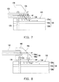
- FIG. 1 a schematic view of the optical coupling module according to an exemplary embodiment.
- FIG. 2 is the schematic side view of the optical coupling module of FIG. 1 .
- FIG. 3A is the schematic view of the optical coupling module according to another exemplary embodiment.
- FIG. 3B is the schematic side view of the optical coupling module of FIG. 3A .
- FIG. 4A is the schematic view of the optical coupling module according to another exemplary embodiment.
- FIG. 4B is the schematic side view of the optical coupling module of the FIG. 4A .
- FIG. 5A is the schematic view of the optical coupling module according to another exemplary embodiment.
- FIG. 5B is an optical simulation data diagram of the optical coupling module of FIG. 5A .
- FIG. 6A is a schematic perspective view of the optical coupling module of FIG. 5A .
- FIG. 6B is optical simulation data diagrams of the optical coupling module of FIG. 6A .
- FIG. 7 is the schematic view of the optical coupling module according to another exemplary embodiment.
- FIG. 8 is the schematic view of the optical coupling module according to another exemplary embodiment.
- FIG. 1 is a schematic view of optical coupling module according to an exemplary embodiment.
- the optical coupling module 100 may include a carrier 110 , a silicon photonic substrate 120 , and an optical waveguide module 130 .
- the carrier 110 has a carrying surface 112 for carrying the silicon photonic substrate 120 and optical waveguide module 130 successively.
- the silicon photonic substrate 120 is bonded to the carrying surface 112 of the carrier 110 and adapted to transmit the light (i.e., optical signal), wherein the silicon photonic substrate 120 has a first surface 122 and at least one first grating 124 disposed on the first surface 122 for the light which passes through the first grating 124 .
- the optical waveguide module 130 is bonded to the carrier through the silicon photonic substrate 120 and includes an optical waveguide 132 for holding the light within.
- the optical waveguide 132 may be an optical fiber which further includes a core 132 a for transmitting the light and a cladding 132 b for covering the core 132 a and confining the light within the core 132 a by total internal reflection.
- the carrier 110 and optical waveguide module 130 of the present embodiment may be formed by the glass substrates, the silicon substrates, or the ceramic substrates. However, the present embodiment is not limited herein.
- the optical waveguide 132 has an end 132 c disposed in corresponding to the first grating 124 of the silicon photonic substrate 120 .
- the optical waveguide module 130 has a reflective surface 134 coupled to the end 132 c of the optical waveguide 132 and adapted to reflect the light emerging from or incident into the first grating 124 to form an optical path between the silicon photonic substrate 120 and the optical waveguide 132 for transmitting the light.
- a reflective coating layer 138 may be disposed on the reflective surface 134 , wherein the reflective coating layer 138 may be composed of gold, silver, copper, aluminum, chromium, or the combination thereof.
- the reflective surface 134 may be set at an angle relative to a longitudinal axis A 1 of the optical waveguide 132 .
- the end 132 c of the optical waveguide 132 may be also formed as a reflective surface in compliance with the reflective surface 134 of the optical waveguide module 130 .
- the optical waveguide 132 might be physical contact with or proximately close to the first grating 124 on the first surface 122 . Therefore, through the aforementioned configuration, the coupling loss of the optical coupling module 100 can be limited to around 3 dB. Particularly, through thinning the thickness of the cladding 132 b , the coupling loss of the present optical coupling module 100 can be further lowering to below 3 dB.
- the angle of the reflective surface 134 relative to the perpendicular direction of the longitudinal axis A 1 of the optical waveguide 132 may be ranged from 30 degrees to 70 degrees.
- the aforementioned angle of the reflective surface 134 is at 32 degrees when the light emits at a wavelength of 1310 nm and at 51 degrees when the light emits at a wavelength of 1551 nm.
- the first grating 124 on the first surface 122 of the silicon photonic substrate 120 may be formed at an angle at which the light passing through may be diffracted, which causes the light to leak out in a specific direction.
- the angle of the first grating 124 relative to the normal line of the first surface 122 of the silicon photonic substrate 120 may be ranged from 10 degrees to 30 degrees.
- the optical waveguide 132 may transmit the light from a light source 180 , and the light may pass through the silicon photonic substrate 120 to the first grating 124 . The light is diffracted through the first grating 124 and coupled into the end 132 c of the optical waveguide 132 .
- the end 132 c of the optical waveguide 132 may be coated with the reflective material for destroying the total reflection of the light.
- the reflective material may be composed of, for example but not limited to, gold, silver, copper, aluminum, chromium, or the combination thereof.
- the reflectivity of the aforementioned reflective materials is above 90%, and the selectivity of the reflective material might be depending on the varying wavelengths of the light.
- the silicon photonic substrate 120 may further include a silicon waveguide 126 disposed close to the first surface 122 and corresponding to the light source 180 , wherein the grating 128 is disposed along the longitudinal direction of silicon photonic substrate 120 for transmitting the light.
- a laser source may be utilized as the light source 180 to emit the laser light.
- at least one grating 128 may be disposed at the silicon waveguide 126 and corresponding to the light source 180 for receiving and diffracting the light incident from the light source 180 .
- the silicon photonic substrate 120 may be bonded on the carrying surface 112 of the carrier 110 through flip chip bonding or wire bonding.
- the silicon photonic substrate 120 may ensure that the light source 180 is optically connected with the silicon waveguide 126 in the silicon photonic substrate 120 and the optical waveguide module 130 to transmit and receive the light (i.e., optical signal).
- a plurality of anti-reflective coating layers might be disposed on the interface between the optical waveguide 132 and the first grating 124 to protect against light leak and loss due to the reflection during the light transmission.
- the anti-reflective coating layers might be composed of, for example, a refractive index matching liquid, wherein the magnitude of the refractive index of the refractive index matching liquid is between the refractive indices of the optical waveguide 132 and the first grating 124 .
- FIG. 2 is the schematic side view of the optical coupling module of FIG. 1 .
- the optical waveguide module 130 may be bonded to the carrying surface 112 of the carrier 110 through, for example, solder bumps for aligning the relative positions of the optical waveguide module 130 and the carrier 110 , and otherwise spacing therebetween.
- the silicon photonic substrate 120 is disposed between the optical waveguide module 130 and the carrier 110 , wherein the silicon photonic substrate 120 is bonded on the carrying surface 112 of the carrier 110 and aligning with the optical waveguide 132 .
- FIG. 3 is the schematic view of the optical coupling module according to another exemplary embodiment.
- FIG. 3B is the schematic side view of the optical coupling module of 3 A.
- the silicon photonic substrate 120 further includes a second surface 123 opposite the first surface 122
- the interposer 140 further includes a third surface 142 .
- the silicon photonic substrate 120 is bonded to the interposer 140 by facing the second surface 123 to the third surface 142 of the interposer 140 through the positioning element such as the alignment pads 174 or v-grooves.
- the optical waveguide 132 might be fixed on the interposer 140 through a v-groove 148 .
- a light guiding portion 160 such as a light guiding hole, may be disposed between the first grating 124 on the first surface 122 and the second surface 123 of the silicon photonic substrate 120 for transmitting the light between the first grating 124 and the optical waveguide 132 .
- the light guiding portion 160 might be composed of at least one light guiding hole formed in the silicon photonic substrate 120 through etching, mechanical or laser drilling.
- a metal reflective layer 160 a may be deposited on the wall of the light guiding portion 160 , so as to enhance the light reflecting effects. Accordingly, as the light is diffracted from the first grating 124 and passing through the light guiding portion 160 , the light is effectively converged inside of the light guiding portion 160 without loss to the exterior, thus the effectiveness of the light transmitting is enhanced.
- FIG. 4 is the schematic view of the optical coupling module according to another exemplary embodiment.
- FIG. 4B is the schematic side view of the optical coupling module of the FIG. 4A .
- the silicon photonic substrate 120 is bonded to the interposer 140 by facing the first surface 122 to the third surface 142 of the interposer 140 through the bonding method such as flip-chip bonding or the alignment pads 174 .
- the end 132 c of the optical waveguide 132 is located over the third surface 142 and aligned with the first grating 124 , wherein the optical waveguide 132 may be fixed to the interposer 140 though the positioning elements such as v-grooves.
- a reflective surface 144 is formed on the interposer 140 and faces the end 132 c of the optical waveguide 132 .
- the reflective surface 144 of the interposer 140 of the present embodiment is set at an angle relative to the longitudinal axis A 1 of the optical waveguide 132 .
- the angle of reflective surface 144 of the interposer 140 relative to the perpendicular direction of the longitudinal axis A 1 of the optical waveguide 132 is ranged from 30 degrees to 70 degrees.
- the reflective surface 144 might be further coated with metal reflective coating layer 144 a to reflect the light diffracted from the first gratings 124 to the optical waveguide 132 for transmitting the light incident from the light source 180 .
- FIG. 5A is the schematic view of the optical coupling module according to another exemplary embodiment.
- FIG. 5B is an optical simulation data diagram of the optical coupling module corresponding to FIG. 5A .
- the optical coupling module 100 may further include a holder 135 for holding the optical waveguide 132 , wherein the holder 135 is fixed on the silicon photonic substrate 120 and the interposer 140 through the positioning elements 170 . Therefore, in the present embodiment, the alignments between the silicon photonic substrate 120 , the interposer 140 , and the optical waveguide 132 in different axis directions could be implemented through the positioning elements 170 .
- the positioning elements 170 might adjust the vertical height of the gap between the optical waveguide 132 and the silicon photonic substrate 120 in the perpendicular direction (i.e., Z-axis direction) of the first surface 122 of the silicon photonic substrate 120 .
- the silicon photonic substrate 120 might be a Silicon-on-Insulator (SOI) substrate which includes a silicon layer 120 a for transmitting the light, a silicon substrate layer 120 b and a buried oxide layer 120 c therebetween.
- SOI Silicon-on-Insulator
- the coupling loss of the optical coupling between the silicon photonic substrate 120 and the optical waveguide 132 can be limited to below 3 dB.
- FIG. 6A is a schematic perspective view of the optical coupling module of FIG. 5A .
- FIG. 6B is the optical simulation data diagrams of the optical coupling module of FIG. 6A .
- the optical waveguide 132 may be aligned with the silicon photonic substrate 120 further in the directions of X, Y, Z axes through the positioning elements 170 .
- the optical waveguide 132 might be shifted along the different axis directions relatively to the silicon photonic substrate 120 .
- the misalignment tolerance at 1 dB of the coupling loss is around 5 ⁇ m.
- the misalignment tolerance at 1 dB of the coupling loss is around 15 ⁇ m.
- the misalignment tolerance at 1 dB of the coupling loss is around 6 ⁇ m.
- FIG. 7 is the schematic view of the optical coupling module according to another exemplary embodiment.
- at least one second grating 136 may be formed at the end optical waveguide 132 and aligned corresponding to the first grating 124 on the first surface 122 of the silicon photonic substrate 120 .
- the second grating 136 is gradually changed from being perpendicular to the longitudinal axis A 1 of the optical waveguide 132 to being tilted at a specific angle ⁇ relatively to the perpendicular direction of the longitudinal axis A 1 of the optical waveguide 132 .
- the aforementioned specific tilting angle ⁇ is matched up with the light emitting angle of the first grating 124 on the first surface 122 .
- the titling angle ⁇ of the second grating 136 may be ranged from 15 degrees to 45 degrees in the present embodiment for redirecting the light at angles other than 90 degrees.
- the light passing through the optical waveguide 132 will be diffracted through the second grating 136 , then redirected and coupled into the first grating 124 of the silicon photonic substrate 120 .
- the light receiving angle of the first grating 124 relative to the normal line of the first surface 122 is ranged from 6 degrees to 12 degrees. Otherwise, in the present embodiment, the period of the first grating 124 is matching with the second grating 136 .
- FIG. 8 is the schematic view of the optical coupling module according to another exemplary embodiment.
- the optical coupling module of the FIG. 8 of the present embodiment further includes an optical packaging mechanism 190 disposed between the first grating 124 of the silicon photonic substrate 120 and the end 132 c of the optical waveguide 132 .
- the optical packaging mechanism 190 is bonded to silicon photonic substrate 120 through a plurality of the positioning elements 170 .
- the optical packaging mechanism 190 includes a reflective surface 192 , an optical waveguide holder 194 , and an external lens 196 .
- the reflective surface 192 is aligned with the reflecting paths of the light, and the holder 194 may be aligned along the longitudinal axis A 1 of the optical waveguide 132 to be paralleled to the silicon photonic substrate 120 .
- the external lens 196 is disposed corresponding to the first grating 124 of the silicon photonic substrate 120 and end 132 c of the optical waveguide 132 .
- the external lens 196 includes a first lens 196 a and a second lens 196 b respectively disposed corresponding to the end 132 c of the optical waveguide 132 and the first grating 124 of the silicon photonic substrate 120 .
- the light is incident from the optical waveguide 132 and refracted through the first lens 196 a .
- the first lens 196 a may be a collimator lens which directs the light to the reflective surface 192 . Otherwise, the reflective surface 192 may be coated with the reflective coating to destruct the total refection of the light.
- the light is reflected through the reflective surface 192 at a specific reflecting angle ranged from 30 degrees to 70 degrees, and then reflected into the second lens 196 b .
- the propagating light is coupled into the first grating 124 of the silicon photonic substrate 120 through adjusting and positioning the second lens 196 b .
- the relative position between the optical packaging mechanism 190 and silicon photonic substrate 120 is adjusted through the positioning elements 170 , so as to fulfill the requirement of alignment accuracy.
- the optical coupling module includes the silicon photonic substrate and the optical waveguide, wherein the silicon photonic substrate is optically coupled with the optical waveguide to form an optical path for the light (or optical signal) transmission.
- a reflective surface is disposed at the end of the optical waveguide and tilted relatively to the longitudinal axis of the optical waveguide with an angle at which the incident light is reflected.
- the gratings are respectively disposed at the end of the optical waveguide and on the surface of the silicon photonic substrate correspondingly to the reflective surface of the optical waveguide.
- the reflective angle of the light can be changed through aligning the gratings and the reflective surface of optical waveguide at a specific relative angle.
- the alignment tolerance and optical coupling efficiency could be enhanced through the alignment between the gratings of the silicon photonic substrate and the reflective surface of the optical waveguide.
- the size of optical coupling module and the silicon photonic substrate thereof can be further minimized.
- the manufacturing cost and time consuming on the aligning process of the optical coupling module could be greatly reduced, such that the applications of the optical coupling module will be even more prevailed.
Abstract
An optical coupling module includes a silicon photonic substrate, and an optical waveguide module. The silicon photonic substrate has a first surface and a first grating on the first surface for diffracting the light which passes through the grating. The optical waveguide module is disposed on the silicon photonic substrate, wherein the optical waveguide module includes an optical waveguide having an end disposed in corresponding to the first grating of the silicon photonic substrate. Otherwise, the optical waveguide module has a reflective surface coupled to the end of the optical waveguide and adapted to reflect the light emerging from or incident into the grating to form an optical path between the silicon photonic substrate and the optical waveguide for transmitting the light.
Description
This application claims the priority benefit of U.S. provisional application No. 61/871,319 filed on Aug. 29, 2013. The entirety of the above-mentioned patent application is hereby incorporated by reference herein and made a part of this specification.
The disclosure is related to an optical coupling module for optically coupling a silicon photonic substrate and an optical waveguide.
In recent years, as a result of storage capacity expansion, processing speed increase, and device volume reduction of optical communication systems, technology of implementing a photonic-based electronic circuit portion and optical circuit portion in one chip is gradually getting more and more attentions.
Specifically, an optical coupling device is implemented and optically coupled with an external element using a grating coupler or a side coupler formed on a silicon photonics chip. The optical coupling device is coupled between a planar optical waveguide on the silicon photonic chip and an optical fiber. The method of coupling the optical fiber and the optical waveguide on the silicon photonic chip could be generally classified into two kinds, side coupling and grating coupling. The side coupling implemented through a side coupler formed on the silicon photonics chip works independently of the wavelength. However, the side coupler has a very small optical alignment tolerance between the silicon photonic chip and the optical fiber.
On the other hand, the grating coupling is the method of directly coupling the light (or optical signal) into the optical waveguide through the gratings. The grating coupler has larger optical alignment tolerance; however, it is sensitive to the wavelength. Otherwise, in the current silicon photonic chip packaging design, through the coupling between the gratings and the optical waveguide could increase the alignment tolerance. Nevertheless, owing to the approximately perpendicular angle, about 10 degrees to 20 degrees, between the gratings and optical waveguide, there might the concerns in the difficulties of processing the optical alignments between the gratings on the silicon photonic chip and optical waveguide.
The present disclosure is directed to an optical coupling module, wherein the optical coupling module includes the grating and planar optical waveguide on the silicon photonic substrate, and another optical waveguide fixed by the interposer or holder, so as to transmit the incident light from the light source through the silicon photonic substrate to the optical waveguide, or vice versa.
One of exemplary embodiments provides an optical coupling module which includes a silicon photonic substrate, and an optical waveguide module. The silicon photonic substrate is adapted to transmit a light. The silicon photonic substrate has a first surface and a first grating on the first surface for diffracting the light which passes through the first grating. The optical waveguide module is disposed on the silicon photonic substrate, wherein the optical waveguide module includes an optical waveguide having an end disposed corresponding to the first grating of the silicon substrate. Otherwise, the optical waveguide module has a reflective surface coupled to the end of the optical waveguide and adapted to reflect the light emerging from or incident into the first grating to form an optical path between the silicon photonic substrate and the optical waveguide for transmitting the light.
Based on the aforementioned description, the optical coupling module includes the silicon photonic substrate and the optical waveguide, wherein the silicon photonic substrate is optically coupled with the optical waveguide. Otherwise, a reflective surface is disposed at the end of the optical waveguide, wherein the reflective surface is formed at angel relative to the longitudinal axis of the optical waveguide. Moreover, the magnitude of the relative angle between the reflective surface and the longitudinal axis of the optical waveguide is depending on the reflecting path of the light. Furthermore, the gratings are disposed at the ends of the silicon photonic substrate and the optical waveguide for diffracting the incident light. The reflective angle of the light can be changed through the alignments of the gratings and the optical waveguides. Therefore, the alignment tolerance and optical coupling efficiency could be enhanced through the configuration of the gratings and the reflective surface. Otherwise, owing to the silicon photonic substrate can be optically aligned with the optical waveguide through the above-mentioned configurations which has the greater alignment tolerance. Therefore, there is no need of forming the positioning alignments such as v-grooves on the limited surface area of the silicon photonic substrate. As a result, the manufacturing cost and time consuming on processing the silicon photonic substrate can be further reduced or minimized, which may enhance the productivity and manufacturing efficiency due to the simplified structure and lower processing cost.
To make the above features and advantages of the disclosure more comprehensible, several embodiments accompanied with drawings are described in detail as follows.
The accompanying drawings are included to provide further understanding, and are incorporated in and constitute a part of this specification. The drawings illustrate exemplary embodiments and, together with the description, serve to explain the principles of the disclosure.
It is to be understood that both of the foregoing and other detailed descriptions, features, and advantages are intended to be described more comprehensively by providing embodiments accompanied with Figures hereinafter. In the following embodiments, wordings used to indicate directions, such as “up,” “down,” “front,” “back,” “left,” and “right”, merely refer to directions in the accompanying drawings. Therefore, the directional wording is used to illustrate rather than limit the exemplary embodiments. The present embodiment is approximately identical to the other embodiments, and same or similar reference numerals used in the different embodiments represent the same or similar elements.
Besides, the optical waveguide 132 has an end 132 c disposed in corresponding to the first grating 124 of the silicon photonic substrate 120. The optical waveguide module 130 has a reflective surface 134 coupled to the end 132 c of the optical waveguide 132 and adapted to reflect the light emerging from or incident into the first grating 124 to form an optical path between the silicon photonic substrate 120 and the optical waveguide 132 for transmitting the light. In addition, a reflective coating layer 138 may be disposed on the reflective surface 134, wherein the reflective coating layer 138 may be composed of gold, silver, copper, aluminum, chromium, or the combination thereof. In the present embodiment, the reflective surface 134 may be set at an angle relative to a longitudinal axis A1 of the optical waveguide 132. Otherwise, the end 132 c of the optical waveguide 132 may be also formed as a reflective surface in compliance with the reflective surface 134 of the optical waveguide module 130. Furthermore, in the present embodiment, the optical waveguide 132 might be physical contact with or proximately close to the first grating 124 on the first surface 122. Therefore, through the aforementioned configuration, the coupling loss of the optical coupling module 100 can be limited to around 3 dB. Particularly, through thinning the thickness of the cladding 132 b, the coupling loss of the present optical coupling module 100 can be further lowering to below 3 dB.
Specifically, the angle of the reflective surface 134 relative to the perpendicular direction of the longitudinal axis A1 of the optical waveguide 132 may be ranged from 30 degrees to 70 degrees. In some more preferable examples, the aforementioned angle of the reflective surface 134 is at 32 degrees when the light emits at a wavelength of 1310 nm and at 51 degrees when the light emits at a wavelength of 1551 nm. In the present embodiment, the first grating 124 on the first surface 122 of the silicon photonic substrate 120 may be formed at an angle at which the light passing through may be diffracted, which causes the light to leak out in a specific direction. For example, in the present embodiment, the angle of the first grating 124 relative to the normal line of the first surface 122 of the silicon photonic substrate 120 may be ranged from 10 degrees to 30 degrees.
Referring again to FIG. 1 , the optical waveguide 132 may transmit the light from a light source 180, and the light may pass through the silicon photonic substrate 120 to the first grating 124. The light is diffracted through the first grating 124 and coupled into the end 132 c of the optical waveguide 132. In the present embodiment, the end 132 c of the optical waveguide 132 may be coated with the reflective material for destroying the total reflection of the light. The reflective material may be composed of, for example but not limited to, gold, silver, copper, aluminum, chromium, or the combination thereof. The reflectivity of the aforementioned reflective materials is above 90%, and the selectivity of the reflective material might be depending on the varying wavelengths of the light.
On the other hand, the silicon photonic substrate 120 may further include a silicon waveguide 126 disposed close to the first surface 122 and corresponding to the light source 180, wherein the grating 128 is disposed along the longitudinal direction of silicon photonic substrate 120 for transmitting the light. In the present embodiment, a laser source may be utilized as the light source 180 to emit the laser light. Besides, at least one grating 128 may be disposed at the silicon waveguide 126 and corresponding to the light source 180 for receiving and diffracting the light incident from the light source 180. Furthermore, the silicon photonic substrate 120 may be bonded on the carrying surface 112 of the carrier 110 through flip chip bonding or wire bonding. Accordingly, through the configuration of the silicon photonic substrate 120, optical waveguide 132, and the carrier 110, the silicon photonic substrate 120 may ensure that the light source 180 is optically connected with the silicon waveguide 126 in the silicon photonic substrate 120 and the optical waveguide module 130 to transmit and receive the light (i.e., optical signal).
Furthermore, in the present embodiment, a plurality of anti-reflective coating layers (not illustrated) might be disposed on the interface between the optical waveguide 132 and the first grating 124 to protect against light leak and loss due to the reflection during the light transmission. The anti-reflective coating layers might be composed of, for example, a refractive index matching liquid, wherein the magnitude of the refractive index of the refractive index matching liquid is between the refractive indices of the optical waveguide 132 and the first grating 124.
In the present embodiment, the external lens 196 includes a first lens 196 a and a second lens 196 b respectively disposed corresponding to the end 132 c of the optical waveguide 132 and the first grating 124 of the silicon photonic substrate 120. The light is incident from the optical waveguide 132 and refracted through the first lens 196 a. The first lens 196 a may be a collimator lens which directs the light to the reflective surface 192. Otherwise, the reflective surface 192 may be coated with the reflective coating to destruct the total refection of the light. On the other hand, the light is reflected through the reflective surface 192 at a specific reflecting angle ranged from 30 degrees to 70 degrees, and then reflected into the second lens 196 b. The propagating light is coupled into the first grating 124 of the silicon photonic substrate 120 through adjusting and positioning the second lens 196 b. In the present embodiment, the relative position between the optical packaging mechanism 190 and silicon photonic substrate 120 is adjusted through the positioning elements 170, so as to fulfill the requirement of alignment accuracy.
In summary, the optical coupling module includes the silicon photonic substrate and the optical waveguide, wherein the silicon photonic substrate is optically coupled with the optical waveguide to form an optical path for the light (or optical signal) transmission. Otherwise, a reflective surface is disposed at the end of the optical waveguide and tilted relatively to the longitudinal axis of the optical waveguide with an angle at which the incident light is reflected. Moreover, the gratings are respectively disposed at the end of the optical waveguide and on the surface of the silicon photonic substrate correspondingly to the reflective surface of the optical waveguide. Furthermore, the reflective angle of the light can be changed through aligning the gratings and the reflective surface of optical waveguide at a specific relative angle. Therefore, the alignment tolerance and optical coupling efficiency could be enhanced through the alignment between the gratings of the silicon photonic substrate and the reflective surface of the optical waveguide. Thus, the size of optical coupling module and the silicon photonic substrate thereof can be further minimized. Otherwise, with the above-mentioned configuration, there is no need of forming positioning elements such as the v-grooves on the limited surface area of the silicon photonic substrate for aligning. As a result, the manufacturing cost and time consuming on the aligning process of the optical coupling module could be greatly reduced, such that the applications of the optical coupling module will be even more prevailed.
Although the disclosure has been described with reference to the above embodiments, it will be apparent to one of ordinary skill in the art that modifications to the described embodiments may be made without departing from the spirit of the disclosure. Accordingly, the scope of the disclosure will be defined by the attached claims and not by the above detailed descriptions.
Claims (6)
1. An optical coupling module, comprising:
a silicon photonic substrate adapted to transmit a light, wherein the silicon photonic substrate has a first surface and a second surface opposite to the first surface, a first grating disposed in the first surface for diffracting the light which passes through the first grating;
an optical waveguide module disposed on the second surface of the silicon photonic substrate, wherein the optical waveguide module comprises an optical waveguide having an end disposed in corresponding to the first grating of the silicon photonic substrate; and
an interposer, wherein the silicon photonic substrate is bonded to the interposer by facing the second surface to the interposer and a light guiding portion is disposed between the first grating and the second surface and penetrates through the silicon photonic substrate for transmitting the light between the first grating and the end of the optical waveguide.
2. The optical coupling module as claimed in claim 1 , wherein the optical waveguide module is fixed to the interposer.
3. The optical coupling module as claimed in claim 1 , wherein the reflective surface is formed on the interposer and faces the end of the optical waveguide.
4. The optical coupling module as claimed in claim 1 , wherein the reflective surface is set at an angle relative to a longitudinal axis of the optical waveguide, and the angle is ranged from 30 degrees to 70 degrees.
5. The optical coupling module as claimed in claim 1 , wherein the optical waveguide is a fiber.
6. An optical coupling module, comprising:
a silicon photonic substrate adapted to transmit a light, wherein the silicon photonic substrate has a first surface and a second surface opposite to the first surface, a first grating disposed on the first surface for diffracting the light which passes through the first grating;
an optical waveguide module disposed on the silicon photonic substrate, wherein the optical waveguide module comprises an optical waveguide having an end disposed in corresponding to the first grating of the silicon photonic substrate, and the optical waveguide module has a reflective surface coupled to the end of the optical waveguide and adapted to reflect the light emerging from or incident into the first grating, to form an optical path between the silicon photonic substrate and the optical waveguide for transmitting the light; and
an interposer, wherein the silicon photonic substrate is bonded to the interposer by facing the second surface to the interposer and a light guiding portion is disposed between the first grating and the second surface for transmitting the light between the first grating and the end of the optical waveguide, the light guiding portion is composed of at least one light guiding hole, and at least one metal reflective layer is on the wall of the light guiding hole.
Priority Applications (1)
| Application Number | Priority Date | Filing Date | Title |
|---|---|---|---|
| US14/472,390 US9613886B2 (en) | 2013-08-29 | 2014-08-29 | Optical coupling module |
Applications Claiming Priority (2)
| Application Number | Priority Date | Filing Date | Title |
|---|---|---|---|
| US201361871319P | 2013-08-29 | 2013-08-29 | |
| US14/472,390 US9613886B2 (en) | 2013-08-29 | 2014-08-29 | Optical coupling module |
Publications (2)
| Publication Number | Publication Date |
|---|---|
| US20150063745A1 US20150063745A1 (en) | 2015-03-05 |
| US9613886B2 true US9613886B2 (en) | 2017-04-04 |
Family
ID=52582049
Family Applications (4)
| Application Number | Title | Priority Date | Filing Date |
|---|---|---|---|
| US14/472,390 Active 2034-10-03 US9613886B2 (en) | 2013-08-29 | 2014-08-29 | Optical coupling module |
| US14/472,391 Active US9252079B2 (en) | 2013-08-29 | 2014-08-29 | Substrate, method of fabricating the same, and application the same |
| US14/472,400 Active US9171779B2 (en) | 2013-08-29 | 2014-08-29 | Semiconductor laser structure |
| US14/864,810 Active US9653382B2 (en) | 2013-08-29 | 2015-09-24 | Semiconductor laser structure |
Family Applications After (3)
| Application Number | Title | Priority Date | Filing Date |
|---|---|---|---|
| US14/472,391 Active US9252079B2 (en) | 2013-08-29 | 2014-08-29 | Substrate, method of fabricating the same, and application the same |
| US14/472,400 Active US9171779B2 (en) | 2013-08-29 | 2014-08-29 | Semiconductor laser structure |
| US14/864,810 Active US9653382B2 (en) | 2013-08-29 | 2015-09-24 | Semiconductor laser structure |
Country Status (3)
| Country | Link |
|---|---|
| US (4) | US9613886B2 (en) |
| CN (1) | CN104425394B (en) |
| TW (2) | TWI552234B (en) |
Cited By (12)
| Publication number | Priority date | Publication date | Assignee | Title |
|---|---|---|---|---|
| US20160266322A1 (en) * | 2015-03-12 | 2016-09-15 | Samtec, Inc. | Optical module including silicon photonics chip and coupler chip |
| US20190079243A1 (en) * | 2017-09-14 | 2019-03-14 | Lightwave Logic Inc. | Guide transition device and method |
| US10317632B2 (en) * | 2016-12-06 | 2019-06-11 | Finisar Corporation | Surface coupled laser and laser optical interposer |
| US10656333B2 (en) | 2014-11-11 | 2020-05-19 | Ii-Vi Delaware Inc. | Two-stage adiabatically coupled photonic systems |
| US10809456B2 (en) | 2018-04-04 | 2020-10-20 | Ii-Vi Delaware Inc. | Adiabatically coupled photonic systems with fan-out interposer |
| US10826267B2 (en) | 2015-12-17 | 2020-11-03 | Ii-Vi Delaware Inc. | Surface coupled systems |
| US10935868B2 (en) * | 2017-09-28 | 2021-03-02 | The Charles Stark Draper Laboratory, Inc. | System and method for diffractive steering of electromagnetic radiation |
| US10992104B2 (en) | 2015-12-17 | 2021-04-27 | Ii-Vi Delaware, Inc. | Dual layer grating coupler |
| US11243450B2 (en) * | 2017-01-30 | 2022-02-08 | The Charles Stark Draper Laboratory, Inc. | Saw modulator having optical power component for extended angular redirection of light |
| US11404850B2 (en) | 2019-04-22 | 2022-08-02 | Ii-Vi Delaware, Inc. | Dual grating-coupled lasers |
| US11435522B2 (en) | 2018-09-12 | 2022-09-06 | Ii-Vi Delaware, Inc. | Grating coupled laser for Si photonics |
| US11693169B2 (en) | 2021-03-08 | 2023-07-04 | Mellanox Technologies, Ltd. | Silicon photonics collimator for wafer level assembly |
Families Citing this family (33)
| Publication number | Priority date | Publication date | Assignee | Title |
|---|---|---|---|---|
| US9360620B2 (en) * | 2012-08-29 | 2016-06-07 | Aurrion, Inc. | Thermal management for photonic integrated circuits |
| US9159861B2 (en) * | 2013-10-21 | 2015-10-13 | Oracle International Corporation | Method for singulating hybrid integrated photonic chips |
| JP2015184375A (en) * | 2014-03-20 | 2015-10-22 | 株式会社東芝 | Optical wiring device and manufacturing method thereof |
| DE102014105188A1 (en) * | 2014-04-11 | 2015-10-15 | Osram Opto Semiconductors Gmbh | Semiconductor chip, optoelectronic component with semiconductor chip and method for producing a semiconductor chip |
| EP3213133B1 (en) | 2014-10-27 | 2019-12-25 | Elenion Technologies, LLC | Photonic interface for electronic circuit |
| US9318376B1 (en) * | 2014-12-15 | 2016-04-19 | Freescale Semiconductor, Inc. | Through substrate via with diffused conductive component |
| US9482818B2 (en) * | 2015-02-23 | 2016-11-01 | Cisco Technology, Inc. | Optically coupling waveguides |
| TWM536364U (en) * | 2015-03-12 | 2017-02-01 | 山姆科技公司 | Optical module including silicon photonics chip and coupler chip |
| WO2016146963A1 (en) * | 2015-03-16 | 2016-09-22 | Popovich, Milan, Momcilo | Waveguide device incorporating a light pipe |
| US9786641B2 (en) | 2015-08-13 | 2017-10-10 | International Business Machines Corporation | Packaging optoelectronic components and CMOS circuitry using silicon-on-insulator substrates for photonics applications |
| US9853446B2 (en) | 2015-08-27 | 2017-12-26 | Qualcomm Incorporated | Integrated circuit (IC) package comprising electrostatic discharge (ESD) protection |
| US9793682B2 (en) * | 2015-11-18 | 2017-10-17 | International Business Machines Corporation | Silicon photonic chip with integrated electro-optical component and lens element |
| US10861763B2 (en) | 2016-11-26 | 2020-12-08 | Texas Instruments Incorporated | Thermal routing trench by additive processing |
| US10529641B2 (en) | 2016-11-26 | 2020-01-07 | Texas Instruments Incorporated | Integrated circuit nanoparticle thermal routing structure over interconnect region |
| US11004680B2 (en) | 2016-11-26 | 2021-05-11 | Texas Instruments Incorporated | Semiconductor device package thermal conduit |
| US10256188B2 (en) | 2016-11-26 | 2019-04-09 | Texas Instruments Incorporated | Interconnect via with grown graphitic material |
| US10811334B2 (en) | 2016-11-26 | 2020-10-20 | Texas Instruments Incorporated | Integrated circuit nanoparticle thermal routing structure in interconnect region |
| US11676880B2 (en) | 2016-11-26 | 2023-06-13 | Texas Instruments Incorporated | High thermal conductivity vias by additive processing |
| TWI633906B (en) * | 2017-01-12 | 2018-09-01 | 財團法人工業技術研究院 | Light source module, phototherapy apparatus and method of using the same |
| JP2018142592A (en) * | 2017-02-27 | 2018-09-13 | パナソニックIpマネジメント株式会社 | Light source module, illumination device, and mobile body |
| US10511146B2 (en) * | 2017-11-14 | 2019-12-17 | Lightwave Logic Inc. | Guide transition device with digital grating deflectors and method |
| KR20190088803A (en) | 2018-01-19 | 2019-07-29 | 삼성전자주식회사 | Semiconductor laser device and method of manufacturing the same |
| CN108682661A (en) * | 2018-04-17 | 2018-10-19 | 中芯集成电路(宁波)有限公司 | A kind of forming method of SOI substrate and SOI substrate |
| US10509167B2 (en) * | 2018-04-23 | 2019-12-17 | Hewlett Packard Enterprise Development Lp | Optical phase difference calculation using analog processing |
| CN108878349A (en) * | 2018-06-27 | 2018-11-23 | 北京工业大学 | A kind of structure and preparation method thereof of novel SOI substrate |
| US11002915B2 (en) * | 2018-06-29 | 2021-05-11 | Taiwan Semiconductor Manufacturing Co., Ltd. | Fiber-to-chip grating coupler for photonic circuits |
| CN111162067A (en) * | 2018-11-08 | 2020-05-15 | 喆富创新科技股份有限公司 | Optical coupling structure for forming laminated pattern on wafer |
| US10651110B1 (en) * | 2018-12-31 | 2020-05-12 | Juniper Networks, Inc. | Efficient heat-sinking in PIN diode |
| US10895702B2 (en) * | 2019-04-01 | 2021-01-19 | Google Llc | Integrated heater structures in a photonic integrated circuit for solder attachment applications |
| JP7147979B2 (en) * | 2019-06-10 | 2022-10-05 | 日本電信電話株式会社 | optical device |
| US11435528B1 (en) * | 2019-11-06 | 2022-09-06 | Meta Platforms Technologies, Llc | Photonic integrated circuits with integrated optical conditioning elements |
| EP4044221A1 (en) * | 2021-02-10 | 2022-08-17 | AT & S Austria Technologie & Systemtechnik Aktiengesellschaft | Heat removal architecture for stack-type component carrier with embedded component |
| US20240069291A1 (en) * | 2022-08-26 | 2024-02-29 | Taiwan Semiconductor Manufacturing Company, Ltd. | Package structure having grating coupler and manufacturing method thereof |
Citations (41)
| Publication number | Priority date | Publication date | Assignee | Title |
|---|---|---|---|---|
| US5208882A (en) * | 1991-11-14 | 1993-05-04 | Eastman Kodak Company | Hybrid thin film optical waveguide structure having a grating coupler and a tapered waveguide film |
| US5568574A (en) * | 1995-06-12 | 1996-10-22 | University Of Southern California | Modulator-based photonic chip-to-chip interconnections for dense three-dimensional multichip module integration |
| US6624444B1 (en) * | 2002-03-28 | 2003-09-23 | Intel Corporation | Electrical-optical package with capacitor DC shunts and associated methods |
| US20030185484A1 (en) * | 2002-03-28 | 2003-10-02 | Intel Corporation | Integrated optoelectrical circuit package with optical waveguide interconnects |
| US6722792B2 (en) * | 2001-01-19 | 2004-04-20 | Primarion, Inc. | Optical interconnect with integral reflective surface and lens, system including the interconnect and method of forming the same |
| US20040086011A1 (en) * | 2002-10-30 | 2004-05-06 | Photodigm, Inc. | Planar and wafer level packaging of semiconductor lasers and photo detectors for transmitter optical sub-assemblies |
| US20040101020A1 (en) * | 2002-11-26 | 2004-05-27 | Photodigm, Inc. | Packaging and passive alignment of light source to single mode fiber using microlens and precision ferrule |
| US20040105476A1 (en) * | 2002-08-19 | 2004-06-03 | Wasserbauer John G. | Planar waveguide surface emitting laser and photonic integrated circuit |
| US6789959B1 (en) | 2003-02-27 | 2004-09-14 | Xilinx, Inc. | Fiber optic integrated circuit package using micromirrors |
| US20040240788A1 (en) * | 2002-10-25 | 2004-12-02 | Jun-Fei Zheng | Optical grating coupler |
| US20050069013A1 (en) * | 2003-09-29 | 2005-03-31 | Photodigm, Inc. | Method and apparatus for wavelength division multiplexing |
| US20050141808A1 (en) * | 2003-12-24 | 2005-06-30 | National Research Council Of Canada | Optical off-chip interconnects in multichannel planar waveguide devices |
| US6952504B2 (en) * | 2001-12-21 | 2005-10-04 | Neophotonics Corporation | Three dimensional engineering of planar optical structures |
| US6975812B1 (en) * | 2000-02-09 | 2005-12-13 | Sumitomo Electric Industries, Ltd. | Optical communication device |
| US20060067617A1 (en) * | 2004-08-31 | 2006-03-30 | Gaylord Thomas K | Optical interconnects in microelectronics based on azimuthally asymmetric long-period fiber grating couplers |
| US7058261B2 (en) * | 2003-09-04 | 2006-06-06 | Sioptical, Inc. | Interfacing multiple wavelength sources to thin optical waveguides utilizing evanescent coupling |
| US20060239605A1 (en) * | 2005-02-16 | 2006-10-26 | Applied Materials, Inc. | Optical coupling to IC chip |
| US7162124B1 (en) * | 2003-03-14 | 2007-01-09 | Luxtera, Inc. | Fiber to chip coupler |
| US7190859B2 (en) * | 2000-03-16 | 2007-03-13 | Lightsmyth Technologies Inc | Distributed optical structures in a planar waveguide coupling in-plane and out-of-plane optical signals |
| US7221825B2 (en) * | 2002-12-23 | 2007-05-22 | The University Of Surrey | Optical coupler |
| US7277611B1 (en) * | 2006-08-30 | 2007-10-02 | Fujitsu, Limited | Optical interconnect platform including Bragg diffractive gratings in a bulk material |
| US20090003762A1 (en) * | 2007-06-28 | 2009-01-01 | International Business Machines Corporation | Chip to chip optical interconnect |
| US7660500B2 (en) * | 2007-05-22 | 2010-02-09 | Epicrystals Oy | Light emitting array |
| TW201028748A (en) | 2008-12-17 | 2010-08-01 | Nat Semiconductor Corp | Wafer level optoelectronic package with fiber side insertion |
| US20110069925A1 (en) * | 2009-09-24 | 2011-03-24 | Sun Microsystems, Inc. | Macro-chip including a surface-normal device |
| US20110158278A1 (en) * | 2009-12-30 | 2011-06-30 | Koch Brian R | Hybrid silicon vertical cavity laser with in-plane coupling |
| JP2011133536A (en) * | 2009-12-22 | 2011-07-07 | Nec Corp | Optical coupler |
| US20120301149A1 (en) * | 2009-09-04 | 2012-11-29 | Thierry Pinguet | Method And System For Hybrid Integration Of Optical Communication Systems |
| US20130182994A1 (en) * | 2012-01-12 | 2013-07-18 | Tyco Electronics Corporation | Optical interposer with ninety degree light bending |
| US20130202246A1 (en) * | 2012-02-03 | 2013-08-08 | Roy Meade | Active alignment of optical fiber to chip using liquid crystals |
| US20130230280A1 (en) * | 2012-03-02 | 2013-09-05 | Tyco Electronics Corporation | Modularized interposer |
| US20130279844A1 (en) * | 2011-12-15 | 2013-10-24 | Yun-Chung Na | Efficient backside-emitting/collecting grating coupler |
| US8639073B2 (en) * | 2011-07-19 | 2014-01-28 | Teraxion Inc. | Fiber coupling technique on a waveguide |
| US20140029894A1 (en) * | 2012-07-26 | 2014-01-30 | Tyco Electronics Corporation | Optical assembly with diffractive optical element |
| US20140294342A1 (en) * | 2013-03-28 | 2014-10-02 | International Business Machines Corporation | Optoelectronic packaging assembly |
| US8998509B2 (en) * | 2013-03-14 | 2015-04-07 | Oracle International Corporation | Stackable photonic interconnect module |
| EP2860560A1 (en) * | 2013-10-14 | 2015-04-15 | ams AG | Semiconductor device with optical and electrical vias |
| US20150205062A1 (en) * | 2012-12-19 | 2015-07-23 | Huawei Technologies Co., Ltd. | Optical Interposer |
| US9091827B2 (en) * | 2012-07-09 | 2015-07-28 | Luxtera, Inc. | Method and system for grating couplers incorporating perturbed waveguides |
| US9274275B2 (en) * | 2013-07-03 | 2016-03-01 | Cisco Technology, Inc. | Photonic integration platform |
| US9323014B2 (en) * | 2012-05-28 | 2016-04-26 | Mellanox Technologies Ltd. | High-speed optical module with flexible printed circuit board |
Family Cites Families (29)
| Publication number | Priority date | Publication date | Assignee | Title |
|---|---|---|---|---|
| US5226052A (en) * | 1990-05-08 | 1993-07-06 | Rohm, Ltd. | Laser diode system for cutting off the environment from the laser diode |
| US5313094A (en) | 1992-01-28 | 1994-05-17 | International Business Machines Corportion | Thermal dissipation of integrated circuits using diamond paths |
| US6054716A (en) | 1997-01-10 | 2000-04-25 | Rohm Co., Ltd. | Semiconductor light emitting device having a protecting device |
| JP4296644B2 (en) | 1999-01-29 | 2009-07-15 | 豊田合成株式会社 | Light emitting diode |
| US6288426B1 (en) | 2000-02-28 | 2001-09-11 | International Business Machines Corp. | Thermal conductivity enhanced semiconductor structures and fabrication processes |
| US6956250B2 (en) | 2001-02-23 | 2005-10-18 | Nitronex Corporation | Gallium nitride materials including thermally conductive regions |
| JP4055405B2 (en) * | 2001-12-03 | 2008-03-05 | ソニー株式会社 | Electronic component and manufacturing method thereof |
| JP4634047B2 (en) * | 2004-01-23 | 2011-02-16 | パイオニア株式会社 | Integrated semiconductor light emitting device and method for manufacturing the same |
| TWI260795B (en) | 2004-03-22 | 2006-08-21 | South Epitaxy Corp | Flip chip type- light emitting diode package |
| US7839908B2 (en) * | 2005-03-30 | 2010-11-23 | Mitsubishi Electric Corporation | Mode control waveguide laser device |
| JP4850174B2 (en) | 2005-05-23 | 2012-01-11 | 富士通セミコンダクター株式会社 | Semiconductor device and manufacturing method thereof |
| US8110823B2 (en) * | 2006-01-20 | 2012-02-07 | The Regents Of The University Of California | III-V photonic integration on silicon |
| KR101314713B1 (en) | 2006-06-16 | 2013-10-07 | 신꼬오덴기 고교 가부시키가이샤 | Semiconductor device and method of manufacturing semiconductor device, and substrate |
| JP4961617B2 (en) * | 2007-10-01 | 2012-06-27 | 新光電気工業株式会社 | WIRING BOARD, MANUFACTURING METHOD THEREOF, AND SEMICONDUCTOR DEVICE |
| TWM334549U (en) | 2007-10-30 | 2008-06-11 | Tyntek Corp | High efficiency laser diode |
| KR100896282B1 (en) | 2007-11-01 | 2009-05-08 | 엘지전자 주식회사 | LED package and method of manufacturing the same |
| TWI358180B (en) | 2007-12-25 | 2012-02-11 | Heat sink array device of high power laser diode | |
| US7639719B2 (en) | 2007-12-31 | 2009-12-29 | Intel Corporation | Thermal shunt for active devices on silicon-on-insulator wafers |
| US8310043B2 (en) | 2008-03-25 | 2012-11-13 | Bridge Semiconductor Corporation | Semiconductor chip assembly with post/base heat spreader with ESD protection layer |
| WO2009136913A1 (en) * | 2008-05-06 | 2009-11-12 | Hewlett-Packard Development Company, L.P. | System and method for a micro ring laser |
| JP5386916B2 (en) | 2008-09-30 | 2014-01-15 | ソニー株式会社 | Transistor-type protection device, semiconductor integrated circuit, and manufacturing method thereof |
| CN101741007B (en) * | 2008-11-04 | 2011-07-27 | 北京大学 | Method for preparing metallic bonding silicon substrate laser |
| DE102008063416B4 (en) | 2008-12-31 | 2014-12-31 | Globalfoundries Dresden Module One Limited Liability Company & Co. Kg | Heat dissipation in temperature-critical component areas of semiconductor devices by heat conduction, which are connected to the substrate back |
| US7883910B2 (en) | 2009-02-03 | 2011-02-08 | Industrial Technology Research Institute | Light emitting diode structure, LED packaging structure using the same and method of forming the same |
| JP2011199261A (en) * | 2010-02-24 | 2011-10-06 | Panasonic Corp | Electronic component |
| US8749018B2 (en) | 2010-06-21 | 2014-06-10 | Infineon Technologies Ag | Integrated semiconductor device having an insulating structure and a manufacturing method |
| US8476676B2 (en) | 2011-01-20 | 2013-07-02 | Alpha And Omega Semiconductor Incorporated | Trench poly ESD formation for trench MOS and SGT |
| TWI430432B (en) | 2011-01-27 | 2014-03-11 | Sinopower Semiconductor Inc | Power semiconductor device with electrostatic discharge structure and manufacturing method |
| JP2012175067A (en) * | 2011-02-24 | 2012-09-10 | Sony Corp | Image pickup device, and manufacturing method therefor, and electronic apparatus |
-
2014
- 2014-08-29 US US14/472,390 patent/US9613886B2/en active Active
- 2014-08-29 TW TW103129906A patent/TWI552234B/en active
- 2014-08-29 US US14/472,391 patent/US9252079B2/en active Active
- 2014-08-29 CN CN201410436888.3A patent/CN104425394B/en active Active
- 2014-08-29 US US14/472,400 patent/US9171779B2/en active Active
- 2014-08-29 TW TW103129810A patent/TWI589326B/en active
-
2015
- 2015-09-24 US US14/864,810 patent/US9653382B2/en active Active
Patent Citations (50)
| Publication number | Priority date | Publication date | Assignee | Title |
|---|---|---|---|---|
| US5208882A (en) * | 1991-11-14 | 1993-05-04 | Eastman Kodak Company | Hybrid thin film optical waveguide structure having a grating coupler and a tapered waveguide film |
| US5568574A (en) * | 1995-06-12 | 1996-10-22 | University Of Southern California | Modulator-based photonic chip-to-chip interconnections for dense three-dimensional multichip module integration |
| US6975812B1 (en) * | 2000-02-09 | 2005-12-13 | Sumitomo Electric Industries, Ltd. | Optical communication device |
| US7190859B2 (en) * | 2000-03-16 | 2007-03-13 | Lightsmyth Technologies Inc | Distributed optical structures in a planar waveguide coupling in-plane and out-of-plane optical signals |
| US6722792B2 (en) * | 2001-01-19 | 2004-04-20 | Primarion, Inc. | Optical interconnect with integral reflective surface and lens, system including the interconnect and method of forming the same |
| US6952504B2 (en) * | 2001-12-21 | 2005-10-04 | Neophotonics Corporation | Three dimensional engineering of planar optical structures |
| US6841842B2 (en) * | 2002-03-28 | 2005-01-11 | Intel Corporation | Method and apparatus for electrical-optical packaging with capacitive DC shunts |
| US20040036134A1 (en) * | 2002-03-28 | 2004-02-26 | Yuan-Liang Li | Method and apparatus for electrical-optical packaging with capacitive DC shunts |
| US6624444B1 (en) * | 2002-03-28 | 2003-09-23 | Intel Corporation | Electrical-optical package with capacitor DC shunts and associated methods |
| US20030183893A1 (en) * | 2002-03-28 | 2003-10-02 | Intel Corporation | Electrical-optical package with capacitor dc shunts and associated methods |
| US20030185484A1 (en) * | 2002-03-28 | 2003-10-02 | Intel Corporation | Integrated optoelectrical circuit package with optical waveguide interconnects |
| US20040105476A1 (en) * | 2002-08-19 | 2004-06-03 | Wasserbauer John G. | Planar waveguide surface emitting laser and photonic integrated circuit |
| US20040240788A1 (en) * | 2002-10-25 | 2004-12-02 | Jun-Fei Zheng | Optical grating coupler |
| US20040086011A1 (en) * | 2002-10-30 | 2004-05-06 | Photodigm, Inc. | Planar and wafer level packaging of semiconductor lasers and photo detectors for transmitter optical sub-assemblies |
| US20040101020A1 (en) * | 2002-11-26 | 2004-05-27 | Photodigm, Inc. | Packaging and passive alignment of light source to single mode fiber using microlens and precision ferrule |
| US7221825B2 (en) * | 2002-12-23 | 2007-05-22 | The University Of Surrey | Optical coupler |
| US6789959B1 (en) | 2003-02-27 | 2004-09-14 | Xilinx, Inc. | Fiber optic integrated circuit package using micromirrors |
| US7162124B1 (en) * | 2003-03-14 | 2007-01-09 | Luxtera, Inc. | Fiber to chip coupler |
| US7058261B2 (en) * | 2003-09-04 | 2006-06-06 | Sioptical, Inc. | Interfacing multiple wavelength sources to thin optical waveguides utilizing evanescent coupling |
| US20050069013A1 (en) * | 2003-09-29 | 2005-03-31 | Photodigm, Inc. | Method and apparatus for wavelength division multiplexing |
| US20050141808A1 (en) * | 2003-12-24 | 2005-06-30 | National Research Council Of Canada | Optical off-chip interconnects in multichannel planar waveguide devices |
| US20060067617A1 (en) * | 2004-08-31 | 2006-03-30 | Gaylord Thomas K | Optical interconnects in microelectronics based on azimuthally asymmetric long-period fiber grating couplers |
| US20060239605A1 (en) * | 2005-02-16 | 2006-10-26 | Applied Materials, Inc. | Optical coupling to IC chip |
| US7277611B1 (en) * | 2006-08-30 | 2007-10-02 | Fujitsu, Limited | Optical interconnect platform including Bragg diffractive gratings in a bulk material |
| US7660500B2 (en) * | 2007-05-22 | 2010-02-09 | Epicrystals Oy | Light emitting array |
| US20090003762A1 (en) * | 2007-06-28 | 2009-01-01 | International Business Machines Corporation | Chip to chip optical interconnect |
| US7480429B1 (en) * | 2007-06-28 | 2009-01-20 | International Business Machines Corporation | Chip to Chip optical interconnect |
| TW201028748A (en) | 2008-12-17 | 2010-08-01 | Nat Semiconductor Corp | Wafer level optoelectronic package with fiber side insertion |
| US20120301149A1 (en) * | 2009-09-04 | 2012-11-29 | Thierry Pinguet | Method And System For Hybrid Integration Of Optical Communication Systems |
| US20110069925A1 (en) * | 2009-09-24 | 2011-03-24 | Sun Microsystems, Inc. | Macro-chip including a surface-normal device |
| JP2011133536A (en) * | 2009-12-22 | 2011-07-07 | Nec Corp | Optical coupler |
| US8604577B2 (en) * | 2009-12-30 | 2013-12-10 | Intel Corporation | Hybrid silicon vertical cavity laser with in-plane coupling |
| US20130208752A1 (en) * | 2009-12-30 | 2013-08-15 | Brian R. Koch | Hybrid silicon vertical cavity laser with in-plane coupling |
| US8257990B2 (en) * | 2009-12-30 | 2012-09-04 | Intel Corporation | Hybrid silicon vertical cavity laser with in-plane coupling |
| US20110158278A1 (en) * | 2009-12-30 | 2011-06-30 | Koch Brian R | Hybrid silicon vertical cavity laser with in-plane coupling |
| US8639073B2 (en) * | 2011-07-19 | 2014-01-28 | Teraxion Inc. | Fiber coupling technique on a waveguide |
| US9028157B2 (en) * | 2011-12-15 | 2015-05-12 | Intel Corporation | Efficient backside-emitting/collecting grating coupler |
| US20130279844A1 (en) * | 2011-12-15 | 2013-10-24 | Yun-Chung Na | Efficient backside-emitting/collecting grating coupler |
| US20130182994A1 (en) * | 2012-01-12 | 2013-07-18 | Tyco Electronics Corporation | Optical interposer with ninety degree light bending |
| US20130202246A1 (en) * | 2012-02-03 | 2013-08-08 | Roy Meade | Active alignment of optical fiber to chip using liquid crystals |
| US20130230280A1 (en) * | 2012-03-02 | 2013-09-05 | Tyco Electronics Corporation | Modularized interposer |
| US9323014B2 (en) * | 2012-05-28 | 2016-04-26 | Mellanox Technologies Ltd. | High-speed optical module with flexible printed circuit board |
| US9091827B2 (en) * | 2012-07-09 | 2015-07-28 | Luxtera, Inc. | Method and system for grating couplers incorporating perturbed waveguides |
| US20140029894A1 (en) * | 2012-07-26 | 2014-01-30 | Tyco Electronics Corporation | Optical assembly with diffractive optical element |
| US9201200B2 (en) * | 2012-07-26 | 2015-12-01 | Tyco Electronics Corporation | Optical assembly with diffractive optical element |
| US20150205062A1 (en) * | 2012-12-19 | 2015-07-23 | Huawei Technologies Co., Ltd. | Optical Interposer |
| US8998509B2 (en) * | 2013-03-14 | 2015-04-07 | Oracle International Corporation | Stackable photonic interconnect module |
| US20140294342A1 (en) * | 2013-03-28 | 2014-10-02 | International Business Machines Corporation | Optoelectronic packaging assembly |
| US9274275B2 (en) * | 2013-07-03 | 2016-03-01 | Cisco Technology, Inc. | Photonic integration platform |
| EP2860560A1 (en) * | 2013-10-14 | 2015-04-15 | ams AG | Semiconductor device with optical and electrical vias |
Non-Patent Citations (6)
| Title |
|---|
| D.A. Louderback, et al., "VCSELs with monolithic coupling to internal horizontal waveguides using integrated diffraction gratings," Electronics Letters, Aug. 19, 2004, vol. 40, No. 17, pp. 1064-pp. 1065. |
| Dirk Taillaert, et al., "A Compact Two-dimensional Grating Coupler used as a Polarization Splitter," Photonics Technology Letters, IEEE, Sep. 2003, vol. 15, Issue: 9, pp. 1249-pp. 1251. |
| Dirk Taillaert, et al., "Compact efficient broadband grating coupler for silicon-on-insulator waveguides," Optics Letters, Dec. 1, 2004, vol. 29, No. 23, pp. 2749-pp. 2751. |
| Jelena Vuckovic, et al., "Design of photonic crystal microcavities for cavity QED," Physical Review E, Dec. 21, 2001, vol. 65, pp. 016608-1-pp. 016608-11. |
| Keith A. Bates, et al., "Gaussian beams from variable groove depth grating couplers in planar waveguides," Applied Optics, Apr. 20, 1993, vol. 32, No. 12, pp. 2112-pp. 2116. |
| Shigeki Miyanag, et al., "Intensity profile of outgoing beams from uniform and linearly tapered grating couplers," Applied Optics, Feb. 15, 1981, vol. 20, No. 4, pp. 688-pp. 695. |
Cited By (17)
| Publication number | Priority date | Publication date | Assignee | Title |
|---|---|---|---|---|
| US10656333B2 (en) | 2014-11-11 | 2020-05-19 | Ii-Vi Delaware Inc. | Two-stage adiabatically coupled photonic systems |
| US20160266322A1 (en) * | 2015-03-12 | 2016-09-15 | Samtec, Inc. | Optical module including silicon photonics chip and coupler chip |
| US10826267B2 (en) | 2015-12-17 | 2020-11-03 | Ii-Vi Delaware Inc. | Surface coupled systems |
| US10992104B2 (en) | 2015-12-17 | 2021-04-27 | Ii-Vi Delaware, Inc. | Dual layer grating coupler |
| US10317632B2 (en) * | 2016-12-06 | 2019-06-11 | Finisar Corporation | Surface coupled laser and laser optical interposer |
| US11156789B2 (en) * | 2016-12-06 | 2021-10-26 | Ii-Vi Delaware, Inc. | Surface coupled laser and laser optical interposer |
| US10663680B2 (en) * | 2016-12-06 | 2020-05-26 | Ii-Vi Delaware Inc. | Surface coupled laser and laser optical interposer |
| US11243450B2 (en) * | 2017-01-30 | 2022-02-08 | The Charles Stark Draper Laboratory, Inc. | Saw modulator having optical power component for extended angular redirection of light |
| US11067748B2 (en) * | 2017-09-14 | 2021-07-20 | Lightwave Logic Inc. | Guide transition device and method |
| US10509164B2 (en) * | 2017-09-14 | 2019-12-17 | Lightwave Logic Inc. | Guide transition device and method |
| US20190079243A1 (en) * | 2017-09-14 | 2019-03-14 | Lightwave Logic Inc. | Guide transition device and method |
| US10935868B2 (en) * | 2017-09-28 | 2021-03-02 | The Charles Stark Draper Laboratory, Inc. | System and method for diffractive steering of electromagnetic radiation |
| US10809456B2 (en) | 2018-04-04 | 2020-10-20 | Ii-Vi Delaware Inc. | Adiabatically coupled photonic systems with fan-out interposer |
| US11435522B2 (en) | 2018-09-12 | 2022-09-06 | Ii-Vi Delaware, Inc. | Grating coupled laser for Si photonics |
| US11404850B2 (en) | 2019-04-22 | 2022-08-02 | Ii-Vi Delaware, Inc. | Dual grating-coupled lasers |
| US11749968B2 (en) | 2019-04-22 | 2023-09-05 | Ii-Vi Delaware, Inc. | Dual grating-coupled lasers |
| US11693169B2 (en) | 2021-03-08 | 2023-07-04 | Mellanox Technologies, Ltd. | Silicon photonics collimator for wafer level assembly |
Also Published As
| Publication number | Publication date |
|---|---|
| US9653382B2 (en) | 2017-05-16 |
| TW201507754A (en) | 2015-03-01 |
| US9171779B2 (en) | 2015-10-27 |
| CN104425394B (en) | 2018-01-12 |
| US20150063386A1 (en) | 2015-03-05 |
| TWI552234B (en) | 2016-10-01 |
| US20150063745A1 (en) | 2015-03-05 |
| TWI589326B (en) | 2017-07-01 |
| TW201513235A (en) | 2015-04-01 |
| US20150061084A1 (en) | 2015-03-05 |
| US9252079B2 (en) | 2016-02-02 |
| US20160020578A1 (en) | 2016-01-21 |
| CN104425394A (en) | 2015-03-18 |
Similar Documents
| Publication | Publication Date | Title |
|---|---|---|
| US9613886B2 (en) | Optical coupling module | |
| US10684419B2 (en) | Waveguide connector elements and optical assemblies incorporating the same | |
| US10481334B2 (en) | Fiber to chip optical coupler | |
| US8855452B2 (en) | Silicon photonic chip optical coupling structures | |
| US9435959B2 (en) | Coupling of fiber optics to planar grating couplers | |
| US7477809B1 (en) | Photonic guiding device | |
| TWI525358B (en) | A lens array and an optical module with it | |
| US7162124B1 (en) | Fiber to chip coupler | |
| US9581772B2 (en) | Optical electrical module used for optical communication | |
| US20120020621A1 (en) | Laterally Coupled Optical Fiber Component and Processing Method Thereof | |
| JP5159897B2 (en) | Optical tap for optical waveguide mounted on circuit board | |
| JP6366602B2 (en) | Multichannel optical connector with coupling lens | |
| US20120241600A1 (en) | Optical electrical module | |
| US11105981B2 (en) | Optical connectors and detachable optical connector assemblies for optical chips | |
| KR20130137448A (en) | Semiconductor package and semiconductor device including the same | |
| US10564374B2 (en) | Electro-optical interconnect platform | |
| US20160349451A1 (en) | Optical connection module | |
| US20130209033A1 (en) | Coupling between optical devices | |
| EP2362949A1 (en) | Systems and method for routing optical signals | |
| US11448836B2 (en) | Probe device and test device including the same comprising an optical fiber inserted into a hole of an intermediate substrate having a probe mirror | |
| JP2007072007A (en) | Optical waveguide module | |
| JP2011211152A (en) | Lens array and optical module with the same | |
| US6854897B2 (en) | Ferrule part and optical communications module | |
| JP2019003095A (en) | Optical component, optical device and manufacturing method of optical component | |
| US20180252876A1 (en) | Optical apparatus, stub device |
Legal Events
| Date | Code | Title | Description |
|---|---|---|---|
| AS | Assignment |
Owner name: INDUSTRIAL TECHNOLOGY RESEARCH INSTITUTE, TAIWAN Free format text: ASSIGNMENT OF ASSIGNORS INTEREST;ASSIGNORS:LIN, JUI-YING;CHAO, CHIA-HSIN;YANG, SHU-MEI;AND OTHERS;REEL/FRAME:033694/0074 Effective date: 20140826 |
|
| STCF | Information on status: patent grant |
Free format text: PATENTED CASE |
|
| MAFP | Maintenance fee payment |
Free format text: PAYMENT OF MAINTENANCE FEE, 4TH YEAR, LARGE ENTITY (ORIGINAL EVENT CODE: M1551); ENTITY STATUS OF PATENT OWNER: LARGE ENTITY Year of fee payment: 4 |