US9638719B2 - Probe device having cleaning mechanism for cleaning connection conductor - Google Patents
Probe device having cleaning mechanism for cleaning connection conductor Download PDFInfo
- Publication number
- US9638719B2 US9638719B2 US14/781,003 US201414781003A US9638719B2 US 9638719 B2 US9638719 B2 US 9638719B2 US 201414781003 A US201414781003 A US 201414781003A US 9638719 B2 US9638719 B2 US 9638719B2
- Authority
- US
- United States
- Prior art keywords
- mounting table
- contact
- probe
- cleaning
- electrode
- Prior art date
- Legal status (The legal status is an assumption and is not a legal conclusion. Google has not performed a legal analysis and makes no representation as to the accuracy of the status listed.)
- Active, expires
Links
Images


Classifications
-
- G—PHYSICS
- G01—MEASURING; TESTING
- G01R—MEASURING ELECTRIC VARIABLES; MEASURING MAGNETIC VARIABLES
- G01R3/00—Apparatus or processes specially adapted for the manufacture or maintenance of measuring instruments, e.g. of probe tips
-
- G—PHYSICS
- G01—MEASURING; TESTING
- G01R—MEASURING ELECTRIC VARIABLES; MEASURING MAGNETIC VARIABLES
- G01R1/00—Details of instruments or arrangements of the types included in groups G01R5/00 - G01R13/00 and G01R31/00
- G01R1/02—General constructional details
- G01R1/06—Measuring leads; Measuring probes
- G01R1/067—Measuring probes
- G01R1/073—Multiple probes
- G01R1/07307—Multiple probes with individual probe elements, e.g. needles, cantilever beams or bump contacts, fixed in relation to each other, e.g. bed of nails fixture or probe card
- G01R1/07342—Multiple probes with individual probe elements, e.g. needles, cantilever beams or bump contacts, fixed in relation to each other, e.g. bed of nails fixture or probe card the body of the probe being at an angle other than perpendicular to test object, e.g. probe card
-
- G—PHYSICS
- G01—MEASURING; TESTING
- G01R—MEASURING ELECTRIC VARIABLES; MEASURING MAGNETIC VARIABLES
- G01R31/00—Arrangements for testing electric properties; Arrangements for locating electric faults; Arrangements for electrical testing characterised by what is being tested not provided for elsewhere
- G01R31/28—Testing of electronic circuits, e.g. by signal tracer
- G01R31/2851—Testing of integrated circuits [IC]
- G01R31/2886—Features relating to contacting the IC under test, e.g. probe heads; chucks
- G01R31/2887—Features relating to contacting the IC under test, e.g. probe heads; chucks involving moving the probe head or the IC under test; docking stations
-
- G—PHYSICS
- G01—MEASURING; TESTING
- G01R—MEASURING ELECTRIC VARIABLES; MEASURING MAGNETIC VARIABLES
- G01R31/00—Arrangements for testing electric properties; Arrangements for locating electric faults; Arrangements for electrical testing characterised by what is being tested not provided for elsewhere
- G01R31/28—Testing of electronic circuits, e.g. by signal tracer
- G01R31/2851—Testing of integrated circuits [IC]
- G01R31/2886—Features relating to contacting the IC under test, e.g. probe heads; chucks
- G01R31/2889—Interfaces, e.g. between probe and tester
Definitions
- a probe device In a manufacturing process of a semiconductor device, a probe device is used to perform an electrical test of a semiconductor device formed on a semiconductor wafer.
- a semiconductor wafer In the probe device, a semiconductor wafer is mounted on a mounting table (chuck top) and electrical conduction is obtained by driving the mounting table to bring probes into contact with electrodes of the semiconductor device of the semiconductor wafer.
- the test of the semiconductor device is performed by applying a predetermined test signal from a measuring device (tester) to the semiconductor device through the probe and detecting an output signal from the semiconductor device.
- a conductive film electrode made of a conductive metal such as gold is formed as a mounting table electrode at a mounting surface of a mounting table (chuck top) and the conductive film electrode is made contact with the electrode formed at the backside of the semiconductor wafer, thereby obtaining electrical conduction.
- the power device has a high withstand voltage and a high current compared to a general semiconductor device and may have a high speed and a high frequency depending on purpose.
- An insulated-gate bipolar transistor IGBT
- a diode a power transistor
- a power MOSFET a thyristor and the like
- the quality of the power device is determined by measuring its electrical characteristic (static characteristic and dynamic characteristic).
- Patent Document 1 Japanese Patent Application Publication No. 2012-58225.
- the present invention provides a probe device capable of performing a test with high precision for a long period of time.
- a probe device which is electrically connected to a semiconductor device formed on a semiconductor wafer and performs an electrical test of the semiconductor device by a tester
- the probe device including: a mounting table configured to mount thereon the semiconductor wafer; a mounting table electrode formed on a mounting surface of the mounting table on which the semiconductor wafer is mounted, the mounting table electrode being in contact with a backside electrode formed on a backside of the semiconductor device; a probe card arranged above the mounting table, the prove card having a plurality of probes electrically connected to the tester; a driving mechanism configured to drive the mounting table to make the probes contact with electrodes of the semiconductor device of the semiconductor wafer mounted on the mounting table; an electrode plate arranged above the mounting table and electrically connected to the tester; a connection conductor arranged at a side of the mounting table and electrically connected to the mounting table electrode, the connection conductor being connectable to the electrode plate, wherein when the connection conductor is connected to the electrode plate, the backside electrode and the tester are electrically connected
- a probe device capable of performing a test with high precision for a long period of time.
- FIG. 2 is a side view schematically showing a configuration of a main part of the probe device shown in FIG. 1 .
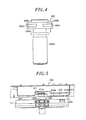
- FIG. 3 is a perspective view schematically showing a configuration of a contact probe and its surroundings shown in FIG. 1 .
- FIG. 4 is a side view schematically showing a configuration of the contact probe shown in FIG. 1 .
- FIG. 5 is a side view schematically showing a configuration of the side of a cleaning unit shown in FIG. 1 .
- FIG. 6 is a bottom view schematically showing a configuration of the bottom of the cleaning unit shown in FIG. 1 .
- FIG. 7 is a flowchart of a cleaning method of the contact probe performed by the probe device of FIG. 1 .
- FIG. 8 is a plan view for explaining a cleaning operation of two contact probes by the cleaning unit shown in FIG. 1 .
- FIG. 9 is a plan view for explaining a cleaning operation of two contact probes by the cleaning unit shown in FIG. 1 .
- FIG. 1 is a plan view schematically showing an entire configuration of a probe device 100 in accordance with an embodiment of the present invention.
- FIG. 2 is a side view schematically showing a configuration of a main part of the probe device 100 of FIG. 1 .
- the probe device 100 mainly includes a measuring unit 110 , a loader unit 150 serving as a transfer unit, and a control unit 600 .
- the entire operation of the probe device 100 is controlled by the control unit 600 having a computer and the like.
- a mounting table 111 on which a semiconductor wafer W is mounted is provided to be movable in x-y-z- ⁇ directions.
- Probes 211 (see FIG. 2 ) installed at a probe card 210 and electrodes of semiconductor devices formed on the semiconductor wafer W are made contact to each other by driving the mounting table 111 by using a driving mechanism 112 , and electrical characteristics of the semiconductor devices are measured.
- a load port 152 on which a wafer carrier (wafer cassette or FOUP) 151 accommodating the semiconductor wafer W is mounted is installed at the front side of the loader unit 150 (lower side in FIG. 1 ), and a wafer transfer mechanism 160 is installed adjacent to the load port 152 .
- a position alignment mechanism 170 is installed at the rear side of the loader unit 150 (upper side in FIG. 1 ). The position alignment mechanism 170 detects a position of a notch of the semiconductor wafer W and an eccentric state of the semiconductor wafer W by rotating the semiconductor wafer W.
- the wafer transfer mechanism 160 includes a wafer transfer arm 161 for vacuum-suctioning and transferring the semiconductor wafer W.
- the wafer transfer arm 161 includes a plurality of (two in this embodiment) suction portions (suction pad) 162 for vacuum-suctioning and holding the semiconductor wafer W.
- a vacuum line (not shown in FIG. 1 ) connected to a suction source such as a vacuum pump is connected to the suction portions 162 .
- the wafer transfer arm 161 may be, if necessary, provided in plural number in a vertically overlapped state.
- the wafer transfer mechanism 160 transfers the semiconductor wafer W between the wafer carrier 151 mounted on the load port 152 , the position alignment mechanism 170 , and the mounting table 111 of the measuring unit 110 by extending, retracting and rotating the wafer transfer arm 161 .
- the load port 152 is movable up and down by a vertical moving mechanism.
- a support frame 153 is provided between the load port 152 and the wafer transfer mechanism 160 .
- An optical detector (not shown) is installed at the support frame 153 . The optical detector detects presense or absence of the semiconductor wafer W while the wafer carrier 151 mounted on the load port 152 is moved up and down. Therefore, it is possible to detect a slot in the wafer carrier 151 which receives the semiconductor wafer W.
- the probe card 210 is disposed above the mounting table 111 and fixed to a head plate 110 A arranged at an upper portion of the measuring unit 110 through a clamp mechanism (not shown).
- a plurality of probes 211 is installed at the probe card 210 and the probes 211 are electrically connected to a tester 300 .
- a conductive film electrode 220 (indicated by a bold line in FIG. 2 ), which is a mounting table electrode, made of conductive metal such as gold or the like is formed on the mounting surface of the mounting table 111 on which the semiconductor wafer W is mounted and on an upper portion of the side surface of the mounting table 111 .
- the conductive film electrode 220 contacts with a backside electrode formed on the backside of the semiconductor device of the mounted semiconductor wafer W.
- a vacuum chuck (not shown) and a temperature control mechanism (not shown) are provided in the mounting table 111 , so that the semiconductor wafer W mounted on the mounting table 111 can be sucked and held and can be controlled to a desired temperature.
- An electrode plate 221 is provided between the probe card 210 and the mounting table 111 .
- the electrode plate 221 is electrically connected to the tester 300 .
- a plurality of (in this embodiment, total two at positions distanced by 180°) contact probes 222 serving as a connection conductor is provided at the side of the mounting table 111 .
- the contact probes 222 are electrically connected to the conductive film electrode 220 .
- the contact probes 222 and the electrode plate 221 are made contact with each other and thus the conductive film electrode 220 and the tester 300 are electrically connected to each other.
- a disk-shaped contact portion 222 a is provided at the apex of the contact probe 222 .
- the top surface of the contact portion 222 a is formed uneven.
- a rectangular parallelepiped-shaped cable connection portion 222 b is provided below the contact portion 222 a .
- the contact portion 222 a and the cable connection portion 222 b are formed integrally and made of metal such as brass or the like. That is, the contact portion 222 a and the cable connection portion 222 b are formed by cutting one metal material.
- a gold-plated layer having a thickness of, e.g., about 0.3 ⁇ m to 0.5 ⁇ m is formed on the surface of the contact portion 222 a and the cable connection portion 222 b .
- An intermediate plated layer made of electroless nickel plating or the like having a thickness of, e.g., about 3 ⁇ m is formed under the gold-plated layer.
- two screw holes 222 c are formed so as to be positioned at opposite end portions in the lengthwise direction of the cable connection portion 222 b at the side wall portions of the cable connection portion 222 b .
- a cylindrical portion 222 d is formed below the cable connection portion 222 b .
- the cylindrical portion 222 d is accommodated in a cylindrical member 222 e .
- the contact portion 222 a , the cable connection portion 222 b and the like are biased toward the upper side with respect to the cylindrical member 222 e by a biasing member (not shown) such as a coil spring provided in the cylindrical member 222 e .
- a biasing member such as a coil spring provided in the cylindrical member 222 e .
- the contact portion 222 a , the cable connection portion 222 b and the like are movable in the vertical direction with respect to the cylindrical member 222 e . Accordingly, the contact portion 222 a contacts with the electrode plate 221 in an elastically pressed state.
- the cable connection portion 222 b is arranged just below the contact portion 222 a of the contact probe 222 . Further, the contact portion 222 a and the cable connection portion 222 b are integrally formed, and no sliding unit for making the contact portion 222 a elastically contact with the electrode plate 221 is interposed between the contact portion 222 a and the cable connection portion 222 b . Furthermore, the gold-plated layer is formed on the surfaces of the contact portion 222 a and the cable connection portion 222 b.
- an electrical path between the contact portion 222 a and the cable connection portion 222 b can be made shorter, thereby suppressing an increase in electric resistance and inductance.
- the cable connection portion 222 b and the conductive film electrode 220 are electrically connected to each other by the short cable 225 having low electric resistance, so that electric resistance between the conductive film electrode 220 and the tester 300 can be greatly reduced compared to a conventional case.
- inductance component can also be reduced.
- a stopper and guide block 226 made of aluminum or the like is fixed to the side wall of the mounting table 111 .
- a base block 227 made of stainless steel or the like is provided protruding from a lower portion of the mounting table 111 .
- the contact probe 222 is locked to the base block 227 through a probe guide block 228 made of, e.g., resin such as PEEK (polyether ether ketone) or the like and a probe presser 229 made of, e.g., aluminum or the like.
- An elevation mechanism 230 for moving the contact probe 222 up and down is provided below the base block 227 .
- the elevation mechanism 230 moves the contact probe 222 up and down between an elevated position and a lowered position when the probes 211 have contacted with the electrodes of the top surface of the semiconductor wafer W by the elevation of the mounting table 111 .
- the contact portion 222 a contacts with the electrode plate 221 and at the lowered position, the contact portion 222 a does not contact with the electrode plate 221 .
- FIG. 5 is a view schematically showing a configuration of the side of the cleaning unit 410 .
- FIG. 6 is a view schematically showing a configuration of the bottom of the cleaning unit 410 .
- a brush unit 411 As shown in FIGS. 5 and 6 , a brush unit 411 , a polishing unit 412 and a contact resistance measuring unit 413 are provided in the cleaning unit 410 .
- the brush unit 411 has a brush 411 a , and performs brush-cleaning by making the brush 411 a contact with the top surface of the contact portion 222 a of the contact probe 222 and rubbing the top surface of the contact portion 222 a with the brush 411 a.
- the polishing unit 412 has a polishing member 412 a made of ceramic or the like.
- the polishing unit 412 polishes the top surface of the contact portion 222 a of the contact probe 222 by making the polishing member 412 a contact with the top surface of the contact portion 222 a and rubbing the top surface of the contact portion 222 a with the polishing member 412 a .
- the contact resistance measuring unit 413 has a contact resistance measuring electrode 413 a , and measures a contact resistance by using a measuring mechanism (not shown) while making the contact resistance measuring electrode 413 a contact with the top surface of the contact portion 222 a of the contact probe 222 .
- the top surface of the contact portion 222 a of the contact probe 222 is made contact with the brush 411 a and rubbed with the brush 411 a by moving the mounting table 111 . By doing so, a brush-cleaning is performed in step S 501 .
- the top surface of the contact portion 222 a of the contact probe 222 is made contact with the contact resistance measuring electrode 413 a by moving the mounting table 111 and the contact resistance of the contact portion 222 a is measured by the measuring mechanism (not shown). It is determined if the measured contact resistance value is equal to or smaller than a predetermined value in step S 502 .
- the predetermined value that is a determination criterion of the contact resistance value may be, e.g., about 1 m ⁇ to 10 m ⁇ , and specifically, e.g., 5 m ⁇ .
- step S 502 when the contact resistance value of the contact probe 222 is larger than the predetermined value (NG in step S 502 ), the top surface of the contact portion 222 a of the contact probe 222 is made contact with the polishing member 412 a and rubbed with the polishing member 412 a by moving the mounting table 111 . By doing so, the top surface of the contact portion 222 a is polished in step S 505 .
- step S 506 the brush-cleaning of the contact portion 222 a of the contact probe 222 is again performed by the brush 411 a in step S 506 .
- the top surface of the contact portion 222 a of the contact probe 222 is again made contact with the contact resistance measuring electrode 413 a and the contact resistance of the contact portion 222 a is measured by the measuring mechanism (not shown). Then, it is determined if the measured contact resistance value is equal to or smaller than the predetermined value in step S 507 .
- step S 507 As a determination result of step S 507 , when the contact resistance value of the contact probe 222 is equal to or smaller than the predetermined value (OK in step S 507 ), a gas is injected to the mounting surface of the mounting table 111 by the gas injection mechanism (not shown) installed at the bridge 400 to thereby perform a chuck blow for removing dust and the like from the mounting surface in step S 503 . Then, the cleaning is completed in step S 504 .
- step S 507 when the contact resistance value of the contact probe 222 is larger than the predetermined value (NG in step S 507 ), the reason that the contact resistance value of the contact probe 222 is large is examined to repair the contact probe 222 in step S 508 and then the step is returned to step S 507 .
- the bridge 400 is first moved to place the cleaning unit 410 above one contact probe 222 , and after a cleaning of the one contact probe 222 is completed, the bridge 400 is further moved to place the cleaning unit 410 above the other contact probe 222 . Then, a cleaning of the other contact probe 222 is performed.
- the wafer carrier 151 accommodating the semiconductor wafers W is mounted on the load port 152 of the loader unit 150 , the wafer carrier 151 is moved up and down by the vertical moving mechanism, and a slot accommodating the semiconductor wafer W is detected by the optical detector.
- the semiconductor wafer W is sucked and held by the wafer transfer arm 161 of the wafer transfer mechanism 160 and transferred to the position alignment mechanism 170 .
- a position of the semiconductor wafer W is detected by detecting a notch of the semiconductor wafer W by the position alignment mechanism 170 .
- the semiconductor wafer W of which the position has been detected by the position alignment mechanism 170 is taken from the position alignment mechanism 170 and mounted on the mounting table 111 of the measuring unit 110 by the wafer transfer arm 161 of the wafer transfer mechanism 160 .
- the probes 211 are made contact with the semiconductor device of the semiconductor wafer W on the mounting table 111 to obtain electrical conduction between the tester 300 and the electrodes of the top surface of the semiconductor wafer W. Further, the contact portion 222 a of the contact probe 222 is made contact with the electrode plate 221 to obtain electrical conduction between the tester 300 and the backside electrode of the semiconductor wafer W.
- a test signal is applied from the tester 300 to the semiconductor device, and an output signal from the semiconductor device is measured. By doing so, an electrical characteristic test of the semiconductor device is performed.
- the semiconductor wafer W is taken and accommodated in the wafer carrier 151 by the wafer transfer arm 161 of the wafer transfer mechanism 160 . Then, the test of the semiconductor wafer W is completed.
- the present invention has been described with respect to the above embodiment, but the present invention is not limited to the above embodiment.
- the contact probe is not limited to the shape shown in FIG. 3 and may use a plurality of pogo pins or may have various shapes.
Abstract
A probe device includes an electrode plate arranged above a mounting table for mounting thereon a semiconductor wafer and electrically connected to a tester, a connection conductor arranged at a side of the mounting table and electrically connected to a mounting table electrode formed on a mounting surface of the mounting table, and a cleaning mechanism including a polishing unit for polishing a contact portion of the connection conductor, a brush cleaning unit for performing a brush-cleaning of the contact portion, and a contact resistance measuring unit for measuring a contact resistance of the contact portion. The mounting table electrode is in contact with a backside electrode of a semiconductor device of the semiconductor wafer. When the connection conductor is connected to the electrode plate, a backside electrode formed on a backside of the semiconductor device and the tester are electrically connected to each other.
Description
This application is a National Stage Application of, and claims priority to, PCT Application No. PCT/JP2014/058151, filed on Mar. 18, 2014, entitled “Probe Device,” which claims priority to Japanese Patent Application No. 2013-067810, filed on Mar. 28, 2013. The foregoing patent applications are herein incorporated by reference by entirety for all purposes.
The present invention relates to a probe device.
In a manufacturing process of a semiconductor device, a probe device is used to perform an electrical test of a semiconductor device formed on a semiconductor wafer. In the probe device, a semiconductor wafer is mounted on a mounting table (chuck top) and electrical conduction is obtained by driving the mounting table to bring probes into contact with electrodes of the semiconductor device of the semiconductor wafer. The test of the semiconductor device is performed by applying a predetermined test signal from a measuring device (tester) to the semiconductor device through the probe and detecting an output signal from the semiconductor device.
In a probe device for performing an electrical test of a semiconductor device having an electrode at the backside of the semiconductor wafer, e.g., a power device having a collector electrode formed at the backside of the semiconductor wafer, a conductive film electrode made of a conductive metal such as gold is formed as a mounting table electrode at a mounting surface of a mounting table (chuck top) and the conductive film electrode is made contact with the electrode formed at the backside of the semiconductor wafer, thereby obtaining electrical conduction. The power device has a high withstand voltage and a high current compared to a general semiconductor device and may have a high speed and a high frequency depending on purpose. An insulated-gate bipolar transistor (IGBT), a diode, a power transistor, a power MOSFET, a thyristor and the like may be used as the power device. The quality of the power device is determined by measuring its electrical characteristic (static characteristic and dynamic characteristic).
Further, in the probe device for performing an electrical test of the power device and the like, if the conductive film electrode and the tester are electrically connected to each other by a cable or the like, the cable becomes longer due to a driving type of the mounting table and this leads to an increase of resistance or inductance of the cable. For this reason, there has been known a probe device having a configuration that a metallic connection conductor electrically connected to the conductive film electrode is provided at a side surface of the mounting table and the connection conductor is made contact with a metallic electrode plate provided above the mounting table to obtain electrical conduction (see, e.g., Patent Document 1).
Patent Document 1: Japanese Patent Application Publication No. 2012-58225.
However, in the probe device having the above configuration, since electrical conduction is obtained by making the metallic connection conductor contact with the metallic electrode plate, metal pieces and the like are generated by the contact and a contact resistance between the connection conductor and the electrode plate gradually increases while the test is performed repeatedly. Accordingly, it may be difficult to perform a test having a high precision.
In view of the above, the present invention provides a probe device capable of performing a test with high precision for a long period of time.
In accordance with an aspect, there is provided a probe device which is electrically connected to a semiconductor device formed on a semiconductor wafer and performs an electrical test of the semiconductor device by a tester, the probe device including: a mounting table configured to mount thereon the semiconductor wafer; a mounting table electrode formed on a mounting surface of the mounting table on which the semiconductor wafer is mounted, the mounting table electrode being in contact with a backside electrode formed on a backside of the semiconductor device; a probe card arranged above the mounting table, the prove card having a plurality of probes electrically connected to the tester; a driving mechanism configured to drive the mounting table to make the probes contact with electrodes of the semiconductor device of the semiconductor wafer mounted on the mounting table; an electrode plate arranged above the mounting table and electrically connected to the tester; a connection conductor arranged at a side of the mounting table and electrically connected to the mounting table electrode, the connection conductor being connectable to the electrode plate, wherein when the connection conductor is connected to the electrode plate, the backside electrode and the tester are electrically connected to each other; and a cleaning mechanism including a polishing unit configured to polish a contact portion of the connection conductor with the electrode plate, a brush cleaning unit configured to perform a brush-cleaning of the contact portion, and a contact resistance measuring unit configured to measure a contact resistance of the contact portion.
In accordance with the present invention, there is provided a probe device capable of performing a test with high precision for a long period of time.
Hereinafter, embodiments of the present invention will be described with respect to the accompanying drawings.
As shown in FIG. 1 , the probe device 100 mainly includes a measuring unit 110, a loader unit 150 serving as a transfer unit, and a control unit 600. The entire operation of the probe device 100 is controlled by the control unit 600 having a computer and the like.
In the measuring unit 110, a mounting table 111 on which a semiconductor wafer W is mounted is provided to be movable in x-y-z-θ directions. Probes 211 (see FIG. 2 ) installed at a probe card 210 and electrodes of semiconductor devices formed on the semiconductor wafer W are made contact to each other by driving the mounting table 111 by using a driving mechanism 112, and electrical characteristics of the semiconductor devices are measured.
A bridge 400 on which an alignment camera (not shown) is mounted is installed above the mounting table 111. The bridge 400 can be driven, in parallel to a mounting surface of the mounting table 111, in forward and backward directions (up-down direction in FIG. 1 ) of the probe device 100. A cleaning unit 410 is installed at the bridge 400. The detail configuration of the cleaning unit 410 will be later described.
A load port 152 on which a wafer carrier (wafer cassette or FOUP) 151 accommodating the semiconductor wafer W is mounted is installed at the front side of the loader unit 150 (lower side in FIG. 1 ), and a wafer transfer mechanism 160 is installed adjacent to the load port 152. A position alignment mechanism 170 is installed at the rear side of the loader unit 150 (upper side in FIG. 1 ). The position alignment mechanism 170 detects a position of a notch of the semiconductor wafer W and an eccentric state of the semiconductor wafer W by rotating the semiconductor wafer W.
The wafer transfer mechanism 160 includes a wafer transfer arm 161 for vacuum-suctioning and transferring the semiconductor wafer W. The wafer transfer arm 161 includes a plurality of (two in this embodiment) suction portions (suction pad) 162 for vacuum-suctioning and holding the semiconductor wafer W. A vacuum line (not shown in FIG. 1 ) connected to a suction source such as a vacuum pump is connected to the suction portions 162. The wafer transfer arm 161 may be, if necessary, provided in plural number in a vertically overlapped state.
The wafer transfer mechanism 160 transfers the semiconductor wafer W between the wafer carrier 151 mounted on the load port 152, the position alignment mechanism 170, and the mounting table 111 of the measuring unit 110 by extending, retracting and rotating the wafer transfer arm 161.
The load port 152 is movable up and down by a vertical moving mechanism. A support frame 153 is provided between the load port 152 and the wafer transfer mechanism 160. An optical detector (not shown) is installed at the support frame 153. The optical detector detects presense or absence of the semiconductor wafer W while the wafer carrier 151 mounted on the load port 152 is moved up and down. Therefore, it is possible to detect a slot in the wafer carrier 151 which receives the semiconductor wafer W.
As shown in FIG. 2 , the probe card 210 is disposed above the mounting table 111 and fixed to a head plate 110A arranged at an upper portion of the measuring unit 110 through a clamp mechanism (not shown). A plurality of probes 211 is installed at the probe card 210 and the probes 211 are electrically connected to a tester 300.
A conductive film electrode 220 (indicated by a bold line in FIG. 2 ), which is a mounting table electrode, made of conductive metal such as gold or the like is formed on the mounting surface of the mounting table 111 on which the semiconductor wafer W is mounted and on an upper portion of the side surface of the mounting table 111. The conductive film electrode 220 contacts with a backside electrode formed on the backside of the semiconductor device of the mounted semiconductor wafer W. A vacuum chuck (not shown) and a temperature control mechanism (not shown) are provided in the mounting table 111, so that the semiconductor wafer W mounted on the mounting table 111 can be sucked and held and can be controlled to a desired temperature.
An electrode plate 221 is provided between the probe card 210 and the mounting table 111. The electrode plate 221 is electrically connected to the tester 300. A plurality of (in this embodiment, total two at positions distanced by 180°) contact probes 222 serving as a connection conductor is provided at the side of the mounting table 111. The contact probes 222 are electrically connected to the conductive film electrode 220. When the mounting table 111 is elevated, the contact probes 222 and the electrode plate 221 are made contact with each other and thus the conductive film electrode 220 and the tester 300 are electrically connected to each other. The electrode plate 221 has a shape that is contactable with the contact probes 222 at any positions when the probes 211 are made contact with the electrodes of the top surface of the semiconductor wafer W by driving the mounting table 111. For example, the electrode plate 221 may have a shape divided by two to allow the annular or two contact probes 222 to contact with the electrode plate 221.
As shown in FIG. 3 , a disk-shaped contact portion 222 a is provided at the apex of the contact probe 222. The top surface of the contact portion 222 a is formed uneven. Below the contact portion 222 a, a rectangular parallelepiped-shaped cable connection portion 222 b is provided. The contact portion 222 a and the cable connection portion 222 b are formed integrally and made of metal such as brass or the like. That is, the contact portion 222 a and the cable connection portion 222 b are formed by cutting one metal material.
A gold-plated layer having a thickness of, e.g., about 0.3 μm to 0.5 μm is formed on the surface of the contact portion 222 a and the cable connection portion 222 b. An intermediate plated layer made of electroless nickel plating or the like having a thickness of, e.g., about 3 μm is formed under the gold-plated layer.
As shown in FIG. 4 , two screw holes 222 c are formed so as to be positioned at opposite end portions in the lengthwise direction of the cable connection portion 222 b at the side wall portions of the cable connection portion 222 b. By screwing screws 223 (see FIG. 3 ) into the screw holes 222 c and screws 224 into screw holes (not shown) formed at the conductive film electrode 220 of the mounting table 111, a conductor of a cable 225 is fixed by the screws 223 and 224 and thus the conductive film electrode 220 and the contact probe 222 are electrically connected to each other.
A cylindrical portion 222 d is formed below the cable connection portion 222 b. The cylindrical portion 222 d is accommodated in a cylindrical member 222 e. The contact portion 222 a, the cable connection portion 222 b and the like are biased toward the upper side with respect to the cylindrical member 222 e by a biasing member (not shown) such as a coil spring provided in the cylindrical member 222 e. As indicated by an arrow in FIG. 4 , the contact portion 222 a, the cable connection portion 222 b and the like are movable in the vertical direction with respect to the cylindrical member 222 e. Accordingly, the contact portion 222 a contacts with the electrode plate 221 in an elastically pressed state.
As described above, in the probe device 100 of the present embodiment, the cable connection portion 222 b is arranged just below the contact portion 222 a of the contact probe 222. Further, the contact portion 222 a and the cable connection portion 222 b are integrally formed, and no sliding unit for making the contact portion 222 a elastically contact with the electrode plate 221 is interposed between the contact portion 222 a and the cable connection portion 222 b. Furthermore, the gold-plated layer is formed on the surfaces of the contact portion 222 a and the cable connection portion 222 b.
Accordingly, an electrical path between the contact portion 222 a and the cable connection portion 222 b can be made shorter, thereby suppressing an increase in electric resistance and inductance. Further, the cable connection portion 222 b and the conductive film electrode 220 are electrically connected to each other by the short cable 225 having low electric resistance, so that electric resistance between the conductive film electrode 220 and the tester 300 can be greatly reduced compared to a conventional case. Furthermore, since an electrical path from the conductive film electrode 220 to the contact portion 222 a is short, inductance component can also be reduced.
As shown in FIG. 3 , a stopper and guide block 226 made of aluminum or the like is fixed to the side wall of the mounting table 111. A base block 227 made of stainless steel or the like is provided protruding from a lower portion of the mounting table 111. The contact probe 222 is locked to the base block 227 through a probe guide block 228 made of, e.g., resin such as PEEK (polyether ether ketone) or the like and a probe presser 229 made of, e.g., aluminum or the like.
An elevation mechanism 230 for moving the contact probe 222 up and down is provided below the base block 227. The elevation mechanism 230 moves the contact probe 222 up and down between an elevated position and a lowered position when the probes 211 have contacted with the electrodes of the top surface of the semiconductor wafer W by the elevation of the mounting table 111. At the elevated position, the contact portion 222 a contacts with the electrode plate 221 and at the lowered position, the contact portion 222 a does not contact with the electrode plate 221.
The elevation mechanism 230 can change a position in the vertical direction of the contact probe 22 in multi-steps between the elevated position and the lowered position. By doing so, a contact state between the contact portion 222 a and the electrode plate 221 can be adjusted to an optimal state.
The polishing unit 412 has a polishing member 412 a made of ceramic or the like. The polishing unit 412 polishes the top surface of the contact portion 222 a of the contact probe 222 by making the polishing member 412 a contact with the top surface of the contact portion 222 a and rubbing the top surface of the contact portion 222 a with the polishing member 412 a. The contact resistance measuring unit 413 has a contact resistance measuring electrode 413 a, and measures a contact resistance by using a measuring mechanism (not shown) while making the contact resistance measuring electrode 413 a contact with the top surface of the contact portion 222 a of the contact probe 222.
Next, a cleaning method of the contact probe 222 by the cleaning unit 410 having the above configuration will be described with reference to a flowchart of FIG. 7 . The cleaning method to be described hereinafter is performed under a control of the control unit 600 shown in FIG. 1 .
In the cleaning method of the contact probe 222 in accordance with the present embodiment, first, the top surface of the contact portion 222 a of the contact probe 222 is made contact with the brush 411 a and rubbed with the brush 411 a by moving the mounting table 111. By doing so, a brush-cleaning is performed in step S501.
Thereafter, the top surface of the contact portion 222 a of the contact probe 222 is made contact with the contact resistance measuring electrode 413 a by moving the mounting table 111 and the contact resistance of the contact portion 222 a is measured by the measuring mechanism (not shown). It is determined if the measured contact resistance value is equal to or smaller than a predetermined value in step S502. In this case, the predetermined value that is a determination criterion of the contact resistance value may be, e.g., about 1 mΩ to 10 mΩ, and specifically, e.g., 5 mΩ.
As a determination result of step S502, when the contact resistance value of the contact probe 222 is equal to or smaller than the predetermined value (OK in step S502), a gas is injected to the mounting surface of the mounting table 111 by a gas injection mechanism (not shown) installed at the bridge 400 to thereby perform a chuck blow for removing dust and the like from the mounting surface in step S503. Then, the cleaning is completed in step S504.
On the other hand, as a determination result of step S502, when the contact resistance value of the contact probe 222 is larger than the predetermined value (NG in step S502), the top surface of the contact portion 222 a of the contact probe 222 is made contact with the polishing member 412 a and rubbed with the polishing member 412 a by moving the mounting table 111. By doing so, the top surface of the contact portion 222 a is polished in step S505.
Subsequently, after completing the polishing of the top surface of the contact portion 222 a by the polishing member 412 a, the brush-cleaning of the contact portion 222 a of the contact probe 222 is again performed by the brush 411 a in step S506.
Thereafter, the top surface of the contact portion 222 a of the contact probe 222 is again made contact with the contact resistance measuring electrode 413 a and the contact resistance of the contact portion 222 a is measured by the measuring mechanism (not shown). Then, it is determined if the measured contact resistance value is equal to or smaller than the predetermined value in step S507.
As a determination result of step S507, when the contact resistance value of the contact probe 222 is equal to or smaller than the predetermined value (OK in step S507), a gas is injected to the mounting surface of the mounting table 111 by the gas injection mechanism (not shown) installed at the bridge 400 to thereby perform a chuck blow for removing dust and the like from the mounting surface in step S503. Then, the cleaning is completed in step S504.
On the other hand, as a determination result of the step S507, when the contact resistance value of the contact probe 222 is larger than the predetermined value (NG in step S507), the reason that the contact resistance value of the contact probe 222 is large is examined to repair the contact probe 222 in step S508 and then the step is returned to step S507.
As described above, in the present embodiment, the cleaning of the contact probe 222 is performed by the cleaning unit 410. Accordingly, the contact resistance value of the contact probe 222 is always maintained at a low value equal to or smaller than the predetermined value for a long period of time, and thus a test can be performed with high precision for a long period of time.
In the probe device 100 of the present embodiment, since two contact probes 222 are provided, as shown in FIGS. 8 and 9 , the bridge 400 is first moved to place the cleaning unit 410 above one contact probe 222, and after a cleaning of the one contact probe 222 is completed, the bridge 400 is further moved to place the cleaning unit 410 above the other contact probe 222. Then, a cleaning of the other contact probe 222 is performed.
Next, a test sequence of the semiconductor wafer W by the probe device 100 will be described.
First, if the wafer carrier 151 accommodating the semiconductor wafers W is mounted on the load port 152 of the loader unit 150, the wafer carrier 151 is moved up and down by the vertical moving mechanism, and a slot accommodating the semiconductor wafer W is detected by the optical detector.
Next, the semiconductor wafer W is sucked and held by the wafer transfer arm 161 of the wafer transfer mechanism 160 and transferred to the position alignment mechanism 170. A position of the semiconductor wafer W is detected by detecting a notch of the semiconductor wafer W by the position alignment mechanism 170.
Next, the semiconductor wafer W of which the position has been detected by the position alignment mechanism 170 is taken from the position alignment mechanism 170 and mounted on the mounting table 111 of the measuring unit 110 by the wafer transfer arm 161 of the wafer transfer mechanism 160.
Then, the probes 211 are made contact with the semiconductor device of the semiconductor wafer W on the mounting table 111 to obtain electrical conduction between the tester 300 and the electrodes of the top surface of the semiconductor wafer W. Further, the contact portion 222 a of the contact probe 222 is made contact with the electrode plate 221 to obtain electrical conduction between the tester 300 and the backside electrode of the semiconductor wafer W. In this state, a test signal is applied from the tester 300 to the semiconductor device, and an output signal from the semiconductor device is measured. By doing so, an electrical characteristic test of the semiconductor device is performed.
When the electrical characteristic test of the semiconductor device of the semiconductor wafer W is completed, the semiconductor wafer W is taken and accommodated in the wafer carrier 151 by the wafer transfer arm 161 of the wafer transfer mechanism 160. Then, the test of the semiconductor wafer W is completed.
As above, the present invention has been described with respect to the above embodiment, but the present invention is not limited to the above embodiment. For example, the contact probe is not limited to the shape shown in FIG. 3 and may use a plurality of pogo pins or may have various shapes.
The present application claims priority based on Japanese Patent Application No. 2013-067810 filed on Mar. 28, 2013, the entire contents of which are incorporated herein by reference.
- W semiconductor wafer
- 100 probe device
- 111 mounting table
- 112 driving mechanism
- 210 probe card
- 211 probe
- 220 conductive film electrode
- 221 electrode plate
- 222 contact probe
- 300 tester
- 410 cleaning unit
- 412 polishing unit
- 411 brush unit
- 413 contact resistance measuring unit
Claims (4)
1. A probe device which is electrically connected to a semiconductor device formed on a semiconductor wafer and performs an electrical test of the semiconductor device by a tester, the probe device comprising:
a mounting table configured to mount thereon the semiconductor wafer;
a mounting table electrode formed on a mounting surface of the mounting table on which the semiconductor wafer is mounted, the mounting table electrode being in contact with a backside electrode formed on a backside of the semiconductor device;
a probe card arranged above the mounting table, the prove card having a plurality of probes electrically connected to the tester;
a driving mechanism configured to drive the mounting table to make the probes contact with electrodes of the semiconductor device of the semiconductor wafer mounted on the mounting table;
an electrode plate arranged above the mounting table and electrically connected to the tester;
a connection conductor arranged at a side of the mounting table and electrically connected to the mounting table electrode, the connection conductor being connectable to the electrode plate, wherein when the connection conductor is connected to the electrode plate, the backside electrode and the tester are electrically connected to each other; and
a cleaning mechanism including a polishing unit configured to polish a contact portion of the connection conductor with the electrode plate, a brush cleaning unit configured to perform a brush-cleaning of the contact portion, and a contact resistance measuring unit configured to measure a contact resistance of the contact portion.
2. The probe device of claim 1 , wherein the cleaning mechanism performs the brush-cleaning of the contact portion by the brush cleaning unit, measures the contact resistance of the contact portion by the contact resistance measuring unit, and when a measured value of the contact resistance is equal to or larger than a set value, polishes the contact portion by the polishing unit.
3. The probe device of claim 1 , wherein the connection conductor is arranged in plural number at an interval along a circumferential direction of the mounting table.
4. The probe device of claim 1 , wherein the cleaning mechanism is arranged above the mounting table and moved in parallel to the mounting surface.
Applications Claiming Priority (3)
| Application Number | Priority Date | Filing Date | Title |
|---|---|---|---|
| JP2013067810A JP6042760B2 (en) | 2013-03-28 | 2013-03-28 | Probe device |
| JP2013-067810 | 2013-03-28 | ||
| PCT/JP2014/058151 WO2014157122A1 (en) | 2013-03-28 | 2014-03-18 | Probe device |
Publications (2)
| Publication Number | Publication Date |
|---|---|
| US20160054357A1 US20160054357A1 (en) | 2016-02-25 |
| US9638719B2 true US9638719B2 (en) | 2017-05-02 |
Family
ID=51624094
Family Applications (1)
| Application Number | Title | Priority Date | Filing Date |
|---|---|---|---|
| US14/781,003 Active 2034-03-21 US9638719B2 (en) | 2013-03-28 | 2014-03-18 | Probe device having cleaning mechanism for cleaning connection conductor |
Country Status (6)
| Country | Link |
|---|---|
| US (1) | US9638719B2 (en) |
| EP (1) | EP2980839B1 (en) |
| JP (1) | JP6042760B2 (en) |
| KR (1) | KR101785820B1 (en) |
| TW (1) | TWI632382B (en) |
| WO (1) | WO2014157122A1 (en) |
Cited By (1)
| Publication number | Priority date | Publication date | Assignee | Title |
|---|---|---|---|---|
| US20220206058A1 (en) * | 2019-05-28 | 2022-06-30 | Tokyo Electron Limited | Transport system, inspection system, and inspection method |
Families Citing this family (3)
| Publication number | Priority date | Publication date | Assignee | Title |
|---|---|---|---|---|
| JP6885456B2 (en) * | 2017-02-22 | 2021-06-16 | 新東工業株式会社 | Test system |
| CN110275049A (en) * | 2018-03-14 | 2019-09-24 | 均豪精密工业股份有限公司 | Probe card clear needle method and its system automatically |
| KR102278752B1 (en) * | 2019-11-14 | 2021-07-19 | 주식회사 씨케이엘 | Apparatus for probing semiconductor chip |
Citations (10)
| Publication number | Priority date | Publication date | Assignee | Title |
|---|---|---|---|---|
| US4918374A (en) * | 1988-10-05 | 1990-04-17 | Applied Precision, Inc. | Method and apparatus for inspecting integrated circuit probe cards |
| US5060371A (en) * | 1988-10-05 | 1991-10-29 | Applied Precision, Inc. | Method of making probe cards |
| US5778485A (en) * | 1995-01-19 | 1998-07-14 | Tokyo Electron Limited | Probe card cleaning apparatus, probe apparatus with the cleaning apparatus, and probe card cleaning method |
| JPH1154574A (en) | 1997-06-07 | 1999-02-26 | Tokyo Electron Ltd | Cleaning method and probe |
| JP2000338152A (en) * | 1999-05-31 | 2000-12-08 | Texas Instr Japan Ltd | Method for measuring contact resistance of probe |
| US6765401B2 (en) * | 2002-05-28 | 2004-07-20 | Fujitsu Limited | Semiconductor testing apparatus for conducting conduction tests |
| US6817052B2 (en) * | 2001-11-09 | 2004-11-16 | Formfactor, Inc. | Apparatuses and methods for cleaning test probes |
| US6927078B2 (en) * | 2002-08-27 | 2005-08-09 | Oki Electric Industry Co., Ltd. | Method of measuring contact resistance of probe and method of testing semiconductor device |
| US7250779B2 (en) * | 2002-11-25 | 2007-07-31 | Cascade Microtech, Inc. | Probe station with low inductance path |
| JP2012058225A (en) | 2010-03-12 | 2012-03-22 | Tokyo Electron Ltd | Probe apparatus |
Family Cites Families (9)
| Publication number | Priority date | Publication date | Assignee | Title |
|---|---|---|---|---|
| US6118290A (en) * | 1997-06-07 | 2000-09-12 | Tokyo Electron Limited | Prober and method for cleaning probes provided therein |
| JPH1154572A (en) * | 1997-07-31 | 1999-02-26 | Tokyo Electron Ltd | Probe device |
| JP3429995B2 (en) * | 1997-11-10 | 2003-07-28 | 東京エレクトロン株式会社 | Cleaning method |
| WO2004070405A1 (en) * | 2003-02-05 | 2004-08-19 | Systems On Silicon Manufacturing Co. Pte. Ltd. | Probe card needle cleaning frequency optimization |
| US7345466B2 (en) * | 2005-08-02 | 2008-03-18 | Electroglas, Inc. | Method and apparatus for cleaning a probe card |
| JP3947795B2 (en) * | 2005-12-27 | 2007-07-25 | 東京エレクトロン株式会社 | Cleaning member and probe device |
| US7474089B2 (en) | 2006-12-28 | 2009-01-06 | Texas Instruments Incorporated | Contact mechanism cleaning |
| CN102099699B (en) * | 2008-07-18 | 2014-05-07 | 日本电产丽德株式会社 | Substrate-inspecting device having cleaning mechanism for tips of pins |
| JP5291157B2 (en) * | 2011-08-01 | 2013-09-18 | 東京エレクトロン株式会社 | Probe card for power devices |
-
2013
- 2013-03-28 JP JP2013067810A patent/JP6042760B2/en not_active Expired - Fee Related
-
2014
- 2014-03-18 EP EP14776195.1A patent/EP2980839B1/en active Active
- 2014-03-18 KR KR1020157026585A patent/KR101785820B1/en active IP Right Grant
- 2014-03-18 WO PCT/JP2014/058151 patent/WO2014157122A1/en active Application Filing
- 2014-03-18 US US14/781,003 patent/US9638719B2/en active Active
- 2014-03-20 TW TW103110461A patent/TWI632382B/en active
Patent Citations (12)
| Publication number | Priority date | Publication date | Assignee | Title |
|---|---|---|---|---|
| US4918374A (en) * | 1988-10-05 | 1990-04-17 | Applied Precision, Inc. | Method and apparatus for inspecting integrated circuit probe cards |
| US5060371A (en) * | 1988-10-05 | 1991-10-29 | Applied Precision, Inc. | Method of making probe cards |
| US5778485A (en) * | 1995-01-19 | 1998-07-14 | Tokyo Electron Limited | Probe card cleaning apparatus, probe apparatus with the cleaning apparatus, and probe card cleaning method |
| JPH1154574A (en) | 1997-06-07 | 1999-02-26 | Tokyo Electron Ltd | Cleaning method and probe |
| JP2000338152A (en) * | 1999-05-31 | 2000-12-08 | Texas Instr Japan Ltd | Method for measuring contact resistance of probe |
| US6817052B2 (en) * | 2001-11-09 | 2004-11-16 | Formfactor, Inc. | Apparatuses and methods for cleaning test probes |
| US6765401B2 (en) * | 2002-05-28 | 2004-07-20 | Fujitsu Limited | Semiconductor testing apparatus for conducting conduction tests |
| US6927078B2 (en) * | 2002-08-27 | 2005-08-09 | Oki Electric Industry Co., Ltd. | Method of measuring contact resistance of probe and method of testing semiconductor device |
| US7250779B2 (en) * | 2002-11-25 | 2007-07-31 | Cascade Microtech, Inc. | Probe station with low inductance path |
| JP2012058225A (en) | 2010-03-12 | 2012-03-22 | Tokyo Electron Ltd | Probe apparatus |
| KR20120128159A (en) | 2010-03-12 | 2012-11-26 | 도쿄엘렉트론가부시키가이샤 | Probe apparatus |
| US20130063171A1 (en) | 2010-03-12 | 2013-03-14 | Tokyo Electron Limited | Probe apparatus |
Non-Patent Citations (1)
| Title |
|---|
| The International Search Report. |
Cited By (1)
| Publication number | Priority date | Publication date | Assignee | Title |
|---|---|---|---|---|
| US20220206058A1 (en) * | 2019-05-28 | 2022-06-30 | Tokyo Electron Limited | Transport system, inspection system, and inspection method |
Also Published As
| Publication number | Publication date |
|---|---|
| US20160054357A1 (en) | 2016-02-25 |
| EP2980839A4 (en) | 2016-11-30 |
| EP2980839A1 (en) | 2016-02-03 |
| KR20150138213A (en) | 2015-12-09 |
| TWI632382B (en) | 2018-08-11 |
| WO2014157122A1 (en) | 2014-10-02 |
| KR101785820B1 (en) | 2017-10-16 |
| EP2980839B1 (en) | 2020-10-21 |
| JP2014192404A (en) | 2014-10-06 |
| TW201506421A (en) | 2015-02-16 |
| JP6042760B2 (en) | 2016-12-14 |
Similar Documents
| Publication | Publication Date | Title |
|---|---|---|
| US9638719B2 (en) | Probe device having cleaning mechanism for cleaning connection conductor | |
| US9658285B2 (en) | Probe apparatus | |
| JP5265746B2 (en) | Probe device | |
| US9759762B2 (en) | Probe device | |
| JP5432700B2 (en) | Semiconductor device inspection equipment | |
| JP6674103B2 (en) | Prober | |
| EP2833158A1 (en) | Probe apparatus | |
| TW201539004A (en) | Systems and methods for on-wafer dynamic testing of electronic devices | |
| TW201534945A (en) | Inspection system for device to be tested, and method for operating inspection system for device to be tested | |
| JP2021128065A (en) | Test method for semiconductor device | |
| TW201337287A (en) | Probe probing force setting method and probing method and system using the method | |
| US11307247B2 (en) | Prober with busbar mechanism for testing a device under test | |
| JP6361975B2 (en) | Prober | |
| JP6365953B1 (en) | Prober | |
| US9739828B2 (en) | Probe device | |
| JP2013219269A (en) | Characteristic evaluation device of semiconductor device | |
| JP3895584B2 (en) | Needle polishing tool recognition method and needle polishing tool recognition device | |
| TWI221199B (en) | Probing method, testing apparatus and testing method of semiconductor device | |
| JP6201383B2 (en) | Semiconductor measurement method | |
| JPH04342150A (en) | Inspection of semiconductor device |
Legal Events
| Date | Code | Title | Description |
|---|---|---|---|
| AS | Assignment |
Owner name: TOKYO ELECTRON LIMITED, JAPAN Free format text: ASSIGNMENT OF ASSIGNORS INTEREST;ASSIGNORS:SHINOHARA, EIICHI;NAGASAKA, MUNETOSHI;KATO, YOSHIYASU;REEL/FRAME:036673/0899 Effective date: 20150902 |
|
| STCF | Information on status: patent grant |
Free format text: PATENTED CASE |
|
| MAFP | Maintenance fee payment |
Free format text: PAYMENT OF MAINTENANCE FEE, 4TH YEAR, LARGE ENTITY (ORIGINAL EVENT CODE: M1551); ENTITY STATUS OF PATENT OWNER: LARGE ENTITY Year of fee payment: 4 |