US9643357B2 - Electrophotography-based additive manufacturing with powder density detection and utilization - Google Patents
Electrophotography-based additive manufacturing with powder density detection and utilization Download PDFInfo
- Publication number
- US9643357B2 US9643357B2 US14/218,114 US201414218114A US9643357B2 US 9643357 B2 US9643357 B2 US 9643357B2 US 201414218114 A US201414218114 A US 201414218114A US 9643357 B2 US9643357 B2 US 9643357B2
- Authority
- US
- United States
- Prior art keywords
- transfer belt
- developed
- capacitance
- belt
- layer
- Prior art date
- Legal status (The legal status is an assumption and is not a legal conclusion. Google has not performed a legal analysis and makes no representation as to the accuracy of the status listed.)
- Active, expires
Links
Images


Classifications
-
- G—PHYSICS
- G03—PHOTOGRAPHY; CINEMATOGRAPHY; ANALOGOUS TECHNIQUES USING WAVES OTHER THAN OPTICAL WAVES; ELECTROGRAPHY; HOLOGRAPHY
- G03G—ELECTROGRAPHY; ELECTROPHOTOGRAPHY; MAGNETOGRAPHY
- G03G15/00—Apparatus for electrographic processes using a charge pattern
- G03G15/14—Apparatus for electrographic processes using a charge pattern for transferring a pattern to a second base
- G03G15/16—Apparatus for electrographic processes using a charge pattern for transferring a pattern to a second base of a toner pattern, e.g. a powder pattern, e.g. magnetic transfer
- G03G15/1625—Apparatus for electrographic processes using a charge pattern for transferring a pattern to a second base of a toner pattern, e.g. a powder pattern, e.g. magnetic transfer on a base other than paper
-
- B29C67/0051—
-
- G—PHYSICS
- G01—MEASURING; TESTING
- G01N—INVESTIGATING OR ANALYSING MATERIALS BY DETERMINING THEIR CHEMICAL OR PHYSICAL PROPERTIES
- G01N27/00—Investigating or analysing materials by the use of electric, electrochemical, or magnetic means
- G01N27/02—Investigating or analysing materials by the use of electric, electrochemical, or magnetic means by investigating impedance
- G01N27/22—Investigating or analysing materials by the use of electric, electrochemical, or magnetic means by investigating impedance by investigating capacitance
-
- G—PHYSICS
- G01—MEASURING; TESTING
- G01R—MEASURING ELECTRIC VARIABLES; MEASURING MAGNETIC VARIABLES
- G01R1/00—Details of instruments or arrangements of the types included in groups G01R5/00 - G01R13/00 and G01R31/00
- G01R1/02—General constructional details
- G01R1/18—Screening arrangements against electric or magnetic fields, e.g. against earth's field
-
- G—PHYSICS
- G03—PHOTOGRAPHY; CINEMATOGRAPHY; ANALOGOUS TECHNIQUES USING WAVES OTHER THAN OPTICAL WAVES; ELECTROGRAPHY; HOLOGRAPHY
- G03G—ELECTROGRAPHY; ELECTROPHOTOGRAPHY; MAGNETOGRAPHY
- G03G15/00—Apparatus for electrographic processes using a charge pattern
- G03G15/22—Apparatus for electrographic processes using a charge pattern involving the combination of more than one step according to groups G03G13/02 - G03G13/20
- G03G15/221—Machines other than electrographic copiers, e.g. electrophotographic cameras, electrostatic typewriters
- G03G15/224—Machines for forming tactile or three dimensional images by electrographic means, e.g. braille, 3d printing
-
- G—PHYSICS
- G03—PHOTOGRAPHY; CINEMATOGRAPHY; ANALOGOUS TECHNIQUES USING WAVES OTHER THAN OPTICAL WAVES; ELECTROGRAPHY; HOLOGRAPHY
- G03G—ELECTROGRAPHY; ELECTROPHOTOGRAPHY; MAGNETOGRAPHY
- G03G15/00—Apparatus for electrographic processes using a charge pattern
- G03G15/22—Apparatus for electrographic processes using a charge pattern involving the combination of more than one step according to groups G03G13/02 - G03G13/20
- G03G15/24—Apparatus for electrographic processes using a charge pattern involving the combination of more than one step according to groups G03G13/02 - G03G13/20 whereby at least two steps are performed simultaneously
-
- B—PERFORMING OPERATIONS; TRANSPORTING
- B29—WORKING OF PLASTICS; WORKING OF SUBSTANCES IN A PLASTIC STATE IN GENERAL
- B29L—INDEXING SCHEME ASSOCIATED WITH SUBCLASS B29C, RELATING TO PARTICULAR ARTICLES
- B29L2031/00—Other particular articles
-
- B—PERFORMING OPERATIONS; TRANSPORTING
- B33—ADDITIVE MANUFACTURING TECHNOLOGY
- B33Y—ADDITIVE MANUFACTURING, i.e. MANUFACTURING OF THREE-DIMENSIONAL [3-D] OBJECTS BY ADDITIVE DEPOSITION, ADDITIVE AGGLOMERATION OR ADDITIVE LAYERING, e.g. BY 3-D PRINTING, STEREOLITHOGRAPHY OR SELECTIVE LASER SINTERING
- B33Y10/00—Processes of additive manufacturing
-
- B—PERFORMING OPERATIONS; TRANSPORTING
- B33—ADDITIVE MANUFACTURING TECHNOLOGY
- B33Y—ADDITIVE MANUFACTURING, i.e. MANUFACTURING OF THREE-DIMENSIONAL [3-D] OBJECTS BY ADDITIVE DEPOSITION, ADDITIVE AGGLOMERATION OR ADDITIVE LAYERING, e.g. BY 3-D PRINTING, STEREOLITHOGRAPHY OR SELECTIVE LASER SINTERING
- B33Y30/00—Apparatus for additive manufacturing; Details thereof or accessories therefor
-
- G—PHYSICS
- G03—PHOTOGRAPHY; CINEMATOGRAPHY; ANALOGOUS TECHNIQUES USING WAVES OTHER THAN OPTICAL WAVES; ELECTROGRAPHY; HOLOGRAPHY
- G03G—ELECTROGRAPHY; ELECTROPHOTOGRAPHY; MAGNETOGRAPHY
- G03G2215/00—Apparatus for electrophotographic processes
- G03G2215/16—Transferring device, details
- G03G2215/1676—Simultaneous toner image transfer and fixing
- G03G2215/1695—Simultaneous toner image transfer and fixing at the second or higher order transfer point
Definitions
- the present disclosure relates to additive manufacturing systems and processes for printing three-dimensional (3D) parts and support structures.
- the present disclosure relates to additive manufacturing systems and processes for building 3D parts and support structures using an imaging process, such as electrophotography.
- Additive manufacturing systems are used to build 3D parts from digital representations of the 3D parts (e.g., AMF and STL format files) using one or more additive manufacturing techniques.
- additive manufacturing techniques include extrusion-based techniques, ink jetting, selective laser sintering, powder/binder jetting, electron-beam melting, and stereolithographic processes.
- the digital representation of the 3D part is initially sliced into multiple horizontal layers.
- a tool path is then generated, which provides instructions for the particular additive manufacturing system to form the given layer.
- a 3D part or model may be printed from a digital representation of the 3D part in a layer-by-layer manner by extruding a flowable part material.
- the part material is extruded through an extrusion tip carried by a print head of the system, and is deposited as a sequence of roads on a substrate in an x-y plane.
- the extruded part material fuses to previously deposited part material, and solidifies upon a drop in temperature.
- the position of the print head relative to the substrate is then incremented along a z-axis (perpendicular to the x-y plane), and the process is then repeated to form a 3D part resembling the digital representation.
- supporting layers or structures are typically built underneath overhanging portions or in cavities of objects under construction, which are not supported by the part material itself.
- a support structure may be built utilizing the same deposition techniques by which the part material is deposited.
- the host computer generates additional geometry acting as a support structure for the overhanging or free-space segments of the 3D part being formed, and in some cases, for the sidewalls of the 3D part being formed.
- the support material adheres to the part material during fabrication, and is removable from the completed 3D part when the printing process is complete.
- Electrophotography In two-dimensional (2D) printing, electrophotography (i.e., xerography) is a technology for creating 2D images on planar substrates, such as printing paper and transparent substrates.
- Electrophotography systems typically include a conductive support drum coated with a photoconductive material layer, where latent electrostatic images are formed by electrostatic charging, followed by image-wise exposure of the photoconductive layer by an optical source. The latent electrostatic images are then moved to a developing station where toner is applied to charged areas, or alternatively to discharged areas of the photoconductive insulator to form visible images. The formed toner images are then transferred to substrates (e.g., printing paper) and affixed to the substrates with heat and/or pressure.
- substrates e.g., printing paper
- An aspect of the present disclosure is directed to an additive manufacturing system for printing a 3D part.
- the system includes one or more electrophotography engines configured to develop layers of the 3D part, and a rotatable transfer belt configured to receive the developed layers from the electrophotography engine(s).
- the system also includes a detector configured to measure powder densities of the developed layers on the rotatable transfer belt, and to transmit signals relating to the measured powder densities to a controller assembly of the system.
- the system includes a printing assembly (e.g., a layer transfusion assembly) configured to receive the developed layer from the rotatable transfer belt and to print the 3D part from the developed layers.
- Another aspect of the present disclosure is directed to a method for printing a 3D part with an additive manufacturing system.
- the method includes producing a developed layer of a part material with an electrophotography engine of the additive manufacturing system, and transferring the developed layer from the electrophotography engine to a transfer belt of the additive manufacturing system.
- the method also includes rotating the transfer belt with the developed layer, measuring a powder density of the developed layer on the rotating transfer belt, heating the developed layer on the rotating transfer belt after measuring the powder density, and pressing the heated developed layer into contact with a top surface of the 3D part.
- Another aspect of the present disclosure is directed to a method for measuring a powder density of a developed layer, and utilizing the measured part density, in an additive manufacturing system.
- the method includes rotating a transfer belt of the additive manufacturing system, measuring one or more capacitance values of the rotating transfer belt in a clean state, and determining a baseline capacitance value from the one or more measured capacitance values for the rotating transfer belt.
- the method also includes producing the developed layer of a powder-based material with an electrophotography engine of the additive manufacturing system, transferring the developed layer from the electrophotography engine to the rotating transfer belt, and measuring one or more capacitance values of the developed layer on the rotating transfer belt.
- the method further includes determining a sample capacitance value the one or more measured capacitance values for the developed layer on the rotating transfer belt, and determining a difference between the sample capacitance value and the baseline capacitance value.
- Directional orientations such as “above”, “below”, “top”, “bottom”, and the like are made with reference to a direction along a printing axis of a 3D part.
- the layer-printing direction is the upward direction along the vertical z-axis.
- the terms “above”, “below”, “top”, “bottom”, and the like are based on the vertical z-axis.
- the terms “above”, “below”, “top”, “bottom”, and the like are relative to the given axis.
- providing such as for “providing a material” and the like, when recited in the claims, is not intended to require any particular delivery or receipt of the provided item. Rather, the term “providing” is merely used to recite items that will be referred to in subsequent elements of the claim(s), for purposes of clarity and ease of readability.
- temperatures referred to herein are based on atmospheric pressure (i.e. one atmosphere).
- FIG. 1 is a front view of an example electrophotography-based additive manufacturing system for printing 3D parts and support structures with the use of a powder-density detector.
- FIG. 2 is a schematic front view of a pair of electrophotography engines of the system for developing layers of the part and support materials.
- FIG. 3 is a schematic front view of an alternative electrophotography engine, which includes an intermediary drum or belt.
- FIG. 4 is a schematic front view of a layer transfusion assembly of the system for performing layer transfusion steps with the developed layers.
- FIG. 5 is a bottom perspective view of the powder-density detector disposed along a rotatable transfer belt of the system.
- FIG. 6 is a bottom view of the powder-density detector and the rotatable transfer belt, where a control board of the powder-density detector is schematically illustrated.
- FIG. 7 is a side view of the powder-density detector in use with the rotatable transfer belt.
- FIG. 8 is a schematic illustration of a controller assembly of the system in use with electrophotography engines and the powder-density detector.
- FIG. 9 is a front perspective view of a portion of an electrophotography engine, illustrating an imager and development drum of the electrophotography engine.
- the present disclosure is directed to an electrophotography-based additive manufacturing system and process for measuring powder densities for developed layers of part and support materials.
- one or more electrophotography (EP) engines may develop or otherwise image each layer of part and support materials using an electrophotographic process.
- the developed layers are then transferred to a layer transfusion assembly where they are transfused (e.g., using heat and/or pressure) to print one or more 3D parts and support structures in a layer-by-layer manner.
- the part and support materials are powder-based materials charged triboelectrically through the mechanism of frictional-contact charging with carrier particles.
- This charging of the part or support material may be referred to by its triboelectric charge-to-mass (Q/M) ratio, which may be a positive or negative charge and has a desired magnitude.
- Q/M ratio is inversely proportional to the powder density of the part or support material, which can be referred to by its mass per unit area (M/A) value.
- M/A value mass per unit area
- the powder density or M/A value is preferably maintained at a stable level during an entire printing operation.
- the powder densities of the developed layers can potentially fluctuate or otherwise drift from their intended levels.
- the system discussed herein incorporates one or more detectors that measure the powder densities of developed layers during printing operations, preferably with the use of electrical fields, as discussed below.
- the detector(s) may then transmit signals to a controller assembly of the system, which may monitor the corresponding M/A values in order to identify any changes from the intended levels.
- FIGS. 1-4 illustrate system 10 , which is an example electrophotography-based additive manufacturing system for printing 3D parts from a part material, and associated support structures from a support material, and is designed to measure powder densities of developed layers during printing operations.
- system 10 includes a pair of EP engines 12 p and 12 s , belt transfer assembly 14 , biasing mechanisms 16 and 18 , and layer transfusion assembly 20 .
- suitable components and functional operations for system 10 include those disclosed in Hanson et al., U.S. Publication Nos. 2013/0077996 and 2013/0077997, in Comb et al., U.S. Publication Nos. 2013/0186549 and 2013/0186558.
- EP engines 12 p and 12 s are imaging engines for respectively imaging or otherwise developing layers of the powder-based part and support materials. As discussed below, the imaged layers may then be transferred to belt transfer assembly 14 (or other transfer medium) with biasing mechanisms 16 and 18 , and carried to layer transfusion assembly 20 to print the 3D parts and associated support structures in a layer-by-layer manner.
- belt transfer assembly 14 includes transfer belt 22 , belt drive mechanisms 24 , belt drag mechanisms 26 , loop limit sensors 28 , idler rollers 30 , and belt cleaner 32 , which are configured to maintain tension on belt 22 while belt 22 rotates in the rotational direction of arrows 34 .
- belt drive mechanisms 24 engage and drive belt 22
- belt drag mechanisms 26 may function as brakes to provide a service loop design for protecting belt 22 against tension stress, based on monitored readings via loop limit sensors 28 .
- the components of system 10 may be retained by one or more frame structures, such as frame 36 . Additionally, the components of system 10 are preferably retained within an enclosable housing (not shown) that prevents ambient light from being transmitted to the components of system 10 during operation.
- System 10 also includes detector 38 and controller assembly 40 , where detector 38 is an example non-contact detector for measuring powder densities of developed layers, as discussed below.
- detector 38 is positioned along belt 22 downstream from EP engine 12 p and the first idler roller 30 , and upstream from the first belt drive mechanism 24 .
- One or more detectors 38 may alternatively be located at any suitable point along belt 22 between EP engine 12 p and layer transfusion assembly 20 .
- Controller assembly 40 is one or more computer-based systems configured to operate the components of system 10 , including detector 38 . Controller assembly 40 may communicate over communication line 40 a with the various components of system 10 , such as EP engines 12 p and 12 s , belt transfer assembly 14 , biasing mechanisms 16 and 18 , layer transfusion assembly 20 , detector 38 , and various other sensors, calibration devices, display devices, and/or user input devices.
- Controller assembly 40 may communicate over communication line 40 a with the various components of system 10 , such as EP engines 12 p and 12 s , belt transfer assembly 14 , biasing mechanisms 16 and 18 , layer transfusion assembly 20 , detector 38 , and various other sensors, calibration devices, display devices, and/or user input devices.
- controller assembly 40 may also communicate over communication line 40 b with external devices, such as other computers and servers over a network connection (e.g., a local area network (LAN) connection). While communication lines 40 a and 40 b are each illustrated as a single signal line, they may each include one or more electrical, optical, and/or wireless signal lines.
- a network connection e.g., a local area network (LAN) connection.
- communication lines 40 a and 40 b are each illustrated as a single signal line, they may each include one or more electrical, optical, and/or wireless signal lines.
- controller assembly 40 are internal to system 10 , allowing a user to operate system 10 over a network communication line 40 b , such as from an external computer in the same manner as a two-dimensional printer.
- controller assembly 40 may also include one or more external computer-based systems (e.g., desktop, laptop, server-based, cloud-based, tablet, mobile media device, and the like) that may communicate with the internal computer-based system(s) of controller assembly 40 , as well as communicating over a network via communication line 40 b .
- the processing functions of controller assembly 40 discussed below may be divided between the internal and external computer-based systems.
- the one or more computer-based systems of controller assembly 40 may all be located external to system 10 (e.g., one or more external computers), and may communicate with system 10 over communication line 40 a.
- FIG. 2 illustrates EP engines 12 p and 12 s , where EP engine 12 s (i.e., the upstream EP engine relative to the rotational direction of belt 22 ) develops layers of the powder-based support material, and EP engine 12 p (i.e., the downstream EP engine relative to the rotational direction of belt 22 ) develops layers of the powder-based part material.
- the arrangement of EP engines 12 p and 12 s may be reversed such that EP engine 12 p is upstream from EP engine 12 s relative to the rotational direction of belt 22 .
- system 10 may include three or more EP engines for printing layers of additional materials (e.g., materials of different colors, opacities, and/or functional characteristics).
- EP engines 12 p and 12 s may include the same components, such as photoconductor drum 42 having conductive drum body 44 and photoconductive surface 46 .
- Conductive drum body 44 is an electrically-conductive drum (e.g., fabricated from copper, aluminum, tin, or the like) that is electrically grounded and configured to rotate around shaft 48 .
- Shaft 48 is correspondingly connected to drive motor 50 , which is configured to rotate shaft 48 (and photoconductor drum 42 ) in the direction of arrow 52 at a constant rate.
- Photoconductive surface 46 is a thin film extending around the circumferential surface of conductive drum body 44 , and is preferably derived from one or more photoconductive materials, such as amorphous silicon, selenium, zinc oxide, organic materials, and the like. As discussed below, surface 46 is configured to receive latent-charged images of the sliced layers of the 3D part or support structure (or negative images), and to attract charged particles of the part or support material of the present disclosure to the charged or discharged image areas based on the Q/M ratios of the materials, thereby creating the layers of the 3D part or support structure (and test samples, as discussed below).
- photoconductive materials such as amorphous silicon, selenium, zinc oxide, organic materials, and the like.
- surface 46 is configured to receive latent-charged images of the sliced layers of the 3D part or support structure (or negative images), and to attract charged particles of the part or support material of the present disclosure to the charged or discharged image areas based on the Q/M ratios of the materials, thereby creating the layers of
- EP engines 12 p and 12 s each also include charge inducer 54 , imager 56 , development station 58 , cleaning station 60 , and discharge device 62 , each of which may be in signal communication with controller assembly 40 over communication line 40 a .
- Charge inducer 54 , imager 56 , development station 58 , cleaning station 60 , and discharge device 62 accordingly define an image-forming assembly for surface 46 while drive motor 50 and shaft 48 rotate photoconductor drum 42 in the direction of arrow 52 .
- the image-forming assembly for surface 46 of EP engine 12 s is used to form layers 64 s of the powder-based support material (referred to as support material 66 s ), where a supply of support material 66 s may be retained by development station 58 (of EP engine 12 s ) along with carrier particles.
- the image-forming assembly for surface 46 of EP engine 12 p is used to form layers 64 p of the powder-based part material (referred to as part material 66 p ), where a supply of part material 66 p may be retained by development station 58 (of EP engine 12 p ) along with carrier particles.
- layers 64 p and 64 s may respectively include separate “test samples” of the part material 66 p and support material 66 s , where the test samples have defined and known dimensions, and provide convenient samples for detector 38 to measure for powder densities.
- EP engines 12 p and 12 s may form these test samples for each layer 64 p and each layer 64 s .
- these test samples may be produced after a set number of layers 64 p and 64 s are developed, such as once per revolution of belt 22 .
- Charge inducer 54 is configured to generate a uniform electrostatic charge on surface 46 as surface 46 rotates in the direction of arrow 52 past charge inducer 54 .
- Suitable devices for charge inducer 54 include corotrons, scorotrons, charging rollers, and other electrostatic charging devices.
- Imager 56 is a digitally-controlled, pixel-wise light exposure apparatus configured to selectively emit electromagnetic radiation toward the uniform electrostatic charge on surface 46 as surface 46 rotates in the direction of arrow 52 past imager 56 .
- the selective exposure of the electromagnetic radiation to surface 46 preferably corresponds to associated bitslices received from controller assembly 40 over communication line 40 a , and causes discrete pixel-wise locations of the electrostatic charge to be removed (i.e., discharged to ground), thereby forming latent image charge patterns on surface 46 .
- Suitable devices for imager 56 include scanning laser (e.g., gas or solid state lasers) light sources, light emitting diode (LED) array exposure devices, and other exposure device conventionally used in 2D electrophotography systems.
- suitable devices for charge inducer 54 and imager 56 include ion-deposition systems configured to selectively directly deposit charged ions or electrons to surface 46 to form the latent image charge pattern.
- the term “electrophotography” includes ionography.
- imager 56 includes an LED array exposure device, where controller assembly 40 may use the M/A values measured by detector 38 to calibrate the LED array (or sub-sets of LEDs in the LED array). Furthermore, controller assembly 40 may adjust a global imaging on-time for the entire LED array, or generate an individual imaging on-time-register for each LED in the LED array.
- Each development station 58 is an electrostatic and magnetic development station or cartridge that retains the supply of part material 66 p or support material 66 s , preferably in powder form, along with carrier particles.
- Development stations 58 may function in a similar manner to single or dual component development systems and toner cartridges used in 2D electrophotography systems.
- each development station 58 may include an enclosure for retaining the part material 66 p or support material 66 s and carrier particles. When agitated, the carrier particles generate triboelectric charges to attract the powders of the part material 66 p or support material 66 s , which charges the attracted powders to a desired sign and magnitude based on their Q/M ratios.
- Each development station 58 may also include one or more devices for transferring the charged part material 66 p or support material 66 s to surface 46 , such as conveyors, fur brushes, paddle wheels, rollers, and/or magnetic brushes. For instance, as surface 46 (containing the latent charged image) rotates from imager 56 to development station 58 in the direction of arrow 52 , the charged part material 66 p or support material 66 s is attracted to the appropriately charged regions of the latent image on surface 46 , utilizing either charged area development or discharged area development (depending on the electrophotography mode being utilized).
- EP engines 12 p and 12 s may also include intermediary transfer drums and/or belts, as discussed further below in FIG. 3 .
- Cleaning station 60 is a station configured to remove any residual, non-transferred portions of part or support material 66 p or 66 s . Suitable devices for cleaning station 60 include blade cleaners, brush cleaners, electrostatic cleaners, vacuum-based cleaners, and combinations thereof.
- Suitable devices for discharge device 62 include optical systems, high-voltage alternating-current corotrons and/or scorotrons, one or more rotating dielectric rollers having conductive cores with applied high-voltage alternating-current, and combinations thereof.
- Transfer belt 22 is a transfer medium for transferring the developed successive layers 64 p and 64 s from photoconductor drum 42 (or an intermediary transfer drum or belt) to layer transfusion assembly 20 .
- suitable transfer belts for belt 22 include those disclosed in Comb et al., U.S. Publication Nos. 2013/0186549 and 2013/0186558.
- Belt 22 includes front surface 22 a and rear surface 22 b , where front surface 22 a faces surfaces 46 of photoconductor drums 42 and rear surface 22 b is in contact with biasing mechanisms 16 and 18 .
- Biasing mechanisms 16 and 18 are configured to induce electrical potentials through belt 22 to electrostatically attract layers 64 p and 64 s from EP engines 12 p and 12 s to belt 22 . Because layers 64 p and 64 s are each only a single layer increment in thickness at this point in the process, electrostatic attraction is suitable for transferring layers 64 p and 64 s from EP engines 12 p and 12 s to belt 22 .
- Controller assembly 40 preferably rotates photoconductor drums 42 of EP engines 12 p and 12 s at the same rotational rates that are synchronized with the line speed of belt 22 and/or with any intermediary transfer drums or belts. This allows system 10 to develop and transfer layers 64 p and 66 s in coordination with each other from separate developer images. In particular, as shown, each part layer 64 p may be transferred to belt 22 with proper registration with each support layer 64 s to preferably produce a combined or composite part and support material layer 64 .
- layers 64 p and 64 s to be transfused together, requiring the part and support materials to have thermal properties and melt rheologies that are similar or substantially the same.
- some layers transferred to layer transfusion assembly 20 may only include support material 66 s or may only include part material 66 p , depending on the particular bitslices that are transmitted to each of EP engines 12 p and 12 s.
- part layers 64 p and support layers 64 s may optionally be developed and transferred along belt 22 separately, such as with alternating layers 64 p and 64 s . These successive, alternating layers 64 p and 64 s may then be transferred to layer transfusion assembly 20 , where they may be transfused separately to print the 3D part and support structure.
- EP engines 12 p and 12 s may also include one or more intermediary transfer drums and/or belts between photoconductor drum 42 and belt 22 .
- EP engine 12 p may also include intermediary drum 42 a that rotates an opposing rotational direction from arrow 52 , as illustrated by arrow 52 a , under the rotational power of motor 50 a .
- Intermediary drum 42 a engages with photoconductor drum 42 to receive the developed layers 64 p from photoconductor drum 42 , and then carries the received developed layers 64 p and transfers them to belt 22 .
- EP engine 12 s may include the same arrangement of intermediary drum 42 a for carrying the developed layers 64 s from photoconductor drum 42 to belt 22 .
- the use of such intermediary transfer drums or belts for EP engines 12 p and 12 s can be beneficial for thermally isolating photoconductor drum 42 from belt 22 , if desired.
- FIG. 4 illustrates an example embodiment for layer transfusion assembly 20 .
- layer transfusion assembly 20 is an example printing assembly that includes build platform 68 , nip roller 70 , heaters 72 and 74 , post-fuse heater 76 , and air jets 78 (or other cooling units).
- a suitable operation of layer transfusion assembly 20 is discussed in Comb et al., U.S. Publication Nos. 2013/0186549 and 2013/0186558, and in co-filed U.S. patent application Ser. No. 14/218,102, entitled “Electrophotography-Based Additive Manufacturing With Pre-Sintering.
- build platform 68 is a platform assembly or platen of system 10 that is configured to receive the heated combined layers 64 (or separate layers 64 p and 64 s ) for printing a 3D part and support structure, referred to as 3D part 80 and support structure 82 , in a layer-by-layer manner.
- build platform 68 may include removable film substrates (not shown) for receiving the printed layers 64 , where the removable film substrates may be restrained against build platform using any suitable technique (e.g., vacuum drawing, removable adhesive, mechanical fastener, magnetic attraction, and the like).
- Build platform 68 is supported by gantry 84 , which is a gantry mechanism configured to move build platform 68 along the z-axis and the y-axis, preferably to produce a reciprocating rectangular pattern, where the primary motion is back-and-forth along the y-axis (illustrated by broken lines 86 ). While the reciprocating rectangular pattern is described as a rectangular pattern with sharp axial corners (defined by arrows 86 ), gantry 84 may move build platform 68 in a reciprocating rectangular pattern having rounded or oval-defining corners, so long as build platform 68 moves along the y-axis during the pressing steps.
- Gantry 84 may be operated by motor 88 based on commands from controller assembly 40 , where motor 88 may be an electrical motor, a hydraulic system, a pneumatic system, or the like.
- motor 88 may be an electrical motor, a hydraulic system, a pneumatic system, or the like.
- build platform 68 is heatable with heating element 90 (e.g., an electric heater), which is configured to heat and maintain build platform 68 at a desired elevated temperature.
- Nip roller 70 is an example heatable element or heatable layer transfusion element, which is configured to rotate around a fixed axis with the movement of belt 22 .
- nip roller 70 may roll against rear surface 22 b in the direction of arrow 92 while belt 22 rotates in the direction of arrow 34 .
- nip roller 70 is heatable with heating element 94 (e.g., an electric heater). Heating element 94 is configured to heat and maintain nip roller 70 at a desired elevated temperature.
- Heater 72 is one or more heating devices (e.g., an infrared heater and/or a heated air jet) configured to heat layers 64 to a desired elevated temperature prior to reaching nip roller 70 . Each layer 64 desirably passes by (or through) heater 72 for a sufficient residence time to heat the layer 64 to the desired elevated temperature.
- Heater 74 is an optional heater that may function in the same manner as heater 72 , and heats the top surfaces of 3D part 80 and support structure 82 to a desired elevated temperature.
- Post-fuse heater 76 is located downstream from nip roller 70 and upstream from air jets 78 , and is configured to heat the transfused layers to a desired elevated temperature in the post-fuse or heat-setting step.
- the desired elevated temperatures mentioned above may be independently selected and preset temperatures for transfusing the layers 64 p and the support layers 64 s together to the top surfaces of 3D part 80 and support structure 82 in a single transfusion step as combined or composite layers 64 .
- suitable desired elevated temperatures for each step in layer transfusion assembly 20 include those discussed in Comb et al., U.S. Publication Nos. 2013/0186549 and 2013/0186558.
- belt 22 carries a layer 64 past heater 72 , which may heat the layer 64 and the associated region of belt 22 to the desired elevated temperature.
- gantry 84 may optionally move build platform 68 (with 3D part 80 and support structure 82 ) along the y-axis below, along, or through heater 74 .
- Gantry 84 may continue to move build platform 68 along the y-axis, at a rate that is synchronized with the rotational rate of belt 22 in the direction of arrow 34 (i.e., the same directions and speed). This causes rear surface 22 b of belt 22 to rotate around nip roller 70 to nip belt 22 and the heated layer 64 against the top surfaces of 3D part 80 and support structure 82 . This presses the heated layer 64 between the heated top surfaces of 3D part 80 and support structure 82 at the location of nip roller 70 , which at least partially transfuses heated layer 64 to the top layers of 3D part 80 and support structure 82 .
- transfused layer 64 passes the nip of nip roller 70 , belt 22 wraps around nip roller 70 to separate and disengage from build platform 68 . This assists in releasing the transfused layer 64 from belt 22 , allowing the transfused layer 64 to remain adhered to 3D part 80 and support structure 82 . After release, gantry 84 continues to move build platform 68 along the y-axis to post-fuse heater 76 .
- the top-most layers of 3D part 80 and support structure 82 may then be heated in a post-fuse or heat-setting step. This preferably melts the part and support materials of the transfused layer 64 to a highly fusible state such that polymer molecules of the transfused layer 64 quickly inter-diffuse to achieve a high level of interfacial entanglement with 3D part 80 and support structure 82 .
- gantry 84 continues to move build platform 68 along the y-axis past post-fuse heater 76 to air jets 78 , air jets 78 blow cooling air towards the top layers of 3D part 80 and support structure 82 .
- Gantry 84 may then actuate build platform 68 downward, and move build platform 68 back along the y-axis to a starting position along the y-axis, following the reciprocating rectangular pattern 86 .
- Build platform 68 desirably reaches the starting position for proper registration with the next layer 64 .
- gantry 84 may also actuate build platform 68 and 3D part 80 /support structure 82 upward for proper overlay with the next layer 64 . The same process may then be repeated for each remaining layer 64 of 3D part 80 and support structure 82 .
- the test samples (not shown in FIG. 4 ) of layers 64 are preferably separate from 3D part 80 and support structure 82 .
- the test samples may also transfuse to each other to print separate towers of the part and support materials 66 p and 66 s .
- these test samples typically remain adhered to belt 22 at layer transfusion assembly, and may be removed with belt cleaner 32 and recycled or otherwise discarded in an environmentally-friendly manner.
- system 10 may also include one or more sensors configured to measure z-heights of the printed 3D part 80 and support structure 82 in real time while the layers 64 are printed, such as a pair of strain gauges 96 on the opposing ends of nip roller 70 , and/or one or more imaging sensors 98 downstream from air jets 78 (or at any other suitable location along the movement path of build platform 68 ). Examples of suitable operations of strain gauges 96 and imaging sensors 98 are discussed in co-filed U.S. patent application Ser. No. 14/218,084, entitled “Additive Manufacturing With Virtual Planarization Control”.
- controller assembly 40 may also utilize the measured z-heights in combination with the measure M/A values from detector 38 .
- z-height measurements provide layer heights, but do not directly account for layer densities.
- coupling these z-height measurements with the powder densities of the developed layers can provide the densities of the printed layers of 3D part 80 . This information can then be used to increase the strengths and qualities of 3D part 80 , such as by calibration and/or real-time feedback control.
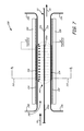
- FIGS. 5-7 illustrate an example detector 38 for use in system 10 , where detector 38 relies on capacitance sensing for measuring the powder densities of developed layers carried by belt 22 .
- Detector 38 in this embodiment is preferably positioned along belt 22 between EP engines 12 p and 12 s and layer transfusion assembly 20 , and more preferably closer to EP engines 12 p and 12 s than layer transfusion assembly 20 (e.g., as shown in FIG. 1 ).
- detector 38 includes an enclosed casing 100 having a slot 102 through which belt 22 and the developed layers 64 travel in the direction of arrow 34 .
- Casing 100 is preferably a rigid housing derived from one or more materials that minimize penetration of external magnetic fields, and further provide physical protection to its internal components.
- casing 100 preferably includes one or more magnetic shielding materials (e.g., mu-metal), which may be disposed between or laminated onto one or more rigid polymeric films.
- Casing 100 is also preferably operably secured (i.e., directly or indirectly secured) to frame 36 of system 10 to prevent detector 30 from shifting relative to belt 22 under operating vibrations from system 10 .
- casing 100 may include multiple sub-casing shells, such as upper shell 100 a and lower shell 100 b , which are preferably securable together in a detatchable manner.
- shells 100 a and 100 b are rigid and immovable relative to each other and frame 36 , allowing belt 22 to pass freely through slot 102 .
- allowing shells 100 a and 100 b to detach and separate also allows belt 22 to be readily removed from detector 38 , such as for replacement or maintenance.
- Controller assembly 40 may divide belt 22 into multiple frames along its looped length, where each frame defines an area on which a developed layer 64 is carried between EP engines 12 p and 12 s and layer transfusion assembly 20 .
- Belt 22 also includes seam 104 , which connects the opposing ends of belt 22 into the continuous loop shown above in FIG. 1 .
- detector 38 may use seam 104 as an index location along belt 22 , and identify the location of each frame along belt 22 relative to seam 104 (as well as for belt speed monitoring).
- layer 64 also includes test samples 106 p and 106 s adjacent to the layers 64 p and 64 s .
- test sample 106 p is a first bar-shaped test sample having predefined and known dimensions, and is developed by EP engine 12 p with part material 66 p .
- test sample 106 s is second a bar-shaped test sample having predefined and known dimensions, and is developed by EP engine 12 s with support material 66 s .
- Additional test samples of other materials may also be developed for each material used to print 3D part 80 and support structure 82 (e.g., a test sample may be printed for each EP engine used in system 10 ).
- test samples 106 p and 106 s assist the accuracy of the capacitance measurements by detector 38 since capacitance is dependent on the amount of material passing through an electrical field.
- the dimensions of layers 64 p and 64 s will vary depending on the bitslice geometries of 3D part 80 and support structure 82 , making it difficult to determine the powder densities or M/A values from the capacitance measurements.
- test samples 106 p and 106 s are located upstream from layers 64 p and 64 s in the rotational direction of belt 22 .
- one or both of test samples 106 p and 106 s may be located downstream from developed layer 64 .
- test sample 106 s and is depicted as being upstream from test sample 106 p the reverse order may alternatively be used.
- Controller assembly 40 may generate test samples 106 p and 106 s by modifying the bitslices used to generate layers 64 p and 64 s . For example, controller assembly 40 may add bitslice pixels for test samples 106 p and 106 s at coordinate locations that are outside the bounding boxes of layers 64 p and 64 s , but still within the usable build volume of system 10 . As can be appreciated, the number of test samples 106 p and 106 s , and the number of corresponding measurements by detector 38 per rotation of belt 22 may vary as desired.
- FIG. 6 illustrates the internal components of detector 38 .
- detector 38 also includes a plurality of sensors 108 and control board 110 , where control board 110 is illustrated schematically.
- Sensors 108 are preferably located within casing 100 , and in some embodiments, control board 110 may also be located within casing 100 .
- sensors 108 include eight capacitance sensors, individually referred to as sensors 108 a - 108 h , which are arranged as an array that is perpendicular to the movement direction of belt 22 .
- detector 38 may include fewer or more sensors 108 , such that detector 38 includes at least one sensor 108 , more preferably from two to ten sensors 108 , and even more preferably from four to eight sensors 108 .
- Sensors 108 a - 108 h are each configured to generate an electrical field that belt 22 passes through while moving in the direction of arrow 34 for measuring the capacitance of the generated electrical field.
- Belt 22 , layers 64 p and 64 s , and test samples 106 p and 106 s that pass through sensors 108 a - 108 h alter the effective capacitance of the electrical field as detected by sensors 108 a - 108 h .
- these changes in the detected capacitance may be used by controller assembly 40 to measure the powder density (and M/A values) of the test samples 106 p and 106 s.
- Sensors 108 a - 108 h may communicate with control board 110 over electrical lines 112 a - 112 h , where electrical lines 112 a - 112 h are respectively coupled to capacitance-to-digital converters (CDCs) 114 a - 114 h .
- sensors 108 a - 108 h may transmit analog capacitance signals respectively over electrical lines 112 a - 112 h
- CDCs 114 a - 114 h respectively convert these received analog capacitance signals into digital signals.
- DACs 120 and adapters 122 may each communicate with controller assembly 40 over communication line 40 a.
- DACs 12 allow detector 38 to output any desired analog signal combination from sensors 108 a - 108 h .
- adapters 122 allow detector 38 to output any desired digital signal combination from sensors 108 a - 108 h .
- controller assembly 40 may then use the analog and/or digital signals for a variety of different monitoring, calibration, and feedback controls.
- each sensor 108 preferably includes an excitation electrode 124 , a sense electrode 126 , respective support plates 128 and 130 , respective shield ground plates 132 and 134 , and respective insulating films 136 and 138 .
- Excitation electrode 124 and sense electrode 126 are a pair of electrically-conductive electrodes that are offset from each other across a gap 140 . This arrangement allows excitation electrode 124 and sense electrode 126 to function as a parallel-plate capacitor to generate an electrical field 142 across gap 140 when power is supplied to excitation electrode 124 .
- excitation electrode 124 and sense electrode 126 are preferably mounted within casing 100 in a rigid and fixed manner, such as with support plates 136 and 138 to ensure that the offset distance of gap 140 remains constant despite frame vibrations.
- Shield ground plates 132 and 134 are grounding plates respectively secured to the back sides of excitation electrode 124 and sense electrode 126 . Capacitance sensors 108 are sensitive to external electrical fields at their phase lock frequencies. As such, shield ground plates 132 and 134 guard excitation electrode 124 and sense electrode 126 from any external electrical fields by a ground connection with a low impedance path.
- the part and support materials carried by belt 22 can have spatially-varying potentials, such as up to about 400 Volts.
- insulating film 136 is preferably secured between excitation electrode 124 and belt 22
- insulating film 138 is preferably secured between sense electrode 126 and belt 22 .
- Suitable materials for insulating films 136 and 138 include polyimide films, such as polyimide tapes commercially available under the tradename “KAPTON” from E. I. du Pont de Nemours and Company, Wilmington, Del. This prevents sparks from jumping from belt 22 and/or the part and support materials to sensors 108 .
- gap 140 is preferably set as large as reasonably practical.
- suitable offset distances for gap 140 between excitation electrode 124 and sense electrode 126 range from about 0.06 inches to about 0.1 inches, and more preferably from about 0.07 inches to about 0.09 inches.
- belt 22 is positioned within gap 140 , allowing test samples 106 p and 106 s to pass through the electrical fields 142 of sensors 108 .
- the detected capacitance of electrical field 142 is affected by the thickness of belt 22 and the densities of test samples 106 p and 106 s .
- the overall dielectric constant between excitation electrode 124 and sense electrode 126 is increased by an amount that is proportional to the volume and density of the test sample 106 s.
- Equation 1 the nominal capacitance C nom value between excitation electrode 124 and sense electrode 126 may be expressed by Equation 1:
- C nom A d air ⁇ ⁇ 0 ⁇ ⁇ r , air ( Equation ⁇ ⁇ 1 )
- A is the overlapping surface area of excitation electrode 124 and sense electrode 126
- d air is air gap distance between excitation electrode 124 and sense electrode 126
- ⁇ 0 is the electric constant (i.e., about 8.85 picoFarads/meter)
- ⁇ r,air is the dielectric constant of air (i.e., about 1).
- Equation 1 provides a nominal capacitance C nom value of 660 femtoFarads.
- Equation 1 may be modified to provide a baseline capacitance C baseline value, which is the capacitance without any part or support material on belt 22 (i.e., belt 22 is in a clean state) as shown in Equation 2:
- C baseline A d air ⁇ r , air + d films ⁇ r , films + d belt ⁇ r , belt ⁇ ⁇ 0 ( Equation ⁇ ⁇ 2 )
- d air is adjusted air gap distance between excitation electrode 124 and sense electrode 126
- d films is the combined thickness of insulating films 136 and 138
- d belt is the thickness of belt 22
- ⁇ r,films is the dielectric constant of the material for insulating films 136 and 138
- ⁇ r,belt is the dielectric constant of the material for belt 22 .
- Equation 2 provides a baseline capacitance C baseline value of 736 femtoFarads.
- C sample A d air ⁇ r , air + d films ⁇ r , films + d belt ⁇ r , belt + d test ⁇ r , test ⁇ ⁇ 0 ( Equation ⁇ ⁇ 3 )
- d air is adjusted air gap distance between excitation electrode 124 and sense electrode 126
- d test is the thickness of test sample 106 p or 106 s
- ⁇ r,test is the dielectric constant of the part or support material of test sample 106 p or 106 s .
- Equation 3 provides a sample capacitance C sample value of 739 femtoFarads.
- Equation 4 provides a full-scale capacitance C f value for test sample 106 p or 106 s of about 3 femtoFarads. Accordingly, controller assembly 40 may determine the baseline capacitance C baseline from measured capacitance signals while belt 22 rotates in a clean state, may determine the sample capacitance C sample value from measured capacitance signals while belt 22 rotates with test sample 106 p or 106 s . From there, controller assembly 40 may determine the full-scale capacitance C f value as the difference between the sample capacitance C sample value and the baseline capacitance C baseline value, as shown in Equation 4.
- controller assembly 40 may then associate this full-scale capacitance C f value with a particular powder density or M/A value. Subsequently measured capacitance signals that fluctuate or drift from this full-scale capacitance C f value may then be associated with changes in the powder density or M/A value, which can detrimentally affect part strengths and accuracies.
- the noise-limited resolution of CDCs 114 sampling at 16 Hertz can achieve is about 34 attoFarads peak-to-peak, which is sufficiently signal resolution enough to detect capacitance changes from the full-scale signal C f of about 3 femtoFarads.
- test sample 106 p or 106 s will have a dwell time of 1/16 Hertz between excitation electrode 124 and sense electrode 126 . This corresponds to M/A resolutions as low as 1% with a 0.5-inch spatial resolution, where additional static capacitance from fringing and guard fields can be nulled by microprocessor 118 .
- Seam 104 of belt 22 can have a thickness that is much greater than the average thickness of belt 22 , which is detectable by detector 38 .
- seam 104 having twice the average thickness of belt 22 e.g., 0.01 inches
- detector 38 can readily recognize the location of seam 104 during every revolution of belt 22 . This allows controller assembly 40 to use seam 104 as accurately measure the rotational speed of belt 22 , as well as providing an index location for belt 22 .
- detector 38 can also map the thickness of belt 22 while belt 22 rotates in the direction of arrow 34 , and while no part or support materials are present (i.e., belt 22 is clean).
- sensors 108 a - 108 h may measure the capacitance over multiple locations along the length of belt 22 , indexed at seam 104 .
- sensors 108 a - 108 h may measure the capacitance of belt 22 over every 0.25-inch or 0.5-inch increment along the length of belt 22 , thereby providing eight lateral measurements for each longitudinal measurement. These measurements provide localized baseline capacitance C baseline values, and may then be relayed to controller assembly 40 .
- Controller assembly 40 may then create a thickness map for belt 22 that is indexed from seam 104 . During a subsequent printing operation, controller assembly 40 may then compare these localized baseline capacitance C baseline values to the sample capacitance C sample values of test samples 106 p and 106 s depending on their relative locations along (or laterally across) belt 22 . This can further increase the resolutions of the full-scale signals C f for test samples 106 p and 106 s.
- controller assembly 40 may include any suitable computer-based hardware, such as user interface 144 , memory controller 146 , processor 148 , storage media 150 , input/output (I/O) controller 152 , and communication adapter 154 . Controller assembly 40 may also include a variety of additional components that are contained in conventional computers, servers, media devices, and/or printer controllers.
- User interface 144 is a user-operated interface (e.g., keyboards, touch pads, touch-screen displays, display monitors, and other eye, voice, movement, or hand-operated controls) configured to operate controller assembly 40 .
- Memory controller 146 is a circuit assembly that interfaces the components of controller assembly 40 with one or more volatile random access memory (RAM) modules of storage media 150 .
- Processor 148 is one or more computer-processing units configured to operate controller assembly 40 , optionally with memory controller 146 .
- processor 148 may include one or more microprocessor-based engine control systems and/or digitally-controlled raster imaging processor systems.
- Storage media 150 is one or more internal and/or external data storage devices or computer storage media for controller assembly 40 , such as volatile RAM modules, read-only memory modules, optical media, magnetic media (e.g., hard disc drives), solid-state media (e.g., FLASH memory and solid-state drives), analog media, and the like.
- Storage media 150 may retain an executable copy of processing program 156 , one or more digital models 158 to be printed with system 10 , and generated bitslices 160 , each which may be utilized as disclosed in co-filed U.S. patent application Ser. No. 14/218,084,entitled “Additive Manufacturing With Virtual Planarization Control”.
- I/O controller 152 is a circuit assembly that interfaces memory controller 146 , processor 148 , and storage media 150 with various input and output components of controller assembly 40 , including communication adapter 154 .
- Communication adapter 154 is one or more wired or wireless transmitter/receiver adapters configured to communicate over communication lines 40 a and 40 b.
- Controller assembly 40 may receive signals of the sample capacitance C sample values from detector 38 over communication line 40 a , such as from DACs 120 and/or adapters 122 of detector 38 , and store the received signals on storage media 150 as capacitance signal data 162 .
- controller assembly 40 preferably includes one or more analog-to-digital converters (not shown) to digitized the received analog signals for storage on storage media 150 and/or subsequent processing.
- controller assembly 40 may also create a thickness map for belt 22 from the localized baseline capacitance C baseline values, and which are indexed from seam 104 . For instance, at the start up of a printing operation, controller assembly 40 may rotate belt 22 in the direction of arrow 34 , and have detector 38 collect the localized baseline capacitance C baseline values prior to EP engines 12 p and 12 s operating. These localized baseline capacitance C baseline values may then be transmitted to controller assembly 40 and stored on storage media 150 as an initial belt map 164 , which functions as the capacitance baseline for the localized points along belt 22 , pursuant to Equation 2 shown above.
- frame 36 can heat up due to the heating steps at layer transfusion assembly 20 . Because of this temperature increase, the distance of gap 140 between excitation electrode 124 and sense electrode 126 can potentially increase, such as due to material expansions in casing 100 . In fact, if the temperature increase is significant, gap 140 can swell by as much as 50% of the thickness of test samples 106 a and 106 b.
- controller assembly 40 preferably introduces one or more EP engine pauses to allow a clean belt 22 to rotate one or more full cycles past detector 38 , as indexed by seam 104 .
- detector 38 may measure clean regions of belt 22 between the developed layers 64 to generate a liner dilation if the average baseline capacitance C baseline values deviate significantly from the values in initial belt map 164 .
- controller assembly 40 may skip a particular frame location along belt 22 during each revolution to allow detector 38 to measure the clean belt 22 of the skipped frame location. The skipped frame location may then shift to the next adjacent frame location during the subsequent revolution, and so on.
- these new localized baseline capacitance C baseline values may then be transmitted to controller assembly 40 and stored on storage media 150 as updated belt map 166 , which may replace the values of initial belt map 164 as the capacitance baseline. Furthermore, these updates may be made periodically through the printing operation to maintain good signal-to-noise resolutions, and for system performance monitoring.
- the capacitance signal data 162 may be used to measure the powder densities of the part and support materials 66 p and 66 during printing operations, where capacitance signal fluctuations or drifts from the full-scale signals C f may identify powder density changes. If the measured capacitance signals increase, this can correspond to a decrease in powder density, and vice versa.
- These powder density or M/A values may be used for a variety of purposes, such as performance monitoring, calibration, and feedback controls.
- the measured powder densities may be used to modify the Q/M ratios of part material 66 p and/or support material 66 s to account for powder-density drifts over time. This can assist in stabilizing the powder densities of these materials.
- controller assembly 40 may also generate reports for the processing parameters of system 10 , including the capacitance signal data 162 , and the associated powder density or M/A values. This can assist with any potential processing or maintenance issues with system 10 .
- controller assembly 40 may also utilize the measured z-heights in combination with the measure M/A values from detector 38 . This combined information can then be used to increase the strengths and qualities of 3D part 80 and support structure 82 , such as by calibration and/or real-time feedback control.
- controller assembly 168 may also imager LED data 168 , such as imaging on-time values for the LEDs, where imager data 168 may be stored on storage media 150 .
- imager 56 may include an LED array 170 having a plurality of individual LEDs 172 , and optionally additional optics 174 .
- controller assembly 40 directs LED array 170 selectively illuminate the individual LEDs 172 with preset on-time durations, based on bitslices 160 . This emits electromagnetic radiation toward the uniform electrostatic charge on surface 46 as surface 46 rotates in the direction of arrow 52 past imager 56 .
- the preset on-time durations affect the intensities of the charge patterns on surface 46 , which correspondingly affects how much of part material 66 p or support material 66 s is attracted to surface 46 , based on the Q/M of the given material.
- the preset on-time durations of LEDs 172 affect the powder densities of the part material 66 p and support material 66 s that are formed on surface 46 to produce layers 64 p and 64 s (and test samples 106 p and 106 s ).
- controller assembly 40 may modify imager data 168 of the on-time registers for LEDs 172 to assist in stabilizing the powder densities in the developed layers 64 p and 64 s . These modifications may be performed on a global scale, where the on-time duration for each LED 172 in LED array 170 may be modified by the same amount, such as to compensate for powder density drifts over time.
- the LEDs 172 in LED array 170 may be grouped into blocks 176 , such as blocks 176 a - 176 h , each of which may correspond to one of the sensors 108 of detector 38 (or to multiple sensors 108 ).
- each block 176 a - 176 h may be associated with one or more corresponding sensors 108 a - 108 h , allowing controller assembly 40 to use each sensor 108 to modify the on-time duration for each LED 172 in the associated block 176 by the same amount. This can also compensate for powder density drifts over time, and provides greater control over LEDs 172 compared to the global modification to LED array 170 .
- controller assembly 40 may modify imager data 168 of the on-time registers for each individual LED 172 in LED array 170 . This can provide high-resolution control over each individual LED 172 to compensate for a variety of powder density deviations.
- controller assembly 40 may modify the on-time durations for LEDs 172 during calibration routines, such as between printing operations and/or during the start of a printing operation. Additionally, controller assembly 40 may modify the on-time durations for LEDs 172 during a printing operation, such as with feedback control loops. This can assist in compensate for fluctuations or drifts in the powder densities, allowing real-time control over processing variations in system 10 .
Abstract
Description
where A is the overlapping surface area of
where dair is adjusted air gap distance between
where dair is adjusted air gap distance between
C f =C sample −C baseline (Equation 4)
Claims (19)
Priority Applications (3)
| Application Number | Priority Date | Filing Date | Title |
|---|---|---|---|
| US14/218,114 US9643357B2 (en) | 2014-03-18 | 2014-03-18 | Electrophotography-based additive manufacturing with powder density detection and utilization |
| PCT/US2015/017978 WO2015142494A1 (en) | 2014-03-18 | 2015-02-27 | Eletrophotography-based additive manufacturing with powder density detection and utilization |
| EP15709060.6A EP3120196B1 (en) | 2014-03-18 | 2015-02-27 | Electrophotography-based additive manufacturing with powder density detection and utilization |
Applications Claiming Priority (1)
| Application Number | Priority Date | Filing Date | Title |
|---|---|---|---|
| US14/218,114 US9643357B2 (en) | 2014-03-18 | 2014-03-18 | Electrophotography-based additive manufacturing with powder density detection and utilization |
Publications (2)
| Publication Number | Publication Date |
|---|---|
| US20150266236A1 US20150266236A1 (en) | 2015-09-24 |
| US9643357B2 true US9643357B2 (en) | 2017-05-09 |
Family
ID=52633716
Family Applications (1)
| Application Number | Title | Priority Date | Filing Date |
|---|---|---|---|
| US14/218,114 Active 2035-05-09 US9643357B2 (en) | 2014-03-18 | 2014-03-18 | Electrophotography-based additive manufacturing with powder density detection and utilization |
Country Status (3)
| Country | Link |
|---|---|
| US (1) | US9643357B2 (en) |
| EP (1) | EP3120196B1 (en) |
| WO (1) | WO2015142494A1 (en) |
Cited By (5)
| Publication number | Priority date | Publication date | Assignee | Title |
|---|---|---|---|---|
| US20170138906A1 (en) * | 2015-11-13 | 2017-05-18 | Honeywell Fed Mfg & Tech Llc | System and method for inspecting parts using frequency response function |
| US20230158616A1 (en) * | 2015-10-30 | 2023-05-25 | Seurat Technologies, Inc. | Multi-Functional Ingester System For Additive Manufacturing |
| US11660808B2 (en) | 2018-07-26 | 2023-05-30 | Hewlett-Packard Development Company, L.P. | Cleaning mechanisms for build material level sensors |
| US11660817B2 (en) | 2017-11-10 | 2023-05-30 | General Electric Company | Methods for removing loose particles from an object built by additive manufacturing |
| US11865613B2 (en) | 2021-10-07 | 2024-01-09 | Additive Monitoring Systems, Llc | Structured light part quality monitoring for additive manufacturing and methods of use |
Families Citing this family (16)
| Publication number | Priority date | Publication date | Assignee | Title |
|---|---|---|---|---|
| US8888480B2 (en) | 2012-09-05 | 2014-11-18 | Aprecia Pharmaceuticals Company | Three-dimensional printing system and equipment assembly |
| US9643251B2 (en) * | 2014-06-13 | 2017-05-09 | Zin Technologies, Inc. | Optimized additive manufacturing process |
| EP3337624A4 (en) | 2015-08-21 | 2019-10-30 | Aprecia Pharmaceuticals LLC | Three-dimensional printing system and equipment assembly |
| US10967462B2 (en) * | 2015-12-08 | 2021-04-06 | Honeywell Federal Manufacturing & Technologies, Llc | Foil deposition onto an additive manufactured substrate |
| US10814391B2 (en) | 2016-09-13 | 2020-10-27 | General Electric Company | Additive manufacturing material analysis system and related method |
| GB2560310A (en) * | 2017-03-03 | 2018-09-12 | Mcor Tech Limited | 3D printer and 3D printing method |
| GB2564710A (en) * | 2017-07-21 | 2019-01-23 | Lpw Technology Ltd | Measuring density of a powder bed and detecting a defect in an additively manufactured article |
| EP3693103B1 (en) * | 2017-10-06 | 2023-04-26 | IHI Corporation | Powder supply device and additive manufacturing device |
| US11458687B2 (en) | 2018-04-24 | 2022-10-04 | Hewlett-Packard Development Company, L.P. | Additive manufacturing system |
| US11203156B2 (en) | 2018-08-20 | 2021-12-21 | NEXA3D Inc. | Methods and systems for photo-curing photo-sensitive material for printing and other applications |
| US20200079025A1 (en) * | 2018-09-06 | 2020-03-12 | Evolve Additive Solutions, Inc. | Transfuse roller tracking in selective layer deposition based additive manufacturing |
| KR20210090197A (en) | 2018-11-09 | 2021-07-19 | 넥사3디 인코포레이티드 | 3D Printing System |
| JP2022525761A (en) | 2019-03-18 | 2022-05-19 | ネクサ3ディー インコーポレイテッド | Adduct manufacturing method and system |
| US10967573B2 (en) | 2019-04-02 | 2021-04-06 | NEXA3D Inc. | Tank assembly and components thereof for a 3D printing system |
| CN115195123B (en) * | 2022-06-06 | 2024-01-05 | 深圳市纵维立方科技有限公司 | 3D printing failure detection method, 3D printer and storage medium |
| JP2023182461A (en) * | 2022-06-14 | 2023-12-26 | 富士フイルムビジネスイノベーション株式会社 | Endless belt, transfer device and image formation apparatus |
Citations (94)
| Publication number | Priority date | Publication date | Assignee | Title |
|---|---|---|---|---|
| US2297691A (en) | 1939-04-04 | 1942-10-06 | Chester F Carlson | Electrophotography |
| US3247455A (en) * | 1962-03-29 | 1966-04-19 | Forte Engineering Corp | Apparatus for measurement of capacitivity of materials in large bulk form having movable support and guide means |
| US4752727A (en) * | 1984-09-10 | 1988-06-21 | Endress U. Hauser Gmbh U. Co. | Arrangement for detecting spatial inhomogeneities in a dielectric |
| US4988602A (en) | 1990-04-18 | 1991-01-29 | Minnesota Mining And Manufacturing Co. | Liquid electrophotographic toner with acid containing polyester resins |
| US5088047A (en) | 1989-10-16 | 1992-02-11 | Bynum David K | Automated manufacturing system using thin sections |
| US5099288A (en) | 1990-11-19 | 1992-03-24 | Lexmark International, Inc. | Fixing device with selectable finish |
| JPH05165350A (en) | 1991-12-17 | 1993-07-02 | Konica Corp | Fixing device |
| US5254421A (en) | 1989-06-28 | 1993-10-19 | Agfa-Gevaert, N.V. | Toner receiving printing plate |
| US5354799A (en) | 1992-11-16 | 1994-10-11 | Eastman Kodak Company | Limited coalescence process |
| US5354414A (en) | 1988-10-05 | 1994-10-11 | Michael Feygin | Apparatus and method for forming an integral object from laminations |
| US5514232A (en) | 1993-11-24 | 1996-05-07 | Burns; Marshall | Method and apparatus for automatic fabrication of three-dimensional objects |
| EP0712051A2 (en) | 1994-11-09 | 1996-05-15 | Texas Instruments Incorporated | Improvements in or relating to the manufacture of three-dimensional objects |
| JPH08281808A (en) | 1995-04-17 | 1996-10-29 | Ricoh Co Ltd | Manufacture of stereoscopic shape |
| US5592266A (en) | 1994-09-08 | 1997-01-07 | Samsung Electronics Co., Ltd. | Electrophotographic process cartridge |
| US5593531A (en) | 1994-11-09 | 1997-01-14 | Texas Instruments Incorporated | System, method and process for fabrication of 3-dimensional objects by a static electrostatic imaging and lamination device |
| US5594652A (en) | 1991-01-31 | 1997-01-14 | Texas Instruments Incorporated | Method and apparatus for the computer-controlled manufacture of three-dimensional objects from computer data |
| US5764521A (en) | 1995-11-13 | 1998-06-09 | Stratasys Inc. | Method and apparatus for solid prototyping |
| WO1998051464A1 (en) | 1997-04-30 | 1998-11-19 | Ralf Larsson | Method and device for manufacturing three-dimensional bodies |
| US5866058A (en) | 1997-05-29 | 1999-02-02 | Stratasys Inc. | Method for rapid prototyping of solid models |
| US5981616A (en) | 1996-12-13 | 1999-11-09 | Dsm N.V. | Photo-curable resin composition used for photo fabication of three-dimensional objects |
| US5990268A (en) | 1992-11-23 | 1999-11-23 | Dtm Corporation | Sinterable semi-crystalline powder and near-fully dense article formed therewith |
| US6052551A (en) | 1997-04-07 | 2000-04-18 | Xeikon N.V. | Electrostatographic printer and method |
| US6066285A (en) | 1997-12-12 | 2000-05-23 | University Of Florida | Solid freeform fabrication using power deposition |
| US6085957A (en) | 1996-04-08 | 2000-07-11 | Stratasys, Inc. | Volumetric feed control for flexible filament |
| US6169605B1 (en) | 1991-01-31 | 2001-01-02 | Texas Instruments Incorporated | Method and apparatus for the computer-controlled manufacture of three-dimensional objects from computer data |
| JP2001075376A (en) | 1999-09-06 | 2001-03-23 | Canon Inc | Image forming device |
| US6206672B1 (en) * | 1994-03-31 | 2001-03-27 | Edward P. Grenda | Apparatus of fabricating 3 dimensional objects by means of electrophotography, ionography or a similar process |
| US6329115B1 (en) | 1996-09-11 | 2001-12-11 | Ricoh Company, Ltd. | Toner for use in electrophotography and method of producing the same |
| US20020014116A1 (en) * | 1999-02-26 | 2002-02-07 | Campbell Ronald H. | Methods and systems for measuring crop density |
| US6376148B1 (en) | 2001-01-17 | 2002-04-23 | Nanotek Instruments, Inc. | Layer manufacturing using electrostatic imaging and lamination |
| US20020093115A1 (en) | 2001-01-12 | 2002-07-18 | Jang B. Z. | Layer manufacturing method and apparatus using a programmable planar light source |
| US20020145213A1 (en) | 2001-04-10 | 2002-10-10 | Junhai Liu | Layer manufacturing of a multi-material or multi-color 3-D object using electrostatic imaging and lamination |
| JP2002347129A (en) | 2001-05-25 | 2002-12-04 | Konica Corp | Apparatus and method for three-dimensional shaping |
| US6492651B2 (en) | 2001-02-08 | 2002-12-10 | 3D Systems, Inc. | Surface scanning system for selective deposition modeling |
| US6509128B1 (en) | 2000-10-25 | 2003-01-21 | 3M Innovative Properties Company | Imagewise printing of adhesives and limited coalescence polymerization method |
| JP2003053849A (en) | 2001-08-16 | 2003-02-26 | Konica Corp | Laminate shaping apparatus and laminate shaping method |
| JP2003071940A (en) | 2001-09-03 | 2003-03-12 | Konica Corp | Apparatus for lamination shaping and method for lamination shaping |
| US20030087176A1 (en) | 2001-07-25 | 2003-05-08 | Ezenyilimba Matthew C. | Chemically prepared toners of controlled particle shape |
| US20040173946A1 (en) | 2003-03-07 | 2004-09-09 | Rolf Pfeifer | Process for quality control for a powder based layer building up process |
| US6799959B1 (en) | 1999-09-14 | 2004-10-05 | Minolta Co., Ltd. | Apparatus for forming a three-dimensional product |
| US6815636B2 (en) | 2003-04-09 | 2004-11-09 | 3D Systems, Inc. | Sintering using thermal image feedback |
| US20040232583A1 (en) | 2003-03-15 | 2004-11-25 | Degusa Ag | Process for producing three-dimensional objects by means of microwave radiation |
| JP2005062860A (en) | 2003-07-31 | 2005-03-10 | Tokai Rubber Ind Ltd | Manufacturing process for electrophotographic endless belt |
| US6887640B2 (en) | 2002-02-28 | 2005-05-03 | Sukun Zhang | Energy activated electrographic printing process |
| US20050207801A1 (en) | 2004-03-18 | 2005-09-22 | Hiroyuki Kunii | Method of uniformly fixing toner to recording medium in image forming apparatus |
| US20050218549A1 (en) | 2004-04-02 | 2005-10-06 | Isaac Farr | Solid freeform compositions, methods of application thereof, and systems for use thereof |
| US7011783B2 (en) | 2001-10-24 | 2006-03-14 | 3D Systems, Inc. | Cooling techniques in solid freeform fabrication |
| JP2006182813A (en) | 2004-12-24 | 2006-07-13 | Sumitomo Rubber Ind Ltd | Electroconductive seamless belt, manufacturing method of electroconductive seamless belt, and image-forming apparatus equipped with electroconductive seamless belt |
| US7077638B2 (en) | 1995-09-27 | 2006-07-18 | 3D Systems, Inc. | Selective deposition modeling method and apparatus for forming three-dimensional objects and supports |
| US7208257B2 (en) | 2004-06-25 | 2007-04-24 | Xerox Corporation | Electron beam curable toners and processes thereof |
| US7261542B2 (en) | 2004-03-18 | 2007-08-28 | Desktop Factory, Inc. | Apparatus for three dimensional printing using image layers |
| WO2007114895A2 (en) | 2006-04-06 | 2007-10-11 | Z Corporation | Production of three-dimensional objects by use of electromagnetic radiation |
| US7291242B2 (en) | 2002-12-20 | 2007-11-06 | University Of Southern California | Methods for reduction of powder waste in selective inhibition of sintering (SIS) |
| US20080032083A1 (en) | 2004-05-12 | 2008-02-07 | Massachusetts Institute Of Technology | Manufacturing Process, Such as Three-Dimensional Printing, Including Solvent Vapor Filming and the Like |
| US20080169589A1 (en) | 2007-01-17 | 2008-07-17 | Sperry Charles R | Solid imaging apparatus and method |
| US20080171284A1 (en) | 2007-01-17 | 2008-07-17 | Hull Charles W | Method for Removing Excess Uncured Build Material in Solid Imaging |
| US20080169585A1 (en) | 2007-01-12 | 2008-07-17 | Stratasys, Inc. | Surface-treatment method for rapid-manufactured three-dimensional objects |
| GB2446386A (en) | 2007-02-06 | 2008-08-13 | Univ Montfort | Electrostatic printing method and its use in rapid prototyping |
| US20080226346A1 (en) | 2007-01-17 | 2008-09-18 | 3D Systems, Inc. | Inkjet Solid Imaging System and Method for Solid Imaging |
| CN101310964A (en) | 2008-07-10 | 2008-11-26 | 华南理工大学 | Precinct laser fusion rapid molding method and device of medical implantation material wax mould |
| US20090236775A1 (en) | 2008-03-19 | 2009-09-24 | Evonik Degussa Gmbh | Copolyamide powder and its preparation, use of copolyamide powder in a shaping process and mouldings produced from this copolyamide powder |
| US20110117485A1 (en) | 2007-08-27 | 2011-05-19 | Sintermask Gmbh | Toner composition, developer comprising the toner composition, and method in connection with the production of a volume body |
| WO2011065920A1 (en) | 2009-11-26 | 2011-06-03 | Yu En Tan | Process for building three-dimensional objects |
| US7988906B2 (en) | 2005-07-16 | 2011-08-02 | Evonik Degussa Gmbh | Three-dimensional layer-by-layer production process with powders based on cyclic oligomers |
| US20110190446A1 (en) | 2010-02-02 | 2011-08-04 | Sony Corporation | Three-dimensional modeling apparatus, method of manufacturing a three-dimensional object, and three-dimensional object |
| US20110186081A1 (en) | 2010-01-05 | 2011-08-04 | Stratasys, Inc. | Support cleaning system |
| US20110222884A1 (en) | 2010-03-09 | 2011-09-15 | Konica Minolta Business Technologies, Inc. | Deposited toner measuring apparatus, image formation apparatus, and method for controlling image formation apparatus |
| US20120041132A1 (en) | 2004-04-27 | 2012-02-16 | Evonik Degussa Gmbh | Polymer powder comprising polyamide use thereof in a moulding method and moulded body made from said polymer powder |
| US8119053B1 (en) | 2004-03-18 | 2012-02-21 | 3D Systems, Inc. | Apparatus for three dimensional printing using imaged layers |
| US8123999B2 (en) | 2002-04-17 | 2012-02-28 | Stratasys, Inc. | Smoothing method for layered deposition modeling |
| US8124192B2 (en) | 2007-06-25 | 2012-02-28 | Eos Gmbh Electro Optical Systems | Layer application device for an electrostatic layer application of a building material in powder form and device and method for manufacturing a three-dimensional object |
| WO2012034666A1 (en) | 2010-09-17 | 2012-03-22 | Fraunhofer-Gesellschaft zur Förderung der angewandten Forschung e.V. | Polymer particles and method for producing a three-dimensional structure therefrom by means of an electrographic method |
| US8147910B2 (en) | 2009-02-24 | 2012-04-03 | Objet Ltd. | Method and apparatus for three-dimensional printing |
| US8173258B2 (en) | 2004-10-01 | 2012-05-08 | Evonik Degussa Gmbh | Powder with improved recycling properties, process for its production, and use of the powder in a process for producing three-dimensional objects |
| US20120139167A1 (en) | 2009-08-18 | 2012-06-07 | Sintermask Gmbh | Method and device for producing a three-dimensional object |
| US8216757B2 (en) | 2007-12-17 | 2012-07-10 | Fuji Xerox Co., Ltd. | Toner for electrostatic charge image development and manufacturing method thereof, and electrostatic charge image developer, toner cartridge, process cartridge and image forming apparatus |
| US8221671B2 (en) | 2007-01-17 | 2012-07-17 | 3D Systems, Inc. | Imager and method for consistent repeatable alignment in a solid imaging apparatus |
| US8222908B2 (en) | 2010-02-16 | 2012-07-17 | Stratasys, Inc. | Capacitive detector for use in extrusion-based digital manufacturing systems |
| US20120201960A1 (en) | 2009-10-13 | 2012-08-09 | Blueprinter Aps | Three-dimensional printer |
| US20120202012A1 (en) | 2011-02-03 | 2012-08-09 | Evonik Degussa Gmbh | Process for the production of a three dimensional system |
| US8249480B2 (en) | 2009-06-25 | 2012-08-21 | Eastman Kodak Company | Fusing apparatus for high speed electrophotography system |
| US8246888B2 (en) | 2008-10-17 | 2012-08-21 | Stratasys, Inc. | Support material for digital manufacturing systems |
| US20120237870A1 (en) | 2011-03-16 | 2012-09-20 | Masaki Watanabe | Toner, method of manufacturing toner, image forming method, image forming apparatus, and process cartridge |
| US20120274002A1 (en) | 2011-04-27 | 2012-11-01 | Canon Kabushiki Kaisha | Method for manufacturing seamless belt for electrophotography |
| JP5165350B2 (en) | 2007-01-26 | 2013-03-21 | 三菱樹脂株式会社 | Polyester heat shrinkable film roll |
| US20130077997A1 (en) | 2011-09-23 | 2013-03-28 | Stratasys, Inc. | Electrophotography-based additive manufacturing system with transfer-medium service loops |
| US20130077996A1 (en) | 2011-09-23 | 2013-03-28 | Stratasys, Inc. | Electrophotography-based additive manufacturing system with reciprocating operation |
| US20130078013A1 (en) * | 2011-09-23 | 2013-03-28 | Stratasys, Inc. | Layer Transfusion with Part Heating for Additive Manufacturing |
| US8459280B2 (en) | 2011-09-23 | 2013-06-11 | Stratasys, Inc. | Support structure removal system |
| US20130186549A1 (en) | 2011-09-23 | 2013-07-25 | Stratasys, Inc. | Layer transfusion for additive manufacturing |
| US20130186558A1 (en) | 2011-09-23 | 2013-07-25 | Stratasys, Inc. | Layer transfusion with heat capacitor belt for additive manufacturing |
| US20140004462A1 (en) | 2012-06-29 | 2014-01-02 | Mark Cameron Zaretsky | Making article with desired profile |
| US20140167326A1 (en) | 2011-05-31 | 2014-06-19 | University Of Warwick | Additive building |
| US20160161872A1 (en) * | 2013-07-17 | 2016-06-09 | Stratasys, Inc. | Semi-crystalline consumable materials for electrophotography-based additive manufacturing system |
-
2014
- 2014-03-18 US US14/218,114 patent/US9643357B2/en active Active
-
2015
- 2015-02-27 WO PCT/US2015/017978 patent/WO2015142494A1/en active Application Filing
- 2015-02-27 EP EP15709060.6A patent/EP3120196B1/en active Active
Patent Citations (103)
| Publication number | Priority date | Publication date | Assignee | Title |
|---|---|---|---|---|
| US2297691A (en) | 1939-04-04 | 1942-10-06 | Chester F Carlson | Electrophotography |
| US3247455A (en) * | 1962-03-29 | 1966-04-19 | Forte Engineering Corp | Apparatus for measurement of capacitivity of materials in large bulk form having movable support and guide means |
| US4752727A (en) * | 1984-09-10 | 1988-06-21 | Endress U. Hauser Gmbh U. Co. | Arrangement for detecting spatial inhomogeneities in a dielectric |
| US5354414A (en) | 1988-10-05 | 1994-10-11 | Michael Feygin | Apparatus and method for forming an integral object from laminations |
| US5254421A (en) | 1989-06-28 | 1993-10-19 | Agfa-Gevaert, N.V. | Toner receiving printing plate |
| US5088047A (en) | 1989-10-16 | 1992-02-11 | Bynum David K | Automated manufacturing system using thin sections |
| US4988602A (en) | 1990-04-18 | 1991-01-29 | Minnesota Mining And Manufacturing Co. | Liquid electrophotographic toner with acid containing polyester resins |
| US5099288A (en) | 1990-11-19 | 1992-03-24 | Lexmark International, Inc. | Fixing device with selectable finish |
| US5594652A (en) | 1991-01-31 | 1997-01-14 | Texas Instruments Incorporated | Method and apparatus for the computer-controlled manufacture of three-dimensional objects from computer data |
| US6169605B1 (en) | 1991-01-31 | 2001-01-02 | Texas Instruments Incorporated | Method and apparatus for the computer-controlled manufacture of three-dimensional objects from computer data |
| JPH05165350A (en) | 1991-12-17 | 1993-07-02 | Konica Corp | Fixing device |
| US5354799A (en) | 1992-11-16 | 1994-10-11 | Eastman Kodak Company | Limited coalescence process |
| US5990268A (en) | 1992-11-23 | 1999-11-23 | Dtm Corporation | Sinterable semi-crystalline powder and near-fully dense article formed therewith |
| US5514232A (en) | 1993-11-24 | 1996-05-07 | Burns; Marshall | Method and apparatus for automatic fabrication of three-dimensional objects |
| US6206672B1 (en) * | 1994-03-31 | 2001-03-27 | Edward P. Grenda | Apparatus of fabricating 3 dimensional objects by means of electrophotography, ionography or a similar process |
| US5592266A (en) | 1994-09-08 | 1997-01-07 | Samsung Electronics Co., Ltd. | Electrophotographic process cartridge |
| EP0712051A2 (en) | 1994-11-09 | 1996-05-15 | Texas Instruments Incorporated | Improvements in or relating to the manufacture of three-dimensional objects |
| US5593531A (en) | 1994-11-09 | 1997-01-14 | Texas Instruments Incorporated | System, method and process for fabrication of 3-dimensional objects by a static electrostatic imaging and lamination device |
| JPH08281808A (en) | 1995-04-17 | 1996-10-29 | Ricoh Co Ltd | Manufacture of stereoscopic shape |
| US7077638B2 (en) | 1995-09-27 | 2006-07-18 | 3D Systems, Inc. | Selective deposition modeling method and apparatus for forming three-dimensional objects and supports |
| US5764521A (en) | 1995-11-13 | 1998-06-09 | Stratasys Inc. | Method and apparatus for solid prototyping |
| US6085957A (en) | 1996-04-08 | 2000-07-11 | Stratasys, Inc. | Volumetric feed control for flexible filament |
| US6329115B1 (en) | 1996-09-11 | 2001-12-11 | Ricoh Company, Ltd. | Toner for use in electrophotography and method of producing the same |
| US5981616A (en) | 1996-12-13 | 1999-11-09 | Dsm N.V. | Photo-curable resin composition used for photo fabication of three-dimensional objects |
| US6052551A (en) | 1997-04-07 | 2000-04-18 | Xeikon N.V. | Electrostatographic printer and method |
| WO1998051464A1 (en) | 1997-04-30 | 1998-11-19 | Ralf Larsson | Method and device for manufacturing three-dimensional bodies |
| US6531086B1 (en) | 1997-04-30 | 2003-03-11 | Speed Part Rp Ab | Method and device for manufacturing three-dimensional bodies |
| US5866058A (en) | 1997-05-29 | 1999-02-02 | Stratasys Inc. | Method for rapid prototyping of solid models |
| US6066285A (en) | 1997-12-12 | 2000-05-23 | University Of Florida | Solid freeform fabrication using power deposition |
| US20020014116A1 (en) * | 1999-02-26 | 2002-02-07 | Campbell Ronald H. | Methods and systems for measuring crop density |
| JP2001075376A (en) | 1999-09-06 | 2001-03-23 | Canon Inc | Image forming device |
| US6799959B1 (en) | 1999-09-14 | 2004-10-05 | Minolta Co., Ltd. | Apparatus for forming a three-dimensional product |
| US6509128B1 (en) | 2000-10-25 | 2003-01-21 | 3M Innovative Properties Company | Imagewise printing of adhesives and limited coalescence polymerization method |
| US20020093115A1 (en) | 2001-01-12 | 2002-07-18 | Jang B. Z. | Layer manufacturing method and apparatus using a programmable planar light source |
| US6376148B1 (en) | 2001-01-17 | 2002-04-23 | Nanotek Instruments, Inc. | Layer manufacturing using electrostatic imaging and lamination |
| US6492651B2 (en) | 2001-02-08 | 2002-12-10 | 3D Systems, Inc. | Surface scanning system for selective deposition modeling |
| US20020145213A1 (en) | 2001-04-10 | 2002-10-10 | Junhai Liu | Layer manufacturing of a multi-material or multi-color 3-D object using electrostatic imaging and lamination |
| US6780368B2 (en) | 2001-04-10 | 2004-08-24 | Nanotek Instruments, Inc. | Layer manufacturing of a multi-material or multi-color 3-D object using electrostatic imaging and lamination |
| JP2002347129A (en) | 2001-05-25 | 2002-12-04 | Konica Corp | Apparatus and method for three-dimensional shaping |
| US20030087176A1 (en) | 2001-07-25 | 2003-05-08 | Ezenyilimba Matthew C. | Chemically prepared toners of controlled particle shape |
| JP2003053849A (en) | 2001-08-16 | 2003-02-26 | Konica Corp | Laminate shaping apparatus and laminate shaping method |
| JP2003071940A (en) | 2001-09-03 | 2003-03-12 | Konica Corp | Apparatus for lamination shaping and method for lamination shaping |
| US7011783B2 (en) | 2001-10-24 | 2006-03-14 | 3D Systems, Inc. | Cooling techniques in solid freeform fabrication |
| US7261541B2 (en) | 2001-10-24 | 2007-08-28 | 3D Systems, Inc. | Cooling techniques in solid freeform fabrication |
| US6887640B2 (en) | 2002-02-28 | 2005-05-03 | Sukun Zhang | Energy activated electrographic printing process |
| US8123999B2 (en) | 2002-04-17 | 2012-02-28 | Stratasys, Inc. | Smoothing method for layered deposition modeling |
| US8047251B2 (en) | 2002-12-20 | 2011-11-01 | University Of Southern California | Reduction of powder waste in selective inhibition of sintering |
| US7291242B2 (en) | 2002-12-20 | 2007-11-06 | University Of Southern California | Methods for reduction of powder waste in selective inhibition of sintering (SIS) |
| US20040173946A1 (en) | 2003-03-07 | 2004-09-09 | Rolf Pfeifer | Process for quality control for a powder based layer building up process |
| US20040232583A1 (en) | 2003-03-15 | 2004-11-25 | Degusa Ag | Process for producing three-dimensional objects by means of microwave radiation |
| US6815636B2 (en) | 2003-04-09 | 2004-11-09 | 3D Systems, Inc. | Sintering using thermal image feedback |
| JP2005062860A (en) | 2003-07-31 | 2005-03-10 | Tokai Rubber Ind Ltd | Manufacturing process for electrophotographic endless belt |
| US8119053B1 (en) | 2004-03-18 | 2012-02-21 | 3D Systems, Inc. | Apparatus for three dimensional printing using imaged layers |
| US20050207801A1 (en) | 2004-03-18 | 2005-09-22 | Hiroyuki Kunii | Method of uniformly fixing toner to recording medium in image forming apparatus |
| US7261542B2 (en) | 2004-03-18 | 2007-08-28 | Desktop Factory, Inc. | Apparatus for three dimensional printing using image layers |
| US20050218549A1 (en) | 2004-04-02 | 2005-10-06 | Isaac Farr | Solid freeform compositions, methods of application thereof, and systems for use thereof |
| US7435763B2 (en) | 2004-04-02 | 2008-10-14 | Hewlett-Packard Development Company, L.P. | Solid freeform compositions, methods of application thereof, and systems for use thereof |
| US20120041132A1 (en) | 2004-04-27 | 2012-02-16 | Evonik Degussa Gmbh | Polymer powder comprising polyamide use thereof in a moulding method and moulded body made from said polymer powder |
| US7815826B2 (en) | 2004-05-12 | 2010-10-19 | Massachusetts Institute Of Technology | Manufacturing process, such as three-dimensional printing, including solvent vapor filming and the like |
| US20080032083A1 (en) | 2004-05-12 | 2008-02-07 | Massachusetts Institute Of Technology | Manufacturing Process, Such as Three-Dimensional Printing, Including Solvent Vapor Filming and the Like |
| US7208257B2 (en) | 2004-06-25 | 2007-04-24 | Xerox Corporation | Electron beam curable toners and processes thereof |
| US8173258B2 (en) | 2004-10-01 | 2012-05-08 | Evonik Degussa Gmbh | Powder with improved recycling properties, process for its production, and use of the powder in a process for producing three-dimensional objects |
| JP2006182813A (en) | 2004-12-24 | 2006-07-13 | Sumitomo Rubber Ind Ltd | Electroconductive seamless belt, manufacturing method of electroconductive seamless belt, and image-forming apparatus equipped with electroconductive seamless belt |
| US7988906B2 (en) | 2005-07-16 | 2011-08-02 | Evonik Degussa Gmbh | Three-dimensional layer-by-layer production process with powders based on cyclic oligomers |
| WO2007114895A2 (en) | 2006-04-06 | 2007-10-11 | Z Corporation | Production of three-dimensional objects by use of electromagnetic radiation |
| US20080169585A1 (en) | 2007-01-12 | 2008-07-17 | Stratasys, Inc. | Surface-treatment method for rapid-manufactured three-dimensional objects |
| US8221671B2 (en) | 2007-01-17 | 2012-07-17 | 3D Systems, Inc. | Imager and method for consistent repeatable alignment in a solid imaging apparatus |
| US20080226346A1 (en) | 2007-01-17 | 2008-09-18 | 3D Systems, Inc. | Inkjet Solid Imaging System and Method for Solid Imaging |
| US20080171284A1 (en) | 2007-01-17 | 2008-07-17 | Hull Charles W | Method for Removing Excess Uncured Build Material in Solid Imaging |
| US20080169589A1 (en) | 2007-01-17 | 2008-07-17 | Sperry Charles R | Solid imaging apparatus and method |
| JP5165350B2 (en) | 2007-01-26 | 2013-03-21 | 三菱樹脂株式会社 | Polyester heat shrinkable film roll |
| GB2446386A (en) | 2007-02-06 | 2008-08-13 | Univ Montfort | Electrostatic printing method and its use in rapid prototyping |
| US8124192B2 (en) | 2007-06-25 | 2012-02-28 | Eos Gmbh Electro Optical Systems | Layer application device for an electrostatic layer application of a building material in powder form and device and method for manufacturing a three-dimensional object |
| US20110117485A1 (en) | 2007-08-27 | 2011-05-19 | Sintermask Gmbh | Toner composition, developer comprising the toner composition, and method in connection with the production of a volume body |
| US8216757B2 (en) | 2007-12-17 | 2012-07-10 | Fuji Xerox Co., Ltd. | Toner for electrostatic charge image development and manufacturing method thereof, and electrostatic charge image developer, toner cartridge, process cartridge and image forming apparatus |
| US20090236775A1 (en) | 2008-03-19 | 2009-09-24 | Evonik Degussa Gmbh | Copolyamide powder and its preparation, use of copolyamide powder in a shaping process and mouldings produced from this copolyamide powder |
| CN101310964A (en) | 2008-07-10 | 2008-11-26 | 华南理工大学 | Precinct laser fusion rapid molding method and device of medical implantation material wax mould |
| US8246888B2 (en) | 2008-10-17 | 2012-08-21 | Stratasys, Inc. | Support material for digital manufacturing systems |
| US8147910B2 (en) | 2009-02-24 | 2012-04-03 | Objet Ltd. | Method and apparatus for three-dimensional printing |
| US20120263488A1 (en) | 2009-06-25 | 2012-10-18 | Muhammed Aslam | Fusing apparatus for high speed electrophotography system |
| US8249480B2 (en) | 2009-06-25 | 2012-08-21 | Eastman Kodak Company | Fusing apparatus for high speed electrophotography system |
| US20120139167A1 (en) | 2009-08-18 | 2012-06-07 | Sintermask Gmbh | Method and device for producing a three-dimensional object |
| US20120201960A1 (en) | 2009-10-13 | 2012-08-09 | Blueprinter Aps | Three-dimensional printer |
| WO2011065920A1 (en) | 2009-11-26 | 2011-06-03 | Yu En Tan | Process for building three-dimensional objects |
| US20110186081A1 (en) | 2010-01-05 | 2011-08-04 | Stratasys, Inc. | Support cleaning system |
| US20110190446A1 (en) | 2010-02-02 | 2011-08-04 | Sony Corporation | Three-dimensional modeling apparatus, method of manufacturing a three-dimensional object, and three-dimensional object |
| US8222908B2 (en) | 2010-02-16 | 2012-07-17 | Stratasys, Inc. | Capacitive detector for use in extrusion-based digital manufacturing systems |
| US20110222884A1 (en) | 2010-03-09 | 2011-09-15 | Konica Minolta Business Technologies, Inc. | Deposited toner measuring apparatus, image formation apparatus, and method for controlling image formation apparatus |
| US20130171434A1 (en) | 2010-09-17 | 2013-07-04 | Thomas Hirth | Polymer particles and method for producing a three-dimensional structure therefrom by means of an electrographic method |
| WO2012034666A1 (en) | 2010-09-17 | 2012-03-22 | Fraunhofer-Gesellschaft zur Förderung der angewandten Forschung e.V. | Polymer particles and method for producing a three-dimensional structure therefrom by means of an electrographic method |
| US20120202012A1 (en) | 2011-02-03 | 2012-08-09 | Evonik Degussa Gmbh | Process for the production of a three dimensional system |
| US20120237870A1 (en) | 2011-03-16 | 2012-09-20 | Masaki Watanabe | Toner, method of manufacturing toner, image forming method, image forming apparatus, and process cartridge |
| US20120274002A1 (en) | 2011-04-27 | 2012-11-01 | Canon Kabushiki Kaisha | Method for manufacturing seamless belt for electrophotography |
| US20140167326A1 (en) | 2011-05-31 | 2014-06-19 | University Of Warwick | Additive building |
| US20130075013A1 (en) | 2011-09-23 | 2013-03-28 | Stratasys, Inc. | Layer Transfusion with Rotatable Belt for Additive Manufacturing |
| US20130078013A1 (en) * | 2011-09-23 | 2013-03-28 | Stratasys, Inc. | Layer Transfusion with Part Heating for Additive Manufacturing |
| US8459280B2 (en) | 2011-09-23 | 2013-06-11 | Stratasys, Inc. | Support structure removal system |
| US20130077996A1 (en) | 2011-09-23 | 2013-03-28 | Stratasys, Inc. | Electrophotography-based additive manufacturing system with reciprocating operation |
| US20130186549A1 (en) | 2011-09-23 | 2013-07-25 | Stratasys, Inc. | Layer transfusion for additive manufacturing |
| US20130186558A1 (en) | 2011-09-23 | 2013-07-25 | Stratasys, Inc. | Layer transfusion with heat capacitor belt for additive manufacturing |
| US20130077997A1 (en) | 2011-09-23 | 2013-03-28 | Stratasys, Inc. | Electrophotography-based additive manufacturing system with transfer-medium service loops |
| US20140004462A1 (en) | 2012-06-29 | 2014-01-02 | Mark Cameron Zaretsky | Making article with desired profile |
| US20160161872A1 (en) * | 2013-07-17 | 2016-06-09 | Stratasys, Inc. | Semi-crystalline consumable materials for electrophotography-based additive manufacturing system |
Non-Patent Citations (3)
| Title |
|---|
| "Xerography", Aug. 27, 2010, pp. 1-4, http:/en.wikipedia.org/wiki/Xerography. |
| International Search Report and Written Opinion dated Jun. 30, 2015, for corresponding International Application No. PCT/US2015/017978, filed Feb. 27, 2015. |
| Jones, Jason, "Selective Laser Printing", Published Prior to Jan. 14, 2013, 1 page. |
Cited By (7)
| Publication number | Priority date | Publication date | Assignee | Title |
|---|---|---|---|---|
| US20230158616A1 (en) * | 2015-10-30 | 2023-05-25 | Seurat Technologies, Inc. | Multi-Functional Ingester System For Additive Manufacturing |
| US11872758B2 (en) * | 2015-10-30 | 2024-01-16 | Seurat Technologies, Inc. | Multi-functional ingester system for additive manufacturing |
| US20170138906A1 (en) * | 2015-11-13 | 2017-05-18 | Honeywell Fed Mfg & Tech Llc | System and method for inspecting parts using frequency response function |
| US10444110B2 (en) * | 2015-11-13 | 2019-10-15 | Honeywell Federal Manufacturing & Technologies, Llc | System and method for inspecting parts using frequency response function |
| US11660817B2 (en) | 2017-11-10 | 2023-05-30 | General Electric Company | Methods for removing loose particles from an object built by additive manufacturing |
| US11660808B2 (en) | 2018-07-26 | 2023-05-30 | Hewlett-Packard Development Company, L.P. | Cleaning mechanisms for build material level sensors |
| US11865613B2 (en) | 2021-10-07 | 2024-01-09 | Additive Monitoring Systems, Llc | Structured light part quality monitoring for additive manufacturing and methods of use |
Also Published As
| Publication number | Publication date |
|---|---|
| WO2015142494A1 (en) | 2015-09-24 |
| US20150266236A1 (en) | 2015-09-24 |
| EP3120196A1 (en) | 2017-01-25 |
| EP3120196B1 (en) | 2020-10-28 |
Similar Documents
| Publication | Publication Date | Title |
|---|---|---|
| US9643357B2 (en) | Electrophotography-based additive manufacturing with powder density detection and utilization | |
| US10011071B2 (en) | Additive manufacturing using density feedback control | |
| US9770869B2 (en) | Additive manufacturing with virtual planarization control | |
| US9688027B2 (en) | Electrophotography-based additive manufacturing with overlay control | |
| US10144175B2 (en) | Electrophotography-based additive manufacturing with solvent-assisted planarization | |
| US9141015B2 (en) | Electrophotography-based additive manufacturing system with transfer-medium service loops | |
| US8879957B2 (en) | Electrophotography-based additive manufacturing system with reciprocating operation | |
| US20170355135A1 (en) | Feedback control system for printing 3d parts | |
| US20170291362A1 (en) | Printing 3d parts with controlled surface finish | |
| US10112379B2 (en) | Large format electrophotographic 3D printer | |
| KR102159479B1 (en) | Electrostatic 3-d printer controlling layer topography using aerosol applicator | |
| US11934129B2 (en) | Additive manufacturing system and method with improved surface finish | |
| US10996602B2 (en) | Height control in selective deposition based additive manufacturing of parts | |
| US10882301B2 (en) | Electrophotographic additive manufacturing with moving platen and environmental chamber | |
| US10737442B2 (en) | Electrophotography-based 3D printing with improved layer registration | |
| US8369717B2 (en) | Determining developer toner concentration in electrophotographic printer | |
| US20220355542A1 (en) | Selective deposition-based additive manufacturing using dissimilar materials | |
| US11161309B2 (en) | Electrophotography-based 3D printing with improved layer uniformity | |
| EP3887908B1 (en) | Electrophotography-based 3d printing with improved layer registration | |
| WO2023129665A1 (en) | Additive manufacturing method and article with image-based build controls |
Legal Events
| Date | Code | Title | Description |
|---|---|---|---|
| AS | Assignment |
Owner name: STRATASYS, INC., MINNESOTA Free format text: ASSIGNMENT OF ASSIGNORS INTEREST;ASSIGNORS:FARAH, ZEITER;BATCHELDER, J. SAMUEL;SIGNING DATES FROM 20140826 TO 20141211;REEL/FRAME:034550/0692 |
|
| STCF | Information on status: patent grant |
Free format text: PATENTED CASE |
|
| AS | Assignment |
Owner name: EVOLVE ADDITIVE SOLUTIONS, INC., MINNESOTA Free format text: ASSIGNMENT OF ASSIGNORS INTEREST;ASSIGNOR:STRATASYS, INC.;REEL/FRAME:044881/0322 Effective date: 20170825 |
|
| AS | Assignment |
Owner name: EVOLVE ADDITIVE SOLUTIONS, INC., MINNESOTA Free format text: CORRECTIVE ASSIGNMENT TO CORRECT THE APPLICATION NUMBER 15/259,607 PREVIOUSLY RECORDED ON REEL 044881 FRAME 0322. ASSIGNOR(S) HEREBY CONFIRMS THE ASSIGNMENT;ASSIGNOR:STRATASYS, INC.;REEL/FRAME:047193/0198 Effective date: 20170825 |
|
| CC | Certificate of correction | ||
| MAFP | Maintenance fee payment |
Free format text: PAYMENT OF MAINTENANCE FEE, 4TH YEAR, LARGE ENTITY (ORIGINAL EVENT CODE: M1551); ENTITY STATUS OF PATENT OWNER: LARGE ENTITY Year of fee payment: 4 |