US9647218B2 - Organic electroluminescent materials and devices - Google Patents
Organic electroluminescent materials and devices Download PDFInfo
- Publication number
- US9647218B2 US9647218B2 US14/464,430 US201414464430A US9647218B2 US 9647218 B2 US9647218 B2 US 9647218B2 US 201414464430 A US201414464430 A US 201414464430A US 9647218 B2 US9647218 B2 US 9647218B2
- Authority
- US
- United States
- Prior art keywords
- group
- compound
- ocn
- ncs
- scn
- Prior art date
- Legal status (The legal status is an assumption and is not a legal conclusion. Google has not performed a legal analysis and makes no representation as to the accuracy of the status listed.)
- Active, expires
Links
Images


Classifications
-
- H—ELECTRICITY
- H10—SEMICONDUCTOR DEVICES; ELECTRIC SOLID-STATE DEVICES NOT OTHERWISE PROVIDED FOR
- H10K—ORGANIC ELECTRIC SOLID-STATE DEVICES
- H10K85/00—Organic materials used in the body or electrodes of devices covered by this subclass
- H10K85/60—Organic compounds having low molecular weight
- H10K85/631—Amine compounds having at least two aryl rest on at least one amine-nitrogen atom, e.g. triphenylamine
-
- H01L51/0072—
-
- H01L51/0059—
-
- H—ELECTRICITY
- H10—SEMICONDUCTOR DEVICES; ELECTRIC SOLID-STATE DEVICES NOT OTHERWISE PROVIDED FOR
- H10K—ORGANIC ELECTRIC SOLID-STATE DEVICES
- H10K85/00—Organic materials used in the body or electrodes of devices covered by this subclass
- H10K85/60—Organic compounds having low molecular weight
- H10K85/649—Aromatic compounds comprising a hetero atom
- H10K85/657—Polycyclic condensed heteroaromatic hydrocarbons
- H10K85/6572—Polycyclic condensed heteroaromatic hydrocarbons comprising only nitrogen in the heteroaromatic polycondensed ring system, e.g. phenanthroline or carbazole
-
- H01L51/0074—
-
- H01L51/5016—
-
- H—ELECTRICITY
- H10—SEMICONDUCTOR DEVICES; ELECTRIC SOLID-STATE DEVICES NOT OTHERWISE PROVIDED FOR
- H10K—ORGANIC ELECTRIC SOLID-STATE DEVICES
- H10K2101/00—Properties of the organic materials covered by group H10K85/00
- H10K2101/10—Triplet emission
-
- H—ELECTRICITY
- H10—SEMICONDUCTOR DEVICES; ELECTRIC SOLID-STATE DEVICES NOT OTHERWISE PROVIDED FOR
- H10K—ORGANIC ELECTRIC SOLID-STATE DEVICES
- H10K50/00—Organic light-emitting devices
- H10K50/10—OLEDs or polymer light-emitting diodes [PLED]
- H10K50/11—OLEDs or polymer light-emitting diodes [PLED] characterised by the electroluminescent [EL] layers
-
- H—ELECTRICITY
- H10—SEMICONDUCTOR DEVICES; ELECTRIC SOLID-STATE DEVICES NOT OTHERWISE PROVIDED FOR
- H10K—ORGANIC ELECTRIC SOLID-STATE DEVICES
- H10K85/00—Organic materials used in the body or electrodes of devices covered by this subclass
- H10K85/60—Organic compounds having low molecular weight
- H10K85/649—Aromatic compounds comprising a hetero atom
- H10K85/657—Polycyclic condensed heteroaromatic hydrocarbons
- H10K85/6576—Polycyclic condensed heteroaromatic hydrocarbons comprising only sulfur in the heteroaromatic polycondensed ring system, e.g. benzothiophene
Definitions
- the claimed invention was made by, on behalf of, and/or in connection with one or more of the following parties to a joint university corporation research agreement: Regents of the University of Michigan, Princeton University, University of Southern California, and the Universal Display Corporation. The agreement was in effect on and before the date the claimed invention was made, and the claimed invention was made as a result of activities undertaken within the scope of the agreement.
- the present invention relates to compounds for use as emitters and devices, such as organic light emitting diodes, including the same.
- Opto-electronic devices that make use of organic materials are becoming increasingly desirable for a number of reasons. Many of the materials used to make such devices are relatively inexpensive, so organic opto-electronic devices have the potential for cost advantages over inorganic devices. In addition, the inherent properties of organic materials, such as their flexibility, may make them well suited for particular applications such as fabrication on a flexible substrate. Examples of organic opto-electronic devices include organic light emitting devices (OLEDs), organic phototransistors, organic photovoltaic cells, and organic photodetectors. For OLEDs, the organic materials may have performance advantages over conventional materials. For example, the wavelength at which an organic emissive layer emits light may generally be readily tuned with appropriate dopants.
- OLEDs organic light emitting devices
- the wavelength at which an organic emissive layer emits light may generally be readily tuned with appropriate dopants.
- OLEDs make use of thin organic films that emit light when voltage is applied across the device. OLEDs are becoming an increasingly interesting technology for use in applications such as flat panel displays, illumination, and backlighting. Several OLED materials and configurations are described in U.S. Pat. Nos. 5,844,363, 6,303,238, and 5,707,745, which are incorporated herein by reference in their entirety.
- phosphorescent emissive molecules is a full color display.
- Industry standards for such a display call for pixels adapted to emit particular colors, referred to as “saturated” colors.
- these standards call for saturated red, green, and blue pixels. Color may be measured using CIE coordinates, which are well known to the art.
- a green emissive molecule is tris(2-phenylpyridine) iridium, denoted Ir(ppy) 3 , which has the following structure:
- organic includes polymeric materials as well as small molecule organic materials that may be used to fabricate organic opto-electronic devices.
- Small molecule refers to any organic material that is not a polymer, and “small molecules” may actually be quite large. Small molecules may include repeat units in some circumstances. For example, using a long chain alkyl group as a substituent does not remove a molecule from the “small molecule” class. Small molecules may also be incorporated into polymers, for example as a pendent group on a polymer backbone or as a part of the backbone. Small molecules may also serve as the core moiety of a dendrimer, which consists of a series of chemical shells built on the core moiety.
- the core moiety of a dendrimer may be a fluorescent or phosphorescent small molecule emitter.
- a dendrimer may be a “small molecule,” and it is believed that all dendrimers currently used in the field of OLEDs are small molecules.
- top means furthest away from the substrate, while “bottom” means closest to the substrate.
- first layer is described as “disposed over” a second layer, the first layer is disposed further away from substrate. There may be other layers between the first and second layer, unless it is specified that the first layer is “in contact with” the second layer.
- a cathode may be described as “disposed over” an anode, even though there are various organic layers in between.
- solution processible means capable of being dissolved, dispersed, or transported in and/or deposited from a liquid medium, either in solution or suspension form.
- a ligand may be referred to as “photoactive” when it is believed that the ligand directly contributes to the photoactive properties of an emissive material.
- a ligand may be referred to as “ancillary” when it is believed that the ligand does not contribute to the photoactive properties of an emissive material, although an ancillary ligand may alter the properties of a photoactive ligand.
- a first “Highest Occupied Molecular Orbital” (HOMO) or “Lowest Unoccupied Molecular Orbital” (LUMO) energy level is “greater than” or “higher than” a second HOMO or LUMO energy level if the first energy level is closer to the vacuum energy level.
- IP ionization potentials
- a higher HOMO energy level corresponds to an IP having a smaller absolute value (an IP that is less negative).
- a higher LUMO energy level corresponds to an electron affinity (EA) having a smaller absolute value (an EA that is less negative).
- the LUMO energy level of a material is higher than the HOMO energy level of the same material.
- a “higher” HOMO or LUMO energy level appears closer to the top of such a diagram than a “lower” HOMO or LUMO energy level.
- a first work function is “greater than” or “higher than” a second work function if the first work function has a higher absolute value. Because work functions are generally measured as negative numbers relative to vacuum level, this means that a “higher” work function is more negative. On a conventional energy level diagram, with the vacuum level at the top, a “higher” work function is illustrated as further away from the vacuum level in the downward direction. Thus, the definitions of HOMO and LUMO energy levels follow a different convention than work functions.
- a compound comprising a structure according to Formula 1:
- A, B, Y, and Z groups are, optionally, joined to form a fused ring structure
- X comprises an acceptor group selected from the group consisting of —C m F 2m+1 , —Si m F 2m+1 , —NCO, —NCS, —OCN, —SCN, —OC m F 2m+1 , and —SC m F 2m+1 .
- a first device can include a first organic light emitting device that includes an anode; a cathode; and an emissive layer disposed between the anode and the cathode.
- the emissive layer can include a first emitting compound comprising a structure according to Formula 2:
- ring A is an aromatic or heteroaromatic ring
- n 0 or 1
- X 1 , X 2 , X 3 , X 4 , and X 5 are independently selected from the group consisting of CR, N, NR, O, S, and Se, and at least one of X 1 to X 5 is CR; when n is 1, X 1 , X 2 , X 3 , X 4 , X 5 , and X 6 are independently selected from the group consisting of CR and N, and at least one of X 1 to X 6 is CR;
- each R is independently selected from the group consisting of hydrogen, deuterium, halide, alkyl, haloalkyl, cycloalkyl, heteroalkyl, arylalkyl, alkoxy, thioalkoxy, aryloxy, thioaryloxy, amino, arylamino, diarylamino, carbazolyl, silyl, halosilyl, alkenyl, cycloalkenyl, heteroalkenyl, alkynyl, aryl, heteroaryl, acyl, carbonyl, carboxylic acids, ester, nitrile, isonitrile, sulfanyl, sulfinyl, sulfonyl, phosphino, —C m F 2m+1 , —Si m F 2m+1 , —NCO, —NCS, —OCN, —SCN, —OC m F 2m+1 , —SC m F 2m+1 ,
- R groups are, optionally, joined to form a fused ring structure
- At least one R group comprises a donor group with at least one electron-donating nitrogen
- At least one R group comprises an acceptor group selected from the group consisting of —F, —C m F 2m+1 , —Si m F 2m+1 , —NCO, —NCS, —OCN, —SCN, —OC m F 2m+1 , and —SC m F 2m+1 .
- FIG. 1 shows an organic light emitting device
- FIG. 2 shows an inverted organic light emitting device that does not have a separate electron transport layer.
- FIG. 3 shows Formulas 1 and 2 as disclosed herein.
- an OLED comprises at least one organic layer disposed between and electrically connected to an anode and a cathode.
- the anode injects holes and the cathode injects electrons into the organic layer(s).
- the injected holes and electrons each migrate toward the oppositely charged electrode.
- an “exciton,” which is a localized electron-hole pair having an excited energy state is formed.
- Light is emitted when the exciton relaxes via a photoemissive mechanism.
- the exciton may be localized on an excimer or an exciplex. Non-radiative mechanisms, such as thermal relaxation, may also occur, but are generally considered undesirable.
- the initial OLEDs used emissive molecules that emitted light from their singlet states (“fluorescence”) as disclosed, for example, in U.S. Pat. No. 4,769,292, which is incorporated by reference in its entirety. Fluorescent emission generally occurs in a time frame of less than 10 nanoseconds.
- FIG. 1 shows an organic light emitting device 100 .
- Device 100 may include a substrate 110 , an anode 115 , a hole injection layer 120 , a hole transport layer 125 , an electron blocking layer 130 , an emissive layer 135 , a hole blocking layer 140 , an electron transport layer 145 , an electron injection layer 150 , a protective layer 155 , a cathode 160 , and a barrier layer 170 .
- Cathode 160 is a compound cathode having a first conductive layer 162 and a second conductive layer 164 .
- Device 100 may be fabricated by depositing the layers described, in order. The properties and functions of these various layers, as well as example materials, are described in more detail in U.S. Pat. No. 7,279,704 at cols. 6-10, which are incorporated by reference.
- each of these layers are available.
- a flexible and transparent substrate-anode combination is disclosed in U.S. Pat. No. 5,844,363, which is incorporated by reference in its entirety.
- An example of a p-doped hole transport layer is m-MTDATA doped with F 4 -TCNQ at a molar ratio of 50:1, as disclosed in U.S. Patent Application Publication No. 2003/0230980, which is incorporated by reference in its entirety.
- Examples of emissive and host materials are disclosed in U.S. Pat. No. 6,303,238 to Thompson et al., which is incorporated by reference in its entirety.
- An example of an n-doped electron transport layer is BPhen doped with Li at a molar ratio of 1:1, as disclosed in U.S. Patent Application Publication No. 2003/0230980, which is incorporated by reference in its entirety.
- the theory and use of blocking layers is described in more detail in U.S. Pat. No. 6,097,147 and U.S. Patent Application Publication No.
- FIG. 2 shows an inverted OLED 200 .
- the device includes a substrate 210 , a cathode 215 , an emissive layer 220 , a hole transport layer 225 , and an anode 230 .
- Device 200 may be fabricated by depositing the layers described, in order. Because the most common OLED configuration has a cathode disposed over the anode, and device 200 has cathode 215 disposed under anode 230 , device 200 may be referred to as an “inverted” OLED. Materials similar to those described with respect to device 100 may be used in the corresponding layers of device 200 .
- FIG. 2 provides one example of how some layers may be omitted from the structure of device 100 .
- FIGS. 1 and 2 The simple layered structure illustrated in FIGS. 1 and 2 is provided by way of non-limiting example, and it is understood that embodiments of the invention may be used in connection with a wide variety of other structures.
- the specific materials and structures described are exemplary in nature, and other materials and structures may be used.
- Functional OLEDs may be achieved by combining the various layers described in different ways, or layers may be omitted entirely, based on design, performance, and cost factors. Other layers not specifically described may also be included. Materials other than those specifically described may be used. Although many of the examples provided herein describe various layers as comprising a single material, it is understood that combinations of materials, such as a mixture of host and dopant, or more generally a mixture, may be used. Also, the layers may have various sublayers.
- hole transport layer 225 transports holes and injects holes into emissive layer 220 , and may be described as a hole transport layer or a hole injection layer.
- an OLED may be described as having an “organic layer” disposed between a cathode and an anode. This organic layer may comprise a single layer, or may further comprise multiple layers of different organic materials as described, for example, with respect to FIGS. 1 and 2 .
- OLEDs comprised of polymeric materials (PLEDs) such as disclosed in U.S. Pat. No. 5,247,190 to Friend et al., which is incorporated by reference in its entirety.
- PLEDs polymeric materials
- OLEDs having a single organic layer may be used.
- OLEDs may be stacked, for example as described in U.S. Pat. No. 5,707,745 to Forrest et al, which is incorporated by reference in its entirety.
- the OLED structure may deviate from the simple layered structure illustrated in FIGS. 1 and 2 .
- the substrate may include an angled reflective surface to improve out-coupling, such as a mesa structure as described in U.S. Pat. No. 6,091,195 to Forrest et al., and/or a pit structure as described in U.S. Pat. No. 5,834,893 to Bulovic et al., which are incorporated by reference in their entireties.
- any of the layers of the various embodiments may be deposited by any suitable method.
- preferred methods include thermal evaporation, ink-jet, such as described in U.S. Pat. Nos. 6,013,982 and 6,087,196, which are incorporated by reference in their entireties, organic vapor phase deposition (OVPD), such as described in U.S. Pat. No. 6,337,102 to Forrest et al., which is incorporated by reference in its entirety, and deposition by organic vapor jet printing (OVJP), such as described in U.S. Pat. No. 7,431,968, which is incorporated by reference in its entirety.
- OVPD organic vapor phase deposition
- OJP organic vapor jet printing
- Other suitable deposition methods include spin coating and other solution based processes.
- Solution based processes are preferably carried out in nitrogen or an inert atmosphere.
- preferred methods include thermal evaporation.
- Preferred patterning methods include deposition through a mask, cold welding such as described in U.S. Pat. Nos. 6,294,398 and 6,468,819, which are incorporated by reference in their entireties, and patterning associated with some of the deposition methods such as ink-jet and OVJD. Other methods may also be used.
- the materials to be deposited may be modified to make them compatible with a particular deposition method. For example, substituents such as alkyl and aryl groups, branched or unbranched, and preferably containing at least 3 carbons, may be used in small molecules to enhance their ability to undergo solution processing.
- Substituents having 20 carbons or more may be used, and 3-20 carbons is a preferred range. Materials with asymmetric structures may have better solution processability than those having symmetric structures, because asymmetric materials may have a lower tendency to recrystallize. Dendrimer substituents may be used to enhance the ability of small molecules to undergo solution processing.
- Devices fabricated in accordance with embodiments of the present invention may further optionally comprise a barrier layer.
- a barrier layer One purpose of the barrier layer is to protect the electrodes and organic layers from damaging exposure to harmful species in the environment including moisture, vapor and/or gases, etc.
- the barrier layer may be deposited over, under or next to a substrate, an electrode, or over any other parts of a device including an edge.
- the barrier layer may comprise a single layer, or multiple layers.
- the barrier layer may be formed by various known chemical vapor deposition techniques and may include compositions having a single phase as well as compositions having multiple phases. Any suitable material or combination of materials may be used for the barrier layer.
- the barrier layer may incorporate an inorganic or an organic compound or both.
- the preferred barrier layer comprises a mixture of a polymeric material and a non-polymeric material as described in U.S. Pat. No. 7,968,146, PCT Pat. Application Nos. PCT/US2007/023098 and PCT/US2009/042829, which are herein incorporated by reference in their entireties.
- the aforesaid polymeric and non-polymeric materials comprising the barrier layer should be deposited under the same reaction conditions and/or at the same time.
- the weight ratio of polymeric to non-polymeric material may be in the range of 95:5 to 5:95.
- the polymeric material and the non-polymeric material may be created from the same precursor material.
- the mixture of a polymeric material and a non-polymeric material consists essentially of polymeric silicon and inorganic silicon.
- Devices fabricated in accordance with embodiments of the invention may be incorporated into a wide variety of consumer products, including flat panel displays, computer monitors, medical monitors, televisions, billboards, lights for interior or exterior illumination and/or signaling, heads up displays, fully transparent displays, flexible displays, laser printers, telephones, cell phones, personal digital assistants (PDAs), laptop computers, digital cameras, camcorders, viewfinders, micro-displays, 3-D displays, vehicles, a large area wall, theater or stadium screen, or a sign.
- PDAs personal digital assistants
- Various control mechanisms may be used to control devices fabricated in accordance with the present invention, including passive matrix and active matrix. Many of the devices are intended for use in a temperature range comfortable to humans, such as 18 degrees C. to 30 degrees C., and more preferably at room temperature (20-25 degrees C.), but could be used outside this temperature range, for example, from ⁇ 40 degree C. to +80 degree C.
- the materials and structures described herein may have applications in devices other than OLEDs.
- other optoelectronic devices such as organic solar cells and organic photodetectors may employ the materials and structures.
- organic devices such as organic transistors, may employ the materials and structures.
- halo or “halogen” as used herein includes fluorine, chlorine, bromine, and iodine.
- alkyl as used herein contemplates both straight and branched chain alkyl radicals.
- Preferred alkyl groups are those containing from one to fifteen carbon atoms and includes methyl, ethyl, propyl, isopropyl, butyl, isobutyl, tert-butyl, and the like. Additionally, the alkyl group may be optionally substituted.
- cycloalkyl as used herein contemplates cyclic alkyl radicals.
- Preferred cycloalkyl groups are those containing 3 to 7 carbon atoms and includes cyclopropyl, cyclopentyl, cyclohexyl, and the like. Additionally, the cycloalkyl group may be optionally substituted.
- alkenyl as used herein contemplates both straight and branched chain alkene radicals.
- Preferred alkenyl groups are those containing two to fifteen carbon atoms. Additionally, the alkenyl group may be optionally substituted.
- alkynyl as used herein contemplates both straight and branched chain alkyne radicals. Preferred alkynyl groups are those containing two to fifteen carbon atoms. Additionally, the alkynyl group may be optionally substituted.
- aralkyl or “arylalkyl” as used herein are used interchangeably and contemplate an alkyl group that has as a substituent an aromatic group. Additionally, the aralkyl group may be optionally substituted.
- heterocyclic group contemplates aromatic and non-aromatic cyclic radicals.
- Hetero-aromatic cyclic radicals also means heteroaryl.
- Preferred hetero-non-aromatic cyclic groups are those containing 3 or 7 ring atoms which includes at least one hetero atom, and includes cyclic amines such as morpholino, piperdino, pyrrolidino, and the like, and cyclic ethers, such as tetrahydrofuran, tetrahydropyran, and the like. Additionally, the heterocyclic group may be optionally substituted.
- aryl or “aromatic group” as used herein contemplates single-ring groups and polycyclic ring systems.
- the polycyclic rings may have two or more rings in which two carbons are common to two adjoining rings (the rings are “fused”) wherein at least one of the rings is aromatic, e.g., the other rings can be cycloalkyls, cycloalkenyls, aryl, heterocycles, and/or heteroaryls. Additionally, the aryl group may be optionally substituted.
- heteroaryl as used herein contemplates single-ring hetero-aromatic groups that may include from one to three heteroatoms, for example, pyrrole, furan, thiophene, imidazole, oxazole, thiazole, triazole, pyrazole, pyridine, pyrazine and pyrimidine, and the like.
- heteroaryl also includes polycyclic hetero-aromatic systems having two or more rings in which two atoms are common to two adjoining rings (the rings are “fused”) wherein at least one of the rings is a heteroaryl, e.g., the other rings can be cycloalkyls, cycloalkenyls, aryl, heterocycles, and/or heteroaryls. Additionally, the heteroaryl group may be optionally substituted.
- alkyl, cycloalkyl, alkenyl, alkynyl, aralkyl, heterocyclic group, aryl, and heteroaryl may be optionally substituted with one or more substituents selected from the group consisting of hydrogen, deuterium, halogen, alkyl, cycloalkyl, heteroalkyl, arylalkyl, alkoxy, aryloxy, amino, cyclic amino, silyl, alkenyl, cycloalkenyl, heteroalkenyl, alkynyl, aryl, heteroaryl, acyl, carbonyl, carboxylic acid, ether, ester, nitrile, isonitrile, sulfanyl, sulfinyl, sulfonyl, phosphino, and combinations thereof.
- substituted indicates that a substituent other than H is bonded to the relevant position, such as carbon.
- R 1 is mono-substituted
- one R 1 must be other than H.
- R 1 is di-substituted
- two of R 1 must be other than H.
- R 1 is hydrogen for all available positions.
- aza-dibenzofuran i.e. aza-dibenzofuran, aza-dibenzothiophene, etc.
- azatriphenylene encompasses both dibenzo[f,h]quinoxaline and dibenzo[f,h]quinoline.
- a compound comprising a structure according to Formula 1
- R 1 , R 2 , R 3 , R 4 , A 1 , A 2 , A 3 , A 4 , A 5 , A 6 , A 7 , A 8 , A 9 , A 10 , B 1 , B 2 , B 3 , B 4 , B 5 , B 6 , B 7 , B 8 , B 9 , B 10 , Y 1 , Y 2 , Y 3 , Y 4 , Y 5 , Y 6 , Y 7 , Y 8 , Z 1 , Z 2 , Z 3 , Z 4 , Z 5 , Z 6 , Z 7 , and Z 8 are each independently selected from the group consisting of hydrogen, deuterium, halide, alkyl, haloalkyl, cycloalkyl, heteroalkyl, arylalkyl, alkoxy, thioalkoxy, aryloxy, thioaryloxy, amino, arylamino, diarylamino,
- A, B, Y, and Z groups are, optionally, joined to form a fused ring structure
- X comprises an acceptor group selected from the group consisting of —C m F 2m+1 , —Si m F 2m+1 , —NCO, —NCS, —OCN, —SCN, —OC m F 2m+1 , and —SC m F 2m+1 .
- a 5 & A 6 are not joined to form a fused ring, while A 5 & A 6 are joined to form a fused ring in other embodiments.
- B 5 & B 6 are not joined to form a fused ring, while B 5 & B 6 are joined to firm a fused ring in other embodiments.
- R 5 is
- At least two of R 1 -R 4 are
- At least three of R 1 -R 4 are
- At least one of R 1 -R 4 comprises an acceptor group selected from the group consisting of —C m F 2m+1 , —Si m F 2m+1 , —NCO, —NCS, —OCN, —SCN, —OC m F 2m+1 , and —SC m F 2m+1 .
- at least two of R 1 -R 4 comprise an acceptor group selected from the group consisting of —C m F 2m+1 , —Si m F 2m+1 , —NCO, —NCS, —OCN, —SCN, —OC m F 2m+1 , and —SC m F 2m+1 .
- At least three of R 1 -R 4 comprise an acceptor group selected from the group consisting of —C m F 2m+1 , —Si m F 2m+1 , —NCO, —NCS, —OCN, —SCN, —OC m F 2m+1 , and —SC m F 2m+1 .
- At least one of R 1 -R 4 is an electron withdrawing group with a Hammett value ( ⁇ para ) of at least 0.05. In some embodiments, at least two of R 1 -R 4 are electron withdrawing groups with a Hammett value ( ⁇ para ) of at least 0.05. In some embodiments, at least three of R 1 -R 4 are electron withdrawing groups with a Hammett value ( ⁇ para ) of at least 0.05.
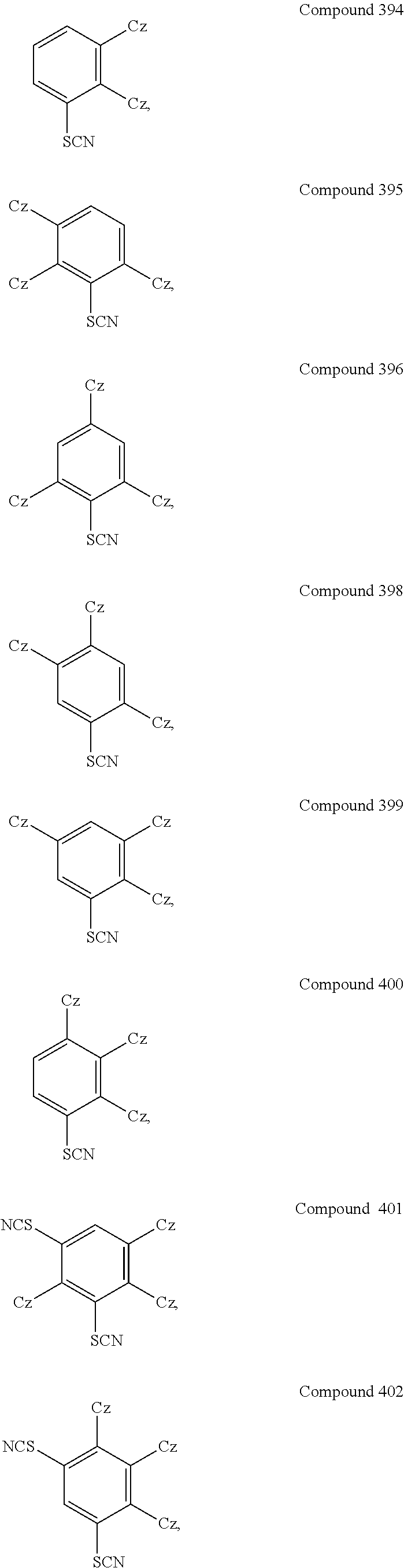
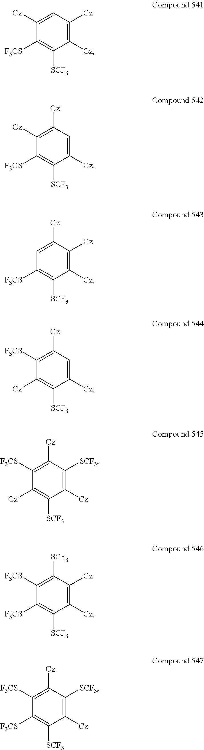
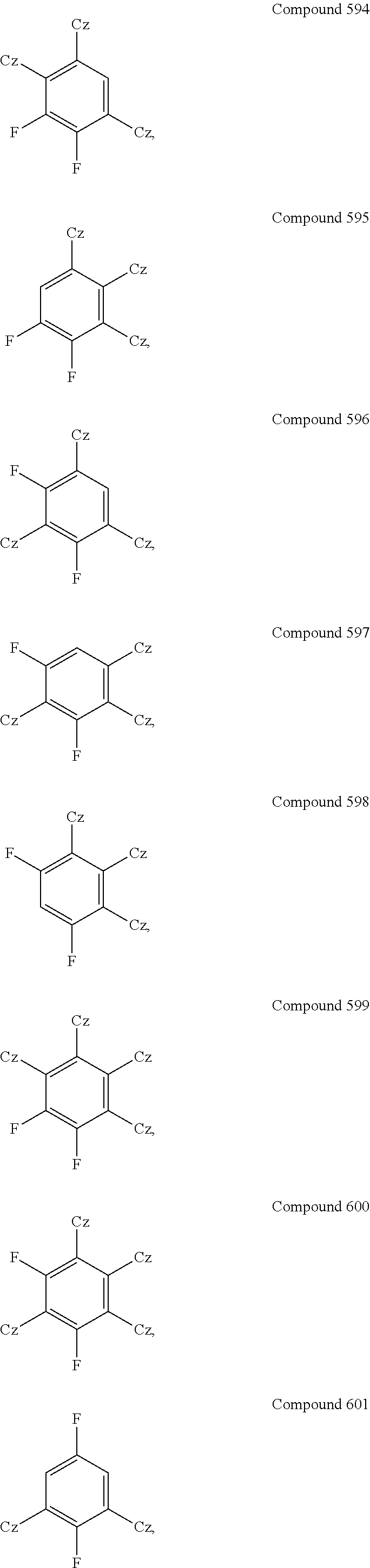
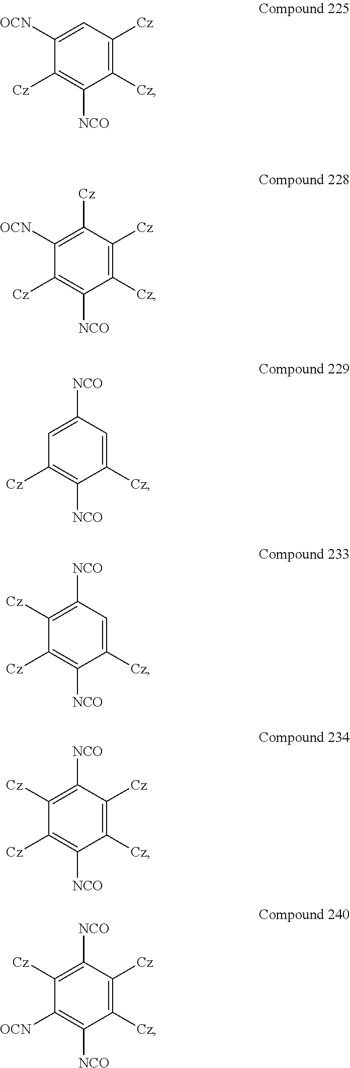
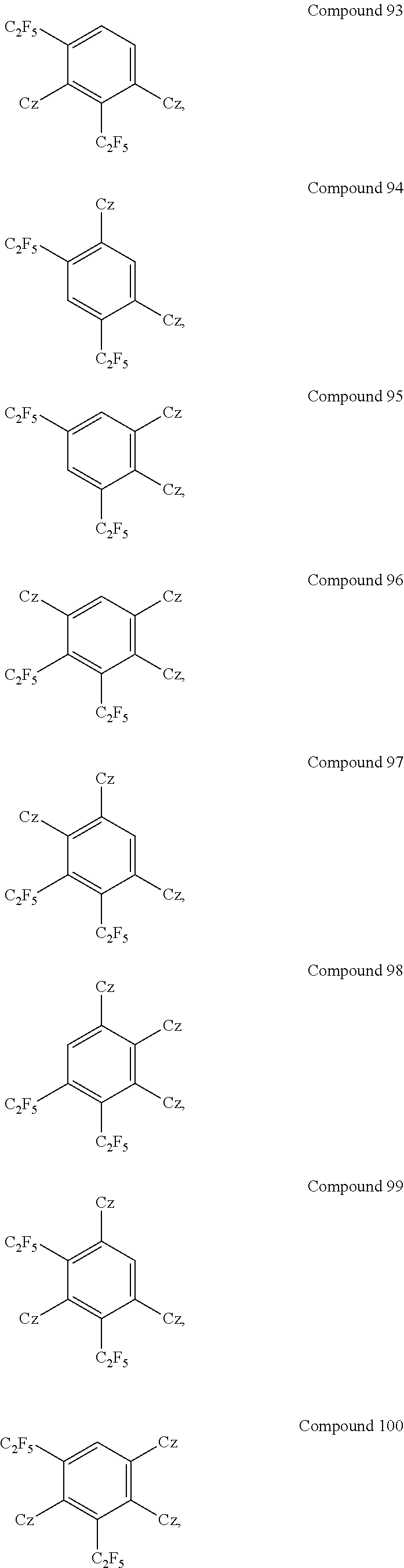
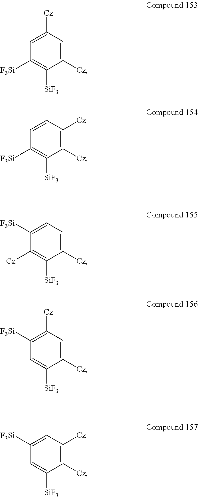
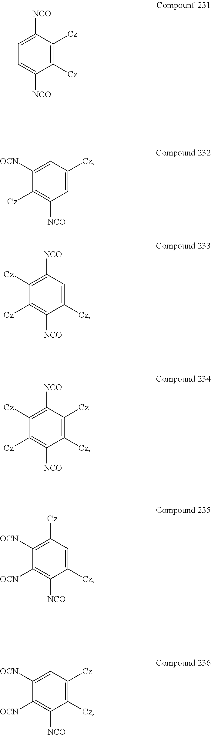
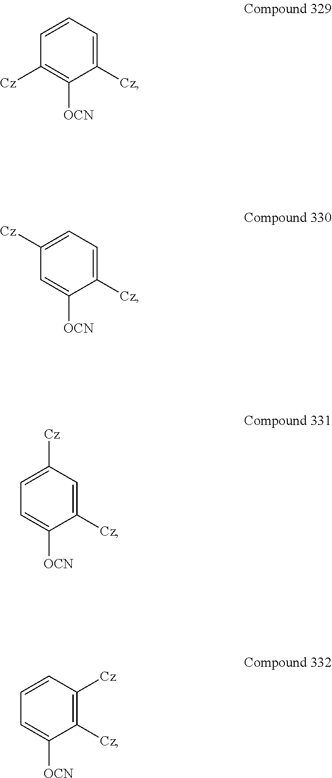
- the compound is selected from the group consisting of:
- R 5 is
- a 5 and A 6 are joined by a single bond. In some embodiments, B 5 and B 6 are joined by a single bond.
- At least one of R 2 -R 4 comprises an acceptor group selected from the group consisting of —C m F 2m+1 , —Si m F 2m+1 , —NCO, —NCS, —OCN, —SCN, —OC m F 2m+1 , and —SC m F 2m+1 .
- at least two of R 2 -R 4 comprise an acceptor group selected from the group consisting of —C m F 2m+1 , —Si m F 2m+1 , —NCO, —NCS, —OCN, —SCN, —OC m F 2m+1 , and —SC m F 2m+1 .
- At least three of R 2 -R 4 comprise an acceptor group selected from the group consisting of —C m F 2m+1 , —Si m F 2m+1 , —NCO, —NCS, —OCN, —SCN, —OC m F 2m+1 , and —SC m F 2m+1 .
- At least one of R 2 -R 4 is
- At least two of R 2 -R 4 are
- all three of R 2 -R 4 are
- At least one of R 2 -R 4 is an electron withdrawing group with a Hammett value ( ⁇ para ) of at least 0.05. In some embodiments, at least two of R 2 -R 4 are electron withdrawing groups with a Hammett value ( ⁇ para ) of at least 0.05. In some embodiments, at least three of R 2 -R 4 are electron withdrawing groups with a Hammett value ( ⁇ para ) of at least 0.05.
- the compound is selected from the group consisting of:
- a first device can include a first organic light emitting device that includes an anode; a cathode; and an emissive layer disposed between the anode and the cathode.
- the emissive layer can include a first emitting compound comprising a structure according to Formula 2:
- ring A is an aromatic or heteroaromatic ring
- n 0 or 1
- X 1 , X 2 , X 3 , X 4 , and X 5 are independently selected from the group consisting of CR, N, NR, O, S, and Se, and at least one of X 1 to X 5 is CR;
- X 1 , X 2 , X 3 , X 4 , X 5 , and X 6 are independently selected from the group consisting of CR and N, and at least one of X 1 to X 6 is CR;
- each R is independently selected from the group consisting of hydrogen, deuterium, halide, alkyl, haloalkyl, cycloalkyl, heteroalkyl, arylalkyl, alkoxy, thioalkoxy, aryloxy, thioaryloxy, amino, arylamino, diarylamino, carbazolyl, silyl, halosilyl, alkenyl, cycloalkenyl, heteroalkenyl, alkynyl, aryl, heteroaryl, acyl, carbonyl, carboxylic acids, ester, nitrile, isonitrile, sulfanyl, sulfinyl, sulfonyl, phosphino, —C m F 2m+1 , —Si m F 2m+1 , —NCO, —NCS, —OCN, —SCN, —OC m F 2m+1 , —SC m F 2m+1 ,
- R groups are, optionally, joined to form a fused ring structure
- At least one R group comprises a donor group with at least one electron-donating nitrogen
- At least one R group comprises an acceptor group selected from the group consisting of —F, —C m F 2m+1 , —Si m F 2m+1 , —NCO, —NCS, —OCN, —SCN, —OC m F 2m+1 , and —SC m F 2m+1 .
- At least two R groups comprise a donor group with at least one electron-donating nitrogen. In some embodiments, at least three R groups comprise a donor group with at least one electron-donating nitrogen, or at least four R groups comprise a donor group with at least one electron-donating nitrogen, or at least five R groups comprise a donor group with at least one electron-donating nitrogen. In some embodiments the donor group comprising at least one electron-donating nitrogen is a carbazole.
- At least two R groups comprise an acceptor group selected from the group consisting of —F, —C m F 2m+1 , —Si m F 2m+1 , —NCO, —NCS, —OCN, —SCN, —OC m F 2m+1 , and —SC m F 2m+1 .
- At least three R groups, at least four R groups, or at least five R groups comprise an acceptor group selected from the group consisting of —F, —C m F 2m+1 , —Si m F 2m+1 , —NCO, —NCS, —OCN, —SCN, —OC m F 2m+1 , and —SC m F 2m+1 .
- n 1
- at least two of X 1 to X 6 are CR, and at least two R groups are independently selected from the group consisting of —F, —C m F 2m+1 , —Si m F 2m+1 , —NCO, —NCS, —OCN, —SCN, —OC m F 2m+1 , and —SC m F 2m+1 .
- n 1 wherein at least two of X 1 to X 6 are CR, at least one R group is selected from the group consisting of —F, —C m F 2m+1 , —Si m F 2m+1 , —NCO, —NCS, —OCN, —SCN, —OC m F 2m+1 , and —SC m F 2m+1 , and at least one R is an electron withdrawing group with a Hammett value ( ⁇ para ) of at least 0.05.
- the compound in the emissive layer is a compound according to the structure of Formula 1, and all its variants, as described herein, with the provision that in addition to any other substituents listed for R 1 , R 2 , R 3 , R 4 , Y 1 , Y 2 , Y 3 , Y 4 , Y 5 , Y 6 , Y 7 , Y 8 , Z 1 , Z 2 , Z 3 , Z 4 , Z 5 , Z 6 , Z 7 , and Z 8 each of R 1 , R 2 , R 3 , R 4 , Y 1 , Y 2 , Y 3 , Y 4 , Y 5 , Y 6 , Y 7 , Y 8 , Z 1 , Z 2 , Z 3 , Z 4 , Z 5 , Z 6 , Z 7 , and Z 8 can independently also be —F.
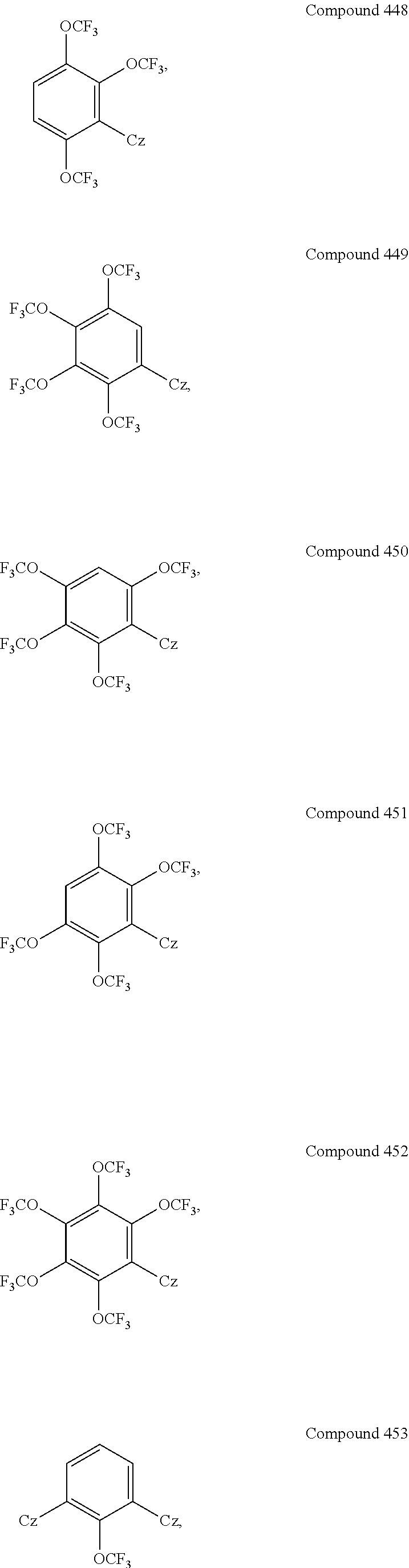
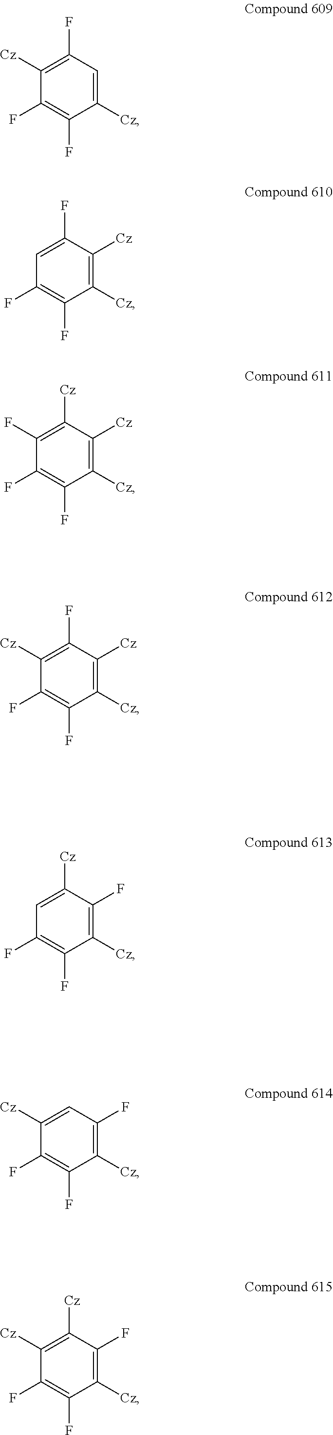
- the compound of formula 2 can be selected from the group consisting of:
- the compound comprises two structures according to Formula 2 bonded together.
- the two structures of Formula 2 are part of a fused ring system.
- At least one R group comprises the structure of Formula 3:
- R′, R′′, and R′′′ are independently aryl or heteroaryl.
- at least one of R′′ and R′′′ comprises a structure of Formula 2.
- the first device emits a luminescent radiation at room temperature when a voltage is applied across the organic light emitting device, and the luminescent radiation comprises a delayed fluorescence process.
- the emissive layer further comprises a host material. In some embodiments, the emissive layer further comprises a first phosphorescent emitting material. In some embodiments, the emissive layer also includes a second phosphorescent emitting material. In some embodiments, the first device emits a white light at room temperature when a voltage is applied across the organic light emitting device.
- the compound comprising a structure according to Formula 2 emits a blue light with a peak wavelength of about 400 nm to about 500 nm. In some embodiments, the compound comprising a structure according to Formula 2 emits a yellow light with a peak wavelength of about 530 nm to about 580 nm.
- a formulation that comprises a compound according to Formula 1 is described.
- the formulation can include one or more components selected from the group consisting of a solvent, a host, a hole injection material, hole transport material, and an electron transport layer material, disclosed herein.
- the materials described herein as useful for a particular layer in an organic light emitting device may be used in combination with a wide variety of other materials present in the device.
- emissive dopants disclosed herein may be used in conjunction with a wide variety of hosts, transport layers, blocking layers, injection layers, electrodes and other layers that may be present.
- the materials described or referred to below are non-limiting examples of materials that may be useful in combination with the compounds disclosed herein, and one of skill in the art can readily consult the literature to identify other materials that may be useful in combination.
- a hole injecting/transporting material to be used in the present invention is not particularly limited, and any compound may be used as long as the compound is typically used as a hole injecting/transporting material.
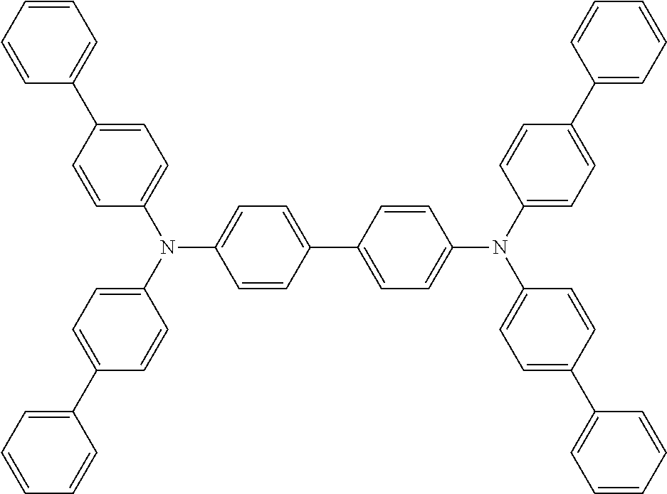
- the material include, but not limit to: a phthalocyanine or porphyrin derivative; an aromatic amine derivative; an indolocarbazole derivative; a polymer containing fluorohydrocarbon; a polymer with conductivity dopants; a conducting polymer, such as PEDOT/PSS; a self-assembly monomer derived from compounds such as phosphonic acid and silane derivatives; a metal oxide derivative, such as MoO x ; a p-type semiconducting organic compound, such as 1,4,5,8,9,12-Hexaazatriphenylenehexacarbonitrile; a metal complex, and a cross-linkable compounds.
- aromatic amine derivatives used in HIL or HTL include, but not limit to the following general structures:
- Each of Ar 1 to Ar 9 is selected from the group consisting of aromatic hydrocarbon cyclic compounds such as benzene, biphenyl, triphenyl, triphenylene, naphthalene, anthracene, phenalene, phenanthrene, fluorene, pyrene, chrysene, perylene, and azulene; the group consisting of aromatic heterocyclic compounds such as dibenzothiophene, dibenzofuran, dibenzoselenophene, furan, thiophene, benzofuran, benzothiophene, benzoselenophene, carbazole, indolocarbazole, pyridylindole, pyrrolodipyridine, pyrazole, imidazole, triazole, oxazole, thiazole, oxadiazole, oxatriazole, dioxazole, thiadiazole, pyridine, pyridazine
- each Ar is further substituted by a substituent selected from the group consisting of hydrogen, deuterium, halide, alkyl, cycloalkyl, heteroalkyl, arylalkyl, alkoxy, aryloxy, amino, silyl, alkenyl, cycloalkenyl, heteroalkenyl, alkynyl, aryl, heteroaryl, acyl, carbonyl, carboxylic acids, ester, nitrile, isonitrile, sulfanyl, sulfinyl, sulfonyl, phosphino, and combinations thereof.
- a substituent selected from the group consisting of hydrogen, deuterium, halide, alkyl, cycloalkyl, heteroalkyl, arylalkyl, alkoxy, aryloxy, amino, silyl, alkenyl, cycloalkenyl, heteroalkenyl, alkynyl, aryl, heteroaryl, acy
- Ar 1 to Ar 9 is independently selected from the group consisting of:
- k is an integer from 1 to 20;
- X 101 to X 107 is C (including CH) or N;
- Z 101 is NAr 1 , O, or S;
- Ar 1 has the same group defined above.
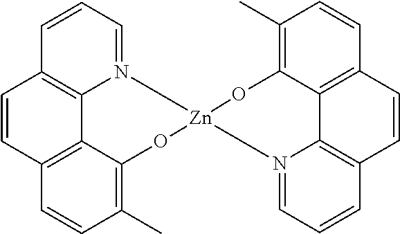
- metal complexes used in HIL or HTL include, but not limit to the following general formula:
- Met is a metal, which can have an atomic weight greater than 40;
- (Y 101 -Y 102 ) is a bidentate ligand, Y 101 and Y 102 are independently selected from C, N, O, P, and S;
- L 101 is an ancillary ligand;
- k′ is an integer value from 1 to the maximum number of ligands that may be attached to the metal; and
- k′+k′′ is the maximum number of ligands that may be attached to the metal.
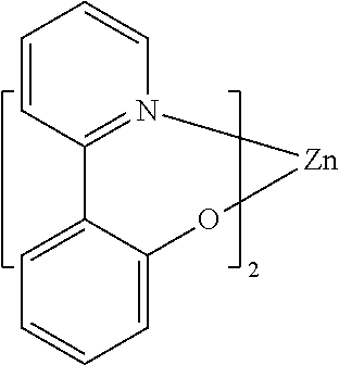
- (Y 101 -Y 102 ) is a 2-phenylpyridine derivative. In another aspect, (Y 101 -Y 102 ) is a carbene ligand. In another aspect, Met is selected from Ir, Pt, Os, and Zn. In a further aspect, the metal complex has a smallest oxidation potential in solution vs. Fc + /Fc couple less than about 0.6 V.
- the light emitting layer of the organic EL device of the present invention preferably contains at least a metal complex as light emitting material, and may contain a host material using the metal complex as a dopant material.
- the host material are not particularly limited, and any metal complexes or organic compounds may be used as long as the triplet energy of the host is larger than that of the dopant. While the Table below categorizes host materials as preferred for devices that emit various colors, any host material may be used with any dopant so long as the triplet criteria is satisfied.
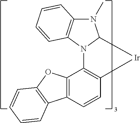
- metal complexes used as host are preferred to have the following general formula:
- Met is a metal
- (Y 103 -Y 104 ) is a bidentate ligand, Y 103 and Y 104 are independently selected from C, N, O, P, and S
- L 101 is an another ligand
- k′ is an integer value from 1 to the maximum number of ligands that may be attached to the metal
- k′+k′′ is the maximum number of ligands that may be attached to the metal.
- the metal complexes are:
- (O—N) is a bidentate ligand, having metal coordinated to atoms O and N.
- Met is selected from Ir and Pt.
- (Y 103 -Y 104 ) is a carbene ligand.
- organic compounds used as host are selected from the group consisting of aromatic hydrocarbon cyclic compounds such as benzene, biphenyl, triphenyl, triphenylene, naphthalene, anthracene, phenalene, phenanthrene, fluorene, pyrene, chrysene, perylene, and azulene; the group consisting of aromatic heterocyclic compounds such as dibenzothiophene, dibenzofuran, dibenzoselenophene, furan, thiophene, benzofuran, benzothiophene, benzoselenophene, carbazole, indolocarbazole, pyridylindole, pyrrolodipyridine, pyrazole, imidazole, triazole, oxazole, thiazole, oxadiazole, oxatriazole, dioxazole, thiadiazole, pyridine, pyridazine,
- each group is further substituted by a substituent selected from the group consisting of hydrogen, deuterium, halide, alkyl, cycloalkyl, heteroalkyl, arylalkyl, alkoxy, aryloxy, amino, silyl, alkenyl, cycloalkenyl, heteroalkenyl, alkynyl, aryl, heteroaryl, acyl, carbonyl, carboxylic acids, ester, nitrile, isonitrile, sulfanyl, sulfinyl, sulfonyl, phosphino, and combinations thereof.
- a substituent selected from the group consisting of hydrogen, deuterium, halide, alkyl, cycloalkyl, heteroalkyl, arylalkyl, alkoxy, aryloxy, amino, silyl, alkenyl, cycloalkenyl, heteroalkenyl, alkynyl, aryl, heteroaryl, acy
- host compound contains at least one of the following groups in the molecule:
- R 101 to R 107 is independently selected from the group consisting of hydrogen, deuterium, halide, alkyl, cycloalkyl, heteroalkyl, arylalkyl, alkoxy, aryloxy, amino, silyl, alkenyl, cycloalkenyl, heteroalkenyl, alkynyl, aryl, heteroaryl, acyl, carbonyl, carboxylic acids, ester, nitrile, isonitrile, sulfanyl, sulfinyl, sulfonyl, phosphino, and combinations thereof, when it is aryl or heteroaryl, it has the similar definition as Ar's mentioned above.
- X 1101 to X 108 is selected from C (including CH) or N.
- Z 101 and Z 102 is selected from NR 101 , O, or S.
- HBL HBL
- a hole blocking layer may be used to reduce the number of holes and/or excitons that leave the emissive layer.
- the presence of such a blocking layer in a device may result in substantially higher efficiencies as compared to a similar device lacking a blocking layer.
- a blocking layer may be used to confine emission to a desired region of an OLED.
- compound used in HBL contains the same molecule or the same functional groups used as host described above.
- compound used in HBL contains at least one of the following groups in the molecule:
- Electron transport layer may include a material capable of transporting electrons. Electron transport layer may be intrinsic (undoped), or doped. Doping may be used to enhance conductivity. Examples of the ETL material are not particularly limited, and any metal complexes or organic compounds may be used as long as they are typically used to transport electrons.
- compound used in ETL contains at least one of the following groups in the molecule:
- R 101 is selected from the group consisting of hydrogen, deuterium, halide, alkyl, cycloalkyl, heteroalkyl, arylalkyl, alkoxy, aryloxy, amino, silyl, alkenyl, cycloalkenyl, heteroalkenyl, alkynyl, aryl, heteroaryl, acyl, carbonyl, carboxylic acids, ester, nitrile, isonitrile, sulfanyl, sulfinyl, sulfonyl, phosphino, and combinations thereof, when it is aryl or heteroaryl, it has the similar definition as Ar's mentioned above.
- Ar 1 to Ar 3 has the similar definition as Ar's mentioned above.
- k is an integer from 1 to 20.
- X 101 to X 108 is selected from C (including CH) or N.
- the metal complexes used in ETL contains, but not limit to the following general formula:
- (O—N) or (N—N) is a bidentate ligand, having metal coordinated to atoms O, N or N, N; L 101 is another ligand; k′ is an integer value from 1 to the maximum number of ligands that may be attached to the metal.
- the hydrogen atoms can be partially or fully deuterated.
- any specifically listed substituent such as, without limitation, methyl, phenyl, pyridyl, etc. encompasses undeuterated, partially deuterated, and fully deuterated versions thereof.
- classes of substituents such as, without limitation, alkyl, aryl, cycloalkyl, heteroaryl, etc. also encompass undeuterated, partially deuterated, and fully deuterated versions thereof.
- hole injection materials In addition to and/or in combination with the materials disclosed herein, many hole injection materials, hole transporting materials, host materials, dopant materials, exiton/hole blocking layer materials, electron transporting and electron injecting materials may be used in an OLED.
- Non-limiting examples of the materials that may be used in an OLED in combination with materials disclosed herein are listed in Table A below. Table A lists non-limiting classes of materials, non-limiting examples of compounds for each class, and references that disclose the materials.
- Triarylamine or polythiophene polymers with conductivity dopants EP1725079A1 and Organic compounds with conductive inorganic compounds, such as molybdenum tungsten oxides US20050123751 SID Symposium Digest, 37, 923 (2006) WO2009018009 n-type semiconducting organic complexes US20020158242 Metal organometallic complexes US20060240279 Cross-linkable compounds US20080220265 Polythiophene based polymers and copolymers WO 2011075644 EP2350216 Hole transporting materials Triarylamines (e.g., TPD, ⁇ -NPD) Appl.
- Triarylamines e.g., TPD, ⁇ -NPD
- Metal 8- hydroxyquinolates e.g., BAlq
- Appl. Phys. Lett. 81, 162 (2002) 5-member ring electron deficient heterocycles such as triazole, oxadiazole, imidazole, benzoimidazole Appl. Phys. Lett. 81, 162 (2002) Triphenylene compounds US20050025993 Fluorinated aromatic compounds Appl. Phys. Lett.
- Carbazole (5.3 g, 32.0 mmol) and sodium hydride (1.9 g, 47.0 mmol) were mixed in 50 mL of dry (i.e., anhydrous) dimethylformamide (DMF). The solution was stirred for 1 hour at room temperature. Octafluorotoluene (0.5 g, 2.2 mmol) was added to the solution. The mixture was then stirred for 3 days under nitrogen. The reaction mixture was poured into water and the precipitate was filtered. The residue was then suspended in tetrahydrofuran (THF):heptane (1:3, v/v) and heated for 1 hour. After cooling, 1.3 g (61%) of compound 14 was obtained as a pale yellow solid by filtration.
- THF tetrahydrofuran
- Carbazole (2.9 g, 17 mmol) and sodium hydride (1 g, 25 mmol) were mixed in 30 mL of dry DMF. The solution was stirred for 1 hour at room temperature. 2,3,5,6-tetrafluorobenzotrifluoride (0.38 g, 1.7 mmol) was then added to the mixture. The mixture was stirred for 3 days under nitrogen. The reaction mixture was poured into water and the precipitate was filtered. The residue was then suspended in THF:heptane (1:3, v/v) and heated for 1 hour. Upon cooling, 1.0 g (71%) of compound 12 was obtained as a white solid by filtration.
- N 1 ,N 1 ,N 4 -triphenylbenzene-1,4-diamine (1.0 g, 3.0 mmol) and 1-bromo-3,5-bis(trifluoromethyl)benzene (1.15 g, 3.9 mmol) were mixed in 70 mL of dry xylene. The solution was bubbled with nitrogen for 15 min.
- Pd 2 (dba) 3 (0.29 g, 0.32 mmol)
- 2-dicyclohexylphosphino-2′,6′-dimethoxybiphenyl (0.58 g, 1.20 mmol)
- t BuONa (0.44 g, 4.50 mmol
- Carbazole (19.6 g, 117.6 mmol) and sodium hydride (7.0 g, 176.4 mmol) were mixed in 300 mL of dry 1,2-dimethoxyethane. The solution was stirred for 2 hours and 1,2,3,4,5-pentafluoro-6-isothiocyanatobenzene (2.0 g, 7.8 mmol) was added. The mixture was stirred under nitrogen for 1 week at room temperature. The reaction mixture was poured into water and the precipitate was filtered. The residue was then purified by column chromatography using gradient from hexane to toluene:hexane (1:1, v/v) as the eluent. 1.9 g (25%) of Compound 262 and 0.3 g (5%) of Compound 736 were collected.
- Carbazole (4.0 g, 23.8 mmol) and sodium hydride (1.4 g, 35.7 mmol) were mixed in 60 mL of dry 1,2-dimethoxyethane. The solution was stirred for 2 hours, then 1,3,5-trifluoro-2-isothiocyanatobenzene (0.5 g, 2.6 mmol) was added to the solution. The mixture was stirred under nitrogen for 4 days at room temperature. The reaction mixture was poured into water and the precipitate was filtered. The residue was then purified by column chromatography using gradient from hexane to toluene:hexane (1:1, v/v) as the eluent. 57 mg (3%) of Compound 254 was isolated.
- the organic stack of the Device Examples in Table 3 consists of, sequentially from the ITO surface, 100 ⁇ of LG101 as the hole injection layer (HIL), 300 ⁇ of TAPC as the hole transporting layer (HTL), 300 ⁇ of mCP doped with 10% or 15% or neat of dopant Compound 11 or 12 or 14 as the emissive layer (EML), 0 or 50 ⁇ of Compound A or B as the ETL2, and 400 ⁇ of TmPyPB or LG201 as the ETL1.
- HIL hole injection layer
- HTL hole transporting layer
- EML emissive layer
- ETL2 emissive layer
- Device 3 with Compound 14 as the emitter has an external quantum efficiency of 10% at 100 cd/m 2 and 8.1% at 100 cd/m 2 .
- the result demonstrates that charge transfer luminescent compounds with strong acceptors as emitters in OLED can lead to device efficiency higher than the theoretical limit of fluorescent OLED, by harvesting the triplet through delayed fluorescence.
Abstract

as well as, a first device and a formulation including the same are disclosed. In the structure of Formula 1:
-
- R5 is

and
-
- (a) at least one of R1-R4 is

or (b) R1 is

Description


is described.
In the structure according to Formula 1:

and

or (b) R1 is


In the compound of

is described. In the structure according to Formula 1:

and

or (b) is


and at least one of R1-R4 is

In some embodiments, at least two of R1-R4 are

In some embodiments, at least three of R1-R4 are

while all four of R1-R4 are

in other embodiments.


As used herein, Cz is


and R1 is

In some embodiments, A5 and A6 are joined by a single bond. In some embodiments, B5 and B6 are joined by a single bond.

In some embodiments, at least two of R2-R4 are

In some embodiments, all three of R2-R4 are


As used herein, Cz is


In the compound of


As used herein Cz is


wherein R′, R″, and R′″ are independently aryl or heteroaryl. In some embodiments, at least one of R″ and R′″ comprises a structure of


wherein k is an integer from 1 to 20; X101 to X107 is C (including CH) or N; Z101 is NAr1, O, or S; Ar1 has the same group defined above.
wherein Met is a metal, which can have an atomic weight greater than 40; (Y101-Y102) is a bidentate ligand, Y101 and Y102 are independently selected from C, N, O, P, and S; L101 is an ancillary ligand; k′ is an integer value from 1 to the maximum number of ligands that may be attached to the metal; and k′+k″ is the maximum number of ligands that may be attached to the metal.

wherein Met is a metal; (Y103-Y104) is a bidentate ligand, Y103 and Y104 are independently selected from C, N, O, P, and S; L101 is an another ligand; k′ is an integer value from 1 to the maximum number of ligands that may be attached to the metal; and k′+k″ is the maximum number of ligands that may be attached to the metal.

wherein (O—N) is a bidentate ligand, having metal coordinated to atoms O and N.


wherein R101 to R107 is independently selected from the group consisting of hydrogen, deuterium, halide, alkyl, cycloalkyl, heteroalkyl, arylalkyl, alkoxy, aryloxy, amino, silyl, alkenyl, cycloalkenyl, heteroalkenyl, alkynyl, aryl, heteroaryl, acyl, carbonyl, carboxylic acids, ester, nitrile, isonitrile, sulfanyl, sulfinyl, sulfonyl, phosphino, and combinations thereof, when it is aryl or heteroaryl, it has the similar definition as Ar's mentioned above. k is an integer from 0 to 20 or 1 to 20; k′″ is an integer from 0 to 20. X1101 to X108 is selected from C (including CH) or N. Z101 and Z102 is selected from NR101, O, or S.
HBL:

wherein k is an integer from 1 to 20; L101 is an another ligand, k′ is an integer from 1 to 3.
ETL:

wherein R101 is selected from the group consisting of hydrogen, deuterium, halide, alkyl, cycloalkyl, heteroalkyl, arylalkyl, alkoxy, aryloxy, amino, silyl, alkenyl, cycloalkenyl, heteroalkenyl, alkynyl, aryl, heteroaryl, acyl, carbonyl, carboxylic acids, ester, nitrile, isonitrile, sulfanyl, sulfinyl, sulfonyl, phosphino, and combinations thereof, when it is aryl or heteroaryl, it has the similar definition as Ar's mentioned above. Ar1 to Ar3 has the similar definition as Ar's mentioned above. k is an integer from 1 to 20. X101 to X108 is selected from C (including CH) or N.

wherein (O—N) or (N—N) is a bidentate ligand, having metal coordinated to atoms O, N or N, N; L101 is another ligand; k′ is an integer value from 1 to the maximum number of ligands that may be attached to the metal.
| TABLE A | ||
| MATERIAL | EXAMPLES OF MATERIAL | PUBLICATIONS |
| Hole injection materials |
| Phthalocyanine and porphyrin compounds |
 |
Appl. Phys. Lett. 69, 2160 (1996) |
| Starburst triarylamines |
 |
J. Lumin. 72-74, 985 (1997) |
| CFx Fluorohydrocarbon polymer |
|
Appl. Phys. Lett. 78, 673 (2001) |
| Conducting polymers (e.g., PEDOT:PSS, polyaniline, polythiophene) |
 |
Synth. Met. 87, 171 (1997) WO2007002683 |
| Phosphonic acid and silane SAMs |
|
US20030162053 |
| Triarylamine or polythiophene polymers with conductivity dopants |
 |
EP1725079A1 |
| and | ||
 |
||
 |
||
| Organic compounds with conductive inorganic compounds, such as molybdenum tungsten oxides |
 |
US20050123751 SID Symposium Digest, 37, 923 (2006) WO2009018009 |
| n-type semiconducting organic complexes |
 |
US20020158242 |
| Metal organometallic complexes |
 |
US20060240279 |
| Cross-linkable compounds |
 |
US20080220265 |
| Polythiophene based polymers and copolymers |
 |
WO 2011075644 EP2350216 |
| Hole transporting materials |
| Triarylamines (e.g., TPD, α-NPD) |
 |
Appl. Phys. Lett. 51, 913 (1987) |
 |
US5061569 | |
 |
EP650955 | |
 |
J. Mater. Chem. 3, 319 (1993) | |
 |
Appl. Phys. Lett. 90, 183503 (2007) | |
 |
Appl. Phys. Lett. 90, 183503 (2007) | |
| Triarylamine on spirofluorene core |
 |
Synth. Met. 91, 209 (1997) |
| Arylamine carbazole compounds |
 |
Adv. Mater. 6, 677 (1994), US20080124572 |
| Triarylamine with (di)benzothiophene/ (di)benzofuran |
 |
US200702789238, US20080106190 US20110163302 |
| Indolocarbazoles |
 |
Synth. Met. 111, 421 (2000) |
| Isoindole compounds |
 |
Chem. Mater. 15, 3148 (2003) |
| Metal carbene complexes |
 |
US20080018221 |
| Phosphorescent OLED host materials |
| Red hosts |
| Arylcarbazoles |
 |
Appl. Phys. Lett. 78, 1622 (2001) |
| Metal 8- hydroxyquinolates (e.g., Alq3, BAlq) |
 |
Nature 395, 151 (1998) |
 |
US20060202194 | |
 |
WO2005014551 | |
 |
WO2006072002 | |
| Metal phenoxybenzothiazole compounds |
 |
Appl. Phys. Lett. 90, 123509 (2007) |
| Conjugated oligomers and polymers (e.g., polyfluorene) |
 |
Org. Electron. 1, 15 (2000) |
| Aromatic fused rings |
 |
WO2009066779, WO2009066778, WO2009063833, US20090045731, US20090045730, WO2009008311, US20090008605, US20090009065 |
| Zinc complexes |
 |
WO2010056066 |
| Chrysene based compounds |
 |
WO2011086863 |
| Green hosts |
| Arylcarbazoles |
 |
Appl. Phys. Lett. 78, 1622 (2001) |
 |
US20030175553 | |
 |
WO2001039234 | |
| Aryltriphenylene compounds |
 |
US20060280965 |
 |
US20060280965 | |
 |
WO2009021126 | |
| Poly-fused heteroaryl compounds |
 |
US20090309488 US20090302743 US20100012931 |
| Donor acceptor type molecules |
 |
WO2008056746 |
 |
WO2010107244 | |
| Aza-carbazole/ DBT/DBF |
 |
JP2008074939 |
 |
US20100187984 | |
| Polymers (e.g., PVK) |
 |
Appl. Phys. Lett. 77, 2280 (2000) |
| Spirofluorene compounds |
 |
WO2004093207 |
| Metal phenoxybenzooxazole compounds |
 |
WO2005089025 |
 |
WO2006132173 | |
 |
JP200511610 | |
| Spirofluorene- carbazole compounds |
 |
JP2007254297 |
 |
JP2007254297 | |
| Indolocarbazoles |
 |
WO2007063796 |
 |
WO2007063754 | |
| 5-member ring electron deficient heterocycles (e.g., triazole, oxadiazole) |
 |
J. Appl. Phys. 90, 5048 (2001) |
 |
WO2004107822 | |
| Tetraphenylene complexes |
 |
US20050112407 |
| Metal phenoxypyridine compounds |
 |
WO2005030900 |
| Metal coordination complexes (e.g., Zn, Al with N{circumflex over ( )}N ligands) |
 |
US20040137268, US20040137267 |
| Blue hosts |
| Arylcarbazoles |
 |
Appl. Phys. Lett, 82, 2422 (2003) |
 |
US20070190359 | |
| Dibenzothiophene/ Dibenzofuran- carbazole compounds |
 |
WO2006114966, US20090167162 |
 |
US20090167162 | |
 |
WO2009086028 | |
 |
US20090030202, US20090017330 | |
 |
US20100084966 | |
| Silicon aryl compounds |
 |
US20050238919 |
 |
WO2009003898 | |
| Silicon/Germanium aryl compounds |
 |
EP2034538A |
| Aryl benzoyl ester |
 |
WO2006100298 |
| Carbazole linked by non-conjugated groups |
 |
US20040115476 |
| Aza-carbazoles |
 |
US20060121308 |
| High triplet metal organometallic complex |
 |
US7154114 |
| Phosphorescent dopants |
| Red dopants |
| Heavy metal porphyrins (e.g., PtOEP) |
 |
Nature 395, 151 (1998) |
| Iridium (III) organometallic complexes |
 |
Appl. Phys. Lett. 78, 1622 (2001) |
 |
US20030072964 | |
 |
US20030072964 | |
 |
US20060202194 | |
 |
US20060202194 | |
 |
US20070087321 | |
 |
US20080261076 US20100090591 | |
 |
US20070087321 | |
 |
Adv. Mater. 19, 739 (2007) | |
 |
WO2009100991 | |
 |
WO2008101842 | |
 |
US7232618 | |
| Platinum (II) organometallic complexes |
 |
WO2003040257 |
 |
US20070103060 | |
| Osmium (III) complexes |
 |
Chem. Mater. 17, 3532 (2005) |
| Ruthenium (II) complexes |
 |
Adv. Mater. 17, 1059 (2005) |
| Rhenium (I), (II), and (III) complexes |
 |
US20050244673 |
| Green dopants Iridium (III) organometallic complexes |
 |
Inorg. Chem. 40, 1704 (2001) |
 |
US20020034656 | |
 |
US7332232 | |
 |
US20090108737 | |
 |
WO2010028151 | |
 |
EP1841834B | |
 |
US20060127696 | |
 |
US20090039776 | |
 |
US6921915 | |
 |
US20100244004 | |
 |
US6687266 | |
 |
Chem. Mater. 16, 2480 (2004) | |
 |
US20070190359 | |
 |
US 20060008670 JP2007123392 | |
 |
WO2010086089, WO2011044988 | |
 |
Adv. Mater. 16, 2003 (2004) | |
 |
Angew. Chem. Int. Ed. 2006, 45, 7800 | |
 |
WO2009050290 | |
 |
US20090165846 | |
 |
US20080015355 | |
 |
US20010015432 | |
 |
US20100295032 | |
| Monomer for polymeric metal organometallic compounds |
 |
US7250226, US7396598 |
| Pt (II) organometallic complexes, including polydentated ligands |
 |
Appl. Phys. Lett. 86, 153505 (2005) |
 |
Appl. Phys. Lett. 86, 153505 (2005) | |
 |
Chem. Lett. 34, 592 (2005) | |
 |
WO2002015645 | |
 |
US20060263635 | |
 |
US20060182992 US20070103060 | |
| Cu complexes |
 |
WO2009000673 |
 |
US20070111026 | |
| Gold complexes |
 |
Chem. Commun. 2906 (2005) |
| Rhenium (III) complexes |
 |
Inorg. Chem. 42, 1248 (2003) |
| Osmium (II) complexes |
 |
US7279704 |
| Deuterated organometallic complexes |
 |
US20030138657 |
| Organometallic complexes with two or more metal centers |
 |
US20030152802 |
 |
US7090928 | |
| Blue dopants |
| Iridium (III) organometallic complexes |
 |
WO2002002714 |
 |
WO2006009024 | |
 |
US20060251923 US20110057559 US20110204333 | |
 |
US7393599, WO2006056418, US20050260441, WO2005019373 | |
 |
US7534505 | |
 |
WO2011051404 | |
 |
US7445855 | |
 |
US20070190359, US20080297033 US20100148663 | |
 |
US7338722 | |
 |
US20020134984 | |
 |
Angew. Chem. Int. Ed. 47, 4542 (2008) | |
 |
Chem. Mater. 18, 5119 (2006) | |
 |
Inorg. Chem. 46, 4308 (2007) | |
 |
WO2005123873 | |
 |
WO2005123873 | |
 |
WO2007004380 | |
 |
WO2006082742 | |
| Osmium (II) complexes |
 |
US7279704 |
 |
Organometallics 23, 3745 (2004) | |
| Gold complexes |
|
Appl. Phys. Lett. 74, 1361 (1999) |
| Platinum (II) complexes |
 |
WO2006098120, WO2006103874 |
| Pt tetradenate complexes with at least one metal- carbene bond |
 |
US7655323 |
| Exciton/hole blocking layer materials |
| Bathocuprine compounds (e.g., BCP, BPhen) |
 |
Appl. Phys. Lett. 75, 4 (1999) |
 |
Appl. Phys. Lett. 79, 449 (2001) | |
| Metal 8- hydroxyquinolates (e.g., BAlq) |
 |
Appl. Phys. Lett. 81, 162 (2002) |
| 5-member ring electron deficient heterocycles such as triazole, oxadiazole, imidazole, benzoimidazole |
 |
Appl. Phys. Lett. 81, 162 (2002) |
| Triphenylene compounds |
 |
US20050025993 |
| Fluorinated aromatic compounds |
 |
Appl. Phys. Lett. 79, 156 (2001) |
| Phenothiazine-S-oxide |
 |
WO20080132085 |
| Silylated five- membered nitrogen, oxygen, sulfur or phosphorus dibenzoheterocycles |
 |
WO2010079051 |
| Aza-carbazoles |
 |
US20060121308 |
| Electron transporting materials |
| Anthracene- benzoimidazole compounds |
 |
WO2003060956 |
 |
US20090179554 | |
| Aza triphenylene derivatives |
 |
US20090115316 |
| Anthracene- benzothiazole compounds |
 |
Appl. Phys. Lett. 89, 063504 (2006) |
| Metal 8- hydroxyquinolates (e.g., Alq3, Zrq4) |
 |
Appl. Phys. Lett. 51, 913 (1987) US7230107 |
| Metal hydroxy- benzoquinolates |
 |
Chem. Lett. 5, 905 (1993) |
| Bathocuprine compounds such as BCP, BPhen, etc |
 |
Appl. Phys. Lett. 91, 263503 (2007) |
 |
Appl. Phys. Lett. 79, 449 (2001) | |
| 5-member ring electron deficient heterocycles (e.g., triazole, oxadiazole, imidazole, benzoimidazole) |
 |
Appl. Phys. Lett. 74, 865 (1999) |
 |
Appl. Phys. Lett. 55, 1489 (1989) | |
 |
Jpn. J. Apply. Phys. 32, L917 (1993) | |
| Silole compounds |
 |
Org. Electron. 4, 113 (2003) |
| Arylborane compounds |
 |
J. Am. Chem. Soc. 120, 9714 (1998) |
| Fluorinated aromatic compounds |
 |
J. Am. Chem. Soc. 122, 1832 (2000) |
| Fullerene (e.g., C60) |
 |
US20090101870 |
| Triazine complexes |
 |
US20040036077 |
| Zn (N{circumflex over ( )}N) complexes |
 |
US6528187 |


| TABLE 1 | ||
| PLQY in PMMA | Emmax in | |
| Cmpd | (5 wt % of Cmpd) | PMMA [nm] |
| 14 | 53% | 475 |
| 743 | 5% | 493 |
| 262 | 16% | 489 |
| 736 | 10% | 406 |
| 12 | 21% | 423 |
| 11 | 55% | 436 |
| 254 | 5% | 406 |
| 32 | 42% | 433 |
| TABLE 2 | ||||
| Emmax at RT | Emmax at RT | Emmax at RT | Emmax at 77 K | |
| in 2Me—THF | in toluene | in 3-MP | in 3-MP | |
| Cmpd | [nm] | [nm] | [nm] | [nm] |
| 14 | 494 | 487 | 459 | 452 |
| 743 | 522 | 510 | 468 | 458 |
| 12 | 443 | 431 | 421 | 440 |
| 11 | 446 | 441 | 432 | 436 |
| 32 | 448 | 430 | 403 | 439 |
| TABLE 3 | |||||
| EML | 1931 CIE | At 1,000 nits | |||
| Host | dopant | ETL1 | CIE | CIE | Emmax | FWHM | V | LE | EQE | PE | ||
| Example | 300Å | [conc. %] | ETL250Å | 400Å | x | y | [nm] | [nm] | [V] | [cd/A] | [%] | [lm/W] |
| |
Cmpd 14 [100] | A | TmPyPB | 0.215 | 0.393 | 490 | 88 | 7.4 | 6.6 | 2.8 | 2.8 | |
| |
Cmpd 14 [100] | — | TmPyPB | 0.211 | 0.392 | 490 | 86 | 7.0 | 7.8 | 3.3 | 3.5 | |
| Device 3 | mCP | Cmpd 14 [0] | A | TmPyPB | 0.177 | 0.319 | 482 | 78 | 8.0 | 16.3 | 8.1 | 6.4 |
| Device 4 | mCP | Cmpd 14 [0] | — | TmPyPB | 0.174 | 0.295 | 482 | 76 | 8.3 | 11.0 | 5.7 | 4.2 |
| Device 5 | Cmpd 12 [100] | A | TmPyPB | 0.191 | 0.197 | 458 | 88 | 12.6 | 0.8 | 0.6 | 0.2 | |

Claims (25)


Priority Applications (3)
| Application Number | Priority Date | Filing Date | Title |
|---|---|---|---|
| US14/464,430 US9647218B2 (en) | 2013-11-14 | 2014-08-20 | Organic electroluminescent materials and devices |
| KR1020140154391A KR102289799B1 (en) | 2013-11-14 | 2014-11-07 | Organic electroluminescent materials and devices |
| JP2014230688A JP6628470B2 (en) | 2013-11-14 | 2014-11-13 | Organic electroluminescent material and device |
Applications Claiming Priority (2)
| Application Number | Priority Date | Filing Date | Title |
|---|---|---|---|
| US201361904098P | 2013-11-14 | 2013-11-14 | |
| US14/464,430 US9647218B2 (en) | 2013-11-14 | 2014-08-20 | Organic electroluminescent materials and devices |
Publications (2)
| Publication Number | Publication Date |
|---|---|
| US20150129849A1 US20150129849A1 (en) | 2015-05-14 |
| US9647218B2 true US9647218B2 (en) | 2017-05-09 |
Family
ID=53042963
Family Applications (1)
| Application Number | Title | Priority Date | Filing Date |
|---|---|---|---|
| US14/464,430 Active 2035-04-08 US9647218B2 (en) | 2013-11-14 | 2014-08-20 | Organic electroluminescent materials and devices |
Country Status (3)
| Country | Link |
|---|---|
| US (1) | US9647218B2 (en) |
| JP (1) | JP6628470B2 (en) |
| KR (1) | KR102289799B1 (en) |
Cited By (3)
| Publication number | Priority date | Publication date | Assignee | Title |
|---|---|---|---|---|
| US10253252B2 (en) * | 2014-12-30 | 2019-04-09 | Universal Display Corporation | Organic electroluminescent materials and devices |
| US11021473B2 (en) * | 2017-06-27 | 2021-06-01 | Cynora Gmbh | Organic molecules for use in organic optoelectronic devices |
| US11957043B2 (en) | 2020-05-06 | 2024-04-09 | Samsung Display Co., Ltd. | Light-emitting device and electronic apparatus comprising same |
Families Citing this family (21)
| Publication number | Priority date | Publication date | Assignee | Title |
|---|---|---|---|---|
| WO2015195837A1 (en) * | 2014-06-17 | 2015-12-23 | Nitto Denko Corporation | Emissive material for organic emitting diodes |
| US10669473B2 (en) * | 2015-01-20 | 2020-06-02 | Cynora Gmbh | Organic molecules for use in optoelectronic components |
| CN104693185A (en) * | 2015-03-31 | 2015-06-10 | 南京工业大学 | Synthesis of trifluoromethyl derivative and application of synthesis of trifluoromethyl derivative in organic electroluminescence |
| CN107925004B (en) * | 2015-07-03 | 2021-09-21 | 西诺拉股份有限公司 | Organic molecules for organic opto-electronic devices |
| GB201513037D0 (en) * | 2015-07-23 | 2015-09-09 | Merck Patent Gmbh | Phenyl-derived compound for use in organic electronic devices |
| CN106920883B (en) * | 2015-12-25 | 2019-01-08 | 昆山工研院新型平板显示技术中心有限公司 | A kind of organic electroluminescence device |
| CN108475732B (en) * | 2015-12-28 | 2020-08-14 | 日铁化学材料株式会社 | Organic electroluminescent element |
| WO2017115834A1 (en) * | 2015-12-28 | 2017-07-06 | 株式会社Kyulux | Compound, light-emitting material, and organic light-emitting device |
| JP6829547B2 (en) | 2015-12-28 | 2021-02-10 | 株式会社Kyulux | Compounds, light emitting materials and organic light emitting devices |
| DE102016108332B3 (en) * | 2016-05-04 | 2017-02-23 | Cynora Gmbh | Organic molecules, in particular for use in organic optoelectronic devices |
| DE102016108335B3 (en) * | 2016-05-04 | 2016-12-22 | Cynora Gmbh | Organic molecules, in particular for use in organic optoelectronic devices |
| CN106565719B (en) * | 2016-09-26 | 2019-04-23 | 北京大学深圳研究生院 | A kind of hydrophobicity OLED material of main part, preparation method and application |
| CN109422735A (en) * | 2017-08-21 | 2019-03-05 | 邱天隆 | Carbazole derivates material and the organic light-emitting diode element for using it |
| CN107746384A (en) * | 2017-11-14 | 2018-03-02 | 东南大学 | A kind of purple fluorescence material crystals and preparation method based on trifluoromethyl |
| CN108586441B (en) * | 2018-05-03 | 2020-12-29 | 上海天马有机发光显示技术有限公司 | Compound and organic light-emitting display device |
| KR102550691B1 (en) * | 2018-06-15 | 2023-07-04 | 삼성디스플레이 주식회사 | Heterocyclic compound and organic light emitting device including the same |
| CN109503481B (en) * | 2018-12-17 | 2020-06-02 | 武汉华星光电半导体显示技术有限公司 | Thermal activation delayed fluorescence compound, preparation method thereof and organic light-emitting diode device |
| CN109651406B (en) * | 2019-01-23 | 2021-01-08 | 苏州久显新材料有限公司 | Thermally activated delayed fluorescence compound, luminescent material and organic electroluminescent device |
| CN111171010A (en) * | 2020-01-13 | 2020-05-19 | 北京大学深圳研究生院 | Cathode electro-stimulation response material and preparation method thereof |
| KR20210156921A (en) * | 2020-06-18 | 2021-12-28 | 삼성디스플레이 주식회사 | Heterocyclic compound and organic light-emitting device including the same |
| JP2022074226A (en) * | 2020-11-04 | 2022-05-18 | 株式会社Kyulux | Compound, light-emitting material, delayed fluorescence material, and organic light-emitting element |
Citations (122)
| Publication number | Priority date | Publication date | Assignee | Title |
|---|---|---|---|---|
| US4769292A (en) | 1987-03-02 | 1988-09-06 | Eastman Kodak Company | Electroluminescent device with modified thin film luminescent zone |
| US5061569A (en) | 1990-07-26 | 1991-10-29 | Eastman Kodak Company | Electroluminescent device with organic electroluminescent medium |
| US5247190A (en) | 1989-04-20 | 1993-09-21 | Cambridge Research And Innovation Limited | Electroluminescent devices |
| EP0650955A1 (en) | 1993-11-01 | 1995-05-03 | Hodogaya Chemical Co., Ltd. | Amine compound and electro-luminescence device comprising same |
| US5703436A (en) | 1994-12-13 | 1997-12-30 | The Trustees Of Princeton University | Transparent contacts for organic devices |
| US5707745A (en) | 1994-12-13 | 1998-01-13 | The Trustees Of Princeton University | Multicolor organic light emitting devices |
| US5834893A (en) | 1996-12-23 | 1998-11-10 | The Trustees Of Princeton University | High efficiency organic light emitting devices with light directing structures |
| US5844363A (en) | 1997-01-23 | 1998-12-01 | The Trustees Of Princeton Univ. | Vacuum deposited, non-polymeric flexible organic light emitting devices |
| US6013982A (en) | 1996-12-23 | 2000-01-11 | The Trustees Of Princeton University | Multicolor display devices |
| US6087196A (en) | 1998-01-30 | 2000-07-11 | The Trustees Of Princeton University | Fabrication of organic semiconductor devices using ink jet printing |
| US6091195A (en) | 1997-02-03 | 2000-07-18 | The Trustees Of Princeton University | Displays having mesa pixel configuration |
| US6097147A (en) | 1998-09-14 | 2000-08-01 | The Trustees Of Princeton University | Structure for high efficiency electroluminescent device |
| WO2001039234A2 (en) | 1999-11-24 | 2001-05-31 | The Trustees Of Princeton University | Organic light emitting diode having a blue phosphorescent molecule as an emitter |
| US6294398B1 (en) | 1999-11-23 | 2001-09-25 | The Trustees Of Princeton University | Method for patterning devices |
| US6303238B1 (en) | 1997-12-01 | 2001-10-16 | The Trustees Of Princeton University | OLEDs doped with phosphorescent compounds |
| US6337102B1 (en) | 1997-11-17 | 2002-01-08 | The Trustees Of Princeton University | Low pressure vapor phase deposition of organic thin films |
| WO2002002714A2 (en) | 2000-06-30 | 2002-01-10 | E.I. Du Pont De Nemours And Company | Electroluminescent iridium compounds with fluorinated phenylpyridines, phenylpyrimidines, and phenylquinolines and devices made with such compounds |
| WO2002015645A1 (en) | 2000-08-11 | 2002-02-21 | The Trustees Of Princeton University | Organometallic compounds and emission-shifting organic electrophosphorescence |
| US20020034656A1 (en) | 1998-09-14 | 2002-03-21 | Thompson Mark E. | Organometallic complexes as phosphorescent emitters in organic LEDs |
| US20020134984A1 (en) | 2001-02-01 | 2002-09-26 | Fuji Photo Film Co., Ltd. | Transition metal complex and light-emitting device |
| US20020158242A1 (en) | 1999-12-31 | 2002-10-31 | Se-Hwan Son | Electronic device comprising organic compound having p-type semiconducting characteristics |
| US6528187B1 (en) | 1998-09-08 | 2003-03-04 | Fuji Photo Film Co., Ltd. | Material for luminescence element and luminescence element using the same |
| WO2003040257A1 (en) | 2001-11-07 | 2003-05-15 | E. I. Du Pont De Nemours And Company | Electroluminescent platinum compounds and devices made with such compounds |
| US20030138657A1 (en) | 2000-12-07 | 2003-07-24 | Canon Kabushiki Kaisha | Deuterated semi-conducting organic compounds used for opto-electronic devices |
| WO2003060956A2 (en) | 2002-01-18 | 2003-07-24 | Lg Chem, Ltd. | New material for transporting electrons and organic electroluminescent display using the same |
| US6602618B2 (en) * | 2000-03-31 | 2003-08-05 | Pioneer Corporation | Organic electroluminescence element |
| US20030152802A1 (en) | 2001-06-19 | 2003-08-14 | Akira Tsuboyama | Metal coordination compound and organic liminescence device |
| US20030162053A1 (en) | 1996-06-25 | 2003-08-28 | Marks Tobin J. | Organic light - emitting diodes and methods for assembly and enhanced charge injection |
| US20030175553A1 (en) | 2001-12-28 | 2003-09-18 | Thompson Mark E. | White light emitting oleds from combined monomer and aggregate emission |
| US20030230980A1 (en) | 2002-06-18 | 2003-12-18 | Forrest Stephen R | Very low voltage, high efficiency phosphorescent oled in a p-i-n structure |
| US6687266B1 (en) | 2002-11-08 | 2004-02-03 | Universal Display Corporation | Organic light emitting materials and devices |
| US20040036077A1 (en) | 2002-08-22 | 2004-02-26 | Fuji Photo Film Co., Ltd. | Light emitting element |
| JP2004178896A (en) * | 2002-11-26 | 2004-06-24 | Konica Minolta Holdings Inc | Organic electroluminescent element and display device |
| US20040137268A1 (en) | 2002-12-27 | 2004-07-15 | Fuji Photo Film Co., Ltd. | Organic electroluminescent device |
| US20040137267A1 (en) | 2002-12-27 | 2004-07-15 | Fuji Photo Film Co., Ltd. | Organic electroluminescent device |
| US20040174116A1 (en) | 2001-08-20 | 2004-09-09 | Lu Min-Hao Michael | Transparent electrodes |
| WO2004093207A2 (en) | 2003-04-15 | 2004-10-28 | Covion Organic Semiconductors Gmbh | Mixtures of matrix materials and organic semiconductors capable of emission, use of the same and electronic components containing said mixtures |
| WO2004107822A1 (en) | 2003-05-29 | 2004-12-09 | Nippon Steel Chemical Co., Ltd. | Organic electroluminescent element |
| US6835469B2 (en) | 2001-10-17 | 2004-12-28 | The University Of Southern California | Phosphorescent compounds and devices comprising the same |
| JP2005011610A (en) | 2003-06-18 | 2005-01-13 | Nippon Steel Chem Co Ltd | Organic electroluminescent element |
| US20050025993A1 (en) | 2003-07-25 | 2005-02-03 | Thompson Mark E. | Materials and structures for enhancing the performance of organic light emitting devices |
| WO2005014551A1 (en) | 2003-08-07 | 2005-02-17 | Nippon Steel Chemical Co., Ltd. | Aluminum chelate compelx for organic el material |
| WO2005019373A2 (en) | 2003-08-19 | 2005-03-03 | Basf Aktiengesellschaft | Transition metal complexes comprising carbene ligands serving as emitters for organic light-emitting diodes (oled's) |
| WO2005030900A1 (en) | 2003-09-25 | 2005-04-07 | Nippon Steel Chemical Co., Ltd. | Organic electroluminescent device |
| US20050112407A1 (en) | 2003-11-21 | 2005-05-26 | Fuji Photo Film Co., Ltd. | Organic electroluminescent device |
| US6921915B2 (en) | 2001-03-08 | 2005-07-26 | Canon Kabushiki Kaisha | Metal coordination compound, luminescence device and display apparatus |
| WO2005089025A1 (en) | 2004-03-15 | 2005-09-22 | Nippon Steel Chemical Co., Ltd. | Organic electroluminescent device |
| US20050238919A1 (en) | 2004-04-23 | 2005-10-27 | Fuji Photo Film Co., Ltd. | Organic electroluminescent device |
| US20050244673A1 (en) | 2002-08-27 | 2005-11-03 | Fujitsu Limited | Organometallic complex, organic EL element and organic EL display |
| US20050260449A1 (en) | 2004-05-18 | 2005-11-24 | Robert Walters | Complexes with tridentate ligands |
| US20050260441A1 (en) | 2004-05-18 | 2005-11-24 | Thompson Mark E | Luminescent compounds with carbene ligands |
| WO2005123873A1 (en) | 2004-06-17 | 2005-12-29 | Konica Minolta Holdings, Inc. | Organic electroluminescent device material, organic electroluminescent device, display and illuminating device |
| US20060008670A1 (en) | 2004-07-06 | 2006-01-12 | Chun Lin | Organic light emitting materials and devices |
| WO2006009024A1 (en) | 2004-07-23 | 2006-01-26 | Konica Minolta Holdings, Inc. | Organic electroluminescent device, display and illuminating device |
| WO2006056418A2 (en) | 2004-11-25 | 2006-06-01 | Basf Aktiengesellschaft | Use of transition metal carbene complexes in organic light-emitting diodes (oleds) |
| WO2006072002A2 (en) | 2004-12-30 | 2006-07-06 | E.I. Dupont De Nemours And Company | Organometallic complexes |
| US7087321B2 (en) | 2003-04-22 | 2006-08-08 | Universal Display Corporation | Organic light emitting devices having reduced pixel shrinkage |
| WO2006082742A1 (en) | 2005-02-04 | 2006-08-10 | Konica Minolta Holdings, Inc. | Organic electroluminescent device material, organic electroluminescent device, display and illuminating device |
| US7090928B2 (en) | 2003-04-01 | 2006-08-15 | The University Of Southern California | Binuclear compounds |
| US20060202194A1 (en) | 2005-03-08 | 2006-09-14 | Jeong Hyun C | Red phosphorescene compounds and organic electroluminescence device using the same |
| WO2006098120A1 (en) | 2005-03-16 | 2006-09-21 | Konica Minolta Holdings, Inc. | Organic electroluminescent device material and organic electroluminescent device |
| WO2006100298A1 (en) | 2005-03-24 | 2006-09-28 | Basf Aktiengesellschaft | Use of compounds containing aromatic or heteroaromatic rings linked via carbonyl group-containing groups, for use as matrix materials in organic light-emitting diodes |
| WO2006103874A1 (en) | 2005-03-29 | 2006-10-05 | Konica Minolta Holdings, Inc. | Organic electroluminescent device material, organic electroluminescent device, display and illuminating device |
| US20060240279A1 (en) | 2005-04-21 | 2006-10-26 | Vadim Adamovich | Non-blocked phosphorescent OLEDs |
| WO2006114966A1 (en) | 2005-04-18 | 2006-11-02 | Konica Minolta Holdings, Inc. | Organic electroluminescent device, display and illuminating device |
| US20060251923A1 (en) | 2005-05-06 | 2006-11-09 | Chun Lin | Stability OLED materials and devices |
| EP1725079A1 (en) | 2004-03-11 | 2006-11-22 | Mitsubishi Chemical Corporation | Composition for charge-transporting film and ion compound, charge-transporting film and organic electroluminescent device using same, and method for manufacturing organic electroluminescent device and method for producing charge-transporting film |
| US20060263635A1 (en) | 2005-05-06 | 2006-11-23 | Fuji Photo Film Co., Ltd. | Organic electroluminescent device |
| US20060280965A1 (en) | 2005-05-31 | 2006-12-14 | Raymond Kwong | Triphenylene hosts in phosphorescent light emitting diodes |
| WO2006132173A1 (en) | 2005-06-07 | 2006-12-14 | Nippon Steel Chemical Co., Ltd. | Organic metal complex and organic electroluminescent device using same |
| US7154114B2 (en) | 2004-05-18 | 2006-12-26 | Universal Display Corporation | Cyclometallated iridium carbene complexes for use as hosts |
| WO2007002683A2 (en) | 2005-06-27 | 2007-01-04 | E. I. Du Pont De Nemours And Company | Electrically conductive polymer compositions |
| WO2007004380A1 (en) | 2005-07-01 | 2007-01-11 | Konica Minolta Holdings, Inc. | Organic electroluminescent element material, organic electroluminescent element, display device, and lighting equipment |
| JP2007123392A (en) | 2005-10-26 | 2007-05-17 | Konica Minolta Holdings Inc | Organic electroluminescence device, display device and lighting device |
| WO2007063796A1 (en) | 2005-12-01 | 2007-06-07 | Nippon Steel Chemical Co., Ltd. | Organic electroluminescent device |
| WO2007063754A1 (en) | 2005-12-01 | 2007-06-07 | Nippon Steel Chemical Co., Ltd. | Compound for organic electroluminescent element and organic electroluminescent element |
| US7250226B2 (en) | 2001-08-31 | 2007-07-31 | Nippon Hoso Kyokai | Phosphorescent compound, a phosphorescent composition and an organic light-emitting device |
| US20070190359A1 (en) | 2006-02-10 | 2007-08-16 | Knowles David B | Metal complexes of cyclometallated imidazo[1,2-ƒ]phenanthridine and diimidazo[1,2-a:1',2'-c]quinazoline ligands and isoelectronic and benzannulated analogs thereof |
| JP2007254297A (en) | 2006-03-20 | 2007-10-04 | Nippon Steel Chem Co Ltd | Compound of light-emitting layer and organic electroluminescent device |
| US20070278938A1 (en) | 2006-04-26 | 2007-12-06 | Idemitsu Kosan Co., Ltd. | Aromatic amine derivative and electroluminescence device using the same |
| US20080015355A1 (en) | 2004-06-28 | 2008-01-17 | Thomas Schafer | Electroluminescent Metal Complexes With Triazoles And Benzotriazoles |
| US7332232B2 (en) | 2004-02-03 | 2008-02-19 | Universal Display Corporation | OLEDs utilizing multidentate ligand systems |
| US7338722B2 (en) | 2003-03-24 | 2008-03-04 | The University Of Southern California | Phenyl and fluorenyl substituted phenyl-pyrazole complexes of Ir |
| JP2008074939A (en) | 2006-09-21 | 2008-04-03 | Konica Minolta Holdings Inc | Organic electroluminescence element material, organic electroluminescence element, display device and illumination device |
| US20080106190A1 (en) | 2006-08-23 | 2008-05-08 | Idemitsu Kosan Co., Ltd. | Aromatic amine derivatives and organic electroluminescent device using same |
| WO2008056746A1 (en) | 2006-11-09 | 2008-05-15 | Nippon Steel Chemical Co., Ltd. | Compound for organic electroluminescent device and organic electroluminescent device |
| US20080124572A1 (en) | 2006-11-24 | 2008-05-29 | Idemitsu Kosan Co., Ltd. | Aromatic amine derivative and organic electroluminescence device using the same |
| US7393599B2 (en) | 2004-05-18 | 2008-07-01 | The University Of Southern California | Luminescent compounds with carbene ligands |
| US7396598B2 (en) | 2001-06-20 | 2008-07-08 | Showa Denko K.K. | Light emitting material and organic light-emitting device |
| WO2008101842A1 (en) | 2007-02-23 | 2008-08-28 | Basf Se | Electroluminescent metal complexes with benzotriazoles |
| US20080220265A1 (en) | 2006-12-08 | 2008-09-11 | Universal Display Corporation | Cross-linkable Iridium Complexes and Organic Light-Emitting Devices Using the Same |
| US7431968B1 (en) | 2001-09-04 | 2008-10-07 | The Trustees Of Princeton University | Process and apparatus for organic vapor jet deposition |
| US7445855B2 (en) | 2004-05-18 | 2008-11-04 | The University Of Southern California | Cationic metal-carbene complexes |
| WO2008132085A1 (en) | 2007-04-26 | 2008-11-06 | Basf Se | Silanes containing phenothiazine-s-oxide or phenothiazine-s,s-dioxide groups and the use thereof in oleds |
| US20080297033A1 (en) | 2006-02-10 | 2008-12-04 | Knowles David B | Blue phosphorescent imidazophenanthridine materials |
| WO2009000673A2 (en) | 2007-06-22 | 2008-12-31 | Basf Se | Light emitting cu(i) complexes |
| WO2009003898A1 (en) | 2007-07-05 | 2009-01-08 | Basf Se | Organic light-emitting diodes containing carbene transition metal complex emitters and at least one compound selected from disilylcarbazoles, disilyldibenzofurans, disilyldibenzothiophenes, disilyldibenzophospholes, disilyldibenzothiophene s-oxides and disilyldibenzothiophene s,s-dioxides |
| US20090009065A1 (en) | 2007-07-07 | 2009-01-08 | Idemitsu Kosan Co., Ltd. | Organic electroluminescence device and material for organic electroluminescence device |
| US20090008605A1 (en) | 2007-07-07 | 2009-01-08 | Idemitsu Kosan Co., Ltd. | Naphthalene derivative, material for organic electroluminescence device, and organic electroluminescence device using the same |
| US20090017330A1 (en) | 2007-07-10 | 2009-01-15 | Idemitsu Kosan Co., Ltd. | Material for organic electroluminescence device and organic electroluminescence device utilizing the same |
| WO2009008311A1 (en) | 2007-07-07 | 2009-01-15 | Idemitsu Kosan Co., Ltd. | Chrysene derivative and organic electroluminescent device using the same |
| US20090030202A1 (en) | 2007-07-10 | 2009-01-29 | Idemitsu Kosan Co., Ltd. | Material for organic electroluminescent element and organic electroluminescent element employing the same |
| WO2009018009A1 (en) | 2007-07-27 | 2009-02-05 | E. I. Du Pont De Nemours And Company | Aqueous dispersions of electrically conducting polymers containing inorganic nanoparticles |
| WO2009021126A2 (en) | 2007-08-08 | 2009-02-12 | Universal Display Corporation | Benzo-fused thiophene or benzo-fused furan compounds comprising a triphenylene group |
| US20090039776A1 (en) | 2007-08-09 | 2009-02-12 | Canon Kabushiki Kaisha | Organometallic complex and organic light-emitting element using same |
| US20090045731A1 (en) | 2007-07-07 | 2009-02-19 | Idemitsu Kosan Co., Ltd. | Organic electroluminescence device and material for organic electroluminescence device |
| US20090045730A1 (en) | 2007-07-07 | 2009-02-19 | Idemitsu Kosan Co., Ltd. | Organic electroluminescence device and material for organic electroluminescence device |
| EP2034538A1 (en) | 2006-06-02 | 2009-03-11 | Idemitsu Kosan Co., Ltd. | Material for organic electroluminescence element, and organic electroluminescence element using the material |
| US20090101870A1 (en) | 2007-10-22 | 2009-04-23 | E. I. Du Pont De Nemours And Company | Electron transport bi-layers and devices made with such bi-layers |
| WO2009050290A1 (en) | 2007-10-17 | 2009-04-23 | Basf Se | Transition metal complexes having bridged carbene ligands and the use thereof in oleds |
| US20090108737A1 (en) | 2006-12-08 | 2009-04-30 | Raymond Kwong | Light-emitting organometallic complexes |
| US20090115316A1 (en) | 2007-11-02 | 2009-05-07 | Shiying Zheng | Organic electroluminescent device having an azatriphenylene derivative |
| US7534505B2 (en) | 2004-05-18 | 2009-05-19 | The University Of Southern California | Organometallic compounds for use in electroluminescent devices |
| WO2009062578A1 (en) | 2007-11-12 | 2009-05-22 | Merck Patent Gmbh | Organic electroluminescent devices comprising azomethine-metal complexes |
| WO2009063833A1 (en) | 2007-11-15 | 2009-05-22 | Idemitsu Kosan Co., Ltd. | Benzochrysene derivative and organic electroluminescent device using the same |
| WO2009066778A1 (en) | 2007-11-22 | 2009-05-28 | Idemitsu Kosan Co., Ltd. | Organic el element and solution containing organic el material |
| WO2009066779A1 (en) | 2007-11-22 | 2009-05-28 | Idemitsu Kosan Co., Ltd. | Organic el element |
| US20090167162A1 (en) | 2007-12-28 | 2009-07-02 | Universal Display Corporation | Dibenzothiophene-containing materials in phosphorescent light emitting diodes |
| US20090165846A1 (en) | 2005-09-07 | 2009-07-02 | Universitaet Braunschweig | Triplet emitter having condensed five-membered rings |
| WO2009086028A2 (en) | 2007-12-28 | 2009-07-09 | Universal Display Corporation | Carbazole-containing materials in phosphorescent light emitting diodes |
| US20090179554A1 (en) | 2006-05-11 | 2009-07-16 | Hitoshi Kuma | Organic electroluminescent device |
| WO2009100991A1 (en) | 2008-02-12 | 2009-08-20 | Basf Se | Electroluminescent metal complexes with dibenzo[f,h]quinoxalines |
Family Cites Families (6)
| Publication number | Priority date | Publication date | Assignee | Title |
|---|---|---|---|---|
| JP3643789B2 (en) * | 1993-09-29 | 2005-04-27 | 出光興産株式会社 | p-Phenylenediamine derivatives |
| JP2003313547A (en) * | 2002-04-19 | 2003-11-06 | Idemitsu Kosan Co Ltd | Material for organic electroluminescent element, and organic electroluminescent element |
| US20030205696A1 (en) * | 2002-04-25 | 2003-11-06 | Canon Kabushiki Kaisha | Carbazole-based materials for guest-host electroluminescent systems |
| JP2004047443A (en) * | 2002-05-15 | 2004-02-12 | Konica Minolta Holdings Inc | Organic electroluminescent element and color display device |
| KR20100070979A (en) * | 2008-12-18 | 2010-06-28 | 동우 화인켐 주식회사 | Asymmetric arylamine derivatives for organic electroluminescent element, manufacturing method of the same, organic thin layer material and the organic electroluminescent element employing the same |
| JPWO2014128945A1 (en) * | 2013-02-25 | 2017-02-02 | 株式会社日立製作所 | Organic light emitting material and organic light emitting device |
-
2014
- 2014-08-20 US US14/464,430 patent/US9647218B2/en active Active
- 2014-11-07 KR KR1020140154391A patent/KR102289799B1/en active IP Right Grant
- 2014-11-13 JP JP2014230688A patent/JP6628470B2/en active Active
Patent Citations (125)
| Publication number | Priority date | Publication date | Assignee | Title |
|---|---|---|---|---|
| US4769292A (en) | 1987-03-02 | 1988-09-06 | Eastman Kodak Company | Electroluminescent device with modified thin film luminescent zone |
| US5247190A (en) | 1989-04-20 | 1993-09-21 | Cambridge Research And Innovation Limited | Electroluminescent devices |
| US5061569A (en) | 1990-07-26 | 1991-10-29 | Eastman Kodak Company | Electroluminescent device with organic electroluminescent medium |
| EP0650955A1 (en) | 1993-11-01 | 1995-05-03 | Hodogaya Chemical Co., Ltd. | Amine compound and electro-luminescence device comprising same |
| US5703436A (en) | 1994-12-13 | 1997-12-30 | The Trustees Of Princeton University | Transparent contacts for organic devices |
| US5707745A (en) | 1994-12-13 | 1998-01-13 | The Trustees Of Princeton University | Multicolor organic light emitting devices |
| US20030162053A1 (en) | 1996-06-25 | 2003-08-28 | Marks Tobin J. | Organic light - emitting diodes and methods for assembly and enhanced charge injection |
| US5834893A (en) | 1996-12-23 | 1998-11-10 | The Trustees Of Princeton University | High efficiency organic light emitting devices with light directing structures |
| US6013982A (en) | 1996-12-23 | 2000-01-11 | The Trustees Of Princeton University | Multicolor display devices |
| US5844363A (en) | 1997-01-23 | 1998-12-01 | The Trustees Of Princeton Univ. | Vacuum deposited, non-polymeric flexible organic light emitting devices |
| US6091195A (en) | 1997-02-03 | 2000-07-18 | The Trustees Of Princeton University | Displays having mesa pixel configuration |
| US6337102B1 (en) | 1997-11-17 | 2002-01-08 | The Trustees Of Princeton University | Low pressure vapor phase deposition of organic thin films |
| US6303238B1 (en) | 1997-12-01 | 2001-10-16 | The Trustees Of Princeton University | OLEDs doped with phosphorescent compounds |
| US6087196A (en) | 1998-01-30 | 2000-07-11 | The Trustees Of Princeton University | Fabrication of organic semiconductor devices using ink jet printing |
| US6528187B1 (en) | 1998-09-08 | 2003-03-04 | Fuji Photo Film Co., Ltd. | Material for luminescence element and luminescence element using the same |
| US6097147A (en) | 1998-09-14 | 2000-08-01 | The Trustees Of Princeton University | Structure for high efficiency electroluminescent device |
| US20020034656A1 (en) | 1998-09-14 | 2002-03-21 | Thompson Mark E. | Organometallic complexes as phosphorescent emitters in organic LEDs |
| US6468819B1 (en) | 1999-11-23 | 2002-10-22 | The Trustees Of Princeton University | Method for patterning organic thin film devices using a die |
| US6294398B1 (en) | 1999-11-23 | 2001-09-25 | The Trustees Of Princeton University | Method for patterning devices |
| WO2001039234A2 (en) | 1999-11-24 | 2001-05-31 | The Trustees Of Princeton University | Organic light emitting diode having a blue phosphorescent molecule as an emitter |
| US20020158242A1 (en) | 1999-12-31 | 2002-10-31 | Se-Hwan Son | Electronic device comprising organic compound having p-type semiconducting characteristics |
| US6602618B2 (en) * | 2000-03-31 | 2003-08-05 | Pioneer Corporation | Organic electroluminescence element |
| WO2002002714A2 (en) | 2000-06-30 | 2002-01-10 | E.I. Du Pont De Nemours And Company | Electroluminescent iridium compounds with fluorinated phenylpyridines, phenylpyrimidines, and phenylquinolines and devices made with such compounds |
| WO2002015645A1 (en) | 2000-08-11 | 2002-02-21 | The Trustees Of Princeton University | Organometallic compounds and emission-shifting organic electrophosphorescence |
| US20030138657A1 (en) | 2000-12-07 | 2003-07-24 | Canon Kabushiki Kaisha | Deuterated semi-conducting organic compounds used for opto-electronic devices |
| US20020134984A1 (en) | 2001-02-01 | 2002-09-26 | Fuji Photo Film Co., Ltd. | Transition metal complex and light-emitting device |
| US6921915B2 (en) | 2001-03-08 | 2005-07-26 | Canon Kabushiki Kaisha | Metal coordination compound, luminescence device and display apparatus |
| US20030152802A1 (en) | 2001-06-19 | 2003-08-14 | Akira Tsuboyama | Metal coordination compound and organic liminescence device |
| US7396598B2 (en) | 2001-06-20 | 2008-07-08 | Showa Denko K.K. | Light emitting material and organic light-emitting device |
| US20040174116A1 (en) | 2001-08-20 | 2004-09-09 | Lu Min-Hao Michael | Transparent electrodes |
| US7250226B2 (en) | 2001-08-31 | 2007-07-31 | Nippon Hoso Kyokai | Phosphorescent compound, a phosphorescent composition and an organic light-emitting device |
| US7431968B1 (en) | 2001-09-04 | 2008-10-07 | The Trustees Of Princeton University | Process and apparatus for organic vapor jet deposition |
| US6835469B2 (en) | 2001-10-17 | 2004-12-28 | The University Of Southern California | Phosphorescent compounds and devices comprising the same |
| WO2003040257A1 (en) | 2001-11-07 | 2003-05-15 | E. I. Du Pont De Nemours And Company | Electroluminescent platinum compounds and devices made with such compounds |
| US20030175553A1 (en) | 2001-12-28 | 2003-09-18 | Thompson Mark E. | White light emitting oleds from combined monomer and aggregate emission |
| WO2003060956A2 (en) | 2002-01-18 | 2003-07-24 | Lg Chem, Ltd. | New material for transporting electrons and organic electroluminescent display using the same |
| US20030230980A1 (en) | 2002-06-18 | 2003-12-18 | Forrest Stephen R | Very low voltage, high efficiency phosphorescent oled in a p-i-n structure |
| US20040036077A1 (en) | 2002-08-22 | 2004-02-26 | Fuji Photo Film Co., Ltd. | Light emitting element |
| US20050244673A1 (en) | 2002-08-27 | 2005-11-03 | Fujitsu Limited | Organometallic complex, organic EL element and organic EL display |
| US6687266B1 (en) | 2002-11-08 | 2004-02-03 | Universal Display Corporation | Organic light emitting materials and devices |
| JP2004178896A (en) * | 2002-11-26 | 2004-06-24 | Konica Minolta Holdings Inc | Organic electroluminescent element and display device |
| US20040137267A1 (en) | 2002-12-27 | 2004-07-15 | Fuji Photo Film Co., Ltd. | Organic electroluminescent device |
| US20040137268A1 (en) | 2002-12-27 | 2004-07-15 | Fuji Photo Film Co., Ltd. | Organic electroluminescent device |
| US7338722B2 (en) | 2003-03-24 | 2008-03-04 | The University Of Southern California | Phenyl and fluorenyl substituted phenyl-pyrazole complexes of Ir |
| US7090928B2 (en) | 2003-04-01 | 2006-08-15 | The University Of Southern California | Binuclear compounds |
| WO2004093207A2 (en) | 2003-04-15 | 2004-10-28 | Covion Organic Semiconductors Gmbh | Mixtures of matrix materials and organic semiconductors capable of emission, use of the same and electronic components containing said mixtures |
| US7087321B2 (en) | 2003-04-22 | 2006-08-08 | Universal Display Corporation | Organic light emitting devices having reduced pixel shrinkage |
| WO2004107822A1 (en) | 2003-05-29 | 2004-12-09 | Nippon Steel Chemical Co., Ltd. | Organic electroluminescent element |
| JP2005011610A (en) | 2003-06-18 | 2005-01-13 | Nippon Steel Chem Co Ltd | Organic electroluminescent element |
| US20050025993A1 (en) | 2003-07-25 | 2005-02-03 | Thompson Mark E. | Materials and structures for enhancing the performance of organic light emitting devices |
| WO2005014551A1 (en) | 2003-08-07 | 2005-02-17 | Nippon Steel Chemical Co., Ltd. | Aluminum chelate compelx for organic el material |
| WO2005019373A2 (en) | 2003-08-19 | 2005-03-03 | Basf Aktiengesellschaft | Transition metal complexes comprising carbene ligands serving as emitters for organic light-emitting diodes (oled's) |
| WO2005030900A1 (en) | 2003-09-25 | 2005-04-07 | Nippon Steel Chemical Co., Ltd. | Organic electroluminescent device |
| US20050112407A1 (en) | 2003-11-21 | 2005-05-26 | Fuji Photo Film Co., Ltd. | Organic electroluminescent device |
| US7332232B2 (en) | 2004-02-03 | 2008-02-19 | Universal Display Corporation | OLEDs utilizing multidentate ligand systems |
| EP1725079A1 (en) | 2004-03-11 | 2006-11-22 | Mitsubishi Chemical Corporation | Composition for charge-transporting film and ion compound, charge-transporting film and organic electroluminescent device using same, and method for manufacturing organic electroluminescent device and method for producing charge-transporting film |
| WO2005089025A1 (en) | 2004-03-15 | 2005-09-22 | Nippon Steel Chemical Co., Ltd. | Organic electroluminescent device |
| US20050238919A1 (en) | 2004-04-23 | 2005-10-27 | Fuji Photo Film Co., Ltd. | Organic electroluminescent device |
| US20050260449A1 (en) | 2004-05-18 | 2005-11-24 | Robert Walters | Complexes with tridentate ligands |
| US7154114B2 (en) | 2004-05-18 | 2006-12-26 | Universal Display Corporation | Cyclometallated iridium carbene complexes for use as hosts |
| US7279704B2 (en) | 2004-05-18 | 2007-10-09 | The University Of Southern California | Complexes with tridentate ligands |
| US20050260441A1 (en) | 2004-05-18 | 2005-11-24 | Thompson Mark E | Luminescent compounds with carbene ligands |
| US7393599B2 (en) | 2004-05-18 | 2008-07-01 | The University Of Southern California | Luminescent compounds with carbene ligands |
| US7534505B2 (en) | 2004-05-18 | 2009-05-19 | The University Of Southern California | Organometallic compounds for use in electroluminescent devices |
| US7445855B2 (en) | 2004-05-18 | 2008-11-04 | The University Of Southern California | Cationic metal-carbene complexes |
| WO2005123873A1 (en) | 2004-06-17 | 2005-12-29 | Konica Minolta Holdings, Inc. | Organic electroluminescent device material, organic electroluminescent device, display and illuminating device |
| US20080015355A1 (en) | 2004-06-28 | 2008-01-17 | Thomas Schafer | Electroluminescent Metal Complexes With Triazoles And Benzotriazoles |
| US20060008670A1 (en) | 2004-07-06 | 2006-01-12 | Chun Lin | Organic light emitting materials and devices |
| WO2006009024A1 (en) | 2004-07-23 | 2006-01-26 | Konica Minolta Holdings, Inc. | Organic electroluminescent device, display and illuminating device |
| WO2006056418A2 (en) | 2004-11-25 | 2006-06-01 | Basf Aktiengesellschaft | Use of transition metal carbene complexes in organic light-emitting diodes (oleds) |
| US20080018221A1 (en) | 2004-11-25 | 2008-01-24 | Basf Aktiengesellschaft | Use Of Transition Metal Carbene Complexes In Organic Light-Emitting Diodes (Oleds) |
| WO2006072002A2 (en) | 2004-12-30 | 2006-07-06 | E.I. Dupont De Nemours And Company | Organometallic complexes |
| WO2006082742A1 (en) | 2005-02-04 | 2006-08-10 | Konica Minolta Holdings, Inc. | Organic electroluminescent device material, organic electroluminescent device, display and illuminating device |
| US20060202194A1 (en) | 2005-03-08 | 2006-09-14 | Jeong Hyun C | Red phosphorescene compounds and organic electroluminescence device using the same |
| WO2006098120A1 (en) | 2005-03-16 | 2006-09-21 | Konica Minolta Holdings, Inc. | Organic electroluminescent device material and organic electroluminescent device |
| WO2006100298A1 (en) | 2005-03-24 | 2006-09-28 | Basf Aktiengesellschaft | Use of compounds containing aromatic or heteroaromatic rings linked via carbonyl group-containing groups, for use as matrix materials in organic light-emitting diodes |
| WO2006103874A1 (en) | 2005-03-29 | 2006-10-05 | Konica Minolta Holdings, Inc. | Organic electroluminescent device material, organic electroluminescent device, display and illuminating device |
| WO2006114966A1 (en) | 2005-04-18 | 2006-11-02 | Konica Minolta Holdings, Inc. | Organic electroluminescent device, display and illuminating device |
| US20060240279A1 (en) | 2005-04-21 | 2006-10-26 | Vadim Adamovich | Non-blocked phosphorescent OLEDs |
| US20060251923A1 (en) | 2005-05-06 | 2006-11-09 | Chun Lin | Stability OLED materials and devices |
| US20060263635A1 (en) | 2005-05-06 | 2006-11-23 | Fuji Photo Film Co., Ltd. | Organic electroluminescent device |
| US20060280965A1 (en) | 2005-05-31 | 2006-12-14 | Raymond Kwong | Triphenylene hosts in phosphorescent light emitting diodes |
| WO2006132173A1 (en) | 2005-06-07 | 2006-12-14 | Nippon Steel Chemical Co., Ltd. | Organic metal complex and organic electroluminescent device using same |
| WO2007002683A2 (en) | 2005-06-27 | 2007-01-04 | E. I. Du Pont De Nemours And Company | Electrically conductive polymer compositions |
| WO2007004380A1 (en) | 2005-07-01 | 2007-01-11 | Konica Minolta Holdings, Inc. | Organic electroluminescent element material, organic electroluminescent element, display device, and lighting equipment |
| US20090165846A1 (en) | 2005-09-07 | 2009-07-02 | Universitaet Braunschweig | Triplet emitter having condensed five-membered rings |
| JP2007123392A (en) | 2005-10-26 | 2007-05-17 | Konica Minolta Holdings Inc | Organic electroluminescence device, display device and lighting device |
| WO2007063796A1 (en) | 2005-12-01 | 2007-06-07 | Nippon Steel Chemical Co., Ltd. | Organic electroluminescent device |
| WO2007063754A1 (en) | 2005-12-01 | 2007-06-07 | Nippon Steel Chemical Co., Ltd. | Compound for organic electroluminescent element and organic electroluminescent element |
| US20080297033A1 (en) | 2006-02-10 | 2008-12-04 | Knowles David B | Blue phosphorescent imidazophenanthridine materials |
| US20070190359A1 (en) | 2006-02-10 | 2007-08-16 | Knowles David B | Metal complexes of cyclometallated imidazo[1,2-ƒ]phenanthridine and diimidazo[1,2-a:1',2'-c]quinazoline ligands and isoelectronic and benzannulated analogs thereof |
| JP2007254297A (en) | 2006-03-20 | 2007-10-04 | Nippon Steel Chem Co Ltd | Compound of light-emitting layer and organic electroluminescent device |
| US20070278938A1 (en) | 2006-04-26 | 2007-12-06 | Idemitsu Kosan Co., Ltd. | Aromatic amine derivative and electroluminescence device using the same |
| US20090179554A1 (en) | 2006-05-11 | 2009-07-16 | Hitoshi Kuma | Organic electroluminescent device |
| EP2034538A1 (en) | 2006-06-02 | 2009-03-11 | Idemitsu Kosan Co., Ltd. | Material for organic electroluminescence element, and organic electroluminescence element using the material |
| US20080106190A1 (en) | 2006-08-23 | 2008-05-08 | Idemitsu Kosan Co., Ltd. | Aromatic amine derivatives and organic electroluminescent device using same |
| JP2008074939A (en) | 2006-09-21 | 2008-04-03 | Konica Minolta Holdings Inc | Organic electroluminescence element material, organic electroluminescence element, display device and illumination device |
| WO2008056746A1 (en) | 2006-11-09 | 2008-05-15 | Nippon Steel Chemical Co., Ltd. | Compound for organic electroluminescent device and organic electroluminescent device |
| US20080124572A1 (en) | 2006-11-24 | 2008-05-29 | Idemitsu Kosan Co., Ltd. | Aromatic amine derivative and organic electroluminescence device using the same |
| US20080220265A1 (en) | 2006-12-08 | 2008-09-11 | Universal Display Corporation | Cross-linkable Iridium Complexes and Organic Light-Emitting Devices Using the Same |
| US20090108737A1 (en) | 2006-12-08 | 2009-04-30 | Raymond Kwong | Light-emitting organometallic complexes |
| WO2008101842A1 (en) | 2007-02-23 | 2008-08-28 | Basf Se | Electroluminescent metal complexes with benzotriazoles |
| WO2008132085A1 (en) | 2007-04-26 | 2008-11-06 | Basf Se | Silanes containing phenothiazine-s-oxide or phenothiazine-s,s-dioxide groups and the use thereof in oleds |
| WO2009000673A2 (en) | 2007-06-22 | 2008-12-31 | Basf Se | Light emitting cu(i) complexes |
| WO2009003898A1 (en) | 2007-07-05 | 2009-01-08 | Basf Se | Organic light-emitting diodes containing carbene transition metal complex emitters and at least one compound selected from disilylcarbazoles, disilyldibenzofurans, disilyldibenzothiophenes, disilyldibenzophospholes, disilyldibenzothiophene s-oxides and disilyldibenzothiophene s,s-dioxides |
| US20090009065A1 (en) | 2007-07-07 | 2009-01-08 | Idemitsu Kosan Co., Ltd. | Organic electroluminescence device and material for organic electroluminescence device |
| US20090045731A1 (en) | 2007-07-07 | 2009-02-19 | Idemitsu Kosan Co., Ltd. | Organic electroluminescence device and material for organic electroluminescence device |
| US20090045730A1 (en) | 2007-07-07 | 2009-02-19 | Idemitsu Kosan Co., Ltd. | Organic electroluminescence device and material for organic electroluminescence device |
| WO2009008311A1 (en) | 2007-07-07 | 2009-01-15 | Idemitsu Kosan Co., Ltd. | Chrysene derivative and organic electroluminescent device using the same |
| US20090008605A1 (en) | 2007-07-07 | 2009-01-08 | Idemitsu Kosan Co., Ltd. | Naphthalene derivative, material for organic electroluminescence device, and organic electroluminescence device using the same |
| US20090017330A1 (en) | 2007-07-10 | 2009-01-15 | Idemitsu Kosan Co., Ltd. | Material for organic electroluminescence device and organic electroluminescence device utilizing the same |
| US20090030202A1 (en) | 2007-07-10 | 2009-01-29 | Idemitsu Kosan Co., Ltd. | Material for organic electroluminescent element and organic electroluminescent element employing the same |
| WO2009018009A1 (en) | 2007-07-27 | 2009-02-05 | E. I. Du Pont De Nemours And Company | Aqueous dispersions of electrically conducting polymers containing inorganic nanoparticles |
| WO2009021126A2 (en) | 2007-08-08 | 2009-02-12 | Universal Display Corporation | Benzo-fused thiophene or benzo-fused furan compounds comprising a triphenylene group |
| US20090039776A1 (en) | 2007-08-09 | 2009-02-12 | Canon Kabushiki Kaisha | Organometallic complex and organic light-emitting element using same |
| WO2009050290A1 (en) | 2007-10-17 | 2009-04-23 | Basf Se | Transition metal complexes having bridged carbene ligands and the use thereof in oleds |
| US20090101870A1 (en) | 2007-10-22 | 2009-04-23 | E. I. Du Pont De Nemours And Company | Electron transport bi-layers and devices made with such bi-layers |
| US20090115316A1 (en) | 2007-11-02 | 2009-05-07 | Shiying Zheng | Organic electroluminescent device having an azatriphenylene derivative |
| WO2009062578A1 (en) | 2007-11-12 | 2009-05-22 | Merck Patent Gmbh | Organic electroluminescent devices comprising azomethine-metal complexes |
| WO2009063833A1 (en) | 2007-11-15 | 2009-05-22 | Idemitsu Kosan Co., Ltd. | Benzochrysene derivative and organic electroluminescent device using the same |
| WO2009066778A1 (en) | 2007-11-22 | 2009-05-28 | Idemitsu Kosan Co., Ltd. | Organic el element and solution containing organic el material |
| WO2009066779A1 (en) | 2007-11-22 | 2009-05-28 | Idemitsu Kosan Co., Ltd. | Organic el element |
| US20090167162A1 (en) | 2007-12-28 | 2009-07-02 | Universal Display Corporation | Dibenzothiophene-containing materials in phosphorescent light emitting diodes |
| WO2009086028A2 (en) | 2007-12-28 | 2009-07-09 | Universal Display Corporation | Carbazole-containing materials in phosphorescent light emitting diodes |
| WO2009100991A1 (en) | 2008-02-12 | 2009-08-20 | Basf Se | Electroluminescent metal complexes with dibenzo[f,h]quinoxalines |
Non-Patent Citations (46)
Cited By (3)
| Publication number | Priority date | Publication date | Assignee | Title |
|---|---|---|---|---|
| US10253252B2 (en) * | 2014-12-30 | 2019-04-09 | Universal Display Corporation | Organic electroluminescent materials and devices |
| US11021473B2 (en) * | 2017-06-27 | 2021-06-01 | Cynora Gmbh | Organic molecules for use in organic optoelectronic devices |
| US11957043B2 (en) | 2020-05-06 | 2024-04-09 | Samsung Display Co., Ltd. | Light-emitting device and electronic apparatus comprising same |
Also Published As
| Publication number | Publication date |
|---|---|
| US20150129849A1 (en) | 2015-05-14 |
| JP2015129113A (en) | 2015-07-16 |
| KR20150056046A (en) | 2015-05-22 |
| JP6628470B2 (en) | 2020-01-08 |
| KR102289799B1 (en) | 2021-08-13 |
Similar Documents
| Publication | Publication Date | Title |
|---|---|---|
| US9647218B2 (en) | Organic electroluminescent materials and devices | |
| US9755159B2 (en) | Organic materials for OLEDs | |
| US9502672B2 (en) | Organic electroluminescent materials and devices | |
| US9190620B2 (en) | Organic electroluminescent materials and devices | |
| US9142788B2 (en) | Host materials for OLEDs | |
| US10177316B2 (en) | Organic electroluminescent materials and devices | |
| US9184399B2 (en) | Asymmetric hosts with triaryl silane side chains | |
| US20140175408A1 (en) | Heteroleptic iridium carbene complexes and light emitting device using them | |
| US11600782B2 (en) | Organic electroluminescent materials and devices | |
| US9761807B2 (en) | Organic light emitting diode materials | |
| US10566546B2 (en) | Organic electroluminescent materials and devices | |
| US10109799B2 (en) | Organic electroluminescent materials and devices | |
| US10256411B2 (en) | Organic electroluminescent materials and devices | |
| US10707423B2 (en) | Organic electroluminescent materials and devices | |
| US9647217B2 (en) | Organic electroluminescent materials and devices | |
| US9484541B2 (en) | Organic electroluminescent materials and devices | |
| US10208026B2 (en) | Organic electroluminescent materials and devices | |
| US9876173B2 (en) | Organic electroluminescent materials and devices | |
| US9455412B2 (en) | Organic electroluminescent materials and devices | |
| US9780316B2 (en) | Organic electroluminescent materials and devices | |
| US9312499B1 (en) | Organic electroluminescent materials and devices | |
| US9741941B2 (en) | Organic electroluminescent materials and devices | |
| US9871212B2 (en) | Organic electroluminescent materials and devices | |
| US9761814B2 (en) | Organic light-emitting materials and devices | |
| US9224958B2 (en) | Organic electroluminescent materials and devices |
Legal Events
| Date | Code | Title | Description |
|---|---|---|---|
| AS | Assignment |
Owner name: UNIVERSAL DISPLAY CORPORATION, NEW JERSEY Free format text: ASSIGNMENT OF ASSIGNORS INTEREST;ASSIGNORS:KWONG, RAYMOND;LAM, SIU TUNG;LEE, CHI HANG;REEL/FRAME:033576/0050 Effective date: 20140819 |
|
| FEPP | Fee payment procedure |
Free format text: PAYOR NUMBER ASSIGNED (ORIGINAL EVENT CODE: ASPN); ENTITY STATUS OF PATENT OWNER: LARGE ENTITY |
|
| STCF | Information on status: patent grant |
Free format text: PATENTED CASE |
|
| MAFP | Maintenance fee payment |
Free format text: PAYMENT OF MAINTENANCE FEE, 4TH YEAR, LARGE ENTITY (ORIGINAL EVENT CODE: M1551); ENTITY STATUS OF PATENT OWNER: LARGE ENTITY Year of fee payment: 4 |