US9712044B2 - Power converter - Google Patents
Power converter Download PDFInfo
- Publication number
- US9712044B2 US9712044B2 US15/109,070 US201415109070A US9712044B2 US 9712044 B2 US9712044 B2 US 9712044B2 US 201415109070 A US201415109070 A US 201415109070A US 9712044 B2 US9712044 B2 US 9712044B2
- Authority
- US
- United States
- Prior art keywords
- semiconductor device
- power semiconductor
- inductor
- gate driving
- driving circuit
- Prior art date
- Legal status (The legal status is an assumption and is not a legal conclusion. Google has not performed a legal analysis and makes no representation as to the accuracy of the status listed.)
- Active
Links
Images


Classifications
-
- H—ELECTRICITY
- H02—GENERATION; CONVERSION OR DISTRIBUTION OF ELECTRIC POWER
- H02M—APPARATUS FOR CONVERSION BETWEEN AC AND AC, BETWEEN AC AND DC, OR BETWEEN DC AND DC, AND FOR USE WITH MAINS OR SIMILAR POWER SUPPLY SYSTEMS; CONVERSION OF DC OR AC INPUT POWER INTO SURGE OUTPUT POWER; CONTROL OR REGULATION THEREOF
- H02M1/00—Details of apparatus for conversion
- H02M1/32—Means for protecting converters other than automatic disconnection
-
- H—ELECTRICITY
- H02—GENERATION; CONVERSION OR DISTRIBUTION OF ELECTRIC POWER
- H02H—EMERGENCY PROTECTIVE CIRCUIT ARRANGEMENTS
- H02H7/00—Emergency protective circuit arrangements specially adapted for specific types of electric machines or apparatus or for sectionalised protection of cable or line systems, and effecting automatic switching in the event of an undesired change from normal working conditions
- H02H7/10—Emergency protective circuit arrangements specially adapted for specific types of electric machines or apparatus or for sectionalised protection of cable or line systems, and effecting automatic switching in the event of an undesired change from normal working conditions for converters; for rectifiers
- H02H7/12—Emergency protective circuit arrangements specially adapted for specific types of electric machines or apparatus or for sectionalised protection of cable or line systems, and effecting automatic switching in the event of an undesired change from normal working conditions for converters; for rectifiers for static converters or rectifiers
- H02H7/122—Emergency protective circuit arrangements specially adapted for specific types of electric machines or apparatus or for sectionalised protection of cable or line systems, and effecting automatic switching in the event of an undesired change from normal working conditions for converters; for rectifiers for static converters or rectifiers for inverters, i.e. dc/ac converters
- H02H7/1227—Emergency protective circuit arrangements specially adapted for specific types of electric machines or apparatus or for sectionalised protection of cable or line systems, and effecting automatic switching in the event of an undesired change from normal working conditions for converters; for rectifiers for static converters or rectifiers for inverters, i.e. dc/ac converters responsive to abnormalities in the output circuit, e.g. short circuit
-
- H—ELECTRICITY
- H02—GENERATION; CONVERSION OR DISTRIBUTION OF ELECTRIC POWER
- H02H—EMERGENCY PROTECTIVE CIRCUIT ARRANGEMENTS
- H02H7/00—Emergency protective circuit arrangements specially adapted for specific types of electric machines or apparatus or for sectionalised protection of cable or line systems, and effecting automatic switching in the event of an undesired change from normal working conditions
- H02H7/22—Emergency protective circuit arrangements specially adapted for specific types of electric machines or apparatus or for sectionalised protection of cable or line systems, and effecting automatic switching in the event of an undesired change from normal working conditions for distribution gear, e.g. bus-bar systems; for switching devices
- H02H7/222—Emergency protective circuit arrangements specially adapted for specific types of electric machines or apparatus or for sectionalised protection of cable or line systems, and effecting automatic switching in the event of an undesired change from normal working conditions for distribution gear, e.g. bus-bar systems; for switching devices for switches
-
- H—ELECTRICITY
- H02—GENERATION; CONVERSION OR DISTRIBUTION OF ELECTRIC POWER
- H02M—APPARATUS FOR CONVERSION BETWEEN AC AND AC, BETWEEN AC AND DC, OR BETWEEN DC AND DC, AND FOR USE WITH MAINS OR SIMILAR POWER SUPPLY SYSTEMS; CONVERSION OF DC OR AC INPUT POWER INTO SURGE OUTPUT POWER; CONTROL OR REGULATION THEREOF
- H02M1/00—Details of apparatus for conversion
- H02M1/08—Circuits specially adapted for the generation of control voltages for semiconductor devices incorporated in static converters
-
- H—ELECTRICITY
- H02—GENERATION; CONVERSION OR DISTRIBUTION OF ELECTRIC POWER
- H02M—APPARATUS FOR CONVERSION BETWEEN AC AND AC, BETWEEN AC AND DC, OR BETWEEN DC AND DC, AND FOR USE WITH MAINS OR SIMILAR POWER SUPPLY SYSTEMS; CONVERSION OF DC OR AC INPUT POWER INTO SURGE OUTPUT POWER; CONTROL OR REGULATION THEREOF
- H02M7/00—Conversion of ac power input into dc power output; Conversion of dc power input into ac power output
- H02M7/42—Conversion of dc power input into ac power output without possibility of reversal
- H02M7/44—Conversion of dc power input into ac power output without possibility of reversal by static converters
- H02M7/48—Conversion of dc power input into ac power output without possibility of reversal by static converters using discharge tubes with control electrode or semiconductor devices with control electrode
- H02M7/53—Conversion of dc power input into ac power output without possibility of reversal by static converters using discharge tubes with control electrode or semiconductor devices with control electrode using devices of a triode or transistor type requiring continuous application of a control signal
- H02M7/537—Conversion of dc power input into ac power output without possibility of reversal by static converters using discharge tubes with control electrode or semiconductor devices with control electrode using devices of a triode or transistor type requiring continuous application of a control signal using semiconductor devices only, e.g. single switched pulse inverters
- H02M7/5387—Conversion of dc power input into ac power output without possibility of reversal by static converters using discharge tubes with control electrode or semiconductor devices with control electrode using devices of a triode or transistor type requiring continuous application of a control signal using semiconductor devices only, e.g. single switched pulse inverters in a bridge configuration
-
- H—ELECTRICITY
- H02—GENERATION; CONVERSION OR DISTRIBUTION OF ELECTRIC POWER
- H02M—APPARATUS FOR CONVERSION BETWEEN AC AND AC, BETWEEN AC AND DC, OR BETWEEN DC AND DC, AND FOR USE WITH MAINS OR SIMILAR POWER SUPPLY SYSTEMS; CONVERSION OF DC OR AC INPUT POWER INTO SURGE OUTPUT POWER; CONTROL OR REGULATION THEREOF
- H02M1/00—Details of apparatus for conversion
- H02M1/0003—Details of control, feedback or regulation circuits
- H02M1/0009—Devices or circuits for detecting current in a converter
-
- H02M2001/0009—
-
- H—ELECTRICITY
- H02—GENERATION; CONVERSION OR DISTRIBUTION OF ELECTRIC POWER
- H02M—APPARATUS FOR CONVERSION BETWEEN AC AND AC, BETWEEN AC AND DC, OR BETWEEN DC AND DC, AND FOR USE WITH MAINS OR SIMILAR POWER SUPPLY SYSTEMS; CONVERSION OF DC OR AC INPUT POWER INTO SURGE OUTPUT POWER; CONTROL OR REGULATION THEREOF
- H02M7/00—Conversion of ac power input into dc power output; Conversion of dc power input into ac power output
- H02M7/42—Conversion of dc power input into ac power output without possibility of reversal
- H02M7/44—Conversion of dc power input into ac power output without possibility of reversal by static converters
- H02M7/48—Conversion of dc power input into ac power output without possibility of reversal by static converters using discharge tubes with control electrode or semiconductor devices with control electrode
- H02M7/483—Converters with outputs that each can have more than two voltages levels
- H02M7/487—Neutral point clamped inverters
-
- H—ELECTRICITY
- H02—GENERATION; CONVERSION OR DISTRIBUTION OF ELECTRIC POWER
- H02P—CONTROL OR REGULATION OF ELECTRIC MOTORS, ELECTRIC GENERATORS OR DYNAMO-ELECTRIC CONVERTERS; CONTROLLING TRANSFORMERS, REACTORS OR CHOKE COILS
- H02P27/00—Arrangements or methods for the control of AC motors characterised by the kind of supply voltage
- H02P27/04—Arrangements or methods for the control of AC motors characterised by the kind of supply voltage using variable-frequency supply voltage, e.g. inverter or converter supply voltage
- H02P27/06—Arrangements or methods for the control of AC motors characterised by the kind of supply voltage using variable-frequency supply voltage, e.g. inverter or converter supply voltage using dc to ac converters or inverters
Abstract
In a power converter including at least one bridge circuit configured to have upper and lower arms in which a first power semiconductor device and a second power semiconductor device are connected in series, a first gate driving circuit that supplies a charge to the first power semiconductor device of an upper arm to drive the first power semiconductor device monitors a voltage developed by an output inductor between a connection end between the first power semiconductor device and the second power semiconductor device and a load, and performs control to protect the first power semiconductor device based on a value of the monitored voltage.
Description
The present invention relates to a power converter.
An abnormal short-circuit fault such as an excessive short-circuit current flowing through a power semiconductor device may be caused due to a failure of a peripheral component or the like in a power converter equipped with a power semiconductor device. Such a kind of power converter is required to have a function of detecting an excessive short-circuit current and safely shifting the power semiconductor device to an OFF state, thereby eliminating conduction of the short-circuit current to protect the power converter itself and a load.
As a conventional art, Patent Literature 1 listed below, for example, discloses a technique to monitor an output value of a current detector provided in a line between an inverter that is a power converter and a motor that is a load, and when determining that an excessive current flows through a power semiconductor device, to provide a turnoff instruction to the power semiconductor device.
Patent Literature 1: Japanese Patent Application Laid-Open No. H11-220884
In general, a potential of a power semiconductor device in a power converter fluctuates greatly with a switching operation. Therefore, a signal isolator that electrically isolates signals is provided between a gate driving circuit that drives a power semiconductor device and a controller. However, provision of the signal isolator results in a problem of a delay time of signal transmission caused for the signal isolator.
For example, when the signal isolator is provided in a circuit of the above-mentioned Patent Literature 1, a delay time since the controller provides a turnoff instruction for the protection to a power semiconductor device until a gate driving circuit actually turns off the power semiconductor device turns to increase. Therefore, there is a problem in that when a short-circuit abnormality having a great time rate of change dI/dt of a short-circuit current occurs, the protecting function of the power converter is too late to prevent breakage of the power semiconductor device.
The present invention has been made in view of the above-mentioned circumstances, and its object is to provide a power converter that detects a short-circuit abnormality such as a situation in which an excessive short-circuit current flows so as to protect a power semiconductor device, and makes a delay time until conduction of the short-circuit current is eliminated to be smaller.
In order to solve the above-mentioned problems and achieve the object, the present invention provides a power converter including at least one bridge circuit configured to have upper and lower arms in which a first power semiconductor device and a second power semiconductor device are connected in series, the power converter comprising: a first gate driving circuit connected to a first control gate terminal and a first control source terminal in the first power semiconductor device, to supply a charge to the first power semiconductor device to drive; and a second gate driving circuit connected to a second control gate terminal and a second control source terminal in the second power semiconductor device, to supply a charge to the second power semiconductor device to drive, wherein a first main current source terminal of the first power semiconductor device is connected to a second main current drain terminal of the second power semiconductor device, and an end of the connection is connected to a load by an output line, and the first gate driving circuit monitors a first voltage developed by an output inductor between the connection end and the load, and performs control to protect the first power semiconductor device based on a value of the monitored voltage.
According to the present invention, an advantageous effect is exerted in which a short-circuit abnormality can be detected to protect a power semiconductor device, and a delay time until the conduction of a short-circuit current is eliminated can be made shorter.
Hereinafter with reference to the accompanying drawings, power converters according to embodiments of the present invention will be described. The present invention is not limited to the embodiments described below.
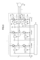
A first power semiconductor device 11 a constituting a U-phase upper arm and a second power semiconductor device 11 b constituting a U-phase lower arm are connected in series, and are connected to the direct-current capacitor 2. The first and second power semiconductor devices (11 a, 11 b) are each configured to be sealed in a casing as the so-called 1 in 1 module. A 1 in 1 module 10 a in which the first power semiconductor device 11 a is sealed has at least four terminals, specifically, a first main current drain terminal 12 a, a first main current source terminal 13 a, a first control gate terminal 14 a and a first control source terminal 15 a. A 1 in 1 module 10 b in which the second power semiconductor device 11 b is sealed has the same concept, and is provided with a second main current drain terminal 12 b, a second main current source terminal 13 b, a second control gate terminal 14 b and a second control source terminal 15 b.
A connection end 25 between the first main current source terminal 13 a of the first power semiconductor device 11 a and the second main current drain terminal 12 b of the second power semiconductor device 11 b is coupled to an induction motor 5 as a load through a U-phase output line 7. A casing of the induction motor 5 is grounded via a ground line 6 in terms of safety. The negative electrode side of the direct-current capacitor 2 is also grounded via a ground line 3.
A U-phase output inductor 20 is illustrated between the connection end 25 and the induction motor 5. The U-phase output inductor 20 may be an inductor that has an inductance component, and may be a wire-wound reactor with a core or a wire-wound reactor without a core. Alternatively, the U-phase output inductor 20 may be a parasitic inductance of the U-phase output line 7. In this case, time and effort to prepare a coil separately and connect it can be eliminated.
A first gate driving circuit 18 a is coupled to the first control gate terminal 14 a and the first control source terminal 15 a in the first power semiconductor device 11 a, and supplies an electrical charge to the first power semiconductor device 11 a to drive the first power semiconductor device 11 a.
A second gate driving circuit 19 is connected to the second control gate terminal 14 b and the second control source terminal 15 b in the second power semiconductor device 11 b, and supplies an electrical charge to the second power semiconductor device 11 b to drive the second power semiconductor device 11 b.
The first main current drain terminal 12 a of the first power semiconductor device 11 a is connected to a positive electrode of the direct-current capacitor 2. The second main current source terminal 13 b of the second power semiconductor device 11 b is connected to a negative electrode of the direct-current capacitor 2. The first power semiconductor device 11 a and the second power semiconductor device 11 b are turned on alternately to perform the so-called switching operation.
When the first power semiconductor device 11 a is on and the second power semiconductor device 11 b is off, a potential of the positive electrode of the direct-current capacitor 2 can be supplied to the induction motor 5 through the U-phase output line 7. When the first power semiconductor device 11 a is off and the second power semiconductor device 11 b is on, a potential of the negative electrode of the direct-current capacitor 2 can be supplied to the induction motor 5 through the U-phase output line 7.
By driving the power semiconductor devices in the U phase, the V phase and the W phase appropriately, the potential supplied from the power converter 1 to the induction motor 5 can be changed, and a rotation speed and a rotation torque of the induction motor 5 can be controlled.
A controller 30 generates control signals to drive the power semiconductor devices. In the U phase, for example, control signals outputted from the controller 30 are isolated by signal isolators 24 a and 24 b, and transmitted to the first gate driving circuit 18 a and the gate driving circuit 19, respectively.
Here, the reason why the signal isolators are necessary will be described. For example, the first gate driving circuit 18 a is connected to the first control source terminal 15 a of the first power semiconductor device 11 a, and the potential of the first gate driving circuit 18 a is equal to that of the first control source terminal 15 a of the first power semiconductor device 11 a.
As described above, when the first power semiconductor device 11 a is on and the second power semiconductor device 11 b is off, the first main current source terminal 13 a of the first power semiconductor device 11 a is equal in potential to the positive electrode of the direct-current capacitor 2. Thus the potential of the first gate driving circuit 18 a is approximately equal to the potential of the positive electrode of the direct-current capacitor 2. However, a control signal cannot be transmitted directly from the controller 30 to the first gate driving circuit 18 a being at a high potential. Therefore, the signal isolator 24 a for isolating the control signal is required.
On the other hand, since the second main current source terminal 13 b of the second power semiconductor device 11 b is equal in potential to the negative electrode of the direct-current capacitor 2 at all times, the potential of the gate driving circuit 19 is also approximately equal to the potential of the negative electrode of the direct-current capacitor 2. That is, unlike the first gate driving circuit 18 a, the gate driving circuit 19 is at a low potential, and thus a control signal can be directly transmitted from the controller 30.
However, due to the switching operation of the second power semiconductor device 11 b, a switching current may flow through a parasitic resistive component, and the potential of the second main current source terminal 13 b of the second power semiconductor device 11 b may fluctuate, and there may be a case where the time rate of change of the potential is significantly high. Thus, in order to prevent a malfunction of the controller 30, it is a preferable implementation mode to provide the signal isolator 24 b also for the gate driving circuit 19.
The signal isolators 24 a and 24 b, in exchange for high isolation properties, have characteristics of delaying signal transmission since they convert electrical signals from the controller 30 for shaping processing.
In the circuit in the first embodiment illustrated in FIG. 1 , the U-phase output inductor 20 and the first gate driving circuit 18 a are connected without the intervention of the signal isolator 24 a, and the first gate driving circuit 18 a monitors a voltage developed across the U-phase output inductor 20.
Typically, the number of revolutions of the induction motor 5 is about 1 Hz to 100 Hz, and at the fastest, in the order of 1 kHz or 10 kHz. Thus, a frequency of the alternating current that the power converter 1 supplies to the induction motor 5 is typically about 1 Hz to 100 Hz, and at the fastest, in the order of 1 kHz or 10 kHz. Since the time rate of change of the current is gentle, a large voltage due to an inductance component is not considered to be developed across the U-phase output inductor 20.
Next, consider a case where an isolation failure occurs in the induction motor 5, for example, and the U-phase output line 7 and the casing of the induction motor 5 suffer short-circuit faults at low impedance. At this time, a short-circuit current flows by a route of the positive electrode of the direct-current capacitor 2→the first power semiconductor device 11 a→the U-phase output inductor 20→the U-phase output line 7→the casing of the induction motor 5→the ground line 6→the ground→the ground line 3→the negative electrode of the direct-current capacitor 2. Since this type of short-circuit current increases in current value in a short period of time, it is necessary to detect a short-circuit abnormality at an early stage, and provide a turnoff instruction to the first power semiconductor device 11 a to eliminate the conduction of a short-circuit current.
In the circuit configuration in FIG. 1 , when a short-circuit fault occurs, a large voltage due to inductance is developed in the U-phase output inductor 20. The first gate driving circuit 18 a monitors the voltage developed across the U-phase output inductor 20, thereby detecting an abnormality and turning off the first power semiconductor device 11 a. The first power semiconductor device 11 a is turned off immediately when an abnormality is detected since the signal isolator 24 a having the characteristics of delaying signal transmission does not intervene. By doing so, it is possible to shorten the delay time until the conduction of a short-circuit current is eliminated. Also in the V phase and the W phase, the same circuit configuration is used. Thus as for short-circuit currents generated in the V phase and the W phase, the conduction of the short-circuit currents can be eliminated in a short period of time.
The same applies when an isolation failure occurs in the induction motor 5 and the U-phase output line 7 and the V-phase output line 8 suffer short-circuit faults at low impedance. Or the same applies when the U-phase output line 7 and the V-phase output line 8 are broken down in isolation, and suffer short-circuit faults at low impedance. In these cases, a short-circuit current flows by a route of the positive electrode of the direct-current capacitor 2→the first power semiconductor device 11 a in the U phase→the U-phase output inductor 20→the U-phase output line 7→the V-phase output line 8→a V-phase output inductor 28→a second power semiconductor device 11 b in the V phase→the negative electrode of the direct-current capacitor 2.
The first gate driving circuit 18 a in the U phase monitors the voltage developed across the U-phase output inductor 20, thereby detecting an abnormality and turning off the first power semiconductor device 11 a. A first gate driving circuit 18 a in the V phase monitors the voltage in the V-phase output inductor 28, thereby detecting an abnormality and turning off a first power semiconductor device 11 a in the V phase. The delay time since an abnormality is detected until the first power semiconductor device 11 a is turned off and the conduction of a short-circuit current is eliminated can be shortened since a signal isolator having the characteristics of delaying signal transmission does not intervene.
As is clear from the above description, the circuit configuration in the first embodiment, as long as an abnormality is a short-circuit abnormality of a short-circuit current flowing through an output reactor, can deal with occurrence of any short-circuit abnormality, and allows transmission of a signal indicating a short-circuit abnormality to be performed immediately to turn off a power semiconductor device, thereby making it possible to shorten the delay time until the conduction of a short-circuit current is eliminated.
Next, the first gate driving circuit 18 a according to the first embodiment will be described. FIG. 2 is a diagram illustrating a detailed circuit configuration of the first gate driving circuit 18 a, and also illustrates connections to a power semiconductor device and an output inductor that are peripheral circuit components. The gate driving circuit 19 is a generally used gate driving circuit for controlling the drive of the second power semiconductor device 11 b.
In the first gate driving circuit 18 a, an on capacitor 34 a is connected on the upper-level side and an off capacitor 36 a is connected on the lower-level side. A point of connection between the on capacitor 34 a and the off capacitor 36 a is connected to the first control source terminal 15 a of the first power semiconductor device 11 a. Based on a technique publicly known to those skilled in the art such a radio frequency pulse transformer or main circuit feeding, the on capacitor 34 a and the off capacitor 36 a are supplied with a charge and controlled to have a fixed voltage.
The positive electrode of the on capacitor 34 a is connected to a control gate terminal of the first power semiconductor device 11 a via an on transistor 30 a and a gate resistor 37 a. The negative electrode of the off capacitor 36 a is connected to the control gate terminal of the first power semiconductor device 11 a via an off transistor 32 a and the gate resistor 37 a. The on transistor 30 a and the off transistor 32 a are turned on alternately.
When the on transistor 30 a is turned on, a circuit is formed having a path of the positive electrode of the on capacitor 34 a→the on transistor 30 a→the gate resistor 37 a→the control gate terminal of the first power semiconductor device 11 a→the first control source terminal 15 a of the first power semiconductor device 11 a→the negative electrode of the on capacitor 34 a. This operation allows a positive bias corresponding to the voltage of the on capacitor 34 a to be applied between the first control gate terminal 14 a and the first control source terminal 15 a of the first power semiconductor device 11 a, and so the first power semiconductor device 11 a is brought into an on state.
On the other hand, when the off transistor 32 a is turned on, a circuit is formed having a path of the negative electrode of the off capacitor 36 a→the off transistor 32 a→the gate resistor 37 a→the control gate terminal of the first power semiconductor device 11 a→the first control source terminal 15 a of the first power semiconductor device 11 a→the positive electrode of the off capacitor 36 a. A negative bias corresponding to the voltage of the off capacitor 36 a can be applied between the first control gate terminal 14 a and the first control source terminal 15 a of the first power semiconductor device 11 a, and so the first power semiconductor device 11 a is brought into an off state.
The above-described configuration is one of examples of the configuration of the gate driving circuit. The examples include a configuration example where a location of the gate resistor is changed and also a configuration example in which MOSFETs are used instead of bipolar transistors. In any case, the first gate driving circuit 18 a is connected to the first control source terminal 15 a of the first power semiconductor device 11 a, and the potential of the first gate driving circuit 18 a is equal to the potential of the first control source terminal 15 a of the first power semiconductor device 11 a.
The signal isolators 24 a and 24 b are typically configured to use components called the so-called photocouplers. For example, in FIG. 2 , a primary side of the photocoupler in the signal isolator 24 a is constructed of a photodiode 24 a 1. The photodiode 24 a 1 receives an electrical signal for driving the first power semiconductor device 11 a from the controller 30. The photodiode 24 a 1 blinks to convert the electrical signal into an optical signal. The secondary side of the photocoupler is constructed of a phototransistor 24 a 2. The phototransistor 24 a 2 receives the optical signal of the photodiode 24 a 1 to switch between a state of conduction between secondary-side terminals and a state of non-conduction between the secondary-side terminals. That is, the phototransistor 24 a 2 converts the optical signal into an electrical signal. The secondary side of the signal isolator 24 a is connected to the first gate driving circuit 18 a to transmit the electrical signal to the first gate driving circuit 18 a. In this way, the photocoupler constituting the signal isolator 24 a transmits a signal while isolating the potential of the controller 30 from the potential of the first gate driving circuit 18 a by using an optical signal.
Although the signal isolator 24 a has been explained as a device using an optical signal in the above description, a device using an electric field signal may be used or a device using a magnetic signal may be used since use of a signal other than an electrical signal allows isolation.
However, the signal isolator 24 a, in exchange for high isolation properties, has characteristics of delaying signal transmission since it converts an electrical signal from the controller 30 for shaping processing thereof, as described above.
One of the main points of the present invention is that both ends of the U-phase output inductor 20 are connected to the first gate driving circuit 18 a without the intervention of the signal isolator 24 a. As described above, typically, when the power converter 1 drives the induction motor 5, a large voltage due to an inductance component is not developed across the U-phase output inductor 20. On the other hand, when a short-circuit abnormality occurs and a short-circuit current flows in a path through the U-phase output inductor 20, a voltage due to an inductance component is developed across the U-phase output inductor 20. Therefore, using the voltage developed across the U-phase output inductor 20 allows detection of a short-circuit abnormality.
By adjusting the inductance value of the U-phase output inductor 20, the magnitude of the value of the voltage generated can be adjusted. In any case, the voltage developed in the U-phase output inductor 20 is not a high voltage, and the both ends of the U-phase output inductor 20 can be connected to the first gate driving circuit 18 a without the intervention of the signal isolator 24 a.
The first gate driving circuit 18 a processes the voltage developed across the U-phase output inductor 20 by a differential amplification circuit 38 a using an operational amplifier. The larger the voltage developed across the U-phase output inductor 20 is, the larger the amount of change in the output voltage of the differential amplification circuit 38 a becomes.
A comparator 40 a receives the output voltage of the differential amplification circuit 38 a and compares it to a reference voltage. With this configuration, when the voltage developed across the U-phase output inductor 20 exceeds a preset threshold voltage, the output of the comparator 40 a changes from “High” to “Low.” The output of the comparator 40 a is connected to a transistor 33 a that drives the on transistor 30 a and the off transistor 32 a of the first gate driving circuit 18 a. When the output of the comparator 40 a changes from “High” to “Low,” the on transistor 30 a is turned off and the off transistor 32 a is turned off, irrespective of whether a signal from the controller 30 is an on instruction or an off instruction. That is, the first power semiconductor device 11 a is controlled to be off irrespective of whether the signal from the controller 30 is an on instruction or an off instruction. In this way, the first power semiconductor device 11 a can be controlled from the detection of the voltage across the U-phase output inductor 20 to the power semiconductor device without the intervention of the signal isolator 24 a having the characteristics of delaying signal transmission, so that the delay time between detection of an abnormal short-circuit and turnoff of the first power semiconductor device 11 a can be shortened.
As described above, according to the power converter in the first embodiment, in a power converter having at least one bridge circuit configured to have upper and lower arms in which a first power semiconductor device and a second power semiconductor device are connected in series, a first gate driving circuit that supplies a charge to the first power semiconductor device of the upper arm to drive the device monitors a voltage developed by an output inductor between a connection end between the first power semiconductor device and the second power semiconductor device, and a load, and performs control to protect the first power semiconductor device based on a value of the monitored voltage. By so doing, it is possible to achieve an effect of allowing a short-circuit abnormality such as the flow of an excessive short-circuit current to be detected to protect the first power semiconductor device, and allowing a delay time until the conduction of a short-circuit current is eliminated, to be made shorter.
By configuring the first gate driving circuit using a differential amplifier and inputting the voltage developed across the output inductor to the differential amplifier, a value of a current flowing through an output line can be estimated, and based on the estimated current value, the control to protect the first power semiconductor device can be performed.
The first power semiconductor device 11 a constituting a U-phase upper arm and the second power semiconductor device 11 b constituting a U-phase lower arm are connected in series, and connected to a direct-current capacitor 2. The first power semiconductor device 11 a and the second power semiconductor device 11 b are configured to be both sealed in a single casing as the so-called 2 in 1 module. A 2 in 1 module 10 c in which the first power semiconductor device 11 a and the second power semiconductor device 11 b are sealed is provided with at least seven terminals, specifically, a first main current drain terminal 12 a, a first control gate terminal 14 a, a first control source terminal 15 a, a second main current source terminal 13 b, a second control gate terminal 14 b, a second control source terminal 15 b, and a load connection terminal 13 c.
The first control source terminal 15 a of the first power semiconductor device 11 a and a connection end 25 between the first power semiconductor device 11 a and the second power semiconductor device 11 b located inside the 2 in 1 module 10 c are connected to an induction motor 5 as a load through a U-phase output line 7 connected to the load connection terminal 13 c.
A U-phase output inductor 21 is illustrated between the connection end 25 and the load connection terminal 13 c, and a first inductor 22 a is illustrated between the first control source terminal 15 a of the first power semiconductor device 11 a and the connection end 25. In this embodiment, for the U-phase output inductor 21 and the first inductor 22 a, the parasitic inductance inherent in wiring lines in the module is used. Using parasitic inductance has an advantage of eliminating the need to provide coils individually.
A first gate driving circuit 18 c is connected to the first control gate terminal 14 a and the first control source terminal 15 a in the first power semiconductor device 11 a, and supplies a charge to the first power semiconductor device 11 a to drive the first power semiconductor device 11 a.
The first gate driving circuit 18 c processes the voltage developed across the U-phase output inductor 21 and first inductor 22 a by a time integration circuit 39 a using an operational amplifier. Since the voltage developed across the U-phase output inductor 21 and first inductor 22 a represents a time rate of change in the flowing current, an output of the time integration circuit 39 a represents a value of a current flowing through both the U-phase output inductor 21 and the first inductor 22 a (flowing current value).
That is, the first gate driving circuit 18 c can know a value of a current flowing through the U-phase output inductor 21 and first inductor 22 a, and can perform abnormality determination and protection control based on the current value.
The output of the time integration circuit 39 a is inputted to a comparator 40 a. The comparator 40 a receives the output voltage of the time integration circuit 39 a, and compares it to a reference voltage. An operation after that is the same as that in the first embodiment illustrated in FIG. 2 . Specifically, when a short-circuit abnormality is detected based on the voltage across the U-phase output inductor 21 and first inductor 22 a, the first power semiconductor device 11 a is controlled to be off irrespective of whether a signal from the controller 30 is an on instruction or an off instruction.
As described above, according to the power converter of the second embodiment, in a power converter having at least one bridge circuit configured to have upper and lower arms in which a first power semiconductor device and a second power semiconductor device are connected in series, a first gate driving circuit that supplies a charge to the first power semiconductor device of an upper arm to drive the device monitors a third voltage representing a total value of a first voltage developed by a first inductor between a connection end between the first power semiconductor device and the second power semiconductor device, and a first main current source terminal, and a second voltage developed by an output inductor between the connection end and a load, and performs control to protect the first power semiconductor device based on a value of the monitored voltage. Accordingly, an advantageous effect is exerted in which a short-circuit abnormality such as the flow of an excessive short-circuit current can be detected to protect the first power semiconductor device, and a delay time until the conduction of a short-circuit current is eliminated can be made shorter.
Although the third voltage representing the total value of the first voltage developed by the first inductor and the second voltage developed by the output inductor is monitored in the second embodiment as described above, the first voltage and the second voltage may be monitored separately. Compared to the case where the third voltage representing the total value of the first voltage and the second voltage is monitored, there is a disadvantage of increased connections to the first gate driving circuit, but by monitoring the first voltage and the second voltage separately, their respective voltage values can be checked and evaluated separately, providing an advantage of facilitating distinction among short-circuit abnormality situations.
It is preferable to time-integrate the third voltage representing the total value of the first voltage developed by the first inductor and the second voltage developed by the output inductor. The time-integration of the third voltage representing a dI/dt component allows estimation of a value of the current, thus providing an advantage of allowing protection focusing on the current value.
Further, in the power converter according to the second embodiment, the first voltage developed at the first inductor between the first power semiconductor device and the second power semiconductor device is used to determine a short-circuit abnormality, thus allowing detection of even a short-circuit abnormality by which a short-circuit current flows between the first power semiconductor device and the second power semiconductor device.
Furthermore, the power converter according to the second embodiment has an advantage of eliminating the need to provide an output reactor separately since the inherent parasitic inductance of the wiring line inside the casing can be used. This implementation form can be easily and simply realized by using a 2 in 1 module.
Although FIG. 3 illustrates connections in a 2 in 1 module, the same wiring is also possible in a 1 in 1 module. In a 1 in 1 module, a parasitic inductance of wiring lines outside a casing thereof can be used.
Although the second embodiment illustrates the implementation form of using the parasitic inductance of the wiring lines inside the casing as the U-phase output inductor 21, instead of inputting the potential at the load connection terminal 13 c to the first gate driving circuit 18 c, input may be made from any point on the U-phase output wiring line 7 closer to the load side than the load connection terminal 13 c. In this case, as the U-phase output inductor 21, not only a parasitic inductance component of internal wiring lines but also a parasitic inductance component of external wiring lines can be used, thus providing an advantageous effect of making is possible to increase the voltage developed at a detected part.
As the U-phase output inductor 21, in place of the parasitic inductance components of internal wiring lines and external wiring lines, or in place of the parasitic inductance component of external wiring lines, a substantial output reactor such as a wire-wound reactor may be used. Using a substantial wire-wound reactor can increase a value of a voltage generated, providing an advantageous effect of facilitating design of the first gate driving circuit.
The first gate driving circuit 18 c processes the voltage developed across the U-phase output inductor 21 and first inductor 22 a by a time integration circuit 39 a using an operational amplifier. Since the voltage developed across the U-phase output inductor 21 and first inductor 22 a represents the time rate of change in flowing current, the output of the time integration circuit 39 a represents the value of a current flowing through both the U-phase output inductor 21 and the first inductor 22 a (flowing current value).
That is, the first gate driving circuit 18 c can know the value of the current flowing through the U-phase output inductor 21 and first inductor 22 a, and can perform abnormality determination and protection control based on the current value.
The second gate driving circuit 18 d processes the voltage developed across the second inductor 22 b by a time integration circuit 39 b using an operational amplifier. Since the voltage developed across the second inductor 22 b represents a time rate of change in a flowing current, an output of the time integration circuit 39 b represents a value of a current flowing through the second inductor 22 b (flowing current value).
That is, the second gate driving circuit 18 d can know the flowing current value of the second inductor 22 b, and can perform abnormality determination and protection control based on the current value.
In the configuration of the third embodiment, a difference between the inductance value of the first inductor 22 a and the inductance value of the second inductor 22 b is preferably 20% or less. The reason is as follows.
Approximate variations of components typically used in a gate driving circuit are 20% for electrolytic capacitors, 10% for ceramic capacitors, and 5% for resistors. Therefore, designing using the variation value of the electrolytic capacitors having the largest numerical value as the range of variations of the inductance value of the first inductor 22 a and the inductance value of the second inductor 22 b can communalize the component values between the first gate driving circuit 18 c and the second gate driving circuit 18 d. When the component values can be communalized, a circuit can be built up without selecting specific components, so that component management is facilitated, resulting in an advantageous effect of allowing reductions in component management and manufacturing cost.
As described above, according to the power converter according to the third embodiment, in a power converter having at least one bridge circuit configured to have upper and lower arms in which a first power semiconductor device and a second power semiconductor device are connected in series, a first gate driving circuit that supplies a charge to the first power semiconductor device of an upper arm to drive the device monitors a third voltage representing a total value of a first voltage developed by a first inductor located on a path of a current flowing through the first power semiconductor device, and a second voltage developed by an output inductor between a connection end between the first power semiconductor device and the second power semiconductor device, and a load, and performs control to protect the first power semiconductor device based on a value of the monitored voltage, while a second gate driving circuit that supplies a charge to the second power semiconductor device of a lower arm to drive the device monitors a fourth voltage developed by a second inductor located on a path of a current flowing through the second power semiconductor device, and performs control to protect the second power semiconductor device based on a value of the monitored voltage. Accordingly, an advantageous effect is exerted in which a short-circuit abnormality such as the flow of an excessive short-circuit current can be detected to protect the first and second power semiconductor devices, and a delay time until the conduction of a short-circuit current is eliminated can be made shorter.
It is preferable that the fourth voltage developed by the second inductor be time-integrated. By time-integrating the fourth voltage representing a dI/dt component, a value of the current can be estimated, thus resulting in an effect of allowing protection focusing on the current value.
Further, in the power converter according to the third embodiment, the first voltage developed by the first inductor located on the path of a current flowing through the first power semiconductor device and the fourth voltage developed by the second inductor located on the path of a current flowing through the second power semiconductor device are used for the determination of a short-circuit abnormality, so that it is possible to detect even a short-circuit abnormality in which a short-circuit current flows through the first power semiconductor device but does not flow through the second power semiconductor device, and on the other hand a short-circuit abnormality in which a short-circuit current flows through the second power semiconductor device but does not flow through the first power semiconductor device.
In the first to third embodiments, applications to a power converter with three-phase two-level circuits have been illustrated. In a fourth embodiment, applications to a power converter with three-phase three-level circuits will be described with reference to FIGS. 7 and 8 . FIG. 7 is a diagram illustrating a configuration example of an application to a power converter with a clamping diode type three-phase three-level circuit. FIG. 8 is a diagram illustrating a configuration example of an application to a power converter with a synchronous rectification type three-phase three-level circuit. The configurations of the clamping diode type three-phase three-level circuit and the synchronous rectification type three-phase three-level circuit are publicly known, and therefore will not be described. As with the case of the three-phase two-level, the configurations of the three phases are identical or equivalent. Thus the following description focuses on a U phase for explanation.
In FIG. 7 , an upper-level side first power semiconductor device 11 a 1, a lower-level side first power semiconductor device 11 a 2 and an upper-level side clamping diode 26 a constitute an upper arm, and an upper-level side second power semiconductor device 11 b 1, a lower-level side second power semiconductor device 11 b 2 and a lower-level side clamping diode 26 b constitute a lower arm. A connection end between the lower-level side first power semiconductor device 11 a 2 and the upper-level side second power semiconductor device 11 b 1 is a connection end 25, a connection end between the upper-level side first power semiconductor device 11 a 1 and the lower-level side first power semiconductor device 11 a 2 is a connection end 25 a, and a connection end between the upper-level side second power semiconductor device 11 b 1 and the lower-level side second power semiconductor device 11 b 2 is a connection end 25 b.
An upper-level side first inductor 22 a 1 is illustrated between the upper-level side first power semiconductor device 11 a 1 and the lower-level side first power semiconductor device 11 a 2, a lower-level side first inductor 22 a 2 is illustrated between the connection end 25 and the lower-level side first power semiconductor device 11 a 2, an upper-level side second inductor 22 b 1 is illustrated between the upper-level side second power semiconductor device 11 b 1 and the lower-level side second power semiconductor device 11 b 2, and a lower-level side second inductor 22 b 2 is illustrated between the lower-level side second power semiconductor device 11 b 2 and the negative electrode of a direct-current capacitor 2 b.
A U-phase output inductor 21 a 2 is illustrated between the connection end 25 and the induction motor 5, an upper-level side third inductor 21 a 1 is illustrated between the connection end 25 a and a cathode of the upper-level side clamping diode 26 a, and a lower-level side third inductor 21 b 1 is illustrated between the connection end 25 b and an anode of the lower-level side clamping diode 26 b.
In this embodiment, as the upper-level side first inductor 22 a 1, the lower-level side first inductor 22 a 2, the upper-level side second inductor 22 b 1, the lower-level side second inductor 22 b 2, the U-phase output inductor 21 a 2, the upper-level side third inductor 21 a 1, and the lower-level side third inductor 21 b 1, parasitic inductances inherent in in-module wiring lines or out-of-module wiring lines are used. The use of the parasitic inductances has an advantage in that coils are not required to be provided individually.
A first gate driving circuit 18 a 1 is connected to a first control gate terminal and a first control source terminal in the upper-level side first power semiconductor device 11 a 1, and supplies a charge to the upper-level side first power semiconductor device 11 a 1 to drive the upper-level side first power semiconductor device 11 a 1. Another first gate driving circuit 18 a 2 is connected to a first control gate terminal and a first control source terminal in the lower-level side first power semiconductor device 11 a 2, and supplies a charge to the lower-level side first power semiconductor device 11 a 2 to drive the lower-level side first power semiconductor device 11 a 2. A second gate driving circuit 18 b 1 is connected to a second control gate terminal and a second control source terminal in the upper-level side second power semiconductor device 11 b 1, and supplies a charge to the upper-level side second power semiconductor device 11 b 1 to drive the upper-level side second power semiconductor device 11 b 1. A second gate driving circuit 18 b 2 is connected to a second control gate terminal and a second control source terminal in the lower-level side second power semiconductor device 11 b 2, and supplies a charge to the lower-level side second power semiconductor device 11 b 2 to drive the lower-level side second power semiconductor device 11 b 2.
Voltage developed across the upper-level side first inductor 22 a 1 and upper-level side third inductor 21 a 1 is inputted to the first gate driving circuit 18 a 1. The circuit configuration of the first gate driving circuit 18 a 1 is identical or equivalent to that of the first gate driving circuit 18 c illustrated in FIG. 4 or FIG. 6 . By processing the voltage developed across the upper-level side first inductor 22 a 1 and upper-level side third inductor 21 a 1 by the time integration circuit 39 a using an operational amplifier, a value of a current flowing through the upper-level side first inductor 22 a 1 and the upper-level side third inductor 21 a 1 (flowing current value) can be grasped, and abnormal determination and protection control based on the current value can be performed.
The first gate driving circuit 18 a 2, the second gate driving circuit 18 b 1 and the second gate driving circuit 18 b 2 operate in the same manner, and will not be described.
On the power converter with the synchronous rectification type three-phase three-level circuit, basic concept is the same. In the power converter with the synchronous rectification type three-phase three-level circuit, as illustrated in FIG. 8 , an upper-level side third power semiconductor device 11 a 3 is provided in place of the upper-level side clamping diode 26 a, and a lower-level side third power semiconductor device 11 b 3 is provided in place of the lower-level side clamping diode 26 b.
When a connection end between the upper-level side third power semiconductor device 11 a 3 and the lower-level side third power semiconductor device 11 b 3 is a connection end 25 c, an upper-level side third inductor 22 a 3 is illustrated between the connection end 25 c and the upper-level side third power semiconductor device 11 a 3, a lower-level side third inductor 22 b 3 is illustrated between an end of the third inductor 21 b 1 and the lower-level side third power semiconductor device 11 b 3, and a U-phase input inductor 21 a 3 is illustrated between the connection end 25 c and the positive electrode of a direct-current capacitor 2 b (the negative electrode of 2 a).
As the upper-level side third inductor 22 a 3, the lower-level side third inductor 22 b 3 and the U-phase input inductor 21 a 3, parasitic inductances inherent in in-module wiring lines or out-of-module wiring lines are used. The use of the parasitic inductances has an advantage in that coils are not required to be provided individually.
A third gate driving circuit 18 a 3 is connected to a third control gate terminal and a third control source terminal in the upper-level side third power semiconductor device 11 a 3, and supplies a charge to the upper-level side third power semiconductor device 11 a 3 to drive the upper-level side third power semiconductor device 11 a 3. A fourth gate driving circuit 18 b 3 is connected to a third control gate terminal and a third control source terminal in the lower-level side third power semiconductor device 11 b 3, and supplies a charge to the lower-level side third power semiconductor device 11 b 3 to drive the lower-level side third power semiconductor device 11 b 3.
A voltage developed across the upper-level side third inductor 22 a 3 and U-phase input inductor 21 a 3 is inputted to the third gate driving circuit 18 a 3. A voltage developed across the lower-level side third inductor 22 b 3 is inputted to the fourth gate driving circuit 18 b 3. The circuit configurations of the third gate driving circuit 18 a 3 and the fourth gate driving circuit 18 b 3 are identical or equivalent to that of the first gate driving circuit 18 c illustrated in FIG. 4 or FIG. 6 .
In the third gate driving circuit 18 a 3, by processing a voltage developed across the upper-level side third inductor 22 a 3 and the U-phase input inductor 21 a 3 by the time integration circuit 39 a using an operational amplifier, a value of a current flowing through the upper-level side third inductor 22 a 3 and the U-phase input inductor 21 a 3 (flowing current value) can be grasped, and abnormal determination and protection control based on the current value can be performed.
In the fourth gate driving circuit 18 b 3, by processing a voltage developed across the lower-level side third inductor 22 b 3 by the time integration circuit 39 a using an operational amplifier, a value of a current flowing through the lower-level side third inductor 22 b 3 (flowing current value) can be grasped, and abnormal determination and protection control based on the current value can be performed.
The configurations illustrated in the above first to fourth embodiments are examples of the configuration of the present invention, and may be combined with another known technique, or may be configured with a change such as an omission of a part without departing from the scope of the present invention as a matter of course.
As above, the present invention is useful for a power converter capable of detecting short-circuit abnormality and protecting power semiconductor devices.
1 power converter, 2, 2 a, 2 b direct-current capacitor, 3, 6 ground line, 5 induction motor, 7 U-phase output line, 8 V-phase output line, 10 a, 10 b 1 in 1 module, 10 c 2 in 1 module, 11 a first power semiconductor device, 11 a 1 upper-level side first power semiconductor device, 11 a 2 lower-level side first power semiconductor device, 11 a 3 upper-level side third power semiconductor device, 11 b second power semiconductor device, 11 b 1 upper-level side second power semiconductor device, 11 b 2 lower-level side second power semiconductor device, 11 b 3 lower-level side third power semiconductor device, 12 a first main current drain terminal, 12 b second main current drain terminal, 13 a first main current source terminal, 13 b second main current source terminal, 13 c load connection terminal, 14 a first control gate terminal, 14 b second control gate terminal, 15 a first control source terminal, 15 b second control source terminal, 18 a, 18 a 1, 18 a 2, 18 c, 18 d first gate driving circuit, 18 b 1, 18 b 2, 18 d second gate driving circuit, 18 a 3 third gate driving circuit, 18 b 3 fourth gate driving circuit, 19 gate driving circuit, 20, 21, 21 a 2 U-phase output inductor, 21 a 1 upper-level side third inductor, 21 b 1 lower-level side third inductor, 21 a 3 U-phase input inductor, 22 a first inductor, 22 b second inductor, 22 a 1 upper-level side first inductor, 22 a 2 lower-level side first inductor, 22 b 1 upper-level side second inductor, 22 b 2 lower-level side second inductor, 22 a 3 upper-level side third inductor, 22 b 3 lower-level side third inductor, 24 a, 24 b signal isolator, 25, 25 a, 25 b, 25 c connection end, 26 a upper-level side clamping diode, 26 b lower-level side clamping diode, 28 V-phase output inductor, 30 controller, 30 a on transistor, 32 a off transistor, 33 a transistor, 34 a on capacitor, 36 a off capacitor, 37 a gate resistor, 38 a differential amplification circuit, 39 a time integration circuit, 39 b time integration circuit, 40 a comparator, 24 a 1 photodiode, 24 a 2 phototransistor
Claims (15)
1. A power converter including at least one bridge circuit configured to have upper and lower arms in which a first power semiconductor device and a second power semiconductor device are connected in series, the power converter comprising:
a first gate driving circuit connected to a first control gate terminal and a first control source terminal in the first power semiconductor device, to supply a charge to the first power semiconductor device to drive the first power semiconductor device; and
a second gate driving circuit connected to a second control gate terminal and a second control source terminal in the second power semiconductor device, to supply a charge to the second power semiconductor device to drive the second power semiconductor device, wherein
a first main current source terminal of the first power semiconductor device is connected to a second main current drain terminal of the second power semiconductor device, and an end of the connection is connected to a load by an output line, and
the first gate driving circuit monitors a first voltage developed by an output inductor between the connection end and the load, and performs control to protect the first power semiconductor device based on a value of the monitored voltage.
2. The power converter according to claim 1 , wherein the first gate driving circuit includes a differential amplifier, estimates a value of a current flowing through the output line based on the first voltage, and performs control to protect the first power semiconductor device based on the estimated current value.
3. The power converter according to claim 1 , wherein the first power semiconductor device and the second power semiconductor device are sealed in different casings, respectively, and the output inductor is a parasitic inductance of the output line.
4. The power converter according to claim 1 , wherein the first power semiconductor device and the second power semiconductor device are sealed in a single casing, and the output inductor is a parasitic inductance obtained by a line inside the casing.
5. The power converter according to claim 1 , wherein the first power semiconductor device and the second power semiconductor device are sealed in a single casing, and the output inductor is a parasitic inductance of an output line disposed outside the casing.
6. The power converter according to claim 1 , wherein the first power semiconductor device and the second power semiconductor device are sealed in a single casing, and the output inductor is a combined inductance component of a parasitic inductance obtained by an output line inside the casing and a parasitic inductance of an output line disposed outside the casing.
7. A power converter including at least one bridge circuit configured to have upper and lower arms in which a first power semiconductor device and a second power semiconductor device are connected in series, the power converter comprising:
a first gate driving circuit connected to a first control gate terminal and a first control source terminal in the first power semiconductor device, to supply a charge to the first power semiconductor device to drive the first power semiconductor device; and
a second gate driving circuit connected to a second control gate terminal and a second control source terminal in the second power semiconductor device, to supply a charge to the second power semiconductor device to drive the second power conductor device, wherein
a first main current source terminal of the first power semiconductor device is connected to a second main current drain terminal of the second power semiconductor device, and an end of the connection is connected to a load by an output line, and
the first gate driving circuit monitors a first voltage developed by a first inductor between the first main current source terminal and the connection end and a second voltage developed by an output inductor between the connection end and the load, and performs control to protect the first power semiconductor device based on respective values of the monitored voltages.
8. The power converter according to claim 7 , wherein the first gate driving circuit monitors a third voltage representing a total value of the first voltage and the second voltage, and performs control to protect the first power semiconductor device based on a value of the monitored voltage.
9. The power converter according to claim 8 , wherein the first gate driving circuit includes an integrator, estimates a value of a current flowing through the first main current source terminal by time-integrating the third voltage, and performs control to protect the first power semiconductor device based on the estimated current value.
10. The power converter according to claim 7 , wherein the second gate driving circuit monitors a fourth voltage developed by a second inductor between the second control source terminal and a second main current source terminal, and performs control to protect the second power semiconductor device based on a value of the monitored voltage.
11. The power converter according to claim 10 , wherein the second gate driving circuit includes an integrator, estimates a value of a current flowing through the second main current source terminal by time-integrating the fourth voltage, and performs control to protect the second power semiconductor device based on the estimated current value.
12. The power converter according to claim 10 , wherein a difference in inductance value between the first inductor and the second inductor is 20% or less.
13. The power converter according to claim 10 , wherein
the first power semiconductor device is sealed in a casing and the second power semiconductor device is sealed in another different casing, and
the first inductor is a parasitic inductance obtained by a line inside the casing, the second inductor is a parasitic inductance obtained by a line inside the casing, and the output inductor is a parasitic inductance of the output line.
14. The power converter according to claim 10 , wherein
the first power semiconductor device and the second power semiconductor device are sealed in a single casing, and
the first inductor, the second inductor, and the output inductor are a parasitic inductance obtained by a line inside the casing.
15. The power converter according to claim 10 , wherein
the first power semiconductor device and the second power semiconductor device are sealed in a single casing, and
the first inductor and the second inductor are a parasitic inductance obtained by a line inside the casing, and the output inductor is a combined inductance component of a parasitic inductance obtained by a line inside the casing and a parasitic inductance of the output line.
Applications Claiming Priority (1)
| Application Number | Priority Date | Filing Date | Title |
|---|---|---|---|
| PCT/JP2014/053220 WO2015121931A1 (en) | 2014-02-12 | 2014-02-12 | Power conversion apparatus |
Publications (2)
| Publication Number | Publication Date |
|---|---|
| US20170005570A1 US20170005570A1 (en) | 2017-01-05 |
| US9712044B2 true US9712044B2 (en) | 2017-07-18 |
Family
ID=53799700
Family Applications (1)
| Application Number | Title | Priority Date | Filing Date |
|---|---|---|---|
| US15/109,070 Active US9712044B2 (en) | 2014-02-12 | 2014-02-12 | Power converter |
Country Status (4)
| Country | Link |
|---|---|
| US (1) | US9712044B2 (en) |
| JP (1) | JP6099776B2 (en) |
| DE (1) | DE112014006358T5 (en) |
| WO (1) | WO2015121931A1 (en) |
Families Citing this family (9)
| Publication number | Priority date | Publication date | Assignee | Title |
|---|---|---|---|---|
| DE112016006497T5 (en) * | 2016-02-26 | 2019-02-28 | Vacon Oy | An electronic converter and a method of controlling this |
| FR3083394B1 (en) * | 2018-06-29 | 2021-03-19 | Valeo Equip Electr Moteur | POWER COMPONENT PROTECTION DEVICE FOR A TRANSISTOR BRIDGE |
| CN111527684B (en) * | 2018-07-17 | 2023-09-22 | 富士电机株式会社 | Power module with built-in driving circuit |
| EP3694090B1 (en) * | 2019-02-07 | 2022-09-28 | Mitsubishi Electric R & D Centre Europe B.V. | A method and a system for protecting at least two power semiconductors of a half bridge converter |
| EP3700038B1 (en) | 2019-02-22 | 2022-09-07 | Future Systems Besitz GmbH | An apparatus for switching and protection of a load |
| DE102019203902A1 (en) * | 2019-03-21 | 2020-09-24 | Robert Bosch Gmbh | Power transistor arrangement |
| FR3115465A1 (en) * | 2020-10-23 | 2022-04-29 | Eove | System for controlling the motorized micro-blower of a respiratory assistance device |
| JP7301243B2 (en) * | 2020-12-24 | 2023-06-30 | 三菱電機株式会社 | Gate drive circuit and power converter |
| CN116057691A (en) | 2021-02-12 | 2023-05-02 | 富士电机株式会社 | Semiconductor module |
Citations (6)
| Publication number | Priority date | Publication date | Assignee | Title |
|---|---|---|---|---|
| JPH05207766A (en) | 1992-01-23 | 1993-08-13 | Mitsubishi Electric Corp | Method and device for overcurrent protection and overcurrent detector |
| JPH11220884A (en) | 1998-02-03 | 1999-08-10 | Hitachi Ltd | Protection device of self-excitation type converter, control device of variable speed generation generator, and control device of self-quenching-type converter |
| US6304472B1 (en) * | 1999-05-14 | 2001-10-16 | Hitachi, Ltd. | Electric power converting system with integrator providing output indicative of current |
| JP2005033678A (en) | 2003-07-10 | 2005-02-03 | Yaskawa Electric Corp | Gate drive circuit |
| US8891262B2 (en) * | 2011-03-24 | 2014-11-18 | Polar Semiconductor, Llc | Series switch bridgeless power supply |
| US9197126B2 (en) * | 2009-04-01 | 2015-11-24 | Mitsubishi Electric Corporation | Power converting apparatus |
Family Cites Families (1)
| Publication number | Priority date | Publication date | Assignee | Title |
|---|---|---|---|---|
| JP2007259533A (en) * | 2006-03-22 | 2007-10-04 | Hitachi Ltd | Protective circuit for semiconductor element |
-
2014
- 2014-02-12 DE DE112014006358.4T patent/DE112014006358T5/en active Pending
- 2014-02-12 WO PCT/JP2014/053220 patent/WO2015121931A1/en active Application Filing
- 2014-02-12 US US15/109,070 patent/US9712044B2/en active Active
- 2014-02-12 JP JP2015562592A patent/JP6099776B2/en active Active
Patent Citations (8)
| Publication number | Priority date | Publication date | Assignee | Title |
|---|---|---|---|---|
| JPH05207766A (en) | 1992-01-23 | 1993-08-13 | Mitsubishi Electric Corp | Method and device for overcurrent protection and overcurrent detector |
| US5375028A (en) * | 1992-01-23 | 1994-12-20 | Mitsubishi Denki Kabushiki Kaisha | Overcurrent protective device and device for detecting overcurrent |
| JPH11220884A (en) | 1998-02-03 | 1999-08-10 | Hitachi Ltd | Protection device of self-excitation type converter, control device of variable speed generation generator, and control device of self-quenching-type converter |
| US6304472B1 (en) * | 1999-05-14 | 2001-10-16 | Hitachi, Ltd. | Electric power converting system with integrator providing output indicative of current |
| JP3454186B2 (en) | 1999-05-14 | 2003-10-06 | 株式会社日立製作所 | Power converter |
| JP2005033678A (en) | 2003-07-10 | 2005-02-03 | Yaskawa Electric Corp | Gate drive circuit |
| US9197126B2 (en) * | 2009-04-01 | 2015-11-24 | Mitsubishi Electric Corporation | Power converting apparatus |
| US8891262B2 (en) * | 2011-03-24 | 2014-11-18 | Polar Semiconductor, Llc | Series switch bridgeless power supply |
Non-Patent Citations (2)
| Title |
|---|
| International Search Report (PCT/ISA/210) issued on May 13, 2014, by the Japanese Patent Office as the International Searching Authority for International Application No. PCT/JP2014/053220. |
| Written Opinion (PCT/ISA/237) issued on May 13, 2014, by the Japanese Patent Office as the International Searching Authority for International Application No. PCT/JP2014/053220. |
Also Published As
| Publication number | Publication date |
|---|---|
| WO2015121931A1 (en) | 2015-08-20 |
| DE112014006358T5 (en) | 2016-10-20 |
| US20170005570A1 (en) | 2017-01-05 |
| JP6099776B2 (en) | 2017-03-22 |
| JPWO2015121931A1 (en) | 2017-03-30 |
Similar Documents
| Publication | Publication Date | Title |
|---|---|---|
| US9712044B2 (en) | Power converter | |
| KR102243467B1 (en) | Inverter for an electric automobile | |
| CA2903362C (en) | Power conversion device | |
| JP5146555B2 (en) | Switching element drive circuit | |
| JP6183460B2 (en) | Inverter device | |
| JP6848183B2 (en) | Current detector and semiconductor device | |
| US9024564B2 (en) | Drive control device and drive control method | |
| US9768607B2 (en) | System and method for a multi-phase snubber circuit | |
| JP2014117112A (en) | Semiconductor control device, and power conversion equipment | |
| JP2015032984A (en) | Device for driving semiconductor element, and power conversion device using the same | |
| JP6685477B1 (en) | Power conversion device and power conversion system | |
| US8963524B2 (en) | Drive circuit for switching elements | |
| JP2008067566A (en) | Three-level inverter system | |
| JP4835930B2 (en) | Inverter device provided with ground fault detection means | |
| JP2015042044A (en) | Voltage type multilevel converter | |
| CA2855496C (en) | Method for eliminating an arc driven by means of at least one phase voltage source of a converter circuit | |
| JP6246400B2 (en) | Power converter drive circuit | |
| JP6239024B2 (en) | Power converter | |
| JP2018061301A (en) | Semiconductor driving device and power conversion equipment using the same | |
| JP6751033B2 (en) | Parallel inverter device | |
| JP2021065039A (en) | Switch drive device | |
| JP2007151358A (en) | Dc voltage step-down circuit and electric power conversion system | |
| JP7373424B2 (en) | power converter | |
| US20110157948A1 (en) | Current source inverter | |
| US11949341B2 (en) | Power converter and electric motor braking method |
Legal Events
| Date | Code | Title | Description |
|---|---|---|---|
| AS | Assignment |
Owner name: MITSUBISHI ELECTRIC CORPORATION, JAPAN Free format text: ASSIGNMENT OF ASSIGNORS INTEREST;ASSIGNORS:NAKASHIMA, YUKIO;MIKI, TAKAYOSHI;REEL/FRAME:039045/0747 Effective date: 20160517 |
|
| STCF | Information on status: patent grant |
Free format text: PATENTED CASE |
|
| MAFP | Maintenance fee payment |
Free format text: PAYMENT OF MAINTENANCE FEE, 4TH YEAR, LARGE ENTITY (ORIGINAL EVENT CODE: M1551); ENTITY STATUS OF PATENT OWNER: LARGE ENTITY Year of fee payment: 4 |