US9741850B1 - Semiconductor device and method for forming the same - Google Patents
Semiconductor device and method for forming the same Download PDFInfo
- Publication number
- US9741850B1 US9741850B1 US15/235,320 US201615235320A US9741850B1 US 9741850 B1 US9741850 B1 US 9741850B1 US 201615235320 A US201615235320 A US 201615235320A US 9741850 B1 US9741850 B1 US 9741850B1
- Authority
- US
- United States
- Prior art keywords
- gate electrode
- drain
- semiconductor device
- dielectric layer
- substrate
- Prior art date
- Legal status (The legal status is an assumption and is not a legal conclusion. Google has not performed a legal analysis and makes no representation as to the accuracy of the status listed.)
- Active
Links
- 239000004065 semiconductor Substances 0.000 title claims abstract description 62
- 238000000034 method Methods 0.000 title claims description 43
- 239000000758 substrate Substances 0.000 claims abstract description 50
- 229910052751 metal Inorganic materials 0.000 claims description 22
- 239000002184 metal Substances 0.000 claims description 22
- 230000008569 process Effects 0.000 claims description 22
- 238000002955 isolation Methods 0.000 claims description 12
- 229910021332 silicide Inorganic materials 0.000 claims description 12
- FVBUAEGBCNSCDD-UHFFFAOYSA-N silicide(4-) Chemical compound [Si-4] FVBUAEGBCNSCDD-UHFFFAOYSA-N 0.000 claims description 12
- 230000001590 oxidative effect Effects 0.000 claims description 2
- 229910021420 polycrystalline silicon Inorganic materials 0.000 claims description 2
- 229920005591 polysilicon Polymers 0.000 claims description 2
- 239000010410 layer Substances 0.000 description 111
- 239000000463 material Substances 0.000 description 20
- 125000006850 spacer group Chemical group 0.000 description 9
- 230000004888 barrier function Effects 0.000 description 7
- 230000015572 biosynthetic process Effects 0.000 description 7
- 238000002513 implantation Methods 0.000 description 7
- 230000015556 catabolic process Effects 0.000 description 6
- 238000005530 etching Methods 0.000 description 6
- 239000000126 substance Substances 0.000 description 6
- 230000000694 effects Effects 0.000 description 5
- VYPSYNLAJGMNEJ-UHFFFAOYSA-N Silicium dioxide Chemical compound O=[Si]=O VYPSYNLAJGMNEJ-UHFFFAOYSA-N 0.000 description 4
- 239000011229 interlayer Substances 0.000 description 4
- 238000001459 lithography Methods 0.000 description 4
- 230000003247 decreasing effect Effects 0.000 description 3
- 239000002019 doping agent Substances 0.000 description 3
- 239000007943 implant Substances 0.000 description 3
- 238000010297 mechanical methods and process Methods 0.000 description 3
- 230000005226 mechanical processes and functions Effects 0.000 description 3
- 238000007517 polishing process Methods 0.000 description 3
- RYGMFSIKBFXOCR-UHFFFAOYSA-N Copper Chemical compound [Cu] RYGMFSIKBFXOCR-UHFFFAOYSA-N 0.000 description 2
- 229910052581 Si3N4 Inorganic materials 0.000 description 2
- NRTOMJZYCJJWKI-UHFFFAOYSA-N Titanium nitride Chemical compound [Ti]#N NRTOMJZYCJJWKI-UHFFFAOYSA-N 0.000 description 2
- RVSGESPTHDDNTH-UHFFFAOYSA-N alumane;tantalum Chemical compound [AlH3].[Ta] RVSGESPTHDDNTH-UHFFFAOYSA-N 0.000 description 2
- UQZIWOQVLUASCR-UHFFFAOYSA-N alumane;titanium Chemical compound [AlH3].[Ti] UQZIWOQVLUASCR-UHFFFAOYSA-N 0.000 description 2
- 230000008901 benefit Effects 0.000 description 2
- 230000000903 blocking effect Effects 0.000 description 2
- 238000004140 cleaning Methods 0.000 description 2
- 229910052802 copper Inorganic materials 0.000 description 2
- 239000010949 copper Substances 0.000 description 2
- 230000005684 electric field Effects 0.000 description 2
- 238000004519 manufacturing process Methods 0.000 description 2
- 229910044991 metal oxide Inorganic materials 0.000 description 2
- 150000004706 metal oxides Chemical class 0.000 description 2
- NFFIWVVINABMKP-UHFFFAOYSA-N methylidynetantalum Chemical compound [Ta]#C NFFIWVVINABMKP-UHFFFAOYSA-N 0.000 description 2
- 229910021421 monocrystalline silicon Inorganic materials 0.000 description 2
- 239000000377 silicon dioxide Substances 0.000 description 2
- HQVNEWCFYHHQES-UHFFFAOYSA-N silicon nitride Chemical compound N12[Si]34N5[Si]62N3[Si]51N64 HQVNEWCFYHHQES-UHFFFAOYSA-N 0.000 description 2
- 229910003468 tantalcarbide Inorganic materials 0.000 description 2
- MZLGASXMSKOWSE-UHFFFAOYSA-N tantalum nitride Chemical compound [Ta]#N MZLGASXMSKOWSE-UHFFFAOYSA-N 0.000 description 2
- MTPVUVINMAGMJL-UHFFFAOYSA-N trimethyl(1,1,2,2,2-pentafluoroethyl)silane Chemical compound C[Si](C)(C)C(F)(F)C(F)(F)F MTPVUVINMAGMJL-UHFFFAOYSA-N 0.000 description 2
- XUIMIQQOPSSXEZ-UHFFFAOYSA-N Silicon Chemical compound [Si] XUIMIQQOPSSXEZ-UHFFFAOYSA-N 0.000 description 1
- 230000002411 adverse Effects 0.000 description 1
- VYBYZVVRYQDCGQ-UHFFFAOYSA-N alumane;hafnium Chemical compound [AlH3].[Hf] VYBYZVVRYQDCGQ-UHFFFAOYSA-N 0.000 description 1
- UTSDGYKWHMMTDM-UHFFFAOYSA-N alumane;tungsten Chemical compound [AlH3].[W] UTSDGYKWHMMTDM-UHFFFAOYSA-N 0.000 description 1
- DNXNYEBMOSARMM-UHFFFAOYSA-N alumane;zirconium Chemical compound [AlH3].[Zr] DNXNYEBMOSARMM-UHFFFAOYSA-N 0.000 description 1
- 229910052782 aluminium Inorganic materials 0.000 description 1
- XAGFODPZIPBFFR-UHFFFAOYSA-N aluminium Chemical compound [Al] XAGFODPZIPBFFR-UHFFFAOYSA-N 0.000 description 1
- VQYHBXLHGKQYOY-UHFFFAOYSA-N aluminum oxygen(2-) titanium(4+) Chemical compound [O-2].[Al+3].[Ti+4] VQYHBXLHGKQYOY-UHFFFAOYSA-N 0.000 description 1
- 229910021417 amorphous silicon Inorganic materials 0.000 description 1
- 238000000137 annealing Methods 0.000 description 1
- 230000001010 compromised effect Effects 0.000 description 1
- 230000007547 defect Effects 0.000 description 1
- 238000005137 deposition process Methods 0.000 description 1
- 238000001312 dry etching Methods 0.000 description 1
- 230000002708 enhancing effect Effects 0.000 description 1
- 230000005669 field effect Effects 0.000 description 1
- 239000012212 insulator Substances 0.000 description 1
- 230000010354 integration Effects 0.000 description 1
- 230000007246 mechanism Effects 0.000 description 1
- 150000004767 nitrides Chemical class 0.000 description 1
- 230000000149 penetrating effect Effects 0.000 description 1
- 229910052710 silicon Inorganic materials 0.000 description 1
- 239000010703 silicon Substances 0.000 description 1
- HBMJWWWQQXIZIP-UHFFFAOYSA-N silicon carbide Chemical compound [Si+]#[C-] HBMJWWWQQXIZIP-UHFFFAOYSA-N 0.000 description 1
- 235000012239 silicon dioxide Nutrition 0.000 description 1
- WFKWXMTUELFFGS-UHFFFAOYSA-N tungsten Chemical compound [W] WFKWXMTUELFFGS-UHFFFAOYSA-N 0.000 description 1
- 229910052721 tungsten Inorganic materials 0.000 description 1
- 239000010937 tungsten Substances 0.000 description 1
- UONOETXJSWQNOL-UHFFFAOYSA-N tungsten carbide Chemical compound [W+]#[C-] UONOETXJSWQNOL-UHFFFAOYSA-N 0.000 description 1
- 238000001039 wet etching Methods 0.000 description 1
Images


Classifications
-
- H—ELECTRICITY
- H01—ELECTRIC ELEMENTS
- H01L—SEMICONDUCTOR DEVICES NOT COVERED BY CLASS H10
- H01L29/00—Semiconductor devices adapted for rectifying, amplifying, oscillating or switching, or capacitors or resistors with at least one potential-jump barrier or surface barrier, e.g. PN junction depletion layer or carrier concentration layer; Details of semiconductor bodies or of electrodes thereof ; Multistep manufacturing processes therefor
- H01L29/66—Types of semiconductor device ; Multistep manufacturing processes therefor
- H01L29/68—Types of semiconductor device ; Multistep manufacturing processes therefor controllable by only the electric current supplied, or only the electric potential applied, to an electrode which does not carry the current to be rectified, amplified or switched
- H01L29/76—Unipolar devices, e.g. field effect transistors
- H01L29/772—Field effect transistors
- H01L29/78—Field effect transistors with field effect produced by an insulated gate
- H01L29/7833—Field effect transistors with field effect produced by an insulated gate with lightly doped drain or source extension, e.g. LDD MOSFET's; DDD MOSFET's
- H01L29/7835—Field effect transistors with field effect produced by an insulated gate with lightly doped drain or source extension, e.g. LDD MOSFET's; DDD MOSFET's with asymmetrical source and drain regions, e.g. lateral high-voltage MISFETs with drain offset region, extended drain MISFETs
-
- H—ELECTRICITY
- H01—ELECTRIC ELEMENTS
- H01L—SEMICONDUCTOR DEVICES NOT COVERED BY CLASS H10
- H01L21/00—Processes or apparatus adapted for the manufacture or treatment of semiconductor or solid state devices or of parts thereof
- H01L21/70—Manufacture or treatment of devices consisting of a plurality of solid state components formed in or on a common substrate or of parts thereof; Manufacture of integrated circuit devices or of parts thereof
- H01L21/71—Manufacture of specific parts of devices defined in group H01L21/70
- H01L21/768—Applying interconnections to be used for carrying current between separate components within a device comprising conductors and dielectrics
- H01L21/76838—Applying interconnections to be used for carrying current between separate components within a device comprising conductors and dielectrics characterised by the formation and the after-treatment of the conductors
- H01L21/76895—Local interconnects; Local pads, as exemplified by patent document EP0896365
-
- H—ELECTRICITY
- H01—ELECTRIC ELEMENTS
- H01L—SEMICONDUCTOR DEVICES NOT COVERED BY CLASS H10
- H01L29/00—Semiconductor devices adapted for rectifying, amplifying, oscillating or switching, or capacitors or resistors with at least one potential-jump barrier or surface barrier, e.g. PN junction depletion layer or carrier concentration layer; Details of semiconductor bodies or of electrodes thereof ; Multistep manufacturing processes therefor
- H01L29/02—Semiconductor bodies ; Multistep manufacturing processes therefor
- H01L29/06—Semiconductor bodies ; Multistep manufacturing processes therefor characterised by their shape; characterised by the shapes, relative sizes, or dispositions of the semiconductor regions ; characterised by the concentration or distribution of impurities within semiconductor regions
- H01L29/0603—Semiconductor bodies ; Multistep manufacturing processes therefor characterised by their shape; characterised by the shapes, relative sizes, or dispositions of the semiconductor regions ; characterised by the concentration or distribution of impurities within semiconductor regions characterised by particular constructional design considerations, e.g. for preventing surface leakage, for controlling electric field concentration or for internal isolations regions
- H01L29/0642—Isolation within the component, i.e. internal isolation
- H01L29/0649—Dielectric regions, e.g. SiO2 regions, air gaps
- H01L29/0653—Dielectric regions, e.g. SiO2 regions, air gaps adjoining the input or output region of a field-effect device, e.g. the source or drain region
-
- H—ELECTRICITY
- H01—ELECTRIC ELEMENTS
- H01L—SEMICONDUCTOR DEVICES NOT COVERED BY CLASS H10
- H01L29/00—Semiconductor devices adapted for rectifying, amplifying, oscillating or switching, or capacitors or resistors with at least one potential-jump barrier or surface barrier, e.g. PN junction depletion layer or carrier concentration layer; Details of semiconductor bodies or of electrodes thereof ; Multistep manufacturing processes therefor
- H01L29/40—Electrodes ; Multistep manufacturing processes therefor
- H01L29/41—Electrodes ; Multistep manufacturing processes therefor characterised by their shape, relative sizes or dispositions
- H01L29/423—Electrodes ; Multistep manufacturing processes therefor characterised by their shape, relative sizes or dispositions not carrying the current to be rectified, amplified or switched
- H01L29/42312—Gate electrodes for field effect devices
- H01L29/42316—Gate electrodes for field effect devices for field-effect transistors
- H01L29/4232—Gate electrodes for field effect devices for field-effect transistors with insulated gate
- H01L29/42364—Gate electrodes for field effect devices for field-effect transistors with insulated gate characterised by the insulating layer, e.g. thickness or uniformity
- H01L29/42368—Gate electrodes for field effect devices for field-effect transistors with insulated gate characterised by the insulating layer, e.g. thickness or uniformity the thickness being non-uniform
-
- H—ELECTRICITY
- H01—ELECTRIC ELEMENTS
- H01L—SEMICONDUCTOR DEVICES NOT COVERED BY CLASS H10
- H01L29/00—Semiconductor devices adapted for rectifying, amplifying, oscillating or switching, or capacitors or resistors with at least one potential-jump barrier or surface barrier, e.g. PN junction depletion layer or carrier concentration layer; Details of semiconductor bodies or of electrodes thereof ; Multistep manufacturing processes therefor
- H01L29/66—Types of semiconductor device ; Multistep manufacturing processes therefor
- H01L29/66007—Multistep manufacturing processes
- H01L29/66075—Multistep manufacturing processes of devices having semiconductor bodies comprising group 14 or group 13/15 materials
- H01L29/66227—Multistep manufacturing processes of devices having semiconductor bodies comprising group 14 or group 13/15 materials the devices being controllable only by the electric current supplied or the electric potential applied, to an electrode which does not carry the current to be rectified, amplified or switched, e.g. three-terminal devices
- H01L29/66409—Unipolar field-effect transistors
- H01L29/66477—Unipolar field-effect transistors with an insulated gate, i.e. MISFET
- H01L29/66492—Unipolar field-effect transistors with an insulated gate, i.e. MISFET with a pocket or a lightly doped drain selectively formed at the side of the gate
-
- H—ELECTRICITY
- H01—ELECTRIC ELEMENTS
- H01L—SEMICONDUCTOR DEVICES NOT COVERED BY CLASS H10
- H01L29/00—Semiconductor devices adapted for rectifying, amplifying, oscillating or switching, or capacitors or resistors with at least one potential-jump barrier or surface barrier, e.g. PN junction depletion layer or carrier concentration layer; Details of semiconductor bodies or of electrodes thereof ; Multistep manufacturing processes therefor
- H01L29/66—Types of semiconductor device ; Multistep manufacturing processes therefor
- H01L29/66007—Multistep manufacturing processes
- H01L29/66075—Multistep manufacturing processes of devices having semiconductor bodies comprising group 14 or group 13/15 materials
- H01L29/66227—Multistep manufacturing processes of devices having semiconductor bodies comprising group 14 or group 13/15 materials the devices being controllable only by the electric current supplied or the electric potential applied, to an electrode which does not carry the current to be rectified, amplified or switched, e.g. three-terminal devices
- H01L29/66409—Unipolar field-effect transistors
- H01L29/66477—Unipolar field-effect transistors with an insulated gate, i.e. MISFET
- H01L29/66545—Unipolar field-effect transistors with an insulated gate, i.e. MISFET using a dummy, i.e. replacement gate in a process wherein at least a part of the final gate is self aligned to the dummy gate
-
- H—ELECTRICITY
- H01—ELECTRIC ELEMENTS
- H01L—SEMICONDUCTOR DEVICES NOT COVERED BY CLASS H10
- H01L29/00—Semiconductor devices adapted for rectifying, amplifying, oscillating or switching, or capacitors or resistors with at least one potential-jump barrier or surface barrier, e.g. PN junction depletion layer or carrier concentration layer; Details of semiconductor bodies or of electrodes thereof ; Multistep manufacturing processes therefor
- H01L29/66—Types of semiconductor device ; Multistep manufacturing processes therefor
- H01L29/66007—Multistep manufacturing processes
- H01L29/66075—Multistep manufacturing processes of devices having semiconductor bodies comprising group 14 or group 13/15 materials
- H01L29/66227—Multistep manufacturing processes of devices having semiconductor bodies comprising group 14 or group 13/15 materials the devices being controllable only by the electric current supplied or the electric potential applied, to an electrode which does not carry the current to be rectified, amplified or switched, e.g. three-terminal devices
- H01L29/66409—Unipolar field-effect transistors
- H01L29/66477—Unipolar field-effect transistors with an insulated gate, i.e. MISFET
- H01L29/66568—Lateral single gate silicon transistors
- H01L29/66613—Lateral single gate silicon transistors with a gate recessing step, e.g. using local oxidation
- H01L29/66621—Lateral single gate silicon transistors with a gate recessing step, e.g. using local oxidation using etching to form a recess at the gate location
-
- H—ELECTRICITY
- H01—ELECTRIC ELEMENTS
- H01L—SEMICONDUCTOR DEVICES NOT COVERED BY CLASS H10
- H01L29/00—Semiconductor devices adapted for rectifying, amplifying, oscillating or switching, or capacitors or resistors with at least one potential-jump barrier or surface barrier, e.g. PN junction depletion layer or carrier concentration layer; Details of semiconductor bodies or of electrodes thereof ; Multistep manufacturing processes therefor
- H01L29/66—Types of semiconductor device ; Multistep manufacturing processes therefor
- H01L29/68—Types of semiconductor device ; Multistep manufacturing processes therefor controllable by only the electric current supplied, or only the electric potential applied, to an electrode which does not carry the current to be rectified, amplified or switched
- H01L29/76—Unipolar devices, e.g. field effect transistors
- H01L29/772—Field effect transistors
- H01L29/78—Field effect transistors with field effect produced by an insulated gate
- H01L29/7833—Field effect transistors with field effect produced by an insulated gate with lightly doped drain or source extension, e.g. LDD MOSFET's; DDD MOSFET's
- H01L29/7834—Field effect transistors with field effect produced by an insulated gate with lightly doped drain or source extension, e.g. LDD MOSFET's; DDD MOSFET's with a non-planar structure, e.g. the gate or the source or the drain being non-planar
-
- H—ELECTRICITY
- H01—ELECTRIC ELEMENTS
- H01L—SEMICONDUCTOR DEVICES NOT COVERED BY CLASS H10
- H01L21/00—Processes or apparatus adapted for the manufacture or treatment of semiconductor or solid state devices or of parts thereof
- H01L21/70—Manufacture or treatment of devices consisting of a plurality of solid state components formed in or on a common substrate or of parts thereof; Manufacture of integrated circuit devices or of parts thereof
- H01L21/77—Manufacture or treatment of devices consisting of a plurality of solid state components or integrated circuits formed in, or on, a common substrate
- H01L21/78—Manufacture or treatment of devices consisting of a plurality of solid state components or integrated circuits formed in, or on, a common substrate with subsequent division of the substrate into plural individual devices
- H01L21/82—Manufacture or treatment of devices consisting of a plurality of solid state components or integrated circuits formed in, or on, a common substrate with subsequent division of the substrate into plural individual devices to produce devices, e.g. integrated circuits, each consisting of a plurality of components
- H01L21/822—Manufacture or treatment of devices consisting of a plurality of solid state components or integrated circuits formed in, or on, a common substrate with subsequent division of the substrate into plural individual devices to produce devices, e.g. integrated circuits, each consisting of a plurality of components the substrate being a semiconductor, using silicon technology
- H01L21/8232—Field-effect technology
- H01L21/8234—MIS technology, i.e. integration processes of field effect transistors of the conductor-insulator-semiconductor type
- H01L21/823437—MIS technology, i.e. integration processes of field effect transistors of the conductor-insulator-semiconductor type with a particular manufacturing method of the gate conductors, e.g. particular materials, shapes
-
- H—ELECTRICITY
- H01—ELECTRIC ELEMENTS
- H01L—SEMICONDUCTOR DEVICES NOT COVERED BY CLASS H10
- H01L21/00—Processes or apparatus adapted for the manufacture or treatment of semiconductor or solid state devices or of parts thereof
- H01L21/70—Manufacture or treatment of devices consisting of a plurality of solid state components formed in or on a common substrate or of parts thereof; Manufacture of integrated circuit devices or of parts thereof
- H01L21/77—Manufacture or treatment of devices consisting of a plurality of solid state components or integrated circuits formed in, or on, a common substrate
- H01L21/78—Manufacture or treatment of devices consisting of a plurality of solid state components or integrated circuits formed in, or on, a common substrate with subsequent division of the substrate into plural individual devices
- H01L21/82—Manufacture or treatment of devices consisting of a plurality of solid state components or integrated circuits formed in, or on, a common substrate with subsequent division of the substrate into plural individual devices to produce devices, e.g. integrated circuits, each consisting of a plurality of components
- H01L21/822—Manufacture or treatment of devices consisting of a plurality of solid state components or integrated circuits formed in, or on, a common substrate with subsequent division of the substrate into plural individual devices to produce devices, e.g. integrated circuits, each consisting of a plurality of components the substrate being a semiconductor, using silicon technology
- H01L21/8232—Field-effect technology
- H01L21/8234—MIS technology, i.e. integration processes of field effect transistors of the conductor-insulator-semiconductor type
- H01L21/823462—MIS technology, i.e. integration processes of field effect transistors of the conductor-insulator-semiconductor type with a particular manufacturing method of the gate insulating layers, e.g. different gate insulating layer thicknesses, particular gate insulator materials or particular gate insulator implants
-
- H—ELECTRICITY
- H01—ELECTRIC ELEMENTS
- H01L—SEMICONDUCTOR DEVICES NOT COVERED BY CLASS H10
- H01L29/00—Semiconductor devices adapted for rectifying, amplifying, oscillating or switching, or capacitors or resistors with at least one potential-jump barrier or surface barrier, e.g. PN junction depletion layer or carrier concentration layer; Details of semiconductor bodies or of electrodes thereof ; Multistep manufacturing processes therefor
- H01L29/02—Semiconductor bodies ; Multistep manufacturing processes therefor
- H01L29/06—Semiconductor bodies ; Multistep manufacturing processes therefor characterised by their shape; characterised by the shapes, relative sizes, or dispositions of the semiconductor regions ; characterised by the concentration or distribution of impurities within semiconductor regions
- H01L29/10—Semiconductor bodies ; Multistep manufacturing processes therefor characterised by their shape; characterised by the shapes, relative sizes, or dispositions of the semiconductor regions ; characterised by the concentration or distribution of impurities within semiconductor regions with semiconductor regions connected to an electrode not carrying current to be rectified, amplified or switched and such electrode being part of a semiconductor device which comprises three or more electrodes
- H01L29/107—Substrate region of field-effect devices
- H01L29/1075—Substrate region of field-effect devices of field-effect transistors
- H01L29/1079—Substrate region of field-effect devices of field-effect transistors with insulated gate
- H01L29/1087—Substrate region of field-effect devices of field-effect transistors with insulated gate characterised by the contact structure of the substrate region, e.g. for controlling or preventing bipolar effect
-
- H—ELECTRICITY
- H01—ELECTRIC ELEMENTS
- H01L—SEMICONDUCTOR DEVICES NOT COVERED BY CLASS H10
- H01L29/00—Semiconductor devices adapted for rectifying, amplifying, oscillating or switching, or capacitors or resistors with at least one potential-jump barrier or surface barrier, e.g. PN junction depletion layer or carrier concentration layer; Details of semiconductor bodies or of electrodes thereof ; Multistep manufacturing processes therefor
- H01L29/66—Types of semiconductor device ; Multistep manufacturing processes therefor
- H01L29/66007—Multistep manufacturing processes
- H01L29/66075—Multistep manufacturing processes of devices having semiconductor bodies comprising group 14 or group 13/15 materials
- H01L29/66227—Multistep manufacturing processes of devices having semiconductor bodies comprising group 14 or group 13/15 materials the devices being controllable only by the electric current supplied or the electric potential applied, to an electrode which does not carry the current to be rectified, amplified or switched, e.g. three-terminal devices
- H01L29/66409—Unipolar field-effect transistors
- H01L29/66477—Unipolar field-effect transistors with an insulated gate, i.e. MISFET
- H01L29/665—Unipolar field-effect transistors with an insulated gate, i.e. MISFET using self aligned silicidation, i.e. salicide
Definitions
- the disclosure relates to a semiconductor device and a method for forming the same. More particularly, the disclosure relates to a high voltage device and a method for forming the same.
- MOSFET metal oxide semiconductor
- This disclosure is directed to an approach to reduce gate induced drain leakage (GIDL).
- GIDL gate induced drain leakage
- a semiconductor device having a substrate, a gate electrode, a source and a drain, and a buried gate dielectric layer is disclosed.
- the buried gate dielectric layer is disposed below said gate electrode and protrudes therefrom to said drain, thereby separating said gate electrode and said drain by a substantial distance to reduce gate induced drain leakage.
- a method for forming a semiconductor device comprises providing a substrate, forming a recess in said substrate, forming a buried gate dielectric layer in said recess, forming a gate electrode above said substrate, and forming a source and a drain.
- the drain is spaced a substantial distance from said gate electrode.
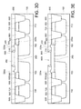
- FIG. 1 shows a schematic cross-sectional view of a semiconductor device according to the best embodiment of the present invention.
- FIG. 1A shows a schematic cross-sectional view of a semiconductor device according to another embodiment of the present invention.
- FIG. 2 shows a schematic cross-sectional view of a semiconductor device according to yet another embodiment of the present invention.
- FIGS. 3A-3E illustrate a method for forming a semiconductor device according to one embodiment of the present invention.
- FIGS. 4A-4B schematically illustrate a traditional method for forming a semiconductor device.
- FIG. 1 shows a schematic cross-sectional view of a semiconductor device 10 according to one embodiment of the present invention.
- the semiconductor device 10 comprises a substrate 100 , a buried gate dielectric layer 200 , a source and a drain, both denoted by 300 , and a gate electrode 400 .
- the substrate 100 has a recess 100 r in which the buried gate dielectric layer 200 is disposed.
- the buried gate dielectric layer 200 has a planar upper surface 210 and an edge 220 protruding beyond the planar upper surface 210 along a direction substantially perpendicular to the substrate 100 .
- the source 300 and drain 300 are disposed at opposite sides 200 s of the gate dielectric layer 200 .
- the gate electrode 400 is disposed above the gate dielectric layer 200 .
- the gate electrode 400 and the edge 220 of the gate dielectric layer 200 do not overlap along a direction substantially parallel to the substrate 100 .
- the semiconductor device 10 is a high-voltage metal oxide semiconductor device particularly a double-diffused drain (DDD) transistor.
- the thickness of the buried gate dielectric layer 200 is about 1000 ⁇ 100 Angstroms. Elements such as gate electrode, buried gate dielectric layer, source, drain, and the like of the semiconductor device 10 may be larger or smaller in size depending on the operational voltage and/or the breakdown voltage of the device. Therefore, the thickness of the buried gate dielectric layer 200 may range from hundreds of Angstroms to thousands of Angstroms.
- an upper surface 220 a of the edge 220 is higher than the planar upper surface 210 by a step height H 1 ranging from 500 to 600 Angstroms.
- the width W 1 of the edge 220 of the buried gate dielectric layer 200 ranges from 0.12 to 0.15 microns.
- the semiconductor device 10 further comprises a shallow trench isolation structure 600 .
- the shallow trench isolation structure 600 for example surrounds the gate electrode 400 and the source 300 and drain 300 in order to electrically insulate the semiconductor device 10 from other devices.
- the source 300 and drain 300 may respectively extend from opposite sidewalls 200 s of the buried gate dielectric layer 200 to the shallow trench isolation structure 600 .
- there are many processes such as film deposition processes and thermal annealing processes performed during the formation of the semiconductor device 10 , and some of these processes may diffuse dopants in the source 300 and drain 300 , thereby enlarging regions of the source 300 and drain 300 .
- the enlarged source and drain do not overlap with the gate electrode 400 along a direction substantially parallel to the substrate 100 .
- a sidewall 400 s of the gate electrode 400 is spaced a substantial distance D 1 from a sidewall 200 s of the buried gate dielectric layer 200 .
- the substantial distance D 1 may range from 1 to 3 microns. That is, the opposite sidewalls 400 s of the gate electrode 400 are respectively spaced a substantial distance D 1 from the source 300 and the drain 300 .
- outer portions of the buried gate dielectric layer 200 not covered by the gate electrode 400 experience more wet cleaning than that of the center portion of the buried gate dielectric layer 200 covered by the gate electrode 400 , causing the outer portions of the buried gate dielectric layer 200 not covered by the gate electrode 400 to experience more material loss.
- the surface height decreasing caused by material loss ranges from several tens of Angstroms to 100 Angstroms.
- planar upper surface 210 and the edge 220 of the buried gate dielectric layer 200 not covered by the gate electrode 400 suffer more material loss while an upper surface 230 of the center portion of the buried gate dielectric layer covered by the gate electrode (interface between the buried gate dielectric layer 200 and the gate electrode 400 ) suffers less material loss.
- an upper surface 200 a of the edge 220 of the buried gate dielectric layer 200 is generally higher than the upper surface 230 of the buried gate dielectric layer 200 covered by the gate electrode 400 and the upper surface 200 a and the upper surface 230 are both higher than the planar upper surface 210 of the buried gate dielectric layer 200 not covered by the gate electrode 400 .
- whether element 300 is a drain or a source depends on the bias of the external voltage. That on which the external voltage is applied being the source, while the other with the current flowing out therefrom being the drain.
- the gate electrode 400 and the drain 300 are spaced apart by a substantial distance D 1 . In the case where the substantial distance between the gate electrode 400 and the drain 300 is increased, the electric field generated between the gate electrode 400 and the drain 300 is decreased. Because of the weaker electric field, not only will the gate-induced drain leakage (GIDL) be decreased, and further the breakdown voltage of the semiconductor device 10 can be higher.
- the source 300 and drain 300 may be symmetrically disposed with respect to the gate electrode 400 as shown in FIG. 1 . That is, the distance between the gate electrode 400 and the source is substantially equivalent to the distance between the gate electrode 400 and the drain.
- the source 300 and drain 300 may be asymmetrically disposed with respect to the gate electrode 400 as shown in FIG. 1A . That is, the distance D 1 - 1 between one of the source 300 and drain 300 and the gate electrode 400 is substantially smaller than the distance D 1 - 2 between one of the source 300 and drain 300 and the gate electrode 400 .
- a silicide block (SAB) layer for blocking silicide formation is formed on a substrate between the gate electrode and the drain.
- This SAB layer is not only used to define regions to be silicided but also used as an implant mask to define drain region that is spaced a substantial distance from the gate electrode.
- a photomask for SAB layer usually has less accuracy compared to a photomask for a critical layer such as gate electrode, therefore there are lots of limitations imposed by design rule for SAB layer. For example, various substantial distances need to be maintained between the SAB layer and device elements adjacent to the SAB layer.
- the minimum dimension of the SAB layer is 0.2 micron and the minimum distance to be maintained between the SAB layer and a drain contact is 0.18 micron.
- the semiconductor device 10 comprises a buried gate dielectric layer 200 horizontally protruding beyond the gate electrode 400 to form edges 220 so as to separate the gate electrode 400 from the drain 300 by a substantial distance D 1 , thereby improving GIDL effect without using a SAB layer.
- the sidewalls 200 s of the buried gate dielectric layer 200 may also be used as an implant mask for defining source and drain regions, so a self-aligned implant process may be performed to accurately form the source and the drain.
- the semiconductor device of the present invention may be more compact in size.
- the gate electrode 400 does not overlap with the edge 220 of the buried gate dielectric layer 200 along a direction substantially parallel to the substrate 100 and the upper surface 230 of the gate electrode 400 is substantially coplanar with the substrate surface, the planarity of the gate electrode 400 and the overall planarity of the semiconductor device 10 and other devices are not adversely affected, thereby enhancing process integration of the semiconductor device 10 and other devices such as a low voltage transistor.
- the term “low voltage” may refer to an operational voltage equivalent to or less than 5 V.
- the semiconductor 10 may further comprise a lightly doped source region 700 and a lightly doped drain region 700 formed in the substrate 100 .
- the source 300 and the drain 300 are disposed in the lightly doped source region 700 and the lightly doped drain region 700 respectively.
- a portion of the buried gate dielectric layer 200 is disposed above the lightly doped source region 700 and the lightly doped drain region 700 .
- the semiconductor device 10 may further comprise a heavily doped region 720 for a well pickup and a lightly doped region 710 surrounding the heavily doped region 720 .
- the heavily doped region 720 is a P-type heavily doped region
- the lightly doped region 710 is a P-type lightly doped region
- the substrate 100 is a P-type well receiving the doped regions stated above.
- the substrate 100 may further comprises a silicide layer 500 disposed on the source 300 and the drain 300 to form ohmic contact between the source 300 and the drain 300 and later-formed interconnect structures such as contact plugs.
- the silicide layer 500 may also be formed on the heavily doped region 720 .
- the semiconductor device 10 may further comprise at least a spacer 800 disposed on sidewalls 400 s of the gate electrode 400 .
- the spacer 800 may have a single-layered structure of multi-layered structure.
- the thickness of the spacer 800 is several hundred angstroms for example 250-300 angstroms.
- FIG. 2 shows a schematic cross-sectional view of a semiconductor device according to another embodiment of the present invention.
- the elements of this embodiment similar to the elements of the previous embodiment are represented by similar or the same numerical and are not explained in detail.
- the gate electrode 400 of this embodiment may comprise a U-shaped optional barrier layer 410 , a U-shaped work function metal layer 420 , and a low resistivity filling metal 430 .
- the U-shaped optional barrier layer 410 and the U-shaped work function metal layer 420 are conformally disposed in a gate trench (not shown in FIG. but will be explained in connection with the formation of the semiconductor device 20 ), and the low resistivity filling metal 430 is disposed above the work function metal layer 420 .
- a material for the U-shaped work function metal layer 420 may be chosen according to the conductive type such as N type or P type of the semiconductor device 20 .
- an optional barrier may be inserted between the U-shaped work function metal layer 420 and the low resistivity filling metal 430 .
- the semiconductor device 20 may further comprise an interlayer dielectric layer 930 .
- the gate electrode 400 is disposed in the interlayer dielectric layer 930 and an upper surface of the gate electrode 400 is substantially coplanar with an upper surface of the interlayer dielectric layer 930 .
- a material for P type work function metal layer may be titanium nitride (TiN), tantalum nitride (TaN), titanium carbide (TiC), tantalum carbide (TaC), tungsten carbide (WC), or a random combination thereof.
- a material for N type work function metal layer may be titanium aluminum (TiAl), zirconium aluminum (ZrAl), titanium aluminum nitride (TiAlN), tungsten aluminum (WAl), tantalum aluminum (TaAl), hafnium aluminum (HfAl), or a random combination thereof.
- a material for the low resistivity filling metal 430 may be tungsten (W), aluminum (Al), copper (Copper), tantalum aluminum (TaAl), titanium aluminum oxide (TiAlO), or a random combination thereof.
- a material for barrier metal layer may be a metal nitride such as titanium nitride (TiN), tantalum nitride (TaN), or a combination thereof.
- the semiconductor device 10 of embodiment one of the present invention is compared with two traditional semiconductor devices in view of their electrical performances. Such comparison is for illustrating the advantages of the present invention and should not be used to limit the present invention.
- the example 1 uses a doubled diffused drain (DDD) high voltage device having a thick spacer to space gate electrode and drain apart while the example 2 uses a doubled diffused drain (DDD) high voltage device having a silicide blocking (SAB) layer to space gate electrode and drain apart.
- DDD doubled diffused drain
- SAB silicide blocking
- VT threshold voltage
- Id sat drain current
- I OFF leakage current (also called off current)
- I sub represents bulk current
- BVD represents breakdown voltage.
- example 1 From table 1, one would know that the high leakage current (204.461 pA/ ⁇ m) and low breakdown voltage (16.7 V) of example 1 is evidently caused by strong GIDL effect due to a short distance (several hundred angstroms) between the gate electrode and the drain.
- example 2 and the embodiment one of the present invention show very low leakage currents (less than 1 pA/ ⁇ m) and high breakdown voltages (higher than 33 V) due to a long distance (more than 1 microns) between the gate electrode and the drain.
- the semiconductor device 10 of the embodiment one of the present invention is advantageously smaller than the device used in example 2 in size.
- FIGS. 3A-3E illustrate a method for forming a semiconductor device according to one embodiment of the present invention.
- FIGS. 4A-4B schematically illustrate a traditional method for forming a semiconductor device.
- the elements of this embodiment similar to the elements of the previous embodiments are denoted by similar or the same numerical and are not explained in detail.
- a substrate 100 is provided.
- the substrate 100 for example is a single crystal silicon substrate, a silicon-on-insulator (SOI) substrate, or any material substrates suitable for integrated circuit manufacturing. Then, one or more implantation processes are performed to form a P-type well in the substrate 100 .
- SOI silicon-on-insulator
- one or more shallow trench isolation structure 600 are formed to surround a gate electrode to be formed and a source and a drain to be formed.
- the source and drain to be formed may extend from the shallow trench isolation structure 600 to a buried gate dielectric layer to be formed.
- the shallow trench isolation structure 600 is adjacent to the source and drain.
- one or more implantation processes are performed to form a lightly-doped source and lightly-doped drain 700 in the substrate 100 and a lightly-doped region 710 in the substrate 100 .
- the lightly-doped source and lightly-doped drain 700 and the lightly-doped region 710 have opposite conductive types and are separated by the shallow trench isolation structure 600 .
- the source and drain to be formed and a portion of the buried gate dielectric layer to be formed may be formed in the lightly-doped source and lightly-doped drain 700 .
- the lightly-doped source and lightly-doped drain 700 and the lightly-doped region 710 are both formed in the P-type well in the substrate 100 .
- a hard mask layer or a combination of the hard mask layer and an optional underlying cap oxide is blanketly formed on the substrate 100 .
- a material for the hard mask layer 920 may be silicon nitride (SiN), silicon carbide (SiC), silicon oxynitride (SiON), or the like.
- a material for the optional underlying cap oxide may be silicon dioxide (SiO 2 ).
- the hard mask layer and the optional underlying cap oxide layer are patterned by lithography and etching processes, and the substrate 100 is patterned according to the patterned hard mask layer 920 and the patterned optional underlying cap oxide layer 910 by at least one etching process especially anisotropic dry etching process to form a recess 100 r in the substrate 100 .
- the recess 100 r may have a vertical sidewall as shown in FIG. 3B or a tapered sidewall not shown. The sidewall profile of the recess 100 r affects the shape of the buried gate dielectric layer to be formed.
- a buried gate dielectric layer 200 is formed in the recess 100 r , and the patterned hard mask layer 920 and the patterned optional underlying cap oxide layer 910 are removed.
- the buried gate dielectric layer 200 may be formed by thermal oxidizing a surface of the substrate 100 exposed by the recess 100 r not covered by the patterned hard mask layer 920 and the patterned optional underlying cap oxide layer 910 .
- the buried gate dielectric layer 200 may be formed by other ways.
- the buried gate dielectric layer 200 thus formed has a planar upper surface 210 and an edge 220 protruding beyond the planar upper surface 210 along a direction substantially perpendicular to the substrate 100 .
- the buried gate dielectric layer 200 fills in the recess 100 r and has a thickness about 1000 ⁇ 100 angstroms.
- the thickness of the buried gate dielectric layer 200 substantially matches the depth of the recess 100 r . In other words, the buried gate dielectric layer 200 is almost completely buried in the recess 100 r.
- a high voltage device having thicker gate dielectric layer 4201 in a high voltage device region HV and a low voltage device having relatively thin gate dielectric layer 4202 in a logic device region LV are disposed on/in the same substrate 4100 .
- the taller high voltage device due to thicker gate dielectric layer 4201 will suffer more material loss of the dummy gate layer than the dummy gate layer of the shorter low voltage device. As a result, as shown in FIG.
- the dummy gate electrode 4401 thus obtained of the high voltage device will have insufficient thickness to perform its designated functions while the dummy gate electrode 4402 of the low voltage device will have sufficient thickness.
- the buried gate dielectric layer 200 of the present invention is almost completely buried in the substrate 100 particularly in the recess 100 r , therefore it can prevent the high voltage device from becoming taller than the low voltage device, thereby avoiding substantial material loss from the gate electrode of the high voltage device after the chemical mechanical process is performed.
- a gate electrode 400 is formed above the buried gate dielectric layer 200 and does not overlap with edges 220 of the buried gate dielectric layer 200 along a direction substantially parallel to the substrate 100 .
- the gate electrode 400 for example is formed by traditional lithography and etching processes and comprises polysilicon.
- the gate electrode 400 for example is formed by a replacement metal gate method which comprises the steps explained in connection to FIGS. 3D-3E .
- a dummy gate layer and an optional dielectric capping layer are formed above the buried gate dielectric layer 200 .
- the dummy gate layer and the optional dielectric capping layer are patterned by lithography and etching processes to form a dummy gate electrode 450 and an optional dielectric cap (not shown in FIG. 3D ).
- a material for the dummy gate electrode 450 may be polisilicon, amorphous silicon, single crystal silicon, or the like.
- At least one implantation process is performed using the buried gate dielectric layer 200 as an implantation mask to form self-aligned source 300 and drain 300 in the substrate 100 at opposite sides 200 s of the buried gate dielectric layer 200 .
- the source 300 and drain 300 thus formed extend from the shallow trench isolation structure 600 to sidewalls 200 s of the buried gate dielectric layer 200 .
- the buried gate dielectric layer 200 is thick enough, it serves as implantation mask for self-aligned source and drain formation to prevent dopants used in the implantation process from penetrating the buried gate dielectric layer and reaching a region under the dummy gate electrode 450 .
- a sidewall spacer 800 are formed on sidewalls 400 s of the dummy gate electrode 450 .
- the thickness of the sidewall spacer 800 may range from 250 to 300 angstroms.
- the step of forming of the source 300 and drain 300 and the step of forming of the sidewall spacer 800 may be exchanged. That is, the step of forming of the source 300 and drain 300 may be performed after the step of forming of the sidewall spacer 800 is performed.
- a silicide layer 500 is further formed on the source 300 and drain 300 .
- the silicide layer 500 may also be formed on the heavily-doped region 720 .
- one or more dielectric layers are blanketly formed to cover the buried gate dielectric layer, the dummy gate electrode 450 , the silicide layer 600 , the shallow trench isolation structure 600 , and the sidewall spacer 800 .
- a planarization process such as a chemical mechanical polishing process is performed to remove a portion of the dielectric layers so as to expose the dummy gate electrode 450 and to form a polished interlayer dielectric layer 930 with an upper surface substantially flush with an upper surface of the dummy gate electrode 450 .
- the dummy gate electrode 450 may suffer from material loss hence level shift of the upper surface during the chemical mechanical polishing process.
- the dummy gate electrode 450 is removed to form a gate trench 400 t by one or more wet etching processes.
- a barrier layer such as a barrier layer, a work function metal layer, an optional barrier layer, and a low resistivity metal are formed to fill in the gate trench 400 t , and a chemical mechanical polishing process is performed to remove excess materials outside the gate trench 400 t , thereby forming a metallic gate electrode and forming a globally planar surface across the substrate 100 .
- the metallic gate electrode (that is the gate electrode 400 in FIG. 2 ) comprises the optional barrier layer 410 , the work function metal layer 420 , and the low resistivity metal 430 .
- the semiconductor device 20 shown in FIG. 2 is completed.
- the semiconductor devices according to the present invention not only improves GIDL effect and enhances breakdown voltage, but also benefits from self-aligned source and drain implantation processes to have a more compact device size.
Landscapes
- Engineering & Computer Science (AREA)
- Microelectronics & Electronic Packaging (AREA)
- Power Engineering (AREA)
- Physics & Mathematics (AREA)
- Condensed Matter Physics & Semiconductors (AREA)
- General Physics & Mathematics (AREA)
- Computer Hardware Design (AREA)
- Ceramic Engineering (AREA)
- Manufacturing & Machinery (AREA)
- Insulated Gate Type Field-Effect Transistor (AREA)
Abstract
Description
| Idsat | IOFF | Isub | BVD | ||
| VT (V) | (μA/μm) | (pA/μm) | (μA/μm) | (V) | |
| Example 1 | 0.841 | 573.2 | 204.461 | 0.96 | 16.7 |
| Example 2 | 0.837 | 560.3 | 0.169 | 1.35 | 33.1 |
| Embodiment | 0.886 | 555.5 | 0.06 | 1.26 | 33.6 |
| one | |||||
Claims (25)
Priority Applications (2)
| Application Number | Priority Date | Filing Date | Title |
|---|---|---|---|
| US15/235,320 US9741850B1 (en) | 2016-08-12 | 2016-08-12 | Semiconductor device and method for forming the same |
| CN201610679917.8A CN107731920B (en) | 2016-08-12 | 2016-08-17 | Semiconductor device and method for manufacturing the same |
Applications Claiming Priority (1)
| Application Number | Priority Date | Filing Date | Title |
|---|---|---|---|
| US15/235,320 US9741850B1 (en) | 2016-08-12 | 2016-08-12 | Semiconductor device and method for forming the same |
Publications (1)
| Publication Number | Publication Date |
|---|---|
| US9741850B1 true US9741850B1 (en) | 2017-08-22 |
Family
ID=59581292
Family Applications (1)
| Application Number | Title | Priority Date | Filing Date |
|---|---|---|---|
| US15/235,320 Active US9741850B1 (en) | 2016-08-12 | 2016-08-12 | Semiconductor device and method for forming the same |
Country Status (2)
| Country | Link |
|---|---|
| US (1) | US9741850B1 (en) |
| CN (1) | CN107731920B (en) |
Cited By (7)
| Publication number | Priority date | Publication date | Assignee | Title |
|---|---|---|---|---|
| US10224407B2 (en) * | 2017-02-28 | 2019-03-05 | Sandisk Technologies Llc | High voltage field effect transistor with laterally extended gate dielectric and method of making thereof |
| WO2019066895A1 (en) * | 2017-09-29 | 2019-04-04 | Intel Corporation | Doped sti to reduce source/drain diffusion for germanium nmos transistors |
| CN110556425A (en) * | 2018-05-30 | 2019-12-10 | 台湾积体电路制造股份有限公司 | Method for reducing gate-induced drain leakage in semiconductor devices and related apparatus |
| US11114140B1 (en) | 2020-04-23 | 2021-09-07 | HeFeChip Corporation Limited | One time programmable (OTP) bits for physically unclonable functions |
| US11152381B1 (en) * | 2020-04-13 | 2021-10-19 | HeFeChip Corporation Limited | MOS transistor having lower gate-to-source/drain breakdown voltage and one-time programmable memory device using the same |
| US11437082B2 (en) | 2020-05-17 | 2022-09-06 | HeFeChip Corporation Limited | Physically unclonable function circuit having lower gate-to-source/drain breakdown voltage |
| US11488837B2 (en) | 2020-09-23 | 2022-11-01 | United Microelectronics Corp. | Method for fabricating high-voltage (HV) transistor |
Citations (12)
| Publication number | Priority date | Publication date | Assignee | Title |
|---|---|---|---|---|
| US4642666A (en) | 1978-10-13 | 1987-02-10 | International Rectifier Corporation | High power MOSFET with low on-resistance and high breakdown voltage |
| US4907048A (en) | 1987-11-23 | 1990-03-06 | Xerox Corporation | Double implanted LDD transistor self-aligned with gate |
| US5306655A (en) * | 1990-07-24 | 1994-04-26 | Matsushita Electric Industrial Co., Ltd. | Structure and method of manufacture for MOS field effect transistor having lightly doped drain and source diffusion regions |
| US5589411A (en) | 1995-07-28 | 1996-12-31 | United Microelectronics Corporation | Process for fabricating a high-voltage MOSFET |
| US20050275021A1 (en) * | 2003-01-15 | 2005-12-15 | Renesas Technology Corp. | Semiconductor device |
| US7381621B2 (en) | 2003-06-20 | 2008-06-03 | Samsung Electronics Co., Ltd. | Methods of fabricating high voltage MOSFET having doped buried layer |
| US20080166844A1 (en) * | 2001-03-01 | 2008-07-10 | Hynix Semiconductor, Inc. | Method of Forming a Non-volatile Memory Cell Using Off-set Spacers |
| US20090020807A1 (en) * | 2007-07-19 | 2009-01-22 | Dongbu Hitek Co., Ltd. | Semiconductor device and method for fabricating the same |
| US7531438B2 (en) * | 2006-04-20 | 2009-05-12 | Promos Technologies Inc. | Method of fabricating a recess channel transistor |
| US20090321823A1 (en) | 2006-07-19 | 2009-12-31 | Jin Hyo Jung | Semiconductor Device and Manufacturing Method Thereof |
| US20110073965A1 (en) * | 2009-09-28 | 2011-03-31 | Koh Joon-Young | Gate pattern of semiconductor device and method for fabricating the same |
| US20150287797A1 (en) * | 2014-04-04 | 2015-10-08 | United Microelectronics Corp. | High-voltage metal-oxide semiconductor transistor and method of fabricating the same |
Family Cites Families (3)
| Publication number | Priority date | Publication date | Assignee | Title |
|---|---|---|---|---|
| KR100720475B1 (en) * | 2005-07-26 | 2007-05-22 | 동부일렉트로닉스 주식회사 | Transistor and Method of Forming the Same |
| US7585716B2 (en) * | 2007-06-27 | 2009-09-08 | International Business Machines Corporation | High-k/metal gate MOSFET with reduced parasitic capacitance |
| US7863136B2 (en) * | 2008-09-30 | 2011-01-04 | Qimonda Ag | Method of manufacturing integrated circuits including a FET with a gate spacer and a fin |
-
2016
- 2016-08-12 US US15/235,320 patent/US9741850B1/en active Active
- 2016-08-17 CN CN201610679917.8A patent/CN107731920B/en active Active
Patent Citations (13)
| Publication number | Priority date | Publication date | Assignee | Title |
|---|---|---|---|---|
| US4642666B1 (en) | 1978-10-13 | 1998-10-27 | Int Rectifier Corp | High power mosfet with low on-resistance and high breakdown voltage |
| US4642666A (en) | 1978-10-13 | 1987-02-10 | International Rectifier Corporation | High power MOSFET with low on-resistance and high breakdown voltage |
| US4907048A (en) | 1987-11-23 | 1990-03-06 | Xerox Corporation | Double implanted LDD transistor self-aligned with gate |
| US5306655A (en) * | 1990-07-24 | 1994-04-26 | Matsushita Electric Industrial Co., Ltd. | Structure and method of manufacture for MOS field effect transistor having lightly doped drain and source diffusion regions |
| US5589411A (en) | 1995-07-28 | 1996-12-31 | United Microelectronics Corporation | Process for fabricating a high-voltage MOSFET |
| US20080166844A1 (en) * | 2001-03-01 | 2008-07-10 | Hynix Semiconductor, Inc. | Method of Forming a Non-volatile Memory Cell Using Off-set Spacers |
| US20050275021A1 (en) * | 2003-01-15 | 2005-12-15 | Renesas Technology Corp. | Semiconductor device |
| US7381621B2 (en) | 2003-06-20 | 2008-06-03 | Samsung Electronics Co., Ltd. | Methods of fabricating high voltage MOSFET having doped buried layer |
| US7531438B2 (en) * | 2006-04-20 | 2009-05-12 | Promos Technologies Inc. | Method of fabricating a recess channel transistor |
| US20090321823A1 (en) | 2006-07-19 | 2009-12-31 | Jin Hyo Jung | Semiconductor Device and Manufacturing Method Thereof |
| US20090020807A1 (en) * | 2007-07-19 | 2009-01-22 | Dongbu Hitek Co., Ltd. | Semiconductor device and method for fabricating the same |
| US20110073965A1 (en) * | 2009-09-28 | 2011-03-31 | Koh Joon-Young | Gate pattern of semiconductor device and method for fabricating the same |
| US20150287797A1 (en) * | 2014-04-04 | 2015-10-08 | United Microelectronics Corp. | High-voltage metal-oxide semiconductor transistor and method of fabricating the same |
Non-Patent Citations (1)
| Title |
|---|
| Pu et al. "U.S. Appl. No. 15/136,982", filed Apr. 24, 2016, USA. |
Cited By (8)
| Publication number | Priority date | Publication date | Assignee | Title |
|---|---|---|---|---|
| US10224407B2 (en) * | 2017-02-28 | 2019-03-05 | Sandisk Technologies Llc | High voltage field effect transistor with laterally extended gate dielectric and method of making thereof |
| WO2019066895A1 (en) * | 2017-09-29 | 2019-04-04 | Intel Corporation | Doped sti to reduce source/drain diffusion for germanium nmos transistors |
| CN110556425A (en) * | 2018-05-30 | 2019-12-10 | 台湾积体电路制造股份有限公司 | Method for reducing gate-induced drain leakage in semiconductor devices and related apparatus |
| CN110556425B (en) * | 2018-05-30 | 2022-11-29 | 台湾积体电路制造股份有限公司 | Method for reducing gate-induced drain leakage in semiconductor devices and related apparatus |
| US11152381B1 (en) * | 2020-04-13 | 2021-10-19 | HeFeChip Corporation Limited | MOS transistor having lower gate-to-source/drain breakdown voltage and one-time programmable memory device using the same |
| US11114140B1 (en) | 2020-04-23 | 2021-09-07 | HeFeChip Corporation Limited | One time programmable (OTP) bits for physically unclonable functions |
| US11437082B2 (en) | 2020-05-17 | 2022-09-06 | HeFeChip Corporation Limited | Physically unclonable function circuit having lower gate-to-source/drain breakdown voltage |
| US11488837B2 (en) | 2020-09-23 | 2022-11-01 | United Microelectronics Corp. | Method for fabricating high-voltage (HV) transistor |
Also Published As
| Publication number | Publication date |
|---|---|
| CN107731920A (en) | 2018-02-23 |
| CN107731920B (en) | 2020-10-09 |
Similar Documents
| Publication | Publication Date | Title |
|---|---|---|
| US9741850B1 (en) | Semiconductor device and method for forming the same | |
| US10050036B2 (en) | Semiconductor structure having common gate | |
| US7501674B2 (en) | Semiconductor device having fin transistor and planar transistor and associated methods of manufacture | |
| US7071515B2 (en) | Narrow width effect improvement with photoresist plug process and STI corner ion implantation | |
| US8466026B2 (en) | Semiconductor device and method for manufacturing the same | |
| US8183626B2 (en) | High-voltage MOS devices having gates extending into recesses of substrates | |
| US10332882B2 (en) | Semiconductor device having protective structure over shallow trench isolation region and fabricating method thereof | |
| US20160181268A1 (en) | BOUNDARY SCHEME FOR EMBEDDED POLY-SiON CMOS OR NVM IN HKMG CMOS TECHNOLOGY | |
| US8803253B2 (en) | Replacement metal gate process for CMOS integrated circuits | |
| US20080296702A1 (en) | Integrated circuit structures with multiple FinFETs | |
| TWI573274B (en) | Semiconductor structure and manufacturing method thereof | |
| US10205005B1 (en) | Semiconductor device and method for fabricating the same | |
| US10475903B2 (en) | Method of forming transistor with dual spacer | |
| US6469347B1 (en) | Buried-channel semiconductor device, and manufacturing method thereof | |
| US20070120182A1 (en) | Transistor having recess gate structure and method for fabricating the same | |
| US20170365708A1 (en) | Trench power semiconductor device | |
| US20090224327A1 (en) | Plane mos and the method for making the same | |
| US8994122B2 (en) | Semiconductor device having a memory cell region and a peripheral transistor region | |
| US8658491B2 (en) | Manufacturing method of transistor structure having a recessed channel | |
| US20230253496A1 (en) | Semiconductor device and method of fabricating the same | |
| US11437512B2 (en) | Buried channel metal-oxide-semiconductor field-effect transistor (MOSFET) and forming method thereof | |
| KR20180138402A (en) | Semiconductor device and fabricating method of the same | |
| TWI646604B (en) | Semiconductor device and manufacturing method thereof | |
| CN114093766A (en) | Semiconductor device and method for manufacturing the same | |
| US7432168B1 (en) | Method for fabricating semiconductor device with thin gate spacer |
Legal Events
| Date | Code | Title | Description |
|---|---|---|---|
| AS | Assignment |
Owner name: UNITED MICROELECTRONICS CORP., TAIWAN Free format text: ASSIGNMENT OF ASSIGNORS INTEREST;ASSIGNORS:HSIAO, SHIH-YIN;YANG, CHING-CHUNG;CHIANG, PING-HUNG;AND OTHERS;REEL/FRAME:039414/0569 Effective date: 20160809 |
|
| FEPP | Fee payment procedure |
Free format text: PAYOR NUMBER ASSIGNED (ORIGINAL EVENT CODE: ASPN) |
|
| STCF | Information on status: patent grant |
Free format text: PATENTED CASE |
|
| MAFP | Maintenance fee payment |
Free format text: PAYMENT OF MAINTENANCE FEE, 4TH YEAR, LARGE ENTITY (ORIGINAL EVENT CODE: M1551); ENTITY STATUS OF PATENT OWNER: LARGE ENTITY Year of fee payment: 4 |