US9749555B2 - Arithmetic memory with horizontal binning capabilities for imaging systems - Google Patents
Arithmetic memory with horizontal binning capabilities for imaging systems Download PDFInfo
- Publication number
- US9749555B2 US9749555B2 US14/172,741 US201414172741A US9749555B2 US 9749555 B2 US9749555 B2 US 9749555B2 US 201414172741 A US201414172741 A US 201414172741A US 9749555 B2 US9749555 B2 US 9749555B2
- Authority
- US
- United States
- Prior art keywords
- arithmetic
- coupled
- memory circuit
- input
- arithmetic unit
- Prior art date
- Legal status (The legal status is an assumption and is not a legal conclusion. Google has not performed a legal analysis and makes no representation as to the accuracy of the status listed.)
- Active, expires
Links
Images


Classifications
-
- H04N5/347—
-
- H—ELECTRICITY
- H04—ELECTRIC COMMUNICATION TECHNIQUE
- H04N—PICTORIAL COMMUNICATION, e.g. TELEVISION
- H04N25/00—Circuitry of solid-state image sensors [SSIS]; Control thereof
- H04N25/40—Extracting pixel data from image sensors by controlling scanning circuits, e.g. by modifying the number of pixels sampled or to be sampled
- H04N25/46—Extracting pixel data from image sensors by controlling scanning circuits, e.g. by modifying the number of pixels sampled or to be sampled by combining or binning pixels
-
- H—ELECTRICITY
- H04—ELECTRIC COMMUNICATION TECHNIQUE
- H04N—PICTORIAL COMMUNICATION, e.g. TELEVISION
- H04N25/00—Circuitry of solid-state image sensors [SSIS]; Control thereof
- H04N25/70—SSIS architectures; Circuits associated therewith
- H04N25/71—Charge-coupled device [CCD] sensors; Charge-transfer registers specially adapted for CCD sensors
- H04N25/75—Circuitry for providing, modifying or processing image signals from the pixel array
-
- H04N5/378—
Definitions
- This relates generally to imaging systems and, more particularly, to imaging systems that use arithmetic memory to implement horizontal binning.
- Image sensors are commonly used in electronic devices such as cellular telephones, cameras, and computers to capture images.
- an electronic device is provided with an array of image pixels arranged in pixel rows and pixel columns. Circuitry is commonly coupled to each pixel column for reading out image signals from the image pixels.
- each pixel column is connected to a corresponding arithmetic memory block.
- the arithmetic memory block in each column is used to receive signals from the image pixels in that pixel column and can be used to implement correlated double sampling (CDS) and also vertical binning by combining the values of image pixels in different rows.
- CDS correlated double sampling
- the arithmetic memory blocks in this conventional arrangement can only conduct vertical binning but cannot conduct horizontal binning (i.e., the arithmetic memory blocks cannot be used to combine the image pixel values from different columns).
- FIG. 1 is a diagram of an illustrative system that includes an imaging system and a host subsystem in accordance with an embodiment of the present invention.
- FIG. 2 is a diagram of an illustrative image sensor having an array of image pixels and control circuitry coupled to the array of image pixels in accordance with an embodiment of the present invention.
- FIG. 3 is a circuit diagram of a conventional arithmetic memory block.
- FIG. 4 is a table of illustrative horizontal binning schemes that can be implemented using improved arithmetic memory circuitry in accordance with an embodiment of the present invention.
- FIG. 5 is a diagram of illustrative arithmetic memory circuitry configured to implement a 0:1:0 horizontal binning in accordance with an embodiment of the present invention.
- FIG. 6 is a diagram of illustrative arithmetic memory circuitry configured to implement a 0:2:0 horizontal binning in accordance with an embodiment of the present invention.
- FIG. 7 is a diagram of illustrative arithmetic memory circuitry configured to implement a 1:1:1 horizontal binning in accordance with an embodiment of the present invention.
- FIG. 8 is a diagram of illustrative arithmetic memory circuitry configured to implement a 2:2:2 horizontal binning in accordance with an embodiment of the present invention.
- FIG. 9 is a diagram of illustrative arithmetic memory circuitry configured to implement a 1:2:1 horizontal binning in accordance with an embodiment of the present invention.
- FIG. 10 is a diagram of illustrative arithmetic memory circuitry configured to implement a 2:4:2 horizontal binning in accordance with an embodiment of the present invention.
- FIG. 11 is a block diagram of a system employing the embodiments of FIGS. 4-10 in accordance with an embodiment of the present invention.
- a digital camera module may include one or more image sensors that gather incoming light to capture an image.
- imaging systems may form a portion of a larger system such as a surveillance system or a safety system for a vehicle (e.g., an automobile, a bus, or any other vehicle).
- a vehicle safety system images captured by the imaging system may be used by the vehicle safety system to determine environmental conditions surrounding the vehicle.
- vehicle safety systems may include systems such as a parking assistance system, an automatic or semi-automatic cruise control system, an auto-braking system, a collision avoidance system, a lane keeping system (sometimes referred to as a lane drift avoidance system), etc.
- an imaging system may form part of a semi-autonomous or autonomous self-driving vehicle. Such imaging systems may capture images and detect nearby vehicles using those images. If a nearby vehicle is detected in an image, the vehicle safety system may sometimes operate a warning light, a warning alarm, or may activate braking, active steering, or other active collision avoidance measures.
- a vehicle safety system may use continuously captured images from an imaging system having a digital camera module to help avoid collisions with objects (e.g., other automobiles or other environmental objects), to help avoid unintended drifting (e.g., crossing lane markers) or to otherwise assist in the safe operation of a vehicle during any normal operation mode of the vehicle.
- Image sensors may include arrays of image pixels.
- the pixels in the image sensors may include photosensitive elements such as photodiodes that convert the incoming light into electric charge.
- Image sensors may have any number of pixels (e.g., hundreds or thousands or more).
- a typical image sensor may, for example, have hundreds, thousands, or millions of pixels (e.g., megapixels).
- FIG. 1 is a diagram of an illustrative imaging and response system including an imaging system that uses an image sensor to capture images.
- System 100 of FIG. 1 may be an electronic device such as a camera, a cellular telephone, a video camera, a vehicle safety system (e.g., an active braking system or other vehicle safety system), a surveillance system, or other electronic device that captures digital image data
- vehicle safety system e.g., an active braking system or other vehicle safety system
- surveillance system e.g., or other electronic device that captures digital image data
- system 100 may include an imaging system such as imaging system 10 and host subsystems such as host subsystem 20 .
- Imaging system 10 may include camera module 12 .
- Camera module 12 may include one or more image sensors 14 and one or more lenses.
- the lenses in camera module 12 may, as an example, include M*N individual lenses arranged in an M ⁇ N array.
- Individual image sensors 14 may be arranged in a corresponding M ⁇ N image sensor array (as an example).
- the values of M and N may each be equal to or greater than one, may each be equal to or greater than two, may exceed 10, or may have any other suitable values.
- Each image sensor in camera module 12 may be identical or there may be different types of image sensors in a given image sensor array integrated circuit.
- each lens may focus light onto an associated image sensor 14 .
- Image sensor 14 may include photosensitive elements (i.e., pixels) that convert the light into digital data.
- Image sensors may have any number of pixels (e.g., hundreds, thousands, millions, or more).
- a typical image sensor may, for example, have millions of pixels (e.g., megapixels).
- image sensor 14 may include bias circuitry (e.g., source follower load circuits), sample and hold circuitry, correlated double sampling (CDS) circuitry, amplifier circuitry, analog-to-digital (ADC) converter circuitry, data output circuitry, memory (e.g., buffer circuitry), address circuitry, etc.
- bias circuitry e.g., source follower load circuits
- sample and hold circuitry e.g., sample and hold circuitry
- CDS correlated double sampling
- ADC analog-to-digital converter circuitry
- data output circuitry e.g., memory (e.g., buffer circuitry), address circuitry, etc.
- Image processing and data formatting circuitry 16 may be used to perform image processing functions such as data formatting, adjusting white balance and exposure, implementing video image stabilization, face detection, etc. Image processing and data formatting circuitry 16 may also be used to compress raw camera image files if desired (e.g., to Joint Photographic Experts Group or JPEG format).
- JPEG Joint Photographic Experts Group
- camera sensor 14 and image processing and data formatting circuitry 16 are implemented on a common semiconductor substrate (e.g., a common silicon image sensor integrated circuit die).
- a common semiconductor substrate e.g., a common silicon image sensor integrated circuit die.
- camera sensor 14 and image processing circuitry 16 may be formed on separate semiconductor substrates. For example, camera sensor 14 and image processing circuitry 16 may be formed on separate substrates that have been stacked.
- Imaging system 10 may convey acquired image data to host subsystem 20 over path 18 .
- Host subsystem 20 may include an active control system that delivers control signals for controlling vehicle functions such as braking or steering to external devices.
- Host subsystem 20 may include processing software for detecting objects in images, detecting motion of objects between image frames, determining distances to objects in images, filtering or otherwise processing images provided by imaging system 10 .
- Host subsystem 20 may include a warning system configured to disable imaging system 10 and/or generate a warning (e.g., a warning light on an automobile dashboard, an audible warning, or other warning) in the event that verification data associated with an image sensor indicates that the image sensor is not functioning properly.
- a warning e.g., a warning light on an automobile dashboard, an audible warning, or other warning
- system 100 may provide a user with numerous high-level functions. In a computer or advanced cellular telephone, for example, a user may be provided with the ability to run user applications. To implement these functions, host subsystem 20 of system 100 may have input-output devices 22 such as keypads, input-output ports, joysticks, and displays and storage and processing circuitry 24 .
- Storage and processing circuitry 24 may include volatile and nonvolatile memory (e.g., random-access memory, flash memory, hard drives, solid state drives, etc.). Storage and processing circuitry 24 may also include microprocessors, microcontrollers, digital signal processors, application specific integrated circuits, etc.
- camera module 12 includes image sensor 14 and control and processing circuitry 16 .
- Image sensor 14 may include a pixel array such as array 30 of pixels 28 .
- Control circuitry 16 may be coupled to row control circuitry 32 and global data path 44 .
- Row control circuitry 32 may receive row addresses from control circuitry 16 and may supply corresponding row control signals to image pixels 28 over control paths 128 .
- One or more conductive lines such as column lines 40 may be coupled to each column of image pixels 28 in image pixel array 30 .
- Column lines 40 may be used for reading out image signals from image pixels 28 and for supplying bias signals (e.g., bias currents or bias voltages) to image pixels 28 .
- bias signals e.g., bias currents or bias voltages
- Row control circuitry 32 may generate signals on paths 128 as desired. For example, row control circuitry 32 may generate reset signals on reset control lines in paths 128 , transfer signals on transfer control lines in paths 128 , and row select (e.g., row readout) signals on row select control lines in paths 128 to control the operation of array 30 . If desired, row control circuitry 32 and array 30 may be integrated together in a single integrated circuit (as an example).
- Each column line 40 may be coupled to column circuitry such as a column amplifier 42 , an analog-to-digital converter (ADC) circuit 60 , and a column memory circuit 52 .
- ADC circuits 60 may be used to convert analog signals on column lines 40 into corresponding digital signals before outputting to memory circuits 52 .
- Array 30 may have any number of rows and columns. In general, the size of array 30 and the number of rows and columns in array 30 will depend on the particular implementation of image sensor 14 . While rows and columns are generally described herein as being horizontal and vertical, respectively, rows and columns may refer to any grid-like structure (e.g., features described herein as rows may be arranged vertically and features described herein as columns may be arranged horizontally).
- FIG. 3 is a diagram of a conventional column memory circuit 100 sometimes referred to as an arithmetic memory circuit.
- Arithmetic memory circuit 100 includes N arithmetic units 102 connected in a chain (i.e., arithmetic units 102 - 1 , 102 - 2 , . . . , 102 - n connected in series).
- Each arithmetic unit 102 includes a half adder 104 and a flip-flop circuit 106 .
- Half adder 104 in each unit 102 has first and second inputs, a sum output, and a carry output.
- the sum output of half adder 104 is coupled to the data input of the associated flip-flop 106 in the same unit 102 .
- Flip-flop 106 has a data output that is connected to the first input of the half adder in a successive unit 102 .
- the carry output of half adder 104 is connected to the second input of the half adder in a successive unit.
- the second input of half adder 104 in the first arithmetic unit 102 - 1 may receive a bit from a corresponding column ADC circuit.
- the first input of half adder 104 in the first arithmetic unit 102 - 1 may be coupled to a multiplexer 108 .
- Multiplexer 108 has a first (0) input that receives a logic “0” value and a second (1) input that is coupled to the data output of flip-flop 106 in the last arithmetic unit 102 - n via feedback path 110 .
- Flip-flop 106 in each unit 102 is controlled by a clock signal CLK. Connected in this way, the ADC output may be serially fed into arithmetic memory circuit 100 .
- the logic “0” may be fed through multiplexer 108 during loading of the sampled reset signal, whereas the stored reset signal is fed through multiplexer 108 via path 110 during loading of the sampled image signal.
- Units 102 may be configured to subtract the image signal from the reset signal while loading of the sampled image signal to obtain the desired CDS result.
- vertically binning can be implemented using a similar approach by feeding a CDS result from a previous row back to the first unit 102 - 1 during loading of reset/image signals in a newly selected row.
- Arithmetic memory circuitry 100 cannot be implemented to perform horizontal binning. It would therefore be desirable to provide improved column memory circuitry capable of performing horizontal binning in additional to vertical binning.
- FIG. 4 shows an X-Bin 3 operation where data signals read out from every three adjacent columns are “binned” together to produce a combined output.
- the data signals read out from each group of three pixel columns may be referred to herein as OUT_LEFT, OUT_CENTER, and OUT_RIGHT.
- Signals OUT_LEFT, OUT_CENTER, and OUT_RIGHT may represent signals generated at the output of respective column ADCs 60 ( FIG. 1 ).
- a 0:1:0 horizontal binning scheme can be implemented by only outputting the pixel signal from the center column while ignoring the pixel signals from the left and right columns.
- a 0:2:0 horizontal binning scheme can be implemented by outputting twice the pixel signal from the center column while ignoring the pixel signals from the left and right columns.
- a 1:1:1 horizontal binning scheme can be implemented by simply combining the pixel values from the left, center, and right columns (e.g., the combined output is equal to the sum of OUT_LEFT, OUT_CENTER, and OUT_RIGHT).
- a 2:2:2 horizontal binning scheme can be implemented by combining double the pixel values from the left, center, and right columns (e.g., the combined output is equal to the sum of 2*OUT_LEFT, 2*OUT_CENTER, and 2*OUT_RIGHT).
- a 1:2:1 horizontal binning scheme can be implemented by combining the pixel values from the left and right columns with double the pixel value from the center column (e.g., the combined output is equal to the sum of OUT_LEFT, 2*OUT_CENTER, and OUT_RIGHT).
- a 2:4:2 horizontal binning scheme can be implemented by combining double the pixel values from the left and right columns with four times the pixel value from the center column (e.g., the combined output is equal to the sum of 2*OUT_LEFT, 4*OUT_CENTER, and 2*OUT_RIGHT).
- the horizontal binning scheme in which weighting factor is the same for all the combined columns may be referred to as “flat” binning, whereas the horizontal binning scheme in which the center column is weighted more than the left and right columns may be referred to as “center-weighted” binning.
- FIG. 5 is a diagram of an illustrative column arithmetic memory circuit 200 that is configured to provide the 0:1:0 horizontal binning capability.
- arithmetic memory circuitry 200 may include N arithmetic units 201 - 1 , 201 - 2 , 201 - 3 , 204 - 4 , 201 - 5 , . . . , and 201 -N.
- the number of arithmetic units within circuitry 200 may depend on the ADC output bit width and any additional bits such as a sign bit for implementing subtraction and overflow bits.
- Each of the N arithmetic units 201 may include an adder and a flip-flop circuit 203 .
- the adder in each arithmetic unit 201 may be controlled by a signal MODE.
- the adder in each arithmetic unit 201 may be configured to perform addition when MODE has a first value and may be configured to perform subtraction when MODE has a second value that is different than the first value.
- Flip-flop 203 in each arithmetic unit 201 may be controlled by a clock signal CLK.
- First arithmetic unit 201 - 1 may include a first four-input adder 202 - 1
- second arithmetic unit 201 - 2 may include a second four-input adder 202 - 2
- Third arithmetic unit 201 - 3 may include a first three-input adder 204 - 1
- fourth arithmetic unit 201 - 4 may include a second three-input adder 204 - 2
- the fifth arithmetic unit 201 - 5 , the sixth arithmetic unit (not shown), and so on to the N-th arithmetic unit 201 -N may include two-input adders 205 - 1 , . . . , 205 -M, respectively.
- the four-input adders 202 - 1 and 202 - 2 may have a first (A) input, a second (B) input, a third (C) input, a fourth (D) input, a sum (S) output on which the sum of A, B, C, and D is provided, a first propagate output p[ 0 ], and a second propagate output p[ 1 ].
- A A+B+C+D
- A-B-C-D will be provided at the output S.
- the three-input adders 204 - 1 and 204 - 2 may have a first (A) input, a second (B) input, a third (D) input, a sum (S) output on which the sum of A, B, and C is provided, and a propagate output p[ 0 ].
- the result of A+B+D will be provided at the output S.
- A-B-D will be provided at the output S.
- Each of the two input adders 205 - 1 . . . 205 -N may have a first (A) input, a second (D) input, a sum (S) output on which the sum of A and D is provided, and a propagate output p[ 0 ].
- A first
- D second
- S sum
- p[ 0 ] Propagate signal p[ 0 ] may be computed using conventional carry-out and borrow equations suitable for two-input adders that are well known in the art.
- Arithmetic units 201 may be coupled in series in a chain. In particular, the sum output of each arithmetic unit may be coupled to the A input of the subsequent arithmetic unit via an associated flip-flop 203 . In general, the p[ 0 ] output of each arithmetic unit may be coupled to the D input of the subsequent arithmetic unit. When the D input receives the p[ 0 ] propagate signal, input D serves as a carry-in input. Connected in this way, unit 201 - 1 may serve as the least significant bit (LSB) unit, whereas unit 201 -N may serve as the most significant bit (MSB) unit.
- LSB least significant bit
- MSB most significant bit
- the values output by the LSB+1 unit is double that of the LSB unit; the values output by the LSB+2 unit is four times that of the LSB unit, and so on.
- Circuitry may also include a multiplexer 206 having a first (0) input that receives a logic “0,” a second (1) input that is coupled to the sum output of the MSB arithmetic unit 201 -N via feedback path 207 , and an output that is coupled to input A of arithmetic unit 201 - 1 .
- multiplexer 206 may be configured to route the logic “0” from its first input to its output during reset signal readout operations and may be configured to route the bits from feedback path 206 to its output during image signal readout operations to implement correlated double sampling (CDS).
- each arithmetic unit 201 may be configured to subtract the image signal from the reset signal when receiving both the previously stored reset signal via path 207 and the newly acquired image signal.
- adder 202 - 1 may be configured to receive OUT_CENTER (abbreviated as CENTER) at input B and logic zeroes at inputs C and D
- adder 202 - 2 may be configured to receive logic zeroes at inputs B and C.
- the p[ 1 ] output of adder 202 - 1 may be coupled to input B of 204 - 1 via path 210
- the p[ 1 ] output of adder 202 - 2 may be coupled to input B of adder 204 - 2 via path 212 .
- CENTER OUT_CENTER
- arithmetic memory circuit 200 may be configured to provide the 0:2:0 horizontal binning capability (see, e.g., FIG. 6 ).
- adder 202 - 1 may be configured to receive logic zeroes at inputs B, C, and D
- adder 202 - 2 may be configured to receive signal CENTER at input B and logic “0” at input C.
- the p[ 1 ] output of unit 202 - 1 may be coupled to input B of 204 - 1
- the p[ 1 ] output of unit 202 - 2 may be coupled to input B of adder 204 - 2 .
- arithmetic memory circuit 200 may be configured to provide the 1:1:1 flat horizontal binning capability (see, e.g., FIG. 7 ).
- adder 202 - 1 may receive signals CENTER, OUT_RIGHT (abbreviated as RIGHT), and OUT_LEFT (abbreviated as LEFT) at inputs B, C, and D, respectively, whereas adder 202 - 2 receives signal logic zeroes at inputs B and C.
- the p[ 1 ] output of unit 202 - 1 may be coupled to input B of 204 - 1
- the p[ 1 ] output of unit 202 - 2 may be coupled to input B of unit 204 - 2 .
- CENTER, RIGHT, and LEFT signals are coupled to the LSB unit, signals CENTER, RIGHT, and LEFT all contribute evenly to the final result of arithmetic memory circuit 200 .
- arithmetic memory circuit 200 may be configured to provide the 2:2:2 flat horizontal binning capability (see, e.g., FIG. 8 ).
- adder 202 - 1 may receive signals logic zeroes at inputs B, C, and D
- adder 202 - 2 may receive signals OUT_CENTER, OUT_RIGHT, and OUT_LEFT at inputs B, C, and D, respectively.
- the p[ 1 ] output of unit 202 - 1 may be coupled to input B of 204 - 1
- the p[ 1 ] output of unit 202 - 2 may be coupled to input B of adder 204 - 2 .
- signals OUT_CENTER, OUT_RIGHT, and OUT_LEFT all contribute evenly with a weighting factor of two to the final result of arithmetic memory circuit 200 .
- arithmetic memory circuit 200 may be configured to provide the 1:2:1 center-weighted horizontal binning capability (see, e.g., FIG. 9 ).
- adder 202 - 1 may receive signals logic zero at input B and signals OUT_RIGHT and OUT_LEFT at inputs C and D, respectively, whereas adder 202 - 2 may receive signals OUT_CENTER at input B and logic “0” at input C.
- the p[ 1 ] output of unit 202 - 1 may be coupled to input B of 204 - 1
- the p[ 1 ] output of unit 202 - 2 may be coupled to input B of adder 204 - 2 .
- signal OUT_CENTER contributes double the amount relative to signals OUT_RIGHT and OUT_LEFT in the final result of arithmetic memory circuit 200 .
- arithmetic memory circuit 200 may be configured to provide the 2:4:2 center-weighted horizontal binning capability (see, e.g., FIG. 10 ).
- adder 202 - 1 may receive signals logic zeroes at inputs B, C, and D;
- adder 202 - 2 may receive a logic zero at input B, signal OUT_RIGHT at input C, and signal OUT_LEFT at input D;
- adder 204 - 1 may receive signal OUT_CENTER at input B.
- the p[ 1 ] output of adder 202 - 2 may be coupled to input B of unit 204 - 2 via path 212 . Connected in this way, the weighting of signals OUT_RIGHT and OUT_LEFT is doubled while the weighting of signal OUT_CENTER is quadrupled in the final binned output.
- the horizontal binning schemes described above in connection with FIGS. 4-10 are merely illustrative and do not serve to limit the scope of the present invention.
- the routing between units 201 may be dynamically implemented to support the desired horizontal binning configuration (e.g., memory circuit is operable to provide multiple different horizontal binning schemes in different modes).
- other types of horizontal binning schemes such as 1:1:2, 2:1:2, 1:2:2, 1:4:2, 1:1:4, 1:4:4, 0:8:0, 2:8:2, 4:8:4, etc. can be implemented using a similar approach.
- Xbin 2 e.g., horizontal binning in which data from two different columns are combined
- XBin 4 e.g., horizontal binning in which data from four different columns are combined
- XBin 5 e.g., horizontal binning in which data from five different columns are combined
- these horizontal binning schemes may be combined with other well known vertical binning schemes (e.g., using multiplexer 206 to route pixel signals acquired from previous rows via the feedback path) to obtain any desired two-dimension binning arrangement across the image pixel array.
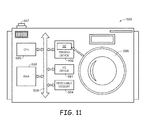
- FIG. 11 shows in simplified form a typical processor system 500 , such as a digital camera, which includes an imaging device 400 .
- Imaging device 400 may include a pixel array 30 having pixels of the type shown in FIG. 2 (e.g., pixel array 30 may be an array of image pixels 28 ) formed on an image sensor SOC.
- Processor system 500 is exemplary of a system having digital circuits that may include imaging device 400 . Without being limiting, such a system may include a computer system, still or video camera system, scanner, machine vision, vehicle navigation, video phone, surveillance system, auto focus system, star tracker system, motion detection system, image stabilization system, and other systems employing an imaging device.
- Processor system 500 may include a lens such as lens 596 for focusing an image onto a pixel array such as pixel array 401 when shutter release button 597 is pressed.
- Processor system 500 may include a central processing unit such as central processing unit (CPU) 595 .
- CPU 595 may be a microprocessor that controls camera functions and one or more image flow functions and communicates with one or more input/output (I/O) devices 591 over a bus such as bus 593 .
- Imaging device 400 may also communicate with CPU 595 over bus 593 .
- System 500 may include random access memory (RAM) 592 and removable memory 594 .
- Removable memory 594 may include flash memory that communicates with CPU 595 over bus 593 .
- Imaging device 400 may be combined with CPU 595 , with or without memory storage, on a single integrated circuit or on a different chip.
- bus 593 is illustrated as a single bus, it may be one or more buses or bridges or other communication paths used to interconnect the system components.
- An imaging system may include one or more image sensors.
- Each image sensor may include an array of image pixels formed on a semiconductor substrate.
- Each image pixel may include one or more photosensitive elements configured to convert incoming light into electric charges.
- Image pixels arranged along a first column in the array may be coupled to a first column line.
- Image pixels arranged along a second column in the array may be coupled to a second column line.
- Image pixels arranged along a third column in the array may be coupled to a third column line.
- the first, second, and third column lines may be coupled to an arithmetic memory circuit and may be considered to be adjacent column lines in the array.
- the arithmetic memory circuit may include a plurality of arithmetic units coupled in series.
- a first arithmetic unit in the chain may serve as an LSB arithmetic unit, whereas the last arithmetic unit in the chain may serve as an MSB arithmetic unit.
- the arithmetic memory circuit may also include a multiplexing circuit having an input that is coupled to the MSB arithmetic unit and an output that is coupled to the first arithmetic unit. Connected as such, the multiplexing circuit can be configured to provide correlated double sampling (CDS) and vertical binning capabilities for the pixel array.
- CDS correlated double sampling
- the arithmetic memory may be operable to provide flat horizontal binning and weighted horizontal binning
- each of the first, second, and third column lines should be coupled to a common arithmetic unit in the arithmetic memory circuit.
- weighted horizontal binning a first portion of the three column lines should be coupled to one of the plurality of arithmetic units, whereas a second portion of the three column lines should be coupled to another one of the plurality of arithmetic units.
- only one of the three adjacent column lines is coupled to a corresponding one of the plurality of arithmetic units in the arithmetic memory circuit.
Abstract
Description
p[1]=A&B&C&D (1)
p[0]=C&(A⊕D)∥B&(A⊕C)∥D&(A⊕B) (2)
where the symbol “&” represents the logic AND function, wherein “⊕” represents the logic XOR function, and where “∥” represents the logic OR function. Computed using
p[1]=!A&B&C&D (3)
p[0]=D&(A˜⊕C)∥!A&(B⊕C)∥B&(C⊕D) (4)
where the symbol “!” represents the logic inversion function and where “˜⊕” represents the logic XNOR function. Computed using
p[0]=(A&B)∥(B&C)∥(C&A) (5)
Computed using equation 5, the propagate signal serves as a “carry out” signal for addition. In the subtract mode, the propagate signals may be computed as follows:
p[0]=(A&B&C)∥(!A&(B∥C)) (6)
Computed using equation 6, the propagate signal serves as a “borrow” signal for subtraction.
Claims (7)
Priority Applications (1)
| Application Number | Priority Date | Filing Date | Title |
|---|---|---|---|
| US14/172,741 US9749555B2 (en) | 2014-02-04 | 2014-02-04 | Arithmetic memory with horizontal binning capabilities for imaging systems |
Applications Claiming Priority (1)
| Application Number | Priority Date | Filing Date | Title |
|---|---|---|---|
| US14/172,741 US9749555B2 (en) | 2014-02-04 | 2014-02-04 | Arithmetic memory with horizontal binning capabilities for imaging systems |
Publications (2)
| Publication Number | Publication Date |
|---|---|
| US20150222825A1 US20150222825A1 (en) | 2015-08-06 |
| US9749555B2 true US9749555B2 (en) | 2017-08-29 |
Family
ID=53755885
Family Applications (1)
| Application Number | Title | Priority Date | Filing Date |
|---|---|---|---|
| US14/172,741 Active 2034-07-28 US9749555B2 (en) | 2014-02-04 | 2014-02-04 | Arithmetic memory with horizontal binning capabilities for imaging systems |
Country Status (1)
| Country | Link |
|---|---|
| US (1) | US9749555B2 (en) |
Families Citing this family (1)
| Publication number | Priority date | Publication date | Assignee | Title |
|---|---|---|---|---|
| US9955096B2 (en) | 2016-03-22 | 2018-04-24 | Taiwan Semiconductor Manufacturing Co., Ltd. | System and method for high-speed down-sampled CMOS image sensor readout |
Citations (18)
| Publication number | Priority date | Publication date | Assignee | Title |
|---|---|---|---|---|
| US6166367A (en) * | 1998-03-26 | 2000-12-26 | Photobit Corporation | Programmable analog arithmetic circuit for imaging sensor |
| US20010015927A1 (en) * | 1998-06-17 | 2001-08-23 | Mitsubishi Denki Kabushiki Kaisha | Synchronous semiconductor memory device having improved operational frequency margin at data input/output |
| US20080084341A1 (en) * | 2006-10-10 | 2008-04-10 | Christian Boemler | Method, apparatus and system providing imager vertical binning and scaling using column parallel sigma-delta digital conversion |
| US20080170137A1 (en) * | 2007-01-17 | 2008-07-17 | Sony Corporation | Solid-state imaging device and imaging apparatus |
| US20080260291A1 (en) * | 2007-04-17 | 2008-10-23 | Nokia Corporation | Image downscaling by binning |
| US7479994B2 (en) | 2004-11-23 | 2009-01-20 | Digital Imaging Systems Gmbh | Image sensor having resolution adjustment employing an analog column averaging/row averaging for high intensity light or row binning for low intensity light |
| US7515183B2 (en) | 2004-11-23 | 2009-04-07 | Digital Imaging Systems Gmbh | Column averaging/row binning circuit for image sensor resolution adjustment in lower intensity light environment |
| US7515783B2 (en) | 2003-09-30 | 2009-04-07 | Japan Aviation Electronics Industry Limited | Micro-optic device and method of manufacturing same |
| US20090237534A1 (en) * | 2008-03-18 | 2009-09-24 | Sony Corporation | Analog-to-digital converter, solid-state image pickup device, and camera system |
| US20090256936A1 (en) * | 2008-04-11 | 2009-10-15 | Canon Kabushiki Kaisha | Method of driving solid-state imaging apparatus |
| US20110074968A1 (en) * | 2009-09-25 | 2011-03-31 | Kim Kyung-Min | Multiple data rate counter, data converter including the same, and image sensor including the same |
| US7991245B2 (en) | 2009-05-29 | 2011-08-02 | Putman Matthew C | Increasing image resolution method employing known background and specimen |
| US20120140089A1 (en) * | 2010-12-06 | 2012-06-07 | Samsung Electronics Co., Ltd. | Image sensor and camera system having the same |
| US8330635B2 (en) * | 2007-09-28 | 2012-12-11 | Sony Corporation | A/D conversion circuit, solid-state image sensor, and camera system |
| US20130063295A1 (en) * | 2011-09-12 | 2013-03-14 | Olympus Corporation | A/d conversion circuit and imaging device |
| US20130089175A1 (en) * | 2011-10-11 | 2013-04-11 | Omnivision Technologies, Inc. | Arithmetic counter circuit, configuration and application for high performance cmos image sensors |
| US8626273B2 (en) | 2010-10-26 | 2014-01-07 | Fujifilm Corporation | Electronic endoscope system having processor device, and method for processing endoscopic image |
| US20140340551A1 (en) * | 2013-05-20 | 2014-11-20 | SK Hynix Inc. | Counting device for reducing power consumption in binning mode and method therefor |
-
2014
- 2014-02-04 US US14/172,741 patent/US9749555B2/en active Active
Patent Citations (18)
| Publication number | Priority date | Publication date | Assignee | Title |
|---|---|---|---|---|
| US6166367A (en) * | 1998-03-26 | 2000-12-26 | Photobit Corporation | Programmable analog arithmetic circuit for imaging sensor |
| US20010015927A1 (en) * | 1998-06-17 | 2001-08-23 | Mitsubishi Denki Kabushiki Kaisha | Synchronous semiconductor memory device having improved operational frequency margin at data input/output |
| US7515783B2 (en) | 2003-09-30 | 2009-04-07 | Japan Aviation Electronics Industry Limited | Micro-optic device and method of manufacturing same |
| US7479994B2 (en) | 2004-11-23 | 2009-01-20 | Digital Imaging Systems Gmbh | Image sensor having resolution adjustment employing an analog column averaging/row averaging for high intensity light or row binning for low intensity light |
| US7515183B2 (en) | 2004-11-23 | 2009-04-07 | Digital Imaging Systems Gmbh | Column averaging/row binning circuit for image sensor resolution adjustment in lower intensity light environment |
| US20080084341A1 (en) * | 2006-10-10 | 2008-04-10 | Christian Boemler | Method, apparatus and system providing imager vertical binning and scaling using column parallel sigma-delta digital conversion |
| US20080170137A1 (en) * | 2007-01-17 | 2008-07-17 | Sony Corporation | Solid-state imaging device and imaging apparatus |
| US20080260291A1 (en) * | 2007-04-17 | 2008-10-23 | Nokia Corporation | Image downscaling by binning |
| US8330635B2 (en) * | 2007-09-28 | 2012-12-11 | Sony Corporation | A/D conversion circuit, solid-state image sensor, and camera system |
| US20090237534A1 (en) * | 2008-03-18 | 2009-09-24 | Sony Corporation | Analog-to-digital converter, solid-state image pickup device, and camera system |
| US20090256936A1 (en) * | 2008-04-11 | 2009-10-15 | Canon Kabushiki Kaisha | Method of driving solid-state imaging apparatus |
| US7991245B2 (en) | 2009-05-29 | 2011-08-02 | Putman Matthew C | Increasing image resolution method employing known background and specimen |
| US20110074968A1 (en) * | 2009-09-25 | 2011-03-31 | Kim Kyung-Min | Multiple data rate counter, data converter including the same, and image sensor including the same |
| US8626273B2 (en) | 2010-10-26 | 2014-01-07 | Fujifilm Corporation | Electronic endoscope system having processor device, and method for processing endoscopic image |
| US20120140089A1 (en) * | 2010-12-06 | 2012-06-07 | Samsung Electronics Co., Ltd. | Image sensor and camera system having the same |
| US20130063295A1 (en) * | 2011-09-12 | 2013-03-14 | Olympus Corporation | A/d conversion circuit and imaging device |
| US20130089175A1 (en) * | 2011-10-11 | 2013-04-11 | Omnivision Technologies, Inc. | Arithmetic counter circuit, configuration and application for high performance cmos image sensors |
| US20140340551A1 (en) * | 2013-05-20 | 2014-11-20 | SK Hynix Inc. | Counting device for reducing power consumption in binning mode and method therefor |
Also Published As
| Publication number | Publication date |
|---|---|
| US20150222825A1 (en) | 2015-08-06 |
Similar Documents
| Publication | Publication Date | Title |
|---|---|---|
| KR200493981Y1 (en) | Imaging systems with real-time digital testing capabilities | |
| US8730330B2 (en) | Image sensors with dark pixels for real-time verification of imaging systems | |
| US10122945B2 (en) | Image sensor with flexible interconnect capabilities | |
| US8953047B2 (en) | Imaging systems with signal chain verification circuitry | |
| US9131211B2 (en) | Imaging systems with verification pixels | |
| US9584800B2 (en) | Imaging systems with pixel array verification circuitry | |
| US9843797B2 (en) | Imaging systems having column readout circuitry with test data injection capabilities | |
| US11758296B2 (en) | Photoelectric conversion device, imaging system, moving body, and exposure control device | |
| US11202023B2 (en) | Imaging device and imaging system | |
| US20170024868A1 (en) | High dynamic range imaging pixels with logarithmic response | |
| US20240080588A1 (en) | Photoelectric conversion device and imaging system | |
| US9749555B2 (en) | Arithmetic memory with horizontal binning capabilities for imaging systems | |
| US11317083B2 (en) | Pixel control signal verification in a stacked image sensor | |
| US11838668B2 (en) | Photoelectric conversion device | |
| US20220357198A1 (en) | Photoelectric conversion apparatus, imaging system, and moving object | |
| US20180295306A1 (en) | Image sensors with diagonal readout | |
| JP7341724B2 (en) | Photoelectric conversion device and photoelectric conversion system | |
| CN110611773B (en) | Image sensor and method of operating the same | |
| CN108366213B (en) | Pixel, imaging method thereof and imaging device | |
| CN112311963A (en) | Image sensor and method of operating the same | |
| US20230292024A1 (en) | Photoelectric conversion device and method of driving photoelectric conversion device | |
| CN113315933B (en) | Comparator, AD converter, photoelectric conversion apparatus, imaging system, and movable body | |
| US20230231979A1 (en) | Image signal processor processing image data having non-bayer pattern and image processing device including same | |
| US11778347B2 (en) | Photoelectric conversion device | |
| US20240040279A1 (en) | Photoelectric conversion device and method of driving photoelectric conversion device |
Legal Events
| Date | Code | Title | Description |
|---|---|---|---|
| AS | Assignment |
Owner name: APTINA IMAGING CORPORATION, CAYMAN ISLANDS Free format text: ASSIGNMENT OF ASSIGNORS INTEREST;ASSIGNOR:IWATA, SHUSUKE;REEL/FRAME:032139/0909 Effective date: 20140204 |
|
| AS | Assignment |
Owner name: SEMICONDUCTOR COMPONENTS INDUSTRIES, LLC, ARIZONA Free format text: ASSIGNMENT OF ASSIGNORS INTEREST;ASSIGNOR:APTINA IMAGING CORPORATION;REEL/FRAME:034673/0001 Effective date: 20141217 |
|
| AS | Assignment |
Owner name: DEUTSCHE BANK AG NEW YORK BRANCH, NEW YORK Free format text: SECURITY INTEREST;ASSIGNOR:SEMICONDUCTOR COMPONENTS INDUSTRIES, LLC;REEL/FRAME:038620/0087 Effective date: 20160415 |
|
| AS | Assignment |
Owner name: DEUTSCHE BANK AG NEW YORK BRANCH, AS COLLATERAL AG Free format text: CORRECTIVE ASSIGNMENT TO CORRECT THE INCORRECT PATENT NUMBER 5859768 AND TO RECITE COLLATERAL AGENT ROLE OF RECEIVING PARTY IN THE SECURITY INTEREST PREVIOUSLY RECORDED ON REEL 038620 FRAME 0087. ASSIGNOR(S) HEREBY CONFIRMS THE SECURITY INTEREST;ASSIGNOR:SEMICONDUCTOR COMPONENTS INDUSTRIES, LLC;REEL/FRAME:039853/0001 Effective date: 20160415 Owner name: DEUTSCHE BANK AG NEW YORK BRANCH, AS COLLATERAL AGENT, NEW YORK Free format text: CORRECTIVE ASSIGNMENT TO CORRECT THE INCORRECT PATENT NUMBER 5859768 AND TO RECITE COLLATERAL AGENT ROLE OF RECEIVING PARTY IN THE SECURITY INTEREST PREVIOUSLY RECORDED ON REEL 038620 FRAME 0087. ASSIGNOR(S) HEREBY CONFIRMS THE SECURITY INTEREST;ASSIGNOR:SEMICONDUCTOR COMPONENTS INDUSTRIES, LLC;REEL/FRAME:039853/0001 Effective date: 20160415 |
|
| STCF | Information on status: patent grant |
Free format text: PATENTED CASE |
|
| MAFP | Maintenance fee payment |
Free format text: PAYMENT OF MAINTENANCE FEE, 4TH YEAR, LARGE ENTITY (ORIGINAL EVENT CODE: M1551); ENTITY STATUS OF PATENT OWNER: LARGE ENTITY Year of fee payment: 4 |
|
| AS | Assignment |
Owner name: FAIRCHILD SEMICONDUCTOR CORPORATION, ARIZONA Free format text: RELEASE OF SECURITY INTEREST IN PATENTS RECORDED AT REEL 038620, FRAME 0087;ASSIGNOR:DEUTSCHE BANK AG NEW YORK BRANCH, AS COLLATERAL AGENT;REEL/FRAME:064070/0001 Effective date: 20230622 Owner name: SEMICONDUCTOR COMPONENTS INDUSTRIES, LLC, ARIZONA Free format text: RELEASE OF SECURITY INTEREST IN PATENTS RECORDED AT REEL 038620, FRAME 0087;ASSIGNOR:DEUTSCHE BANK AG NEW YORK BRANCH, AS COLLATERAL AGENT;REEL/FRAME:064070/0001 Effective date: 20230622 |