US9799412B2 - Memory having a plurality of memory cells and a plurality of word lines - Google Patents
Memory having a plurality of memory cells and a plurality of word lines Download PDFInfo
- Publication number
- US9799412B2 US9799412B2 US14/502,077 US201414502077A US9799412B2 US 9799412 B2 US9799412 B2 US 9799412B2 US 201414502077 A US201414502077 A US 201414502077A US 9799412 B2 US9799412 B2 US 9799412B2
- Authority
- US
- United States
- Prior art keywords
- word line
- memory
- word lines
- replacement
- memory cells
- Prior art date
- Legal status (The legal status is an assumption and is not a legal conclusion. Google has not performed a legal analysis and makes no representation as to the accuracy of the status listed.)
- Active
Links
Images


Classifications
-
- G—PHYSICS
- G11—INFORMATION STORAGE
- G11C—STATIC STORES
- G11C13/00—Digital stores characterised by the use of storage elements not covered by groups G11C11/00, G11C23/00, or G11C25/00
- G11C13/0002—Digital stores characterised by the use of storage elements not covered by groups G11C11/00, G11C23/00, or G11C25/00 using resistive RAM [RRAM] elements
- G11C13/0021—Auxiliary circuits
- G11C13/0069—Writing or programming circuits or methods
-
- G—PHYSICS
- G11—INFORMATION STORAGE
- G11C—STATIC STORES
- G11C29/00—Checking stores for correct operation ; Subsequent repair; Testing stores during standby or offline operation
- G11C29/70—Masking faults in memories by using spares or by reconfiguring
-
- G—PHYSICS
- G11—INFORMATION STORAGE
- G11C—STATIC STORES
- G11C29/00—Checking stores for correct operation ; Subsequent repair; Testing stores during standby or offline operation
- G11C29/70—Masking faults in memories by using spares or by reconfiguring
- G11C29/78—Masking faults in memories by using spares or by reconfiguring using programmable devices
- G11C29/80—Masking faults in memories by using spares or by reconfiguring using programmable devices with improved layout
Definitions
- Memories used for storing data typically have an array of memory cells arranged in rows and columns. Word lines extend along the rows and bit lines extend along the columns to connect to the memory cells.
- Some embodiments relate to a memory that includes a plurality of memory cells, a plurality of bit lines connected to the plurality of memory cells, a plurality of word lines connected to the plurality of memory cells, and a plurality of replacement word lines interspersed among the plurality of word lines.
- the memory also includes a word line control circuit configured to apply different voltages to respective word lines of the plurality of word lines based on positions of the respective word lines.
- the word line control circuit is configured to apply the different voltages to the respective word lines during an operation performed on memory cells of the plurality of memory cells.
- the memory cells are connected to the respective word lines.
- the word line control circuit is configured to replace a defective word line of the plurality of word lines with a replacement word line of the plurality of replacement word lines.
- Some embodiments relate to a method of operating a memory that includes a plurality of memory cells, a plurality of bit lines connected to the plurality of memory cells, a plurality of word lines connected to the plurality of memory cells, a plurality of replacement word lines interspersed among the plurality of word lines, and a word line control circuit.
- the method includes applying, by the word line control circuit, different voltages to respective word lines of the plurality of word lines based on positions of the respective word lines during an operation performed on memory cells of the plurality of memory cells.
- the memory cells are connected to the respective word lines.
- the method also includes replacing a defective word line of the plurality of word lines with a replacement word line of the plurality of replacement word lines.
- Some embodiments relate to a memory that includes a plurality of memory cells, a plurality of bit lines connected to the plurality of memory cells, and a plurality of word lines connected to the plurality of memory cells.
- the plurality of word lines includes a first set of word lines, a second set of word lines and a third set of word lines.
- the memory also includes a plurality of replacement word lines including at least one first replacement word line between the first set of word lines and the second set of word lines, and at least one second replacement word line between the second set of word lines and the third set of word lines.
- the memory further includes a word line control circuit configured to apply different voltages to respective word lines of the plurality of word lines based on positions of the respective word lines.
- the word line control circuit is configured to apply the different voltages to the respective word lines during an operation performed on memory cells of the plurality of memory cells.
- the memory cells are connected to the respective word lines.
- the word line control circuit is configured to replace a defective word line of the first set or the second set with a replacement word line of the at least one first replacement word line.
- FIG. 1 shows an example of a memory, according to some embodiments.
- FIG. 3 shows an exemplary I-V curve for a memory cell of a CBRAM, according to some embodiments.
- FIG. 4 shows an example of a memory including a plurality of tiles, according to some embodiments.
- a memory may include a plurality of replacement word lines that are interspersed throughout the memory between the word lines. If a word line is defective and needs to be replaced, in can be replaced with a nearby replacement word line. In some embodiments, the defective word line can be replaced without needing to change an address-based voltage compensation scheme, as will be described.
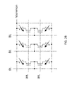
- FIG. 1 shows a diagram of a memory 1 , according to some embodiments.
- Memory 1 includes an array of memory cells me arranged in rows and columns. Each memory cell mc is connected to a word line wl (e.g., wl ⁇ 0>, wl ⁇ 1>, wl ⁇ 2>, wl ⁇ 3>, or wl ⁇ 4>) and a bit line bl (e.g., bl ⁇ 0>, bl ⁇ 1>, bl ⁇ 2>, bl ⁇ 3>, or bl ⁇ 4>).
- the word line control circuit 2 and bit line control circuit 3 address selected memory cell(s) of the array by selecting a corresponding word line and bit line.
- the word lines wl and bit lines bl control writing data into the memory cells me by applying suitable voltages to the word lines wl and bit lines bl.
- the word lines wl and bit lines bl also control reading data from the memory cells me by applying suitable voltages to the word lines wl and reading out the data through the bit lines bl.
- the memory cells me may be any suitable memory cells using any of a variety of technologies, examples of which include resistive random access memory (ReRAM), conductive bridge random access memory (CBRAM), phasechange memory (PCM), magnetoresistive random access memory (MRAM), spin RAM and flash memory, by way of example and not limitation.
- Examples of memory cell configurations include one-transistor (1 T), one-resistor (1R), one-transistor one-resistor (1T1R) and one-drain one-resistor (1D1R), by way of example and not limitation.
- FIG. 2A shows a diagram of an exemplary memory cell mc having a 1T1R configuration, according to some embodiments.
- memory cell mc has a transistor t and a resistive element r.
- the transistor t is an access transistor that controls access to the memory cell mc. Any suitable type of transistor may be used, such as a field effect transistor (FET) or a bipolar transistor, by way of example.
- FET field effect transistor
- Transistor t has a first terminal connected to a bit line bl, a second terminal connected to a first terminal of the resistive element r and a control terminal connected to the word line wl.
- the second terminal of the resistive element r is connected to a common voltage node Vcommon.
- memory cell mc is a three-terminal device connected to the bit line bl, word line wl and common voltage node Vcommon.
- FIG. 2B shows a configuration of a memory, according to some embodiments, in which a common voltage node Vcommon, also termed “plate,” is connected to a plurality of memory cells.
- Vcommon also termed “plate”
- memory cells adjacent to one another within a column of the memory share a connection to the corresponding bit line bl.
- the “reset” operation causes migration of the conductive material in the opposite direction, thereby removing the conductive bridge and increasing the resistance of the memory cell to store a bit of a second polarity.
- FIG. 3 shows an example of applying a current to a CBRAM memory cell, the techniques described herein are not limited to CBRAM. As mentioned above, the techniques described herein may be applied to other types of memory, including other types of nonvolatile memory.
- the bit line voltage at memory cells connected to different word lines of a column may be different depending on the word line address of the memory cell.
- a memory cell with a lower word line address e.g., wl ⁇ 0>
- a memory cell with a higher word line address e.g., wl ⁇ 4>
- a memory cell at a higher word line address will have a higher impedance between the memory cell and the bit line control circuit 3 than a memory cell that has at a lower word line address.
- the voltage applied by the bit line control circuit 3 drops along the length of the bit line, such that a memory cell with a higher word line address sees a lower bit line voltage than that seen by a memory cell with a lower word line address.
- the change in the voltage of the bit line at different word line addresses affects the current that is applied to the memory cells, as shown in FIG. 2A , as the current through the memory cell is proportional to the difference between the bit line voltage and Vcommon.
- the current through a memory cell can be adjusted by the voltage that is applied to the control terminal of transistor t, as doing so changes the resistance of the memory cell.
- the voltage applied to the word line wl can be selected to compensate for the change in the voltage of the bit line at different word line addresses.
- the word line control circuit 2 may apply different voltages to different word lines depending on their word line addresses, such that memory cells connected to different word lines will receive substantially the same current during an operation such as a “set” or “reset” operation.
- Such an address compensation technique may be complex or ineffective if a word line is defective and needs to be replaced with a replacement word line, as the replacement word line may be located at a different position that receives a different bit line voltage due to the change in bit line voltage at different positions.
- the word line control circuit 2 may be designed to compensate for the change in location of the word line when a defective word line is replaced. However, doing so may result in additional complexity for the word line control circuit 2 , which may not be feasible.
- a memory may have a plurality of “tiles.”
- a first word line control circuit 2 may drive word lines for one or more tiles, while another word line control circuit 2 may drive the word lines for other tile(s).
- a tile may include about 1000 word lines wl.
- the techniques described herein are not limited as to a particular number of word lines in a tile.
- the word line control circuit 2 may need to track the tile(s) in which the word line has been replaced, and generate a suitable word line voltage for the replaced word line in the tile(s) in which has been replaced, as well as generate another voltage for the word line in tile(s) where it has not been replaced.
- a compensation technique may not be feasible or may lead to undesirable complexity and/or size of the word line control circuit(s) and/or voltage generators.
- a memory may include a plurality of replacement word lines that are interspersed throughout the memory between the word lines. If a word line is defective and needs to be replaced, in can be replaced with a nearby replacement word line.
- the replacement word lines can be positioned at intervals throughout the array such that a defective word line can be replaced with a replacement word line that is located in a position not significantly different from that of the defective word line. Since the position of the replacement word line is not significantly different from that of the defective word line, the impedance of the bit line to reach the memory cell does not change significantly when the word line is replaced, and the bit line voltage of the replacement word line is not significantly different from that of the word line that has been replaced.
- the current provided to the memory cells connected to the replacement word line during an operation such as a “set” or “reset” operation does not change significantly with respect to the current that would have been provided to the defective word line. Accordingly, in some embodiments the address compensation technique does not need to be changed when a defective word line is replaced with a nearby replacement word line.
- such replacement may be performed by the word line control circuit 2 when the word line control circuit 2 determines that a word line is defective and needs to be replaced.
- defective word line(s) may be replaced as follows. In the event that a word line from wl ⁇ 0> to wl ⁇ n ⁇ 1> is defective, it may be replaced with replacement word line rep_wl_0. In the event that a word line from wl ⁇ n> to wl ⁇ 2n ⁇ 1> is defective, it may be replaced with replacement word line rep_wl_1. In the context of FIG. 5 , a defective word line may be replaced with a replacement word line located above or below the defective word line, as the techniques described herein are not limited in this respect.
- replacement word lines may be interspersed throughout the memory.
- a replacement word line may be positioned at regular intervals (e.g., every n word lines), such that a replacement word line is positioned between successive groups of n word lines. Any suitable value of n may be used, such as 64, 128, or any other suitable value.
- the number of word lines n between replacement word lines may be selected such that a defective word line can be replaced by a replacement word line that is located close enough to the defective word line such that the difference in the voltage of the bit line bl between the defective word line and the replacement word line is below a predetermined threshold.
- a defective word line may be replaced with a replacement word line located above or below the defective word line, as the techniques described herein are not limited in this respect.
- a defective word line from wl ⁇ n> to wl ⁇ 2n ⁇ 1> may be replaced with replacement word line rep_wl_0 or rep_wl_1, located above word lines wl ⁇ n> to wl ⁇ 2n ⁇ 1> in FIG. 6 .
Abstract
Description
Claims (17)
Priority Applications (6)
| Application Number | Priority Date | Filing Date | Title |
|---|---|---|---|
| US14/502,077 US9799412B2 (en) | 2014-09-30 | 2014-09-30 | Memory having a plurality of memory cells and a plurality of word lines |
| TW104127554A TWI716357B (en) | 2014-09-30 | 2015-08-24 | Memory with distributed replacement word lines |
| KR1020177007402A KR102414607B1 (en) | 2014-09-30 | 2015-09-17 | Memory with distributed replacement word lines |
| JP2017516180A JP6772128B2 (en) | 2014-09-30 | 2015-09-17 | Memory with multiple distributed replacement word lines |
| CN201580052543.0A CN107077889B (en) | 2014-09-30 | 2015-09-17 | Memory with distributed replacement word lines |
| PCT/JP2015/004776 WO2016051715A1 (en) | 2014-09-30 | 2015-09-17 | Memory with distributed replacement word lines |
Applications Claiming Priority (1)
| Application Number | Priority Date | Filing Date | Title |
|---|---|---|---|
| US14/502,077 US9799412B2 (en) | 2014-09-30 | 2014-09-30 | Memory having a plurality of memory cells and a plurality of word lines |
Publications (2)
| Publication Number | Publication Date |
|---|---|
| US20160093402A1 US20160093402A1 (en) | 2016-03-31 |
| US9799412B2 true US9799412B2 (en) | 2017-10-24 |
Family
ID=54293302
Family Applications (1)
| Application Number | Title | Priority Date | Filing Date |
|---|---|---|---|
| US14/502,077 Active US9799412B2 (en) | 2014-09-30 | 2014-09-30 | Memory having a plurality of memory cells and a plurality of word lines |
Country Status (6)
| Country | Link |
|---|---|
| US (1) | US9799412B2 (en) |
| JP (1) | JP6772128B2 (en) |
| KR (1) | KR102414607B1 (en) |
| CN (1) | CN107077889B (en) |
| TW (1) | TWI716357B (en) |
| WO (1) | WO2016051715A1 (en) |
Families Citing this family (39)
| Publication number | Priority date | Publication date | Assignee | Title |
|---|---|---|---|---|
| US9324398B2 (en) | 2013-02-04 | 2016-04-26 | Micron Technology, Inc. | Apparatuses and methods for targeted refreshing of memory |
| US9047978B2 (en) | 2013-08-26 | 2015-06-02 | Micron Technology, Inc. | Apparatuses and methods for selective row refreshes |
| JP2015219938A (en) * | 2014-05-21 | 2015-12-07 | マイクロン テクノロジー, インク. | Semiconductor device |
| JP2017182854A (en) | 2016-03-31 | 2017-10-05 | マイクロン テクノロジー, インク. | Semiconductor device |
| US10490251B2 (en) | 2017-01-30 | 2019-11-26 | Micron Technology, Inc. | Apparatuses and methods for distributing row hammer refresh events across a memory device |
| US10580475B2 (en) | 2018-01-22 | 2020-03-03 | Micron Technology, Inc. | Apparatuses and methods for calculating row hammer refresh addresses in a semiconductor device |
| WO2019222960A1 (en) | 2018-05-24 | 2019-11-28 | Micron Technology, Inc. | Apparatuses and methods for pure-time, self adopt sampling for row hammer refresh sampling |
| US10726922B2 (en) | 2018-06-05 | 2020-07-28 | Sandisk Technologies Llc | Memory device with connected word lines for fast programming |
| US11152050B2 (en) | 2018-06-19 | 2021-10-19 | Micron Technology, Inc. | Apparatuses and methods for multiple row hammer refresh address sequences |
| US10685696B2 (en) | 2018-10-31 | 2020-06-16 | Micron Technology, Inc. | Apparatuses and methods for access based refresh timing |
| CN113168861A (en) | 2018-12-03 | 2021-07-23 | 美光科技公司 | Semiconductor device for performing row hammer refresh operation |
| CN117198356A (en) | 2018-12-21 | 2023-12-08 | 美光科技公司 | Apparatus and method for timing interleaving for targeted refresh operations |
| US10770127B2 (en) | 2019-02-06 | 2020-09-08 | Micron Technology, Inc. | Apparatuses and methods for managing row access counts |
| US11043254B2 (en) | 2019-03-19 | 2021-06-22 | Micron Technology, Inc. | Semiconductor device having cam that stores address signals |
| US11227649B2 (en) | 2019-04-04 | 2022-01-18 | Micron Technology, Inc. | Apparatuses and methods for staggered timing of targeted refresh operations |
| US11264096B2 (en) | 2019-05-14 | 2022-03-01 | Micron Technology, Inc. | Apparatuses, systems, and methods for a content addressable memory cell with latch and comparator circuits |
| US11158364B2 (en) | 2019-05-31 | 2021-10-26 | Micron Technology, Inc. | Apparatuses and methods for tracking victim rows |
| US11069393B2 (en) | 2019-06-04 | 2021-07-20 | Micron Technology, Inc. | Apparatuses and methods for controlling steal rates |
| US11158373B2 (en) | 2019-06-11 | 2021-10-26 | Micron Technology, Inc. | Apparatuses, systems, and methods for determining extremum numerical values |
| US10832792B1 (en) | 2019-07-01 | 2020-11-10 | Micron Technology, Inc. | Apparatuses and methods for adjusting victim data |
| US11139015B2 (en) | 2019-07-01 | 2021-10-05 | Micron Technology, Inc. | Apparatuses and methods for monitoring word line accesses |
| US11386946B2 (en) | 2019-07-16 | 2022-07-12 | Micron Technology, Inc. | Apparatuses and methods for tracking row accesses |
| US10943636B1 (en) | 2019-08-20 | 2021-03-09 | Micron Technology, Inc. | Apparatuses and methods for analog row access tracking |
| US10964378B2 (en) | 2019-08-22 | 2021-03-30 | Micron Technology, Inc. | Apparatus and method including analog accumulator for determining row access rate and target row address used for refresh operation |
| US11200942B2 (en) | 2019-08-23 | 2021-12-14 | Micron Technology, Inc. | Apparatuses and methods for lossy row access counting |
| US11302374B2 (en) | 2019-08-23 | 2022-04-12 | Micron Technology, Inc. | Apparatuses and methods for dynamic refresh allocation |
| US11302377B2 (en) | 2019-10-16 | 2022-04-12 | Micron Technology, Inc. | Apparatuses and methods for dynamic targeted refresh steals |
| US11309010B2 (en) | 2020-08-14 | 2022-04-19 | Micron Technology, Inc. | Apparatuses, systems, and methods for memory directed access pause |
| US11380382B2 (en) | 2020-08-19 | 2022-07-05 | Micron Technology, Inc. | Refresh logic circuit layout having aggressor detector circuit sampling circuit and row hammer refresh control circuit |
| US11348631B2 (en) | 2020-08-19 | 2022-05-31 | Micron Technology, Inc. | Apparatuses, systems, and methods for identifying victim rows in a memory device which cannot be simultaneously refreshed |
| US11222682B1 (en) | 2020-08-31 | 2022-01-11 | Micron Technology, Inc. | Apparatuses and methods for providing refresh addresses |
| US11557331B2 (en) | 2020-09-23 | 2023-01-17 | Micron Technology, Inc. | Apparatuses and methods for controlling refresh operations |
| US11222686B1 (en) | 2020-11-12 | 2022-01-11 | Micron Technology, Inc. | Apparatuses and methods for controlling refresh timing |
| US11462291B2 (en) | 2020-11-23 | 2022-10-04 | Micron Technology, Inc. | Apparatuses and methods for tracking word line accesses |
| US11264079B1 (en) | 2020-12-18 | 2022-03-01 | Micron Technology, Inc. | Apparatuses and methods for row hammer based cache lockdown |
| US11482275B2 (en) | 2021-01-20 | 2022-10-25 | Micron Technology, Inc. | Apparatuses and methods for dynamically allocated aggressor detection |
| US11600314B2 (en) | 2021-03-15 | 2023-03-07 | Micron Technology, Inc. | Apparatuses and methods for sketch circuits for refresh binning |
| US11664063B2 (en) | 2021-08-12 | 2023-05-30 | Micron Technology, Inc. | Apparatuses and methods for countering memory attacks |
| US11688451B2 (en) | 2021-11-29 | 2023-06-27 | Micron Technology, Inc. | Apparatuses, systems, and methods for main sketch and slim sketch circuit for row address tracking |
Citations (23)
| Publication number | Priority date | Publication date | Assignee | Title |
|---|---|---|---|---|
| US5519657A (en) | 1993-09-30 | 1996-05-21 | Mitsubishi Denki Kabushiki Kaisha | Semiconductor memory device having a redundant memory array and a testing method thereof |
| US5703817A (en) * | 1995-11-17 | 1997-12-30 | Kabushiki Kaisha Toshiba | Semiconductor memory device |
| US5901081A (en) * | 1997-12-18 | 1999-05-04 | Texas Instruments Incorporated | Circuit and method for preconditioning memory word lines across word line boundaries |
| US6018483A (en) * | 1998-12-10 | 2000-01-25 | Siemens Aktiengesellschaft | Distributed block redundancy for memory devices |
| US6052318A (en) * | 1998-12-22 | 2000-04-18 | Siemens Aktiengesellschaft | Repairable semiconductor memory circuit having parrel redundancy replacement wherein redundancy elements replace failed elements |
| US6590815B2 (en) * | 2000-10-13 | 2003-07-08 | Nec Corporation | Semiconductor memory device and method for its test |
| US6671213B2 (en) * | 2002-01-15 | 2003-12-30 | Renesas Technology Corp. | Thin film magnetic memory device having redundancy repair function |
| US20060109716A1 (en) | 2004-11-22 | 2006-05-25 | Samsung Electronics Co., Ltd. | Nonvolatile memory devices and methods of controlling the wordline voltage of the same |
| US7106643B2 (en) * | 1988-10-07 | 2006-09-12 | Renesas Technology Corp. | Method for manufacturing memory device provided with a defect recovery mechanism featuring a redundancy circuit |
| US7257039B2 (en) * | 2003-10-22 | 2007-08-14 | Stmicroelectronics S.R.L. | Bit line discharge control method and circuit for a semiconductor memory |
| US20080316845A1 (en) | 2007-06-20 | 2008-12-25 | Shih-Hsing Wang | Memory row architecture having memory row redundancy repair function |
| US7889548B2 (en) * | 2003-09-08 | 2011-02-15 | Samsung Electronics Co., Ltd. | Method for reducing a reset current for resetting a portion of a phase change material in a memory cell of a phase change memory device and the phase change memory device |
| US20120081964A1 (en) | 2010-09-30 | 2012-04-05 | Haibo Li | Sensing for nand memory based on word line position |
| US8565004B2 (en) * | 2010-06-29 | 2013-10-22 | Panasonic Corporation | Nonvolatile memory device and method for programming the same |
| US8605520B2 (en) * | 2010-09-22 | 2013-12-10 | Magic Technologies, Inc. | Replaceable, precise-tracking reference lines for memory products |
| US8730744B2 (en) * | 2011-06-27 | 2014-05-20 | Fujitsu Semiconductor Limited | Semiconductor memory with redundant word lines, system, and method of manufacturing semiconductor memory |
| US8730754B2 (en) * | 2011-04-12 | 2014-05-20 | Micron Technology, Inc. | Memory apparatus and system with shared wordline decoder |
| US8817530B2 (en) * | 2011-11-17 | 2014-08-26 | Everspin Technologies, Inc. | Data-masked analog and digital read for resistive memories |
| US8848422B2 (en) * | 2011-04-25 | 2014-09-30 | Panasonic Corporation | Variable resistance nonvolatile memory device and driving method thereof |
| US8897063B2 (en) * | 2012-09-07 | 2014-11-25 | Being Advanced Memory Corporation | Multilevel differential sensing in phase change memory |
| US8913450B2 (en) * | 2012-11-19 | 2014-12-16 | Qualcomm Incorporated | Memory cell array with reserved sector for storing configuration information |
| US9007811B1 (en) * | 2012-10-11 | 2015-04-14 | Everspin Technologies, Inc. | Word line driver circuit |
| US9269432B2 (en) * | 2014-01-09 | 2016-02-23 | Micron Technology, Inc. | Memory systems and memory programming methods |
Family Cites Families (7)
| Publication number | Priority date | Publication date | Assignee | Title |
|---|---|---|---|---|
| US5808945A (en) * | 1996-02-21 | 1998-09-15 | Sony Corporation | Semiconductor memory having redundant memory array |
| US5691946A (en) * | 1996-12-03 | 1997-11-25 | International Business Machines Corporation | Row redundancy block architecture |
| KR100481175B1 (en) * | 2002-08-08 | 2005-04-07 | 삼성전자주식회사 | Semiconductor memory device with shift redundancy circuits |
| JP4227974B2 (en) * | 2005-05-27 | 2009-02-18 | エルピーダメモリ株式会社 | Chip information management method, chip information management system, and chip information management program |
| JP2010146665A (en) * | 2008-12-19 | 2010-07-01 | Toshiba Corp | Resistance change type nonvolatile semiconductor memory |
| US8363443B2 (en) * | 2010-02-01 | 2013-01-29 | Unity Semiconductor Corporation | Circuits and techniques to compensate data signals for variations of parameters affecting memory cells in cross-point arrays |
| US9570164B2 (en) * | 2011-08-24 | 2017-02-14 | Rambus Inc. | System and method for performing memory operations on RRAM cells |
-
2014
- 2014-09-30 US US14/502,077 patent/US9799412B2/en active Active
-
2015
- 2015-08-24 TW TW104127554A patent/TWI716357B/en active
- 2015-09-17 JP JP2017516180A patent/JP6772128B2/en active Active
- 2015-09-17 WO PCT/JP2015/004776 patent/WO2016051715A1/en active Application Filing
- 2015-09-17 CN CN201580052543.0A patent/CN107077889B/en active Active
- 2015-09-17 KR KR1020177007402A patent/KR102414607B1/en active IP Right Grant
Patent Citations (23)
| Publication number | Priority date | Publication date | Assignee | Title |
|---|---|---|---|---|
| US7106643B2 (en) * | 1988-10-07 | 2006-09-12 | Renesas Technology Corp. | Method for manufacturing memory device provided with a defect recovery mechanism featuring a redundancy circuit |
| US5519657A (en) | 1993-09-30 | 1996-05-21 | Mitsubishi Denki Kabushiki Kaisha | Semiconductor memory device having a redundant memory array and a testing method thereof |
| US5703817A (en) * | 1995-11-17 | 1997-12-30 | Kabushiki Kaisha Toshiba | Semiconductor memory device |
| US5901081A (en) * | 1997-12-18 | 1999-05-04 | Texas Instruments Incorporated | Circuit and method for preconditioning memory word lines across word line boundaries |
| US6018483A (en) * | 1998-12-10 | 2000-01-25 | Siemens Aktiengesellschaft | Distributed block redundancy for memory devices |
| US6052318A (en) * | 1998-12-22 | 2000-04-18 | Siemens Aktiengesellschaft | Repairable semiconductor memory circuit having parrel redundancy replacement wherein redundancy elements replace failed elements |
| US6590815B2 (en) * | 2000-10-13 | 2003-07-08 | Nec Corporation | Semiconductor memory device and method for its test |
| US6671213B2 (en) * | 2002-01-15 | 2003-12-30 | Renesas Technology Corp. | Thin film magnetic memory device having redundancy repair function |
| US7889548B2 (en) * | 2003-09-08 | 2011-02-15 | Samsung Electronics Co., Ltd. | Method for reducing a reset current for resetting a portion of a phase change material in a memory cell of a phase change memory device and the phase change memory device |
| US7257039B2 (en) * | 2003-10-22 | 2007-08-14 | Stmicroelectronics S.R.L. | Bit line discharge control method and circuit for a semiconductor memory |
| US20060109716A1 (en) | 2004-11-22 | 2006-05-25 | Samsung Electronics Co., Ltd. | Nonvolatile memory devices and methods of controlling the wordline voltage of the same |
| US20080316845A1 (en) | 2007-06-20 | 2008-12-25 | Shih-Hsing Wang | Memory row architecture having memory row redundancy repair function |
| US8565004B2 (en) * | 2010-06-29 | 2013-10-22 | Panasonic Corporation | Nonvolatile memory device and method for programming the same |
| US8605520B2 (en) * | 2010-09-22 | 2013-12-10 | Magic Technologies, Inc. | Replaceable, precise-tracking reference lines for memory products |
| US20120081964A1 (en) | 2010-09-30 | 2012-04-05 | Haibo Li | Sensing for nand memory based on word line position |
| US8730754B2 (en) * | 2011-04-12 | 2014-05-20 | Micron Technology, Inc. | Memory apparatus and system with shared wordline decoder |
| US8848422B2 (en) * | 2011-04-25 | 2014-09-30 | Panasonic Corporation | Variable resistance nonvolatile memory device and driving method thereof |
| US8730744B2 (en) * | 2011-06-27 | 2014-05-20 | Fujitsu Semiconductor Limited | Semiconductor memory with redundant word lines, system, and method of manufacturing semiconductor memory |
| US8817530B2 (en) * | 2011-11-17 | 2014-08-26 | Everspin Technologies, Inc. | Data-masked analog and digital read for resistive memories |
| US8897063B2 (en) * | 2012-09-07 | 2014-11-25 | Being Advanced Memory Corporation | Multilevel differential sensing in phase change memory |
| US9007811B1 (en) * | 2012-10-11 | 2015-04-14 | Everspin Technologies, Inc. | Word line driver circuit |
| US8913450B2 (en) * | 2012-11-19 | 2014-12-16 | Qualcomm Incorporated | Memory cell array with reserved sector for storing configuration information |
| US9269432B2 (en) * | 2014-01-09 | 2016-02-23 | Micron Technology, Inc. | Memory systems and memory programming methods |
Non-Patent Citations (4)
| Title |
|---|
| Aratani et al., A Novel Resistance Memory with High Scalability and Nanosecond Switching. IEEE Electron Devices Meeting (IEDM) 2007. 783-6. |
| Fackenthal et al., A 16Gb ReRAM with 200MB/s Write and 1GB/s Read in 27nm Technology. 2014 IEEE International Solid-State Circuits Conference / Session 19 / Nonvolatile Memory Solutions / 19.7. Feb. 12, 2014;:338-40. |
| International Search Report for International (PCT) Patent Application No. PCT/JP2015/004776 dated Dec. 18, 2015, 5 pages. |
| Otsuka et al., A 4Mb Conductive-Bridge Resistive Memory with 2.3GB/s Read-Throughput and 216MB/s Program-Throughput. 2011 IEEE International Solid-State Circuits Conference / Session 11 / Non-Volatile Memory Solutions / 11.7. Feb. 22, 2011;:210-11. |
Also Published As
| Publication number | Publication date |
|---|---|
| JP2017535016A (en) | 2017-11-24 |
| WO2016051715A1 (en) | 2016-04-07 |
| TW201614647A (en) | 2016-04-16 |
| KR20170062454A (en) | 2017-06-07 |
| JP6772128B2 (en) | 2020-10-21 |
| US20160093402A1 (en) | 2016-03-31 |
| CN107077889A (en) | 2017-08-18 |
| KR102414607B1 (en) | 2022-06-30 |
| TWI716357B (en) | 2021-01-21 |
| CN107077889B (en) | 2021-03-09 |
Similar Documents
| Publication | Publication Date | Title |
|---|---|---|
| US9799412B2 (en) | Memory having a plurality of memory cells and a plurality of word lines | |
| US11393530B2 (en) | Memory cells, memory cell programming methods, memory cell reading methods, memory cell operating methods, and memory devices | |
| US11024378B2 (en) | Memory systems and memory programming methods | |
| US10783961B2 (en) | Memory cells, memory systems, and memory programming methods | |
| US7911824B2 (en) | Nonvolatile memory apparatus | |
| US10410718B2 (en) | Apparatuses and methods for current limitation in threshold switching memories | |
| US8331177B2 (en) | Resistance semiconductor memory device having a bit line supplied with a compensating current based on a leak current detected during a forming operation | |
| KR20170078596A (en) | Nonvolatile memory device | |
| US8976569B2 (en) | Mitigation of inoperable low resistance elements in programable crossbar arrays | |
| JP5989611B2 (en) | Semiconductor memory device and data control method thereof | |
| KR102471567B1 (en) | Memory device and method for controlling the memory device | |
| US20120243295A1 (en) | Nonvolatile semiconductor memory device and method of control therein | |
| US9368206B1 (en) | Capacitor arrangements using a resistive switching memory cell structure | |
| US9842639B1 (en) | Systems and methods for managing read voltages in a cross-point memory array | |
| KR20130098002A (en) | Program method of vertical resistance memory device |
Legal Events
| Date | Code | Title | Description |
|---|---|---|---|
| AS | Assignment |
Owner name: SONY CORPORATION, JAPAN Free format text: ASSIGNMENT OF ASSIGNORS INTEREST;ASSIGNORS:KITAGAWA, MAKOTO;LUTHRA, YOGESH;SIGNING DATES FROM 20150107 TO 20150112;REEL/FRAME:034894/0487 |
|
| AS | Assignment |
Owner name: SONY SEMICONDUCTOR SOLUTIONS CORPORATION, JAPAN Free format text: CHANGE OF NAME;ASSIGNOR:SONY CORPORATION;REEL/FRAME:039635/0495 Effective date: 20160714 |
|
| AS | Assignment |
Owner name: SONY SEMICONDUCTOR SOLUTIONS CORPORATION, JAPAN Free format text: CORRECTIVE ASSIGNMENT TO CORRECT THE NATURE OF CONVEYANCE PREVIOUSLY RECORDED ON REEL 039635 FRAME 0495. ASSIGNOR(S) HEREBY CONFIRMS THE ASSIGNMENT;ASSIGNOR:SONY CORPORATION;REEL/FRAME:040815/0649 Effective date: 20160714 |
|
| STCF | Information on status: patent grant |
Free format text: PATENTED CASE |
|
| MAFP | Maintenance fee payment |
Free format text: PAYMENT OF MAINTENANCE FEE, 4TH YEAR, LARGE ENTITY (ORIGINAL EVENT CODE: M1551); ENTITY STATUS OF PATENT OWNER: LARGE ENTITY Year of fee payment: 4 |
|
| AS | Assignment |
Owner name: SONY SEMICONDUCTOR SOLUTIONS CORPORATION, JAPAN Free format text: CORRECTIVE ASSIGNMENT TO CORRECT THE REMOVE INCORRECT APPLICATION NUMBER 14/572221 AND REPLACE IT WITH 14/527221 PREVIOUSLY RECORDED AT REEL: 040815 FRAME: 0649. ASSIGNOR(S) HEREBY CONFIRMS THE ASSIGNMENT;ASSIGNOR:SONY CORPORATION;REEL/FRAME:058875/0887 Effective date: 20160714 |