US9800204B2 - Integrated circuit capacitor including dual gate silicon-on-insulator transistor - Google Patents
Integrated circuit capacitor including dual gate silicon-on-insulator transistor Download PDFInfo
- Publication number
- US9800204B2 US9800204B2 US14/219,786 US201414219786A US9800204B2 US 9800204 B2 US9800204 B2 US 9800204B2 US 201414219786 A US201414219786 A US 201414219786A US 9800204 B2 US9800204 B2 US 9800204B2
- Authority
- US
- United States
- Prior art keywords
- gate
- dual gate
- conductivity type
- source
- voltage
- Prior art date
- Legal status (The legal status is an assumption and is not a legal conclusion. Google has not performed a legal analysis and makes no representation as to the accuracy of the status listed.)
- Active, expires
Links
- 230000009977 dual effect Effects 0.000 title claims abstract description 123
- 239000003990 capacitor Substances 0.000 title claims abstract description 84
- 239000012212 insulator Substances 0.000 title claims description 5
- 239000000758 substrate Substances 0.000 claims abstract description 18
- 230000005669 field effect Effects 0.000 claims description 22
- 238000010168 coupling process Methods 0.000 claims description 12
- 238000005859 coupling reaction Methods 0.000 claims description 12
- 230000010355 oscillation Effects 0.000 abstract description 2
- 238000010586 diagram Methods 0.000 description 22
- 238000000034 method Methods 0.000 description 19
- 230000008569 process Effects 0.000 description 9
- 230000007423 decrease Effects 0.000 description 7
- VYPSYNLAJGMNEJ-UHFFFAOYSA-N Silicium dioxide Chemical compound O=[Si]=O VYPSYNLAJGMNEJ-UHFFFAOYSA-N 0.000 description 6
- 239000004065 semiconductor Substances 0.000 description 6
- 239000000463 material Substances 0.000 description 5
- 238000004088 simulation Methods 0.000 description 5
- 238000005229 chemical vapour deposition Methods 0.000 description 4
- 238000004519 manufacturing process Methods 0.000 description 4
- 229910052751 metal Inorganic materials 0.000 description 4
- 239000002184 metal Substances 0.000 description 4
- 230000004044 response Effects 0.000 description 4
- 229910052581 Si3N4 Inorganic materials 0.000 description 3
- XUIMIQQOPSSXEZ-UHFFFAOYSA-N Silicon Chemical compound [Si] XUIMIQQOPSSXEZ-UHFFFAOYSA-N 0.000 description 3
- 238000004140 cleaning Methods 0.000 description 3
- 238000000151 deposition Methods 0.000 description 3
- 238000013461 design Methods 0.000 description 3
- 150000002739 metals Chemical class 0.000 description 3
- 229920002120 photoresistant polymer Polymers 0.000 description 3
- 229910052710 silicon Inorganic materials 0.000 description 3
- 239000010703 silicon Substances 0.000 description 3
- 239000000377 silicon dioxide Substances 0.000 description 3
- HQVNEWCFYHHQES-UHFFFAOYSA-N silicon nitride Chemical compound N12[Si]34N5[Si]62N3[Si]51N64 HQVNEWCFYHHQES-UHFFFAOYSA-N 0.000 description 3
- 239000010409 thin film Substances 0.000 description 3
- 238000000231 atomic layer deposition Methods 0.000 description 2
- 230000015572 biosynthetic process Effects 0.000 description 2
- 230000015556 catabolic process Effects 0.000 description 2
- 238000007796 conventional method Methods 0.000 description 2
- 230000008878 coupling Effects 0.000 description 2
- 238000007772 electroless plating Methods 0.000 description 2
- 238000009713 electroplating Methods 0.000 description 2
- 238000005530 etching Methods 0.000 description 2
- 239000010408 film Substances 0.000 description 2
- 238000007667 floating Methods 0.000 description 2
- 230000006872 improvement Effects 0.000 description 2
- 238000004518 low pressure chemical vapour deposition Methods 0.000 description 2
- 238000000623 plasma-assisted chemical vapour deposition Methods 0.000 description 2
- 238000012545 processing Methods 0.000 description 2
- 235000012239 silicon dioxide Nutrition 0.000 description 2
- 238000010561 standard procedure Methods 0.000 description 2
- 239000000126 substance Substances 0.000 description 2
- 235000012431 wafers Nutrition 0.000 description 2
- MYMOFIZGZYHOMD-UHFFFAOYSA-N Dioxygen Chemical compound O=O MYMOFIZGZYHOMD-UHFFFAOYSA-N 0.000 description 1
- 239000004642 Polyimide Substances 0.000 description 1
- 229910052782 aluminium Inorganic materials 0.000 description 1
- XAGFODPZIPBFFR-UHFFFAOYSA-N aluminium Chemical compound [Al] XAGFODPZIPBFFR-UHFFFAOYSA-N 0.000 description 1
- 230000003321 amplification Effects 0.000 description 1
- 230000008859 change Effects 0.000 description 1
- 229910052681 coesite Inorganic materials 0.000 description 1
- 238000004891 communication Methods 0.000 description 1
- 229910052906 cristobalite Inorganic materials 0.000 description 1
- 238000006731 degradation reaction Methods 0.000 description 1
- 230000001419 dependent effect Effects 0.000 description 1
- 239000003989 dielectric material Substances 0.000 description 1
- 229910001882 dioxygen Inorganic materials 0.000 description 1
- 238000005516 engineering process Methods 0.000 description 1
- 230000001747 exhibiting effect Effects 0.000 description 1
- PCHJSUWPFVWCPO-UHFFFAOYSA-N gold Chemical compound [Au] PCHJSUWPFVWCPO-UHFFFAOYSA-N 0.000 description 1
- 229910052737 gold Inorganic materials 0.000 description 1
- 239000010931 gold Substances 0.000 description 1
- 238000011065 in-situ storage Methods 0.000 description 1
- 238000005259 measurement Methods 0.000 description 1
- 238000004377 microelectronic Methods 0.000 description 1
- 238000012986 modification Methods 0.000 description 1
- 230000004048 modification Effects 0.000 description 1
- 238000001451 molecular beam epitaxy Methods 0.000 description 1
- 238000003199 nucleic acid amplification method Methods 0.000 description 1
- 238000000059 patterning Methods 0.000 description 1
- 238000000206 photolithography Methods 0.000 description 1
- 229910021420 polycrystalline silicon Inorganic materials 0.000 description 1
- 229920001721 polyimide Polymers 0.000 description 1
- 229920005591 polysilicon Polymers 0.000 description 1
- 230000001105 regulatory effect Effects 0.000 description 1
- 238000005549 size reduction Methods 0.000 description 1
- 239000007921 spray Substances 0.000 description 1
- 238000005507 spraying Methods 0.000 description 1
- 239000007858 starting material Substances 0.000 description 1
- 229910052682 stishovite Inorganic materials 0.000 description 1
- 238000006467 substitution reaction Methods 0.000 description 1
- 238000003786 synthesis reaction Methods 0.000 description 1
- 238000007736 thin film deposition technique Methods 0.000 description 1
- 230000007704 transition Effects 0.000 description 1
- 229910052905 tridymite Inorganic materials 0.000 description 1
- WFKWXMTUELFFGS-UHFFFAOYSA-N tungsten Chemical compound [W] WFKWXMTUELFFGS-UHFFFAOYSA-N 0.000 description 1
- 229910052721 tungsten Inorganic materials 0.000 description 1
- 239000010937 tungsten Substances 0.000 description 1
- 238000007740 vapor deposition Methods 0.000 description 1
- 238000005406 washing Methods 0.000 description 1
- 238000003631 wet chemical etching Methods 0.000 description 1
Images


Classifications
-
- H—ELECTRICITY
- H01—ELECTRIC ELEMENTS
- H01L—SEMICONDUCTOR DEVICES NOT COVERED BY CLASS H10
- H01L29/00—Semiconductor devices adapted for rectifying, amplifying, oscillating or switching, or capacitors or resistors with at least one potential-jump barrier or surface barrier, e.g. PN junction depletion layer or carrier concentration layer; Details of semiconductor bodies or of electrodes thereof ; Multistep manufacturing processes therefor
- H01L29/66—Types of semiconductor device ; Multistep manufacturing processes therefor
- H01L29/86—Types of semiconductor device ; Multistep manufacturing processes therefor controllable only by variation of the electric current supplied, or only the electric potential applied, to one or more of the electrodes carrying the current to be rectified, amplified, oscillated or switched
- H01L29/92—Capacitors with potential-jump barrier or surface barrier
- H01L29/94—Metal-insulator-semiconductors, e.g. MOS
-
- H—ELECTRICITY
- H03—ELECTRONIC CIRCUITRY
- H03F—AMPLIFIERS
- H03F1/00—Details of amplifiers with only discharge tubes, only semiconductor devices or only unspecified devices as amplifying elements
- H03F1/02—Modifications of amplifiers to raise the efficiency, e.g. gliding Class A stages, use of an auxiliary oscillation
- H03F1/0205—Modifications of amplifiers to raise the efficiency, e.g. gliding Class A stages, use of an auxiliary oscillation in transistor amplifiers
-
- G—PHYSICS
- G05—CONTROLLING; REGULATING
- G05F—SYSTEMS FOR REGULATING ELECTRIC OR MAGNETIC VARIABLES
- G05F3/00—Non-retroactive systems for regulating electric variables by using an uncontrolled element, or an uncontrolled combination of elements, such element or such combination having self-regulating properties
- G05F3/02—Regulating voltage or current
- G05F3/08—Regulating voltage or current wherein the variable is dc
- G05F3/10—Regulating voltage or current wherein the variable is dc using uncontrolled devices with non-linear characteristics
- G05F3/16—Regulating voltage or current wherein the variable is dc using uncontrolled devices with non-linear characteristics being semiconductor devices
-
- H—ELECTRICITY
- H01—ELECTRIC ELEMENTS
- H01L—SEMICONDUCTOR DEVICES NOT COVERED BY CLASS H10
- H01L21/00—Processes or apparatus adapted for the manufacture or treatment of semiconductor or solid state devices or of parts thereof
- H01L21/70—Manufacture or treatment of devices consisting of a plurality of solid state components formed in or on a common substrate or of parts thereof; Manufacture of integrated circuit devices or of parts thereof
- H01L21/77—Manufacture or treatment of devices consisting of a plurality of solid state components or integrated circuits formed in, or on, a common substrate
- H01L21/78—Manufacture or treatment of devices consisting of a plurality of solid state components or integrated circuits formed in, or on, a common substrate with subsequent division of the substrate into plural individual devices
- H01L21/82—Manufacture or treatment of devices consisting of a plurality of solid state components or integrated circuits formed in, or on, a common substrate with subsequent division of the substrate into plural individual devices to produce devices, e.g. integrated circuits, each consisting of a plurality of components
- H01L21/84—Manufacture or treatment of devices consisting of a plurality of solid state components or integrated circuits formed in, or on, a common substrate with subsequent division of the substrate into plural individual devices to produce devices, e.g. integrated circuits, each consisting of a plurality of components the substrate being other than a semiconductor body, e.g. being an insulating body
-
- H—ELECTRICITY
- H01—ELECTRIC ELEMENTS
- H01L—SEMICONDUCTOR DEVICES NOT COVERED BY CLASS H10
- H01L29/00—Semiconductor devices adapted for rectifying, amplifying, oscillating or switching, or capacitors or resistors with at least one potential-jump barrier or surface barrier, e.g. PN junction depletion layer or carrier concentration layer; Details of semiconductor bodies or of electrodes thereof ; Multistep manufacturing processes therefor
- H01L29/66—Types of semiconductor device ; Multistep manufacturing processes therefor
- H01L29/66007—Multistep manufacturing processes
- H01L29/66075—Multistep manufacturing processes of devices having semiconductor bodies comprising group 14 or group 13/15 materials
- H01L29/66083—Multistep manufacturing processes of devices having semiconductor bodies comprising group 14 or group 13/15 materials the devices being controllable only by variation of the electric current supplied or the electric potential applied, to one or more of the electrodes carrying the current to be rectified, amplified, oscillated or switched, e.g. two-terminal devices
- H01L29/66181—Conductor-insulator-semiconductor capacitors, e.g. trench capacitors
-
- H—ELECTRICITY
- H01—ELECTRIC ELEMENTS
- H01L—SEMICONDUCTOR DEVICES NOT COVERED BY CLASS H10
- H01L29/00—Semiconductor devices adapted for rectifying, amplifying, oscillating or switching, or capacitors or resistors with at least one potential-jump barrier or surface barrier, e.g. PN junction depletion layer or carrier concentration layer; Details of semiconductor bodies or of electrodes thereof ; Multistep manufacturing processes therefor
- H01L29/66—Types of semiconductor device ; Multistep manufacturing processes therefor
- H01L29/68—Types of semiconductor device ; Multistep manufacturing processes therefor controllable by only the electric current supplied, or only the electric potential applied, to an electrode which does not carry the current to be rectified, amplified or switched
- H01L29/76—Unipolar devices, e.g. field effect transistors
- H01L29/772—Field effect transistors
- H01L29/78—Field effect transistors with field effect produced by an insulated gate
- H01L29/7831—Field effect transistors with field effect produced by an insulated gate with multiple gate structure
-
- H—ELECTRICITY
- H01—ELECTRIC ELEMENTS
- H01L—SEMICONDUCTOR DEVICES NOT COVERED BY CLASS H10
- H01L29/00—Semiconductor devices adapted for rectifying, amplifying, oscillating or switching, or capacitors or resistors with at least one potential-jump barrier or surface barrier, e.g. PN junction depletion layer or carrier concentration layer; Details of semiconductor bodies or of electrodes thereof ; Multistep manufacturing processes therefor
- H01L29/66—Types of semiconductor device ; Multistep manufacturing processes therefor
- H01L29/68—Types of semiconductor device ; Multistep manufacturing processes therefor controllable by only the electric current supplied, or only the electric potential applied, to an electrode which does not carry the current to be rectified, amplified or switched
- H01L29/76—Unipolar devices, e.g. field effect transistors
- H01L29/772—Field effect transistors
- H01L29/78—Field effect transistors with field effect produced by an insulated gate
- H01L29/786—Thin film transistors, i.e. transistors with a channel being at least partly a thin film
- H01L29/78603—Thin film transistors, i.e. transistors with a channel being at least partly a thin film characterised by the insulating substrate or support
-
- H—ELECTRICITY
- H01—ELECTRIC ELEMENTS
- H01L—SEMICONDUCTOR DEVICES NOT COVERED BY CLASS H10
- H01L29/00—Semiconductor devices adapted for rectifying, amplifying, oscillating or switching, or capacitors or resistors with at least one potential-jump barrier or surface barrier, e.g. PN junction depletion layer or carrier concentration layer; Details of semiconductor bodies or of electrodes thereof ; Multistep manufacturing processes therefor
- H01L29/66—Types of semiconductor device ; Multistep manufacturing processes therefor
- H01L29/68—Types of semiconductor device ; Multistep manufacturing processes therefor controllable by only the electric current supplied, or only the electric potential applied, to an electrode which does not carry the current to be rectified, amplified or switched
- H01L29/76—Unipolar devices, e.g. field effect transistors
- H01L29/772—Field effect transistors
- H01L29/78—Field effect transistors with field effect produced by an insulated gate
- H01L29/786—Thin film transistors, i.e. transistors with a channel being at least partly a thin film
- H01L29/78645—Thin film transistors, i.e. transistors with a channel being at least partly a thin film with multiple gate
- H01L29/78648—Thin film transistors, i.e. transistors with a channel being at least partly a thin film with multiple gate arranged on opposing sides of the channel
-
- H—ELECTRICITY
- H03—ELECTRONIC CIRCUITRY
- H03F—AMPLIFIERS
- H03F3/00—Amplifiers with only discharge tubes or only semiconductor devices as amplifying elements
- H03F3/189—High frequency amplifiers, e.g. radio frequency amplifiers
- H03F3/19—High frequency amplifiers, e.g. radio frequency amplifiers with semiconductor devices only
- H03F3/193—High frequency amplifiers, e.g. radio frequency amplifiers with semiconductor devices only with field-effect devices
-
- H—ELECTRICITY
- H03—ELECTRONIC CIRCUITRY
- H03K—PULSE TECHNIQUE
- H03K17/00—Electronic switching or gating, i.e. not by contact-making and –breaking
- H03K17/51—Electronic switching or gating, i.e. not by contact-making and –breaking characterised by the components used
- H03K17/56—Electronic switching or gating, i.e. not by contact-making and –breaking characterised by the components used by the use, as active elements, of semiconductor devices
- H03K17/687—Electronic switching or gating, i.e. not by contact-making and –breaking characterised by the components used by the use, as active elements, of semiconductor devices the devices being field-effect transistors
-
- H—ELECTRICITY
- H03—ELECTRONIC CIRCUITRY
- H03L—AUTOMATIC CONTROL, STARTING, SYNCHRONISATION, OR STABILISATION OF GENERATORS OF ELECTRONIC OSCILLATIONS OR PULSES
- H03L7/00—Automatic control of frequency or phase; Synchronisation
- H03L7/06—Automatic control of frequency or phase; Synchronisation using a reference signal applied to a frequency- or phase-locked loop
- H03L7/08—Details of the phase-locked loop
- H03L7/085—Details of the phase-locked loop concerning mainly the frequency- or phase-detection arrangement including the filtering or amplification of its output signal
- H03L7/093—Details of the phase-locked loop concerning mainly the frequency- or phase-detection arrangement including the filtering or amplification of its output signal using special filtering or amplification characteristics in the loop
-
- H—ELECTRICITY
- H03—ELECTRONIC CIRCUITRY
- H03F—AMPLIFIERS
- H03F2200/00—Indexing scheme relating to amplifiers
- H03F2200/451—Indexing scheme relating to amplifiers the amplifier being a radio frequency amplifier
Definitions
- FIG. 8C is a schematic diagram of an FD-SOI dual gate PMOS transistor for use as a capacitor in a circuit having a supply voltage of 3.3 V, as described herein.
- FIG. 11B is a schematic diagram of a dual gate NMOS transistor for use as a capacitor in a circuit having an applied bias voltage.
- photoresist can also be used to pattern a hard mask (e.g., a silicon nitride hard mask), which, in turn, can be used to pattern an underlying film.
- a hard mask e.g., a silicon nitride hard mask
- parts of the dual gate PMOS FD-SOI transistor 164 include the primary gate 102 , the source 104 , the drain 106 , and the BOX 112 .
- the source 104 and drain 106 are doped P-type and the channel 165 is doped N-type.
- Inventive parts of the PMOS FD-SOI transistor 164 include a BOX-influenced channel 165 , an NWELL region 167 used as a secondary gate, and an NWELL contact 166 .
- the function of the secondary gate 132 is carried out by the substrate, which is doped to form the NWELL region 167 , in one embodiment.
- the C-V curve 196 shows a capacitance value of 130 fF at a bias voltage of 3.3V, which is twice the best value measured for the reference voltage generator stage 142 .
- the dual gate PMOS FD-SOI transistor 164 when used as the capacitor C 1 and connected as shown, is expected to operate closer to a constant, stable, capacitance value, i.e., in the flat region of the C-V curve, as opposed to the steep linear region or, worse, the bottom of the C-V curve for most of the values of V BIAS from 0 volts to about 3.0 volts, which fails to provide a significant capacitance value at applied bias voltages in the range of about 2.6-3.3 V.
- C 4 is replaced by a dual gate NMOS FD-SOI transistor 211 in which the primary gate is biased at the voltage V BIAS , the source, and drain are both grounded, and the secondary gate is tied to the supply voltage at 3.3 V.
- the dual gate NMOS FD-SOI transistor 211 is similar to the flip-well dual gate NMOS FD-SOI transistor 210 , except that the substrate is P-doped to form a PWELL instead of the NWELL 167 .
Abstract
Dual gate FD-SOI transistors are used as MOSFET capacitors to replace passive well capacitors in analog microcircuits. Use of the dual gate FD-SOI devices helps to reduce unstable oscillations and improve circuit performance. A thick buried oxide layer within the substrate of an FD-SOI transistor forms a capacitive dielectric that can sustain high operating voltages in the range of 1.2 V-3.3 V, above the transistor threshold voltage. A secondary gate in the FD-SOI transistor is used to create a channel from the back side so that even when the bias voltage on the first gate is small, the effective capacitance remains higher. The capacitance of the buried oxide layer is further utilized as a decoupling capacitor between supply and ground. In one example, a dual gate PMOS FD-SOI transistor is coupled to an operational amplifier and a high voltage output driver to produce a precision-controlled voltage reference generator. In another example, two dual gate PMOS and one dual gate NMOS FD-SOI transistor are coupled to a charge pump, a phase frequency detector, and a current-controlled oscillator to produce a high-performance phase locked loop circuit in which the decoupling capacitor footprint is smaller, in comparison to the conventional usage of passive well capacitance.
Description
Technical Field
The present disclosure generally relates to the use of fully depleted silicon-on-insulator (FD-SOI) transistors as substitutes for passive capacitors, and to applications of such capacitive transistor structures in improving performance of analog microcircuits.
Description of the Related Art
Analog microcircuits and, in particular, integrated analog circuits built on semiconductor substrates, are used widely in medical electronics, aerospace systems, and devices equipped with RF communications capability. Such RF-equipped devices include smart phones, tablet computers, microelectronic sensors, and the like. Specific examples of analog microcircuits include reference voltage generator circuits and phase locked loops. Reference voltage generator circuits are used to produce a constant reference voltage in voltage-regulated devices such as power supplies and analog-to-digital converters. Phase locked loop (PLL) circuits are used to perform phase matching between input and output signals of oscillators. Such circuits can be used, for example, in microprocessors for clock synchronization, and in telecommunications for signal demodulation and frequency synthesis.
Capacitors are frequently used as components in analog microcircuits. Various structures that are present on integrated circuit chips can be made available to circuit designers for use as parallel plate capacitors, or such capacitors can be specially designed. Alternatively, it is possible for metal-oxide-semiconductor field effect transistors (MOSFETs), which are ubiquitous on integrated circuit chips, to be used as capacitors in various microcircuits if the components are connected in a particular manner. In a field effect transistor (FET), a thin gate oxide layer between the gate and the channel can be considered a capacitive dielectric, and the gate and the channel regions can be considered two parallel plates of a capacitor. However, because typical gate oxide layers are only a few nm thick, the gate oxide layer tends to be vulnerable and can break down easily in response to application of a gate voltage that is slightly too large. Furthermore, transistors are active, three-terminal devices whereas capacitors are passive, two-terminal devices that are generally much simpler and less expensive to manufacture. For at least these reasons, it is generally not customary to connect transistors in such a way that they can be used as capacitors.
Dual gate FD-SOI transistors are used as MOSFET capacitors in analog microcircuits to reduce unstable oscillations and to improve circuit performance. A primary gate spaced apart from the channel by a gate dielectric layer controls current in the channel of the device. A secondary gate also controls current in the channel, the secondary gate being spaced apart from the channel by a thicker buried dielectric layer within the substrate of the SOI transistors. The thick buried oxide layer acts as a capacitive dielectric that can sustain high operating voltages in the range of 1.2 V-3.3 V, above the transistor threshold voltage, which is typically about 0.5 V. In one embodiment, the dielectric of the gate and the buried layer are oxides, such as SiO2. Such FD-SOI devices can be substituted for parallel plate capacitor components in integrated circuits, to improve circuit performance and efficiency.
In one exemplary embodiment, a dual gate PMOS FD-SOI transistor is coupled to an operational amplifier and a high voltage output driver to produce a precision-controlled voltage reference generator.
In another exemplary embodiment, two dual gate PMOS transistors and one dual gate NMOS FD-SOI transistor are coupled to a charge pump, a phase frequency detector, and a current-controlled oscillator to produce a high-performance phase locked loop circuit in which the decoupling capacitor footprint is significantly smaller.
In the drawings, identical reference numbers identify similar elements. The sizes and relative positions of elements in the drawings are not necessarily drawn to scale.
In the following description, certain specific details are set forth in order to provide a thorough understanding of various aspects of the disclosed subject matter. However, the disclosed subject matter may be practiced without these specific details. In some instances, well-known structures and methods of semiconductor processing comprising embodiments of the subject matter disclosed herein have not been described in detail to avoid obscuring the descriptions of other aspects of the present disclosure.
Throughout the specification and claims that follow, the word “comprise” and variations thereof, such as “comprises” and “comprising” are to be construed in an open, inclusive sense, that is, as “including, but not limited to.”
Reference throughout the specification to “one embodiment” or “an embodiment” means that a particular feature, structure, or characteristic described in connection with the embodiment is included in at least one embodiment. Thus, the appearance of the phrases “in one embodiment” or “in an embodiment” in various places throughout the specification are not necessarily all referring to the same aspect. Furthermore, the particular features, structures, or characteristics may be combined in any suitable manner in one or more aspects of the present disclosure.
Reference throughout the specification to integrated circuits is generally intended to include integrated circuit components built on semiconducting substrates, whether or not the components are coupled together into a circuit or able to be interconnected. Throughout the specification, the term “layer” is used in its broadest sense to include a thin film, a cap, or the like.
Reference throughout the specification to conventional thin film deposition techniques for depositing silicon nitride, silicon dioxide, metals, or similar materials include such processes as chemical vapor deposition (CVD), low-pressure chemical vapor deposition (LPCVD), metal organic chemical vapor deposition (MOCVD), plasma-enhanced chemical vapor deposition (PECVD), plasma vapor deposition (PVD), atomic layer deposition (ALD), molecular beam epitaxy (MBE), electroplating, electro-less plating, and the like. Specific embodiments are described herein with reference to examples of such processes. However, the present disclosure and the reference to certain deposition techniques should not be limited to those described. For example, in some circumstances, a description that references CVD may alternatively be done using PVD, or a description that specifies electroplating may alternatively be accomplished using electro-less plating. Furthermore, reference to conventional techniques of thin film formation may include growing a film in situ. For example, in some embodiments, controlled growth of an oxide to a desired thickness can be achieved by exposing a silicon surface to oxygen gas or to moisture in a heated chamber.
Reference throughout the specification to conventional photolithography techniques, known in the art of semiconductor fabrication for patterning various thin films, includes a spin-expose-develop process sequence typically followed by an etch process. Alternatively or additionally, photoresist can also be used to pattern a hard mask (e.g., a silicon nitride hard mask), which, in turn, can be used to pattern an underlying film.
Reference throughout the specification to conventional etching techniques known in the art of semiconductor fabrication for selective removal of polysilicon, silicon nitride, silicon dioxide, metals, photoresist, polyimide, or similar materials includes such processes as wet chemical etching, reactive ion (plasma) etching (RIE), washing, wet cleaning, pre-cleaning, spray cleaning, chemical-mechanical planarization (CMP) and the like. Specific embodiments are described herein with reference to examples of such processes. However, the present disclosure and the reference to certain deposition techniques should not be limited to those described. In some instances, two such techniques may be interchangeable. For example, stripping photoresist may entail immersing a sample in a wet chemical bath or, alternatively, spraying wet chemicals directly onto the sample.
Specific embodiments are described herein with reference to analog microcircuits and FD-SOI transistor devices that have been produced; however, the present disclosure and the reference to certain materials, dimensions, and the details and ordering of processing steps are exemplary and should not be limited to those shown.
In the figures, identical reference numbers identify similar features or elements. The sizes and relative positions of the features in the figures are not necessarily drawn to scale.
An FD-SOI transistor 120 is shown in FIG. 1B in cross section. Like the partially depleted SOI transistor 100 shown in FIG. 1A , the FD-SOI transistor 120 also has a BOX layer 112. However, the source and drain regions, 124 and 126 respectively, of the FD-SOI device, are shallower than the corresponding source and drain regions, 104 and 106, respectively, of the partially depleted SOI transistor 100. As a result, doping profiles 127 and 128 are effectively vertical, and the charge characteristics of the channel can be set by the doping concentrations such that a fully charge-depleted region 116 forms between the shallow source and drain regions 124 and 126, bounded below by the BOX layer 112, in response to application of a bias voltage to the gate 102. Because all of the material between the source and drain is charge-depleted, the un-depleted portion 119 shown in FIG. 1A has been eliminated as a possible cause of transistor degradation.
To improve performance of the high voltage output driver stage 144, it is desirable to maximize the value of VREFH, and in turn, to maximize VBIAS. Furthermore, it may be desirable to substitute an MOS transistor for the capacitor C1. The effective capacitance of the MOS transistor varies with applied voltage. It can be useful, when designing such an MOS device, to evaluate the effective capacitance for different applied voltages ΔV by plotting a C-V curve that is determined from simulated or actual measurements of the MOS device. Such a C-V curve is shown in FIG. 4 . As VBIAS increases, the voltage across C1 decreases and the effective value of C1 decreases according to the curve 152. As the effective value of C1 decreases, the stability of negative feedback in reference voltage generator stage 142 degrades and hence leads the reference voltage generator circuit towards instability, varying significantly in response to small changes in the voltage across C1. It is desirable to reduce such bias-dependent behavior of the reference voltage generator stage 142 by shifting the C-V curve 152 to the left, to produce a desired C-V curve 154 that has an extended flat region 155. According to the C-V curve 154, at around 0V, the capacitance value C1 remains substantially constant in response to variations in the voltage across C1.
The present inventor has realized that, while it is not possible to produce the desired C-V curve 154 when C1 is a conventional bulk MOS transistor, it is possible to achieve an improved C-V curve when a dual gate SOI transistor of the type shown in FIG. 2 is used. While this dual gate SOI transistor of FIG. 2 is known as a standalone component, the inventors have realized that using it in a circuit of the type shown in FIG. 5 provides a first level of improved behavior of the C-V curve and circuit operation, as shown in FIG. 8D , explained later.
In addition, the inventors also realized that a significantly improved C-V curve 154 results when C1 is formed using a dual gate PMOS FD-SOI transistor. One such circuit configuration that incorporates a dual gate PMOS FD-SOI transistor as the capacitor C1 is shown in FIG. 5 as the FD-SOI reference voltage based output driver circuit 160 having a modified reference voltage generator stage 162. Comparing FIG. 5 with FIG. 3 , in the modified reference voltage generator stage 162, C1 has been replaced by a dual gate SOI transistor. In one embodiment, the dual gate SOI transistor is a dual gate PMOS FD-SOI transistor 164 indicated by a dotted circle. A primary gate of the dual gate SOI or dual gate PMOS FD-SOI transistor 164 is coupled to the output of the op-amp 148 at the voltage VBIAS. Source and drain terminals of the dual gate SOI or dual gate PMOS FD-SOI transistor 164 are both coupled to the supply voltage VDDE, and the secondary gate 132 of the dual gate SOI or dual gate PMOS FD-SOI transistor 164 is grounded.
A portion of the modified reference voltage generator stage 162 shown in FIG. 5 is further detailed in FIG. 6A , in which the dual gate PMOS FD-SOI transistor 164 is represented in physical cross-section with some schematic lines. One alternative embodiment of the cross-section shown in FIG. 6A more clearly shows the capacitive structure of the dual gate PMOS FD-SOI transistor 164. FIG. 6A can be compared with the cross-section of the conventional dual gate SOI transistor 130 shown in FIG. 2 . In the dual gate SOI transistor 130 of FIG. 2 , the channel 108 can be controlled by either a voltage applied to the primary gate 102, or by a voltage applied to the secondary gate 132. When such a transistor is used as a capacitor, the voltage difference between the primary and secondary gates is applied across both gate dielectrics 110, 134.
Turning now to FIG. 6A , parts of the dual gate PMOS FD-SOI transistor 164 include the primary gate 102, the source 104, the drain 106, and the BOX 112. The source 104 and drain 106 are doped P-type and the channel 165 is doped N-type. Inventive parts of the PMOS FD-SOI transistor 164 include a BOX-influenced channel 165, an NWELL region 167 used as a secondary gate, and an NWELL contact 166. In the embodiment shown in FIG. 6A , the function of the secondary gate 132 is carried out by the substrate, which is doped to form the NWELL region 167, in one embodiment. A voltage can be applied to the NWELL region 167 of the substrate via the front side NWELL contact 166, which is grounded in the embodiment shown. The secondary gate, NWELL region 167, is spaced apart from the channel 165 by a large gate oxide layer, which, in the embodiment shown in FIG. 6A , is the BOX layer 112. An alternative, flip well embodiment shown in FIG. 6B provides a PWELL 168 as the secondary gate.
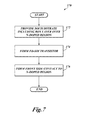
At 172, a starting material is provided as a silicon-on-insulator (SOI) semiconductor wafer that includes the BOX layer 112 deposited over a heavily n-doped region, referred to as the NWELL region 167. The BOX layer 112 has a thickness greater than the front gate so that it can sustain application of up to about ±3.3 V to the NWELL region 167 without experiencing a structural breakdown.
At 174, a field effect transistor is formed by conventional methods used for SOI wafers to provide a top layer of silicon that covers the BOX layer 112. The fully depleted (FD) channel 165 can be achieved by making profiles of the source and drain regions substantially vertical so they are perpendicular to the BOX layer 112.
At 176, the front side NWELL contact 166 can be formed to couple a selected voltage to the secondary gate, which is the NWELL region 167. The front side contact can be made of one or more typical contact metals such as aluminum, tungsten, gold, and the like, or combinations thereof.
A method of operation in which the dual gate PMOS FD-SOI transistor 164 is used as the integrated capacitor C1 entails grounding the NWELL region 167 acting as the secondary gate, coupling both the source and drain regions 104 and 106, respectively, to the supply voltage, VDDE, and applying a voltage VBIAS to the primary gate 102.
Turning now to FIG. 8B , a capacitor option is shown in which C1 is replaced by a dual gate SOI transistor, CPMOS0, as shown in FIG. 2 . The primary gate 102 is biased at the voltage VBIAS and the secondary gate 132, source 104, and drain 106 are all tied to the supply voltage at 3.3 V. Thus, the secondary gate 132 is not used as a fourth terminal separate from the source and drain. This connection provides improved performance, as will be shown.
With reference to FIG. 8C , the capacitance C1 is provided by the dual gate PMOS FD-SOI transistor 164 in which the primary gate 102 is biased at the voltage VBIAS, the source 104, and drain 106 are both tied to the supply voltage at 3.3 V, and the secondary gate 132 is grounded. When the dual gate PMOS FD-SOI transistor 164 is substituted for the capacitor C1, it provides significantly improved performance for use in the circuit of FIG. 5 .
The C-V curve 192 corresponds to the PWELL capacitor C1 of FIG. 8A . The capacitance value starts out high, at about 200 fF when VBIAS is under 1.5 volts, but declines gradually to about 100 fF at VBIAS of 3.0 volts and to only 65 fF when VBIAS is 3.3 volts.
The C-V curve 194 corresponds to a dual gate transistor CPMOS0, such as the one shown in FIG. 2 , exhibiting a more abrupt change, however, the transition occurs at a low voltage. In contrast to the C-V curve 192, the capacitance value drops rapidly for curve 194 associated with the conventional dual gate PMOS transistor CPMOS0, starting to decline at about 2.5 volts and falling in a near vertical line to reach a low capacitance, below 40 fF when VBIAS is about 2.9 volts. As VBIAS reaches its maximum voltage of 3.3 volts, the conventional dual gate PMOS transistor CPMOS0 has a value of only about 35 fF as noted when the line 194 crosses the dotted line 198 at 3.3 volts.
The C-V curve 196 corresponds to the dual gate FDSOI transistor 164 described herein, CPMOS1. Over the entire range of VBIAS, the transistor 164 performs better than the standard capacitor or the conventional dual gate transistor, because the capacitance remains constant up to the highest value of VBIAS, and the capacitance value at 3.3 V is the highest. The improved device performance indicated by the simulation curve 196 predicts a commensurate improvement in circuit performance if the dual gate FDSOI transistor 164 is substituted for the capacitor C1 in the circuit of FIG. 5 . In particular, the C-V curve 196 shows a capacitance value of 130 fF at a bias voltage of 3.3V, which is twice the best value measured for the reference voltage generator stage 142. Thus, the dual gate PMOS FD-SOI transistor 164, when used as the capacitor C1 and connected as shown, is expected to operate closer to a constant, stable, capacitance value, i.e., in the flat region of the C-V curve, as opposed to the steep linear region or, worse, the bottom of the C-V curve for most of the values of VBIAS from 0 volts to about 3.0 volts, which fails to provide a significant capacitance value at applied bias voltages in the range of about 2.6-3.3 V.
To improve performance of the conventional CP-PLL circuit 200, it is desirable to reduce variation of the loop filter capacitors C2 and C3 when the conventional CP-PLL circuit 200 is operated at a lower supply voltage for example VDD=1.2 V. The present inventor has understood that it is possible to achieve the much improved CP-PLL performance by replacing each of capacitors C2 and C3 with a PMOS FD-SOI transistor 164, and also by replacing the de-coupling capacitor C4 with a flip-well dual gate NMOS FD-SOI transistor 210. Such a circuit configuration that incorporates a dual gate PMOS FD-SOI transistor 164 in place of the capacitors C2 and C3, and a flip-well dual gate NMOS FD-SOI transistor 210 in place of the de-coupling capacitor C4, is shown in FIG. 9B as the FD-SOI charge-pumped phase locked loop (CP-PLL) circuit 212, having a modified filter stage 214. Comparing FIG. 9B with FIG. 9A , in the modified filter stage 214, primary gates of the dual gate PMOS FD-SOI transistors 164 are coupled to the output of the charge pump stage 202 at the voltage VBIAS and to the gate of the PMOS transistor 208; source and drain terminals of the dual gate PMOS FD-SOI transistors 164 are coupled to the supply voltage VDD; and the secondary gates of the dual gate PMOS FD-SOI transistors 164 are grounded. Furthermore, both primary and secondary gates of the flip-well dual gate NMOS FD-SOI transistor 210 are coupled to the supply voltage VDD, while the source and drain terminals of the flip-well dual gate NMOS FD-SOI transistor 210 are grounded. A capacitor of the type shown in FIG. 8B could also be used for C2-C4 in the circuit of FIG. 9B .
The modified de-coupling capacitor C4 shown in FIG. 9B is further detailed in FIGS. 10A and 10B in which the flip-well dual gate NMOS FD-SOI transistor 210 is represented in cross-section, and schematically, respectively. The cross-sectional view shown in FIG. 10A more clearly shows the capacitive structure of the flip-well dual gate NMOS FD-SOI transistor 210, in which the source 104 and drain 106 are doped N-type, and the channel 165 is lightly doped P-type. The flip-well dual gate NMOS FD-SOI transistor 210 shown in FIG. 10A can be compared directly with the dual gate PMOS FD-SOI transistor 164 shown in FIG. 6A . For the application described herein, the source and drain terminals of the flip-well dual gate NMOS FD-SOI transistor 210 are grounded. In the flip-well dual gate NMOS FD-SOI transistor 210, the channel 165 can be controlled by either a voltage VBIAS applied to the primary gate 102, or by a voltage applied to the secondary gate 167. In the embodiment shown, the secondary gate is the substrate which is doped to form an NWELL region 167. A supply voltage VDD can be applied to the NWELL region 167 of the substrate via a front side NWELL contact 166. The secondary gate is spaced apart from the channel 165 by the gate oxide which, in the embodiment shown, is the same as the BOX layer 112.
In the embodiment shown in FIG. 10A , the NMOS device is formed in an NWELL, instead of the conventional way, which would be in a PWELL. Such a device is known to those skilled in the art of FD-SOI devices as a flip-well FD-SOI transistor, e.g., CNMOS2FW. An alternative embodiment shown in FIG. 10B provides a PWELL 168 as the secondary gate.
A method of operation in which the flip-well dual gate NMOS FD-SOI transistor 210 is used as the integrated capacitor C4, entails grounding the source and drain terminals 104 and 106, respectively, coupling the NWELL region 167 of the substrate to the supply voltage, VDD, and applying a bias voltage to the primary gate 102.
With reference to FIG. 11B , the capacitance C4 is provided by a dual gate SOI transistor CNMOS0, in which the primary gate is biased at the voltage VBIAS and the secondary gate, source, and drain are all grounded.
With reference to FIG. 11C , in a configuration as presented herein, C4 is replaced by the flip well dual gate NMOS FD-SOI transistor 210 in which the primary gate is biased at the voltage VBIAS, the source, and drain are both grounded, and the secondary gate is tied to the supply voltage at 3.3 V.
With reference to FIG. 11D , in a configuration as presented herein, C4 is replaced by a dual gate NMOS FD-SOI transistor 211 in which the primary gate is biased at the voltage VBIAS, the source, and drain are both grounded, and the secondary gate is tied to the supply voltage at 3.3 V. The dual gate NMOS FD-SOI transistor 211 is similar to the flip-well dual gate NMOS FD-SOI transistor 210, except that the substrate is P-doped to form a PWELL instead of the NWELL 167.
In addition to improvements in performance and stability of analog circuit applications that use dual gate FDSOI MOSFET devices in place of capacitors, such substitutions have other advantages. For example, when passive capacitors can be eliminated from analog circuit designs by substituting dual gate FDSOI MOSFET devices, an additional mask is no longer needed to form the passive capacitors. Thus, the fabrication process is simplified, especially for high voltage designs having a supply voltage in the range of about 1.8 V-3.6 V. A simpler process tends to produce higher yields. In addition, the chip real estate needed for the dual gate FDSOI MOSFET capacitors can be up to 50% smaller than that needed for conventional passive capacitors for the same value of capacitance needed to stabilize an analog node. Another circuit size reduction is possible because fewer decoupling capacitors are needed due to the additional capacitance provided by the BOX layer present in the SOI substrate. As the thickness of the BOX layer shrinks in future technology generations, the associated de-coupling capacitance will increase and allow further savings in chip real estate.
The various embodiments described above can be combined to provide further embodiments. All of the U.S. patents, U.S. patent application publications, U.S. patent applications, foreign patents, foreign patent applications and non-patent publications referred to in this specification and/or listed in the Application Data Sheet are incorporated herein by reference, in their entirety. Aspects of the embodiments can be modified, if necessary to employ concepts of the various patents, applications and publications to provide yet further embodiments.
It will be appreciated that, although specific embodiments of the present disclosure are described herein for purposes of illustration, various modifications may be made without departing from the spirit and scope of the present disclosure. Accordingly, the present disclosure is not limited except as by the appended claims.
In the embodiments discussed here the back gate of FD-SOI devices is connected to VDD for NMOS FD-SOI devices and connected to ground for PMOS FD-SOI devices. However, it is not so limited. The back gate alternatively can be connected to an intermediate voltage, provided that the intermediate voltage is sufficient to create the channel from the back side.
These and other changes can be made to the embodiments in light of the above-detailed description. In general, in the following claims, the terms used should not be construed to limit the claims to the specific embodiments disclosed in the specification and the claims, but should be construed to include all possible embodiments along with the full scope of equivalents to which such claims are entitled. Accordingly, the claims are not limited by the disclosure.
Claims (20)
1. A device, comprising:
a silicon-on-insulator substrate including a buried oxide layer over a doped region, the doped region having a first conductivity type;
a dual gate field effect transistor formed on the substrate, the dual gate field effect transistor having a primary gate and a secondary gate, a source region and a drain region, the source and drain regions having a second conductivity type, the second conductivity type being different from the first conductivity type; and
a contact to the doped region having the first conductivity type, the secondary gate of the dual gate field effect transistor formed in the doped region, the contact configured to supply a secondary gate biasing voltage to the doped region,
wherein the source and drain regions are coupled via a source terminal and a drain terminal, respectively, to a voltage supply configured to supply a first voltage, the primary gate is coupled to a biasing voltage supply configured to supply a second voltage that is different than the first voltage, and the secondary gate is coupled to an electrical ground.
2. The device of claim 1 , further comprising a primary gate oxide layer underlying the primary gate, wherein the buried oxide layer has a thickness greater than a thickness of the primary gate oxide layer.
3. The device of claim 1 wherein the source and drain regions of the dual gate field effect transistor have respective profiles that are substantially vertical.
4. The device of claim 1 wherein the secondary gate creates a channel between the source and drain regions of the dual gate field effect transistor.
5. The device of claim 1 wherein the secondary gate increases capacitance of the dual gate field effect transistor when operated at a lower bias voltage applied to the primary gate.
6. The device of claim 1 wherein the secondary gate sustains a higher bias voltage than the primary gate.
7. The device of claim 5 wherein capacitance formed by an oxide of the secondary gate is used as a de-coupling capacitor between two supply voltage nodes.
8. The device of claim 1 wherein the dual gate field effect transistor is a PMOS transistor.
9. The device of claim 2 wherein the primary and secondary gates are coupled to different voltages to create capacitance across the gates.
10. The device of claim 2 , wherein the biasing voltage supply includes an operational amplifier electrically coupled between the voltage supply and the dual gate field effect transistor, the operational amplifier having inverting and non-inverting input terminals and an output terminal.
11. The device of claim 10 , further comprising:
an output transistor coupled to the output terminal;
a voltage divider coupled to the voltage supply and the non-inverting input terminal; and
a current source coupled between the output transistor and the inverting input terminal, the device being operable as a reference voltage generator.
12. The device of claim 1 , further comprising:
a loop filter including two dual gate transistors;
a first stage coupled to the loop filter, the first stage operable to receive an input signal at an input frequency; and
a second stage coupled to the loop filter, the second stage operable to produce an output signal at an output frequency, the output signal coupled to the first stage.
13. The device of claim 12 wherein the first stage includes a phase frequency detector and a charge pump and the second stage includes a MOSFET and a current-controlled oscillator, the device being operable as a charge pump phase locked loop circuit.
14. The device of claim 12 wherein the loop filter further includes a de-coupling capacitor in the form of a dual gate transistor.
15. A reference voltage generator circuit, comprising:
a dual gate field effect transistor including:
a substrate including a buried oxide layer formed on a doped region of a first conductivity type, the doped region including a first gate having the first conductivity type;
source and drain regions on the buried oxide layer, the source and drain regions having a second conductivity type, the second conductivity type being different from the first conductivity type;
source and drain terminals respectively coupled to the source and drain regions;
a second gate at least partially overlying the source and drain regions; and
a contact to the first gate having the first conductivity type, the contact configured to couple the doped region to a ground voltage;
a voltage supply coupled to the source and drain regions of the dual gate field effect transistor via the source and drain terminals; and
an operational amplifier having an inverting input terminal, a non-inverting input terminal and an output terminal, the non-inverting input being coupled to the voltage supply, and the output terminal being coupled to the second gate of the dual gate field effect transistor.
16. The reference voltage generator circuit of claim 15 , wherein the contact to the first gate is formed on the doped region of a first conductivity type and abuts a side surface of the buried oxide layer.
17. The reference voltage generator circuit of claim 16 , the dual gate field effect transistor further including a gate oxide layer underlying the second gate, wherein the buried oxide layer has a thickness greater than a thickness of the gate oxide layer.
18. A charge-pumped phase locked loop circuit, comprising:
an input stage including a phase frequency detector and a charge pump;
an output stage coupled to the input stage and configured to provide a feedback signal to the input stage; and
a filter stage coupled to the input stage, the filter stage including first and second dual gate field effect transistors configured as loop filter capacitors, each of the first and second dual gate field effect transistors including:
a substrate including a buried oxide layer formed on a doped region of a first conductivity type, the doped region including a first gate having the first conductivity type;
source and drain regions on the buried oxide layer, the source and drain regions having a second conductivity type, the second conductivity type being different from the first conductivity type;
a second gate at least partially overlying the source and drain regions; and
a contact to the first gate having the first conductivity type, the contact configured to supply a first gate biasing voltage to the doped region,
wherein the first gates of the first and second dual gate field effect transistors are coupled to a reference voltage, and the second gates of the first and second dual gate field effect transistors are coupled to an output of the input stage.
19. The charge-pumped phase locked loop circuit of claim 18 , wherein the filter stage further includes a third dual gate field effect transistor configured to operate as a de-coupling capacitor, the third dual gate field effect transistor including:
a substrate including a buried oxide layer formed on a doped region of a first conductivity type, the doped region including a first gate having the first conductivity type;
source and drain regions on the buried oxide layer, the source and drain regions having a second conductivity type, the second conductivity type being different from the first conductivity type;
a second gate at least partially overlying the source and drain regions; and
a contact to the first gate having the first conductivity type, the contact configured to supply a first gate biasing voltage to the doped region.
20. The reference voltage generator of claim 15 wherein the source and drain regions of the dual gate field effect transistor have respective profiles that are substantially vertical.
Priority Applications (3)
| Application Number | Priority Date | Filing Date | Title |
|---|---|---|---|
| US14/219,786 US9800204B2 (en) | 2014-03-19 | 2014-03-19 | Integrated circuit capacitor including dual gate silicon-on-insulator transistor |
| US14/985,759 US9813024B2 (en) | 2014-03-19 | 2015-12-31 | Depleted silicon-on-insulator capacitive MOSFET for analog microcircuits |
| US15/713,145 US10187011B2 (en) | 2014-03-19 | 2017-09-22 | Circuits and methods including dual gate field effect transistors |
Applications Claiming Priority (1)
| Application Number | Priority Date | Filing Date | Title |
|---|---|---|---|
| US14/219,786 US9800204B2 (en) | 2014-03-19 | 2014-03-19 | Integrated circuit capacitor including dual gate silicon-on-insulator transistor |
Related Child Applications (1)
| Application Number | Title | Priority Date | Filing Date |
|---|---|---|---|
| US14/985,759 Division US9813024B2 (en) | 2014-03-19 | 2015-12-31 | Depleted silicon-on-insulator capacitive MOSFET for analog microcircuits |
Publications (2)
| Publication Number | Publication Date |
|---|---|
| US20150270393A1 US20150270393A1 (en) | 2015-09-24 |
| US9800204B2 true US9800204B2 (en) | 2017-10-24 |
Family
ID=54142901
Family Applications (3)
| Application Number | Title | Priority Date | Filing Date |
|---|---|---|---|
| US14/219,786 Active 2034-05-04 US9800204B2 (en) | 2014-03-19 | 2014-03-19 | Integrated circuit capacitor including dual gate silicon-on-insulator transistor |
| US14/985,759 Active 2034-04-15 US9813024B2 (en) | 2014-03-19 | 2015-12-31 | Depleted silicon-on-insulator capacitive MOSFET for analog microcircuits |
| US15/713,145 Active US10187011B2 (en) | 2014-03-19 | 2017-09-22 | Circuits and methods including dual gate field effect transistors |
Family Applications After (2)
| Application Number | Title | Priority Date | Filing Date |
|---|---|---|---|
| US14/985,759 Active 2034-04-15 US9813024B2 (en) | 2014-03-19 | 2015-12-31 | Depleted silicon-on-insulator capacitive MOSFET for analog microcircuits |
| US15/713,145 Active US10187011B2 (en) | 2014-03-19 | 2017-09-22 | Circuits and methods including dual gate field effect transistors |
Country Status (1)
| Country | Link |
|---|---|
| US (3) | US9800204B2 (en) |
Cited By (1)
| Publication number | Priority date | Publication date | Assignee | Title |
|---|---|---|---|---|
| CN109783420A (en) * | 2019-01-09 | 2019-05-21 | 芯原微电子(上海)股份有限公司 | The high speed serialization transmitter using phase preemphasis based on FDSOI technique |
Families Citing this family (13)
| Publication number | Priority date | Publication date | Assignee | Title |
|---|---|---|---|---|
| US9455250B1 (en) | 2015-06-30 | 2016-09-27 | International Business Machines Corporation | Distributed decoupling capacitor |
| US9646963B1 (en) * | 2016-06-14 | 2017-05-09 | Globalfoundries Singapore Pte. Ltd. | Integrated circuits with capacitors and methods for producing the same |
| US10032771B2 (en) | 2016-06-14 | 2018-07-24 | Globalfoundries Singapore Pte. Ltd. | Integrated circuits with capacitors and methods for producing the same |
| EP3288183B1 (en) * | 2016-08-24 | 2021-01-13 | NXP USA, Inc. | Power transistor with harmonic control |
| US10283584B2 (en) * | 2016-09-27 | 2019-05-07 | Globalfoundries Inc. | Capacitive structure in a semiconductor device having reduced capacitance variability |
| CN106711275B (en) * | 2016-12-25 | 2018-12-11 | 复旦大学 | A kind of semiconductor photosensor |
| JP6867223B2 (en) * | 2017-04-28 | 2021-04-28 | ルネサスエレクトロニクス株式会社 | Semiconductor devices and their manufacturing methods |
| US10008491B1 (en) | 2017-07-20 | 2018-06-26 | Globalfoundries Inc. | Low capacitance electrostatic discharge (ESD) devices |
| US10014828B1 (en) * | 2017-07-25 | 2018-07-03 | Globalfoundries Inc. | Transmitter system and method of calibration |
| US10574066B2 (en) * | 2017-12-04 | 2020-02-25 | Bell Helicopter Textron Inc. | Integrated capacitive discharge electrical bonding assurance system |
| CN108417590B (en) * | 2018-02-02 | 2020-11-27 | 天津大学 | NMOS (N-channel metal oxide semiconductor) type grid body interconnection photoelectric detector and preparation method thereof |
| US11476363B2 (en) * | 2019-04-10 | 2022-10-18 | United Microelectronics Corp. | Semiconductor device and method of fabricating the same |
| CN111292683B (en) * | 2020-02-13 | 2021-05-18 | 鄂尔多斯市源盛光电有限责任公司 | Array substrate, preparation method thereof and display device |
Citations (28)
| Publication number | Priority date | Publication date | Assignee | Title |
|---|---|---|---|---|
| US5047816A (en) | 1990-08-21 | 1991-09-10 | Vlsi Technology, Inc. | Self-aligned dual-gate transistor |
| US5099227A (en) * | 1989-07-18 | 1992-03-24 | Indala Corporation | Proximity detecting apparatus |
| US5977816A (en) | 1997-06-30 | 1999-11-02 | Hyundai Electronics Industries Co., Ltd. | Positive charge pumping circuit |
| US6130117A (en) * | 1996-12-17 | 2000-10-10 | Lsi Logic Corporation | Simple bicmos process for creation of low trigger voltage SCR and zener diode pad protection |
| US6452234B1 (en) * | 2000-11-27 | 2002-09-17 | Advanced Micro Devices, Inc. | How to improve the ESD on SOI devices |
| US20020182784A1 (en) * | 2001-05-29 | 2002-12-05 | Norio Hirashita | Method of manufacturing a semiconductor device |
| US6534831B2 (en) * | 2000-04-19 | 2003-03-18 | Oki Electric Industry Co, Ltd. | Semiconductor integrated circuit device |
| US6548870B1 (en) | 2000-05-01 | 2003-04-15 | Hynix Semiconductor Inc. | Semiconductor device |
| US20030209761A1 (en) * | 2002-05-13 | 2003-11-13 | Kabushiki Kaisha Toshiba | Semiconductor device and manufacturing method thereof |
| US6954100B2 (en) | 2003-09-12 | 2005-10-11 | Freescale Semiconductor, Inc. | Level shifter |
| US6963226B2 (en) | 2003-07-23 | 2005-11-08 | Realtek Semiconductor Corp. | Low-to-high level shifter |
| US20050269642A1 (en) * | 2004-06-03 | 2005-12-08 | Kabushiki Kaisha Toshiba | Semiconductor device |
| US20070040584A1 (en) | 2005-08-16 | 2007-02-22 | Ngo Hung C | Dual-gate dynamic logic circuit with pre-charge keeper |
| US20070063758A1 (en) | 2005-09-22 | 2007-03-22 | Honeywell International Inc. | Voltage divider and method for minimizing higher than rated voltages |
| US7256456B2 (en) | 2002-12-20 | 2007-08-14 | Nec Electronics Corporation | SOI substrate and semiconductor integrated circuit device |
| US20080116939A1 (en) | 2006-11-17 | 2008-05-22 | Seiko Epson Corporation | Semiconductor device, logic circuit and electronic equipment |
| US7385436B2 (en) | 2005-07-11 | 2008-06-10 | Hitachi, Ltd. | Fully depleted silicon on insulator semiconductor devices |
| US20090261873A1 (en) * | 2008-04-21 | 2009-10-22 | Kuo-Kai Lin | Signal generating circuit |
| US20100080270A1 (en) | 2007-01-26 | 2010-04-01 | Agency For Science, Technology And Research | Radio frequency indentification transceiver |
| US20100264492A1 (en) | 2004-06-12 | 2010-10-21 | Radu Surdeanu | Semiconductor on Insulator Semiconductor Device and Method of Manufacture |
| US20110108908A1 (en) | 2006-12-08 | 2011-05-12 | Michael Lebby | Multilayered box in fdsoi mosfets |
| US20110171792A1 (en) | 2010-01-08 | 2011-07-14 | International Business Machines Corporation | Back-gated fully depleted soi transistor |
| US20120187998A1 (en) | 2011-01-26 | 2012-07-26 | Freescale Semiconductor, Inc. | Multiple function power domain level shifter |
| US20120261792A1 (en) * | 2011-04-17 | 2012-10-18 | International Business Machines Corporation | Soi device with dti and sti |
| US20130005095A1 (en) | 2011-05-24 | 2013-01-03 | International Business Machines Corporation | ETSOI CMOS With Back Gates |
| US20130162358A1 (en) | 2011-12-21 | 2013-06-27 | Ming Xiao | Reference current generator circuit |
| US20130277747A1 (en) | 2012-04-24 | 2013-10-24 | Stmicroelectronics, Inc. | Transistor having a stressed body |
| US20150171749A1 (en) * | 2013-12-13 | 2015-06-18 | Cista System Corp. | Voltage regulator with multiple output ranges |
Family Cites Families (16)
| Publication number | Priority date | Publication date | Assignee | Title |
|---|---|---|---|---|
| KR100344220B1 (en) * | 1999-10-20 | 2002-07-19 | 삼성전자 주식회사 | semiconductor device having SOI structure and method for fabricating the same |
| KR100350575B1 (en) * | 1999-11-05 | 2002-08-28 | 주식회사 하이닉스반도체 | Silicon on insulator having source-body-substrate contact and method for fabricating the same |
| EP1357603A3 (en) | 2002-04-18 | 2004-01-14 | Innovative Silicon SA | Semiconductor device |
| JP2005228779A (en) * | 2004-02-10 | 2005-08-25 | Oki Electric Ind Co Ltd | Method of manufacturing semiconductor device |
| US7890891B2 (en) * | 2005-07-11 | 2011-02-15 | Peregrine Semiconductor Corporation | Method and apparatus improving gate oxide reliability by controlling accumulated charge |
| US7910993B2 (en) * | 2005-07-11 | 2011-03-22 | Peregrine Semiconductor Corporation | Method and apparatus for use in improving linearity of MOSFET's using an accumulated charge sink |
| JP4800700B2 (en) * | 2005-08-01 | 2011-10-26 | ルネサスエレクトロニクス株式会社 | Semiconductor device and semiconductor integrated circuit using the same |
| US7314794B2 (en) * | 2005-08-08 | 2008-01-01 | International Business Machines Corporation | Low-cost high-performance planar back-gate CMOS |
| US20080217686A1 (en) * | 2007-03-09 | 2008-09-11 | International Business Machines Corporation | Ultra-thin soi cmos with raised epitaxial source and drain and embedded sige pfet extension |
| JP5528667B2 (en) | 2007-11-28 | 2014-06-25 | ルネサスエレクトロニクス株式会社 | Semiconductor device and method for controlling semiconductor device |
| US8310283B2 (en) * | 2009-10-29 | 2012-11-13 | Taiwan Semiconductor Manufacturing Company, Ltd. | Over-drive circuit having stacked transistors |
| US8471302B2 (en) * | 2010-10-25 | 2013-06-25 | Texas Instruments Incorporated | Neutralization capacitance implementation |
| JP5690683B2 (en) | 2011-07-22 | 2015-03-25 | ルネサスエレクトロニクス株式会社 | Semiconductor device |
| JP5923919B2 (en) * | 2011-10-11 | 2016-05-25 | 株式会社ソシオネクスト | Semiconductor device and analog switch control method |
| US8748258B2 (en) * | 2011-12-12 | 2014-06-10 | International Business Machines Corporation | Method and structure for forming on-chip high quality capacitors with ETSOI transistors |
| CN103377946B (en) | 2012-04-28 | 2016-03-02 | 中国科学院微电子研究所 | A kind of semiconductor structure and manufacture method thereof |
-
2014
- 2014-03-19 US US14/219,786 patent/US9800204B2/en active Active
-
2015
- 2015-12-31 US US14/985,759 patent/US9813024B2/en active Active
-
2017
- 2017-09-22 US US15/713,145 patent/US10187011B2/en active Active
Patent Citations (28)
| Publication number | Priority date | Publication date | Assignee | Title |
|---|---|---|---|---|
| US5099227A (en) * | 1989-07-18 | 1992-03-24 | Indala Corporation | Proximity detecting apparatus |
| US5047816A (en) | 1990-08-21 | 1991-09-10 | Vlsi Technology, Inc. | Self-aligned dual-gate transistor |
| US6130117A (en) * | 1996-12-17 | 2000-10-10 | Lsi Logic Corporation | Simple bicmos process for creation of low trigger voltage SCR and zener diode pad protection |
| US5977816A (en) | 1997-06-30 | 1999-11-02 | Hyundai Electronics Industries Co., Ltd. | Positive charge pumping circuit |
| US6534831B2 (en) * | 2000-04-19 | 2003-03-18 | Oki Electric Industry Co, Ltd. | Semiconductor integrated circuit device |
| US6548870B1 (en) | 2000-05-01 | 2003-04-15 | Hynix Semiconductor Inc. | Semiconductor device |
| US6452234B1 (en) * | 2000-11-27 | 2002-09-17 | Advanced Micro Devices, Inc. | How to improve the ESD on SOI devices |
| US20020182784A1 (en) * | 2001-05-29 | 2002-12-05 | Norio Hirashita | Method of manufacturing a semiconductor device |
| US20030209761A1 (en) * | 2002-05-13 | 2003-11-13 | Kabushiki Kaisha Toshiba | Semiconductor device and manufacturing method thereof |
| US7256456B2 (en) | 2002-12-20 | 2007-08-14 | Nec Electronics Corporation | SOI substrate and semiconductor integrated circuit device |
| US6963226B2 (en) | 2003-07-23 | 2005-11-08 | Realtek Semiconductor Corp. | Low-to-high level shifter |
| US6954100B2 (en) | 2003-09-12 | 2005-10-11 | Freescale Semiconductor, Inc. | Level shifter |
| US20050269642A1 (en) * | 2004-06-03 | 2005-12-08 | Kabushiki Kaisha Toshiba | Semiconductor device |
| US20100264492A1 (en) | 2004-06-12 | 2010-10-21 | Radu Surdeanu | Semiconductor on Insulator Semiconductor Device and Method of Manufacture |
| US7385436B2 (en) | 2005-07-11 | 2008-06-10 | Hitachi, Ltd. | Fully depleted silicon on insulator semiconductor devices |
| US20070040584A1 (en) | 2005-08-16 | 2007-02-22 | Ngo Hung C | Dual-gate dynamic logic circuit with pre-charge keeper |
| US20070063758A1 (en) | 2005-09-22 | 2007-03-22 | Honeywell International Inc. | Voltage divider and method for minimizing higher than rated voltages |
| US20080116939A1 (en) | 2006-11-17 | 2008-05-22 | Seiko Epson Corporation | Semiconductor device, logic circuit and electronic equipment |
| US20110108908A1 (en) | 2006-12-08 | 2011-05-12 | Michael Lebby | Multilayered box in fdsoi mosfets |
| US20100080270A1 (en) | 2007-01-26 | 2010-04-01 | Agency For Science, Technology And Research | Radio frequency indentification transceiver |
| US20090261873A1 (en) * | 2008-04-21 | 2009-10-22 | Kuo-Kai Lin | Signal generating circuit |
| US20110171792A1 (en) | 2010-01-08 | 2011-07-14 | International Business Machines Corporation | Back-gated fully depleted soi transistor |
| US20120187998A1 (en) | 2011-01-26 | 2012-07-26 | Freescale Semiconductor, Inc. | Multiple function power domain level shifter |
| US20120261792A1 (en) * | 2011-04-17 | 2012-10-18 | International Business Machines Corporation | Soi device with dti and sti |
| US20130005095A1 (en) | 2011-05-24 | 2013-01-03 | International Business Machines Corporation | ETSOI CMOS With Back Gates |
| US20130162358A1 (en) | 2011-12-21 | 2013-06-27 | Ming Xiao | Reference current generator circuit |
| US20130277747A1 (en) | 2012-04-24 | 2013-10-24 | Stmicroelectronics, Inc. | Transistor having a stressed body |
| US20150171749A1 (en) * | 2013-12-13 | 2015-06-18 | Cista System Corp. | Voltage regulator with multiple output ranges |
Non-Patent Citations (1)
| Title |
|---|
| Yamaoka et al., SRAM Circuit with Expanded Operating Margin and Reduced Stand-by Leakage Current Using Thin-BOX FD-SOI Transistors, Nov. 2006, IEEE Journal of Solid-State Circuits, vol. 41, No. 11, pp. 2366-2372. * |
Cited By (1)
| Publication number | Priority date | Publication date | Assignee | Title |
|---|---|---|---|---|
| CN109783420A (en) * | 2019-01-09 | 2019-05-21 | 芯原微电子(上海)股份有限公司 | The high speed serialization transmitter using phase preemphasis based on FDSOI technique |
Also Published As
| Publication number | Publication date |
|---|---|
| US10187011B2 (en) | 2019-01-22 |
| US20150270393A1 (en) | 2015-09-24 |
| US20160112011A1 (en) | 2016-04-21 |
| US20180013389A1 (en) | 2018-01-11 |
| US9813024B2 (en) | 2017-11-07 |
Similar Documents
| Publication | Publication Date | Title |
|---|---|---|
| US10187011B2 (en) | Circuits and methods including dual gate field effect transistors | |
| US7345334B2 (en) | Integrated circuit (IC) with high-Q on-chip discrete capacitors | |
| US8854791B2 (en) | Voltage controlled variable capacitor and voltage controlled oscillator | |
| JP2003218217A (en) | Multi-terminal mos varactor | |
| US10340395B2 (en) | Semiconductor variable capacitor using threshold implant region | |
| US7247918B2 (en) | MOS capacitor type semiconductor device and crystal oscillation device using the same | |
| US10115835B2 (en) | Variable capacitor based on buried oxide process | |
| US8722475B2 (en) | Method and structure for high Q varactor | |
| US8373248B2 (en) | Linear-cap varactor structures for high-linearity applications | |
| JP2005019487A (en) | Mos type varactor and voltage controlled oscillation circuit | |
| US8115281B2 (en) | Differential varactor | |
| US6285052B1 (en) | Integrated capacitor | |
| JP4110792B2 (en) | Capacitor element and semiconductor integrated circuit using capacitor element | |
| US9985145B1 (en) | Variable capacitor structures with reduced channel resistance | |
| US20190006530A1 (en) | Variable capacitor linearity improvement through doping engineering | |
| US10283650B2 (en) | Silicon on insulator (SOI) transcap integration providing front and back gate capacitance tuning | |
| JPWO2007004258A1 (en) | Semiconductor device and manufacturing method thereof | |
| US6791383B2 (en) | Reduced gate leakage current in thin gate dielectric CMOS integrated circuits | |
| US10608124B2 (en) | Back silicided variable capacitor devices | |
| US10840387B2 (en) | Buried oxide transcap devices | |
| US20190363198A1 (en) | Gallium-nitride-based transcaps for millimeter wave applications | |
| JP2007074126A (en) | Varactor and voltage-controlled oscillator | |
| Tiebout | Capacitors |
Legal Events
| Date | Code | Title | Description |
|---|---|---|---|
| AS | Assignment |
Owner name: STMICROELECTRONICS INTERNATIONAL N.V., NETHERLANDS Free format text: ASSIGNMENT OF ASSIGNORS INTEREST;ASSIGNOR:KUMAR, VINOD;REEL/FRAME:034536/0786 Effective date: 20140305 |
|
| STCF | Information on status: patent grant |
Free format text: PATENTED CASE |
|
| MAFP | Maintenance fee payment |
Free format text: PAYMENT OF MAINTENANCE FEE, 4TH YEAR, LARGE ENTITY (ORIGINAL EVENT CODE: M1551); ENTITY STATUS OF PATENT OWNER: LARGE ENTITY Year of fee payment: 4 |