US9820366B2 - Electronic device and circuit module thereof - Google Patents
Electronic device and circuit module thereof Download PDFInfo
- Publication number
- US9820366B2 US9820366B2 US14/884,017 US201514884017A US9820366B2 US 9820366 B2 US9820366 B2 US 9820366B2 US 201514884017 A US201514884017 A US 201514884017A US 9820366 B2 US9820366 B2 US 9820366B2
- Authority
- US
- United States
- Prior art keywords
- circuit
- board
- electrically connected
- power
- circuit module
- Prior art date
- Legal status (The legal status is an assumption and is not a legal conclusion. Google has not performed a legal analysis and makes no representation as to the accuracy of the status listed.)
- Expired - Fee Related, expires
Links
Images


Classifications
-
- H—ELECTRICITY
- H05—ELECTRIC TECHNIQUES NOT OTHERWISE PROVIDED FOR
- H05B—ELECTRIC HEATING; ELECTRIC LIGHT SOURCES NOT OTHERWISE PROVIDED FOR; CIRCUIT ARRANGEMENTS FOR ELECTRIC LIGHT SOURCES, IN GENERAL
- H05B41/00—Circuit arrangements or apparatus for igniting or operating discharge lamps
- H05B41/14—Circuit arrangements
- H05B41/26—Circuit arrangements in which the lamp is fed by power derived from dc by means of a converter, e.g. by high-voltage dc
- H05B41/28—Circuit arrangements in which the lamp is fed by power derived from dc by means of a converter, e.g. by high-voltage dc using static converters
- H05B41/282—Circuit arrangements in which the lamp is fed by power derived from dc by means of a converter, e.g. by high-voltage dc using static converters with semiconductor devices
- H05B41/2825—Circuit arrangements in which the lamp is fed by power derived from dc by means of a converter, e.g. by high-voltage dc using static converters with semiconductor devices by means of a bridge converter in the final stage
- H05B41/2828—Circuit arrangements in which the lamp is fed by power derived from dc by means of a converter, e.g. by high-voltage dc using static converters with semiconductor devices by means of a bridge converter in the final stage using control circuits for the switching elements
-
- G—PHYSICS
- G06—COMPUTING; CALCULATING OR COUNTING
- G06F—ELECTRIC DIGITAL DATA PROCESSING
- G06F1/00—Details not covered by groups G06F3/00 - G06F13/00 and G06F21/00
- G06F1/16—Constructional details or arrangements
- G06F1/1613—Constructional details or arrangements for portable computers
- G06F1/1615—Constructional details or arrangements for portable computers with several enclosures having relative motions, each enclosure supporting at least one I/O or computing function
- G06F1/1616—Constructional details or arrangements for portable computers with several enclosures having relative motions, each enclosure supporting at least one I/O or computing function with folding flat displays, e.g. laptop computers or notebooks having a clamshell configuration, with body parts pivoting to an open position around an axis parallel to the plane they define in closed position
-
- G—PHYSICS
- G06—COMPUTING; CALCULATING OR COUNTING
- G06F—ELECTRIC DIGITAL DATA PROCESSING
- G06F1/00—Details not covered by groups G06F3/00 - G06F13/00 and G06F21/00
- G06F1/16—Constructional details or arrangements
- G06F1/1613—Constructional details or arrangements for portable computers
- G06F1/1626—Constructional details or arrangements for portable computers with a single-body enclosure integrating a flat display, e.g. Personal Digital Assistants [PDAs]
-
- G—PHYSICS
- G06—COMPUTING; CALCULATING OR COUNTING
- G06F—ELECTRIC DIGITAL DATA PROCESSING
- G06F1/00—Details not covered by groups G06F3/00 - G06F13/00 and G06F21/00
- G06F1/16—Constructional details or arrangements
- G06F1/1613—Constructional details or arrangements for portable computers
- G06F1/1633—Constructional details or arrangements of portable computers not specific to the type of enclosures covered by groups G06F1/1615 - G06F1/1626
- G06F1/1637—Details related to the display arrangement, including those related to the mounting of the display in the housing
- G06F1/1647—Details related to the display arrangement, including those related to the mounting of the display in the housing including at least an additional display
- G06F1/165—Details related to the display arrangement, including those related to the mounting of the display in the housing including at least an additional display the additional display being small, e.g. for presenting status information
-
- G—PHYSICS
- G06—COMPUTING; CALCULATING OR COUNTING
- G06F—ELECTRIC DIGITAL DATA PROCESSING
- G06F1/00—Details not covered by groups G06F3/00 - G06F13/00 and G06F21/00
- G06F1/26—Power supply means, e.g. regulation thereof
-
- G—PHYSICS
- G06—COMPUTING; CALCULATING OR COUNTING
- G06F—ELECTRIC DIGITAL DATA PROCESSING
- G06F11/00—Error detection; Error correction; Monitoring
- G06F11/30—Monitoring
- G06F11/32—Monitoring with visual or acoustical indication of the functioning of the machine
- G06F11/324—Display of status information
- G06F11/325—Display of status information by lamps or LED's
-
- G—PHYSICS
- G06—COMPUTING; CALCULATING OR COUNTING
- G06F—ELECTRIC DIGITAL DATA PROCESSING
- G06F3/00—Input arrangements for transferring data to be processed into a form capable of being handled by the computer; Output arrangements for transferring data from processing unit to output unit, e.g. interface arrangements
- G06F3/06—Digital input from, or digital output to, record carriers, e.g. RAID, emulated record carriers or networked record carriers
-
- G—PHYSICS
- G09—EDUCATION; CRYPTOGRAPHY; DISPLAY; ADVERTISING; SEALS
- G09F—DISPLAYING; ADVERTISING; SIGNS; LABELS OR NAME-PLATES; SEALS
- G09F9/00—Indicating arrangements for variable information in which the information is built-up on a support by selection or combination of individual elements
-
- G—PHYSICS
- G08—SIGNALLING
- G08B—SIGNALLING OR CALLING SYSTEMS; ORDER TELEGRAPHS; ALARM SYSTEMS
- G08B5/00—Visible signalling systems, e.g. personal calling systems, remote indication of seats occupied
- G08B5/22—Visible signalling systems, e.g. personal calling systems, remote indication of seats occupied using electric transmission; using electromagnetic transmission
- G08B5/36—Visible signalling systems, e.g. personal calling systems, remote indication of seats occupied using electric transmission; using electromagnetic transmission using visible light sources
- G08B5/38—Visible signalling systems, e.g. personal calling systems, remote indication of seats occupied using electric transmission; using electromagnetic transmission using visible light sources using flashing light
Definitions
- the present invention relates to an electronic device and circuit module thereof.
- a conventional electronic device includes a circuit board and a light-emitting diode, the circuit board can be electrically inserted into and connected with a mother board, and the light-emitting diode is arranged on a portion of the circuit board where paths gather. Electricity transferred from the mother board to the circuit board allows the light-emitting diode to either emit light or not to emit light.
- This type of electronic device is disclosed in TWM263537.
- the light-emitting diode is a light-emitting component which has greater light-emitting efficiency; therefore, if the light emitted from the light-emitting diode is projected into eyes of a user, the user may feel uncomfortable.
- this type of light-emitting component either emits light or does not emit light, so it is monotonous and unappealing to the user.
- the present invention has arisen to mitigate and/or obviate the afore-described disadvantages.
- the major object of the present invention is to provide an electronic device and circuit module thereof, which can produce lightening-shaped rays via a plasma tube, and through a processing unit producing output power having different frequencies, the plasma tube can produce various light fluctuation.
- the rays emitted from the plasma tube is more comfortable to the eyes of a user.
- the present invention is also pleasing to the eye when being inserted into a mother board.
- a circuit module for being electrically connected with a circuit board device, and the circuit board device includes a power output portion.
- the circuit module includes a board, a boosting circuit, a processing unit and a plasma tube.
- the board is for being connected with the circuit board device with thicknesswise sides of the board and the circuit board device opposite to each other;
- the boosting circuit is disposed on the board, the boosting circuit includes at least one conductive path and a plurality of electronic components which are electrically connected with the conductive path, the at least one conductive path includes a power input portion for being electrically connected with the power output portion and two power output terminals;
- the processing unit is disposed on the board and includes a frequency changing circuit which is electrically connected with the power input portion and the boosting circuit.
- the frequency changing circuit can transfer an input power having a first frequency from the power input portion to an output power having a second frequency and transmit the output power to the two power output terminals, the first and second frequencies are different; two opposite ends of the plasma tube have two electrodes which are electrically connected with the two power output terminals.
- an electronic device including the above-mentioned circuit module, further including a circuit board device which is electrically connected with the circuit module.
- the circuit board device is connected with the board of the circuit module with the thicknesswise sides of the board and the circuit board device opposite to each other.
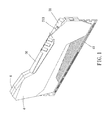
- FIG. 1 is a perspective drawing of an electronic device of a preferred embodiment of the present invention
- FIG. 2 is a breakdown drawing of the electronic device of the preferred embodiment of the present invention.
- FIG. 3 is a drawing showing a combination of a circuit module and a circuit board device of the preferred embodiment of the present invention
- FIG. 4 is a block diagram showing a structural relation of the circuit module of the preferred embodiment of the present invention.
- FIG. 5 is a partially-enlarged drawing of the electronic device of the preferred embodiment of the present invention.
- a circuit module 1 is provided for being electrically connected with a circuit board device 40 , the circuit board device 40 includes a power output portion 200 , and the circuit module 1 includes a board 10 , a boosting circuit 20 , a processing unit 24 and a plasma tube 30 .
- the boosting circuit 20 can transfer a low-voltage power input from the circuit board device 40 or a frequency changing power from the processing unit 24 into a high-voltage alternating current or a high-voltage pulsed direct current for the plasma tube 30 to use to emit a plurality of flashing lightning.
- the board 10 is provided for being connected with the circuit board device 40 with thicknesswise sides of the board 10 and the circuit board device 40 opposite to each other. It is understandable that the board and the circuit board device may be integrally formed.
- the boosting circuit 20 is disposed on the board 10 , and the boosting circuit 20 includes at least one conductive path and a plurality of electronic components 202 which are electrically connected with the at least one conductive path.
- the at least one conductive path includes a power input portion 201 for being electrically connected with the power output portion 200 and two power output terminals 23 .
- the conductive path is buried in the board 10 .
- the board 10 and the conductive path form a printed circuit board, and the conductive path may be disposed on the board in other ways.
- the boosting circuit 20 can transfer a low-voltage direct current input from the power input portion 201 into the high-voltage alternating current, and then the high-voltage alternating current is transferred through the two power output terminals 23 to the plasma tube 30 . It is understandable that the boosting circuit 20 can also transfer the low-voltage direct current into the high-voltage pulsed direct current.
- the power input portion 201 is provided for being electrically connected with a memory (the circuit board device 40 ) which is formed with the power output portion 200 , and of course, the power input portion may also be electrically connected with a display card, a network card or a printed circuit board which is formed with the power output portion.
- the board 10 has at least one through hole 100 for at least one said electronic component 202 to be disposed therewithin to decrease a thickness of the circuit module 1 .
- the board 10 has the plurality of through holes 100 so that a portion of each said electronic component 202 can be disposed within each said through hole 100 .
- the board may have only one through hole, and a plurality of electronic components are disposed therewithin; or the board may have only one through hole, and an electronic component which occupies greater space is inserted therein.
- the board may be formed without any through hole, and the electronic component can be welded on the board directly like a traditional circuit board.
- the plurality of electronic components 202 include a plurality of passive components 210 and at least one transformer 220 .
- the plurality of passive components 210 are electrically connected with one another to form a low-voltage boosting circuit 21 which is electrically connected with the power input portion 201 and the processing unit 24 so that the low-voltage boosting circuit 21 can transfer a power supplied by the circuit board device 40 into an alternating current or a pulsed direct current.
- the at least one transformer 220 forms a high-voltage boosting circuit 22 which is electrically connected with between the low-voltage boosting circuit 21 and the two power output terminals 23 , and the high-voltage boosting circuit 22 can transfer a low-voltage power into a high-voltage power for the plasma tube 30 to use.
- the plurality of electronic components 202 only have one said transformer 220 ; but in other embodiments, the plurality of electronic components 202 may have a plurality of transformers, and through the processing unit, different pins output signals to make different transformers output different voltages and produce various light fluctuation.
- the processing unit 24 is disposed on the board 10 , and the processing unit 24 includes a frequency changing circuit 240 which is electrically connected with the power input portion 201 and the boosting circuit 20 .
- a frequency changing circuit 240 Through the frequency changing circuit 240 , a input power having a first frequency input from the power input portion 201 can be transferred into an output power having a second frequency, the output power having the second frequency is transmitted to the boosting circuit 20 .
- the first and second frequencies are different.
- the boosting circuit 20 can receive a power input from the power input portion 201 and a power input from the frequency changing circuit 240 and transfer two said powers into a high-voltage pulsed direct current or a high-voltage alternating current having a predetermined frequency to be output to the two power output terminals 23 .
- the frequency changing circuit may transfer an input power having a first frequency into an output power having at least two different frequencies and transmit the output power through different pins of the processing unit to the boosting circuit; and of course, the power having different frequencies may be transmitted through a same pin in a predetermined sequence to the boosting circuit.
- the processing unit can transfer not only frequency but also voltage so as to alter a wave form of the output power and make the plasma tube produce various light fluctuation.
- each said electrode 31 includes an electrode cap 310 which is located in the plasma tube 30 and is hollow, and the two electrode caps 310 are substantially coaxially arranged; therefore, rays can be projected out along a circumferential edge of the electrode caps 310 and scattered (as shown in FIG. 5 ). Compared with a concentrated ray produced by a traditional electrode, the scattered rays are more pleasing to the eye.
- An electronic device 2 is further provided, including an above-mentioned circuit module 1 , further including a circuit board device 40 which is electrically connected with the circuit module 1 .
- the circuit board device 40 is connected with the board 10 of the circuit module 1 with thicknesswise sides of the board 10 and the circuit board device 40 opposite to each other.
- the circuit board device 40 is a memory
- the circuit board device may be a display card, a network card or a printed circuit board
- the board of the circuit module and the circuit board device may be integrally formed.
- the circuit board device 40 further includes an electric insert row 41 which is for being inserted into an electric insert slot of a computer mother board, and the electric insert row 41 is arranged on a side of the circuit board device 40 opposite to the circuit module 1 .
- the electric insert row 41 may be an insert row which matches Peripheral Component Interconnect (PCI), Peripheral Component Interconnect Express (PCI-E) or other connection interfaces so as to transfer data between the circuit board device 40 and the computer mother board through the electric insert row 41 .
- PCI Peripheral Component Interconnect
- PCI-E Peripheral Component Interconnect Express
- At least one bridging member 42 is further connected with between the circuit board device 40 and the board 10 of the circuit module 1 , each said bridging member 42 is arranged across the thicknesswise sides of the circuit board device 40 and the board 10 of the circuit module 1 , and two ends of each said bridging member 42 are fixedly connected to the circuit board device 40 and the board 10 of the circuit module 1 respectively. It is understandable that a portion of the bridging member 42 can serve as a conductive path for transferring a power of the circuit board device 40 to the circuit module 1 .
- the electronic device 2 further includes two heat-dissipating sheets 3 , and the two heat-dissipating sheets 3 are covered on two opposite sides of the electronic device 2 .
- the two heat-dissipating sheets 3 are respectively covered on a face of the circuit board device 40 so that heat produced during an operating process of the circuit board device 40 can be emitted out to prevent the electronic device 2 from being nonfunctional or damaged because of overheating.
- the electronic device 2 may be optionally formed with the heat-dissipating sheet.
- the electronic device 2 further includes at least one shell 4 , and the shell 4 is engagedly connected with one of the heat-dissipating sheets 3 substantially in parallel on a side of the electronic device 2 .
- the electronic device 2 includes two said shells 4 , and most part of the circuit module 1 and the circuit board device 40 are covered by the two shells 4 and the two heat-dissipating sheets 3 to prevent the circuit module 1 and the circuit board device 40 from being damaged.
- the shell may be made of a heat-dissipatable material so that the shell can dissipate heat.
- the heat-dissipating sheet and the shell may be integrally formed and have the effect of decoration, protection and heat-dissipation.
- the plasma tube of the present invention emit flashing lightning which is more comfortable to the user compared with the light of a light-emitting diode.
- the processing unit can produce the output power having different frequencies to be transferred through the boosting circuit, and the power output terminal outputs the power in different waveforms so as to make the plasma tube produce various light fluctuation.
Landscapes
- Engineering & Computer Science (AREA)
- Theoretical Computer Science (AREA)
- Physics & Mathematics (AREA)
- General Physics & Mathematics (AREA)
- General Engineering & Computer Science (AREA)
- Computer Hardware Design (AREA)
- Human Computer Interaction (AREA)
- Mathematical Physics (AREA)
- Quality & Reliability (AREA)
- Devices For Indicating Variable Information By Combining Individual Elements (AREA)
- Combinations Of Printed Boards (AREA)
- Microelectronics & Electronic Packaging (AREA)
Abstract
Description
Claims (10)
Applications Claiming Priority (3)
| Application Number | Priority Date | Filing Date | Title |
|---|---|---|---|
| TW104101850 | 2015-01-20 | ||
| TW104101850A TWI519050B (en) | 2015-01-20 | 2015-01-20 | Electronic device and circuit module thereof |
| TW104101850A | 2015-01-20 |
Publications (2)
| Publication Number | Publication Date |
|---|---|
| US20160212825A1 US20160212825A1 (en) | 2016-07-21 |
| US9820366B2 true US9820366B2 (en) | 2017-11-14 |
Family
ID=53935162
Family Applications (1)
| Application Number | Title | Priority Date | Filing Date |
|---|---|---|---|
| US14/884,017 Expired - Fee Related US9820366B2 (en) | 2015-01-20 | 2015-10-15 | Electronic device and circuit module thereof |
Country Status (2)
| Country | Link |
|---|---|
| US (1) | US9820366B2 (en) |
| TW (1) | TWI519050B (en) |
Cited By (4)
| Publication number | Priority date | Publication date | Assignee | Title |
|---|---|---|---|---|
| US20180024285A1 (en) * | 2016-07-22 | 2018-01-25 | Apacer Technology Inc. | Expansion card with homogenized light output and light-homogenizing device thereof |
| US9976737B2 (en) * | 2016-10-25 | 2018-05-22 | Alson Technology Limited | Computer case |
| US10465901B1 (en) * | 2018-11-02 | 2019-11-05 | Evga Corporation | Light-emitting chassis structure |
| US11157048B2 (en) * | 2018-12-03 | 2021-10-26 | Gaga-Byte Technology Co., Ltd. | Memory module with screen and motherboard module |
Families Citing this family (10)
| Publication number | Priority date | Publication date | Assignee | Title |
|---|---|---|---|---|
| TWI519050B (en) * | 2015-01-20 | 2016-01-21 | 宇帷國際股份有限公司 | Electronic device and circuit module thereof |
| US10429568B2 (en) * | 2015-10-30 | 2019-10-01 | Alson Technology Limited | Dynamic random access memory |
| US20170123136A1 (en) * | 2015-10-30 | 2017-05-04 | Avexir Technologies Corporation | Dynamic random access memory |
| TWI630479B (en) * | 2015-12-30 | 2018-07-21 | 英信科技有限公司 | System for alternating lighting of pci-e strip |
| US9723697B1 (en) * | 2016-01-27 | 2017-08-01 | Alson Technology Limited | System for alternating light-emitting of dynamic random access memory |
| EP3211506A1 (en) * | 2016-02-24 | 2017-08-30 | Avexir Technologies Corporation | Electronic device and circuit module thereof |
| TWI592057B (en) | 2016-05-30 | 2017-07-11 | 宇瞻科技股份有限公司 | Light-Emitting Device and Control Method Thereof |
| TWI632455B (en) * | 2017-03-03 | 2018-08-11 | 宇瞻科技股份有限公司 | Heat dissipation device having adjustable reflector member |
| TWI632456B (en) * | 2017-03-03 | 2018-08-11 | 宇瞻科技股份有限公司 | Reflective heat dissipation device |
| TWI654521B (en) * | 2018-04-26 | 2019-03-21 | 技嘉科技股份有限公司 | Lighting fake card module |
Citations (28)
| Publication number | Priority date | Publication date | Assignee | Title |
|---|---|---|---|---|
| US4805175A (en) * | 1987-12-03 | 1989-02-14 | Metrologic Instrumetns, Inc. | Ultra-compact, hand-held laser scanner |
| US4860194A (en) * | 1985-06-04 | 1989-08-22 | Plus Development Corporation | A method for using a modular unitary disk file subsystem |
| US4864468A (en) * | 1986-11-10 | 1989-09-05 | Bicc-Vero Electronics Gmbh | Enclosure forming housing rear wall for receiving electrical assemblies |
| US4970461A (en) * | 1989-06-26 | 1990-11-13 | Lepage Andrew J | Method and apparatus for non-contact opens/shorts testing of electrical circuits |
| US5032788A (en) * | 1989-06-26 | 1991-07-16 | Digital Equipment Corp. | Test cell for non-contact opens/shorts testing of electrical circuits |
| US5036481A (en) * | 1989-04-18 | 1991-07-30 | Dell Usa Corporation | Personal computer system with dual purpose expansion slot |
| US5557506A (en) * | 1995-03-31 | 1996-09-17 | Alantec | Expandable data processing chassis and method of assembly thereof |
| US5816859A (en) * | 1995-10-13 | 1998-10-06 | Texas Microsystems, Inc. | Separable wire terminus connector mounting assembly system for use with computers |
| US6348277B1 (en) * | 1997-10-06 | 2002-02-19 | Reveo, Inc. | Method of and system for producing and supplying electrical power to an electrical power consuming device using a metal-air fuel cell battery (FCB) module and a supply of metal-fuel cards |
| US6644866B1 (en) * | 1998-09-01 | 2003-11-11 | Fujitsu Limited | Electronic apparatus |
| US6655814B1 (en) * | 1999-10-15 | 2003-12-02 | Tadahiro Tagawa | Light emitting block |
| TWM263537U (en) | 2004-08-31 | 2005-05-01 | Wei Heh Electronics Corp | Electrical connecting board capable of recognizing quality of plug-in units |
| US6988026B2 (en) * | 1995-06-07 | 2006-01-17 | Automotive Technologies International Inc. | Wireless and powerless sensor and interrogator |
| US7154174B2 (en) * | 2003-02-27 | 2006-12-26 | Power-One, Inc. | Power supply packaging system |
| US20090128471A1 (en) * | 2007-11-15 | 2009-05-21 | Young Lighting Technology Corporation | Integrated driving board and liquid crystal display module having the same |
| US20110211061A1 (en) * | 1999-06-15 | 2011-09-01 | Tessera International, Inc. | Sealed, waterproof digital electronic camera system and method of fabricating same |
| US20110273906A1 (en) * | 2010-04-16 | 2011-11-10 | Anthony John Nichol | Front illumination device comprising a film-based lightguide |
| US20130155723A1 (en) * | 2009-01-26 | 2013-06-20 | Flex Lighting Ii, Llc | Replaceable lightguide film display |
| US20130310171A1 (en) * | 2012-05-18 | 2013-11-21 | Aruze Gaming America, Inc. | Display device for gaming machine and gaming machine including the same |
| US20140071032A1 (en) * | 2008-12-19 | 2014-03-13 | Semiconductor Energy Laboratory Co., Ltd. | Method for driving liquid crystal display device |
| US8988867B2 (en) * | 2010-06-24 | 2015-03-24 | Sharp Kabushiki Kaisha | Display device and television receiver |
| US9013367B2 (en) * | 2008-01-04 | 2015-04-21 | Nanolumens Acquisition Inc. | Flexible display |
| US9058755B2 (en) * | 2008-01-04 | 2015-06-16 | Nanolumens Acquisition, Inc. | Lightweight unitary display |
| US20150317121A1 (en) * | 2008-01-04 | 2015-11-05 | Nanolumens Acquisition, Inc, | Mobile, Personsize Display System and Method of Use |
| US9326620B1 (en) * | 2015-03-12 | 2016-05-03 | Nanolumens Acquisition, Inc. | Modular display system and methods |
| US20160212825A1 (en) * | 2015-01-20 | 2016-07-21 | Avexir Technologies Corporation | Electronic device and circuit module thereof |
| US20160212824A1 (en) * | 2015-01-20 | 2016-07-21 | Avexir Technologies Corporation | Electronic device and circuit module thereof |
| US9543636B2 (en) * | 2013-01-15 | 2017-01-10 | Fitbit, Inc. | Hybrid radio frequency/inductive loop charger |
-
2015
- 2015-01-20 TW TW104101850A patent/TWI519050B/en not_active IP Right Cessation
- 2015-10-15 US US14/884,017 patent/US9820366B2/en not_active Expired - Fee Related
Patent Citations (33)
| Publication number | Priority date | Publication date | Assignee | Title |
|---|---|---|---|---|
| US4860194A (en) * | 1985-06-04 | 1989-08-22 | Plus Development Corporation | A method for using a modular unitary disk file subsystem |
| US4864468A (en) * | 1986-11-10 | 1989-09-05 | Bicc-Vero Electronics Gmbh | Enclosure forming housing rear wall for receiving electrical assemblies |
| US4805175A (en) * | 1987-12-03 | 1989-02-14 | Metrologic Instrumetns, Inc. | Ultra-compact, hand-held laser scanner |
| US5036481A (en) * | 1989-04-18 | 1991-07-30 | Dell Usa Corporation | Personal computer system with dual purpose expansion slot |
| US4970461A (en) * | 1989-06-26 | 1990-11-13 | Lepage Andrew J | Method and apparatus for non-contact opens/shorts testing of electrical circuits |
| US5032788A (en) * | 1989-06-26 | 1991-07-16 | Digital Equipment Corp. | Test cell for non-contact opens/shorts testing of electrical circuits |
| US5557506A (en) * | 1995-03-31 | 1996-09-17 | Alantec | Expandable data processing chassis and method of assembly thereof |
| US5689406A (en) * | 1995-03-31 | 1997-11-18 | Alantec | Expandable data processing chassis and method of assembly thereof |
| US6988026B2 (en) * | 1995-06-07 | 2006-01-17 | Automotive Technologies International Inc. | Wireless and powerless sensor and interrogator |
| US5816859A (en) * | 1995-10-13 | 1998-10-06 | Texas Microsystems, Inc. | Separable wire terminus connector mounting assembly system for use with computers |
| US6348277B1 (en) * | 1997-10-06 | 2002-02-19 | Reveo, Inc. | Method of and system for producing and supplying electrical power to an electrical power consuming device using a metal-air fuel cell battery (FCB) module and a supply of metal-fuel cards |
| US6644866B1 (en) * | 1998-09-01 | 2003-11-11 | Fujitsu Limited | Electronic apparatus |
| US20110211061A1 (en) * | 1999-06-15 | 2011-09-01 | Tessera International, Inc. | Sealed, waterproof digital electronic camera system and method of fabricating same |
| US6655814B1 (en) * | 1999-10-15 | 2003-12-02 | Tadahiro Tagawa | Light emitting block |
| US7154174B2 (en) * | 2003-02-27 | 2006-12-26 | Power-One, Inc. | Power supply packaging system |
| TWM263537U (en) | 2004-08-31 | 2005-05-01 | Wei Heh Electronics Corp | Electrical connecting board capable of recognizing quality of plug-in units |
| US20090128471A1 (en) * | 2007-11-15 | 2009-05-21 | Young Lighting Technology Corporation | Integrated driving board and liquid crystal display module having the same |
| US20150247627A1 (en) * | 2008-01-04 | 2015-09-03 | Nanolumens Acquisition, Inc, | Lightweight Unitary Display |
| US20160371047A1 (en) * | 2008-01-04 | 2016-12-22 | NanoLumens Acquisition, Inc | Lightweight Unitary Display |
| US20150317121A1 (en) * | 2008-01-04 | 2015-11-05 | Nanolumens Acquisition, Inc, | Mobile, Personsize Display System and Method of Use |
| US9159707B2 (en) * | 2008-01-04 | 2015-10-13 | Nanolumens Acquisition, Inc. | Flexible display |
| US9013367B2 (en) * | 2008-01-04 | 2015-04-21 | Nanolumens Acquisition Inc. | Flexible display |
| US9058755B2 (en) * | 2008-01-04 | 2015-06-16 | Nanolumens Acquisition, Inc. | Lightweight unitary display |
| US20150214195A1 (en) * | 2008-01-04 | 2015-07-30 | Nanolumens Acquisition, Inc, | Flexible Display |
| US20140071032A1 (en) * | 2008-12-19 | 2014-03-13 | Semiconductor Energy Laboratory Co., Ltd. | Method for driving liquid crystal display device |
| US20130155723A1 (en) * | 2009-01-26 | 2013-06-20 | Flex Lighting Ii, Llc | Replaceable lightguide film display |
| US20110273906A1 (en) * | 2010-04-16 | 2011-11-10 | Anthony John Nichol | Front illumination device comprising a film-based lightguide |
| US8988867B2 (en) * | 2010-06-24 | 2015-03-24 | Sharp Kabushiki Kaisha | Display device and television receiver |
| US20130310171A1 (en) * | 2012-05-18 | 2013-11-21 | Aruze Gaming America, Inc. | Display device for gaming machine and gaming machine including the same |
| US9543636B2 (en) * | 2013-01-15 | 2017-01-10 | Fitbit, Inc. | Hybrid radio frequency/inductive loop charger |
| US20160212825A1 (en) * | 2015-01-20 | 2016-07-21 | Avexir Technologies Corporation | Electronic device and circuit module thereof |
| US20160212824A1 (en) * | 2015-01-20 | 2016-07-21 | Avexir Technologies Corporation | Electronic device and circuit module thereof |
| US9326620B1 (en) * | 2015-03-12 | 2016-05-03 | Nanolumens Acquisition, Inc. | Modular display system and methods |
Cited By (5)
| Publication number | Priority date | Publication date | Assignee | Title |
|---|---|---|---|---|
| US20180024285A1 (en) * | 2016-07-22 | 2018-01-25 | Apacer Technology Inc. | Expansion card with homogenized light output and light-homogenizing device thereof |
| US10288791B2 (en) * | 2016-07-22 | 2019-05-14 | Apacer Technology Inc. | Expansion card with homogenized light output and light-homogenizing device thereof |
| US9976737B2 (en) * | 2016-10-25 | 2018-05-22 | Alson Technology Limited | Computer case |
| US10465901B1 (en) * | 2018-11-02 | 2019-11-05 | Evga Corporation | Light-emitting chassis structure |
| US11157048B2 (en) * | 2018-12-03 | 2021-10-26 | Gaga-Byte Technology Co., Ltd. | Memory module with screen and motherboard module |
Also Published As
| Publication number | Publication date |
|---|---|
| US20160212825A1 (en) | 2016-07-21 |
| TW201521346A (en) | 2015-06-01 |
| TWI519050B (en) | 2016-01-21 |
Similar Documents
| Publication | Publication Date | Title |
|---|---|---|
| US9820366B2 (en) | Electronic device and circuit module thereof | |
| US9795018B2 (en) | Electronic device and circuit module thereof | |
| US9817168B2 (en) | Circuit module | |
| AU2008326437B2 (en) | Apparatus for housing a light assembly | |
| US9450350B2 (en) | Cable connector assembly with improved luminous effect | |
| CN105190169B (en) | Lighting apparatus | |
| US9863624B2 (en) | Gas-filled LED bulb manufactured by SMT | |
| ES2193868B1 (en) | SET OF FUSE ELEMENTS FOR A COMPLETE RANGE FUSE. | |
| EP3211506A1 (en) | Electronic device and circuit module thereof | |
| EP3705772B1 (en) | Intelligent lamp including light source module and communications module | |
| CN105570700A (en) | Lighting device | |
| RU2014151164A (en) | ANTENNA WITH MULTI-CHANNEL INPUT AND MULTI-CHANNEL OUTPUT AND ELECTRONIC EQUIPMENT | |
| EP3247185A1 (en) | Heat dissipation apparatus for small-size device and circuit board heat dissipation system | |
| CN104597978A (en) | Electronic device and circuit module thereof | |
| US20180136710A1 (en) | Power supply device | |
| US10349474B2 (en) | Lamp tube capable of rectifying and stabilizing voltages | |
| US9976737B2 (en) | Computer case | |
| KR20110000835A (en) | Emi shielding case and led illumination device including the case | |
| WO2019029660A1 (en) | Pin-based light bulb | |
| US20180083382A1 (en) | An adapter | |
| CN217684882U (en) | Circuit board module and lamp | |
| US20150159815A1 (en) | Direct-type illumination device and light bar structure for use therein | |
| TW201813476A (en) | Computer case | |
| WO2016138680A1 (en) | Light-emitting element package and display device | |
| CN203350776U (en) | Circuit module |
Legal Events
| Date | Code | Title | Description |
|---|---|---|---|
| AS | Assignment |
Owner name: AVEXIR TECHNOLOGIES CORPORATION, TAIWAN Free format text: ASSIGNMENT OF ASSIGNORS INTEREST;ASSIGNORS:KUO, CHI-FEN;CHENG, HAN-HUNG;REEL/FRAME:036801/0673 Effective date: 20151013 |
|
| AS | Assignment |
Owner name: ALSON TECHNOLOGY LIMITED, HONG KONG Free format text: ASSIGNMENT OF ASSIGNORS INTEREST;ASSIGNOR:AVEXIR TECHNOLOGIES CORPORATION;REEL/FRAME:042041/0849 Effective date: 20170405 |
|
| STCF | Information on status: patent grant |
Free format text: PATENTED CASE |
|
| FEPP | Fee payment procedure |
Free format text: MAINTENANCE FEE REMINDER MAILED (ORIGINAL EVENT CODE: REM.); ENTITY STATUS OF PATENT OWNER: SMALL ENTITY |
|
| LAPS | Lapse for failure to pay maintenance fees |
Free format text: PATENT EXPIRED FOR FAILURE TO PAY MAINTENANCE FEES (ORIGINAL EVENT CODE: EXP.); ENTITY STATUS OF PATENT OWNER: SMALL ENTITY |
|
| STCH | Information on status: patent discontinuation |
Free format text: PATENT EXPIRED DUE TO NONPAYMENT OF MAINTENANCE FEES UNDER 37 CFR 1.362 |
|
| FP | Lapsed due to failure to pay maintenance fee |
Effective date: 20211114 |