US9852904B2 - Method for manufacturing semiconductor device - Google Patents
Method for manufacturing semiconductor device Download PDFInfo
- Publication number
- US9852904B2 US9852904B2 US14/813,413 US201514813413A US9852904B2 US 9852904 B2 US9852904 B2 US 9852904B2 US 201514813413 A US201514813413 A US 201514813413A US 9852904 B2 US9852904 B2 US 9852904B2
- Authority
- US
- United States
- Prior art keywords
- electrode layer
- insulating film
- transistor
- film
- oxide semiconductor
- Prior art date
- Legal status (The legal status is an assumption and is not a legal conclusion. Google has not performed a legal analysis and makes no representation as to the accuracy of the status listed.)
- Active
Links
- 239000004065 semiconductor Substances 0.000 title claims abstract description 309
- 238000000034 method Methods 0.000 title claims abstract description 66
- 238000004519 manufacturing process Methods 0.000 title claims description 32
- QVGXLLKOCUKJST-UHFFFAOYSA-N atomic oxygen Chemical compound [O] QVGXLLKOCUKJST-UHFFFAOYSA-N 0.000 claims abstract description 147
- 239000001301 oxygen Substances 0.000 claims abstract description 145
- 229910052760 oxygen Inorganic materials 0.000 claims abstract description 145
- 238000005468 ion implantation Methods 0.000 claims abstract description 11
- 230000001681 protective effect Effects 0.000 claims description 44
- 239000000463 material Substances 0.000 claims description 42
- 229910052721 tungsten Inorganic materials 0.000 claims description 39
- NRTOMJZYCJJWKI-UHFFFAOYSA-N Titanium nitride Chemical compound [Ti]#N NRTOMJZYCJJWKI-UHFFFAOYSA-N 0.000 claims description 37
- MZLGASXMSKOWSE-UHFFFAOYSA-N tantalum nitride Chemical compound [Ta]#N MZLGASXMSKOWSE-UHFFFAOYSA-N 0.000 claims description 20
- 238000005530 etching Methods 0.000 claims description 12
- 229910052719 titanium Inorganic materials 0.000 claims description 11
- 239000010936 titanium Substances 0.000 claims description 11
- 229910052715 tantalum Inorganic materials 0.000 claims description 8
- 229910052782 aluminium Inorganic materials 0.000 claims description 7
- 229910052804 chromium Inorganic materials 0.000 claims description 6
- 229910052802 copper Inorganic materials 0.000 claims description 6
- 229910052750 molybdenum Inorganic materials 0.000 claims description 6
- 229910052707 ruthenium Inorganic materials 0.000 claims description 6
- KJTLSVCANCCWHF-UHFFFAOYSA-N Ruthenium Chemical compound [Ru] KJTLSVCANCCWHF-UHFFFAOYSA-N 0.000 claims description 4
- 238000010894 electron beam technology Methods 0.000 claims description 2
- 230000015572 biosynthetic process Effects 0.000 abstract description 35
- 239000010410 layer Substances 0.000 description 500
- 239000010408 film Substances 0.000 description 493
- 238000010438 heat treatment Methods 0.000 description 51
- 239000000758 substrate Substances 0.000 description 44
- 239000011701 zinc Substances 0.000 description 37
- 238000004544 sputter deposition Methods 0.000 description 36
- WFKWXMTUELFFGS-UHFFFAOYSA-N tungsten Chemical compound [W] WFKWXMTUELFFGS-UHFFFAOYSA-N 0.000 description 35
- 239000010937 tungsten Substances 0.000 description 35
- 239000003990 capacitor Substances 0.000 description 31
- 239000007789 gas Substances 0.000 description 31
- 239000013078 crystal Substances 0.000 description 28
- 239000000523 sample Substances 0.000 description 26
- 125000004429 atom Chemical group 0.000 description 24
- 238000000151 deposition Methods 0.000 description 24
- 230000008021 deposition Effects 0.000 description 24
- XUIMIQQOPSSXEZ-UHFFFAOYSA-N Silicon Chemical compound [Si] XUIMIQQOPSSXEZ-UHFFFAOYSA-N 0.000 description 18
- 238000004458 analytical method Methods 0.000 description 18
- 239000012535 impurity Substances 0.000 description 18
- 238000001004 secondary ion mass spectrometry Methods 0.000 description 18
- 229910052710 silicon Inorganic materials 0.000 description 17
- 239000010703 silicon Substances 0.000 description 17
- 238000005477 sputtering target Methods 0.000 description 17
- 229910052733 gallium Inorganic materials 0.000 description 15
- 229910052725 zinc Inorganic materials 0.000 description 15
- IJGRMHOSHXDMSA-UHFFFAOYSA-N Atomic nitrogen Chemical compound N#N IJGRMHOSHXDMSA-UHFFFAOYSA-N 0.000 description 14
- VYPSYNLAJGMNEJ-UHFFFAOYSA-N Silicium dioxide Chemical compound O=[Si]=O VYPSYNLAJGMNEJ-UHFFFAOYSA-N 0.000 description 14
- 229910052739 hydrogen Inorganic materials 0.000 description 14
- 239000001257 hydrogen Substances 0.000 description 14
- 230000002349 favourable effect Effects 0.000 description 13
- 230000006870 function Effects 0.000 description 13
- 229910052738 indium Inorganic materials 0.000 description 13
- 238000006243 chemical reaction Methods 0.000 description 12
- 229910052751 metal Inorganic materials 0.000 description 12
- 238000012546 transfer Methods 0.000 description 12
- UFHFLCQGNIYNRP-UHFFFAOYSA-N Hydrogen Chemical compound [H][H] UFHFLCQGNIYNRP-UHFFFAOYSA-N 0.000 description 11
- 229910052581 Si3N4 Inorganic materials 0.000 description 11
- 239000004020 conductor Substances 0.000 description 11
- HQVNEWCFYHHQES-UHFFFAOYSA-N silicon nitride Chemical compound N12[Si]34N5[Si]62N3[Si]51N64 HQVNEWCFYHHQES-UHFFFAOYSA-N 0.000 description 11
- 229910052814 silicon oxide Inorganic materials 0.000 description 11
- 239000002184 metal Substances 0.000 description 10
- 230000009467 reduction Effects 0.000 description 10
- 238000005259 measurement Methods 0.000 description 9
- 239000002245 particle Substances 0.000 description 8
- 230000008569 process Effects 0.000 description 8
- 238000005229 chemical vapour deposition Methods 0.000 description 7
- 238000010586 diagram Methods 0.000 description 7
- 150000002500 ions Chemical class 0.000 description 7
- 229910052757 nitrogen Inorganic materials 0.000 description 7
- 230000003287 optical effect Effects 0.000 description 7
- 230000002093 peripheral effect Effects 0.000 description 7
- XLOMVQKBTHCTTD-UHFFFAOYSA-N Zinc monoxide Chemical compound [Zn]=O XLOMVQKBTHCTTD-UHFFFAOYSA-N 0.000 description 6
- MRELNEQAGSRDBK-UHFFFAOYSA-N lanthanum(3+);oxygen(2-) Chemical compound [O-2].[O-2].[O-2].[La+3].[La+3] MRELNEQAGSRDBK-UHFFFAOYSA-N 0.000 description 6
- PLDDOISOJJCEMH-UHFFFAOYSA-N neodymium(3+);oxygen(2-) Chemical compound [O-2].[O-2].[O-2].[Nd+3].[Nd+3] PLDDOISOJJCEMH-UHFFFAOYSA-N 0.000 description 6
- RTAQQCXQSZGOHL-UHFFFAOYSA-N Titanium Chemical compound [Ti] RTAQQCXQSZGOHL-UHFFFAOYSA-N 0.000 description 5
- 239000000956 alloy Substances 0.000 description 5
- 230000006399 behavior Effects 0.000 description 5
- 238000002955 isolation Methods 0.000 description 5
- 230000007774 longterm Effects 0.000 description 5
- 150000004767 nitrides Chemical class 0.000 description 5
- 239000000843 powder Substances 0.000 description 5
- 238000012545 processing Methods 0.000 description 5
- 238000003917 TEM image Methods 0.000 description 4
- 239000012298 atmosphere Substances 0.000 description 4
- 238000000231 atomic layer deposition Methods 0.000 description 4
- 230000008859 change Effects 0.000 description 4
- 230000006866 deterioration Effects 0.000 description 4
- 238000009792 diffusion process Methods 0.000 description 4
- 229910052732 germanium Inorganic materials 0.000 description 4
- GNPVGFCGXDBREM-UHFFFAOYSA-N germanium atom Chemical compound [Ge] GNPVGFCGXDBREM-UHFFFAOYSA-N 0.000 description 4
- 239000000203 mixture Substances 0.000 description 4
- 238000005546 reactive sputtering Methods 0.000 description 4
- 230000000717 retained effect Effects 0.000 description 4
- GUVRBAGPIYLISA-UHFFFAOYSA-N tantalum atom Chemical compound [Ta] GUVRBAGPIYLISA-UHFFFAOYSA-N 0.000 description 4
- XLYOFNOQVPJJNP-UHFFFAOYSA-N water Substances O XLYOFNOQVPJJNP-UHFFFAOYSA-N 0.000 description 4
- 229910001868 water Inorganic materials 0.000 description 4
- 239000011787 zinc oxide Substances 0.000 description 4
- 229910018137 Al-Zn Inorganic materials 0.000 description 3
- 229910018573 Al—Zn Inorganic materials 0.000 description 3
- OKTJSMMVPCPJKN-UHFFFAOYSA-N Carbon Chemical compound [C] OKTJSMMVPCPJKN-UHFFFAOYSA-N 0.000 description 3
- CURLTUGMZLYLDI-UHFFFAOYSA-N Carbon dioxide Chemical compound O=C=O CURLTUGMZLYLDI-UHFFFAOYSA-N 0.000 description 3
- HBBGRARXTFLTSG-UHFFFAOYSA-N Lithium ion Chemical compound [Li+] HBBGRARXTFLTSG-UHFFFAOYSA-N 0.000 description 3
- 238000003491 array Methods 0.000 description 3
- 238000004380 ashing Methods 0.000 description 3
- 229910052799 carbon Inorganic materials 0.000 description 3
- 150000001875 compounds Chemical class 0.000 description 3
- 229910021419 crystalline silicon Inorganic materials 0.000 description 3
- AJNVQOSZGJRYEI-UHFFFAOYSA-N digallium;oxygen(2-) Chemical compound [O-2].[O-2].[O-2].[Ga+3].[Ga+3] AJNVQOSZGJRYEI-UHFFFAOYSA-N 0.000 description 3
- 229910001195 gallium oxide Inorganic materials 0.000 description 3
- YBMRDBCBODYGJE-UHFFFAOYSA-N germanium oxide Inorganic materials O=[Ge]=O YBMRDBCBODYGJE-UHFFFAOYSA-N 0.000 description 3
- 229910000449 hafnium oxide Inorganic materials 0.000 description 3
- WIHZLLGSGQNAGK-UHFFFAOYSA-N hafnium(4+);oxygen(2-) Chemical compound [O-2].[O-2].[Hf+4] WIHZLLGSGQNAGK-UHFFFAOYSA-N 0.000 description 3
- 150000002431 hydrogen Chemical class 0.000 description 3
- 238000007654 immersion Methods 0.000 description 3
- APFVFJFRJDLVQX-UHFFFAOYSA-N indium atom Chemical compound [In] APFVFJFRJDLVQX-UHFFFAOYSA-N 0.000 description 3
- 238000010884 ion-beam technique Methods 0.000 description 3
- 229910001416 lithium ion Inorganic materials 0.000 description 3
- CPLXHLVBOLITMK-UHFFFAOYSA-N magnesium oxide Inorganic materials [Mg]=O CPLXHLVBOLITMK-UHFFFAOYSA-N 0.000 description 3
- 239000000395 magnesium oxide Substances 0.000 description 3
- AXZKOIWUVFPNLO-UHFFFAOYSA-N magnesium;oxygen(2-) Chemical compound [O-2].[Mg+2] AXZKOIWUVFPNLO-UHFFFAOYSA-N 0.000 description 3
- 238000001451 molecular beam epitaxy Methods 0.000 description 3
- TWNQGVIAIRXVLR-UHFFFAOYSA-N oxo(oxoalumanyloxy)alumane Chemical compound O=[Al]O[Al]=O TWNQGVIAIRXVLR-UHFFFAOYSA-N 0.000 description 3
- SIWVEOZUMHYXCS-UHFFFAOYSA-N oxo(oxoyttriooxy)yttrium Chemical compound O=[Y]O[Y]=O SIWVEOZUMHYXCS-UHFFFAOYSA-N 0.000 description 3
- PVADDRMAFCOOPC-UHFFFAOYSA-N oxogermanium Chemical compound [Ge]=O PVADDRMAFCOOPC-UHFFFAOYSA-N 0.000 description 3
- 125000004430 oxygen atom Chemical group O* 0.000 description 3
- BPUBBGLMJRNUCC-UHFFFAOYSA-N oxygen(2-);tantalum(5+) Chemical compound [O-2].[O-2].[O-2].[O-2].[O-2].[Ta+5].[Ta+5] BPUBBGLMJRNUCC-UHFFFAOYSA-N 0.000 description 3
- RVTZCBVAJQQJTK-UHFFFAOYSA-N oxygen(2-);zirconium(4+) Chemical compound [O-2].[O-2].[Zr+4] RVTZCBVAJQQJTK-UHFFFAOYSA-N 0.000 description 3
- 239000003381 stabilizer Substances 0.000 description 3
- 229910001936 tantalum oxide Inorganic materials 0.000 description 3
- JBQYATWDVHIOAR-UHFFFAOYSA-N tellanylidenegermanium Chemical compound [Te]=[Ge] JBQYATWDVHIOAR-UHFFFAOYSA-N 0.000 description 3
- 239000010409 thin film Substances 0.000 description 3
- 229910001928 zirconium oxide Inorganic materials 0.000 description 3
- 229910018120 Al-Ga-Zn Inorganic materials 0.000 description 2
- QGZKDVFQNNGYKY-UHFFFAOYSA-N Ammonia Chemical compound N QGZKDVFQNNGYKY-UHFFFAOYSA-N 0.000 description 2
- 102100040844 Dual specificity protein kinase CLK2 Human genes 0.000 description 2
- GYHNNYVSQQEPJS-UHFFFAOYSA-N Gallium Chemical compound [Ga] GYHNNYVSQQEPJS-UHFFFAOYSA-N 0.000 description 2
- 101000749291 Homo sapiens Dual specificity protein kinase CLK2 Proteins 0.000 description 2
- 229910000577 Silicon-germanium Inorganic materials 0.000 description 2
- 229910020833 Sn-Al-Zn Inorganic materials 0.000 description 2
- 229910020868 Sn-Ga-Zn Inorganic materials 0.000 description 2
- 229910020994 Sn-Zn Inorganic materials 0.000 description 2
- 229910009069 Sn—Zn Inorganic materials 0.000 description 2
- 229910007541 Zn O Inorganic materials 0.000 description 2
- LEVVHYCKPQWKOP-UHFFFAOYSA-N [Si].[Ge] Chemical compound [Si].[Ge] LEVVHYCKPQWKOP-UHFFFAOYSA-N 0.000 description 2
- 230000002159 abnormal effect Effects 0.000 description 2
- 229910002092 carbon dioxide Inorganic materials 0.000 description 2
- 238000002485 combustion reaction Methods 0.000 description 2
- 239000011521 glass Substances 0.000 description 2
- QOSATHPSBFQAML-UHFFFAOYSA-N hydrogen peroxide;hydrate Chemical compound O.OO QOSATHPSBFQAML-UHFFFAOYSA-N 0.000 description 2
- 239000011261 inert gas Substances 0.000 description 2
- 230000010354 integration Effects 0.000 description 2
- 230000005012 migration Effects 0.000 description 2
- 238000013508 migration Methods 0.000 description 2
- 238000002156 mixing Methods 0.000 description 2
- 229910052759 nickel Inorganic materials 0.000 description 2
- 239000012299 nitrogen atmosphere Substances 0.000 description 2
- 230000001590 oxidative effect Effects 0.000 description 2
- -1 oxygen ion Chemical class 0.000 description 2
- 230000003071 parasitic effect Effects 0.000 description 2
- 238000000206 photolithography Methods 0.000 description 2
- HBMJWWWQQXIZIP-UHFFFAOYSA-N silicon carbide Chemical compound [Si+]#[C-] HBMJWWWQQXIZIP-UHFFFAOYSA-N 0.000 description 2
- 229910010271 silicon carbide Inorganic materials 0.000 description 2
- 239000000779 smoke Substances 0.000 description 2
- 238000003860 storage Methods 0.000 description 2
- 229910052727 yttrium Inorganic materials 0.000 description 2
- 229910052726 zirconium Inorganic materials 0.000 description 2
- JBRZTFJDHDCESZ-UHFFFAOYSA-N AsGa Chemical compound [As]#[Ga] JBRZTFJDHDCESZ-UHFFFAOYSA-N 0.000 description 1
- 229910052684 Cerium Inorganic materials 0.000 description 1
- 102100040862 Dual specificity protein kinase CLK1 Human genes 0.000 description 1
- 229910052692 Dysprosium Inorganic materials 0.000 description 1
- 229910052691 Erbium Inorganic materials 0.000 description 1
- 229910052693 Europium Inorganic materials 0.000 description 1
- 229910052688 Gadolinium Inorganic materials 0.000 description 1
- 229910001218 Gallium arsenide Inorganic materials 0.000 description 1
- 235000015842 Hesperis Nutrition 0.000 description 1
- 229910052689 Holmium Inorganic materials 0.000 description 1
- 101000749294 Homo sapiens Dual specificity protein kinase CLK1 Proteins 0.000 description 1
- 235000012633 Iberis amara Nutrition 0.000 description 1
- 229910052765 Lutetium Inorganic materials 0.000 description 1
- 229910052779 Neodymium Inorganic materials 0.000 description 1
- 240000007594 Oryza sativa Species 0.000 description 1
- 235000007164 Oryza sativa Nutrition 0.000 description 1
- CBENFWSGALASAD-UHFFFAOYSA-N Ozone Chemical compound [O-][O+]=O CBENFWSGALASAD-UHFFFAOYSA-N 0.000 description 1
- 229910052777 Praseodymium Inorganic materials 0.000 description 1
- 229910052772 Samarium Inorganic materials 0.000 description 1
- 241001591005 Siga Species 0.000 description 1
- 229910020944 Sn-Mg Inorganic materials 0.000 description 1
- 229910052771 Terbium Inorganic materials 0.000 description 1
- 229910052775 Thulium Inorganic materials 0.000 description 1
- ATJFFYVFTNAWJD-UHFFFAOYSA-N Tin Chemical compound [Sn] ATJFFYVFTNAWJD-UHFFFAOYSA-N 0.000 description 1
- 229910052769 Ytterbium Inorganic materials 0.000 description 1
- 229910009369 Zn Mg Inorganic materials 0.000 description 1
- 229910007573 Zn-Mg Inorganic materials 0.000 description 1
- 238000010521 absorption reaction Methods 0.000 description 1
- 230000001133 acceleration Effects 0.000 description 1
- 238000009825 accumulation Methods 0.000 description 1
- 238000004378 air conditioning Methods 0.000 description 1
- XAGFODPZIPBFFR-UHFFFAOYSA-N aluminium Chemical compound [Al] XAGFODPZIPBFFR-UHFFFAOYSA-N 0.000 description 1
- 229910021529 ammonia Inorganic materials 0.000 description 1
- 230000005540 biological transmission Effects 0.000 description 1
- 239000001569 carbon dioxide Substances 0.000 description 1
- 239000000919 ceramic Substances 0.000 description 1
- GWXLDORMOJMVQZ-UHFFFAOYSA-N cerium Chemical compound [Ce] GWXLDORMOJMVQZ-UHFFFAOYSA-N 0.000 description 1
- 229910052681 coesite Inorganic materials 0.000 description 1
- 229910052906 cristobalite Inorganic materials 0.000 description 1
- 238000002425 crystallisation Methods 0.000 description 1
- 230000008025 crystallization Effects 0.000 description 1
- 230000003247 decreasing effect Effects 0.000 description 1
- 230000007547 defect Effects 0.000 description 1
- 238000003795 desorption Methods 0.000 description 1
- 238000009826 distribution Methods 0.000 description 1
- 239000000428 dust Substances 0.000 description 1
- KBQHZAAAGSGFKK-UHFFFAOYSA-N dysprosium atom Chemical compound [Dy] KBQHZAAAGSGFKK-UHFFFAOYSA-N 0.000 description 1
- UYAHIZSMUZPPFV-UHFFFAOYSA-N erbium Chemical compound [Er] UYAHIZSMUZPPFV-UHFFFAOYSA-N 0.000 description 1
- OGPBJKLSAFTDLK-UHFFFAOYSA-N europium atom Chemical compound [Eu] OGPBJKLSAFTDLK-UHFFFAOYSA-N 0.000 description 1
- 239000000284 extract Substances 0.000 description 1
- 230000005669 field effect Effects 0.000 description 1
- UIWYJDYFSGRHKR-UHFFFAOYSA-N gadolinium atom Chemical compound [Gd] UIWYJDYFSGRHKR-UHFFFAOYSA-N 0.000 description 1
- 229910052735 hafnium Inorganic materials 0.000 description 1
- VBJZVLUMGGDVMO-UHFFFAOYSA-N hafnium atom Chemical compound [Hf] VBJZVLUMGGDVMO-UHFFFAOYSA-N 0.000 description 1
- KJZYNXUDTRRSPN-UHFFFAOYSA-N holmium atom Chemical compound [Ho] KJZYNXUDTRRSPN-UHFFFAOYSA-N 0.000 description 1
- 238000002513 implantation Methods 0.000 description 1
- 229910003437 indium oxide Inorganic materials 0.000 description 1
- PJXISJQVUVHSOJ-UHFFFAOYSA-N indium(iii) oxide Chemical compound [O-2].[O-2].[O-2].[In+3].[In+3] PJXISJQVUVHSOJ-UHFFFAOYSA-N 0.000 description 1
- 239000012212 insulator Substances 0.000 description 1
- 239000011229 interlayer Substances 0.000 description 1
- 229910000765 intermetallic Inorganic materials 0.000 description 1
- 229910052742 iron Inorganic materials 0.000 description 1
- 229910052747 lanthanoid Inorganic materials 0.000 description 1
- 150000002602 lanthanoids Chemical class 0.000 description 1
- 229910052746 lanthanum Inorganic materials 0.000 description 1
- FZLIPJUXYLNCLC-UHFFFAOYSA-N lanthanum atom Chemical compound [La] FZLIPJUXYLNCLC-UHFFFAOYSA-N 0.000 description 1
- OHSVLFRHMCKCQY-UHFFFAOYSA-N lutetium atom Chemical compound [Lu] OHSVLFRHMCKCQY-UHFFFAOYSA-N 0.000 description 1
- 239000011777 magnesium Substances 0.000 description 1
- 229910052748 manganese Inorganic materials 0.000 description 1
- 238000002844 melting Methods 0.000 description 1
- 230000008018 melting Effects 0.000 description 1
- 239000011259 mixed solution Substances 0.000 description 1
- 229910021421 monocrystalline silicon Inorganic materials 0.000 description 1
- QEFYFXOXNSNQGX-UHFFFAOYSA-N neodymium atom Chemical compound [Nd] QEFYFXOXNSNQGX-UHFFFAOYSA-N 0.000 description 1
- QJGQUHMNIGDVPM-UHFFFAOYSA-N nitrogen group Chemical group [N] QJGQUHMNIGDVPM-UHFFFAOYSA-N 0.000 description 1
- 239000003921 oil Substances 0.000 description 1
- 230000003647 oxidation Effects 0.000 description 1
- 238000007254 oxidation reaction Methods 0.000 description 1
- 238000005498 polishing Methods 0.000 description 1
- PUDIUYLPXJFUGB-UHFFFAOYSA-N praseodymium atom Chemical compound [Pr] PUDIUYLPXJFUGB-UHFFFAOYSA-N 0.000 description 1
- 238000003825 pressing Methods 0.000 description 1
- 239000010453 quartz Substances 0.000 description 1
- 230000005855 radiation Effects 0.000 description 1
- 238000001552 radio frequency sputter deposition Methods 0.000 description 1
- 235000009566 rice Nutrition 0.000 description 1
- KZUNJOHGWZRPMI-UHFFFAOYSA-N samarium atom Chemical compound [Sm] KZUNJOHGWZRPMI-UHFFFAOYSA-N 0.000 description 1
- 229910052594 sapphire Inorganic materials 0.000 description 1
- 239000010980 sapphire Substances 0.000 description 1
- VSZWPYCFIRKVQL-UHFFFAOYSA-N selanylidenegallium;selenium Chemical compound [Se].[Se]=[Ga].[Se]=[Ga] VSZWPYCFIRKVQL-UHFFFAOYSA-N 0.000 description 1
- 239000000377 silicon dioxide Substances 0.000 description 1
- 238000000391 spectroscopic ellipsometry Methods 0.000 description 1
- 238000004611 spectroscopical analysis Methods 0.000 description 1
- 229910052682 stishovite Inorganic materials 0.000 description 1
- 239000000126 substance Substances 0.000 description 1
- GZCRRIHWUXGPOV-UHFFFAOYSA-N terbium atom Chemical compound [Tb] GZCRRIHWUXGPOV-UHFFFAOYSA-N 0.000 description 1
- FRNOGLGSGLTDKL-UHFFFAOYSA-N thulium atom Chemical compound [Tm] FRNOGLGSGLTDKL-UHFFFAOYSA-N 0.000 description 1
- XOLBLPGZBRYERU-UHFFFAOYSA-N tin dioxide Chemical compound O=[Sn]=O XOLBLPGZBRYERU-UHFFFAOYSA-N 0.000 description 1
- 229910001887 tin oxide Inorganic materials 0.000 description 1
- 229910052905 tridymite Inorganic materials 0.000 description 1
- 238000005406 washing Methods 0.000 description 1
- NAWDYIZEMPQZHO-UHFFFAOYSA-N ytterbium Chemical compound [Yb] NAWDYIZEMPQZHO-UHFFFAOYSA-N 0.000 description 1
Images


Classifications
-
- H—ELECTRICITY
- H01—ELECTRIC ELEMENTS
- H01L—SEMICONDUCTOR DEVICES NOT COVERED BY CLASS H10
- H01L21/00—Processes or apparatus adapted for the manufacture or treatment of semiconductor or solid state devices or of parts thereof
- H01L21/02—Manufacture or treatment of semiconductor devices or of parts thereof
- H01L21/02104—Forming layers
- H01L21/02365—Forming inorganic semiconducting materials on a substrate
- H01L21/02518—Deposited layers
- H01L21/02521—Materials
- H01L21/02565—Oxide semiconducting materials not being Group 12/16 materials, e.g. ternary compounds
-
- C—CHEMISTRY; METALLURGY
- C23—COATING METALLIC MATERIAL; COATING MATERIAL WITH METALLIC MATERIAL; CHEMICAL SURFACE TREATMENT; DIFFUSION TREATMENT OF METALLIC MATERIAL; COATING BY VACUUM EVAPORATION, BY SPUTTERING, BY ION IMPLANTATION OR BY CHEMICAL VAPOUR DEPOSITION, IN GENERAL; INHIBITING CORROSION OF METALLIC MATERIAL OR INCRUSTATION IN GENERAL
- C23C—COATING METALLIC MATERIAL; COATING MATERIAL WITH METALLIC MATERIAL; SURFACE TREATMENT OF METALLIC MATERIAL BY DIFFUSION INTO THE SURFACE, BY CHEMICAL CONVERSION OR SUBSTITUTION; COATING BY VACUUM EVAPORATION, BY SPUTTERING, BY ION IMPLANTATION OR BY CHEMICAL VAPOUR DEPOSITION, IN GENERAL
- C23C14/00—Coating by vacuum evaporation, by sputtering or by ion implantation of the coating forming material
- C23C14/06—Coating by vacuum evaporation, by sputtering or by ion implantation of the coating forming material characterised by the coating material
- C23C14/08—Oxides
- C23C14/086—Oxides of zinc, germanium, cadmium, indium, tin, thallium or bismuth
-
- C—CHEMISTRY; METALLURGY
- C23—COATING METALLIC MATERIAL; COATING MATERIAL WITH METALLIC MATERIAL; CHEMICAL SURFACE TREATMENT; DIFFUSION TREATMENT OF METALLIC MATERIAL; COATING BY VACUUM EVAPORATION, BY SPUTTERING, BY ION IMPLANTATION OR BY CHEMICAL VAPOUR DEPOSITION, IN GENERAL; INHIBITING CORROSION OF METALLIC MATERIAL OR INCRUSTATION IN GENERAL
- C23C—COATING METALLIC MATERIAL; COATING MATERIAL WITH METALLIC MATERIAL; SURFACE TREATMENT OF METALLIC MATERIAL BY DIFFUSION INTO THE SURFACE, BY CHEMICAL CONVERSION OR SUBSTITUTION; COATING BY VACUUM EVAPORATION, BY SPUTTERING, BY ION IMPLANTATION OR BY CHEMICAL VAPOUR DEPOSITION, IN GENERAL
- C23C14/00—Coating by vacuum evaporation, by sputtering or by ion implantation of the coating forming material
- C23C14/22—Coating by vacuum evaporation, by sputtering or by ion implantation of the coating forming material characterised by the process of coating
- C23C14/34—Sputtering
- C23C14/3407—Cathode assembly for sputtering apparatus, e.g. Target
- C23C14/3414—Metallurgical or chemical aspects of target preparation, e.g. casting, powder metallurgy
-
- H—ELECTRICITY
- H01—ELECTRIC ELEMENTS
- H01L—SEMICONDUCTOR DEVICES NOT COVERED BY CLASS H10
- H01L21/00—Processes or apparatus adapted for the manufacture or treatment of semiconductor or solid state devices or of parts thereof
- H01L21/02—Manufacture or treatment of semiconductor devices or of parts thereof
- H01L21/02104—Forming layers
- H01L21/02365—Forming inorganic semiconducting materials on a substrate
- H01L21/02518—Deposited layers
- H01L21/02521—Materials
- H01L21/02551—Group 12/16 materials
- H01L21/02554—Oxides
-
- H—ELECTRICITY
- H01—ELECTRIC ELEMENTS
- H01L—SEMICONDUCTOR DEVICES NOT COVERED BY CLASS H10
- H01L21/00—Processes or apparatus adapted for the manufacture or treatment of semiconductor or solid state devices or of parts thereof
- H01L21/02—Manufacture or treatment of semiconductor devices or of parts thereof
- H01L21/02104—Forming layers
- H01L21/02365—Forming inorganic semiconducting materials on a substrate
- H01L21/02518—Deposited layers
- H01L21/02587—Structure
- H01L21/0259—Microstructure
- H01L21/02592—Microstructure amorphous
-
- H—ELECTRICITY
- H01—ELECTRIC ELEMENTS
- H01L—SEMICONDUCTOR DEVICES NOT COVERED BY CLASS H10
- H01L21/00—Processes or apparatus adapted for the manufacture or treatment of semiconductor or solid state devices or of parts thereof
- H01L21/02—Manufacture or treatment of semiconductor devices or of parts thereof
- H01L21/02104—Forming layers
- H01L21/02365—Forming inorganic semiconducting materials on a substrate
- H01L21/02518—Deposited layers
- H01L21/02609—Crystal orientation
-
- H—ELECTRICITY
- H01—ELECTRIC ELEMENTS
- H01L—SEMICONDUCTOR DEVICES NOT COVERED BY CLASS H10
- H01L21/00—Processes or apparatus adapted for the manufacture or treatment of semiconductor or solid state devices or of parts thereof
- H01L21/02—Manufacture or treatment of semiconductor devices or of parts thereof
- H01L21/02104—Forming layers
- H01L21/02365—Forming inorganic semiconducting materials on a substrate
- H01L21/02612—Formation types
- H01L21/02617—Deposition types
- H01L21/02631—Physical deposition at reduced pressure, e.g. MBE, sputtering, evaporation
-
- H—ELECTRICITY
- H01—ELECTRIC ELEMENTS
- H01L—SEMICONDUCTOR DEVICES NOT COVERED BY CLASS H10
- H01L21/00—Processes or apparatus adapted for the manufacture or treatment of semiconductor or solid state devices or of parts thereof
- H01L21/02—Manufacture or treatment of semiconductor devices or of parts thereof
- H01L21/04—Manufacture or treatment of semiconductor devices or of parts thereof the devices having at least one potential-jump barrier or surface barrier, e.g. PN junction, depletion layer or carrier concentration layer
- H01L21/34—Manufacture or treatment of semiconductor devices or of parts thereof the devices having at least one potential-jump barrier or surface barrier, e.g. PN junction, depletion layer or carrier concentration layer the devices having semiconductor bodies not provided for in groups H01L21/0405, H01L21/0445, H01L21/06, H01L21/16 and H01L21/18 with or without impurities, e.g. doping materials
- H01L21/44—Manufacture of electrodes on semiconductor bodies using processes or apparatus not provided for in groups H01L21/38 - H01L21/428
- H01L21/441—Deposition of conductive or insulating materials for electrodes
-
- H—ELECTRICITY
- H01—ELECTRIC ELEMENTS
- H01L—SEMICONDUCTOR DEVICES NOT COVERED BY CLASS H10
- H01L21/00—Processes or apparatus adapted for the manufacture or treatment of semiconductor or solid state devices or of parts thereof
- H01L21/02—Manufacture or treatment of semiconductor devices or of parts thereof
- H01L21/04—Manufacture or treatment of semiconductor devices or of parts thereof the devices having at least one potential-jump barrier or surface barrier, e.g. PN junction, depletion layer or carrier concentration layer
- H01L21/34—Manufacture or treatment of semiconductor devices or of parts thereof the devices having at least one potential-jump barrier or surface barrier, e.g. PN junction, depletion layer or carrier concentration layer the devices having semiconductor bodies not provided for in groups H01L21/0405, H01L21/0445, H01L21/06, H01L21/16 and H01L21/18 with or without impurities, e.g. doping materials
- H01L21/46—Treatment of semiconductor bodies using processes or apparatus not provided for in groups H01L21/428
- H01L21/461—Treatment of semiconductor bodies using processes or apparatus not provided for in groups H01L21/428 to change their surface-physical characteristics or shape, e.g. etching, polishing, cutting
- H01L21/469—Treatment of semiconductor bodies using processes or apparatus not provided for in groups H01L21/428 to change their surface-physical characteristics or shape, e.g. etching, polishing, cutting to form insulating layers thereon, e.g. for masking or by using photolithographic techniques; After-treatment of these layers
- H01L21/4757—After-treatment
- H01L21/47576—Doping the layer
-
- H—ELECTRICITY
- H01—ELECTRIC ELEMENTS
- H01L—SEMICONDUCTOR DEVICES NOT COVERED BY CLASS H10
- H01L21/00—Processes or apparatus adapted for the manufacture or treatment of semiconductor or solid state devices or of parts thereof
- H01L21/02—Manufacture or treatment of semiconductor devices or of parts thereof
- H01L21/04—Manufacture or treatment of semiconductor devices or of parts thereof the devices having at least one potential-jump barrier or surface barrier, e.g. PN junction, depletion layer or carrier concentration layer
- H01L21/34—Manufacture or treatment of semiconductor devices or of parts thereof the devices having at least one potential-jump barrier or surface barrier, e.g. PN junction, depletion layer or carrier concentration layer the devices having semiconductor bodies not provided for in groups H01L21/0405, H01L21/0445, H01L21/06, H01L21/16 and H01L21/18 with or without impurities, e.g. doping materials
- H01L21/46—Treatment of semiconductor bodies using processes or apparatus not provided for in groups H01L21/428
- H01L21/461—Treatment of semiconductor bodies using processes or apparatus not provided for in groups H01L21/428 to change their surface-physical characteristics or shape, e.g. etching, polishing, cutting
- H01L21/4763—Deposition of non-insulating, e.g. conductive -, resistive -, layers on insulating layers; After-treatment of these layers
- H01L21/47635—After-treatment of these layers
-
- H—ELECTRICITY
- H01—ELECTRIC ELEMENTS
- H01L—SEMICONDUCTOR DEVICES NOT COVERED BY CLASS H10
- H01L29/00—Semiconductor devices adapted for rectifying, amplifying, oscillating or switching, or capacitors or resistors with at least one potential-jump barrier or surface barrier, e.g. PN junction depletion layer or carrier concentration layer; Details of semiconductor bodies or of electrodes thereof ; Multistep manufacturing processes therefor
- H01L29/02—Semiconductor bodies ; Multistep manufacturing processes therefor
- H01L29/04—Semiconductor bodies ; Multistep manufacturing processes therefor characterised by their crystalline structure, e.g. polycrystalline, cubic or particular orientation of crystalline planes
- H01L29/045—Semiconductor bodies ; Multistep manufacturing processes therefor characterised by their crystalline structure, e.g. polycrystalline, cubic or particular orientation of crystalline planes by their particular orientation of crystalline planes
-
- H—ELECTRICITY
- H01—ELECTRIC ELEMENTS
- H01L—SEMICONDUCTOR DEVICES NOT COVERED BY CLASS H10
- H01L29/00—Semiconductor devices adapted for rectifying, amplifying, oscillating or switching, or capacitors or resistors with at least one potential-jump barrier or surface barrier, e.g. PN junction depletion layer or carrier concentration layer; Details of semiconductor bodies or of electrodes thereof ; Multistep manufacturing processes therefor
- H01L29/02—Semiconductor bodies ; Multistep manufacturing processes therefor
- H01L29/12—Semiconductor bodies ; Multistep manufacturing processes therefor characterised by the materials of which they are formed
- H01L29/26—Semiconductor bodies ; Multistep manufacturing processes therefor characterised by the materials of which they are formed including, apart from doping materials or other impurities, elements provided for in two or more of the groups H01L29/16, H01L29/18, H01L29/20, H01L29/22, H01L29/24, e.g. alloys
-
- H—ELECTRICITY
- H01—ELECTRIC ELEMENTS
- H01L—SEMICONDUCTOR DEVICES NOT COVERED BY CLASS H10
- H01L29/00—Semiconductor devices adapted for rectifying, amplifying, oscillating or switching, or capacitors or resistors with at least one potential-jump barrier or surface barrier, e.g. PN junction depletion layer or carrier concentration layer; Details of semiconductor bodies or of electrodes thereof ; Multistep manufacturing processes therefor
- H01L29/40—Electrodes ; Multistep manufacturing processes therefor
- H01L29/43—Electrodes ; Multistep manufacturing processes therefor characterised by the materials of which they are formed
- H01L29/45—Ohmic electrodes
-
- H—ELECTRICITY
- H01—ELECTRIC ELEMENTS
- H01L—SEMICONDUCTOR DEVICES NOT COVERED BY CLASS H10
- H01L29/00—Semiconductor devices adapted for rectifying, amplifying, oscillating or switching, or capacitors or resistors with at least one potential-jump barrier or surface barrier, e.g. PN junction depletion layer or carrier concentration layer; Details of semiconductor bodies or of electrodes thereof ; Multistep manufacturing processes therefor
- H01L29/40—Electrodes ; Multistep manufacturing processes therefor
- H01L29/43—Electrodes ; Multistep manufacturing processes therefor characterised by the materials of which they are formed
- H01L29/49—Metal-insulator-semiconductor electrodes, e.g. gates of MOSFET
- H01L29/4908—Metal-insulator-semiconductor electrodes, e.g. gates of MOSFET for thin film semiconductor, e.g. gate of TFT
-
- H—ELECTRICITY
- H01—ELECTRIC ELEMENTS
- H01L—SEMICONDUCTOR DEVICES NOT COVERED BY CLASS H10
- H01L29/00—Semiconductor devices adapted for rectifying, amplifying, oscillating or switching, or capacitors or resistors with at least one potential-jump barrier or surface barrier, e.g. PN junction depletion layer or carrier concentration layer; Details of semiconductor bodies or of electrodes thereof ; Multistep manufacturing processes therefor
- H01L29/66—Types of semiconductor device ; Multistep manufacturing processes therefor
- H01L29/66007—Multistep manufacturing processes
- H01L29/66969—Multistep manufacturing processes of devices having semiconductor bodies not comprising group 14 or group 13/15 materials
-
- H—ELECTRICITY
- H01—ELECTRIC ELEMENTS
- H01L—SEMICONDUCTOR DEVICES NOT COVERED BY CLASS H10
- H01L29/00—Semiconductor devices adapted for rectifying, amplifying, oscillating or switching, or capacitors or resistors with at least one potential-jump barrier or surface barrier, e.g. PN junction depletion layer or carrier concentration layer; Details of semiconductor bodies or of electrodes thereof ; Multistep manufacturing processes therefor
- H01L29/66—Types of semiconductor device ; Multistep manufacturing processes therefor
- H01L29/68—Types of semiconductor device ; Multistep manufacturing processes therefor controllable by only the electric current supplied, or only the electric potential applied, to an electrode which does not carry the current to be rectified, amplified or switched
- H01L29/76—Unipolar devices, e.g. field effect transistors
- H01L29/772—Field effect transistors
- H01L29/78—Field effect transistors with field effect produced by an insulated gate
- H01L29/786—Thin film transistors, i.e. transistors with a channel being at least partly a thin film
- H01L29/7869—Thin film transistors, i.e. transistors with a channel being at least partly a thin film having a semiconductor body comprising an oxide semiconductor material, e.g. zinc oxide, copper aluminium oxide, cadmium stannate
-
- H—ELECTRICITY
- H01—ELECTRIC ELEMENTS
- H01L—SEMICONDUCTOR DEVICES NOT COVERED BY CLASS H10
- H01L21/00—Processes or apparatus adapted for the manufacture or treatment of semiconductor or solid state devices or of parts thereof
- H01L21/02—Manufacture or treatment of semiconductor devices or of parts thereof
- H01L21/02104—Forming layers
- H01L21/02365—Forming inorganic semiconducting materials on a substrate
- H01L21/02436—Intermediate layers between substrates and deposited layers
- H01L21/02439—Materials
- H01L21/02488—Insulating materials
Definitions
- the present invention relates to a semiconductor device including an oxide semiconductor and a method for manufacturing the semiconductor device.
- a “semiconductor device” refers to a device that can function by utilizing semiconductor characteristics; an electro-optical device, a semiconductor circuit, and an electric device are all included in the category of the semiconductor device.
- TFT thin film transistor
- the transistor is applied to a wide range of electronic devices such as an integrated circuit (IC) or an image display device (display device).
- IC integrated circuit
- display device display device
- a silicon-based semiconductor material is widely known as a material for a semiconductor thin film applicable to a transistor.
- an oxide semiconductor has been attracting attention.
- a transistor whose active layer includes an amorphous oxide semiconductor containing indium (In), gallium (Ga), and zinc (Zn) is disclosed (see Patent Document 1).
- Patent Document 1 Japanese Published Patent Application No. 2006-165528
- an oxygen vacancy in an oxide semiconductor becomes a donor; thus, in the case where the oxide semiconductor is used for a channel formation region of a transistor, an oxide semiconductor layer including as few oxygen vacancies as possible is preferably used.
- oxygen vacancies will increase in number from various causes.
- An increase in oxygen vacancies in an oxide semiconductor layer causes poor electrical characteristics in some cases; for example, the transistor becomes normally-on, leakage current increases, or threshold voltage is shifted due to stress application.
- an object of one embodiment of the present invention is to provide a semiconductor device in which an increase in oxygen vacancies in an oxide semiconductor layer can be suppressed. Another object is to provide a semiconductor device with favorable electrical characteristics. In addition, another object is to provide a highly reliable semiconductor device.
- an oxide insulating film below and in contact with the oxide semiconductor layer and a gate insulating film over and in contact with the oxide semiconductor layer are used to supply oxygen of the oxide insulating film or the gate insulating film to the oxide semiconductor layer.
- a conductive nitride is used for metal films of a source electrode layer and a drain electrode layer, whereby diffusion or transfer of oxygen to the metal films is suppressed. Details thereof will be described below.
- One embodiment of the present invention is a method for manufacturing a semiconductor device including a step of forming an oxide semiconductor layer over an oxide insulating film; a step of forming a first source electrode layer and a first drain electrode layer over and in contact with the oxide semiconductor layer; a step of forming a second source electrode layer and a second drain electrode layer to cover the first source electrode layer and the first drain electrode layer and be in contact with the oxide semiconductor layer; a step of forming a gate insulating film over the oxide insulating film, the oxide semiconductor layer, the second source electrode layer, and the second drain electrode layer; a step of introducing oxygen to the gate insulating film; and a step of supplying the oxygen in the gate insulating film to the oxide semiconductor layer.
- a method for introducing oxygen into the gate insulating film an ion implantation method or the like may be used. Further, before oxygen is introduced into the gate insulating film, a gate electrode may be formed over the gate insulating film. Alternatively, a gate electrode may be formed over the gate insulating film, and a protective insulating film may be formed over the gate electrode before oxygen is introduced into the gate insulating film, and then oxygen may be introduced into the gate insulating film through the protective insulating film.
- a structure obtained by the above method for manufacturing a semiconductor device is also one embodiment of the present invention.
- the structure of the semiconductor device includes an oxide insulating film; an oxide semiconductor layer over the oxide insulating film; a first source electrode layer and a first drain electrode layer in contact with the oxide semiconductor layer; a second source electrode layer and a second drain electrode layer which cover the first source electrode layer and the first drain electrode layer and are in contact with the oxide semiconductor layer; a gate insulating film over the oxide insulating film, the oxide semiconductor layer, the second source electrode layer, and the second drain electrode layer; a gate electrode layer over the gate insulating film and in a portion overlapping with the oxide semiconductor layer; and a protective insulating film over the gate insulating film and the gate electrode layer.
- the gate insulating film is partly in contact with the oxide insulating film so as to cover the second source electrode layer and the second drain electrode layer.
- Another embodiment of the present invention is a semiconductor device including an oxide insulating film; an oxide semiconductor layer over the oxide insulating film; a first source electrode layer and a first drain electrode layer in contact with the oxide semiconductor layer; a second source electrode layer and a second drain electrode layer in contact with the first source electrode layer and the first drain electrode layer, respectively, and in contact with the oxide semiconductor layer; a gate insulating film over the oxide insulating film, the oxide semiconductor layer, the first source electrode layer, the first drain electrode layer, the second source electrode layer, and the second drain electrode layer; a gate electrode layer over the gate insulating film and in a portion overlapping with the oxide semiconductor layer; and a protective insulating film over the gate insulating film and the gate electrode layer.
- the gate insulating film is partly in contact with the oxide insulating film so as to cover the first source electrode layer and the first drain electrode layer.
- the first source electrode layer and the first drain electrode layer are preferably at least one material selected from Al, Cr, Cu, Ta, Ti, Mo, and W or an alloy material containing any of these as a main component.
- end portions of the first source electrode layer and the first drain electrode layer preferably have a staircase-like shape.
- the second source electrode layer and the second drain electrode layer are preferably at least one material selected from tantalum nitride, titanium nitride, and ruthenium or an alloy material containing any of these as a main component.
- the protective insulating film is preferably a silicon nitride film.
- the oxide semiconductor layer contain a crystalline phase, and a c-axis of the crystalline phase be parallel to a normal vector of a surface of the oxide semiconductor layer.
- a semiconductor device in which an increase in oxygen vacancies in an oxide semiconductor layer is suppressed can be provided. Further, a semiconductor device with favorable electrical characteristics can be provided. Further, a highly reliable semiconductor device can be provided.
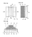
- FIGS. 1A to 1E are a top view and cross-sectional views which illustrate a semiconductor device.
- FIGS. 2A to 2D illustrate a method for manufacturing a semiconductor device.
- FIGS. 3A to 3D illustrate a method for manufacturing a semiconductor device.
- FIGS. 4A to 4C illustrate a method for manufacturing a semiconductor device.
- FIGS. 5A to 5C are a top view and cross-sectional views which illustrate a semiconductor device.
- FIGS. 6A to 6D illustrate a method for manufacturing a semiconductor device.
- FIGS. 7A to 7D are a top view and cross-sectional views which illustrate a semiconductor device.
- FIGS. 8A and 8B illustrate a method for manufacturing a semiconductor device.
- FIGS. 9A to 9C are a top view and cross-sectional views which illustrate a semiconductor device.
- FIGS. 10A to 10C are a top view and cross-sectional views which illustrate a semiconductor device.
- FIG. 11A is a cross-sectional view of a semiconductor device
- FIG. 11B is a circuit diagram thereof.
- FIG. 12A is a circuit diagram of a semiconductor device
- FIG. 12B is a perspective view thereof.
- FIG. 13 is a block diagram of a semiconductor device.
- FIG. 14 is a cross-sectional view of a semiconductor device.
- FIGS. 15A to 15C are block diagrams of a semiconductor device.
- FIGS. 16A to 16C illustrate electronic devices to which a semiconductor device can be applied.
- FIGS. 17A and 17B show results of SIMS analysis of a stacked layer including an IGZO film and a tungsten film.
- FIGS. 18A and 18B show results of SIMS analysis of a stacked layer including an IGZO film and a tantalum nitride film.
- FIGS. 19A and 19B show results of SIMS analysis of a stacked layer including an IGZO film and a titanium nitride film.
- FIGS. 20A and 20B show results of SIMS analysis of a stacked layer including an IGZO film and a tantalum nitride film and a stacked layer including an IGZO film and a titanium nitride film.
- FIGS. 21A and 21B show results of SIMS analysis of a stacked layer including an IGZO film and a tantalum nitride film and a stacked layer including an IGZO film and a titanium nitride film.
- FIG. 22 shows measurement results of sheet resistance values with respect to the depth etching to which an IGZO film is etched.
- FIGS. 23A and 23B show measurement results of sheet resistance values with respect to the depth to which an IGZO film is etched.
- a “source” and a “drain” of a transistor are sometimes replaced with each other when a transistor of opposite polarity is used or when the direction of current flowing is changed in circuit operation, for example.
- the terms “source” and “drain” can be used to denote the drain and the source, respectively, in this specification.
- FIGS. 1A, 1B, 1C, 1D, and 1E are a top view and cross-sectional views which illustrate a transistor of one embodiment of the present invention.
- FIG. 1A is the top view of the transistor, and a cross section taken along a dashed-dotted line X 1 -Y 1 in FIG. 1A is illustrated in FIG. 1B .
- a cross section taken along a dashed-dotted line V 1 -W 1 in FIG. 1A is illustrated in FIG. 1C .
- FIG. 1D illustrates widths of components of the transistor which are illustrated in FIG. 1B .
- FIG. 1E is an enlarged view of a region 105 illustrated in FIG. 1B . Note that for simplification of the drawing, some components in the top view in FIG. 1A are illustrated in a see-through manner or not illustrated.
- a transistor 150 illustrated in FIGS. 1A, 1B, 1C, 1D, and 1E includes an oxide insulating film 104 formed over a substrate 102 ; an oxide semiconductor layer 106 formed over the oxide insulating film 104 ; a first source electrode layer 108 a and a first drain electrode layer 108 b formed over the oxide semiconductor layer 106 ; a second source electrode layer 110 a and a second drain electrode layer 110 b formed over the first source electrode layer 108 a and the first drain electrode layer 108 b , respectively; a gate insulating film 112 formed over the oxide insulating film 104 , the oxide semiconductor layer 106 , the second source electrode layer 110 a , and the second drain electrode layer 110 b ; a gate electrode layer 114 formed over the gate insulating film 112 and in a position overlapping with the oxide semiconductor layer 106 ; and a protective insulating film 116 formed over the gate insulating film 112 and the gate electrode layer 114 .
- another insulating layer another
- the substrate 102 is not limited to a simple supporting substrate, and may be a substrate where another device such as a transistor is formed. In that case, at least one of the gate electrode layer 114 , the first source electrode layer 108 a , the first drain electrode layer 108 b , the second source electrode layer 110 a , and the second drain electrode layer 110 b of the transistor 150 may be electrically connected to the above device.
- the oxide insulating film 104 can have a function of supplying oxygen to the oxide semiconductor layer 106 as well as a function of preventing diffusion of an impurity from the substrate 102 ; thus, the oxide insulating film 104 is an insulating film containing oxygen. It is particularly preferable that the oxide insulating film 104 be an insulating film containing excess oxygen.
- An oxide insulating film containing excess oxygen refers to an oxide insulating film from which oxygen can be released by heat treatment or the like.
- the oxide insulating film containing excess oxygen is preferably a film in which the amount of released oxygen when converted into oxygen atoms is 1.0 ⁇ 10 19 atoms/cm 3 or more in thermal desorption spectroscopy analysis.
- excess oxygen refers to oxygen which can be transferred in the oxide semiconductor layer, silicon oxide, or silicon oxynitride by heat treatment, oxygen in excess of an intrinsic stoichiometric composition, or oxygen which can fill Vo (oxygen vacancy) caused by lack of oxygen.
- Oxygen released from the oxide insulating film 104 can be diffused to a channel formation region of the oxide semiconductor layer 106 , so that oxygen vacancies which might be formed in the oxide semiconductor layer can be filled with the oxygen. In this manner, stable electrical characteristics of the transistor can be achieved.
- oxide insulating film 104 is provided in contact with the oxide semiconductor layer 106 , oxygen can be directly diffused to the oxide semiconductor layer 106 from a lower side of the oxide semiconductor layer 106 . Moreover, since the oxide insulating film 104 is provided in contact with the gate insulating film 112 , oxygen can be diffused to the oxide semiconductor layer 106 from an upper side of the oxide semiconductor layer 106 through the gate insulating film 112 .
- oxygen is introduced into the gate insulating film 112 by an ion implantation method and diffused to the oxide semiconductor layer 106 to the gate insulating film 112 .
- oxygen released from the oxide insulating film 104 can enter the upper side region of the oxide semiconductor layer 106 , which serves as a channel, by being transferred from the outside of the second source electrode layer 110 a (the left side in FIG. 1B ) and the outside of the second drain electrode layer 110 b (the right side in FIG. 1B ) through the gate insulating film 112 .
- the gate insulating film 112 is partly in contact with the oxide insulating film 104 so as to cover the second source electrode layer 110 a and the second drain electrode layer 110 b.
- the gate insulating film 112 is provided between the protective insulating film 116 , and the second source electrode layer 110 a and the second drain electrode layer 110 b so that oxygen released from the oxide insulating film 104 can be diffused to the channel formation region in the oxide semiconductor layer 106 . Accordingly, a material to which little oxygen is diffused or transferred is used for the second source electrode layer 110 a , the second drain electrode layer 110 b , and the protective insulating film 116 . In this manner, when oxygen is diffused to the oxide semiconductor layer through the gate insulating film, diffusion or transfer of oxygen to the source electrode layer and the drain electrode layer can be suppressed.
- excess oxygen can be supplied from the oxide insulating film 104 and the gate insulating film 112 to the channel formation region of the oxide semiconductor layer 106 , whereby the transistor including the oxide semiconductor layer 106 has normally-off characteristics with a positive threshold voltage.
- a semiconductor device in which an increase in oxygen vacancies in the oxide semiconductor layer 106 is suppressed. Further, a highly reliable semiconductor device can be provided.
- the oxide insulating film 104 also has a function as an interlayer insulating film.
- the oxide insulating film 104 is preferably subjected to planarization treatment such as chemical mechanical polishing (CMP) treatment so as to have a flat surface.
- CMP chemical mechanical polishing
- An oxide semiconductor that can be used for the oxide semiconductor layer 106 preferably contains at least indium (In) or zinc (Zn). Alternatively, the oxide semiconductor preferably contains both In and Zn. Details of a material and a formation method which can be used for the oxide semiconductor layer 106 are to be described in description of a method for manufacturing the transistor.
- substantially intrinsic refers to the state where an oxide semiconductor layer has a carrier density lower than 1 ⁇ 10 17 /cm 3 , preferably lower than 1 ⁇ 10 15 /cm 3 , further preferably lower than 1 ⁇ 10 13 /cm 3 .
- hydrogen, nitrogen, carbon, silicon, and metal elements except main components of the oxide semiconductor are impurities.
- hydrogen and nitrogen form donor levels to increase the carrier density.
- Silicon forms impurity levels in an oxide semiconductor layer. The impurity levels serve as traps and might cause electrical characteristics of the transistor to deteriorate.
- An oxide semiconductor layer can be intrinsic or substantially intrinsic under the following conditions: in SIMS analysis, the concentration of silicon is lower than 1 ⁇ 10 19 atoms/cm 3 , preferably lower than 5 ⁇ 10 18 atoms/cm 3 , further preferably lower than 1 ⁇ 10 18 atoms/cm 3 ; the concentration of hydrogen is lower than or equal to 2 ⁇ 10 20 atoms/cm 3 , preferably lower than or equal to 5 ⁇ 10 19 atoms/cm 3 , further preferably lower than or equal to 1 ⁇ 10 19 atoms/cm 3 , still further preferably lower than or equal to 5 ⁇ 10 18 atoms/cm 3 ; and the concentration of nitrogen is lower than 5 ⁇ 10 19 atoms/cm 3 , preferably lower than or equal to 5 ⁇ 10 18 atoms/cm 3 , further preferably lower than or equal to 1 ⁇ 10 18 atoms/cm 3 , still further preferably lower than or equal to 5 ⁇ 10 17 atoms/cm 3 .
- the oxide semiconductor layer includes crystals
- high concentration of silicon or carbon might reduce the crystallinity of the oxide semiconductor layer.
- the crystallinity of the oxide semiconductor layer can be prevented from decreasing when the concentration of silicon is lower than 1 ⁇ 10 19 atoms/cm 3 , preferably lower than 5 ⁇ 10 18 atoms/cm 3 , further preferably lower than 1 ⁇ 10 18 atoms/cm 3
- the concentration of carbon is lower than 1 ⁇ 10 19 atoms/cm 3 , preferably lower than 5 ⁇ 10 18 atoms/cm 3 , further preferably lower than 1 ⁇ 10 18 atoms/cm 3 .
- a transistor in which a highly purified oxide semiconductor film is used for a channel formation region as described above has extremely low off-state current, and the off-state current standardized on the channel width of the transistor can be as low as several yoktoamperes per micrometer to several zeptoamperes per micrometer.
- the absorption coefficient due to the localized states in the oxide semiconductor layer 106 which is obtained in measurement by a constant photocurrent method (CPM), is set lower than 1 ⁇ 10 ⁇ 3 /cm, preferably lower than 3 ⁇ 10 ⁇ 4 /cm.
- a conductive material which is easily bonded to oxygen can be used.
- Al, Cr, Cu, Ta, Ti, Mo, or W can be used.
- W with a high melting point is preferably used, which allows subsequent process temperatures to be relatively high.
- the conductive material which is easily bonded to oxygen includes, in its category, a material to which oxygen is easily diffused or transferred.
- the conductive material which is easily bonded to oxygen When the conductive material which is easily bonded to oxygen is in contact with an oxide semiconductor layer, a phenomenon occurs in which oxygen of the oxide semiconductor layer is diffused or transferred to the conductive material which is easily bonded to oxygen. Since the manufacturing process of the transistor involves some heat treatment steps, the above phenomenon causes generation of oxygen vacancies in a region of the oxide semiconductor layer, which is in contact with the source electrode or the drain electrode, and the region becomes an n-type. Thus, the n-type region can serve as a source or a drain of the transistor.
- the n-type region which is formed by the generation of the oxygen vacancies sometimes extends in the channel length direction of the transistor.
- electrical characteristics of the transistor change; for example, the threshold voltage is shifted or on and off of the transistor cannot be controlled with the gate voltage (i.e., the transistor is on). Accordingly, when a transistor with an extremely short channel length is formed, it is not preferable that the conductive material which is easily bonded to oxygen be used for a source electrode and a drain electrode.
- the source electrode and the drain electrode have stacked-layer structures, and the second source electrode layer 110 a and the second drain electrode layer 110 b , which determine the channel length, are formed using the conductive material which is not easily bonded to oxygen.
- the conductive material for example, a conductive nitride such as tantalum nitride or titanium nitride, or ruthenium is preferably used.
- the conductive material which is not easily bonded to oxygen includes, in its category, a material to which oxygen is not easily diffused or transferred.
- the channel length refers to a distance between the second source electrode layer 110 a and the second drain electrode layer 110 b.
- the contact resistance with the oxide semiconductor layer 106 becomes too high; thus, it is preferable that as illustrated in FIG. 1B , the first source electrode layer 108 a and the first drain electrode layer 108 b be formed over the oxide semiconductor layer 106 and the second source electrode layer 110 a and the second drain electrode layer 110 b be formed so as to cover the first source electrode layer 108 a and the first drain electrode layer 108 b.
- the oxide semiconductor layer 106 have a large contact area with the first source electrode layer 108 a or the first drain electrode layer 108 b , and the oxide semiconductor layer 106 have a small contact area with the second source electrode layer 110 a or the second drain electrode layer 110 b .
- the region of the oxide semiconductor layer 106 which is in contact with the first source electrode layer 108 a or the first drain electrode layer 108 b , becomes an n-type region due to generation of oxygen vacancies. Owing to the n-type region, the contact resistance between the oxide semiconductor layer 106 and the first source electrode layer 108 a or the first drain electrode layer 108 b can be reduced. Accordingly, when the oxide semiconductor layer 106 has a large contact area with the first source electrode layer 108 a or the first drain electrode layer 108 b , the area of the n-type region can also be large.
- FIG. 1E is an enlarged view of a region 105 illustrated in FIG. 1B , and in the region of the oxide semiconductor layer 106 , which is in contact with the first source electrode layer 108 a , oxygen of the oxide semiconductor layer 106 is extracted to the first source electrode layer 108 a side, so that an n-type region 106 a is formed.
- the n-type region 106 a is a region of the oxide semiconductor layer 106 , which includes many oxygen vacancies.
- a component of the first source electrode layer 108 a for example, a tungsten element in the case where a tungsten film is used for the first source electrode layer 108 a , enters the n-type region 106 a .
- a mixed layer might be formed due to entry of oxygen of the oxide semiconductor layer 106 into a region of the first source electrode layer 108 a , which is in contact with the oxide semiconductor layer 106 .
- region 105 has been described with reference to the enlarged view illustrating the oxide semiconductor layer 106 and the first source electrode layer 108 a , the above-described n-type region is also formed on the first drain electrode layer 108 b side of the oxide semiconductor layer 106 .
- n-type region 106 a may be used as a source region or a drain region in the oxide semiconductor layer 106 .
- the conductive material which is not easily bonded to oxygen is used for the second source electrode layer 110 a and the second drain electrode layer 110 b .
- the oxide semiconductor layer 106 is supplied with oxygen of the oxide insulating film 104 from the upper side of the oxide semiconductor layer 106 through the gate insulating film 112 , the oxygen is less likely to be diffused or transferred to the second source electrode layer 110 a and the second drain electrode layer 110 b . Accordingly, oxygen can be favorably supplied to the oxide semiconductor layer 106 .
- the gate insulating film 112 can be formed using an insulating film containing one or more of aluminum oxide, magnesium oxide, silicon oxide, silicon oxynitride, silicon nitride oxide, silicon nitride, gallium oxide, germanium oxide, yttrium oxide, zirconium oxide, lanthanum oxide, neodymium oxide, hafnium oxide, and tantalum oxide.
- the gate insulating film 112 may be a stack of any of the above materials.
- a conductive film including a material such as Al, Ti, Cr, Co, Ni, Cu, Y, Zr, Mo, Ru, Ag, Ta, or W can be used. Further, the gate electrode layer 114 may be a stack of any of the above materials.
- a material to which little oxygen is diffused or transferred be used for the protective insulating film 116 .
- a material containing little hydrogen when formed into a film is preferably used for the protective insulating film 116 .
- the hydrogen content of the protective insulating film 116 is preferably lower than 5 ⁇ 10 19 /cm 3 , further preferably lower than 5 ⁇ 10 18 /cm 3 .
- off-state current of the transistor can be low.
- a silicon nitride film or a silicon nitride oxide film is preferably used as the protective insulating film 116 .
- the distance (L 1 ) between the first source electrode layer 108 a and the first drain electrode layer 108 b is set to 0.8 ⁇ m or longer, preferably 1.0 ⁇ m or longer. In the case where L 1 is shorter than 0.8 ⁇ m, influence of oxygen vacancies generated in the channel formation region cannot be eliminated, which might cause deterioration of the electrical characteristics of the transistor.
- the transistor can have favorable electrical characteristics.
- L 0 when the width of the gate electrode layer 114 is referred to as L 0 , L 0 ⁇ L 1 ⁇ L 2 (L 1 is longer than or equal to L 2 and shorter than or equal to L 0 ) is satisfied as illustrated in FIG. 1D so that regions can be formed in which the gate electrode layer 114 overlaps with the source and drain electrode layers (the first source electrode layer 108 a , the second source electrode layer 110 a , the first drain electrode layer 108 b , and the second drain electrode layer 110 b ) with the gate insulating film 112 provided therebetween.
- on-state characteristics e.g., on-state current and field-effect mobility
- L 3 is preferably shorter than 1 ⁇ m and L 4 is preferably longer than or equal to 1 ⁇ m and shorter than or equal to 2.5 ⁇ m.
- L 4 has the respective values, the transistor can be miniaturized.
- the above is the transistor of one embodiment of the present invention, whose structure can suppress an increase in oxygen vacancies in the oxide semiconductor layer. Specifically, in the transistor, oxygen can be supplied from the oxide insulating film and the gate insulating film, which are in contact with the oxide semiconductor layer, to the oxide semiconductor layer. It is thus possible to provide a semiconductor device having favorable electrical characteristics and high long-term reliability.
- a glass substrate, a ceramic substrate, a quartz substrate, a sapphire substrate, or the like can be used.
- a single crystal semiconductor substrate or a polycrystalline semiconductor substrate made of silicon, silicon carbide, or the like, a compound semiconductor substrate made of silicon germanium or the like, a silicon-on-insulator (SOI) substrate, or the like may be used.
- SOI silicon-on-insulator
- the oxide insulating film 104 can be formed by a plasma chemical vapor deposition (CVD) method, a sputtering method, or the like using an oxide insulating film of aluminum oxide, magnesium oxide, silicon oxide, silicon oxynitride, silicon nitride oxide, gallium oxide, germanium oxide, yttrium oxide, zirconium oxide, lanthanum oxide, neodymium oxide, hafnium oxide, tantalum oxide, or the like or a mixed material of any of these.
- CVD plasma chemical vapor deposition
- sputtering method or the like using an oxide insulating film of aluminum oxide, magnesium oxide, silicon oxide, silicon oxynitride, silicon nitride oxide, gallium oxide, germanium oxide, yttrium oxide, zirconium oxide, lanthanum oxide, neodymium oxide, hafnium oxide, tantalum oxide, or the like or a mixed material of any of these.
- a stack of any of the above materials may be used, and at least an upper layer of the oxide insulating film 104 , which is in contact with the oxide semiconductor layer 106 , is formed using a material containing oxygen which might serve as a supply source of oxygen to the oxide semiconductor layer 106 .
- Oxygen may be added to the oxide insulating film 104 by an ion implantation method, an ion doping method, a plasma immersion ion implantation method, or the like. By addition of oxygen, the oxide insulating film 104 can further contain excess oxygen.
- an oxide semiconductor layer is formed over the oxide insulating film 104 by a sputtering method, a CVD method, a molecular beam epitaxy (MBE) method, an atomic layer deposition (ALD) method, or a pulse laser deposition (PLD) method and selectively etched, so that the oxide semiconductor layer 106 is formed (see FIG. 2A ). Note that heating may be performed before etching.
- An oxide semiconductor that can be used for the oxide semiconductor layer 106 preferably contains at least indium (In) or zinc (Zn).
- the oxide semiconductor preferably contains both In and Zn.
- the oxide semiconductor preferably contains a stabilizer in addition to In and Zn.
- gallium (Ga), tin (Sn), hafnium (Hf), aluminum (Al), zirconium (Zr), and the like can be given.
- lanthanoid such as lanthanum (La), cerium (Ce), praseodymium (Pr), neodymium (Nd), samarium (Sm), europium (Eu), gadolinium (Gd), terbium (Tb), dysprosium (Dy), holmium (Ho), erbium (Er), thulium (Tm), ytterbium (Yb), or lutetium (Lu) can be given.
- an In—Ga—Zn oxide refers to, for example, an oxide containing In, Ga, and Zn as its main components and there is no particular limitation on the ratio of In to Ga and Zn.
- the In—Ga—Zn oxide may contain a metal element other than In, Ga, and Zn.
- a film formed using an In—Ga—Zn oxide is also referred to as an IGZO film.
- a material represented by InMO 3 (ZnO) m (m>0, where m is not an integer) may be used.
- M represents one or more metal elements selected from Ga, Fe, Mn, and Co.
- a material represented by In 2 SnO 5 (ZnO) n (n>0, where n is an integer) may be used.
- the oxide semiconductor film is preferably formed by a sputtering method.
- a sputtering method an RF sputtering method, a DC sputtering method, an AC sputtering method, or the like can be used.
- a DC sputtering method is preferably used because dust generated in the deposition can be reduced and the film thickness can be uniform.
- the oxide semiconductor film a film in a single crystal state, a polycrystalline (also referred to as polycrystal) state, an amorphous state, or the like can be used.
- the oxide semiconductor film is preferably a c-axis aligned crystalline oxide semiconductor (CAAC-OS) film.
- Sputtering may be performed to form an oxide semiconductor film including a CAAC-OS film.
- a CAAC-OS film by sputtering it is important to form crystals in a hexagonal configuration in an initial stage of deposition of an oxide semiconductor film and to cause crystal growth from the crystals as cores.
- the distance between the target and the substrate be made to be longer (e.g., 150 mm to 200 mm) and a substrate heating temperature be 100° C. to 500° C., more preferably 200° C. to 400° C., still preferably 250° C. to 300° C.
- the deposited oxide semiconductor film is subjected to heat treatment at a temperature higher than the substrate heating temperature in the deposition. Therefore, micro-defects in the film and defects at the interface of a stacked layer can be compensated.
- the CAAC-OS film is one of oxide semiconductor films having a plurality of c-axis aligned crystal parts.
- TEM transmission electron microscope
- a boundary between crystal parts, that is, a grain boundary is not clearly observed.
- metal atoms are arranged in a layered manner in the crystal parts.
- Each metal atom layer has a morphology reflected by a surface over which the CAAC-OS film is formed (hereinafter, a surface over which the CAAC-OS film is formed is referred to as a formation surface) or a top surface of the CAAC-OS film, and is arranged in parallel to the formation surface or the top surface of the CAAC-OS film.
- a surface over which the CAAC-OS film is formed is referred to as a formation surface
- a top surface of the CAAC-OS film is arranged in parallel to the formation surface or the top surface of the CAAC-OS film.
- metal atoms are arranged in a triangular or hexagonal configuration in the crystal parts. However, there is no regularity of arrangement of metal atoms between different crystal parts.
- a c-axis is aligned in a direction parallel to a normal vector of a surface where the CAAC-OS film is formed or a normal vector of a surface of the CAAC-OS film, triangular or hexagonal atomic arrangement which is seen from the direction perpendicular to the a-b plane is formed, and metal atoms are arranged in a layered manner or metal atoms and oxygen atoms are arranged in a layered manner when seen from the direction perpendicular to the c-axis.
- the directions of the a-axis and the b-axis of one crystal part may be different from those of another crystal part.
- a simple term “perpendicular” includes a range from 85° to 95°.
- a simple term “parallel” includes a range from ⁇ 5° to 5°.
- the proportion of the c-axis aligned crystal parts in the vicinity of the top surface is higher than that in the vicinity of the formation surface in some cases.
- an impurity is added to the CAAC-OS film, a region to which the impurity is added is altered, and the proportion of the c-axis aligned crystal parts in the CAAC-OS film varies depending on regions, in some cases.
- the directions of the c-axes may be different from each other depending on the shape of the CAAC-OS film (the cross-sectional shape of the surface where the CAAC-OS film is formed or the cross-sectional shape of the surface of the CAAC-OS film). Note that when the CAAC-OS film is formed, the direction of c-axis of the crystal part is the direction parallel to a normal vector of the surface where the CAAC-OS film is formed or a normal vector of the surface of the CAAC-OS film.
- the crystal part is formed by film formation or by performing treatment for crystallization such as heat treatment after film formation.
- the transistor With use of the CAAC-OS film in a transistor, change in electric characteristics of the transistor due to irradiation with visible light or ultraviolet light is small. Thus, the transistor has high reliability.
- a CAAC-OS film can be deposited by a sputtering method using a polycrystalline oxide semiconductor sputtering target.
- a crystal region included in the sputtering target might be separated from the target along an a-b plane; in other words, a sputtered particle having a plane parallel to an a-b plane (flat-plate-like sputtered particle or pellet-like sputtered particle) might be separated from the sputtering target.
- the flat-plate-like sputtered particle reaches a substrate while maintaining their crystal state, whereby the CAAC-OS film can be formed.
- the following conditions are preferably used.
- the crystal state can be prevented from being distorted by the impurities.
- impurities e.g., hydrogen, water, carbon dioxide, or nitrogen
- impurities in a deposition gas may be reduced.
- a deposition gas whose dew point is ⁇ 80° C. or lower, preferably ⁇ 100° C. or lower is used.
- the substrate heating temperature during the deposition is higher than or equal to 100° C. and lower than or equal to 740° C., preferably higher than or equal to 200° C. and lower than or equal to 500° C.
- the proportion of oxygen in the deposition gas be increased and the power be optimized in order to reduce plasma damage at the deposition.
- the proportion of oxygen in the deposition gas is 30 vol % or higher, preferably 100 vol %.
- an In—Ga—Zn—O compound target is described below.
- the In—Ga—Zn—O compound target which is polycrystalline, is made by mixing InO X powder, GaO Y powder, and ZnO Z powder in a predetermined molar ratio, applying pressure, and performing heat treatment at a temperature higher than or equal to 1000° C. and lower than or equal to 1500° C.
- X, Y, and Z are each a given positive number.
- the kinds of powder and the molar ratio for mixing powder may be determined as appropriate depending on the sputtering target that is formed.
- first heat treatment is preferably performed.
- the first heat treatment may be performed at a temperature higher than or equal to 250° C. and lower than or equal to 650° C., preferably higher than or equal to 300° C. and lower than or equal to 500° C., in an inert gas atmosphere, an atmosphere containing an oxidizing gas at 10 ppm or more, or a reduced pressure state.
- the first heat treatment may be performed in such a manner that heat treatment is performed in an inert gas atmosphere, and then another heat treatment is performed in an atmosphere containing an oxidizing gas at 10 ppm or more in order to compensate released oxygen.
- the crystallinity of the oxide semiconductor layer 106 can be improved, and in addition, impurities such as hydrogen and water can be removed from the oxide insulating film 104 and the oxide semiconductor layer 106 .
- the step of the first heat treatment may be performed before etching for formation of the oxide semiconductor layer 106 .
- a first conductive film 108 to be the first source electrode layer 108 a and the first drain electrode layer 108 b is formed over the oxide semiconductor layer 106 (see FIG. 2B ).
- Al, Cr, Cu, Ta, Ti, Mo, W, or an alloy material containing any of these as a main component can be used.
- a 100-nm-thick tungsten film is formed by a sputtering method or the like.
- resist masks 190 a and 190 b are formed over the first conductive film 108 (see FIG. 2C ).
- the first conductive film 108 is etched so as to be divided over the oxide semiconductor layer 106 with use of the resist masks 190 a and 190 b as masks, so that the first source electrode layer 108 a and the first drain electrode layer 108 b are formed; then, the resist masks 190 a and 190 b are removed (see FIG. 2D ).
- the first conductive film 108 is over-etched, so that the oxide semiconductor layer 106 is partly etched as illustrated in FIG. 2D .
- the oxide semiconductor layer 106 is hardly etched.
- the oxide insulating film 104 on outer sides than the edges of the first source electrode layer 108 a and the first drain electrode layer 108 b is etched as illustrated in FIG. 2D .
- a second conductive film 110 that is to be the second source electrode layer 110 a and the second drain electrode layer 110 b is formed over the oxide semiconductor layer 106 , the first source electrode layer 108 a , and the first drain electrode layer 108 b (see FIG. 3A ).
- a conductive nitride such as tantalum nitride or titanium nitride, ruthenium, or an alloy material containing any of these as a main component can be used.
- a 20-nm-thick tantalum nitride film is formed by a sputtering method or the like.
- the second conductive film 110 is etched so as to be divided, so that the second source electrode layer 110 a and the second drain electrode layer 110 b are formed (see FIG. 3B ).
- part of the oxide semiconductor layer 106 may be etched.
- part of the oxide insulating film 104 at the time of etching for formation of the second source electrode layer 110 a and the second drain electrode layer 110 b , part of the oxide insulating film 104 , more specifically, the oxide insulating film 104 on outer sides than the edges of the second source electrode layer 110 a and the second drain electrode layer 110 b may be etched.
- the second source electrode layer 110 a and the second drain electrode layer 110 b can be formed in such a manner that the second conductive film 110 is etched first so as to cover the first source electrode layer 108 a and the first drain electrode layer 108 b , and then etched using resist masks that are processed by a method suitable for fine line processing, such as electron beam exposure. Note that by use of a positive type resist for the resist masks, the exposed region can be minimized and throughput can be thus improved. In the above manner, a transistor having a channel length of 30 nm or less can be formed.
- second heat treatment is preferably performed.
- the second heat treatment can be performed under a condition similar to that of the first heat treatment.
- impurities such as hydrogen and water can be further removed from the oxide semiconductor layer 106 .
- the gate insulating film 112 is formed over the oxide insulating film 104 , the oxide semiconductor layer 106 , the second source electrode layer 110 a , and the second drain electrode layer 110 b .
- the gate insulating film 112 can be formed using aluminum oxide, magnesium oxide, silicon oxide, silicon oxynitride, silicon nitride oxide, silicon nitride, gallium oxide, germanium oxide, yttrium oxide, zirconium oxide, lanthanum oxide, neodymium oxide, hafnium oxide, tantalum oxide, or the like.
- the gate insulating film 112 may be a stack of any of the above materials.
- the gate insulating film 112 can be formed by a sputtering method, a CVD method, an MBE method, an ALD method, a PLD method, or the like.
- the gate insulating film 112 be successively subjected to heat treatment after being formed.
- the gate insulating film 112 is formed with a PE-CVD apparatus and is successively subjected to heat treatment in a vacuum.
- the heat treatment can remove hydrogen, moisture, and the like from the gate insulating film 112 .
- the gate insulating film 112 can be dehydrated or dehydrogenated to be dense.
- FIG. 3C is a schematic view which illustrates addition of oxygen 120 into the gate insulating film 112 .
- the oxygen 120 contains at least any of an oxygen radical, ozone, an oxygen atom, and an oxygen ion (including an oxygen molecular ion or an oxygen cluster ion).
- the step of adding oxygen into the gate insulating film 112 may be performed after formation of a gate electrode or after formation of a protective insulating film.
- a third conductive film 113 that is to be the gate electrode layer 114 is formed over the gate insulating film 112 , and then a resist mask 192 is formed in a desired region (see FIG. 3D ).
- a resist mask 192 is formed in a desired region (see FIG. 3D ).
- Al, Ti, Cr, Co, Ni, Cu, Y, Zr, Mo, Ru, Ag, Ta, W, or an alloy material containing any of these as a main component can be used.
- the third conductive film 113 can be formed by a sputtering method.
- the third conductive film 113 is etched, so that the gate electrode layer 114 is formed; then, the resist mask 192 is removed (see FIG. 4A ).
- the protective insulating film 116 is formed over the gate insulating film 112 and the gate electrode layer 114 . It is preferable that a material to which little oxygen is diffused or transferred be used for the protective insulating film 116 . Further, a material containing little hydrogen when formed into a film is preferably used for the protective insulating film 116 .
- the hydrogen content of the protective insulating film 116 is preferably lower than 5 ⁇ 10 19 /cm 3 , further preferably lower than 5 ⁇ 10 18 /cm 3 . When the hydrogen content of the protective insulating film 116 has the above value, off-state current of the transistor can be low.
- a silicon nitride film or a silicon nitride oxide film is preferably used as the protective insulating film 116 .
- the protective insulating film 116 can be formed by a sputtering method, a CVD method, an MBE method, an ALD method, or a PLD method.
- a silicon nitride film is preferably formed by a sputtering method, in which case the content of water or hydrogen is low.
- the oxygen 120 is added to the gate insulating film 112 by an ion implantation method, an ion doping method, a plasma immersion ion implantation method, or the like (see FIG. 4B ). Addition of the oxygen in this step is performed through the protective insulating film 116 . Further, the number of times of the step of adding oxygen is not particularly limited as long as the step is performed after formation of the gate insulating film 112 , and the step may be performed after formation of the gate electrode layer 114 , and further performed after formation of the protective insulating film 116 .
- addition of oxygen is not necessarily performed twice (one is performed after the formation of the gate insulating film 112 and the other is performed after formation of the protective insulating film 116 ), and either one of the steps may be performed.
- Oxygen may be added to the entire surface of the substrate at a time.
- a linear ion beam may be used, for example.
- the substrate or the ion beam is relatively moved (scanned), whereby the oxygen 120 can be introduced into the entire area of the gate insulating film 112 .
- a gas containing oxygen (O) can be used; for example, an O 2 gas, an N 2 O gas, a CO 2 gas, a CO gas, or an NO 2 gas can be used.
- a rare gas e.g., an Ar gas
- a rare gas may be contained in the supply gas of the oxygen.
- the dose of the oxygen 120 is preferably greater than or equal to 1 ⁇ 10 13 ions/cm 2 and less than or equal to 5 ⁇ 10 16 ions/cm 2 .
- the dose of the oxygen 120 is preferably greater than or equal to 1 ⁇ 10 13 ions/cm 2 and less than or equal to 5 ⁇ 10 16 ions/cm 2 .
- x in the insulating film containing excess oxygen is preferably greater than 2. Note that such a region containing oxygen in excess of the stoichiometric composition may exist in part of the gate insulating film 112 .
- the depth at which oxygen is introduced may be adjusted as appropriate by implantation conditions.
- third heat treatment is preferably performed.
- the third heat treatment can be performed under a condition similar to that of the first heat treatment.
- oxygen is easily released from the oxide insulating film 104 and the gate insulating film 112 , so that oxygen vacancies in the oxide semiconductor layer 106 can be reduced.
- the transistor 150 illustrated in FIGS. 1A to 1E and FIG. 4C can be manufactured.
- FIGS. 5A, 5B, and 5C are a top view and cross-sectional views which illustrate a transistor of one embodiment of the present invention.
- FIG. 5A is the top view of the transistor, and a cross section taken along a dashed-dotted line X 2 -Y 2 in FIG. 5A is illustrated in FIG. 5B .
- a cross section taken along a dashed-dotted line V 2 -W 2 in FIG. 5A is illustrated in FIG. 5C .
- some components in the top view in FIG. 5A are illustrated in a see-through manner or not illustrated. Note that the same portions as or portions having functions similar to those of the transistor described in Embodiment 1 are denoted by the same reference numerals, and repeated description thereof is omitted.
- a transistor 152 illustrated in FIGS. 5A, 5B, and 5C includes the oxide insulating film 104 formed over the substrate 102 ; the oxide semiconductor layer 106 formed over the oxide insulating film 104 ; a first source electrode layer 168 a and a first drain electrode layer 168 b formed over the oxide semiconductor layer 106 ; the second source electrode layer 110 a and the second drain electrode layer 110 b formed over the first source electrode layer 168 a and the first drain electrode layer 168 b , respectively; the gate insulating film 112 formed over the oxide insulating film 104 , the oxide semiconductor layer 106 , the second source electrode layer 110 a , and the second drain electrode layer 110 b ; the gate electrode layer 114 formed over the gate insulating film 112 and in a position overlapping with the oxide semiconductor layer 106 ; and the protective insulating film 116 formed over the gate insulating film 112 and the gate electrode layer 114 .
- another insulating layer, another wiring, or the like may be formed over the
- the transistor 152 described in this embodiment is different from the transistor 150 described in Embodiment 1 in the shapes of the first source electrode layer 168 a and the first drain electrode layer 168 b .
- the second source electrode layer 110 a , the second drain electrode layer 110 b , the gate insulating film 112 , the gate electrode layer 114 , and the protective insulating film 116 which are formed over the first source electrode layer 168 a and the first drain electrode layer 168 b have shapes corresponding to the shapes of the first source electrode layer 168 a and the first drain electrode layer 168 b.
- the second source electrode layer 110 a , the second drain electrode layer 110 b , and the gate insulating film 112 can have favorable coverage.
- oxygen released from the oxide insulating film 104 is likely to be diffused to an upper region of the oxide semiconductor layer 106 , which serves as a channel, through the gate insulating film 112 .
- steps before FIG. 6A are performed in a manner similar to those up to FIG. 2C in the manufacturing process of the transistor 150 (see FIG. 6A ). Note that the cross-sectional structure illustrated in FIG. 6A is the same as that illustrated in FIG. 2C .
- the first conductive film 108 is etched using the resist masks 190 a and 190 b to form the first source electrode layer 108 a and the first drain electrode layer 108 b (see FIG. 6B ).
- resist masks 194 a and 194 b are formed by making the resist masks 190 a and 190 b recede or reducing them by ashing (see FIG. 6C ).
- the first source electrode layer 108 a and the first drain electrode layer 108 b are etched using the resist masks 194 a and 194 b and then the resist masks 194 a and 194 b are removed, whereby the first source electrode layer 168 a and the first drain electrode layer 168 b are formed (see FIG. 6D ).
- the end portions of the first source electrode layer 168 a and the first drain electrode layer 168 b can have staircase-like shapes.
- the above is the transistor of one embodiment of the present invention, whose structure can suppress an increase in oxygen vacancies in the oxide semiconductor layer. Specifically, in the transistor, oxygen can be supplied from the oxide insulating film and the gate insulating film which are in contact with the oxide semiconductor layer to the oxide semiconductor layer. It is thus possible to provide a semiconductor device having favorable electrical characteristics and high long-term reliability.
- FIGS. 7A, 7B, 7C, and 7D are a top view and cross-sectional views which illustrate a transistor of one embodiment of the present invention.
- FIG. 7A is the top view of the transistor, and a cross section taken along a dashed-dotted line X 3 -Y 3 in FIG. 7A is illustrated in FIG. 7B .
- a cross section taken along a dashed-dotted line V 3 -W 3 in FIG. 7A is illustrated in FIG. 7C .
- FIG. 7D illustrates widths of components of the transistor which are illustrated in FIG. 7B . Note that for simplification of the drawing, some components in the top view in FIG. 7A are illustrated in a see-through manner or not illustrated. Note that the same portions as or portions having functions similar to those of the transistor described in Embodiment 1 are denoted by the same reference numerals, and repeated description thereof is omitted.
- a transistor 154 illustrated in FIGS. 7A, 7B, 7C, and 7D includes the oxide insulating film 104 formed over the substrate 102 ; the oxide semiconductor layer 106 formed over the oxide insulating film 104 ; the first source electrode layer 108 a and the first drain electrode layer 108 b formed over the oxide semiconductor layer 106 ; the second source electrode layer 110 a and the second drain electrode layer 110 b formed over the first source electrode layer 108 a and the first drain electrode layer 108 b , respectively; the gate insulating film 112 formed over the oxide insulating film 104 , the oxide semiconductor layer 106 , the second source electrode layer 110 a , and the second drain electrode layer 110 b ; a gate electrode layer 174 formed over the gate insulating film 112 and in a position overlapping with the oxide semiconductor layer 106 ; and the protective insulating film 116 formed over the gate insulating film 112 and the gate electrode layer 174 .
- another insulating layer, another wiring, or the like may be formed
- the transistor 154 described in this embodiment is different from the transistor 150 described in Embodiment 1 in the shape of the gate electrode layer 174 .
- the gate electrode layer 114 is provided in a position overlapping with the first source electrode layer 108 a , the first drain electrode layer 108 b , the second source electrode layer 110 a , and the second drain electrode layer 110 b ; however, in the transistor 154 described in this embodiment, the gate electrode layer 174 is provided in a position overlapping with the second source electrode layer 110 a and the second drain electrode layer 110 b . In other words, the gate electrode layer 174 is not provided in a position overlapping with the first source electrode layer 108 a and the first drain electrode layer 108 b.
- the distance (L 1 ) between the first source electrode layer 108 a and the first drain electrode layer 108 b is set to 0.8 ⁇ m or longer, preferably 1.0 ⁇ m or longer. In the case where L 1 is shorter than 0.8 ⁇ m, influence of oxygen vacancies generated in the channel formation region cannot be eliminated, which might cause deterioration of the electrical characteristics of the transistor.
- the transistor can have favorable electrical characteristics.
- L 0 When the width of the gate electrode layer 174 is referred to as L 0 , L 1 ⁇ L 0 ⁇ L 2 (L 0 is longer than or equal to L 2 and shorter than or equal to L 1 ) is satisfied so that parasitic capacitance which is caused between the gate and the drain and between the gate and the source can be made small as much as possible. Accordingly, the frequency characteristics of the transistor can be improved. Note that in order to obtain favorable electrical characteristics of the transistor, it is preferable that a difference between L 0 and L 2 be greater than or equal to 2 nm and less than or equal to 20 nm and a difference between L 1 and L 2 be greater than or equal to 20 nm and less than or equal to 1 ⁇ m.
- L 0 ⁇ L 1 ⁇ L 2 (L 1 is longer than or equal to L 2 and shorter than or equal to L 0 ) may be satisfied as illustrated in FIG. 1B .
- L 1 is longer than or equal to L 2 and shorter than or equal to L 0
- the degree of difficulty in formation steps of the gate electrode can be lowered.
- L 3 is preferably shorter than 1 ⁇ m and L 4 is preferably longer than or equal to 1 ⁇ m and shorter than or equal to 2.5 ⁇ m.
- L 4 has the respective values, the transistor can be miniaturized.
- steps before FIG. 8A are performed in a manner similar to those up to FIG. 3D in the manufacturing process of the transistor 150 (see FIG. 8A ). Note that the cross section illustrated in FIG. 8A is different from the cross section illustrated in FIG. 3D in the shape of a resist mask 196 .
- the resist mask 196 a mask having a finer pattern which is formed by performing a slimming process on a mask formed by a photolithography method or the like is preferably used.
- an ashing process in which oxygen in a radical state (an oxygen radical) is used can be employed, for example.
- the line width of the mask formed by a photolithography method or the like can be reduced to a length shorter than or equal to the resolution limit of a light exposure apparatus, preferably less than or equal to half of the resolution limit of a light exposure apparatus, further preferably less than or equal to one third of the resolution limit of the light exposure apparatus.
- the line width can be greater than or equal to 20 nm and less than or equal to 2000 nm, preferably greater than or equal to 50 nm and less than or equal to 350 nm.
- the third conductive film 113 is etched with use of the resist mask 196 , so that the gate electrode layer 174 is formed (see FIG. 8B ).
- the above is the transistor of one embodiment of the present invention, whose structure can suppress an increase in oxygen vacancies in the oxide semiconductor layer. Specifically, in the transistor, oxygen can be supplied from the oxide insulating film and the gate insulating film which are in contact with the oxide semiconductor layer to the oxide semiconductor layer. It is thus possible to provide a semiconductor device having favorable electrical characteristics and high long-term reliability.
- FIGS. 9A, 9B, and 9C are a top view and cross-sectional views which illustrate a transistor of one embodiment of the present invention.
- FIG. 9A is the top view of the transistor, and a cross section taken along a dashed-dotted line X 4 -Y 4 in FIG. 9A is illustrated in FIG. 9B .
- a cross section taken along a dashed-dotted line V 4 -W 4 in FIG. 9A is illustrated in FIG. 9C .
- some components in the top view in FIG. 9A are illustrated in a see-through manner or not illustrated. Note that the same portions as or portions having functions similar to those of the transistor described in Embodiment 1 are denoted by the same reference numerals, and repeated description thereof is omitted.
- the transistor 156 illustrated in FIGS. 9A, 9B, and 9C includes the oxide insulating film 104 formed over the substrate 102 ; the oxide semiconductor layer 106 formed over the oxide insulating film 104 ; the first source electrode layer 168 a and the first drain electrode layer 168 b formed over the oxide semiconductor layer 106 ; the second source electrode layer 110 a and the second drain electrode layer 110 b formed over the first source electrode layer 168 a and the first drain electrode layer 168 b , respectively; the gate insulating film 112 formed over the oxide insulating film 104 , the oxide semiconductor layer 106 , the second source electrode layer 110 a , and the second drain electrode layer 110 b ; the gate electrode layer 174 formed over the gate insulating film 112 and in a position overlapping with the oxide semiconductor layer 106 ; and the protective insulating film 116 formed over the gate insulating film 112 and the gate electrode layer 174 .
- another insulating layer, another wiring, or the like may be formed over the protective
- the transistor 156 described in this embodiment is different from the transistor 150 described in Embodiment 1 in the shapes of the first source electrode layer 168 a , the first drain electrode layer 168 b , and the gate electrode layer 174 .
- the second source electrode layer 110 a , the second drain electrode layer 110 b , the gate insulating film 112 , the gate electrode layer 174 , and the protective insulating film 116 which are formed over the first source electrode layer 168 a and the first drain electrode layer 168 b have shapes corresponding to the shapes of the first source electrode layer 168 a and the first drain electrode layer 168 b.
- the gate electrode layer 114 is provided in a position overlapping with the first source electrode layer 108 a , the first drain electrode layer 108 b , the second source electrode layer 110 a , and the second drain electrode layer 110 b ; however, in the transistor 156 described in this embodiment, the gate electrode layer 174 is provided in a position overlapping with the second source electrode layer 110 a and the second drain electrode layer 110 b . In other words, the gate electrode layer 174 is not provided in a position overlapping with the first source electrode layer 168 a and the first drain electrode layer 168 b.
- the transistor 156 described in this embodiment can be formed by referring to the manufacturing methods of the transistors 152 and 154 described in the above embodiments for the structures of the other components.
- transistor 158 illustrated in FIGS. 10A to 10C is described.
- the transistor 158 illustrated in FIGS. 10A, 10B, and 10C includes the oxide insulating film 104 formed over the substrate 102 ; the oxide semiconductor layer 106 formed over the oxide insulating film 104 ; a first source electrode layer 178 a and a first drain electrode layer 178 b formed over the oxide semiconductor layer 106 ; a second source electrode layer 180 a and a second drain electrode layer 180 b formed over the first source electrode layer 178 a and the first drain electrode layer 178 b , respectively; the gate insulating film 112 formed over the oxide insulating film 104 , the oxide semiconductor layer 106 , the second source electrode layer 180 a , and the second drain electrode layer 180 b ; the gate electrode layer 174 formed over the gate insulating film 112 and in a position overlapping with the oxide semiconductor layer 106 ; and the protective insulating film 116 formed over the gate insulating film 112 and the gate electrode layer 174 .
- another insulating layer, another wiring, or the like may be formed
- the transistor 158 described in this embodiment is different from the transistor 150 described in Embodiment 1 in the shapes of the first source electrode layer 178 a , the first drain electrode layer 178 b , the second source electrode layer 180 a , the second drain electrode layer 180 b , and the gate electrode layer 174 .
- the second source electrode layer 180 a , the second drain electrode layer 180 b , the gate insulating film 112 , the gate electrode layer 174 , and the protective insulating film 116 which are formed over the first source electrode layer 178 a and the first drain electrode layer 178 b have shapes corresponding to the shapes of the first source electrode layer 178 a and the first drain electrode layer 178 b.
- the second source electrode layer 180 a , the second drain electrode layer 180 b , and the gate insulating film 112 can have favorable coverage.
- the second source electrode layer 180 a and the second drain electrode layer 180 b are provided on inner sides than the edges of the first source electrode layer 178 a and the first drain electrode layer 178 b in the cross section in the channel length direction ( FIG. 10B ).
- the first source electrode layer 178 a and the first drain electrode layer 178 b are not necessarily covered with the second source electrode layer 180 a and the second drain electrode layer 180 b as long as the second source electrode layer 180 a and the second drain electrode layer 180 b are provided in this manner at least over part of a region of the oxide semiconductor layer 106 serving as a channel.
- the above is the transistor of one embodiment of the present invention, whose structure can suppress an increase in oxygen vacancies in the oxide semiconductor layer. Specifically, in the transistor, oxygen can be supplied from the oxide insulating film and the gate insulating film which are in contact with the oxide semiconductor layer to the oxide semiconductor layer. It is thus possible to provide a semiconductor device having favorable electrical characteristics and high long-term reliability.
- FIG. 11A is a cross-sectional view of the semiconductor device
- FIG. 11B is a circuit diagram of the semiconductor device.
- the semiconductor device illustrated in FIGS. 11A and 11B includes a transistor 3200 including a first semiconductor material in a lower portion, and a transistor 3202 including a second semiconductor material and a capacitor 3204 in an upper portion.
- a transistor 3202 any of the transistors described in Embodiments 1 to 5 can be used, and an example in which the transistor 150 described in Embodiment 1 with reference to FIGS. 1A to 1E is applied to the transistor 3202 is described in this embodiment.
- One electrode of the capacitor 3204 is formed using the same material as a gate electrode of the transistor 3202 , the other electrode thereof is formed using the same material as a source electrode and a drain electrode of the transistor 3202 , and a dielectric thereof is formed using the same material as the a gate insulating film 112 of the transistor 3202 ; thus, the capacitor 3204 can be formed concurrently with the transistor 3202 .
- the first semiconductor material and the second semiconductor material are preferably materials having different band gaps.
- the first semiconductor material may be a semiconductor material (such as silicon) other than an oxide semiconductor
- the second semiconductor material may be the oxide semiconductor described in Embodiment 1.
- a transistor including, for example, crystalline silicon as a material other than an oxide semiconductor can operate at high speed easily.
- a transistor including an oxide semiconductor enables charge to be stored for a long time owing to its electrical characteristics, that is, the low off-state current.
- both of the above transistors are n-channel transistors in the following description, it is needless to say that p-channel transistors can be used.
- the specific structure of the semiconductor device such as the material used for the semiconductor device and the structure of the semiconductor device, is not necessarily limited to those described here except for the use of the transistor described in Embodiment 1, which is formed using an oxide semiconductor for holding data.
- the transistor 3200 in FIG. 11A includes a channel formation region provided in a substrate 3000 including a semiconductor material (such as crystalline silicon), impurity regions provided such that the channel formation region is sandwiched therebetween, intermetallic compound regions provided in contact with the impurity regions, a gate insulating film provided over the channel formation region, and a gate electrode layer provided over the gate insulating film.
- a transistor whose source electrode layer and drain electrode layer are not illustrated in a drawing may be referred to as a transistor for the sake of convenience.
- a source region and a source electrode layer may be collectively referred to as a source electrode layer, and a drain region and a drain electrode layer may be collectively referred to as a drain electrode layer. That is, in this specification, the term “source electrode layer” may include a source region.
- an element isolation insulating layer 3106 is formed on the substrate 3000 so as to surround the transistor 3200 , and an oxide insulating film 3220 is formed so as to cover the transistor 3200 .
- the element isolation insulating layer 3106 can be formed by an element isolation technique such as local oxidation of silicon (LOCOS) or shallow trench isolation (STI).
- LOCOS local oxidation of silicon
- STI shallow trench isolation
- the transistor 3200 formed using a crystalline silicon substrate can operate at high speed.
- data can be read at a high speed.
- CMP treatment is performed on the oxide insulating film 3220 covering the transistor 3200 , whereby the oxide insulating film 3220 is planarized and, at the same time, an upper surface of the gate electrode layer of the transistor 3200 is exposed.
- the transistor 3202 is provided over the oxide insulating film 3220 , and one of the source electrode and the drain electrode thereof is extended so as to function as the other electrode of the capacitor 3204 .
- the transistor 3202 in FIG. 11A is a top-gate transistor in which a channel is formed in an oxide semiconductor layer. Since the off-state current of the transistor 3202 is low, stored data can be retained for a long time owing to such a transistor. In other words, refresh operation becomes unnecessary or the frequency of the refresh operation in a semiconductor memory device can be extremely low, which leads to a sufficient reduction in power consumption.
- an electrode 3150 overlaps with the transistor 3202 with the oxide insulating film 3220 provided therebetween.
- the threshold voltage of the transistor 3202 can be controlled.
- long-term reliability of the transistor 3202 can be improved.
- the transistor 3200 and the transistor 3202 can be formed so as to overlap with each other as illustrated in FIG. 11A , whereby the area occupied by them can be reduced. Accordingly, the degree of integration of the semiconductor device can be increased.
- FIG. 11B An example of a circuit configuration corresponding to FIG. 11A is illustrated in FIG. 11B .
- a first wiring (1st Line) is electrically connected to a source electrode layer of the transistor 3200 .
- a second wiring (2nd Line) is electrically connected to a drain electrode layer of the transistor 3200 .
- a third wiring (3rd Line) is electrically connected to one of the source and drain electrode layers of the transistor 3202
- a fourth wiring (4th Line) is electrically connected to the gate electrode layer of the transistor 3202 .
- the gate electrode layer of the transistor 3200 and the other of the source and drain electrode layers of the transistor 3202 are electrically connected to the one electrode of the capacitor 3204 .
- a fifth wiring (5th Line) is electrically connected to the other electrode of the capacitor 3204 .
- the semiconductor device in FIG. 11B utilizes a characteristic in which the potential of the gate electrode layer of the transistor 3200 can be held, and thus enables writing, storing, and reading of data as follows.
- the potential of the fourth wiring is set to a potential at which the transistor 3202 is turned on, so that the transistor 3202 is turned on. Accordingly, the potential of the third wiring is supplied to the gate electrode layer of the transistor 3200 and to the capacitor 3204 . That is, predetermined charge is supplied to the gate electrode layer of the transistor 3200 (writing).
- a low-level charge and a high-level charge one of two kinds of charges providing different potential levels (hereinafter referred to as a low-level charge and a high-level charge) is supplied.
- the potential of the fourth wiring is set to a potential at which the transistor 3202 is turned off, so that the transistor 3202 is turned off. Thus, the charge supplied to the gate electrode layer of the transistor 3200 is held (holding).
- the off-state current of the transistor 3202 is extremely low, the charge of the gate electrode layer of the transistor 3200 is held for a long time.
- the potential of the second wiring varies depending on the amount of charge held in the gate electrode layer of the transistor 3200 .
- an apparent threshold voltage V th _ H in the case where the high-level charge is given to the gate electrode layer of the transistor 3200 is lower than an apparent threshold voltage V th _ L in the case where the low-level charge is given to the gate electrode layer of the transistor 3200 .
- an apparent threshold voltage refers to the potential of the fifth wiring which is needed to turn on the transistor 3200 .
- the potential of the fifth wiring is set to a potential V 0 which is between V th _ H and V th _ L , whereby charge supplied to the gate electrode layer of the transistor 3200 can be determined.
- V 0 which is between V th _ H and V th _ L
- charge supplied to the gate electrode layer of the transistor 3200 can be determined.
- the transistor 3200 is turned on.
- the transistor 3200 remains off. Therefore, the data stored in the gate electrode layer can be read by determining the potential of the second wiring.
- the fifth wiring in the case where data is not read may be supplied with a potential at which the transistor 3200 is turned off regardless of the state of the gate electrode layer, that is, a potential lower than V th _ H .
- the fifth wiring may be supplied with a potential at which the transistor 3200 is turned on regardless of the state of the gate electrode layer, that is, a potential higher than V th _ L .
- the semiconductor device can store data for an extremely long period. In other words, refresh operation becomes unnecessary or the frequency of the refresh operation can be extremely low, which leads to a sufficient reduction in power consumption. Moreover, stored data can be retained for a long period even when power is not supplied (note that a potential is preferably fixed).
- high voltage is not needed for writing data and there is no problem of deterioration of elements.
- a conventional nonvolatile memory it is not necessary to inject and extract electrons into and from a floating gate, and thus a problem such as deterioration of a gate insulating film does not arise at all. That is, the semiconductor device according to the disclosed invention does not have a limitation on the number of times data can be rewritten, which is a problem of a conventional nonvolatile memory, and the reliability thereof is drastically improved.
- data is written depending on the on state and the off state of the transistor, whereby high-speed operation can be easily achieved.
- a miniaturized and highly-integrated semiconductor device having high electrical characteristics and a manufacturing method of the semiconductor device can be provided.
- FIG. 12A illustrates an example of a circuit configuration of the semiconductor device
- FIG. 12B is a conceptual diagram illustrating an example of the semiconductor device.
- a transistor 4162 included in the semiconductor device any of the transistors described in Embodiments 1 to 5 can be used.
- a capacitor 4254 can be formed through the same process and at the same time as the transistor 4162 in a manner similar to that of the capacitor 3204 described in Embodiment 6.
- a bit line BL is electrically connected to a source electrode of the transistor 4162
- a word line WL is electrically connected to a gate electrode of the transistor 4162
- a drain electrode of the transistor 4162 is electrically connected to a first terminal of the capacitor 4254 .
- the potential of the word line WL is set to a potential at which the transistor 4162 is turned on, and the transistor 4162 is turned on. Accordingly, the potential of the bit line BL is supplied to the first terminal of the capacitor 4254 (writing). After that, the potential of the word line WL is set to a potential at which the transistor 4162 is turned off, so that the transistor 4162 is turned off. Thus, the potential at the first terminal of the capacitor 4254 is held (holding).
- the transistor 4162 including an oxide semiconductor has an extremely low off-state current. For that reason, the potential of the first terminal of the capacitor 4254 (or a charge accumulated in the capacitor 4254 ) can be held for an extremely long time by turning off the transistor 4162 .
- bit line BL which is in a floating state and the capacitor 4254 are electrically connected to each other, and the charge is redistributed between the bit line BL and the capacitor 4254 .
- the potential of the bit line BL is changed.
- the amount of change in potential of the bit line BL varies depending on the potential of the first terminal of the capacitor 4254 (or the charge accumulated in the capacitor 4254 ).
- the potential of the bit line BL after charge redistribution is (C B ⁇ V B0 +C ⁇ V)/(C B +C), where V is the potential of the first terminal of the capacitor 4254 , C is the capacitance of the capacitor 4254 , C B is the capacitance of the bit line BL (hereinafter also referred to as bit line capacitance), and V B0 is the potential of the bit line BL before the charge redistribution.
- the semiconductor device illustrated in FIG. 12A can hold charge that is accumulated in the capacitor 4254 for a long time because the off-state current of the transistor 4162 is extremely low. In other words, refresh operation becomes unnecessary or the frequency of the refresh operation can be extremely low, which leads to a sufficient reduction in power consumption. Moreover, stored data can be retained for a long period even when power is not supplied.
- the semiconductor device illustrated in FIG. 12B includes a memory cell array 4251 (memory cell arrays 4251 a and 4251 b ) including the plurality of memory cells 4250 illustrated in FIG. 12A as memory circuits in the upper portion, and a peripheral circuit 4253 in the lower portion, which is necessary for operating the memory cell array 4251 .
- the peripheral circuit 4253 is electrically connected to the memory cell array 4251 .
- the peripheral circuit 4253 can be provided under the memory cell array 4251 .
- the size of the semiconductor device can be reduced.
- a semiconductor material of the transistor provided in the peripheral circuit 4253 be different from that of the transistor 4162 .
- silicon, germanium, silicon germanium, silicon carbide, or gallium arsenide can be used, and a single crystal semiconductor is preferably used.
- an organic semiconductor material or the like may be used.
- a transistor including such a semiconductor material can operate at sufficiently high speed.
- the transistor enables a variety of circuits (e.g., a logic circuit and a driver circuit) which need to operate at high speed to be favorably obtained.
- FIG. 12B illustrates, as an example, the semiconductor device in which the memory cell array 4251 has a stack of the memory cell array 4251 a and the memory cell array 4251 b ; however, the number of stacked memory cell arrays is not limited to two.
- the memory cell array 4251 a stack of three or more memory cell arrays may be used, or only one memory cell array may be used.
- the transistor 4162 is formed using an oxide semiconductor, and any of the transistors described in Embodiments 1 to 5 can be used as the transistor 4162 . Since the off-state current of the transistor including an oxide semiconductor is low, stored data can be retained for a long time. In other words, the frequency of refresh operation can be extremely low, which leads to a sufficient reduction in power consumption.
- a semiconductor device having a novel feature can be obtained by being provided with both a peripheral circuit which includes the transistor including a material other than an oxide semiconductor (in other words, a transistor capable of operating at sufficiently high speed) and a memory circuit which includes the transistor including an oxide semiconductor (in a broader sense, a transistor whose off-state current is sufficiently low).
- a peripheral circuit which includes the transistor including a material other than an oxide semiconductor
- a memory circuit which includes the transistor including an oxide semiconductor (in a broader sense, a transistor whose off-state current is sufficiently low).
- an increase in the degree of integration of the semiconductor device can be achieved.
- a miniaturized and highly-integrated semiconductor device having high electrical characteristics can be provided.
- any of the transistors described in Embodiments 1 to 5 can be applied to a variety of electronic devices (including game machines) and electric devices.
- the electronic devices include display devices of televisions, monitors, and the like, lighting devices, desktop personal computers and notebook personal computers, word processors, image reproduction devices which reproduce still images or moving images stored in recording media such as digital versatile discs (DVDs), portable compact disc (CD) players, radio receivers, tape recorders, headphone stereos, stereos, cordless phone handsets, transceivers, mobile phones, car phones, portable game machines, calculators, portable information terminals, electronic notebooks, e-book readers, electronic translators, audio input devices, cameras such as video cameras and digital still cameras, electric shavers, and IC chips.
- DVDs digital versatile discs
- CD portable compact disc
- CD compact disc
- tape recorders headphone stereos, stereos, cordless phone handsets, transceivers
- mobile phones car phones, portable game machines, calculators, portable information terminals, electronic notebooks, e-book readers,
- Examples of the electric devices include high-frequency heating appliances such as microwave ovens, electric rice cookers, electric washing machines, electric vacuum cleaners, air-conditioning systems such as air conditioners, dishwashers, dish dryers, clothes dryers, futon dryers, electric refrigerators, electric freezers, electric refrigerator-freezers, freezers for preserving DNA, radiation counters, and medical equipment such as dialyzers.
- the examples include alarm devices such as smoke detectors, gas alarm devices, and security alarm devices.
- the examples include industrial equipment such as guide lights, traffic lights, belt conveyors, elevators, escalators, industrial robots, and power storage systems.
- moving objects and the like driven by oil engines and electric motors using power from non-aqueous secondary batteries are also included in the category of electric devices.
- Examples of the moving objects include electric vehicles (EV), hybrid electric vehicles (HEV) which include both an internal-combustion engine and a motor, plug-in hybrid electric vehicles (PHEV), tracked vehicles in which caterpillar tracks are substituted for wheels of these vehicles, motorized bicycles including motor-assisted bicycles, motorcycles, electric wheelchairs, golf carts, boats or ships, submarines, helicopters, aircrafts, rockets, artificial satellites, space probes, planetary probes, and spacecrafts.
- EV electric vehicles
- HEV hybrid electric vehicles
- PHEV plug-in hybrid electric vehicles
- tracked vehicles in which caterpillar tracks are substituted for wheels of these vehicles
- motorized bicycles including motor-assisted bicycles, motorcycles, electric wheelchairs, golf carts, boats or ships, submarines, helicopters, aircrafts, rockets, artificial satellites, space probes, planetary probes, and spacecrafts.
- a fire alarm in this specification refers to any device which raises an alarm over fire occurrence instantly, and for example, a residential fire alarm, an automatic fire alarm system, and a fire detector used for the automatic fire alarm system are included in its category.
- An alarm device illustrated in FIG. 13 includes at least a microcomputer 500 .
- the microcomputer 500 is provided in the alarm device.
- the microcomputer 500 includes a power gate controller 503 electrically connected to a high potential power supply line VDD, a power gate 504 electrically connected to the high potential power supply line VDD and the power gate controller 503 , a CPU (central processing unit) 505 electrically connected to the power gate 504 , and a sensor portion 509 electrically connected to the power gate 504 and the CPU 505 .
- the CPU 505 includes a volatile memory portion 506 and a nonvolatile memory portion 507 .
- the CPU 505 is electrically connected to a bus line 502 through an interface 508 .
- the interface 508 as well as the CPU 505 is electrically connected to the power gate 504 .
- an I 2 C bus can be used, for example.
- a light-emitting element 530 electrically connected to the power gate 504 through the interface 508 is provided in the alarm device described in this embodiment.
- the light-emitting element 530 is preferably an element which emits light with high directivity, and for example, an organic EL element, an inorganic EL element, or a light-emitting diode (LED) can be used.
- an organic EL element an inorganic EL element, or a light-emitting diode (LED) can be used.
- LED light-emitting diode
- the power gate controller 503 includes a timer and controls the power gate 504 with use of the timer.
- the power gate 504 allows or stops supply of power from the high potential power supply line VDD to the CPU 505 , the sensor portion 509 , and the interface 508 , in accordance with the control by the power gate controller 503 .
- a switching element such as a transistor can be given.
- the power gate controller 503 and the power gate 504 With use of the power gate controller 503 and the power gate 504 , power is supplied to the sensor portion 509 , the CPU 505 , and the interface 508 in a period during which the amount of light is measured, and supply of power to the sensor portion 509 , the CPU 505 , and the interface 508 can be stopped during an interval between measurement periods.
- the alarm device operates in such a manner, whereby power consumption can be reduced compared with the case where power is continuously supplied to the above structures.
- a transistor which has an extremely low off-state current and is used for the nonvolatile memory portion 507 , for example, a transistor including an oxide semiconductor. With use of such a transistor, leakage current can be reduced when supply of power is stopped by the power gate 504 , so that a reduction in power consumption of the alarm device can be achieved.
- a direct-current power source 501 may be provided in the alarm device described in this embodiment so that power is supplied from the direct-current power source 501 to the high potential power supply line VDD.
- An electrode of the direct-current power source 501 on a high potential side is electrically connected to the high potential power supply line VDD, and an electrode of the direct-current power source 501 on a low potential side is electrically connected to a low potential power supply line VSS.
- the low potential power supply line VSS is electrically connected to the microcomputer 500 .
- the high potential power supply line VDD is supplied with a high potential H.
- the low potential power supply line VSS is supplied with a low potential L, for example, a ground potential (GND).
- a battery case including an electrode electrically connected to the high potential power supply line VDD, an electrode electrically connected to the low potential power supply line VSS, and a housing which can hold the battery, is provided in a housing.
- the alarm device described in this embodiment does not necessarily include the direct-current power source 501 and may have, for example, a structure in which power is supplied from an alternate-current power source provided outside the alarm device through a wiring.
- a secondary battery such as a lithium ion secondary battery (also called a lithium ion storage battery or a lithium ion battery) can be used. Further, a solar battery is preferably provided to charge the secondary battery.
- a lithium ion secondary battery also called a lithium ion storage battery or a lithium ion battery
- a solar battery is preferably provided to charge the secondary battery.
- the sensor portion 509 measures a physical quantity relating to an abnormal situation and transmits a measurement value to the CPU 505 .
- a physical quantity relating to an abnormal situation depends on the usage of the alarm device, and in an alarm device functioning as a fire alarm, a physical quantity relating to a fire is measured. Accordingly, the sensor portion 509 measures the amount of light as a physical quantity relating to a fire and senses smoke.
- the sensor portion 509 includes an optical sensor 511 electrically connected to the power gate 504 , an amplifier 512 electrically connected to the power gate 504 , and an AD converter 513 electrically connected to the power gate 504 and the CPU 505 .
- the optical sensor 511 , the amplifier 512 , and the AD converter 513 which are provided in the sensor portion 509 , and the light-emitting element 530 operate when the power gate 504 allows supply of power to the sensor portion 509 .
- FIG. 14 illustrates part of the cross section of the alarm device illustrated in FIG. 13 .
- element isolation regions 603 are formed in a p-type semiconductor substrate 601 , and an n-channel transistor 719 including a gate insulating film 607 , a gate electrode layer 609 , n-type impurity regions 611 a and 611 b , an insulating film 615 , and an insulating film 617 is formed.
- the n-channel transistor 719 is formed using a semiconductor other than an oxide semiconductor, such as single crystal silicon, so that the n-channel transistor 719 can operate at sufficiently high speed. Accordingly, a volatile memory portion of a CPU that can achieve high-speed access can be formed.
- contact plugs 619 a and 619 b are formed in openings which are formed by partly etching the insulating films 615 and 617 , and an insulating film 621 having groove portions is formed over the insulating film 617 and the contact plugs 619 a and 619 b.
- Wirings 623 a and 623 b are formed in the groove portions of the insulating film 621 , and an insulating film 620 formed by a sputtering method, a CVD method, or the like is provided over the insulating film 621 and the wirings 623 a and 623 b .
- An insulating film 622 having a groove portion is formed over the insulating film 620 .
- An electrode 624 functioning as a back gate electrode of a second transistor 717 is formed in the groove portion of the insulating film 622 .
- the electrode 624 can control the threshold voltage of the second transistor 717 .
- An oxide insulating film 625 formed by a sputtering method, a CVD method, or the like is provided over the insulating film 622 and the electrode 624 , and the second transistor 717 and a photoelectric conversion element 714 are provided over the oxide insulating film 625 .
- the second transistor 717 includes an oxide semiconductor layer 606 , a first source electrode layer 616 a and a first drain electrode layer 616 b in contact with the oxide semiconductor layer 606 , a second source electrode layer 626 a and a second drain electrode layer 626 b in contact with upper portions of the first source electrode layer 616 a and the first drain electrode layer 616 b , a gate insulating film 612 , a gate electrode layer 604 , and a protective insulating film 618 .
- an insulating film 645 and an insulating film 646 cover the photoelectric conversion element 714 and the second transistor 717 , and a wiring 649 is formed over the insulating film 646 so as to be in contact with the first drain electrode layer 616 b .
- the wiring 649 functions as the node which electrically connects a drain electrode of the second transistor 717 to the gate electrode layer 609 of the n-channel transistor 719 .
- connection portion of the second transistor 717 and the wiring 649 is in contact with the first drain electrode layer 616 b
- a structure in which the connection portion is in contact with the second drain electrode layer 626 b may be employed, for example.
- any of the transistors described in Embodiments 1 to 5 can be used as the second transistor 717 , and the oxide semiconductor layer 606 corresponds to the oxide semiconductor layer 106 described in Embodiment 1.
- the first source electrode layer 616 a and the first drain electrode layer 616 b correspond to the first source electrode layer 108 a and the first drain electrode layer 108 b described in Embodiment 1, respectively.
- the second source electrode layer 626 a and the second drain electrode layer 626 b correspond to the second source electrode layer 110 a and the second drain electrode layer 110 b described in Embodiment 1, respectively.
- the optical sensor 511 includes the photoelectric conversion element 714 , a capacitor, a first transistor, the second transistor 717 , a third transistor, and the n-channel transistor 719 .
- the photoelectric conversion element 714 a photodiode can be used here, for example.
- One of terminals of the photoelectric conversion element 714 is electrically connected to the low potential power supply line VSS, and the other of the terminals thereof is electrically connected to one of the first source electrode layer 616 a and the first drain electrode layer 616 b and/or one of the second source electrode layer 626 a and the second drain electrode layer 626 b of the second transistor 717 .
- the gate electrode layer 604 of the second transistor 717 is supplied with an electric charge accumulation control signal Tx, and the other of the first source electrode layer 616 a and the first drain electrode layer 616 b and/or the other of the second source electrode layer 626 a and the second drain electrode layer 626 b of the second transistor 717 are/is electrically connected to one of a pair of electrodes of the capacitor, one of a source electrode and a drain electrode of the first transistor, and the gate electrode of the n-channel transistor 719 (hereinafter the node is referred to as a node FD in some cases).
- the other of the pair of electrodes of the capacitor is electrically connected to the low potential power supply line VSS.
- a gate electrode of the first transistor is supplied with a reset signal Res, and the other of the source electrode and the drain electrode thereof is electrically connected to the high potential power supply line VDD.
- One of a source electrode and a drain electrode of the n-channel transistor 719 is electrically connected to one of a source electrode and a drain electrode of the third transistor and the amplifier 512 .
- the other of the source electrode and the drain electrode of the n-channel transistor 719 is electrically connected to the high potential power supply line VDD.
- a gate electrode of the third transistor is supplied with a bias signal Bias, and the other of the source electrode and the drain electrode thereof is electrically connected to the low potential power supply line VSS.
- the capacitor is not necessarily provided.
- a structure without the capacitor may be employed.
- the transistor having an extremely low off-state current is preferably used.
- a transistor including an oxide semiconductor is preferably used. With such a structure, the potential of the node FD can be held for a long time.
- the photoelectric conversion element 714 is electrically connected to the second transistor 717 and is provided over the oxide insulating film 625 .
- the photoelectric conversion element 714 includes a semiconductor film 660 provided over the oxide insulating film 625 , and the first source electrode layer 616 a and an electrode 616 c which are in contact with a top surface of the semiconductor film 660 .
- the first source electrode layer 616 a is an electrode functioning as the source electrode or the drain electrode of the second transistor 717 and electrically connects the photoelectric conversion element 714 to the second transistor 717 .
- the second source electrode layer 626 a and an electrode 626 c are provided over the first source electrode layer 616 a and the electrode 616 c , respectively.
- the gate insulating film 612 Over the semiconductor film 660 , the second source electrode layer 626 a , and the electrode 626 c , the gate insulating film 612 , the protective insulating film 618 , the insulating film 645 , and the insulating film 646 are provided. Further, a wiring 656 is formed over the insulating film 646 and is in contact with the electrode 616 c through an opening provided in the electrode 626 c , the gate insulating film 612 , the protective insulating film 618 , the insulating film 645 , and the insulating film 646 .
- the electrode 616 c can be formed in steps similar to those of the first source electrode layer 616 a and the first drain electrode layer 616 b , and the wiring 656 can be formed in steps similar to those of the wiring 649 .
- the semiconductor film 660 a semiconductor film which can perform photoelectric conversion is provided, and for example, silicon or germanium can be used.
- the semiconductor film 660 functions as an optical sensor which senses visible light. Further, there is a difference, between silicon and germanium, in wavelengths of electromagnetic waves that can be absorbed.
- the semiconductor film 660 includes germanium, a sensor which mainly senses an infrared ray can be obtained.
- the sensor portion 509 including the optical sensor 511 can be incorporated into the microcomputer 500 , so that the number of components can be reduced and the size of the housing of the alarm device can be reduced.
- the optical sensor or the photoelectric conversion element may be externally provided so as to be electrically connected to the microcomputer 500 .
- the CPU 505 in which a plurality of circuits including any of the transistors described in the above embodiments are combined and mounted on one IC chip is used.
- FIGS. 15A to 15C are block diagrams illustrating a specific configuration of a CPU at least partly including any of the transistors described in Embodiments 1 to 5.
- the CPU illustrated in FIG. 15A includes an arithmetic logic unit (ALU) 1191 , an ALU controller 1192 , an instruction decoder 1193 , an interrupt controller 1194 , a timing controller 1195 , a register 1196 , a register controller 1197 , a bus interface (Bus I/F) 1198 , a rewritable ROM 1199 , and an ROM interface (ROM I/F) 1189 over a substrate 1190 .
- a semiconductor substrate, an SOI substrate, a glass substrate, or the like is used as the substrate 1190 .
- the ROM 1199 and the ROM interface 1189 may be provided over a separate chip.
- the CPU in FIG. 15A is just an example in which the configuration has been simplified, and an actual CPU may have various configurations depending on the application.
- An instruction that is input to the CPU through the bus interface 1198 is input to the instruction decoder 1193 and decoded therein, and then, input to the ALU controller 1192 , the interrupt controller 1194 , the register controller 1197 , and the timing controller 1195 .
- the ALU controller 1192 , the interrupt controller 1194 , the register controller 1197 , and the timing controller 1195 conduct various controls in accordance with the decoded instruction. Specifically, the ALU controller 1192 generates signals for controlling the operation of the ALU 1191 . While the CPU is executing a program, the interrupt controller 1194 judges an interrupt request from an external input/output device or a peripheral circuit on the basis of its priority or a mask state, and processes the request. The register controller 1197 generates an address of the register 1196 , and reads/writes data from/to the register 1196 in accordance with the state of the CPU.
- the timing controller 1195 generates signals for controlling operation timings of the ALU 1191 , the ALU controller 1192 , the instruction decoder 1193 , the interrupt controller 1194 , and the register controller 1197 .
- the timing controller 1195 includes an internal clock generator for generating an internal clock signal CLK 2 based on a reference clock signal CLK 1 , and supplies the internal clock signal CLK 2 to the above circuits.
- a memory cell is provided in the register 1196 .
- the memory cell of the register 1196 any of the transistors described in the above embodiments can be used.
- the register controller 1197 selects operation of storing data in the register 1196 in accordance with an instruction from the ALU 1191 . That is, the register controller 1197 selects whether data is stored by a flip-flop or by a capacitor in the memory cell included in the register 1196 . When data storing by the flip-flop is selected, a power supply voltage is supplied to the memory cell in the register 1196 . When data storing by the capacitor is selected, the data is rewritten in the capacitor, and supply of power supply voltage to the memory cell in the register 1196 can be stopped.
- the power supply can be stopped by a switching element provided between a memory cell group and a node to which a power supply potential VDD or a power supply potential VSS is supplied, as illustrated in FIG. 15B or FIG. 15C . Circuits illustrated in FIGS. 15B and 15C are described below.
- FIGS. 15B and 15C each illustrate an example of the configuration of a memory circuit in which any of the transistors described in the above embodiments is used as a switching element which controls supply of a power supply potential to a memory cell.
- the memory device illustrated in FIG. 15B includes a switching element 1141 and a memory cell group 1143 including a plurality of memory cells 1142 .
- a switching element 1141 As each of the memory cells 1142 , any of the transistors described in the above embodiments can be used.
- Each of the memory cells 1142 included in the memory cell group 1143 is supplied with the high-level power supply potential VDD via the switching element 1141 . Further, each of the memory cells 1142 included in the memory cell group 1143 is supplied with a potential of a signal IN and the low-level power supply potential VSS.
- any of the transistors described in the above embodiments is used as the switching element 1141 , and the switching of the transistor is controlled by a signal SigA supplied to a gate electrode layer thereof.
- FIG. 15B illustrates the configuration in which the switching element 1141 includes only one transistor; however, without particular limitation thereon, the switching element 1141 may include a plurality of transistors.
- the plurality of transistors may be connected to each other in parallel, in series, or in combination of parallel connection and series connection.
- the switching element 1141 controls the supply of the high-level power supply potential VDD to each of the memory cells 1142 included in the memory cell group 1143 in FIG. 15B
- the switching element 1141 may control the supply of the low-level power supply potential VSS.
- FIG. 15C an example of a memory device in which each of the memory cells 1142 included in the memory cell group 1143 is supplied with the low-level power supply potential VSS via the switching element 1141 is illustrated.
- the supply of the low-level power supply potential VSS to each of the memory cells 1142 included in the memory cell group 1143 can be controlled by the switching element 1141 .
- the transistor can also be applied to an LSI such as a digital signal processor (DSP), a custom LSI, or a field programmable gate array (FPGA).
- DSP digital signal processor
- FPGA field programmable gate array
- an alarm device 8100 is a residential fire alarm, which is an example of an electric device including a sensor portion and a microcomputer 8101 .
- the microcomputer 8101 is an example of an electronic device including a CPU in which any of the transistors described in the above embodiments is used.
- an air conditioner which includes an indoor unit 8200 and an outdoor unit 8204 is an example of an electric device including the CPU in which any of the transistors described in the above embodiments is used.
- the indoor unit 8200 includes a housing 8201 , an air outlet 8202 , a CPU 8203 , and the like.
- the CPU 8203 is provided in the indoor unit 8200 in FIG. 16A
- the CPU 8203 may be provided in the outdoor unit 8204 .
- the CPU 8203 may be provided in both the indoor unit 8200 and the outdoor unit 8204 .
- an electric refrigerator-freezer 8300 is an example of an electric device including the CPU in which any of the transistors described in the above embodiments is used.
- the electric refrigerator-freezer 8300 includes a housing 8301 , a door for a refrigerator 8302 , a door for a freezer 8303 , a CPU 8304 , and the like.
- the CPU 8304 is provided in the housing 8301 .
- FIGS. 16B and 16C illustrate an example of an electric vehicle which is an example of an electric device.
- An electric vehicle 9700 is equipped with a secondary battery 9701 .
- the output of the electric power of the secondary battery 9701 is adjusted by a control circuit 9702 and the electric power is supplied to a driving device 9703 .
- the control circuit 9702 is controlled by a processing unit 9704 including a ROM, a RAM, a CPU, or the like which is not illustrated.
- a processing unit 9704 including a ROM, a RAM, a CPU, or the like which is not illustrated.
- the driving device 9703 includes a DC motor or an AC motor either alone or in combination with an internal-combustion engine.
- the processing unit 9704 outputs a control signal to the control circuit 9702 based on input data such as data of operation (e.g., acceleration, deceleration, or stop) by a driver or data during driving (e.g., data on an upgrade or a downgrade, or data on a load on a driving wheel) of the electric vehicle 9700 .
- the control circuit 9702 adjusts the electric energy supplied from the secondary battery 9701 in accordance with the control signal of the processing unit 9704 to control the output of the driving device 9703 .
- an inverter which converts direct current into alternate current is also incorporated.
- a conductive film was formed over an oxide semiconductor film and diffusion or transfer of elements which exist between the stacked films was examined by secondary ion mass spectrometry (SIMS), and results thereof will be described.
- SIMS secondary ion mass spectrometry
- FIGS. 17A and 17B each show SIMS analysis results of profiles of an oxygen isotope ( 18 O) in a depth direction before and after heat treatment in samples which were each fabricated with a stack of an IGZO film and a tungsten film by a sputtering method.
- the IGZO film was formed by a DC sputtering method with a sputtering target containing In, Ga, and Zn at an atomic ratio of 1:1:1 or 1:3:2 and a deposition gas containing Ar and O 2 ( 18 O) at a flow rate ratio of 2:1.
- the tungsten film was formed by a DC sputtering method with a tungsten sputtering target and a 100 percent Ar gas used as a deposition gas. Note that heat treatment was performed at 300° C., 350° C., 400° C., and 450° C. each for one hour, and five samples including a sample which was not subjected to heat treatment were compared with one another.
- the IGZO film formed with the sputtering target containing In, Ga, and Zn at an atomic ratio of 1:1:1 is a crystalline IGZO film
- the IGZO film formed with the sputtering target containing In, Ga, and Zn at an atomic ratio of 1:3:2 is an amorphous IGZO film.
- the fabrication process of the transistor involves some heat treatment steps, oxygen vacancies are generated in a region of the oxide semiconductor layer, which is in contact with the source electrode or the drain electrode, and the region becomes an n-type.
- the n-type region can serve as a source or a drain of the transistor.
- FIGS. 18A and 18B each show the SIMS analysis results in samples which were each fabricated using a tantalum nitride film instead of the tungsten film.
- the tantalum nitride film was formed by a reactive sputtering method (a DC sputtering method) with a tantalum sputtering target and a deposition gas containing Ar and N 2 at a flow rate ratio of 5:1. Note that heat treatment was performed under four conditions similar to the above, and five samples including a sample which was not subjected to heat treatment were compared with one another.
- FIG. 18A shows the SIMS analysis results in samples which were each fabricated with a stack of the IGZO film whose atomic ratio of In to Ga and Zn was 1:1:1 and the tantalum nitride film. In any of the samples, transfer of oxygen to the tantalum nitride film was not observed and its behavior was different from that of the sample with the tungsten film in FIG. 17A .
- FIG. 18B shows the SIMS analysis results in samples which were each fabricated with a stack of the IGZO film whose atomic ratio of In to Ga and Zn was 1:3:2 and the tantalum nitride film.
- the tantalum nitride film is a film that is not easily bonded to oxygen or a film to which oxygen is not easily transferred.
- FIGS. 19A and 19B each show the SIMS analysis results in samples which were each fabricated using a titanium nitride film instead of the tungsten film.
- the titanium nitride film was formed by a reactive sputtering method (a DC sputtering method) with a titanium sputtering target and a 100 percent N 2 gas used as a deposition gas. Note that heat treatment was performed under four conditions similar to the above, and five samples including a sample which was not subjected to heat treatment were compared with one another.
- FIG. 19A shows the SIMS analysis results in samples which were each fabricated with a stack of the IGZO film whose atomic ratio of In to Ga and Zn was 1:1:1 and the titanium nitride film. In either sample, transfer of oxygen to the titanium nitride film was not observed and its behavior was different from that of the sample with the tungsten film in FIG. 17A .
- FIG. 19B shows the SIMS analysis results in samples which were each fabricated with a stack of the IGZO film whose atomic ratio of In to Ga and Zn was 1:3:2 and the titanium nitride film. In either sample, transfer of oxygen to the titanium nitride film was not observed and its behavior was different from that of the sample with the tungsten film in FIG. 17B . Accordingly, it can be said that the titanium nitride film is a film that is not easily bonded to oxygen or a film to which oxygen is not easily transferred.
- FIGS. 20A and 20B each show SIMS analysis results of profiles of nitrogen in a depth direction before and after heat treatment in samples which were each fabricated with a tantalum nitride film or a titanium nitride film formed over an IGZO film by a sputtering method.
- the IGZO film was formed by a DC sputtering method with a sputtering target containing In, Ga, and Zn at an atomic ratio of 1:1:1 and a deposition gas containing Ar and O 2 at a flow rate ratio of 2:1.
- the tantalum nitride film and the titanium nitride film were formed by the above method. Note that heat treatment was performed at 400° C. for one hour, and two samples including a sample which was not subjected to heat treatment were compared with each other.
- FIGS. 21A and 21B show SIMS analysis results of profiles of tantalum and titanium, respectively, in a depth direction in samples similar to those shown in FIGS. 20A and 20B as examples. As shown in FIGS. 21A and 21B , transfer of tantalum or titanium to the IGZO film was not observed. Accordingly, each of titanium and tantalum which might serve as an impurity affecting the electrical characteristics of the transistor is not widely transferred to the IGZO film from the tantalum nitride film or the titanium nitride film.
- a film of a conductive nitride such as tantalum nitride or titanium nitride is a film that is not easily bonded to oxygen or a film to which oxygen is not easily transferred, and nitrogen and a metal element in such a conductive nitride are not easily transferred to the oxide semiconductor film.
- FIG. 22 shows measurement results of sheet resistance values of samples each fabricated as follows with respect to a depth to which an IGZO film was etched: the IGZO film was formed by a sputtering method, a tungsten film or a titanium nitride film was stacked over the IGZO film by a sputtering method, and then the tungsten film or the titanium nitride film was removed. For comparison, a sample in which a conductive film was not formed over the IGZO film was also fabricated.
- the IGZO film was formed by a DC sputtering method with a sputtering target containing In, Ga, and Zn at an atomic ratio of 1:1:1 and a deposition gas containing Ar and O 2 ( 18 O) at a flow rate ratio of 2:1.
- the tungsten film was formed by a DC sputtering method with a tungsten sputtering target and a 100 percent Ar gas used as a deposition gas.
- the titanium nitride film was formed by a reactive sputtering method (a DC sputtering method) with a titanium sputtering target and a 100 percent N 2 gas used as a deposition gas.
- the tungsten film and the titanium nitride film were etched using hydrogen peroxide water.
- the IGZO film was etched using a mixed solution of hydrogen peroxide water and ammonia. The remaining thickness of the IGZO film after the etching was measured using spectroscopic ellipsometry before and after the etching to obtain the depth to which the IGZO film was etched.
- a low-resistant mixed layer of IGZO and tungsten is formed in a region of the IGZO film, which is close to the surface thereof, and that an n-type region is formed due to oxygen vacancies which exist in the above region by transfer of oxygen of the IGZO film to the tungsten film, for example.
- FIG. 23A shows measurement results of sheet resistance values of samples each fabricated as follows with respect to a depth to which an IGZO film was etched: the IGZO film was formed by a sputtering method, a tungsten film or a titanium nitride film was stacked over the IGZO film by a sputtering method, heat treatment was performed, and then the tungsten film or the titanium nitride film was removed. For comparison, a sample in which a conductive film was not formed over the IGZO film was also fabricated.
- the formation of the IGZO film, and the tungsten film or the titanium nitride film and the removal of the tungsten film or the titanium nitride film were performed in manners similar to those of the above.
- the heat treatment was performed at 400° C. in a N 2 atmosphere for one hour.
- the resistance of the IGZO film was reduced.
- the IGZO film in a region close to a surface thereof has the lowest resistance, and a reduction in resistance proceeded up to the greatest depth as compared with the case of the other samples. This suggests that the tungsten film takes oxygen of the IGZO film thereinto most easily.
- the behavior of the sample in which the titanium nitride film was formed over the IGZO film was similar to that of the sample in which a conductive film was not formed over the IGZO film.
- FIG. 23B shows measurement results of sheet resistance values of samples each fabricated as follows with respect to a depth to which an IGZO film was etched: a silicon oxide film was formed by a sputtering method, the IGZO film was formed over the silicon oxide film by a sputtering method, a tungsten film or a titanium nitride film was stacked over the IGZO film by a sputtering method, heat treatment was performed, and then the tungsten film or the titanium nitride film was removed. For comparison, a sample in which a conductive film was not formed over the IGZO film was also fabricated.
- the silicon oxide film was formed by a reactive sputtering method (a DC sputtering method) with a silicon sputtering target and a 100 percent O 2 gas used as a deposition gas. Note that the formation of the IGZO film, and the tungsten film or the titanium nitride film and the removal of the tungsten film or the titanium nitride film were performed in manners similar to those of the above.
- the heat treatment was performed at 400° C. in a N 2 atmosphere for one hour.
Abstract
In a semiconductor device in which a channel formation region is included in an oxide semiconductor layer, an oxide insulating film below and in contact with the oxide semiconductor layer and a gate insulating film over and in contact with the oxide semiconductor layer are used to supply oxygen of the gate insulating film, which is introduced by an ion implantation method, to the oxide semiconductor layer.
Description
1. Field of the Invention
The present invention relates to a semiconductor device including an oxide semiconductor and a method for manufacturing the semiconductor device.
In this specification, a “semiconductor device” refers to a device that can function by utilizing semiconductor characteristics; an electro-optical device, a semiconductor circuit, and an electric device are all included in the category of the semiconductor device.
2. Description of the Related Art
Attention has been focused on a technique for forming a transistor using a semiconductor thin film formed over a substrate having an insulating surface (also referred to as a thin film transistor (TFT)). The transistor is applied to a wide range of electronic devices such as an integrated circuit (IC) or an image display device (display device). A silicon-based semiconductor material is widely known as a material for a semiconductor thin film applicable to a transistor. As another material, an oxide semiconductor has been attracting attention.
For example, a transistor whose active layer includes an amorphous oxide semiconductor containing indium (In), gallium (Ga), and zinc (Zn) is disclosed (see Patent Document 1).
[Patent Document 1] Japanese Published Patent Application No. 2006-165528
It is known that an oxygen vacancy in an oxide semiconductor becomes a donor; thus, in the case where the oxide semiconductor is used for a channel formation region of a transistor, an oxide semiconductor layer including as few oxygen vacancies as possible is preferably used.
However, even when an oxide semiconductor layer includes few oxygen vacancies initially, oxygen vacancies will increase in number from various causes. An increase in oxygen vacancies in an oxide semiconductor layer causes poor electrical characteristics in some cases; for example, the transistor becomes normally-on, leakage current increases, or threshold voltage is shifted due to stress application.
Thus, an object of one embodiment of the present invention is to provide a semiconductor device in which an increase in oxygen vacancies in an oxide semiconductor layer can be suppressed. Another object is to provide a semiconductor device with favorable electrical characteristics. In addition, another object is to provide a highly reliable semiconductor device.
According to one embodiment of the present invention, in a semiconductor device in which a channel formation region is included in an oxide semiconductor layer, an oxide insulating film below and in contact with the oxide semiconductor layer and a gate insulating film over and in contact with the oxide semiconductor layer are used to supply oxygen of the oxide insulating film or the gate insulating film to the oxide semiconductor layer. Further, a conductive nitride is used for metal films of a source electrode layer and a drain electrode layer, whereby diffusion or transfer of oxygen to the metal films is suppressed. Details thereof will be described below.
One embodiment of the present invention is a method for manufacturing a semiconductor device including a step of forming an oxide semiconductor layer over an oxide insulating film; a step of forming a first source electrode layer and a first drain electrode layer over and in contact with the oxide semiconductor layer; a step of forming a second source electrode layer and a second drain electrode layer to cover the first source electrode layer and the first drain electrode layer and be in contact with the oxide semiconductor layer; a step of forming a gate insulating film over the oxide insulating film, the oxide semiconductor layer, the second source electrode layer, and the second drain electrode layer; a step of introducing oxygen to the gate insulating film; and a step of supplying the oxygen in the gate insulating film to the oxide semiconductor layer.
In the above manufacturing method, as a method for introducing oxygen into the gate insulating film, an ion implantation method or the like may be used. Further, before oxygen is introduced into the gate insulating film, a gate electrode may be formed over the gate insulating film. Alternatively, a gate electrode may be formed over the gate insulating film, and a protective insulating film may be formed over the gate electrode before oxygen is introduced into the gate insulating film, and then oxygen may be introduced into the gate insulating film through the protective insulating film.
A structure obtained by the above method for manufacturing a semiconductor device is also one embodiment of the present invention. The structure of the semiconductor device includes an oxide insulating film; an oxide semiconductor layer over the oxide insulating film; a first source electrode layer and a first drain electrode layer in contact with the oxide semiconductor layer; a second source electrode layer and a second drain electrode layer which cover the first source electrode layer and the first drain electrode layer and are in contact with the oxide semiconductor layer; a gate insulating film over the oxide insulating film, the oxide semiconductor layer, the second source electrode layer, and the second drain electrode layer; a gate electrode layer over the gate insulating film and in a portion overlapping with the oxide semiconductor layer; and a protective insulating film over the gate insulating film and the gate electrode layer. In the semiconductor device, the gate insulating film is partly in contact with the oxide insulating film so as to cover the second source electrode layer and the second drain electrode layer.
Another embodiment of the present invention is a semiconductor device including an oxide insulating film; an oxide semiconductor layer over the oxide insulating film; a first source electrode layer and a first drain electrode layer in contact with the oxide semiconductor layer; a second source electrode layer and a second drain electrode layer in contact with the first source electrode layer and the first drain electrode layer, respectively, and in contact with the oxide semiconductor layer; a gate insulating film over the oxide insulating film, the oxide semiconductor layer, the first source electrode layer, the first drain electrode layer, the second source electrode layer, and the second drain electrode layer; a gate electrode layer over the gate insulating film and in a portion overlapping with the oxide semiconductor layer; and a protective insulating film over the gate insulating film and the gate electrode layer. In the semiconductor device, the gate insulating film is partly in contact with the oxide insulating film so as to cover the first source electrode layer and the first drain electrode layer.
In each of the above structures, the first source electrode layer and the first drain electrode layer are preferably at least one material selected from Al, Cr, Cu, Ta, Ti, Mo, and W or an alloy material containing any of these as a main component.
In each of the above structures, end portions of the first source electrode layer and the first drain electrode layer preferably have a staircase-like shape.
In each of the above structures, the second source electrode layer and the second drain electrode layer are preferably at least one material selected from tantalum nitride, titanium nitride, and ruthenium or an alloy material containing any of these as a main component.
In each of the above structures, the protective insulating film is preferably a silicon nitride film.
In each of the above structures, it is preferable that the oxide semiconductor layer contain a crystalline phase, and a c-axis of the crystalline phase be parallel to a normal vector of a surface of the oxide semiconductor layer.
In one embodiment of the present invention, a semiconductor device in which an increase in oxygen vacancies in an oxide semiconductor layer is suppressed can be provided. Further, a semiconductor device with favorable electrical characteristics can be provided. Further, a highly reliable semiconductor device can be provided.
Embodiments and examples are described in detail with reference to the drawings. Note that the present invention is not limited to the following description and it will be readily appreciated by those skilled in the art that modes and details can be modified in various ways without departing from the spirit and the scope of the present invention. Therefore, the present invention should not be limited to the descriptions of the embodiments and the examples below. Note that, in the structures of the invention described below, in some cases, the same portions or portions having similar functions are denoted by the same reference numerals in different drawings, and the descriptions of such portions are not repeated.
In this specification, functions of a “source” and a “drain” of a transistor are sometimes replaced with each other when a transistor of opposite polarity is used or when the direction of current flowing is changed in circuit operation, for example. Thus, the terms “source” and “drain” can be used to denote the drain and the source, respectively, in this specification.
In this embodiment, a semiconductor device which is one embodiment of the present invention is described with reference to drawings.
A transistor 150 illustrated in FIGS. 1A, 1B, 1C, 1D, and 1E includes an oxide insulating film 104 formed over a substrate 102; an oxide semiconductor layer 106 formed over the oxide insulating film 104; a first source electrode layer 108 a and a first drain electrode layer 108 b formed over the oxide semiconductor layer 106; a second source electrode layer 110 a and a second drain electrode layer 110 b formed over the first source electrode layer 108 a and the first drain electrode layer 108 b, respectively; a gate insulating film 112 formed over the oxide insulating film 104, the oxide semiconductor layer 106, the second source electrode layer 110 a, and the second drain electrode layer 110 b; a gate electrode layer 114 formed over the gate insulating film 112 and in a position overlapping with the oxide semiconductor layer 106; and a protective insulating film 116 formed over the gate insulating film 112 and the gate electrode layer 114. Note that another insulating layer, another wiring, or the like may be formed over the protective insulating film 116.
The substrate 102 is not limited to a simple supporting substrate, and may be a substrate where another device such as a transistor is formed. In that case, at least one of the gate electrode layer 114, the first source electrode layer 108 a, the first drain electrode layer 108 b, the second source electrode layer 110 a, and the second drain electrode layer 110 b of the transistor 150 may be electrically connected to the above device.
The oxide insulating film 104 can have a function of supplying oxygen to the oxide semiconductor layer 106 as well as a function of preventing diffusion of an impurity from the substrate 102; thus, the oxide insulating film 104 is an insulating film containing oxygen. It is particularly preferable that the oxide insulating film 104 be an insulating film containing excess oxygen. An oxide insulating film containing excess oxygen refers to an oxide insulating film from which oxygen can be released by heat treatment or the like. The oxide insulating film containing excess oxygen is preferably a film in which the amount of released oxygen when converted into oxygen atoms is 1.0×10¹⁹ atoms/cm3 or more in thermal desorption spectroscopy analysis. Further, excess oxygen refers to oxygen which can be transferred in the oxide semiconductor layer, silicon oxide, or silicon oxynitride by heat treatment, oxygen in excess of an intrinsic stoichiometric composition, or oxygen which can fill Vo (oxygen vacancy) caused by lack of oxygen. Oxygen released from the oxide insulating film 104 can be diffused to a channel formation region of the oxide semiconductor layer 106, so that oxygen vacancies which might be formed in the oxide semiconductor layer can be filled with the oxygen. In this manner, stable electrical characteristics of the transistor can be achieved.
Since the oxide insulating film 104 is provided in contact with the oxide semiconductor layer 106, oxygen can be directly diffused to the oxide semiconductor layer 106 from a lower side of the oxide semiconductor layer 106. Moreover, since the oxide insulating film 104 is provided in contact with the gate insulating film 112, oxygen can be diffused to the oxide semiconductor layer 106 from an upper side of the oxide semiconductor layer 106 through the gate insulating film 112.
Further, oxygen is introduced into the gate insulating film 112 by an ion implantation method and diffused to the oxide semiconductor layer 106 to the gate insulating film 112.
More specifically, oxygen released from the oxide insulating film 104 can enter the upper side region of the oxide semiconductor layer 106, which serves as a channel, by being transferred from the outside of the second source electrode layer 110 a (the left side in FIG. 1B ) and the outside of the second drain electrode layer 110 b (the right side in FIG. 1B ) through the gate insulating film 112. In other words, the gate insulating film 112 is partly in contact with the oxide insulating film 104 so as to cover the second source electrode layer 110 a and the second drain electrode layer 110 b.
Thus, the gate insulating film 112 is provided between the protective insulating film 116, and the second source electrode layer 110 a and the second drain electrode layer 110 b so that oxygen released from the oxide insulating film 104 can be diffused to the channel formation region in the oxide semiconductor layer 106. Accordingly, a material to which little oxygen is diffused or transferred is used for the second source electrode layer 110 a, the second drain electrode layer 110 b, and the protective insulating film 116. In this manner, when oxygen is diffused to the oxide semiconductor layer through the gate insulating film, diffusion or transfer of oxygen to the source electrode layer and the drain electrode layer can be suppressed.
In a transistor having such a structure, excess oxygen can be supplied from the oxide insulating film 104 and the gate insulating film 112 to the channel formation region of the oxide semiconductor layer 106, whereby the transistor including the oxide semiconductor layer 106 has normally-off characteristics with a positive threshold voltage. Thus, it is possible to provide a semiconductor device in which an increase in oxygen vacancies in the oxide semiconductor layer 106 is suppressed. Further, a highly reliable semiconductor device can be provided.
Note that in the case where the substrate 102 is a substrate where another device is formed, the oxide insulating film 104 also has a function as an interlayer insulating film. In that case, the oxide insulating film 104 is preferably subjected to planarization treatment such as chemical mechanical polishing (CMP) treatment so as to have a flat surface.
An oxide semiconductor that can be used for the oxide semiconductor layer 106 preferably contains at least indium (In) or zinc (Zn). Alternatively, the oxide semiconductor preferably contains both In and Zn. Details of a material and a formation method which can be used for the oxide semiconductor layer 106 are to be described in description of a method for manufacturing the transistor.
Note that stable electrical characteristics can be effectively imparted to a transistor in which an oxide semiconductor layer serves as a channel by reducing the concentration of impurities in the oxide semiconductor layer to make the oxide semiconductor layer intrinsic or substantially intrinsic. The term “substantially intrinsic” refers to the state where an oxide semiconductor layer has a carrier density lower than 1×10¹⁷/cm3, preferably lower than 1×10¹⁵/cm3, further preferably lower than 1×10¹³/cm3.
Further, in an oxide semiconductor layer, hydrogen, nitrogen, carbon, silicon, and metal elements except main components of the oxide semiconductor are impurities. For example, hydrogen and nitrogen form donor levels to increase the carrier density. Silicon forms impurity levels in an oxide semiconductor layer. The impurity levels serve as traps and might cause electrical characteristics of the transistor to deteriorate.
An oxide semiconductor layer can be intrinsic or substantially intrinsic under the following conditions: in SIMS analysis, the concentration of silicon is lower than 1×10¹⁹ atoms/cm3, preferably lower than 5×10¹⁸ atoms/cm3, further preferably lower than 1×10¹⁸ atoms/cm3; the concentration of hydrogen is lower than or equal to 2×10²⁰ atoms/cm3, preferably lower than or equal to 5×10¹⁹ atoms/cm3, further preferably lower than or equal to 1×10¹⁹ atoms/cm3, still further preferably lower than or equal to 5×10¹⁸ atoms/cm3; and the concentration of nitrogen is lower than 5×10¹⁹ atoms/cm3, preferably lower than or equal to 5×10¹⁸ atoms/cm3, further preferably lower than or equal to 1×10¹⁸ atoms/cm3, still further preferably lower than or equal to 5×10¹⁷ atoms/cm3.
In the case where the oxide semiconductor layer includes crystals, high concentration of silicon or carbon might reduce the crystallinity of the oxide semiconductor layer. The crystallinity of the oxide semiconductor layer can be prevented from decreasing when the concentration of silicon is lower than 1×10¹⁹ atoms/cm3, preferably lower than 5×10¹⁸ atoms/cm3, further preferably lower than 1×10¹⁸ atoms/cm3, and the concentration of carbon is lower than 1×10¹⁹ atoms/cm3, preferably lower than 5×10¹⁸ atoms/cm3, further preferably lower than 1×10¹⁸ atoms/cm3.
A transistor in which a highly purified oxide semiconductor film is used for a channel formation region as described above has extremely low off-state current, and the off-state current standardized on the channel width of the transistor can be as low as several yoktoamperes per micrometer to several zeptoamperes per micrometer.
When the density of localized states in the film of the oxide semiconductor which can be used for the oxide semiconductor layer 106 is reduced, stable electrical characteristics can be imparted to the transistor including the oxide semiconductor layer 106. Note that to impart stable electrical characteristics to the transistor, the absorption coefficient due to the localized states in the oxide semiconductor layer 106, which is obtained in measurement by a constant photocurrent method (CPM), is set lower than 1×10⁻³/cm, preferably lower than 3×10⁻⁴/cm.
For the first source electrode layer 108 a and the first drain electrode layer 108 b, a conductive material which is easily bonded to oxygen can be used. For example, Al, Cr, Cu, Ta, Ti, Mo, or W can be used. In particular, W with a high melting point is preferably used, which allows subsequent process temperatures to be relatively high. Note that the conductive material which is easily bonded to oxygen includes, in its category, a material to which oxygen is easily diffused or transferred.
When the conductive material which is easily bonded to oxygen is in contact with an oxide semiconductor layer, a phenomenon occurs in which oxygen of the oxide semiconductor layer is diffused or transferred to the conductive material which is easily bonded to oxygen. Since the manufacturing process of the transistor involves some heat treatment steps, the above phenomenon causes generation of oxygen vacancies in a region of the oxide semiconductor layer, which is in contact with the source electrode or the drain electrode, and the region becomes an n-type. Thus, the n-type region can serve as a source or a drain of the transistor.
However, in the case of forming a transistor with an extremely short channel length, the n-type region which is formed by the generation of the oxygen vacancies sometimes extends in the channel length direction of the transistor. In that case, electrical characteristics of the transistor change; for example, the threshold voltage is shifted or on and off of the transistor cannot be controlled with the gate voltage (i.e., the transistor is on). Accordingly, when a transistor with an extremely short channel length is formed, it is not preferable that the conductive material which is easily bonded to oxygen be used for a source electrode and a drain electrode.
Thus, in one embodiment of the present invention, the source electrode and the drain electrode have stacked-layer structures, and the second source electrode layer 110 a and the second drain electrode layer 110 b, which determine the channel length, are formed using the conductive material which is not easily bonded to oxygen. As the conductive material, for example, a conductive nitride such as tantalum nitride or titanium nitride, or ruthenium is preferably used. Note that the conductive material which is not easily bonded to oxygen includes, in its category, a material to which oxygen is not easily diffused or transferred.
Note that in the transistor having the structure illustrated in FIGS. 1A to 1E , the channel length refers to a distance between the second source electrode layer 110 a and the second drain electrode layer 110 b.
By the use of the above conductive material which is not easily bonded to oxygen for the second source electrode layer 110 a and the second drain electrode layer 110 b, generation of oxygen vacancies in the channel formation region of the oxide semiconductor layer 106 can be suppressed, so that change of the channel into an n-type can be suppressed. In this manner, even a transistor with an extremely short channel length can have favorable electrical characteristics.
In the case where the source electrode and the drain electrode are formed using only the above conductive material which is not easily bonded to oxygen, the contact resistance with the oxide semiconductor layer 106 becomes too high; thus, it is preferable that as illustrated in FIG. 1B , the first source electrode layer 108 a and the first drain electrode layer 108 b be formed over the oxide semiconductor layer 106 and the second source electrode layer 110 a and the second drain electrode layer 110 b be formed so as to cover the first source electrode layer 108 a and the first drain electrode layer 108 b.
At this time, it is preferable that the oxide semiconductor layer 106 have a large contact area with the first source electrode layer 108 a or the first drain electrode layer 108 b, and the oxide semiconductor layer 106 have a small contact area with the second source electrode layer 110 a or the second drain electrode layer 110 b. The region of the oxide semiconductor layer 106, which is in contact with the first source electrode layer 108 a or the first drain electrode layer 108 b, becomes an n-type region due to generation of oxygen vacancies. Owing to the n-type region, the contact resistance between the oxide semiconductor layer 106 and the first source electrode layer 108 a or the first drain electrode layer 108 b can be reduced. Accordingly, when the oxide semiconductor layer 106 has a large contact area with the first source electrode layer 108 a or the first drain electrode layer 108 b, the area of the n-type region can also be large.
Here, the above-mentioned n-type region is described with reference to FIG. 1E . FIG. 1E is an enlarged view of a region 105 illustrated in FIG. 1B , and in the region of the oxide semiconductor layer 106, which is in contact with the first source electrode layer 108 a, oxygen of the oxide semiconductor layer 106 is extracted to the first source electrode layer 108 a side, so that an n-type region 106 a is formed. Note that the n-type region 106 a is a region of the oxide semiconductor layer 106, which includes many oxygen vacancies. Moreover, a component of the first source electrode layer 108 a, for example, a tungsten element in the case where a tungsten film is used for the first source electrode layer 108 a, enters the n-type region 106 a. In addition, although not illustrated, a mixed layer might be formed due to entry of oxygen of the oxide semiconductor layer 106 into a region of the first source electrode layer 108 a, which is in contact with the oxide semiconductor layer 106.
Note that although the region 105 has been described with reference to the enlarged view illustrating the oxide semiconductor layer 106 and the first source electrode layer 108 a, the above-described n-type region is also formed on the first drain electrode layer 108 b side of the oxide semiconductor layer 106.
Note that the n-type region 106 a may be used as a source region or a drain region in the oxide semiconductor layer 106.
Further, the conductive material which is not easily bonded to oxygen is used for the second source electrode layer 110 a and the second drain electrode layer 110 b. Thus, when the oxide semiconductor layer 106 is supplied with oxygen of the oxide insulating film 104 from the upper side of the oxide semiconductor layer 106 through the gate insulating film 112, the oxygen is less likely to be diffused or transferred to the second source electrode layer 110 a and the second drain electrode layer 110 b. Accordingly, oxygen can be favorably supplied to the oxide semiconductor layer 106.
The gate insulating film 112 can be formed using an insulating film containing one or more of aluminum oxide, magnesium oxide, silicon oxide, silicon oxynitride, silicon nitride oxide, silicon nitride, gallium oxide, germanium oxide, yttrium oxide, zirconium oxide, lanthanum oxide, neodymium oxide, hafnium oxide, and tantalum oxide. The gate insulating film 112 may be a stack of any of the above materials.
For the gate electrode layer 114, a conductive film including a material such as Al, Ti, Cr, Co, Ni, Cu, Y, Zr, Mo, Ru, Ag, Ta, or W can be used. Further, the gate electrode layer 114 may be a stack of any of the above materials.
It is preferable that a material to which little oxygen is diffused or transferred be used for the protective insulating film 116. Further, a material containing little hydrogen when formed into a film is preferably used for the protective insulating film 116. The hydrogen content of the protective insulating film 116 is preferably lower than 5×10¹⁹/cm3, further preferably lower than 5×10¹⁸/cm3. When the hydrogen content of the protective insulating film 116 has the above value, off-state current of the transistor can be low. For example, a silicon nitride film or a silicon nitride oxide film is preferably used as the protective insulating film 116.
Here, distances between the components are described with reference to the cross-sectional view in FIG. 1D .
The distance (L1) between the first source electrode layer 108 a and the first drain electrode layer 108 b is set to 0.8 μm or longer, preferably 1.0 μm or longer. In the case where L1 is shorter than 0.8 μm, influence of oxygen vacancies generated in the channel formation region cannot be eliminated, which might cause deterioration of the electrical characteristics of the transistor.
Even when the distance (L2) between the second source electrode layer 110 a and the second drain electrode layer 110 b is shorter than L1, for example, 30 nm or shorter, the transistor can have favorable electrical characteristics.
Further, when the width of the gate electrode layer 114 is referred to as L0, L0≧L1≧L2 (L1 is longer than or equal to L2 and shorter than or equal to L0) is satisfied as illustrated in FIG. 1D so that regions can be formed in which the gate electrode layer 114 overlaps with the source and drain electrode layers (the first source electrode layer 108 a, the second source electrode layer 110 a, the first drain electrode layer 108 b, and the second drain electrode layer 110 b) with the gate insulating film 112 provided therebetween. With use of such a structure, on-state characteristics (e.g., on-state current and field-effect mobility) of a miniaturized transistor can be improved.
When the width of the oxide semiconductor layer 106 is referred to as L3 and the width of the transistor 150 is referred to as L4, L3 is preferably shorter than 1 μm and L4 is preferably longer than or equal to 1 μm and shorter than or equal to 2.5 μm. When L3 and L4 have the respective values, the transistor can be miniaturized.
The above is the transistor of one embodiment of the present invention, whose structure can suppress an increase in oxygen vacancies in the oxide semiconductor layer. Specifically, in the transistor, oxygen can be supplied from the oxide insulating film and the gate insulating film, which are in contact with the oxide semiconductor layer, to the oxide semiconductor layer. It is thus possible to provide a semiconductor device having favorable electrical characteristics and high long-term reliability.
Note that this embodiment can be combined as appropriate with any of the other embodiments and examples in this specification.
In this embodiment, a method for manufacturing the transistor 150 described in Embodiment 1 with reference to FIGS. 1A to 1E will be described with reference to FIGS. 2A to 2D , FIGS. 3A to 3D , and FIGS. 4A to 4C .
For the substrate 102, a glass substrate, a ceramic substrate, a quartz substrate, a sapphire substrate, or the like can be used. Alternatively, a single crystal semiconductor substrate or a polycrystalline semiconductor substrate made of silicon, silicon carbide, or the like, a compound semiconductor substrate made of silicon germanium or the like, a silicon-on-insulator (SOI) substrate, or the like may be used. Still alternatively, any of these substrates further provided with a semiconductor element may be used.
The oxide insulating film 104 can be formed by a plasma chemical vapor deposition (CVD) method, a sputtering method, or the like using an oxide insulating film of aluminum oxide, magnesium oxide, silicon oxide, silicon oxynitride, silicon nitride oxide, gallium oxide, germanium oxide, yttrium oxide, zirconium oxide, lanthanum oxide, neodymium oxide, hafnium oxide, tantalum oxide, or the like or a mixed material of any of these. Further, a stack of any of the above materials may be used, and at least an upper layer of the oxide insulating film 104, which is in contact with the oxide semiconductor layer 106, is formed using a material containing oxygen which might serve as a supply source of oxygen to the oxide semiconductor layer 106.
Oxygen may be added to the oxide insulating film 104 by an ion implantation method, an ion doping method, a plasma immersion ion implantation method, or the like. By addition of oxygen, the oxide insulating film 104 can further contain excess oxygen.
Then, an oxide semiconductor layer is formed over the oxide insulating film 104 by a sputtering method, a CVD method, a molecular beam epitaxy (MBE) method, an atomic layer deposition (ALD) method, or a pulse laser deposition (PLD) method and selectively etched, so that the oxide semiconductor layer 106 is formed (see FIG. 2A ). Note that heating may be performed before etching.
An oxide semiconductor that can be used for the oxide semiconductor layer 106 preferably contains at least indium (In) or zinc (Zn). Alternatively, the oxide semiconductor preferably contains both In and Zn. In order to reduce fluctuations in electrical characteristics of the transistors including the oxide semiconductor, the oxide semiconductor preferably contains a stabilizer in addition to In and Zn.
As a stabilizer, gallium (Ga), tin (Sn), hafnium (Hf), aluminum (Al), zirconium (Zr), and the like can be given. As another stabilizer, lanthanoid such as lanthanum (La), cerium (Ce), praseodymium (Pr), neodymium (Nd), samarium (Sm), europium (Eu), gadolinium (Gd), terbium (Tb), dysprosium (Dy), holmium (Ho), erbium (Er), thulium (Tm), ytterbium (Yb), or lutetium (Lu) can be given.
As the oxide semiconductor, for example, any of the following can be used: indium oxide, tin oxide, zinc oxide, an In—Zn oxide, a Sn—Zn oxide, an Al—Zn oxide, a Zn—Mg oxide, a Sn—Mg oxide, an In—Mg oxide, an In—Ga oxide, an In—Ga—Zn oxide, an In—Al—Zn oxide, an In—Sn—Zn oxide, a Sn—Ga—Zn oxide, an Al—Ga—Zn oxide, a Sn—Al—Zn oxide, an In—Hf—Zn oxide, an In—La—Zn oxide, an In—Ce—Zn oxide, an In—Pr—Zn oxide, an In—Nd—Zn oxide, an In—Sm—Zn oxide, an In—Eu—Zn oxide, an In—Gd—Zn oxide, an In—Tb—Zn oxide, an In—Dy—Zn oxide, an In—Ho—Zn oxide, an In—Er—Zn oxide, an In—Tm—Zn oxide, an In—Yb—Zn oxide, an In—Lu—Zn oxide, an In—Sn—Ga—Zn oxide, an In—Hf—Ga—Zn oxide, an In—Al—Ga—Zn oxide, an In—Sn—Al—Zn oxide, an In—Sn—Hf—Zn oxide, or an In—Hf—Al—Zn oxide.
Note that an In—Ga—Zn oxide refers to, for example, an oxide containing In, Ga, and Zn as its main components and there is no particular limitation on the ratio of In to Ga and Zn. The In—Ga—Zn oxide may contain a metal element other than In, Ga, and Zn. Further, in this specification, a film formed using an In—Ga—Zn oxide is also referred to as an IGZO film.
Alternatively, a material represented by InMO3(ZnO)m (m>0, where m is not an integer) may be used. Note that M represents one or more metal elements selected from Ga, Fe, Mn, and Co. Further alternatively, a material represented by In2SnO5(ZnO)n (n>0, where n is an integer) may be used.
Note that the oxide semiconductor film is preferably formed by a sputtering method. As a sputtering method, an RF sputtering method, a DC sputtering method, an AC sputtering method, or the like can be used. In particular, a DC sputtering method is preferably used because dust generated in the deposition can be reduced and the film thickness can be uniform.
As the oxide semiconductor film, a film in a single crystal state, a polycrystalline (also referred to as polycrystal) state, an amorphous state, or the like can be used. The oxide semiconductor film is preferably a c-axis aligned crystalline oxide semiconductor (CAAC-OS) film.
Sputtering may be performed to form an oxide semiconductor film including a CAAC-OS film. In order to obtain a CAAC-OS film by sputtering, it is important to form crystals in a hexagonal configuration in an initial stage of deposition of an oxide semiconductor film and to cause crystal growth from the crystals as cores. In order to achieve this, it is preferable that the distance between the target and the substrate be made to be longer (e.g., 150 mm to 200 mm) and a substrate heating temperature be 100° C. to 500° C., more preferably 200° C. to 400° C., still preferably 250° C. to 300° C. In addition to this, the deposited oxide semiconductor film is subjected to heat treatment at a temperature higher than the substrate heating temperature in the deposition. Therefore, micro-defects in the film and defects at the interface of a stacked layer can be compensated.
The CAAC-OS film is one of oxide semiconductor films having a plurality of c-axis aligned crystal parts. In a transmission electron microscope (TEM) image of the CAAC-OS film, a boundary between crystal parts, that is, a grain boundary is not clearly observed. Thus, in the CAAC-OS film, a reduction in electron mobility due to the grain boundary is less likely to occur. According to the TEM image of the CAAC-OS film observed in a direction substantially parallel to a sample surface (cross-sectional TEM image), metal atoms are arranged in a layered manner in the crystal parts. Each metal atom layer has a morphology reflected by a surface over which the CAAC-OS film is formed (hereinafter, a surface over which the CAAC-OS film is formed is referred to as a formation surface) or a top surface of the CAAC-OS film, and is arranged in parallel to the formation surface or the top surface of the CAAC-OS film. On the other hand, according to the TEM image of the CAAC-OS film observed in a direction substantially perpendicular to the sample surface (plan TEM image), metal atoms are arranged in a triangular or hexagonal configuration in the crystal parts. However, there is no regularity of arrangement of metal atoms between different crystal parts.
In each of the crystal parts included in the CAAC-OS film, a c-axis is aligned in a direction parallel to a normal vector of a surface where the CAAC-OS film is formed or a normal vector of a surface of the CAAC-OS film, triangular or hexagonal atomic arrangement which is seen from the direction perpendicular to the a-b plane is formed, and metal atoms are arranged in a layered manner or metal atoms and oxygen atoms are arranged in a layered manner when seen from the direction perpendicular to the c-axis. Note that, among crystal parts, the directions of the a-axis and the b-axis of one crystal part may be different from those of another crystal part. In this specification, a simple term “perpendicular” includes a range from 85° to 95°. In addition, a simple term “parallel” includes a range from −5° to 5°.
In the CAAC-OS film, distribution of c-axis aligned crystal parts is not necessarily uniform. For example, in the case where crystal growth leading to the crystal parts of the CAAC-OS film occurs from the vicinity of the top surface of the film, the proportion of the c-axis aligned crystal parts in the vicinity of the top surface is higher than that in the vicinity of the formation surface in some cases. Further, when an impurity is added to the CAAC-OS film, a region to which the impurity is added is altered, and the proportion of the c-axis aligned crystal parts in the CAAC-OS film varies depending on regions, in some cases.
Since the c-axes of the crystal parts included in the CAAC-OS film are aligned in the direction parallel to a normal vector of a surface where the CAAC-OS film is formed or a normal vector of a surface of the CAAC-OS film, the directions of the c-axes may be different from each other depending on the shape of the CAAC-OS film (the cross-sectional shape of the surface where the CAAC-OS film is formed or the cross-sectional shape of the surface of the CAAC-OS film). Note that when the CAAC-OS film is formed, the direction of c-axis of the crystal part is the direction parallel to a normal vector of the surface where the CAAC-OS film is formed or a normal vector of the surface of the CAAC-OS film. The crystal part is formed by film formation or by performing treatment for crystallization such as heat treatment after film formation.
With use of the CAAC-OS film in a transistor, change in electric characteristics of the transistor due to irradiation with visible light or ultraviolet light is small. Thus, the transistor has high reliability.
For example, a CAAC-OS film can be deposited by a sputtering method using a polycrystalline oxide semiconductor sputtering target. When ions collide with the sputtering target, a crystal region included in the sputtering target might be separated from the target along an a-b plane; in other words, a sputtered particle having a plane parallel to an a-b plane (flat-plate-like sputtered particle or pellet-like sputtered particle) might be separated from the sputtering target. In that case, the flat-plate-like sputtered particle reaches a substrate while maintaining their crystal state, whereby the CAAC-OS film can be formed.
For the deposition of the CAAC-OS film, the following conditions are preferably used.
By reducing the amount of impurities entering the CAAC-OS film during the deposition, the crystal state can be prevented from being distorted by the impurities. For example, impurities (e.g., hydrogen, water, carbon dioxide, or nitrogen) which exist in the deposition chamber may be reduced. Furthermore, impurities in a deposition gas may be reduced. Specifically, a deposition gas whose dew point is −80° C. or lower, preferably −100° C. or lower is used.
By increasing the substrate heating temperature during the deposition, migration of a sputtered particle is likely to occur after the sputtered particle reaches a substrate surface. Specifically, the substrate heating temperature during the deposition is higher than or equal to 100° C. and lower than or equal to 740° C., preferably higher than or equal to 200° C. and lower than or equal to 500° C. By increasing the substrate heating temperature during the deposition, when the flat-plate-like sputtered particle reaches the substrate, migration occurs on the substrate surface, so that a flat plane of the flat-plate-like sputtered particle is attached to the substrate.
Furthermore, it is preferable that the proportion of oxygen in the deposition gas be increased and the power be optimized in order to reduce plasma damage at the deposition. The proportion of oxygen in the deposition gas is 30 vol % or higher, preferably 100 vol %.
As an example of the sputtering target, an In—Ga—Zn—O compound target is described below.
The In—Ga—Zn—O compound target, which is polycrystalline, is made by mixing InOX powder, GaOY powder, and ZnOZ powder in a predetermined molar ratio, applying pressure, and performing heat treatment at a temperature higher than or equal to 1000° C. and lower than or equal to 1500° C. Note that X, Y, and Z are each a given positive number. The kinds of powder and the molar ratio for mixing powder may be determined as appropriate depending on the sputtering target that is formed.
Next, first heat treatment is preferably performed. The first heat treatment may be performed at a temperature higher than or equal to 250° C. and lower than or equal to 650° C., preferably higher than or equal to 300° C. and lower than or equal to 500° C., in an inert gas atmosphere, an atmosphere containing an oxidizing gas at 10 ppm or more, or a reduced pressure state. Alternatively, the first heat treatment may be performed in such a manner that heat treatment is performed in an inert gas atmosphere, and then another heat treatment is performed in an atmosphere containing an oxidizing gas at 10 ppm or more in order to compensate released oxygen. By the first heat treatment, the crystallinity of the oxide semiconductor layer 106 can be improved, and in addition, impurities such as hydrogen and water can be removed from the oxide insulating film 104 and the oxide semiconductor layer 106. Note that the step of the first heat treatment may be performed before etching for formation of the oxide semiconductor layer 106.
Then, a first conductive film 108 to be the first source electrode layer 108 a and the first drain electrode layer 108 b is formed over the oxide semiconductor layer 106 (see FIG. 2B ). For the first conductive film 108, Al, Cr, Cu, Ta, Ti, Mo, W, or an alloy material containing any of these as a main component can be used. For example, a 100-nm-thick tungsten film is formed by a sputtering method or the like.
Next, resist masks 190 a and 190 b are formed over the first conductive film 108 (see FIG. 2C ).
After that, the first conductive film 108 is etched so as to be divided over the oxide semiconductor layer 106 with use of the resist masks 190 a and 190 b as masks, so that the first source electrode layer 108 a and the first drain electrode layer 108 b are formed; then, the resist masks 190 a and 190 b are removed (see FIG. 2D ).
At this time, the first conductive film 108 is over-etched, so that the oxide semiconductor layer 106 is partly etched as illustrated in FIG. 2D . However, when the etching selectivity of the first conductive film 108 to the oxide semiconductor layer 106 is high, the oxide semiconductor layer 106 is hardly etched.
In addition, by over-etching the first conductive film 108, part of the oxide insulating film 104, more specifically, the oxide insulating film 104 on outer sides than the edges of the first source electrode layer 108 a and the first drain electrode layer 108 b is etched as illustrated in FIG. 2D .
Then, a second conductive film 110 that is to be the second source electrode layer 110 a and the second drain electrode layer 110 b is formed over the oxide semiconductor layer 106, the first source electrode layer 108 a, and the first drain electrode layer 108 b (see FIG. 3A ). For the second conductive film 110, a conductive nitride such as tantalum nitride or titanium nitride, ruthenium, or an alloy material containing any of these as a main component can be used. For example, a 20-nm-thick tantalum nitride film is formed by a sputtering method or the like.
Next, the second conductive film 110 is etched so as to be divided, so that the second source electrode layer 110 a and the second drain electrode layer 110 b are formed (see FIG. 3B ). At this time, as illustrated in FIG. 3B , part of the oxide semiconductor layer 106 may be etched. Although not illustrated, at the time of etching for formation of the second source electrode layer 110 a and the second drain electrode layer 110 b, part of the oxide insulating film 104, more specifically, the oxide insulating film 104 on outer sides than the edges of the second source electrode layer 110 a and the second drain electrode layer 110 b may be etched.
Note that in the case of forming a transistor whose channel length (a distance between the second source electrode layer 110 a and the second drain electrode layer 110 b) is extremely short, the second source electrode layer 110 a and the second drain electrode layer 110 b can be formed in such a manner that the second conductive film 110 is etched first so as to cover the first source electrode layer 108 a and the first drain electrode layer 108 b, and then etched using resist masks that are processed by a method suitable for fine line processing, such as electron beam exposure. Note that by use of a positive type resist for the resist masks, the exposed region can be minimized and throughput can be thus improved. In the above manner, a transistor having a channel length of 30 nm or less can be formed.
Next, second heat treatment is preferably performed. The second heat treatment can be performed under a condition similar to that of the first heat treatment. By the second heat treatment, impurities such as hydrogen and water can be further removed from the oxide semiconductor layer 106.
Next, the gate insulating film 112 is formed over the oxide insulating film 104, the oxide semiconductor layer 106, the second source electrode layer 110 a, and the second drain electrode layer 110 b. The gate insulating film 112 can be formed using aluminum oxide, magnesium oxide, silicon oxide, silicon oxynitride, silicon nitride oxide, silicon nitride, gallium oxide, germanium oxide, yttrium oxide, zirconium oxide, lanthanum oxide, neodymium oxide, hafnium oxide, tantalum oxide, or the like. The gate insulating film 112 may be a stack of any of the above materials. The gate insulating film 112 can be formed by a sputtering method, a CVD method, an MBE method, an ALD method, a PLD method, or the like.
It is preferable that the gate insulating film 112 be successively subjected to heat treatment after being formed. For example, the gate insulating film 112 is formed with a PE-CVD apparatus and is successively subjected to heat treatment in a vacuum. The heat treatment can remove hydrogen, moisture, and the like from the gate insulating film 112. By the heat treatment, the gate insulating film 112 can be dehydrated or dehydrogenated to be dense.
After the heat treatment, oxygen is added into the gate insulating film 112 by an ion implantation method, an ion doping method, a plasma immersion ion implantation method, or the like (see FIG. 3C ). By addition of oxygen, the gate insulating film 112 can contain excess oxygen. FIG. 3C is a schematic view which illustrates addition of oxygen 120 into the gate insulating film 112. The oxygen 120 contains at least any of an oxygen radical, ozone, an oxygen atom, and an oxygen ion (including an oxygen molecular ion or an oxygen cluster ion). Note that there is not particular restriction of a timing of the step of adding oxygen into the gate insulating film 112 as long as the step is performed after the formation of the gate insulating film 112, and the step may be performed after formation of a gate electrode or after formation of a protective insulating film.
Next, a third conductive film 113 that is to be the gate electrode layer 114 is formed over the gate insulating film 112, and then a resist mask 192 is formed in a desired region (see FIG. 3D ). For the third conductive film 113, Al, Ti, Cr, Co, Ni, Cu, Y, Zr, Mo, Ru, Ag, Ta, W, or an alloy material containing any of these as a main component can be used. The third conductive film 113 can be formed by a sputtering method.
Then, the third conductive film 113 is etched, so that the gate electrode layer 114 is formed; then, the resist mask 192 is removed (see FIG. 4A ).
Next, the protective insulating film 116 is formed over the gate insulating film 112 and the gate electrode layer 114. It is preferable that a material to which little oxygen is diffused or transferred be used for the protective insulating film 116. Further, a material containing little hydrogen when formed into a film is preferably used for the protective insulating film 116. The hydrogen content of the protective insulating film 116 is preferably lower than 5×10¹⁹/cm3, further preferably lower than 5×10¹⁸/cm3. When the hydrogen content of the protective insulating film 116 has the above value, off-state current of the transistor can be low.
For example, a silicon nitride film or a silicon nitride oxide film is preferably used as the protective insulating film 116. The protective insulating film 116 can be formed by a sputtering method, a CVD method, an MBE method, an ALD method, or a PLD method. In particular, for the protective insulating film 116, a silicon nitride film is preferably formed by a sputtering method, in which case the content of water or hydrogen is low.
After the protective insulating film 116 is formed, the oxygen 120 is added to the gate insulating film 112 by an ion implantation method, an ion doping method, a plasma immersion ion implantation method, or the like (see FIG. 4B ). Addition of the oxygen in this step is performed through the protective insulating film 116. Further, the number of times of the step of adding oxygen is not particularly limited as long as the step is performed after formation of the gate insulating film 112, and the step may be performed after formation of the gate electrode layer 114, and further performed after formation of the protective insulating film 116.
Further, addition of oxygen is not necessarily performed twice (one is performed after the formation of the gate insulating film 112 and the other is performed after formation of the protective insulating film 116), and either one of the steps may be performed.
Oxygen may be added to the entire surface of the substrate at a time. Alternatively, a linear ion beam may be used, for example. In the case of using the linear ion beam, the substrate or the ion beam is relatively moved (scanned), whereby the oxygen 120 can be introduced into the entire area of the gate insulating film 112.
As a supply gas of the oxygen 120, a gas containing oxygen (O) can be used; for example, an O2 gas, an N2O gas, a CO2 gas, a CO gas, or an NO2 gas can be used. Note that a rare gas (e.g., an Ar gas) may be contained in the supply gas of the oxygen.
In the case where oxygen is added by, for example, an ion implantation method, the dose of the oxygen 120 is preferably greater than or equal to 1×10¹³ ions/cm2 and less than or equal to 5×10¹⁶ ions/cm2. For example, in the case where silicon oxide whose composition is represented by SiOx (x>0) is used, since a single crystal of silicon oxide is SiO2, x in the insulating film containing excess oxygen is preferably greater than 2. Note that such a region containing oxygen in excess of the stoichiometric composition may exist in part of the gate insulating film 112. The depth at which oxygen is introduced may be adjusted as appropriate by implantation conditions.
Next, third heat treatment is preferably performed. The third heat treatment can be performed under a condition similar to that of the first heat treatment. By the third heat treatment, oxygen is easily released from the oxide insulating film 104 and the gate insulating film 112, so that oxygen vacancies in the oxide semiconductor layer 106 can be reduced.
Through the above steps, the transistor 150 illustrated in FIGS. 1A to 1E and FIG. 4C can be manufactured.
Note that this embodiment can be combined as appropriate with any of the other embodiments and examples in this specification.
In this embodiment, a transistor having a structure different from that of the transistor described in Embodiment 1 will be described with reference to FIGS. 5A to 5C and FIGS. 6A to 6D .
A transistor 152 illustrated in FIGS. 5A, 5B, and 5C includes the oxide insulating film 104 formed over the substrate 102; the oxide semiconductor layer 106 formed over the oxide insulating film 104; a first source electrode layer 168 a and a first drain electrode layer 168 b formed over the oxide semiconductor layer 106; the second source electrode layer 110 a and the second drain electrode layer 110 b formed over the first source electrode layer 168 a and the first drain electrode layer 168 b, respectively; the gate insulating film 112 formed over the oxide insulating film 104, the oxide semiconductor layer 106, the second source electrode layer 110 a, and the second drain electrode layer 110 b; the gate electrode layer 114 formed over the gate insulating film 112 and in a position overlapping with the oxide semiconductor layer 106; and the protective insulating film 116 formed over the gate insulating film 112 and the gate electrode layer 114. Note that another insulating layer, another wiring, or the like may be formed over the protective insulating film 116.
The transistor 152 described in this embodiment is different from the transistor 150 described in Embodiment 1 in the shapes of the first source electrode layer 168 a and the first drain electrode layer 168 b. Note that the second source electrode layer 110 a, the second drain electrode layer 110 b, the gate insulating film 112, the gate electrode layer 114, and the protective insulating film 116 which are formed over the first source electrode layer 168 a and the first drain electrode layer 168 b have shapes corresponding to the shapes of the first source electrode layer 168 a and the first drain electrode layer 168 b.
With the staircase-like shapes of the first source electrode layer 168 a and the first drain electrode layer 168 b as illustrated in FIG. 5B , the second source electrode layer 110 a, the second drain electrode layer 110 b, and the gate insulating film 112 can have favorable coverage. When the gate insulating film 112 has favorable coverage, oxygen released from the oxide insulating film 104 is likely to be diffused to an upper region of the oxide semiconductor layer 106, which serves as a channel, through the gate insulating film 112.
Here, a method for manufacturing the transistor 152 will be described with reference to FIGS. 6A to 6D .
In the manufacturing process of the transistor 152, steps before FIG. 6A are performed in a manner similar to those up to FIG. 2C in the manufacturing process of the transistor 150 (see FIG. 6A ). Note that the cross-sectional structure illustrated in FIG. 6A is the same as that illustrated in FIG. 2C .
Next, the first conductive film 108 is etched using the resist masks 190 a and 190 b to form the first source electrode layer 108 a and the first drain electrode layer 108 b (see FIG. 6B ).
Next, resist masks 194 a and 194 b are formed by making the resist masks 190 a and 190 b recede or reducing them by ashing (see FIG. 6C ).
Next, the first source electrode layer 108 a and the first drain electrode layer 108 b are etched using the resist masks 194 a and 194 b and then the resist masks 194 a and 194 b are removed, whereby the first source electrode layer 168 a and the first drain electrode layer 168 b are formed (see FIG. 6D ).
By alternately performing plural times an etching step and a step of making the resist masks recede or reducing them by ashing, the end portions of the first source electrode layer 168 a and the first drain electrode layer 168 b can have staircase-like shapes.
Note that the subsequent steps are performed in manners similar to those of the corresponding steps in the manufacturing process of the transistor 150 described in the above embodiment, whereby the transistor 152 described in this embodiment can be fabricated.
The above is the transistor of one embodiment of the present invention, whose structure can suppress an increase in oxygen vacancies in the oxide semiconductor layer. Specifically, in the transistor, oxygen can be supplied from the oxide insulating film and the gate insulating film which are in contact with the oxide semiconductor layer to the oxide semiconductor layer. It is thus possible to provide a semiconductor device having favorable electrical characteristics and high long-term reliability.
Note that this embodiment can be combined as appropriate with any of the other embodiments and examples in this specification.
In this embodiment, a transistor having a structure different from that of the transistor described in Embodiment 1 will be described with reference to FIGS. 7A to 7D and FIGS. 8A and 8B .
A transistor 154 illustrated in FIGS. 7A, 7B, 7C, and 7D includes the oxide insulating film 104 formed over the substrate 102; the oxide semiconductor layer 106 formed over the oxide insulating film 104; the first source electrode layer 108 a and the first drain electrode layer 108 b formed over the oxide semiconductor layer 106; the second source electrode layer 110 a and the second drain electrode layer 110 b formed over the first source electrode layer 108 a and the first drain electrode layer 108 b, respectively; the gate insulating film 112 formed over the oxide insulating film 104, the oxide semiconductor layer 106, the second source electrode layer 110 a, and the second drain electrode layer 110 b; a gate electrode layer 174 formed over the gate insulating film 112 and in a position overlapping with the oxide semiconductor layer 106; and the protective insulating film 116 formed over the gate insulating film 112 and the gate electrode layer 174. Note that another insulating layer, another wiring, or the like may be formed over the protective insulating film 116.
The transistor 154 described in this embodiment is different from the transistor 150 described in Embodiment 1 in the shape of the gate electrode layer 174. In the transistor 150, the gate electrode layer 114 is provided in a position overlapping with the first source electrode layer 108 a, the first drain electrode layer 108 b, the second source electrode layer 110 a, and the second drain electrode layer 110 b; however, in the transistor 154 described in this embodiment, the gate electrode layer 174 is provided in a position overlapping with the second source electrode layer 110 a and the second drain electrode layer 110 b. In other words, the gate electrode layer 174 is not provided in a position overlapping with the first source electrode layer 108 a and the first drain electrode layer 108 b.
Here, distances between the components are described with reference to the cross-sectional view in FIG. 7D .
The distance (L1) between the first source electrode layer 108 a and the first drain electrode layer 108 b is set to 0.8 μm or longer, preferably 1.0 μm or longer. In the case where L1 is shorter than 0.8 μm, influence of oxygen vacancies generated in the channel formation region cannot be eliminated, which might cause deterioration of the electrical characteristics of the transistor.
Even when the distance (L2) between the second source electrode layer 110 a and the second drain electrode layer 110 b is shorter than L1, for example, 30 nm or shorter, the transistor can have favorable electrical characteristics.
When the width of the gate electrode layer 174 is referred to as L0, L1≧L0≧L2 (L0 is longer than or equal to L2 and shorter than or equal to L1) is satisfied so that parasitic capacitance which is caused between the gate and the drain and between the gate and the source can be made small as much as possible. Accordingly, the frequency characteristics of the transistor can be improved. Note that in order to obtain favorable electrical characteristics of the transistor, it is preferable that a difference between L0 and L2 be greater than or equal to 2 nm and less than or equal to 20 nm and a difference between L1 and L2 be greater than or equal to 20 nm and less than or equal to 1 μm.
Note that in a transistor that does not require high frequency characteristics, L0≧L1≧L2 (L1 is longer than or equal to L2 and shorter than or equal to L0) may be satisfied as illustrated in FIG. 1B . With such a structure, the degree of difficulty in formation steps of the gate electrode can be lowered.
When the width of the oxide semiconductor layer 106 is referred to as L3 and the width of the transistor 154 is referred to as L4, L3 is preferably shorter than 1 μm and L4 is preferably longer than or equal to 1 μm and shorter than or equal to 2.5 μm. When L3 and L4 have the respective values, the transistor can be miniaturized.
Here, a manufacturing method of the transistor 154 will be described with reference to FIGS. 8A and 8B .
In a manufacturing process of the transistor 154, steps before FIG. 8A are performed in a manner similar to those up to FIG. 3D in the manufacturing process of the transistor 150 (see FIG. 8A ). Note that the cross section illustrated in FIG. 8A is different from the cross section illustrated in FIG. 3D in the shape of a resist mask 196.
Note that as the resist mask 196, a mask having a finer pattern which is formed by performing a slimming process on a mask formed by a photolithography method or the like is preferably used. As the slimming process, an ashing process in which oxygen in a radical state (an oxygen radical) is used can be employed, for example. As a result of the slimming process, the line width of the mask formed by a photolithography method or the like can be reduced to a length shorter than or equal to the resolution limit of a light exposure apparatus, preferably less than or equal to half of the resolution limit of a light exposure apparatus, further preferably less than or equal to one third of the resolution limit of the light exposure apparatus. For example, the line width can be greater than or equal to 20 nm and less than or equal to 2000 nm, preferably greater than or equal to 50 nm and less than or equal to 350 nm.
Then, the third conductive film 113 is etched with use of the resist mask 196, so that the gate electrode layer 174 is formed (see FIG. 8B ).
Note that the subsequent steps are performed in manners similar to those of the corresponding steps in the manufacturing process of the transistor 150 described in the above embodiment, whereby the transistor 154 described in this embodiment can be manufactured.
The above is the transistor of one embodiment of the present invention, whose structure can suppress an increase in oxygen vacancies in the oxide semiconductor layer. Specifically, in the transistor, oxygen can be supplied from the oxide insulating film and the gate insulating film which are in contact with the oxide semiconductor layer to the oxide semiconductor layer. It is thus possible to provide a semiconductor device having favorable electrical characteristics and high long-term reliability.
Note that this embodiment can be combined as appropriate with any of the other embodiments and examples in this specification.
In this embodiment, a transistor having a structure different from that of the transistor described in Embodiment 1 will be described with reference to FIGS. 9A to 9C and FIGS. 10A to 10C .
First, a transistor 156 illustrated in FIGS. 9A to 9C is described.
The transistor 156 illustrated in FIGS. 9A, 9B, and 9C includes the oxide insulating film 104 formed over the substrate 102; the oxide semiconductor layer 106 formed over the oxide insulating film 104; the first source electrode layer 168 a and the first drain electrode layer 168 b formed over the oxide semiconductor layer 106; the second source electrode layer 110 a and the second drain electrode layer 110 b formed over the first source electrode layer 168 a and the first drain electrode layer 168 b, respectively; the gate insulating film 112 formed over the oxide insulating film 104, the oxide semiconductor layer 106, the second source electrode layer 110 a, and the second drain electrode layer 110 b; the gate electrode layer 174 formed over the gate insulating film 112 and in a position overlapping with the oxide semiconductor layer 106; and the protective insulating film 116 formed over the gate insulating film 112 and the gate electrode layer 174. Note that another insulating layer, another wiring, or the like may be formed over the protective insulating film 116.
The transistor 156 described in this embodiment is different from the transistor 150 described in Embodiment 1 in the shapes of the first source electrode layer 168 a, the first drain electrode layer 168 b, and the gate electrode layer 174. Note that the second source electrode layer 110 a, the second drain electrode layer 110 b, the gate insulating film 112, the gate electrode layer 174, and the protective insulating film 116 which are formed over the first source electrode layer 168 a and the first drain electrode layer 168 b have shapes corresponding to the shapes of the first source electrode layer 168 a and the first drain electrode layer 168 b.
In the transistor 150, the gate electrode layer 114 is provided in a position overlapping with the first source electrode layer 108 a, the first drain electrode layer 108 b, the second source electrode layer 110 a, and the second drain electrode layer 110 b; however, in the transistor 156 described in this embodiment, the gate electrode layer 174 is provided in a position overlapping with the second source electrode layer 110 a and the second drain electrode layer 110 b. In other words, the gate electrode layer 174 is not provided in a position overlapping with the first source electrode layer 168 a and the first drain electrode layer 168 b.
The transistor 156 described in this embodiment can be formed by referring to the manufacturing methods of the transistors 152 and 154 described in the above embodiments for the structures of the other components.
Next, a transistor 158 illustrated in FIGS. 10A to 10C is described.
The transistor 158 illustrated in FIGS. 10A, 10B, and 10C includes the oxide insulating film 104 formed over the substrate 102; the oxide semiconductor layer 106 formed over the oxide insulating film 104; a first source electrode layer 178 a and a first drain electrode layer 178 b formed over the oxide semiconductor layer 106; a second source electrode layer 180 a and a second drain electrode layer 180 b formed over the first source electrode layer 178 a and the first drain electrode layer 178 b, respectively; the gate insulating film 112 formed over the oxide insulating film 104, the oxide semiconductor layer 106, the second source electrode layer 180 a, and the second drain electrode layer 180 b; the gate electrode layer 174 formed over the gate insulating film 112 and in a position overlapping with the oxide semiconductor layer 106; and the protective insulating film 116 formed over the gate insulating film 112 and the gate electrode layer 174. Note that another insulating layer, another wiring, or the like may be formed over the protective insulating film 116.
The transistor 158 described in this embodiment is different from the transistor 150 described in Embodiment 1 in the shapes of the first source electrode layer 178 a, the first drain electrode layer 178 b, the second source electrode layer 180 a, the second drain electrode layer 180 b, and the gate electrode layer 174. Note that the second source electrode layer 180 a, the second drain electrode layer 180 b, the gate insulating film 112, the gate electrode layer 174, and the protective insulating film 116 which are formed over the first source electrode layer 178 a and the first drain electrode layer 178 b have shapes corresponding to the shapes of the first source electrode layer 178 a and the first drain electrode layer 178 b.
With the shapes of the first source electrode layer 178 a and the first drain electrode layer 178 b as illustrated in FIG. 10B , the second source electrode layer 180 a, the second drain electrode layer 180 b, and the gate insulating film 112 can have favorable coverage.
Further, the second source electrode layer 180 a and the second drain electrode layer 180 b are provided on inner sides than the edges of the first source electrode layer 178 a and the first drain electrode layer 178 b in the cross section in the channel length direction (FIG. 10B ). The first source electrode layer 178 a and the first drain electrode layer 178 b are not necessarily covered with the second source electrode layer 180 a and the second drain electrode layer 180 b as long as the second source electrode layer 180 a and the second drain electrode layer 180 b are provided in this manner at least over part of a region of the oxide semiconductor layer 106 serving as a channel. Note that when the first source electrode layer and the first drain electrode layer are covered with the second source electrode layer and the second drain electrode layer as in any of the transistors described in the above embodiments, a possibility that oxygen might be diffused or transferred to the side faces of the first source electrode layer and the first drain electrode layer is reduced; accordingly, with such a structure, oxygen can be favorably supplied to the oxide semiconductor layer from the oxide insulating film through the gate insulating film.
The above is the transistor of one embodiment of the present invention, whose structure can suppress an increase in oxygen vacancies in the oxide semiconductor layer. Specifically, in the transistor, oxygen can be supplied from the oxide insulating film and the gate insulating film which are in contact with the oxide semiconductor layer to the oxide semiconductor layer. It is thus possible to provide a semiconductor device having favorable electrical characteristics and high long-term reliability.
Note that this embodiment can be combined as appropriate with any of the other embodiments and examples in this specification.
In this embodiment, an example of a semiconductor device (memory device) which includes a transistor of one embodiment of the present invention, which can retain stored data even when not powered, and which has an unlimited number of write cycles will be described with reference to drawings.
The semiconductor device illustrated in FIGS. 11A and 11B includes a transistor 3200 including a first semiconductor material in a lower portion, and a transistor 3202 including a second semiconductor material and a capacitor 3204 in an upper portion. As the transistor 3202, any of the transistors described in Embodiments 1 to 5 can be used, and an example in which the transistor 150 described in Embodiment 1 with reference to FIGS. 1A to 1E is applied to the transistor 3202 is described in this embodiment. One electrode of the capacitor 3204 is formed using the same material as a gate electrode of the transistor 3202, the other electrode thereof is formed using the same material as a source electrode and a drain electrode of the transistor 3202, and a dielectric thereof is formed using the same material as the a gate insulating film 112 of the transistor 3202; thus, the capacitor 3204 can be formed concurrently with the transistor 3202.
Here, the first semiconductor material and the second semiconductor material are preferably materials having different band gaps. For example, the first semiconductor material may be a semiconductor material (such as silicon) other than an oxide semiconductor, and the second semiconductor material may be the oxide semiconductor described in Embodiment 1. A transistor including, for example, crystalline silicon as a material other than an oxide semiconductor can operate at high speed easily. On the other hand, a transistor including an oxide semiconductor enables charge to be stored for a long time owing to its electrical characteristics, that is, the low off-state current.
Although both of the above transistors are n-channel transistors in the following description, it is needless to say that p-channel transistors can be used. The specific structure of the semiconductor device, such as the material used for the semiconductor device and the structure of the semiconductor device, is not necessarily limited to those described here except for the use of the transistor described in Embodiment 1, which is formed using an oxide semiconductor for holding data.
The transistor 3200 in FIG. 11A includes a channel formation region provided in a substrate 3000 including a semiconductor material (such as crystalline silicon), impurity regions provided such that the channel formation region is sandwiched therebetween, intermetallic compound regions provided in contact with the impurity regions, a gate insulating film provided over the channel formation region, and a gate electrode layer provided over the gate insulating film. Note that a transistor whose source electrode layer and drain electrode layer are not illustrated in a drawing may be referred to as a transistor for the sake of convenience. Further, in such a case, in description of a connection of a transistor, a source region and a source electrode layer may be collectively referred to as a source electrode layer, and a drain region and a drain electrode layer may be collectively referred to as a drain electrode layer. That is, in this specification, the term “source electrode layer” may include a source region.
Further, an element isolation insulating layer 3106 is formed on the substrate 3000 so as to surround the transistor 3200, and an oxide insulating film 3220 is formed so as to cover the transistor 3200. The element isolation insulating layer 3106 can be formed by an element isolation technique such as local oxidation of silicon (LOCOS) or shallow trench isolation (STI).
For example, the transistor 3200 formed using a crystalline silicon substrate can operate at high speed. Thus, when the transistor is used as a reading transistor, data can be read at a high speed. As treatment prior to formation of the transistor 3202 and the capacitor 3204, CMP treatment is performed on the oxide insulating film 3220 covering the transistor 3200, whereby the oxide insulating film 3220 is planarized and, at the same time, an upper surface of the gate electrode layer of the transistor 3200 is exposed.
The transistor 3202 is provided over the oxide insulating film 3220, and one of the source electrode and the drain electrode thereof is extended so as to function as the other electrode of the capacitor 3204.
The transistor 3202 in FIG. 11A is a top-gate transistor in which a channel is formed in an oxide semiconductor layer. Since the off-state current of the transistor 3202 is low, stored data can be retained for a long time owing to such a transistor. In other words, refresh operation becomes unnecessary or the frequency of the refresh operation in a semiconductor memory device can be extremely low, which leads to a sufficient reduction in power consumption.
Further, an electrode 3150 overlaps with the transistor 3202 with the oxide insulating film 3220 provided therebetween. By supplying an appropriate potential to the electrode 3150, the threshold voltage of the transistor 3202 can be controlled. In addition, long-term reliability of the transistor 3202 can be improved.
The transistor 3200 and the transistor 3202 can be formed so as to overlap with each other as illustrated in FIG. 11A , whereby the area occupied by them can be reduced. Accordingly, the degree of integration of the semiconductor device can be increased.
An example of a circuit configuration corresponding to FIG. 11A is illustrated in FIG. 11B .
In FIG. 11B , a first wiring (1st Line) is electrically connected to a source electrode layer of the transistor 3200. A second wiring (2nd Line) is electrically connected to a drain electrode layer of the transistor 3200. A third wiring (3rd Line) is electrically connected to one of the source and drain electrode layers of the transistor 3202, and a fourth wiring (4th Line) is electrically connected to the gate electrode layer of the transistor 3202. The gate electrode layer of the transistor 3200 and the other of the source and drain electrode layers of the transistor 3202 are electrically connected to the one electrode of the capacitor 3204. A fifth wiring (5th Line) is electrically connected to the other electrode of the capacitor 3204.
The semiconductor device in FIG. 11B utilizes a characteristic in which the potential of the gate electrode layer of the transistor 3200 can be held, and thus enables writing, storing, and reading of data as follows.
Writing and holding of data will be described. First, the potential of the fourth wiring is set to a potential at which the transistor 3202 is turned on, so that the transistor 3202 is turned on. Accordingly, the potential of the third wiring is supplied to the gate electrode layer of the transistor 3200 and to the capacitor 3204. That is, predetermined charge is supplied to the gate electrode layer of the transistor 3200 (writing). Here, one of two kinds of charges providing different potential levels (hereinafter referred to as a low-level charge and a high-level charge) is supplied. After that, the potential of the fourth wiring is set to a potential at which the transistor 3202 is turned off, so that the transistor 3202 is turned off. Thus, the charge supplied to the gate electrode layer of the transistor 3200 is held (holding).
Since the off-state current of the transistor 3202 is extremely low, the charge of the gate electrode layer of the transistor 3200 is held for a long time.
Next, reading of data is described. By supplying an appropriate potential (a reading potential) to the fifth wiring while supplying a predetermined potential (a constant potential) to the first wiring, the potential of the second wiring varies depending on the amount of charge held in the gate electrode layer of the transistor 3200. This is because in general, when the transistor 3200 is an n-channel transistor, an apparent threshold voltage Vth _ H in the case where the high-level charge is given to the gate electrode layer of the transistor 3200 is lower than an apparent threshold voltage Vth _ L in the case where the low-level charge is given to the gate electrode layer of the transistor 3200. Here, an apparent threshold voltage refers to the potential of the fifth wiring which is needed to turn on the transistor 3200. Thus, the potential of the fifth wiring is set to a potential V0 which is between Vth _ H and Vth _ L, whereby charge supplied to the gate electrode layer of the transistor 3200 can be determined. For example, in the case where the high-level charge is supplied in writing, when the potential of the fifth wiring is V0 (>Vth _ H), the transistor 3200 is turned on. In the case where the low-level charge is supplied in writing, even when the potential of the fifth wiring is V0 (<Vth _ L), the transistor 3200 remains off. Therefore, the data stored in the gate electrode layer can be read by determining the potential of the second wiring.
Note that in the case where memory cells are arrayed, it is necessary that only data of a desired memory cell be able to be read. The fifth wiring in the case where data is not read may be supplied with a potential at which the transistor 3200 is turned off regardless of the state of the gate electrode layer, that is, a potential lower than Vth _ H. Alternatively, the fifth wiring may be supplied with a potential at which the transistor 3200 is turned on regardless of the state of the gate electrode layer, that is, a potential higher than Vth _ L.
When a transistor having a channel formation region formed using an oxide semiconductor and having extremely low off-state current is applied to the semiconductor device in this embodiment, the semiconductor device can store data for an extremely long period. In other words, refresh operation becomes unnecessary or the frequency of the refresh operation can be extremely low, which leads to a sufficient reduction in power consumption. Moreover, stored data can be retained for a long period even when power is not supplied (note that a potential is preferably fixed).
Further, in the semiconductor device described in this embodiment, high voltage is not needed for writing data and there is no problem of deterioration of elements. For example, unlike a conventional nonvolatile memory, it is not necessary to inject and extract electrons into and from a floating gate, and thus a problem such as deterioration of a gate insulating film does not arise at all. That is, the semiconductor device according to the disclosed invention does not have a limitation on the number of times data can be rewritten, which is a problem of a conventional nonvolatile memory, and the reliability thereof is drastically improved. Furthermore, data is written depending on the on state and the off state of the transistor, whereby high-speed operation can be easily achieved.
As described above, a miniaturized and highly-integrated semiconductor device having high electrical characteristics and a manufacturing method of the semiconductor device can be provided.
Note that this embodiment can be combined as appropriate with any of the other embodiments and examples in this specification.
In this embodiment, a semiconductor device including a transistor of one embodiment of the present invention, which can retain stored data even when not powered, which does not have a limitation on the number of write cycles, and which has a structure different from that described in Embodiment 6 will be described.
In the semiconductor device illustrated in FIG. 12A , a bit line BL is electrically connected to a source electrode of the transistor 4162, a word line WL is electrically connected to a gate electrode of the transistor 4162, and a drain electrode of the transistor 4162 is electrically connected to a first terminal of the capacitor 4254.
Next, writing and storing of data in the semiconductor device (a memory cell 4250) illustrated in FIG. 12A are described.
First, the potential of the word line WL is set to a potential at which the transistor 4162 is turned on, and the transistor 4162 is turned on. Accordingly, the potential of the bit line BL is supplied to the first terminal of the capacitor 4254 (writing). After that, the potential of the word line WL is set to a potential at which the transistor 4162 is turned off, so that the transistor 4162 is turned off. Thus, the potential at the first terminal of the capacitor 4254 is held (holding).
In addition, the transistor 4162 including an oxide semiconductor has an extremely low off-state current. For that reason, the potential of the first terminal of the capacitor 4254 (or a charge accumulated in the capacitor 4254) can be held for an extremely long time by turning off the transistor 4162.
Next, reading of data is described. When the transistor 4162 is turned on, the bit line BL which is in a floating state and the capacitor 4254 are electrically connected to each other, and the charge is redistributed between the bit line BL and the capacitor 4254. As a result, the potential of the bit line BL is changed. The amount of change in potential of the bit line BL varies depending on the potential of the first terminal of the capacitor 4254 (or the charge accumulated in the capacitor 4254).
For example, the potential of the bit line BL after charge redistribution is (CB×VB0+C×V)/(CB+C), where V is the potential of the first terminal of the capacitor 4254, C is the capacitance of the capacitor 4254, CB is the capacitance of the bit line BL (hereinafter also referred to as bit line capacitance), and VB0 is the potential of the bit line BL before the charge redistribution. Therefore, it can be found that assuming that the memory cell 4250 is in either of two states in which the potentials of the first terminal of the capacitor 4254 are V1 and V0 (V1>V0), the potential of the bit line BL in the case of holding the potential V1 (=(CB×VB0+C×V1)/(CB+C)) is higher than the potential of the bit line BL in the case of holding the potential V0 (=(CB×VB0+C×V0)/(CB+C)).
Then, by comparing the potential of the bit line BL with a predetermined potential, data can be read.
As described above, the semiconductor device illustrated in FIG. 12A can hold charge that is accumulated in the capacitor 4254 for a long time because the off-state current of the transistor 4162 is extremely low. In other words, refresh operation becomes unnecessary or the frequency of the refresh operation can be extremely low, which leads to a sufficient reduction in power consumption. Moreover, stored data can be retained for a long period even when power is not supplied.
Next, the semiconductor device illustrated in FIG. 12B is described.
The semiconductor device illustrated in FIG. 12B includes a memory cell array 4251 ( memory cell arrays 4251 a and 4251 b) including the plurality of memory cells 4250 illustrated in FIG. 12A as memory circuits in the upper portion, and a peripheral circuit 4253 in the lower portion, which is necessary for operating the memory cell array 4251. Note that the peripheral circuit 4253 is electrically connected to the memory cell array 4251.
In the structure illustrated in FIG. 12B , the peripheral circuit 4253 can be provided under the memory cell array 4251. Thus, the size of the semiconductor device can be reduced.
It is preferable that a semiconductor material of the transistor provided in the peripheral circuit 4253 be different from that of the transistor 4162. For example, silicon, germanium, silicon germanium, silicon carbide, or gallium arsenide can be used, and a single crystal semiconductor is preferably used. Alternatively, an organic semiconductor material or the like may be used. A transistor including such a semiconductor material can operate at sufficiently high speed. Thus, the transistor enables a variety of circuits (e.g., a logic circuit and a driver circuit) which need to operate at high speed to be favorably obtained.
Note that FIG. 12B illustrates, as an example, the semiconductor device in which the memory cell array 4251 has a stack of the memory cell array 4251 a and the memory cell array 4251 b; however, the number of stacked memory cell arrays is not limited to two. For the memory cell array 4251, a stack of three or more memory cell arrays may be used, or only one memory cell array may be used.
The transistor 4162 is formed using an oxide semiconductor, and any of the transistors described in Embodiments 1 to 5 can be used as the transistor 4162. Since the off-state current of the transistor including an oxide semiconductor is low, stored data can be retained for a long time. In other words, the frequency of refresh operation can be extremely low, which leads to a sufficient reduction in power consumption.
A semiconductor device having a novel feature can be obtained by being provided with both a peripheral circuit which includes the transistor including a material other than an oxide semiconductor (in other words, a transistor capable of operating at sufficiently high speed) and a memory circuit which includes the transistor including an oxide semiconductor (in a broader sense, a transistor whose off-state current is sufficiently low). In addition, with a structure where the peripheral circuit and the memory circuit are stacked, an increase in the degree of integration of the semiconductor device can be achieved.
As described above, a miniaturized and highly-integrated semiconductor device having high electrical characteristics can be provided.
Note that this embodiment can be combined as appropriate with any of the other embodiments and examples in this specification.
In this embodiment, examples of an electronic device and an electric device which can use any of the transistors described in Embodiments 1 to 5 will be described.
Any of the transistors described in Embodiments 1 to 5 can be applied to a variety of electronic devices (including game machines) and electric devices. Examples of the electronic devices include display devices of televisions, monitors, and the like, lighting devices, desktop personal computers and notebook personal computers, word processors, image reproduction devices which reproduce still images or moving images stored in recording media such as digital versatile discs (DVDs), portable compact disc (CD) players, radio receivers, tape recorders, headphone stereos, stereos, cordless phone handsets, transceivers, mobile phones, car phones, portable game machines, calculators, portable information terminals, electronic notebooks, e-book readers, electronic translators, audio input devices, cameras such as video cameras and digital still cameras, electric shavers, and IC chips. Examples of the electric devices include high-frequency heating appliances such as microwave ovens, electric rice cookers, electric washing machines, electric vacuum cleaners, air-conditioning systems such as air conditioners, dishwashers, dish dryers, clothes dryers, futon dryers, electric refrigerators, electric freezers, electric refrigerator-freezers, freezers for preserving DNA, radiation counters, and medical equipment such as dialyzers. In addition, the examples include alarm devices such as smoke detectors, gas alarm devices, and security alarm devices. Further, the examples include industrial equipment such as guide lights, traffic lights, belt conveyors, elevators, escalators, industrial robots, and power storage systems. In addition, moving objects and the like driven by oil engines and electric motors using power from non-aqueous secondary batteries are also included in the category of electric devices. Examples of the moving objects include electric vehicles (EV), hybrid electric vehicles (HEV) which include both an internal-combustion engine and a motor, plug-in hybrid electric vehicles (PHEV), tracked vehicles in which caterpillar tracks are substituted for wheels of these vehicles, motorized bicycles including motor-assisted bicycles, motorcycles, electric wheelchairs, golf carts, boats or ships, submarines, helicopters, aircrafts, rockets, artificial satellites, space probes, planetary probes, and spacecrafts. Specific examples of these electronic devices and electric devices are illustrated in FIG. 13 , FIG. 14 , FIGS. 15A to 15C , and FIGS. 16A to 16C .
First, as an example of the alarm device, a structure of a fire alarm is described with reference to FIG. 13 . A fire alarm in this specification refers to any device which raises an alarm over fire occurrence instantly, and for example, a residential fire alarm, an automatic fire alarm system, and a fire detector used for the automatic fire alarm system are included in its category.
An alarm device illustrated in FIG. 13 includes at least a microcomputer 500. Here, the microcomputer 500 is provided in the alarm device. The microcomputer 500 includes a power gate controller 503 electrically connected to a high potential power supply line VDD, a power gate 504 electrically connected to the high potential power supply line VDD and the power gate controller 503, a CPU (central processing unit) 505 electrically connected to the power gate 504, and a sensor portion 509 electrically connected to the power gate 504 and the CPU 505. Further, the CPU 505 includes a volatile memory portion 506 and a nonvolatile memory portion 507.
The CPU 505 is electrically connected to a bus line 502 through an interface 508. The interface 508 as well as the CPU 505 is electrically connected to the power gate 504. As a bus standard of the interface 508, an I2C bus can be used, for example. A light-emitting element 530 electrically connected to the power gate 504 through the interface 508 is provided in the alarm device described in this embodiment.
The light-emitting element 530 is preferably an element which emits light with high directivity, and for example, an organic EL element, an inorganic EL element, or a light-emitting diode (LED) can be used.
The power gate controller 503 includes a timer and controls the power gate 504 with use of the timer. The power gate 504 allows or stops supply of power from the high potential power supply line VDD to the CPU 505, the sensor portion 509, and the interface 508, in accordance with the control by the power gate controller 503. Here, as an example of the power gate 504, a switching element such as a transistor can be given.
With use of the power gate controller 503 and the power gate 504, power is supplied to the sensor portion 509, the CPU 505, and the interface 508 in a period during which the amount of light is measured, and supply of power to the sensor portion 509, the CPU 505, and the interface 508 can be stopped during an interval between measurement periods. The alarm device operates in such a manner, whereby power consumption can be reduced compared with the case where power is continuously supplied to the above structures.
In the case where a transistor is used as the power gate 504, it is preferable to use a transistor which has an extremely low off-state current and is used for the nonvolatile memory portion 507, for example, a transistor including an oxide semiconductor. With use of such a transistor, leakage current can be reduced when supply of power is stopped by the power gate 504, so that a reduction in power consumption of the alarm device can be achieved.
A direct-current power source 501 may be provided in the alarm device described in this embodiment so that power is supplied from the direct-current power source 501 to the high potential power supply line VDD. An electrode of the direct-current power source 501 on a high potential side is electrically connected to the high potential power supply line VDD, and an electrode of the direct-current power source 501 on a low potential side is electrically connected to a low potential power supply line VSS. The low potential power supply line VSS is electrically connected to the microcomputer 500. Here, the high potential power supply line VDD is supplied with a high potential H. The low potential power supply line VSS is supplied with a low potential L, for example, a ground potential (GND).
In the case where a battery is used as the direct-current power source 501, for example, a battery case including an electrode electrically connected to the high potential power supply line VDD, an electrode electrically connected to the low potential power supply line VSS, and a housing which can hold the battery, is provided in a housing. Note that the alarm device described in this embodiment does not necessarily include the direct-current power source 501 and may have, for example, a structure in which power is supplied from an alternate-current power source provided outside the alarm device through a wiring.
As the above battery, a secondary battery such as a lithium ion secondary battery (also called a lithium ion storage battery or a lithium ion battery) can be used. Further, a solar battery is preferably provided to charge the secondary battery.
The sensor portion 509 measures a physical quantity relating to an abnormal situation and transmits a measurement value to the CPU 505. A physical quantity relating to an abnormal situation depends on the usage of the alarm device, and in an alarm device functioning as a fire alarm, a physical quantity relating to a fire is measured. Accordingly, the sensor portion 509 measures the amount of light as a physical quantity relating to a fire and senses smoke.
The sensor portion 509 includes an optical sensor 511 electrically connected to the power gate 504, an amplifier 512 electrically connected to the power gate 504, and an AD converter 513 electrically connected to the power gate 504 and the CPU 505. The optical sensor 511, the amplifier 512, and the AD converter 513 which are provided in the sensor portion 509, and the light-emitting element 530 operate when the power gate 504 allows supply of power to the sensor portion 509.
Here, FIG. 14 illustrates part of the cross section of the alarm device illustrated in FIG. 13 . In the alarm device, element isolation regions 603 are formed in a p-type semiconductor substrate 601, and an n-channel transistor 719 including a gate insulating film 607, a gate electrode layer 609, n- type impurity regions 611 a and 611 b, an insulating film 615, and an insulating film 617 is formed. The n-channel transistor 719 is formed using a semiconductor other than an oxide semiconductor, such as single crystal silicon, so that the n-channel transistor 719 can operate at sufficiently high speed. Accordingly, a volatile memory portion of a CPU that can achieve high-speed access can be formed.
In addition, contact plugs 619 a and 619 b are formed in openings which are formed by partly etching the insulating films 615 and 617, and an insulating film 621 having groove portions is formed over the insulating film 617 and the contact plugs 619 a and 619 b.
An electrode 624 functioning as a back gate electrode of a second transistor 717 is formed in the groove portion of the insulating film 622. The electrode 624 can control the threshold voltage of the second transistor 717.
An oxide insulating film 625 formed by a sputtering method, a CVD method, or the like is provided over the insulating film 622 and the electrode 624, and the second transistor 717 and a photoelectric conversion element 714 are provided over the oxide insulating film 625.
The second transistor 717 includes an oxide semiconductor layer 606, a first source electrode layer 616 a and a first drain electrode layer 616 b in contact with the oxide semiconductor layer 606, a second source electrode layer 626 a and a second drain electrode layer 626 b in contact with upper portions of the first source electrode layer 616 a and the first drain electrode layer 616 b, a gate insulating film 612, a gate electrode layer 604, and a protective insulating film 618. Moreover, an insulating film 645 and an insulating film 646 cover the photoelectric conversion element 714 and the second transistor 717, and a wiring 649 is formed over the insulating film 646 so as to be in contact with the first drain electrode layer 616 b. The wiring 649 functions as the node which electrically connects a drain electrode of the second transistor 717 to the gate electrode layer 609 of the n-channel transistor 719.
Although the structure in which the connection portion of the second transistor 717 and the wiring 649 is in contact with the first drain electrode layer 616 b is shown as an example in this embodiment, without limitation thereon, a structure in which the connection portion is in contact with the second drain electrode layer 626 b may be employed, for example.
Here, any of the transistors described in Embodiments 1 to 5 can be used as the second transistor 717, and the oxide semiconductor layer 606 corresponds to the oxide semiconductor layer 106 described in Embodiment 1. Moreover, the first source electrode layer 616 a and the first drain electrode layer 616 b correspond to the first source electrode layer 108 a and the first drain electrode layer 108 b described in Embodiment 1, respectively. The second source electrode layer 626 a and the second drain electrode layer 626 b correspond to the second source electrode layer 110 a and the second drain electrode layer 110 b described in Embodiment 1, respectively.
The optical sensor 511 includes the photoelectric conversion element 714, a capacitor, a first transistor, the second transistor 717, a third transistor, and the n-channel transistor 719. As the photoelectric conversion element 714, a photodiode can be used here, for example.
One of terminals of the photoelectric conversion element 714 is electrically connected to the low potential power supply line VSS, and the other of the terminals thereof is electrically connected to one of the first source electrode layer 616 a and the first drain electrode layer 616 b and/or one of the second source electrode layer 626 a and the second drain electrode layer 626 b of the second transistor 717.
The gate electrode layer 604 of the second transistor 717 is supplied with an electric charge accumulation control signal Tx, and the other of the first source electrode layer 616 a and the first drain electrode layer 616 b and/or the other of the second source electrode layer 626 a and the second drain electrode layer 626 b of the second transistor 717 are/is electrically connected to one of a pair of electrodes of the capacitor, one of a source electrode and a drain electrode of the first transistor, and the gate electrode of the n-channel transistor 719 (hereinafter the node is referred to as a node FD in some cases).
The other of the pair of electrodes of the capacitor is electrically connected to the low potential power supply line VSS. A gate electrode of the first transistor is supplied with a reset signal Res, and the other of the source electrode and the drain electrode thereof is electrically connected to the high potential power supply line VDD.
One of a source electrode and a drain electrode of the n-channel transistor 719 is electrically connected to one of a source electrode and a drain electrode of the third transistor and the amplifier 512. The other of the source electrode and the drain electrode of the n-channel transistor 719 is electrically connected to the high potential power supply line VDD. A gate electrode of the third transistor is supplied with a bias signal Bias, and the other of the source electrode and the drain electrode thereof is electrically connected to the low potential power supply line VSS.
Note that the capacitor is not necessarily provided. For example, in the case where parasitic capacitance of the n-channel transistor 719 or the like is sufficiently large, a structure without the capacitor may be employed.
Further, as each of the first transistor and the second transistor 717, the transistor having an extremely low off-state current is preferably used. As the transistor having an extremely low off-state current, a transistor including an oxide semiconductor is preferably used. With such a structure, the potential of the node FD can be held for a long time.
In the structure in FIG. 14 , the photoelectric conversion element 714 is electrically connected to the second transistor 717 and is provided over the oxide insulating film 625.
The photoelectric conversion element 714 includes a semiconductor film 660 provided over the oxide insulating film 625, and the first source electrode layer 616 a and an electrode 616 c which are in contact with a top surface of the semiconductor film 660. The first source electrode layer 616 a is an electrode functioning as the source electrode or the drain electrode of the second transistor 717 and electrically connects the photoelectric conversion element 714 to the second transistor 717. In the photoelectric conversion element 714, the second source electrode layer 626 a and an electrode 626 c are provided over the first source electrode layer 616 a and the electrode 616 c, respectively.
Over the semiconductor film 660, the second source electrode layer 626 a, and the electrode 626 c, the gate insulating film 612, the protective insulating film 618, the insulating film 645, and the insulating film 646 are provided. Further, a wiring 656 is formed over the insulating film 646 and is in contact with the electrode 616 c through an opening provided in the electrode 626 c, the gate insulating film 612, the protective insulating film 618, the insulating film 645, and the insulating film 646.
The electrode 616 c can be formed in steps similar to those of the first source electrode layer 616 a and the first drain electrode layer 616 b, and the wiring 656 can be formed in steps similar to those of the wiring 649.
As the semiconductor film 660, a semiconductor film which can perform photoelectric conversion is provided, and for example, silicon or germanium can be used. In the case of using silicon, the semiconductor film 660 functions as an optical sensor which senses visible light. Further, there is a difference, between silicon and germanium, in wavelengths of electromagnetic waves that can be absorbed. When the semiconductor film 660 includes germanium, a sensor which mainly senses an infrared ray can be obtained.
In the above manner, the sensor portion 509 including the optical sensor 511 can be incorporated into the microcomputer 500, so that the number of components can be reduced and the size of the housing of the alarm device can be reduced. Note that in the case where the place of the optical sensor or the photoelectric conversion element needs a high degree of freedom, the optical sensor or the photoelectric conversion element may be externally provided so as to be electrically connected to the microcomputer 500.
In the alarm device including the above-described IC chip, the CPU 505 in which a plurality of circuits including any of the transistors described in the above embodiments are combined and mounted on one IC chip is used.
The CPU illustrated in FIG. 15A includes an arithmetic logic unit (ALU) 1191, an ALU controller 1192, an instruction decoder 1193, an interrupt controller 1194, a timing controller 1195, a register 1196, a register controller 1197, a bus interface (Bus I/F) 1198, a rewritable ROM 1199, and an ROM interface (ROM I/F) 1189 over a substrate 1190. A semiconductor substrate, an SOI substrate, a glass substrate, or the like is used as the substrate 1190. The ROM 1199 and the ROM interface 1189 may be provided over a separate chip. Needless to say, the CPU in FIG. 15A is just an example in which the configuration has been simplified, and an actual CPU may have various configurations depending on the application.
An instruction that is input to the CPU through the bus interface 1198 is input to the instruction decoder 1193 and decoded therein, and then, input to the ALU controller 1192, the interrupt controller 1194, the register controller 1197, and the timing controller 1195.
The ALU controller 1192, the interrupt controller 1194, the register controller 1197, and the timing controller 1195 conduct various controls in accordance with the decoded instruction. Specifically, the ALU controller 1192 generates signals for controlling the operation of the ALU 1191. While the CPU is executing a program, the interrupt controller 1194 judges an interrupt request from an external input/output device or a peripheral circuit on the basis of its priority or a mask state, and processes the request. The register controller 1197 generates an address of the register 1196, and reads/writes data from/to the register 1196 in accordance with the state of the CPU.
The timing controller 1195 generates signals for controlling operation timings of the ALU 1191, the ALU controller 1192, the instruction decoder 1193, the interrupt controller 1194, and the register controller 1197. For example, the timing controller 1195 includes an internal clock generator for generating an internal clock signal CLK2 based on a reference clock signal CLK1, and supplies the internal clock signal CLK2 to the above circuits.
In the CPU illustrated in FIG. 15A , a memory cell is provided in the register 1196. As the memory cell of the register 1196, any of the transistors described in the above embodiments can be used.
In the CPU illustrated in FIG. 15A , the register controller 1197 selects operation of storing data in the register 1196 in accordance with an instruction from the ALU 1191. That is, the register controller 1197 selects whether data is stored by a flip-flop or by a capacitor in the memory cell included in the register 1196. When data storing by the flip-flop is selected, a power supply voltage is supplied to the memory cell in the register 1196. When data storing by the capacitor is selected, the data is rewritten in the capacitor, and supply of power supply voltage to the memory cell in the register 1196 can be stopped.
The power supply can be stopped by a switching element provided between a memory cell group and a node to which a power supply potential VDD or a power supply potential VSS is supplied, as illustrated in FIG. 15B or FIG. 15C . Circuits illustrated in FIGS. 15B and 15C are described below.
The memory device illustrated in FIG. 15B includes a switching element 1141 and a memory cell group 1143 including a plurality of memory cells 1142. Specifically, as each of the memory cells 1142, any of the transistors described in the above embodiments can be used. Each of the memory cells 1142 included in the memory cell group 1143 is supplied with the high-level power supply potential VDD via the switching element 1141. Further, each of the memory cells 1142 included in the memory cell group 1143 is supplied with a potential of a signal IN and the low-level power supply potential VSS.
In FIG. 15B , any of the transistors described in the above embodiments is used as the switching element 1141, and the switching of the transistor is controlled by a signal SigA supplied to a gate electrode layer thereof.
Note that FIG. 15B illustrates the configuration in which the switching element 1141 includes only one transistor; however, without particular limitation thereon, the switching element 1141 may include a plurality of transistors. In the case where the switching element 1141 includes a plurality of transistors which function as switching elements, the plurality of transistors may be connected to each other in parallel, in series, or in combination of parallel connection and series connection.
Although the switching element 1141 controls the supply of the high-level power supply potential VDD to each of the memory cells 1142 included in the memory cell group 1143 in FIG. 15B , the switching element 1141 may control the supply of the low-level power supply potential VSS.
In FIG. 15C , an example of a memory device in which each of the memory cells 1142 included in the memory cell group 1143 is supplied with the low-level power supply potential VSS via the switching element 1141 is illustrated. The supply of the low-level power supply potential VSS to each of the memory cells 1142 included in the memory cell group 1143 can be controlled by the switching element 1141.
When a switching element is provided between a memory cell group and a node to which the power supply potential VDD or the power supply potential VSS is supplied, data can be stored even in the case where an operation of a CPU is temporarily stopped and the supply of the power supply voltage is stopped; accordingly, power consumption can be reduced. Specifically, for example, while a user of a personal computer does not input data to an input device such as a keyboard, the operation of the CPU can be stopped, so that the power consumption can be reduced.
Although the CPU is given as an example here, the transistor can also be applied to an LSI such as a digital signal processor (DSP), a custom LSI, or a field programmable gate array (FPGA).
In FIG. 16A , an alarm device 8100 is a residential fire alarm, which is an example of an electric device including a sensor portion and a microcomputer 8101. Note that the microcomputer 8101 is an example of an electronic device including a CPU in which any of the transistors described in the above embodiments is used.
In FIG. 16A , an air conditioner which includes an indoor unit 8200 and an outdoor unit 8204 is an example of an electric device including the CPU in which any of the transistors described in the above embodiments is used. Specifically, the indoor unit 8200 includes a housing 8201, an air outlet 8202, a CPU 8203, and the like. Although the CPU 8203 is provided in the indoor unit 8200 in FIG. 16A , the CPU 8203 may be provided in the outdoor unit 8204. Alternatively, the CPU 8203 may be provided in both the indoor unit 8200 and the outdoor unit 8204. By using any of the transistors described in the above embodiments as the CPU in the air conditioner, a reduction in power consumption of the air conditioner can be achieved.
In FIG. 16A , an electric refrigerator-freezer 8300 is an example of an electric device including the CPU in which any of the transistors described in the above embodiments is used. Specifically, the electric refrigerator-freezer 8300 includes a housing 8301, a door for a refrigerator 8302, a door for a freezer 8303, a CPU 8304, and the like. In FIG. 16A , the CPU 8304 is provided in the housing 8301. When any of the transistors described in the above embodiments is used as the CPU 8304 of the electric refrigerator-freezer 8300, a reduction in power consumption of the electric refrigerator-freezer 8300 can be achieved.
The driving device 9703 includes a DC motor or an AC motor either alone or in combination with an internal-combustion engine. The processing unit 9704 outputs a control signal to the control circuit 9702 based on input data such as data of operation (e.g., acceleration, deceleration, or stop) by a driver or data during driving (e.g., data on an upgrade or a downgrade, or data on a load on a driving wheel) of the electric vehicle 9700. The control circuit 9702 adjusts the electric energy supplied from the secondary battery 9701 in accordance with the control signal of the processing unit 9704 to control the output of the driving device 9703. In the case where the AC motor is mounted, although not illustrated, an inverter which converts direct current into alternate current is also incorporated.
Note that this embodiment can be combined as appropriate with any of the other embodiments and examples in this specification.
In this example, a conductive film was formed over an oxide semiconductor film and diffusion or transfer of elements which exist between the stacked films was examined by secondary ion mass spectrometry (SIMS), and results thereof will be described.
Here, the IGZO film formed with the sputtering target containing In, Ga, and Zn at an atomic ratio of 1:1:1 is a crystalline IGZO film, and the IGZO film formed with the sputtering target containing In, Ga, and Zn at an atomic ratio of 1:3:2 is an amorphous IGZO film.
As shown in FIGS. 17A and 17B , as the temperature of the heat treatment is increased, oxygen of the oxide semiconductor film is taken into the tungsten film despite the composition or crystallinity of the oxide semiconductor film.
Since the fabrication process of the transistor involves some heat treatment steps, oxygen vacancies are generated in a region of the oxide semiconductor layer, which is in contact with the source electrode or the drain electrode, and the region becomes an n-type. Thus, the n-type region can serve as a source or a drain of the transistor.
Next, transfer of an impurity to an IGZO film was examined by SIMS analysis, and results thereof are described.
As shown in FIGS. 20A and 20B , in either sample, transfer of nitrogen to the IGZO film was not observed. Therefore, nitrogen which serves as a donor in the IGZO film is not widely transferred to the IGZO film from the tantalum nitride film or the titanium nitride film; accordingly, a channel formation region of the transistor is not made to have n-type conductivity.
The above results showed that a film of a conductive nitride such as tantalum nitride or titanium nitride is a film that is not easily bonded to oxygen or a film to which oxygen is not easily transferred, and nitrogen and a metal element in such a conductive nitride are not easily transferred to the oxide semiconductor film.
Note that this example can be combined as appropriate with any of embodiments or the other example in this specification.
In this example, measurement results of sheet resistance values of an oxide semiconductor film after removal of a conductive film which was formed over the oxide semiconductor film will be described.
In the sample in which the tungsten film was formed over the IGZO film, the resistance of a region of the IGZO film, which was formed to a depth of about 5 nm from the surface of the IGZO film, was reduced as shown in FIG. 22 . This suggests that a low-resistant mixed layer of IGZO and tungsten is formed in a region of the IGZO film, which is close to the surface thereof, and that an n-type region is formed due to oxygen vacancies which exist in the above region by transfer of oxygen of the IGZO film to the tungsten film, for example.
On the other hand, in the sample in which the titanium nitride film was formed over the IGZO film and the sample in which a conductive film was not formed over the IGZO film, the resistance of each of the IGZO films was not reduced. This suggests that elements of titanium nitride are not easily transferred to the IGZO film and that oxygen of the IGZO film is not easily transferred to the titanium nitride film, for example.
As shown in FIG. 23A , in any of the samples, the resistance of the IGZO film was reduced. Here, in the sample in which the tungsten film was formed over the IGZO film, the IGZO film in a region close to a surface thereof has the lowest resistance, and a reduction in resistance proceeded up to the greatest depth as compared with the case of the other samples. This suggests that the tungsten film takes oxygen of the IGZO film thereinto most easily. Further, the behavior of the sample in which the titanium nitride film was formed over the IGZO film was similar to that of the sample in which a conductive film was not formed over the IGZO film. In other words, in the sample in which the tungsten film was formed over the IGZO film, the resistance of the IGZO film was reduced by transfer of oxygen of the IGZO film to the tungsten film, whereas in the sample in which the titanium nitride film was formed over the IGZO film, oxygen released from the IGZO film was transmitted through the titanium nitride film and released to the upper side. This result well accords with the SIMS analysis results shown in Example 1.
As shown in FIG. 23B , low-resistance regions in the IGZO film when seen in a thickness direction were smaller than those observed from the results shown in FIG. 23A . This suggests that oxygen was supplied from the silicon oxide film to the IGZO film by the heat treatment and oxygen vacancies in the IGZO film were reduced; accordingly, the resistance of the IGZO film was increased. With use of a film which is capable of releasing oxygen and provided below the IGZO film in this manner, the thickness of a region of the IGZO film, whose resistance is reduced, can be controlled.
As described above, there were the following findings. A conductive film such as a tungsten film, which easily takes oxygen thereinto, is formed in contact with an IGZO film, so that the resistance of a region of the IGZO film, which is in contact with and close to the conductive film, can be reduced. Moreover, the region of the IGZO film, whose resistance is reduced, can be increased in a depth direction by heat treatment. Further, a film capable of releasing oxygen is formed close to the IGZO film, whereby the thickness of the region whose resistance is reduced can be controlled.
Note that this example can be combined as appropriate with any of embodiments or the other example in this specification.
This application is based on Japanese Patent Application serial no. 2012-230364 filed with Japan Patent Office on Oct. 17, 2012, the entire contents of which are hereby incorporated by reference.
Claims (8)
1. A method for manufacturing a semiconductor device, including the steps of:
forming an oxide semiconductor layer;
forming a first conductive film over the oxide semiconductor layer;
forming a first source electrode layer and a first drain electrode layer being in contact with the oxide semiconductor layer by a first etching that etches the first conductive film;
forming a second conductive film over the oxide semiconductor layer, the first source electrode layer, and the first drain electrode layer;
forming a resist mask over the second conductive film by performing electron beam exposure;
forming a second source electrode layer and a second drain electrode layer being in contact with the oxide semiconductor layer by a second etching that etches the second conductive film using the resist mask;
forming a gate insulating film over the oxide semiconductor layer, the second source electrode layer, and the second drain electrode layer;
forming a gate electrode over the gate insulating film;
forming a protective insulating film over the gate electrode;
introducing oxygen into the gate insulating film through the protective insulating film; and
supplying the oxygen of the gate insulating film to the oxide semiconductor layer.
2. The method for manufacturing a semiconductor device according to claim 1 , wherein the introduction of oxygen into the gate insulating film through the protective insulating film is performed by an ion implantation method.
3. The method for manufacturing a semiconductor device according to claim 1 , wherein the second source electrode layer and the second drain electrode layer comprise at least one material selected from tantalum nitride, titanium nitride, and ruthenium.
4. The method for manufacturing a semiconductor device according to claim 1 , further comprising the step of:
forming an oxide insulating film before the step of forming the oxide semiconductor layer.
5. The method for manufacturing a semiconductor device according to claim 1 , wherein the first source electrode layer and the first drain electrode layer comprise at least one material selected from Al, Cr, Cu, Ta, Ti, Mo, and W.
6. The method for manufacturing a semiconductor device according to claim 4 , wherein oxygen is supplied to the oxide semiconductor layer through the oxide insulating film.
7. The method for manufacturing a semiconductor device according to claim 1 , further comprising the step of:
introducing oxygen into the gate insulating film before the step of forming the gate electrode.
8. The method for manufacturing a semiconductor device according to claim 1 , wherein the oxide semiconductor layer is overlapped with the first source electrode layer, the first drain electrode layer, the second source electrode layer, and the second drain electrode layer.
Priority Applications (1)
| Application Number | Priority Date | Filing Date | Title |
|---|---|---|---|
| US14/813,413 US9852904B2 (en) | 2012-10-17 | 2015-07-30 | Method for manufacturing semiconductor device |
Applications Claiming Priority (4)
| Application Number | Priority Date | Filing Date | Title |
|---|---|---|---|
| JP2012-230364 | 2012-10-17 | ||
| JP2012230364A JP6059501B2 (en) | 2012-10-17 | 2012-10-17 | Method for manufacturing semiconductor device |
| US14/054,162 US9153436B2 (en) | 2012-10-17 | 2013-10-15 | Method for manufacturing semiconductor device |
| US14/813,413 US9852904B2 (en) | 2012-10-17 | 2015-07-30 | Method for manufacturing semiconductor device |
Related Parent Applications (1)
| Application Number | Title | Priority Date | Filing Date |
|---|---|---|---|
| US14/054,162 Continuation US9153436B2 (en) | 2012-10-17 | 2013-10-15 | Method for manufacturing semiconductor device |
Publications (2)
| Publication Number | Publication Date |
|---|---|
| US20150333160A1 US20150333160A1 (en) | 2015-11-19 |
| US9852904B2 true US9852904B2 (en) | 2017-12-26 |
Family
ID=50475688
Family Applications (2)
| Application Number | Title | Priority Date | Filing Date |
|---|---|---|---|
| US14/054,162 Active US9153436B2 (en) | 2012-10-17 | 2013-10-15 | Method for manufacturing semiconductor device |
| US14/813,413 Active US9852904B2 (en) | 2012-10-17 | 2015-07-30 | Method for manufacturing semiconductor device |
Family Applications Before (1)
| Application Number | Title | Priority Date | Filing Date |
|---|---|---|---|
| US14/054,162 Active US9153436B2 (en) | 2012-10-17 | 2013-10-15 | Method for manufacturing semiconductor device |
Country Status (2)
| Country | Link |
|---|---|
| US (2) | US9153436B2 (en) |
| JP (1) | JP6059501B2 (en) |
Cited By (2)
| Publication number | Priority date | Publication date | Assignee | Title |
|---|---|---|---|---|
| US10879381B2 (en) | 2015-03-03 | 2020-12-29 | Semiconductor Energy Laboratory Co., Ltd. | Semiconductor device and manufacturing method thereof |
| US11167375B2 (en) | 2018-08-10 | 2021-11-09 | The Research Foundation For The State University Of New York | Additive manufacturing processes and additively manufactured products |
Families Citing this family (37)
| Publication number | Priority date | Publication date | Assignee | Title |
|---|---|---|---|---|
| JP2014082388A (en) | 2012-10-17 | 2014-05-08 | Semiconductor Energy Lab Co Ltd | Semiconductor device |
| JP5951442B2 (en) | 2012-10-17 | 2016-07-13 | 株式会社半導体エネルギー研究所 | Semiconductor device |
| JP6021586B2 (en) | 2012-10-17 | 2016-11-09 | 株式会社半導体エネルギー研究所 | Semiconductor device |
| KR102220279B1 (en) * | 2012-10-19 | 2021-02-24 | 가부시키가이샤 한도오따이 에네루기 켄큐쇼 | Method for forming multilayer film including oxide semiconductor film and method for manufacturing semiconductor device |
| JP6204145B2 (en) | 2012-10-23 | 2017-09-27 | 株式会社半導体エネルギー研究所 | Semiconductor device |
| WO2014065343A1 (en) | 2012-10-24 | 2014-05-01 | Semiconductor Energy Laboratory Co., Ltd. | Semiconductor device |
| DE112013006219T5 (en) | 2012-12-25 | 2015-09-24 | Semiconductor Energy Laboratory Co., Ltd. | Semiconductor device and its manufacturing method |
| JP2014143410A (en) | 2012-12-28 | 2014-08-07 | Semiconductor Energy Lab Co Ltd | Semiconductor device and manufacturing method of the same |
| TWI614813B (en) | 2013-01-21 | 2018-02-11 | 半導體能源研究所股份有限公司 | Method for manufacturing semiconductor device |
| JP6355374B2 (en) | 2013-03-22 | 2018-07-11 | 株式会社半導体エネルギー研究所 | Method for manufacturing semiconductor device |
| JP6376788B2 (en) | 2013-03-26 | 2018-08-22 | 株式会社半導体エネルギー研究所 | Semiconductor device and manufacturing method thereof |
| US9773915B2 (en) | 2013-06-11 | 2017-09-26 | Semiconductor Energy Laboratory Co., Ltd. | Semiconductor device and manufacturing method thereof |
| KR102232133B1 (en) | 2013-08-22 | 2021-03-24 | 가부시키가이샤 한도오따이 에네루기 켄큐쇼 | Semiconductor device |
| JP6440457B2 (en) | 2013-11-07 | 2018-12-19 | 株式会社半導体エネルギー研究所 | Semiconductor device |
| TWI666770B (en) | 2013-12-19 | 2019-07-21 | 日商半導體能源研究所股份有限公司 | Semiconductor device |
| TWI672804B (en) | 2014-05-23 | 2019-09-21 | 日商半導體能源研究所股份有限公司 | Manufacturing method of semiconductor device |
| TWI663726B (en) | 2014-05-30 | 2019-06-21 | Semiconductor Energy Laboratory Co., Ltd. | Semiconductor device, module, and electronic device |
| US10032888B2 (en) | 2014-08-22 | 2018-07-24 | Semiconductor Energy Laboratory Co., Ltd. | Semiconductor device, method for manufacturing semiconductor device, and electronic appliance having semiconductor device |
| US9722091B2 (en) | 2014-09-12 | 2017-08-01 | Semiconductor Energy Laboratory Co., Ltd. | Method for manufacturing semiconductor device |
| JP6676316B2 (en) * | 2014-09-12 | 2020-04-08 | 株式会社半導体エネルギー研究所 | Method for manufacturing semiconductor device |
| KR102513878B1 (en) | 2014-09-19 | 2023-03-24 | 가부시키가이샤 한도오따이 에네루기 켄큐쇼 | Method for manufacturing semiconductor device |
| US9704704B2 (en) | 2014-10-28 | 2017-07-11 | Semiconductor Energy Laboratory Co., Ltd. | Semiconductor device and display device including the same |
| CN113793872A (en) | 2014-12-10 | 2021-12-14 | 株式会社半导体能源研究所 | Semiconductor device and method for manufacturing the same |
| DE112016000607T5 (en) | 2015-02-04 | 2017-11-16 | Semiconductor Energy Laboratory Co., Ltd. | A semiconductor device, method of manufacturing the semiconductor device or display device comprising the semiconductor device |
| JP6758844B2 (en) | 2015-02-13 | 2020-09-23 | 株式会社半導体エネルギー研究所 | Display device |
| KR20160114511A (en) | 2015-03-24 | 2016-10-05 | 가부시키가이샤 한도오따이 에네루기 켄큐쇼 | Method for manufacturing semiconductor device |
| US9806200B2 (en) | 2015-03-27 | 2017-10-31 | Semiconductor Energy Laboratory Co., Ltd. | Semiconductor device |
| CN113571588A (en) * | 2015-04-13 | 2021-10-29 | 株式会社半导体能源研究所 | Semiconductor device and method for manufacturing the same |
| US10002970B2 (en) | 2015-04-30 | 2018-06-19 | Semiconductor Energy Laboratory Co., Ltd. | Semiconductor device, manufacturing method of the same, or display device including the same |
| US10714633B2 (en) | 2015-12-15 | 2020-07-14 | Semiconductor Energy Laboratory Co., Ltd. | Semiconductor device and display device |
| US10043917B2 (en) * | 2016-03-03 | 2018-08-07 | United Microelectronics Corp. | Oxide semiconductor device and method of manufacturing the same |
| WO2017153882A1 (en) | 2016-03-11 | 2017-09-14 | Semiconductor Energy Laboratory Co., Ltd. | Semiconductor device, manufacturing method thereof, and display device including the semiconductor device |
| US10411003B2 (en) | 2016-10-14 | 2019-09-10 | Semiconductor Energy Laboratory Co., Ltd. | Semiconductor device and method for manufacturing the same |
| CN106847687A (en) * | 2017-02-04 | 2017-06-13 | 京东方科技集团股份有限公司 | A kind of preparation method of thin film transistor (TFT), thin film transistor (TFT) and display device |
| CN111316448A (en) | 2017-11-09 | 2020-06-19 | 株式会社半导体能源研究所 | Semiconductor device and method for manufacturing semiconductor device |
| US11031506B2 (en) | 2018-08-31 | 2021-06-08 | Semiconductor Energy Laboratory Co., Ltd. | Semiconductor device including transistor using oxide semiconductor |
| CN115101476B (en) * | 2022-08-22 | 2022-11-11 | 泰科天润半导体科技(北京)有限公司 | Manufacturing method of symmetrical silicon carbide MOSFET (Metal-oxide-semiconductor field Effect transistor) capable of improving current capacity |
Citations (146)
| Publication number | Priority date | Publication date | Assignee | Title |
|---|---|---|---|---|
| JPS60198861A (en) | 1984-03-23 | 1985-10-08 | Fujitsu Ltd | Thin film transistor |
| JPS63210023A (en) | 1987-02-24 | 1988-08-31 | Natl Inst For Res In Inorg Mater | Compound having laminar structure of hexagonal crystal system expressed by ingazn4o7 and its production |
| JPS63210022A (en) | 1987-02-24 | 1988-08-31 | Natl Inst For Res In Inorg Mater | Compound having laminar structure of hexagonal crystal system expressed by ingazn3o6 and its production |
| JPS63210024A (en) | 1987-02-24 | 1988-08-31 | Natl Inst For Res In Inorg Mater | Compound having laminar structure of hexagonal crystal system expressed by ingazn5o8 and its production |
| JPS63215519A (en) | 1987-02-27 | 1988-09-08 | Natl Inst For Res In Inorg Mater | Chemical compound of ingazn6o9 with hexagonal system layer structure |
| JPS63239117A (en) | 1987-01-28 | 1988-10-05 | Natl Inst For Res In Inorg Mater | Compound having lamellar structure of hexagonal system expressed in ingazn2o5 and its production |
| JPS63265818A (en) | 1987-04-22 | 1988-11-02 | Natl Inst For Res In Inorg Mater | Compound having hexagonal laminar structure expressed by ingazn7o10 and its production |
| JPS6449270A (en) | 1987-08-20 | 1989-02-23 | Fujitsu Ltd | Manufacture of semiconductor device |
| JPH05251705A (en) | 1992-03-04 | 1993-09-28 | Fuji Xerox Co Ltd | Thin-film transistor |
| JPH08264794A (en) | 1995-03-27 | 1996-10-11 | Res Dev Corp Of Japan | Metal oxide semiconductor device forming a pn junction with a thin film transistor of metal oxide semiconductor of copper suboxide and manufacture thereof |
| US5731856A (en) | 1995-12-30 | 1998-03-24 | Samsung Electronics Co., Ltd. | Methods for forming liquid crystal displays including thin film transistors and gate pads having a particular structure |
| US5744864A (en) | 1995-08-03 | 1998-04-28 | U.S. Philips Corporation | Semiconductor device having a transparent switching element |
| JP2000044236A (en) | 1998-07-24 | 2000-02-15 | Hoya Corp | Article having transparent conductive oxide thin film and its production |
| JP2000150900A (en) | 1998-11-17 | 2000-05-30 | Japan Science & Technology Corp | Transistor and semiconductor device |
| US6294274B1 (en) | 1998-11-16 | 2001-09-25 | Tdk Corporation | Oxide thin film |
| US20010046027A1 (en) | 1999-09-03 | 2001-11-29 | Ya-Hsiang Tai | Liquid crystal display having stripe-shaped common electrodes formed above plate-shaped pixel electrodes |
| JP2002076356A (en) | 2000-09-01 | 2002-03-15 | Japan Science & Technology Corp | Semiconductor device |
| US20020056838A1 (en) | 2000-11-15 | 2002-05-16 | Matsushita Electric Industrial Co., Ltd. | Thin film transistor array, method of producing the same, and display panel using the same |
| US20020132454A1 (en) | 2001-03-19 | 2002-09-19 | Fuji Xerox Co., Ltd. | Method of forming crystalline semiconductor thin film on base substrate, lamination formed with crystalline semiconductor thin film and color filter |
| JP2002289859A (en) | 2001-03-23 | 2002-10-04 | Minolta Co Ltd | Thin-film transistor |
| JP2003086000A (en) | 2001-09-10 | 2003-03-20 | Sharp Corp | Semiconductor memory and its test method |
| JP2003086808A (en) | 2001-09-10 | 2003-03-20 | Masashi Kawasaki | Thin film transistor and matrix display |
| US20030189401A1 (en) | 2002-03-26 | 2003-10-09 | International Manufacturing And Engineering Services Co., Ltd. | Organic electroluminescent device |
| US20030218222A1 (en) | 2002-05-21 | 2003-11-27 | The State Of Oregon Acting And Through The Oregon State Board Of Higher Education On Behalf Of | Transistor structures and methods for making the same |
| US20040038446A1 (en) | 2002-03-15 | 2004-02-26 | Sanyo Electric Co., Ltd.- | Method for forming ZnO film, method for forming ZnO semiconductor layer, method for fabricating semiconductor device, and semiconductor device |
| JP2004103957A (en) | 2002-09-11 | 2004-04-02 | Japan Science & Technology Corp | Transparent thin film field effect type transistor using homologous thin film as active layer |
| US20040127038A1 (en) | 2002-10-11 | 2004-07-01 | Carcia Peter Francis | Transparent oxide semiconductor thin film transistors |
| JP2004273732A (en) | 2003-03-07 | 2004-09-30 | Sharp Corp | Active matrix substrate and its producing process |
| JP2004273614A (en) | 2003-03-06 | 2004-09-30 | Sharp Corp | Semiconductor device and its fabricating process |
| WO2004114391A1 (en) | 2003-06-20 | 2004-12-29 | Sharp Kabushiki Kaisha | Semiconductor device, its manufacturing method, and electronic device |
| US20050017302A1 (en) | 2003-07-25 | 2005-01-27 | Randy Hoffman | Transistor including a deposited channel region having a doped portion |
| US20050199959A1 (en) | 2004-03-12 | 2005-09-15 | Chiang Hai Q. | Semiconductor device |
| US20060043377A1 (en) | 2004-03-12 | 2006-03-02 | Hewlett-Packard Development Company, L.P. | Semiconductor device |
| US20060091793A1 (en) | 2004-11-02 | 2006-05-04 | 3M Innovative Properties Company | Methods and displays utilizing integrated zinc oxide row and column drivers in conjunction with organic light emitting diodes |
| US20060108636A1 (en) | 2004-11-10 | 2006-05-25 | Canon Kabushiki Kaisha | Amorphous oxide and field effect transistor |
| US20060108529A1 (en) | 2004-11-10 | 2006-05-25 | Canon Kabushiki Kaisha | Sensor and image pickup device |
| US20060110867A1 (en) | 2004-11-10 | 2006-05-25 | Canon Kabushiki Kaisha | Field effect transistor manufacturing method |
| US20060113539A1 (en) | 2004-11-10 | 2006-06-01 | Canon Kabushiki Kaisha | Field effect transistor |
| US20060113565A1 (en) | 2004-11-10 | 2006-06-01 | Canon Kabushiki Kaisha | Electric elements and circuits utilizing amorphous oxides |
| US20060113536A1 (en) | 2004-11-10 | 2006-06-01 | Canon Kabushiki Kaisha | Display |
| US20060113549A1 (en) | 2004-11-10 | 2006-06-01 | Canon Kabushiki Kaisha | Light-emitting device |
| US7061014B2 (en) | 2001-11-05 | 2006-06-13 | Japan Science And Technology Agency | Natural-superlattice homologous single crystal thin film, method for preparation thereof, and device using said single crystal thin film |
| JP2006165528A (en) | 2004-11-10 | 2006-06-22 | Canon Inc | Image display |
| US20060169973A1 (en) | 2005-01-28 | 2006-08-03 | Semiconductor Energy Laboratory Co., Ltd. | Semiconductor device, electronic device, and method of manufacturing semiconductor device |
| US20060170111A1 (en) | 2005-01-28 | 2006-08-03 | Semiconductor Energy Laboratory Co., Ltd. | Semiconductor device, electronic device, and method of manufacturing semiconductor device |
| US20060197092A1 (en) | 2005-03-03 | 2006-09-07 | Randy Hoffman | System and method for forming conductive material on a substrate |
| US7105868B2 (en) | 2002-06-24 | 2006-09-12 | Cermet, Inc. | High-electron mobility transistor with zinc oxide |
| US20060208977A1 (en) | 2005-03-18 | 2006-09-21 | Semiconductor Energy Laboratory Co., Ltd. | Semiconductor device, and display device, driving method and electronic apparatus thereof |
| US20060228974A1 (en) | 2005-03-31 | 2006-10-12 | Theiss Steven D | Methods of making displays |
| US20060231882A1 (en) | 2005-03-28 | 2006-10-19 | Il-Doo Kim | Low voltage flexible organic/transparent transistor for selective gas sensing, photodetecting and CMOS device applications |
| US20060238135A1 (en) | 2005-04-20 | 2006-10-26 | Semiconductor Energy Laboratory Co., Ltd. | Semiconductor device and display device |
| US20060284171A1 (en) | 2005-06-16 | 2006-12-21 | Levy David H | Methods of making thin film transistors comprising zinc-oxide-based semiconductor materials and transistors made thereby |
| US20060284172A1 (en) | 2005-06-10 | 2006-12-21 | Casio Computer Co., Ltd. | Thin film transistor having oxide semiconductor layer and manufacturing method thereof |
| EP1737044A1 (en) | 2004-03-12 | 2006-12-27 | Japan Science and Technology Agency | Amorphous oxide and thin film transistor |
| US20060292777A1 (en) | 2005-06-27 | 2006-12-28 | 3M Innovative Properties Company | Method for making electronic devices using metal oxide nanoparticles |
| US20070024187A1 (en) | 2005-07-28 | 2007-02-01 | Shin Hyun S | Organic light emitting display (OLED) and its method of fabrication |
| US20070046191A1 (en) | 2005-08-23 | 2007-03-01 | Canon Kabushiki Kaisha | Organic electroluminescent display device and manufacturing method thereof |
| US20070054507A1 (en) | 2005-09-06 | 2007-03-08 | Canon Kabushiki Kaisha | Method of fabricating oxide semiconductor device |
| US20070052025A1 (en) | 2005-09-06 | 2007-03-08 | Canon Kabushiki Kaisha | Oxide semiconductor thin film transistor and method of manufacturing the same |
| JP2007073563A (en) | 2005-09-02 | 2007-03-22 | Kochi Prefecture Sangyo Shinko Center | Thin-film transistor |
| JP2007073558A (en) | 2005-09-02 | 2007-03-22 | Kochi Prefecture Sangyo Shinko Center | Method of manufacturing thin-film transistor |
| US20070090365A1 (en) | 2005-10-20 | 2007-04-26 | Canon Kabushiki Kaisha | Field-effect transistor including transparent oxide and light-shielding member, and display utilizing the transistor |
| US7211825B2 (en) | 2004-06-14 | 2007-05-01 | Yi-Chi Shih | Indium oxide-based thin film transistors and circuits |
| US20070108446A1 (en) | 2005-11-15 | 2007-05-17 | Semiconductor Energy Laboratory Co., Ltd. | Semiconductor device and manufacturing method thereof |
| US20070111144A1 (en) | 2005-11-17 | 2007-05-17 | Semiconductor Energy Laboratory Co., Ltd. | Display device and manufacturing method of the same |
| US20070152217A1 (en) | 2005-12-29 | 2007-07-05 | Chih-Ming Lai | Pixel structure of active matrix organic light-emitting diode and method for fabricating the same |
| US20070172591A1 (en) | 2006-01-21 | 2007-07-26 | Samsung Electronics Co., Ltd. | METHOD OF FABRICATING ZnO FILM AND THIN FILM TRANSISTOR ADOPTING THE ZnO FILM |
| US20070187678A1 (en) | 2006-02-15 | 2007-08-16 | Kochi Industrial Promotion Center | Semiconductor device including active layer made of zinc oxide with controlled orientations and manufacturing method thereof |
| US20070187760A1 (en) | 2006-02-02 | 2007-08-16 | Kochi Industrial Promotion Center | Thin film transistor including low resistance conductive thin films and manufacturing method thereof |
| US20070252928A1 (en) | 2006-04-28 | 2007-11-01 | Toppan Printing Co., Ltd. | Structure, transmission type liquid crystal display, reflection type display and manufacturing method thereof |
| US7297977B2 (en) | 2004-03-12 | 2007-11-20 | Hewlett-Packard Development Company, L.P. | Semiconductor device |
| US20070272922A1 (en) | 2006-04-11 | 2007-11-29 | Samsung Electronics Co. Ltd. | ZnO thin film transistor and method of forming the same |
| US20070287296A1 (en) | 2006-06-13 | 2007-12-13 | Canon Kabushiki Kaisha | Dry etching method for oxide semiconductor film |
| US20080006877A1 (en) | 2004-09-17 | 2008-01-10 | Peter Mardilovich | Method of Forming a Solution Processed Device |
| US7323356B2 (en) | 2002-02-21 | 2008-01-29 | Japan Science And Technology Agency | LnCuO(S,Se,Te)monocrystalline thin film, its manufacturing method, and optical device or electronic device using the monocrystalline thin film |
| US20080038882A1 (en) | 2006-08-09 | 2008-02-14 | Kazushige Takechi | Thin-film device and method of fabricating the same |
| US20080038929A1 (en) | 2006-08-09 | 2008-02-14 | Canon Kabushiki Kaisha | Method of dry etching oxide semiconductor film |
| US20080050595A1 (en) | 2006-01-11 | 2008-02-28 | Murata Manufacturing Co., Ltd. | Transparent conductive film and method for manufacturing the same |
| JP2008060419A (en) | 2006-08-31 | 2008-03-13 | Kochi Prefecture Sangyo Shinko Center | Method of manufacturing thin-film transistor |
| US20080073653A1 (en) | 2006-09-27 | 2008-03-27 | Canon Kabushiki Kaisha | Semiconductor apparatus and method of manufacturing the same |
| US20080083950A1 (en) | 2006-10-10 | 2008-04-10 | Alfred I-Tsung Pan | Fused nanocrystal thin film semiconductor and method |
| US20080106191A1 (en) | 2006-09-27 | 2008-05-08 | Seiko Epson Corporation | Electronic device, organic electroluminescence device, and organic thin film semiconductor device |
| US20080129195A1 (en) | 2006-12-04 | 2008-06-05 | Toppan Printing Co., Ltd. | Color el display and method for producing the same |
| US20080128689A1 (en) | 2006-11-29 | 2008-06-05 | Je-Hun Lee | Flat panel displays comprising a thin-film transistor having a semiconductive oxide in its channel and methods of fabricating the same for use in flat panel displays |
| US7385224B2 (en) | 2004-09-02 | 2008-06-10 | Casio Computer Co., Ltd. | Thin film transistor having an etching protection film and manufacturing method thereof |
| US20080166834A1 (en) | 2007-01-05 | 2008-07-10 | Samsung Electronics Co., Ltd. | Thin film etching method |
| US7402506B2 (en) | 2005-06-16 | 2008-07-22 | Eastman Kodak Company | Methods of making thin film transistors comprising zinc-oxide-based semiconductor materials and transistors made thereby |
| US20080182358A1 (en) | 2007-01-26 | 2008-07-31 | Cowdery-Corvan Peter J | Process for atomic layer deposition |
| US7411209B2 (en) | 2006-09-15 | 2008-08-12 | Canon Kabushiki Kaisha | Field-effect transistor and method for manufacturing the same |
| US20080224133A1 (en) | 2007-03-14 | 2008-09-18 | Jin-Seong Park | Thin film transistor and organic light-emitting display device having the thin film transistor |
| US20080258140A1 (en) | 2007-04-20 | 2008-10-23 | Samsung Electronics Co., Ltd. | Thin film transistor including selectively crystallized channel layer and method of manufacturing the thin film transistor |
| US20080258141A1 (en) | 2007-04-19 | 2008-10-23 | Samsung Electronics Co., Ltd. | Thin film transistor, method of manufacturing the same, and flat panel display having the same |
| US20080258143A1 (en) | 2007-04-18 | 2008-10-23 | Samsung Electronics Co., Ltd. | Thin film transitor substrate and method of manufacturing the same |
| US20080258139A1 (en) | 2007-04-17 | 2008-10-23 | Toppan Printing Co., Ltd. | Structure with transistor |
| US7453087B2 (en) | 2005-09-06 | 2008-11-18 | Canon Kabushiki Kaisha | Thin-film transistor and thin-film diode having amorphous-oxide semiconductor layer |
| US20080296568A1 (en) | 2007-05-29 | 2008-12-04 | Samsung Electronics Co., Ltd | Thin film transistors and methods of manufacturing the same |
| US7501293B2 (en) | 2002-06-13 | 2009-03-10 | Murata Manufacturing Co., Ltd. | Semiconductor device in which zinc oxide is used as a semiconductor material and method for manufacturing the semiconductor device |
| US20090073325A1 (en) | 2005-01-21 | 2009-03-19 | Semiconductor Energy Laboratory Co., Ltd. | Semiconductor device and method for manufacturing the same, and electric device |
| US20090072233A1 (en) | 2006-03-17 | 2009-03-19 | Canon Kabushiki Kaisha | Light-emitting device using oxide semiconductor thin-film transistor and image display apparatus using the same |
| US20090114910A1 (en) | 2005-09-06 | 2009-05-07 | Canon Kabushiki Kaisha | Semiconductor device |
| US20090134399A1 (en) | 2005-02-18 | 2009-05-28 | Semiconductor Energy Laboratory Co., Ltd. | Semiconductor Device and Method for Manufacturing the Same |
| US20090142887A1 (en) | 2007-12-03 | 2009-06-04 | Samsung Electronics Co., Ltd. | Methods of manufacturing an oxide semiconductor thin film transistor |
| US20090152506A1 (en) | 2007-12-17 | 2009-06-18 | Fujifilm Corporation | Process for producing oriented inorganic crystalline film, and semiconductor device using the oriented inorganic crystalline film |
| US20090152541A1 (en) | 2005-02-03 | 2009-06-18 | Semiconductor Energy Laboratory Co., Ltd. | Electronic device, semiconductor device and manufacturing method thereof |
| US20090174012A1 (en) | 2006-01-30 | 2009-07-09 | Canon Kabushiki Kaisha | Field Effect Transistor |
| JP2009224737A (en) | 2008-03-19 | 2009-10-01 | Fujifilm Corp | Insulating film formed of metal oxide mainly containing gallium oxide, and manufacturing method thereof |
| US20090267048A1 (en) * | 2005-06-09 | 2009-10-29 | Rohm Co., Ltd. | Semiconductor light emitting element |
| US20090321731A1 (en) | 2008-06-30 | 2009-12-31 | Samsung Mobile Display Co., Ltd. | Thin film transistor, method of manufacturing the same and flat panel display device having the same |
| US20100044864A1 (en) | 2008-08-22 | 2010-02-25 | Renesas Technology Corp. | Method of manufacturing semiconductor device, and semiconductor device |
| US20100051940A1 (en) | 2008-09-01 | 2010-03-04 | Semiconductor Energy Laboratory Co., Ltd. | Semiconductor device and method for manufacturing the semiconductor device |
| US7674650B2 (en) | 2005-09-29 | 2010-03-09 | Semiconductor Energy Laboratory Co., Ltd. | Semiconductor device and manufacturing method thereof |
| US20100065844A1 (en) | 2008-09-18 | 2010-03-18 | Sony Corporation | Thin film transistor and method of manufacturing thin film transistor |
| JP2010062276A (en) | 2008-09-03 | 2010-03-18 | Brother Ind Ltd | Oxide thin-film transistor and method of manufacturing the same |
| US20100092800A1 (en) | 2008-10-09 | 2010-04-15 | Canon Kabushiki Kaisha | Substrate for growing wurtzite type crystal and method for manufacturing the same and semiconductor device |
| US20100109002A1 (en) | 2007-04-25 | 2010-05-06 | Canon Kabushiki Kaisha | Oxynitride semiconductor |
| US20100117075A1 (en) * | 2008-11-07 | 2010-05-13 | Semiconductor Energy Laboratory Co., Ltd. | Semiconductor device |
| US20100123131A1 (en) * | 2008-11-17 | 2010-05-20 | Sony Corporation | Thin film transistor and display device |
| US7741641B2 (en) | 2005-03-09 | 2010-06-22 | Samsung Electronics Co., Ltd. | TFT substrate and display device having the same |
| US20100224878A1 (en) | 2009-03-05 | 2010-09-09 | Semiconductor Energy Laboratory Co., Ltd. | Semiconductor device |
| WO2011055620A1 (en) | 2009-11-06 | 2011-05-12 | Semiconductor Energy Laboratory Co., Ltd. | Semiconductor device and manufacturing method thereof |
| US20110114943A1 (en) * | 2009-11-13 | 2011-05-19 | Semiconductor Energy Laboratory Co., Ltd. | Semiconductor device and manufacturing method thereof |
| US20110127523A1 (en) | 2009-11-28 | 2011-06-02 | Semiconductor Energy Laboratory Co., Ltd. | Semiconductor device and manufacturing method thereof |
| US20110133177A1 (en) | 2009-12-04 | 2011-06-09 | Semiconductor Energy Laboratory Co., Ltd. | Semiconductor Element, Semiconductor Device, And Method For Manufacturing The Same |
| US20110147738A1 (en) | 2009-12-18 | 2011-06-23 | Semiconductor Energy Laboratory Co., Ltd. | Semiconductor device and method for manufacturing the same |
| US20110151618A1 (en) * | 2009-12-18 | 2011-06-23 | Semiconductor Energy Laboratory Co., Ltd. | Semiconductor device and manufacturing method thereof |
| US20110156022A1 (en) | 2009-12-25 | 2011-06-30 | Semiconductor Energy Laboratory Co., Ltd. | Semiconductor device and method for manufacturing the same |
| US20110180796A1 (en) | 2010-01-22 | 2011-07-28 | Semiconductor Energy Laboratory Co., Ltd. | Semiconductor device |
| US20110193080A1 (en) | 2010-02-05 | 2011-08-11 | Semiconductor Energy Laboratory Co., Ltd. | Semiconductor device and electronic appliance |
| US20110212569A1 (en) | 2010-02-26 | 2011-09-01 | Semiconductor Energy Laboratory Co., Ltd. | Method for manufacturing semiconductor device |
| US20110237025A1 (en) | 2010-03-26 | 2011-09-29 | Semiconductor Energy Laboratory Co., Ltd. | Method for manufacturing semiconductor device |
| US20110260171A1 (en) | 2010-04-23 | 2011-10-27 | Semiconductor Energy Laboratory Co., Ltd. | Semiconductor device and manufacturing method thereofr |
| US20110263084A1 (en) | 2010-04-23 | 2011-10-27 | Semiconductor Energy Laboratory Co., Ltd. | Method for manufacturing semiconductor device |
| US20110263083A1 (en) | 2010-04-23 | 2011-10-27 | Semiconductor Energy Laboratory Co., Ltd. | Method for manufacturing semiconductor device |
| US20110263082A1 (en) | 2010-04-23 | 2011-10-27 | Semiconductor Energy Laboratory Co., Ltd. | Method for manufacturing semiconductor device |
| US20110263091A1 (en) | 2010-04-23 | 2011-10-27 | Semiconductor Energy Laboratory Co., Ltd. | Manufacturing method of semiconductor device |
| US20110263085A1 (en) | 2010-04-23 | 2011-10-27 | Semiconductor Energy Laboratory Co., Ltd. | Method for manufacturing semiconductor device |
| WO2012008390A1 (en) | 2010-07-16 | 2012-01-19 | Semiconductor Energy Laboratory Co., Ltd. | Semiconductor device |
| WO2012077682A1 (en) | 2010-12-08 | 2012-06-14 | シャープ株式会社 | Semiconductor device and display apparatus |
| WO2012086513A1 (en) | 2010-12-20 | 2012-06-28 | シャープ株式会社 | Semiconductor device and display device |
| US20120175625A1 (en) | 2011-01-12 | 2012-07-12 | Semiconductor Energy Laboratory Co., Ltd. | Method for manufacturing semiconductor device |
| US20120231580A1 (en) | 2011-03-11 | 2012-09-13 | Semiconductor Energy Laboratory Co., Ltd. | Method of manufacturing semiconductor device |
| US20130140554A1 (en) | 2011-12-02 | 2013-06-06 | Semiconductor Energy Laboratory Co., Ltd. | Semiconductor device and method for manufacturing the same |
| US20140014951A1 (en) * | 2011-01-13 | 2014-01-16 | Sharp Kabushiki Kaisha | Semiconductor device |
| US20140103340A1 (en) | 2012-10-17 | 2014-04-17 | Semiconductor Energy Laboratory Co., Ltd. | Semiconductor device |
| US20140103338A1 (en) | 2012-10-17 | 2014-04-17 | Semiconductor Energy Laboratory Co., Ltd. | Semiconductor device |
| US20140103337A1 (en) | 2012-10-17 | 2014-04-17 | Semiconductor Energy Laboratory Co., Ltd. | Semiconductor device |
-
2012
- 2012-10-17 JP JP2012230364A patent/JP6059501B2/en not_active Expired - Fee Related
-
2013
- 2013-10-15 US US14/054,162 patent/US9153436B2/en active Active
-
2015
- 2015-07-30 US US14/813,413 patent/US9852904B2/en active Active
Patent Citations (206)
| Publication number | Priority date | Publication date | Assignee | Title |
|---|---|---|---|---|
| JPS60198861A (en) | 1984-03-23 | 1985-10-08 | Fujitsu Ltd | Thin film transistor |
| JPS63239117A (en) | 1987-01-28 | 1988-10-05 | Natl Inst For Res In Inorg Mater | Compound having lamellar structure of hexagonal system expressed in ingazn2o5 and its production |
| JPS63210023A (en) | 1987-02-24 | 1988-08-31 | Natl Inst For Res In Inorg Mater | Compound having laminar structure of hexagonal crystal system expressed by ingazn4o7 and its production |
| JPS63210022A (en) | 1987-02-24 | 1988-08-31 | Natl Inst For Res In Inorg Mater | Compound having laminar structure of hexagonal crystal system expressed by ingazn3o6 and its production |
| JPS63210024A (en) | 1987-02-24 | 1988-08-31 | Natl Inst For Res In Inorg Mater | Compound having laminar structure of hexagonal crystal system expressed by ingazn5o8 and its production |
| JPS63215519A (en) | 1987-02-27 | 1988-09-08 | Natl Inst For Res In Inorg Mater | Chemical compound of ingazn6o9 with hexagonal system layer structure |
| JPS63265818A (en) | 1987-04-22 | 1988-11-02 | Natl Inst For Res In Inorg Mater | Compound having hexagonal laminar structure expressed by ingazn7o10 and its production |
| JPS6449270A (en) | 1987-08-20 | 1989-02-23 | Fujitsu Ltd | Manufacture of semiconductor device |
| JPH05251705A (en) | 1992-03-04 | 1993-09-28 | Fuji Xerox Co Ltd | Thin-film transistor |
| JPH08264794A (en) | 1995-03-27 | 1996-10-11 | Res Dev Corp Of Japan | Metal oxide semiconductor device forming a pn junction with a thin film transistor of metal oxide semiconductor of copper suboxide and manufacture thereof |
| JPH11505377A (en) | 1995-08-03 | 1999-05-18 | フィリップス エレクトロニクス ネムローゼ フェンノートシャップ | Semiconductor device |
| US5744864A (en) | 1995-08-03 | 1998-04-28 | U.S. Philips Corporation | Semiconductor device having a transparent switching element |
| US5731856A (en) | 1995-12-30 | 1998-03-24 | Samsung Electronics Co., Ltd. | Methods for forming liquid crystal displays including thin film transistors and gate pads having a particular structure |
| JP2000044236A (en) | 1998-07-24 | 2000-02-15 | Hoya Corp | Article having transparent conductive oxide thin film and its production |
| US6294274B1 (en) | 1998-11-16 | 2001-09-25 | Tdk Corporation | Oxide thin film |
| JP2000150900A (en) | 1998-11-17 | 2000-05-30 | Japan Science & Technology Corp | Transistor and semiconductor device |
| US7064346B2 (en) | 1998-11-17 | 2006-06-20 | Japan Science And Technology Agency | Transistor and semiconductor device |
| US6727522B1 (en) | 1998-11-17 | 2004-04-27 | Japan Science And Technology Corporation | Transistor and semiconductor device |
| US20010046027A1 (en) | 1999-09-03 | 2001-11-29 | Ya-Hsiang Tai | Liquid crystal display having stripe-shaped common electrodes formed above plate-shaped pixel electrodes |
| JP2002076356A (en) | 2000-09-01 | 2002-03-15 | Japan Science & Technology Corp | Semiconductor device |
| US20020056838A1 (en) | 2000-11-15 | 2002-05-16 | Matsushita Electric Industrial Co., Ltd. | Thin film transistor array, method of producing the same, and display panel using the same |
| US20020132454A1 (en) | 2001-03-19 | 2002-09-19 | Fuji Xerox Co., Ltd. | Method of forming crystalline semiconductor thin film on base substrate, lamination formed with crystalline semiconductor thin film and color filter |
| JP2002289859A (en) | 2001-03-23 | 2002-10-04 | Minolta Co Ltd | Thin-film transistor |
| US6563174B2 (en) | 2001-09-10 | 2003-05-13 | Sharp Kabushiki Kaisha | Thin film transistor and matrix display device |
| JP2003086808A (en) | 2001-09-10 | 2003-03-20 | Masashi Kawasaki | Thin film transistor and matrix display |
| JP2003086000A (en) | 2001-09-10 | 2003-03-20 | Sharp Corp | Semiconductor memory and its test method |
| US7061014B2 (en) | 2001-11-05 | 2006-06-13 | Japan Science And Technology Agency | Natural-superlattice homologous single crystal thin film, method for preparation thereof, and device using said single crystal thin film |
| US7323356B2 (en) | 2002-02-21 | 2008-01-29 | Japan Science And Technology Agency | LnCuO(S,Se,Te)monocrystalline thin film, its manufacturing method, and optical device or electronic device using the monocrystalline thin film |
| US20040038446A1 (en) | 2002-03-15 | 2004-02-26 | Sanyo Electric Co., Ltd.- | Method for forming ZnO film, method for forming ZnO semiconductor layer, method for fabricating semiconductor device, and semiconductor device |
| US7049190B2 (en) | 2002-03-15 | 2006-05-23 | Sanyo Electric Co., Ltd. | Method for forming ZnO film, method for forming ZnO semiconductor layer, method for fabricating semiconductor device, and semiconductor device |
| US20030189401A1 (en) | 2002-03-26 | 2003-10-09 | International Manufacturing And Engineering Services Co., Ltd. | Organic electroluminescent device |
| US20030218222A1 (en) | 2002-05-21 | 2003-11-27 | The State Of Oregon Acting And Through The Oregon State Board Of Higher Education On Behalf Of | Transistor structures and methods for making the same |
| US7501293B2 (en) | 2002-06-13 | 2009-03-10 | Murata Manufacturing Co., Ltd. | Semiconductor device in which zinc oxide is used as a semiconductor material and method for manufacturing the semiconductor device |
| US7105868B2 (en) | 2002-06-24 | 2006-09-12 | Cermet, Inc. | High-electron mobility transistor with zinc oxide |
| JP2004103957A (en) | 2002-09-11 | 2004-04-02 | Japan Science & Technology Corp | Transparent thin film field effect type transistor using homologous thin film as active layer |
| US20060035452A1 (en) | 2002-10-11 | 2006-02-16 | Carcia Peter F | Transparent oxide semiconductor thin film transistor |
| US20040127038A1 (en) | 2002-10-11 | 2004-07-01 | Carcia Peter Francis | Transparent oxide semiconductor thin film transistors |
| JP2004273614A (en) | 2003-03-06 | 2004-09-30 | Sharp Corp | Semiconductor device and its fabricating process |
| JP2004273732A (en) | 2003-03-07 | 2004-09-30 | Sharp Corp | Active matrix substrate and its producing process |
| WO2004114391A1 (en) | 2003-06-20 | 2004-12-29 | Sharp Kabushiki Kaisha | Semiconductor device, its manufacturing method, and electronic device |
| US20060244107A1 (en) | 2003-06-20 | 2006-11-02 | Toshinori Sugihara | Semiconductor device, manufacturing method, and electronic device |
| US20050017302A1 (en) | 2003-07-25 | 2005-01-27 | Randy Hoffman | Transistor including a deposited channel region having a doped portion |
| EP1737044A1 (en) | 2004-03-12 | 2006-12-27 | Japan Science and Technology Agency | Amorphous oxide and thin film transistor |
| US20080254569A1 (en) | 2004-03-12 | 2008-10-16 | Hoffman Randy L | Semiconductor Device |
| US7297977B2 (en) | 2004-03-12 | 2007-11-20 | Hewlett-Packard Development Company, L.P. | Semiconductor device |
| US20050199959A1 (en) | 2004-03-12 | 2005-09-15 | Chiang Hai Q. | Semiconductor device |
| US7282782B2 (en) | 2004-03-12 | 2007-10-16 | Hewlett-Packard Development Company, L.P. | Combined binary oxide semiconductor device |
| US20070194379A1 (en) | 2004-03-12 | 2007-08-23 | Japan Science And Technology Agency | Amorphous Oxide And Thin Film Transistor |
| US20090280600A1 (en) | 2004-03-12 | 2009-11-12 | Japan Science And Technology Agency | Amorphous oxide and thin film transistor |
| US20090278122A1 (en) | 2004-03-12 | 2009-11-12 | Japan Science And Technology Agency | Amorphous oxide and thin film transistor |
| EP2226847A2 (en) | 2004-03-12 | 2010-09-08 | Japan Science And Technology Agency | Amorphous oxide and thin film transistor |
| US20060043377A1 (en) | 2004-03-12 | 2006-03-02 | Hewlett-Packard Development Company, L.P. | Semiconductor device |
| US7462862B2 (en) | 2004-03-12 | 2008-12-09 | Hewlett-Packard Development Company, L.P. | Transistor using an isovalent semiconductor oxide as the active channel layer |
| US7211825B2 (en) | 2004-06-14 | 2007-05-01 | Yi-Chi Shih | Indium oxide-based thin film transistors and circuits |
| US7385224B2 (en) | 2004-09-02 | 2008-06-10 | Casio Computer Co., Ltd. | Thin film transistor having an etching protection film and manufacturing method thereof |
| US20080006877A1 (en) | 2004-09-17 | 2008-01-10 | Peter Mardilovich | Method of Forming a Solution Processed Device |
| US20060091793A1 (en) | 2004-11-02 | 2006-05-04 | 3M Innovative Properties Company | Methods and displays utilizing integrated zinc oxide row and column drivers in conjunction with organic light emitting diodes |
| US7453065B2 (en) | 2004-11-10 | 2008-11-18 | Canon Kabushiki Kaisha | Sensor and image pickup device |
| US8237166B2 (en) | 2004-11-10 | 2012-08-07 | Canon Kabushiki Kaisha | Display |
| US20060113536A1 (en) | 2004-11-10 | 2006-06-01 | Canon Kabushiki Kaisha | Display |
| US20060113549A1 (en) | 2004-11-10 | 2006-06-01 | Canon Kabushiki Kaisha | Light-emitting device |
| US20060113539A1 (en) | 2004-11-10 | 2006-06-01 | Canon Kabushiki Kaisha | Field effect transistor |
| US20060110867A1 (en) | 2004-11-10 | 2006-05-25 | Canon Kabushiki Kaisha | Field effect transistor manufacturing method |
| JP2006165528A (en) | 2004-11-10 | 2006-06-22 | Canon Inc | Image display |
| US20060108636A1 (en) | 2004-11-10 | 2006-05-25 | Canon Kabushiki Kaisha | Amorphous oxide and field effect transistor |
| US20060113565A1 (en) | 2004-11-10 | 2006-06-01 | Canon Kabushiki Kaisha | Electric elements and circuits utilizing amorphous oxides |
| US20060108529A1 (en) | 2004-11-10 | 2006-05-25 | Canon Kabushiki Kaisha | Sensor and image pickup device |
| US7791072B2 (en) | 2004-11-10 | 2010-09-07 | Canon Kabushiki Kaisha | Display |
| US20090073325A1 (en) | 2005-01-21 | 2009-03-19 | Semiconductor Energy Laboratory Co., Ltd. | Semiconductor device and method for manufacturing the same, and electric device |
| US20060170111A1 (en) | 2005-01-28 | 2006-08-03 | Semiconductor Energy Laboratory Co., Ltd. | Semiconductor device, electronic device, and method of manufacturing semiconductor device |
| US20060169973A1 (en) | 2005-01-28 | 2006-08-03 | Semiconductor Energy Laboratory Co., Ltd. | Semiconductor device, electronic device, and method of manufacturing semiconductor device |
| US20090152541A1 (en) | 2005-02-03 | 2009-06-18 | Semiconductor Energy Laboratory Co., Ltd. | Electronic device, semiconductor device and manufacturing method thereof |
| US20090134399A1 (en) | 2005-02-18 | 2009-05-28 | Semiconductor Energy Laboratory Co., Ltd. | Semiconductor Device and Method for Manufacturing the Same |
| US20060197092A1 (en) | 2005-03-03 | 2006-09-07 | Randy Hoffman | System and method for forming conductive material on a substrate |
| US7741641B2 (en) | 2005-03-09 | 2010-06-22 | Samsung Electronics Co., Ltd. | TFT substrate and display device having the same |
| US20060208977A1 (en) | 2005-03-18 | 2006-09-21 | Semiconductor Energy Laboratory Co., Ltd. | Semiconductor device, and display device, driving method and electronic apparatus thereof |
| US20060231882A1 (en) | 2005-03-28 | 2006-10-19 | Il-Doo Kim | Low voltage flexible organic/transparent transistor for selective gas sensing, photodetecting and CMOS device applications |
| US20060228974A1 (en) | 2005-03-31 | 2006-10-12 | Theiss Steven D | Methods of making displays |
| US20060238135A1 (en) | 2005-04-20 | 2006-10-26 | Semiconductor Energy Laboratory Co., Ltd. | Semiconductor device and display device |
| US20090267048A1 (en) * | 2005-06-09 | 2009-10-29 | Rohm Co., Ltd. | Semiconductor light emitting element |
| US20060284172A1 (en) | 2005-06-10 | 2006-12-21 | Casio Computer Co., Ltd. | Thin film transistor having oxide semiconductor layer and manufacturing method thereof |
| US20060284171A1 (en) | 2005-06-16 | 2006-12-21 | Levy David H | Methods of making thin film transistors comprising zinc-oxide-based semiconductor materials and transistors made thereby |
| US7402506B2 (en) | 2005-06-16 | 2008-07-22 | Eastman Kodak Company | Methods of making thin film transistors comprising zinc-oxide-based semiconductor materials and transistors made thereby |
| US20060292777A1 (en) | 2005-06-27 | 2006-12-28 | 3M Innovative Properties Company | Method for making electronic devices using metal oxide nanoparticles |
| US20070024187A1 (en) | 2005-07-28 | 2007-02-01 | Shin Hyun S | Organic light emitting display (OLED) and its method of fabrication |
| US20070046191A1 (en) | 2005-08-23 | 2007-03-01 | Canon Kabushiki Kaisha | Organic electroluminescent display device and manufacturing method thereof |
| JP2007073558A (en) | 2005-09-02 | 2007-03-22 | Kochi Prefecture Sangyo Shinko Center | Method of manufacturing thin-film transistor |
| JP2007073563A (en) | 2005-09-02 | 2007-03-22 | Kochi Prefecture Sangyo Shinko Center | Thin-film transistor |
| US20070054507A1 (en) | 2005-09-06 | 2007-03-08 | Canon Kabushiki Kaisha | Method of fabricating oxide semiconductor device |
| US20090114910A1 (en) | 2005-09-06 | 2009-05-07 | Canon Kabushiki Kaisha | Semiconductor device |
| US20070052025A1 (en) | 2005-09-06 | 2007-03-08 | Canon Kabushiki Kaisha | Oxide semiconductor thin film transistor and method of manufacturing the same |
| US7468304B2 (en) | 2005-09-06 | 2008-12-23 | Canon Kabushiki Kaisha | Method of fabricating oxide semiconductor device |
| US7453087B2 (en) | 2005-09-06 | 2008-11-18 | Canon Kabushiki Kaisha | Thin-film transistor and thin-film diode having amorphous-oxide semiconductor layer |
| US7732819B2 (en) | 2005-09-29 | 2010-06-08 | Semiconductor Energy Laboratory Co., Ltd. | Semiconductor device and manufacturing method thereof |
| US7674650B2 (en) | 2005-09-29 | 2010-03-09 | Semiconductor Energy Laboratory Co., Ltd. | Semiconductor device and manufacturing method thereof |
| US20070090365A1 (en) | 2005-10-20 | 2007-04-26 | Canon Kabushiki Kaisha | Field-effect transistor including transparent oxide and light-shielding member, and display utilizing the transistor |
| US20070108446A1 (en) | 2005-11-15 | 2007-05-17 | Semiconductor Energy Laboratory Co., Ltd. | Semiconductor device and manufacturing method thereof |
| US20070111144A1 (en) | 2005-11-17 | 2007-05-17 | Semiconductor Energy Laboratory Co., Ltd. | Display device and manufacturing method of the same |
| US20070152217A1 (en) | 2005-12-29 | 2007-07-05 | Chih-Ming Lai | Pixel structure of active matrix organic light-emitting diode and method for fabricating the same |
| US20090068773A1 (en) | 2005-12-29 | 2009-03-12 | Industrial Technology Research Institute | Method for fabricating pixel structure of active matrix organic light-emitting diode |
| US20080050595A1 (en) | 2006-01-11 | 2008-02-28 | Murata Manufacturing Co., Ltd. | Transparent conductive film and method for manufacturing the same |
| US20070172591A1 (en) | 2006-01-21 | 2007-07-26 | Samsung Electronics Co., Ltd. | METHOD OF FABRICATING ZnO FILM AND THIN FILM TRANSISTOR ADOPTING THE ZnO FILM |
| US20090174012A1 (en) | 2006-01-30 | 2009-07-09 | Canon Kabushiki Kaisha | Field Effect Transistor |
| US20070187760A1 (en) | 2006-02-02 | 2007-08-16 | Kochi Industrial Promotion Center | Thin film transistor including low resistance conductive thin films and manufacturing method thereof |
| US20070187678A1 (en) | 2006-02-15 | 2007-08-16 | Kochi Industrial Promotion Center | Semiconductor device including active layer made of zinc oxide with controlled orientations and manufacturing method thereof |
| US20090072233A1 (en) | 2006-03-17 | 2009-03-19 | Canon Kabushiki Kaisha | Light-emitting device using oxide semiconductor thin-film transistor and image display apparatus using the same |
| US20070272922A1 (en) | 2006-04-11 | 2007-11-29 | Samsung Electronics Co. Ltd. | ZnO thin film transistor and method of forming the same |
| US20070252928A1 (en) | 2006-04-28 | 2007-11-01 | Toppan Printing Co., Ltd. | Structure, transmission type liquid crystal display, reflection type display and manufacturing method thereof |
| US20070287296A1 (en) | 2006-06-13 | 2007-12-13 | Canon Kabushiki Kaisha | Dry etching method for oxide semiconductor film |
| US20080038882A1 (en) | 2006-08-09 | 2008-02-14 | Kazushige Takechi | Thin-film device and method of fabricating the same |
| US20080038929A1 (en) | 2006-08-09 | 2008-02-14 | Canon Kabushiki Kaisha | Method of dry etching oxide semiconductor film |
| JP2008060419A (en) | 2006-08-31 | 2008-03-13 | Kochi Prefecture Sangyo Shinko Center | Method of manufacturing thin-film transistor |
| US7411209B2 (en) | 2006-09-15 | 2008-08-12 | Canon Kabushiki Kaisha | Field-effect transistor and method for manufacturing the same |
| US20080073653A1 (en) | 2006-09-27 | 2008-03-27 | Canon Kabushiki Kaisha | Semiconductor apparatus and method of manufacturing the same |
| US20080106191A1 (en) | 2006-09-27 | 2008-05-08 | Seiko Epson Corporation | Electronic device, organic electroluminescence device, and organic thin film semiconductor device |
| US20080083950A1 (en) | 2006-10-10 | 2008-04-10 | Alfred I-Tsung Pan | Fused nanocrystal thin film semiconductor and method |
| US20080128689A1 (en) | 2006-11-29 | 2008-06-05 | Je-Hun Lee | Flat panel displays comprising a thin-film transistor having a semiconductive oxide in its channel and methods of fabricating the same for use in flat panel displays |
| US20080129195A1 (en) | 2006-12-04 | 2008-06-05 | Toppan Printing Co., Ltd. | Color el display and method for producing the same |
| US20080166834A1 (en) | 2007-01-05 | 2008-07-10 | Samsung Electronics Co., Ltd. | Thin film etching method |
| US20080182358A1 (en) | 2007-01-26 | 2008-07-31 | Cowdery-Corvan Peter J | Process for atomic layer deposition |
| US20080224133A1 (en) | 2007-03-14 | 2008-09-18 | Jin-Seong Park | Thin film transistor and organic light-emitting display device having the thin film transistor |
| US20080258139A1 (en) | 2007-04-17 | 2008-10-23 | Toppan Printing Co., Ltd. | Structure with transistor |
| US20080258143A1 (en) | 2007-04-18 | 2008-10-23 | Samsung Electronics Co., Ltd. | Thin film transitor substrate and method of manufacturing the same |
| US20080258141A1 (en) | 2007-04-19 | 2008-10-23 | Samsung Electronics Co., Ltd. | Thin film transistor, method of manufacturing the same, and flat panel display having the same |
| US20080258140A1 (en) | 2007-04-20 | 2008-10-23 | Samsung Electronics Co., Ltd. | Thin film transistor including selectively crystallized channel layer and method of manufacturing the thin film transistor |
| US20100109002A1 (en) | 2007-04-25 | 2010-05-06 | Canon Kabushiki Kaisha | Oxynitride semiconductor |
| US20080296568A1 (en) | 2007-05-29 | 2008-12-04 | Samsung Electronics Co., Ltd | Thin film transistors and methods of manufacturing the same |
| US20090142887A1 (en) | 2007-12-03 | 2009-06-04 | Samsung Electronics Co., Ltd. | Methods of manufacturing an oxide semiconductor thin film transistor |
| US20090152506A1 (en) | 2007-12-17 | 2009-06-18 | Fujifilm Corporation | Process for producing oriented inorganic crystalline film, and semiconductor device using the oriented inorganic crystalline film |
| JP2009224737A (en) | 2008-03-19 | 2009-10-01 | Fujifilm Corp | Insulating film formed of metal oxide mainly containing gallium oxide, and manufacturing method thereof |
| US20090321731A1 (en) | 2008-06-30 | 2009-12-31 | Samsung Mobile Display Co., Ltd. | Thin film transistor, method of manufacturing the same and flat panel display device having the same |
| US20100044864A1 (en) | 2008-08-22 | 2010-02-25 | Renesas Technology Corp. | Method of manufacturing semiconductor device, and semiconductor device |
| US20100051940A1 (en) | 2008-09-01 | 2010-03-04 | Semiconductor Energy Laboratory Co., Ltd. | Semiconductor device and method for manufacturing the semiconductor device |
| JP2010062276A (en) | 2008-09-03 | 2010-03-18 | Brother Ind Ltd | Oxide thin-film transistor and method of manufacturing the same |
| US20100065844A1 (en) | 2008-09-18 | 2010-03-18 | Sony Corporation | Thin film transistor and method of manufacturing thin film transistor |
| JP2010073894A (en) | 2008-09-18 | 2010-04-02 | Sony Corp | Thin-film transistor and method of manufacturing the same |
| US20150108477A1 (en) | 2008-09-18 | 2015-04-23 | Sony Corporation | Thin film transistor with protective film having oxygen transmission and disturbance films and method of manufacturing same |
| US20100092800A1 (en) | 2008-10-09 | 2010-04-15 | Canon Kabushiki Kaisha | Substrate for growing wurtzite type crystal and method for manufacturing the same and semiconductor device |
| US20100117075A1 (en) * | 2008-11-07 | 2010-05-13 | Semiconductor Energy Laboratory Co., Ltd. | Semiconductor device |
| US20100123131A1 (en) * | 2008-11-17 | 2010-05-20 | Sony Corporation | Thin film transistor and display device |
| US20100224878A1 (en) | 2009-03-05 | 2010-09-09 | Semiconductor Energy Laboratory Co., Ltd. | Semiconductor device |
| US20150333089A1 (en) | 2009-11-06 | 2015-11-19 | Semiconductor Energy Laboratory Co., Ltd. | Semiconductor device and manufacturing method thereof |
| US8633480B2 (en) | 2009-11-06 | 2014-01-21 | Semiconductor Energy Laboratory Co., Ltd. | Semiconductor device having an oxide semiconductor with a crystalline region and manufacturing method thereof |
| US9093544B2 (en) | 2009-11-06 | 2015-07-28 | Semiconductor Energy Laboratory Co., Ltd. | Semiconductor device and manufacturing method thereof |
| US20110108837A1 (en) | 2009-11-06 | 2011-05-12 | Semiconductor Energy Laboratory Co., Ltd. | Semiconductor device and manufacturing method thereof |
| JP2011119718A (en) | 2009-11-06 | 2011-06-16 | Semiconductor Energy Lab Co Ltd | Semiconductor device and method of manufacturing the same |
| WO2011055620A1 (en) | 2009-11-06 | 2011-05-12 | Semiconductor Energy Laboratory Co., Ltd. | Semiconductor device and manufacturing method thereof |
| US20110114943A1 (en) * | 2009-11-13 | 2011-05-19 | Semiconductor Energy Laboratory Co., Ltd. | Semiconductor device and manufacturing method thereof |
| US9214520B2 (en) | 2009-11-28 | 2015-12-15 | Semiconductor Energy Laboratory Co., Ltd. | Semiconductor device |
| US8748881B2 (en) | 2009-11-28 | 2014-06-10 | Semiconductor Energy Laboratory Co., Ltd. | Semiconductor device |
| JP2011135063A (en) | 2009-11-28 | 2011-07-07 | Semiconductor Energy Lab Co Ltd | Semiconductor device and method for manufacturing the same |
| WO2011065243A1 (en) | 2009-11-28 | 2011-06-03 | Semiconductor Energy Laboratory Co., Ltd. | Semiconductor device and manufacturing method thereof |
| US20160163871A1 (en) | 2009-11-28 | 2016-06-09 | Semiconductor Energy Laboratory Co., Ltd. | Semiconductor device and manufacturing method thereof |
| US20110127523A1 (en) | 2009-11-28 | 2011-06-02 | Semiconductor Energy Laboratory Co., Ltd. | Semiconductor device and manufacturing method thereof |
| US8779420B2 (en) | 2009-11-28 | 2014-07-15 | Semiconductor Energy Laboratory Co., Ltd. | Semiconductor device |
| US8501564B2 (en) | 2009-12-04 | 2013-08-06 | Semiconductor Energy Laboratory Co., Ltd. | Semiconductor element, semiconductor device, and method for manufacturing the same |
| WO2011068028A1 (en) | 2009-12-04 | 2011-06-09 | Semiconductor Energy Laboratory Co., Ltd. | Semiconductor element, semiconductor device, and method for manufacturing the same |
| US8823074B2 (en) | 2009-12-04 | 2014-09-02 | Semiconductor Energy Laboratory Co., Ltd. | Semiconductor element, semiconductor device, and method for manufacturing the same |
| US20110133177A1 (en) | 2009-12-04 | 2011-06-09 | Semiconductor Energy Laboratory Co., Ltd. | Semiconductor Element, Semiconductor Device, And Method For Manufacturing The Same |
| JP2011139055A (en) | 2009-12-04 | 2011-07-14 | Semiconductor Energy Lab Co Ltd | Semiconductor element, semiconductor device, and methods for manufacturing them |
| US9064967B2 (en) | 2009-12-04 | 2015-06-23 | Semiconductor Energy Laboratory Co., Ltd. | Semiconductor element, semiconductor device, and method for manufacturing the same |
| US20110147738A1 (en) | 2009-12-18 | 2011-06-23 | Semiconductor Energy Laboratory Co., Ltd. | Semiconductor device and method for manufacturing the same |
| US20110151618A1 (en) * | 2009-12-18 | 2011-06-23 | Semiconductor Energy Laboratory Co., Ltd. | Semiconductor device and manufacturing method thereof |
| US20110156022A1 (en) | 2009-12-25 | 2011-06-30 | Semiconductor Energy Laboratory Co., Ltd. | Semiconductor device and method for manufacturing the same |
| US20110180796A1 (en) | 2010-01-22 | 2011-07-28 | Semiconductor Energy Laboratory Co., Ltd. | Semiconductor device |
| US20110193080A1 (en) | 2010-02-05 | 2011-08-11 | Semiconductor Energy Laboratory Co., Ltd. | Semiconductor device and electronic appliance |
| JP2011199272A (en) | 2010-02-26 | 2011-10-06 | Semiconductor Energy Lab Co Ltd | Method of manufacturing semiconductor device |
| US20140038351A1 (en) | 2010-02-26 | 2014-02-06 | Semiconductor Energy Laboratory Co., Ltd. | Method for manufacturing semiconductor device |
| WO2011105184A1 (en) | 2010-02-26 | 2011-09-01 | Semiconductor Energy Laboratory Co., Ltd. | Method for manufacturing semiconductor device |
| US20110212569A1 (en) | 2010-02-26 | 2011-09-01 | Semiconductor Energy Laboratory Co., Ltd. | Method for manufacturing semiconductor device |
| US8551824B2 (en) | 2010-02-26 | 2013-10-08 | Semiconductor Energy Laboratory Co., Ltd. | Method for manufacturing semiconductor device |
| US9064898B2 (en) | 2010-03-26 | 2015-06-23 | Semiconductor Energy Laboratory Co., Ltd. | Method for manufacturing semiconductor device |
| JP2011222988A (en) | 2010-03-26 | 2011-11-04 | Semiconductor Energy Lab Co Ltd | Method for manufacturing semiconductor device |
| US20150287814A1 (en) | 2010-03-26 | 2015-10-08 | Semiconductor Energy Laboratory Co., Ltd. | Method For Manufacturing Semiconductor Device |
| WO2011118509A1 (en) | 2010-03-26 | 2011-09-29 | Semiconductor Energy Laboratory Co., Ltd. | Method for manufacturing semiconductor device |
| US20110237025A1 (en) | 2010-03-26 | 2011-09-29 | Semiconductor Energy Laboratory Co., Ltd. | Method for manufacturing semiconductor device |
| US8551810B2 (en) | 2010-03-26 | 2013-10-08 | Semiconductor Energy Laboratory Co., Ltd. | Method for manufacturing semiconductor device |
| US20110263091A1 (en) | 2010-04-23 | 2011-10-27 | Semiconductor Energy Laboratory Co., Ltd. | Manufacturing method of semiconductor device |
| JP2011243975A (en) | 2010-04-23 | 2011-12-01 | Semiconductor Energy Lab Co Ltd | Method of manufacturing semiconductor device |
| US8546225B2 (en) | 2010-04-23 | 2013-10-01 | Semiconductor Energy Laboratory Co., Ltd. | Method for manufacturing semiconductor device |
| US20110260171A1 (en) | 2010-04-23 | 2011-10-27 | Semiconductor Energy Laboratory Co., Ltd. | Semiconductor device and manufacturing method thereofr |
| US20110263084A1 (en) | 2010-04-23 | 2011-10-27 | Semiconductor Energy Laboratory Co., Ltd. | Method for manufacturing semiconductor device |
| US20110263083A1 (en) | 2010-04-23 | 2011-10-27 | Semiconductor Energy Laboratory Co., Ltd. | Method for manufacturing semiconductor device |
| US20110263082A1 (en) | 2010-04-23 | 2011-10-27 | Semiconductor Energy Laboratory Co., Ltd. | Method for manufacturing semiconductor device |
| US20110263085A1 (en) | 2010-04-23 | 2011-10-27 | Semiconductor Energy Laboratory Co., Ltd. | Method for manufacturing semiconductor device |
| WO2011132591A1 (en) | 2010-04-23 | 2011-10-27 | Semiconductor Energy Laboratory Co., Ltd. | Method for manufacturing semiconductor device |
| JP2012039106A (en) | 2010-07-16 | 2012-02-23 | Semiconductor Energy Lab Co Ltd | Semiconductor device |
| US8502292B2 (en) | 2010-07-16 | 2013-08-06 | Semiconductor Energy Laboratory Co., Ltd. | Semiconductor device with memory cells |
| WO2012008390A1 (en) | 2010-07-16 | 2012-01-19 | Semiconductor Energy Laboratory Co., Ltd. | Semiconductor device |
| US20130285054A1 (en) | 2010-12-08 | 2013-10-31 | Sharp Kabushiki Kaisha | Semiconductor device and display apparatus |
| WO2012077682A1 (en) | 2010-12-08 | 2012-06-14 | シャープ株式会社 | Semiconductor device and display apparatus |
| US8957418B2 (en) | 2010-12-08 | 2015-02-17 | Sharp Kabushiki Kaisha | Semiconductor device and display apparatus |
| WO2012086513A1 (en) | 2010-12-20 | 2012-06-28 | シャープ株式会社 | Semiconductor device and display device |
| US20170179162A1 (en) | 2010-12-20 | 2017-06-22 | Sharp Kabushiki Kaisha | Semiconductor device and display device |
| US20150108467A1 (en) | 2010-12-20 | 2015-04-23 | Sharp Kabushiki Kaisha | Semiconductor device and display device |
| EP2657974A1 (en) | 2010-12-20 | 2013-10-30 | Sharp Kabushiki Kaisha | Semiconductor device and display device |
| US20170256646A1 (en) | 2011-01-12 | 2017-09-07 | Semiconductor Energy Laboratory Co., Ltd. | Method for manufacturing semiconductor device |
| US20120175625A1 (en) | 2011-01-12 | 2012-07-12 | Semiconductor Energy Laboratory Co., Ltd. | Method for manufacturing semiconductor device |
| JP2012160715A (en) | 2011-01-12 | 2012-08-23 | Semiconductor Energy Lab Co Ltd | Manufacturing method for semiconductor device |
| US9673336B2 (en) | 2011-01-12 | 2017-06-06 | Semiconductor Energy Laboratory Co., Ltd. | Method for manufacturing semiconductor device |
| US20140014951A1 (en) * | 2011-01-13 | 2014-01-16 | Sharp Kabushiki Kaisha | Semiconductor device |
| US20120231580A1 (en) | 2011-03-11 | 2012-09-13 | Semiconductor Energy Laboratory Co., Ltd. | Method of manufacturing semiconductor device |
| US20130140554A1 (en) | 2011-12-02 | 2013-06-06 | Semiconductor Energy Laboratory Co., Ltd. | Semiconductor device and method for manufacturing the same |
| US20140103340A1 (en) | 2012-10-17 | 2014-04-17 | Semiconductor Energy Laboratory Co., Ltd. | Semiconductor device |
| US20140103338A1 (en) | 2012-10-17 | 2014-04-17 | Semiconductor Energy Laboratory Co., Ltd. | Semiconductor device |
| US20140103337A1 (en) | 2012-10-17 | 2014-04-17 | Semiconductor Energy Laboratory Co., Ltd. | Semiconductor device |
Non-Patent Citations (70)
| Title |
|---|
| Asakuma.N et al., "Crystallization and Reduction of Sol-Gel-Derived Zinc Oxide Films by Irradiation With Ultraviolet Lamp", Journal of Sol-Gel Science and Technology, 2003, vol. 26, pp. 181-184. |
| Asaoka.Y et al., "29.1:Polarizer-Free Reflective LCD Combined With Ultra Low-Power Driving Technology", SID Digest '09 : SID International Symposium Digest of Technical Papers, May 31, 2009, pp. 395-398. |
| Chern.H et al., "An Analytical Model for the Above-Threshold Characteristics of Polysilicon Thin-Film Transistors", IEEE Transactions on Electron Devices, Jul. 1, 1995, vol. 42, No. 7, pp. 1240-1246. |
| Cho.D et al., "21.2:Al and Sn-Doped Zinc Indium Oxide Thin Film Transistors for AMOLED Back-Plane", SID Digest '09 : SID International Symposium Digest of Technical Papers, May 31, 2009, pp. 280-283. |
| Clark.S et al., "First Principles Methods Using Castep", Zeitschrift fur Kristallographie, 2005, vol. 220, pp. 567-570. |
| Coates.D et al., "Optical Studies of the Amorphous Liquid-Cholesteric Liquid Crystal Transition:The "Blue Phase"", Physics Letters, Sep. 10, 1973, vol. 45A, No. 2, pp. 115-116. |
| Costello.M et al., "Electron Microscopy of a Cholesteric Liquid Crystal and Its Blue Phase", Phys. Rev. A (Physical Review. A), May 1, 1984, vol. 29, No. 5, pp. 2957-2959. |
| Dembo.H et al., "RFCPUS on Glass and Plastic Substrates Fabricated by TFT Transfer Technology", IEDM 05: Technical Digest of International Electron Devices Meeting, Dec. 5, 2005, pp. 1067-1069. |
| Fortunato.E et al., "Wide-Bandgap High-Mobility ZnO Thin-Film Transistors Produced at Room Temperature", Appl. Phys. Lett. (Applied Physics Letters) , Sep. 27, 2004, vol. 85, No. 13, pp. 2541-2543. |
| Fung.T et al., "2-D Numerical Simulation of High Performance Amorphous In-Ga-Zn-O TFTs for Flat Panel Displays", AM-FPD '08 Digest of Technical Papers, Jul. 2, 2008, pp. 251-252, The Japan Society of Applied Physics. |
| Godo.H et al., "P-9:Numerical Analysis on Temperature Dependence of Characteristics of Amorphous In-Ga-Zn-Oxide TFT", SID Digest '09 : SID International Symposium Digest of Technical Papers, May 31, 2009, pp. 1110-1112. |
| Godo.H et al., "Temperature Dependence of Characteristics and Electronic Structure for Amorphous In-Ga-Zn-Oxide TFT", AM-FPD '09 Digest of Technical Papers, Jul. 1, 2009, pp. 41-44. |
| Hayashi.R et al., "42.1: Invited Paper: Improved Amorphous In-Ga-Zn-O TFTs", SID Digest '08 : SID International Symposium Digest of Technical Papers, May 20, 2008, vol. 39, pp. 621-624. |
| Hirao.T et al., "Novel Top-Gate Zinc Oxide Thin-Film Transistors (ZnO TFTs) for AMLCDs", J. Soc. Inf. Display (Journal of the Society for Information Display), 2007, vol. 15, No. 1, pp. 17- 22. |
| Hosono.H et al., "Working hypothesis to explore novel wide band gap electrically conducting amorphous oxides and examples", J. Non-Cryst. Solids (Journal of Non-Crystalline Solids), 1996, vol. 198-200, pp. 165-169. |
| Hosono.H, "68.3:Invited Paper:Transparent Amorphous Oxide Semiconductors for High Performance TFT", SID Digest '07 : SID International Symposium Digest of Technical Papers, 2007, vol. 38, pp. 1830-1833. |
| Hsieh.H et al., "P-29:Modeling of Amorphous Oxide Semiconductor Thin Film Transistors and Subgap Density of States", SID Digest '08 : SID International Symposium Digest of Technical Papers, May 20, 2008, vol. 39, pp. 1277-1280. |
| Ikeda.T et al., "Full-Functional System Liquid Crystal Display Using CG-Silicon Technology", SID Digest '04 : SID International Symposium Digest of Technical Papers, 2004, vol. 35, pp. 860-863. |
| Janotti.A et al., "Native Point Defects in ZnO", Phys. Rev. B (Physical Review. B), Oct. 4, 2007, vol. 76, No. 16, pp. 165202-1-165202-22. |
| Janotti.A et al., "Oxygen Vacancies in ZnO", Appl. Phys. Lett. (Applied Physics Letters) , 2005, vol. 87, pp. 122102-1-122102-3. |
| Jeong.J et al., "3.1: Distinguished Paper: 12.1-Inch WXGA AMOLED Display Driven by Indium-Gallium-Zinc Oxide TFTs Array", SID Digest '08 : SID International Symposium Digest of Technical Papers, May 20, 2008, vol. 39, No. 1, pp. 1-4. |
| Jin.D et al., "65.2:Distinguished Paper:World-Largest (6.5″) Flexible Full Color Top Emission AMOLED Display on Plastic Film and Its Bending Properties", SID Digest '09 : SID International Symposium Digest of Technical Papers, May 31, 2009, pp. 983-985. |
| Kanno.H et al., "White Stacked Electrophosphorecent Organic Light-Emitting Devices Employing MOO3 as a Charge-Generation Layer", Adv. Mater. (Advanced Materials), 2006, vol. 18, No. 3, pp. 339-342. |
| Kikuchi.H et al., "39.1:Invited Paper:Optically Isotropic Nano-Structured Liquid Crystal Composites for Display Applications", SID Digest '09 : SID International Symposium Digest of Technical Papers, May 31, 2009, pp. 578-581. |
| Kikuchi.H et al., "62.2:Invited Paper:Fast Electro-Optical Switching in Polymer-Stabilized Liquid Crystalline Blue Phases for Display Application", SID Digest '07 : SID International Symposium Digest of Technical Papers, 2007, vol. 38, pp. 1737-1740. |
| Kikuchi.H et al., "Polymer-Stabilized Liquid Crystal Blue Phases", Nature Materials, Sep. 2, 2002, vol. 1, pp. 64-68. |
| Kim.S et al., "High-Performance oxide thin film transistors passivated by various gas plasmas", 214th ECS Meeting, 2008, No. 2317, ECS. |
| Kimizuka.N et al., "Syntheses and Single-Crystal Data of Homologous Compounds, In2O3(ZnO)m (m = 3, 4, and 5), InGaO3(ZnO)3, and Ga2O3(ZnO)m (m = 7, 8, 9, and 16) in the In2O3-ZnGa2O4-ZnO System", Journal of Solid State Chemistry, Apr. 1, 1995, vol. 116, No. 1, pp. 170-178. |
| Kimizuka.n. et al., "Spinel,YBFE2O4, and YB2FE3O7 Types of Structures for Compounds in the In2O3 and SC2O3-A2O3-BO Systems [A; Fe, Ga, or Al; B: Mg, Mn, Fe, Ni, Cu,or ZN] at Temperatures over 1000°C", Journal of Solid State Chemistry, 1985, vol. 60, pp. 382-384. |
| Kitzerow.H et al., "Observation of Blue Phases in Chiral Networks", Liquid Crystals, 1993, vol. 14, No. 3, pp. 911-916. |
| Kurokawa.Y et al., "UHF RFCPUS on Flexible and Glass Substrates for Secure RFID Systems", Journal of Solid-State Circuits , 2008, vol. 43, No. 1, pp. 292-299. |
| Lany.S et al., "Dopability, Intrinsic Conductivity, and Nonstoichiometry of Transparent Conducting Oxides", Phys. Rev. Lett. (Physical Review Letters), Jan. 26, 2007, vol. 98, pp. 045501-1-045501-4. |
| Lee.H et al., "Current Status of, Challenges to, and Perspective View of AM-OLED ", IDW '06 : Proceedings of the 13th International Display Workshops, Dec. 7, 2006, pp. 663-666. |
| Lee.J et al., "World'S Largest (15-Inch) XGA AMLCD Panel Using IGZO Oxide TFT", SID Digest '08 : SID International Symposium Digest of Technical Papers, May 20, 2008, vol. 39, pp. 625-628. |
| Lee.M et al., "15.4:Excellent Performance of Indium-Oxide-Based Thin-Film Transistors by DC Sputtering", SID Digest '09 : SID International Symposium Digest of Technical Papers, May 31, 2009, pp. 191-193. |
| Li.C et al., "Modulated Structures of Homologous Compounds InMO3(ZnO)m (M=in,Ga; m=Integer) Described by Four-Dimensional Superspace Group", Journal of Solid State Chemistry, 1998, vol. 139, pp. 347-355. |
| Masuda.S et al., "Transparent thin film transistors using ZnO as an active channel layer and their electrical properties", J. Appl. Phys. (Journal of Applied Physics) , Feb. 1, 2003, vol. 93, No. 3, pp. 1624-1630. |
| Meiboom.S et al., "Theory of the Blue Phase of Cholesteric Liquid Crystals", Phys. Rev. Lett. (Physical Review Letters), May 4, 1981, vol. 46, No. 18, pp. 1216-1219. |
| Miyasaka.M, "Suftla Flexible Microelectronics on Their Way to Business", SID Digest '07 : SID International Symposium Digest of Technical Papers, 2007, vol. 38, pp. 1673-1676. |
| Mo.Y et al., "Amorphous Oxide TFT Backplanes for Large Size AMOLED Displays", IDW '08 : Proceedings of the 6th International Display Workshops, Dec. 3, 2008, pp. 581-584. |
| Nakamura.M et al., "The phase relations in the In2O3-Ga2ZnO4-ZnO system at 1350°C", Journal of Solid State Chemistry, Aug. 1, 1991, vol. 93, No. 2, pp. 298-315. |
| Nakamura.M, "Synthesis of Homologous Compound with New Long-Period Structure", NIRIM Newsletter, Mar. 1, 1995, vol. 150, pp. 1-4. |
| Nomura.K et al., "Amorphous Oxide Semiconductors for High-Performance Flexible Thin-Film Transistors", Jpn. J. Appl. Phys. (Japanese Journal of Applied Physics) , 2006, vol. 45, No. 5B, pp. 4303-4308. |
| Nomura.K et al., "Carrier transport in transparent oxide semiconductor with intrinsic structural randomness probed using single-crystalline InGaO3(ZnO)5 films", Appl. Phys. Lett. (Applied Physics Letter) , Sep. 13, 2004, vol. 85, No. 11, pp. 1993-1995. |
| Nomura.K et al., "Room-Temperature Fabrication of Transparent Flexible Thin-Film Transistors Using Amorphous Oxide Semiconductors", Nature, Nov. 25, 2004, vol. 432, pp. 488-492. |
| Nomura.K et al., "Thin-Film Transistor Fabricated in Single-Crystalline Transparent Oxide Semiconductor", Science, May 23, 2003, vol. 300, No. 5623, pp. 1269-1272. |
| Nowatari.H et al., "60.2: Intermediate Connector With Suppressed Voltage Loss for White Tandem OLEDs", SID Digest '09 : SID International Symposium Digest of Technical Papers, May 31, 2009, vol. 40, pp. 899-902. |
| Oba.F et al., "Defect energetics in ZnO: A hybrid Hartree-Fock density functional study", Phys. Rev. B (Physical Review. B), 2008, vol. 77, pp. 245202-1-245202-6. |
| Oh.M et al., "Improving the Gate Stability of ZnO Thin-Film Transistors With Aluminum Oxide Dielectric Layers", J. Electrochem. Soc. (Journal of the Electrochemical Society), 2008, vol. 155, No. 12, pp. H1009-H1014. |
| Ohara.H et al., "21.3:4.0 in. QVGA AMOLED Display Using In-Ga-Zn-Oxide TFTs With a Novel Passivation Layer", SID Digest '09 : SID International Symposium Digest of Technical Papers, May 31, 2009, pp. 284-287. |
| Ohara.H et al., "Amorphous In-Ga-Zn-Oxide TFTs with Suppressed Variation for 4.0 inch QVGA AMOLED Display", AM-FPD '0 9 Digest of Technical Papers, Jul. 1, 2009, pp. 227-230, The Japan Society of Applied Physics. |
| Orita.M et al., "Amorphous transparent conductive oxide InGa03(ZnO)m (m<4):a Zn4s conductor", Philosophical Magazine, 2001, vol. 81, No. 5, pp. 501-515. |
| Orita.M et al., "Mechanism of Electrical Conductivity of Transparent InGaZnO4", Phys. Rev. B (Physical Review. B), Jan. 15, 2000, vol. 61, No. 3, pp. 1811-1816. |
| Osada.T et al., "15.2: Development of Driver-Integrated Panel using Amorphous In-Ga-Zn-Oxide TFT", SID Digest '09 : SID International Symposium Digest of Technical Papers, May 31, 2009, pp. 184-187. |
| Osada.T et al., "Development of Driver-Integrated Panel Using Amorphous In-Ga-Zn-Oxide TFT", AM-FPD '09 Digest of Technical Papers, Jul. 1, 2009, pp. 33-36. |
| Park.J et al., "Amorphous Indium-Gallium-Zinc Oxide TFTs and Their Application for Large Size AMOLED", AM-FPD '08 Digest of Technical Papers, Jul. 2, 2008, pp. 275-278. |
| Park.J et al., "Dry etching of ZnO films and plasma-induced damage to optical properties", J. Vac. Sci. Technol. B (Journal of Vacuum Science & Technology B), Mar. 1, 2003, vol. 21, No. 2, pp. 800-803. |
| Park.J et al., "Electronic Transport Properties of Amorphous Indium-Gallium-Zinc Oxide Semiconductor Upon Exposure to Water", Appl. Phys. Lett. (Applied Physics Letters) , 2008, vol. 92, pp. 072104-1-072104-3. |
| Park.J et al., "High performance amorphous oxide thin film transistors with self-aligned top-gate structure", IEDM 09: Technical Digest of International Electron Devices Meeting, Dec. 7, 2009, pp. 191-194. |
| Park.J et al., "Improvements in the Device Characteristics of Amorphous Indium Gallium Zinc Oxide Thin-Film Transistors by Ar Plasma Treatment", Appl. Phys. Lett. (Applied Physics Letters) , Jun. 26, 2007, vol. 90, No. 26, pp. 262106-1-262106-3. |
| Park.S et al., "Challenge to Future Displays: Transparent AM-OLED Driven by Peald Grown ZnO TFT", IMID '07 Digest, 2007, pp. 1249-1252. |
| Park.Sang-Hee et al., "42.3: Transparent ZnO Thin Film Transistor for the Application of High Aperture Ratio Bottom Emission AM-OLED Display", SID Digest '08 : SID International Symposium Digest of Technical Papers, May 20, 2008, vol. 39, pp. 629-632. |
| Prins.M et al., "A Ferroelectric Transparent Thin-Film Transistor", Appl. Phys. Lett. (Applied Physics Letters) , Jun. 17, 1996, vol. 68, No. 25, pp. 3650-3652. |
| Sakata.J et al., "Development of 4.0-in. AMOLED Display With Driver Circuit Using Amorphous In-Ga-Zn-Oxide TFTs", IDW '09 : Proceedings of the 16th International Display Workshops, 2009, pp. 689-692. |
| Son.K et al., "42.4L: Late-News Paper: 4 Inch QVGA AMOLED Driven by the Threshold Voltage Controlled Amorphous GIZO (Ga2O3-In2O3-ZnO) TFT", SID Digest '08 : SID International Symposium Digest of Technical Papers, May 20, 2008, vol. 39, pp. 633-636. |
| Song.I et al., "Short Channel Characteristics of Gallium-Indium-Zinc-Oxide Thin Film Transistors for Three-Dimensional Stacking Memory", IEEE Electron Device Letters, Jun. 1, 2008, vol. 29, No. 6, pp. 549-552. |
| Takahashi.M et al., "Theoretical Analysis of IGZO Transparent Amorphous Oxide Semiconductor", IDE '08 : Proceedings of the 15th International Display Workshops, Dec. 3, 2008, pp. 1637-1640. |
| Tsuda.K et al., "Ultra Low Power Consumption Technologies for Mobile TFT-LCDs ", IDW '02 : Proceedings of the 9th International Display Workshops, Dec. 4, 2002, pp. 295-298. |
| Ueno.K et al., "Field-Effect Transistor on SrTiO3 With Sputtered Al2O3 Gate Insulator", Appl. Phys. Lett. (Applied Physics Letters) , Sep. 1, 2003, vol. 83, No. 9, pp. 1755-1757. |
| Van de Walle.C, "Hydrogen as a Cause of Doping in Zinc Oxide", Phys. Rev. Lett. (Physical Review Letters), Jul. 31, 2000, vol. 85, No. 5, pp. 1012-1015. |
Cited By (4)
| Publication number | Priority date | Publication date | Assignee | Title |
|---|---|---|---|---|
| US10879381B2 (en) | 2015-03-03 | 2020-12-29 | Semiconductor Energy Laboratory Co., Ltd. | Semiconductor device and manufacturing method thereof |
| US11489065B2 (en) | 2015-03-03 | 2022-11-01 | Semiconductor Energy Laboratory Co., Ltd. | Semiconductor device and manufacturing method thereof |
| US11167375B2 (en) | 2018-08-10 | 2021-11-09 | The Research Foundation For The State University Of New York | Additive manufacturing processes and additively manufactured products |
| US11426818B2 (en) | 2018-08-10 | 2022-08-30 | The Research Foundation for the State University | Additive manufacturing processes and additively manufactured products |
Also Published As
| Publication number | Publication date |
|---|---|
| JP2014082389A (en) | 2014-05-08 |
| JP6059501B2 (en) | 2017-01-11 |
| US9153436B2 (en) | 2015-10-06 |
| US20150333160A1 (en) | 2015-11-19 |
| US20140106504A1 (en) | 2014-04-17 |
Similar Documents
| Publication | Publication Date | Title |
|---|---|---|
| US9852904B2 (en) | Method for manufacturing semiconductor device | |
| US9812467B2 (en) | Semiconductor device comprising an oxide semiconductor | |
| US9330909B2 (en) | Semiconductor device | |
| US11049974B2 (en) | Semiconductor device and method for manufacturing the same | |
| US9219161B2 (en) | Semiconductor device | |
| US9991395B2 (en) | Semiconductor device and manufacturing method thereof | |
| US9190529B2 (en) | Thin film transistor having four different gate electrodes | |
| US9437594B2 (en) | Semiconductor device | |
| US9276125B2 (en) | Semiconductor device and method for manufacturing the same | |
| JP6345842B2 (en) | Semiconductor device | |
| JP6526853B2 (en) | Semiconductor device | |
| JP6302037B2 (en) | Method for manufacturing semiconductor device |
Legal Events
| Date | Code | Title | Description |
|---|---|---|---|
| STCF | Information on status: patent grant |
Free format text: PATENTED CASE |
|
| MAFP | Maintenance fee payment |
Free format text: PAYMENT OF MAINTENANCE FEE, 4TH YEAR, LARGE ENTITY (ORIGINAL EVENT CODE: M1551); ENTITY STATUS OF PATENT OWNER: LARGE ENTITY Year of fee payment: 4 |