USRE33056E - Signal structures for double side band-quadrature carrier modulation - Google Patents
Signal structures for double side band-quadrature carrier modulation Download PDFInfo
- Publication number
- USRE33056E USRE33056E US06/621,127 US62112784A USRE33056E US RE33056 E USRE33056 E US RE33056E US 62112784 A US62112784 A US 62112784A US RE33056 E USRE33056 E US RE33056E
- Authority
- US
- United States
- Prior art keywords
- points
- signal
- providing
- rings
- phase
- Prior art date
- Legal status (The legal status is an assumption and is not a legal conclusion. Google has not performed a legal analysis and makes no representation as to the accuracy of the status listed.)
- Expired - Lifetime
Links
Images


Classifications
-
- H—ELECTRICITY
- H04—ELECTRIC COMMUNICATION TECHNIQUE
- H04L—TRANSMISSION OF DIGITAL INFORMATION, e.g. TELEGRAPHIC COMMUNICATION
- H04L27/00—Modulated-carrier systems
- H04L27/32—Carrier systems characterised by combinations of two or more of the types covered by groups H04L27/02, H04L27/10, H04L27/18 or H04L27/26
- H04L27/34—Amplitude- and phase-modulated carrier systems, e.g. quadrature-amplitude modulated carrier systems
- H04L27/3405—Modifications of the signal space to increase the efficiency of transmission, e.g. reduction of the bit error rate, bandwidth, or average power
- H04L27/3411—Modifications of the signal space to increase the efficiency of transmission, e.g. reduction of the bit error rate, bandwidth, or average power reducing the peak to average power ratio or the mean power of the constellation; Arrangements for increasing the shape gain of a signal set
Definitions
- This invention relates to double side band-quadrature carrier (DSB-QC) modulation.
- DSB-QC modulation subsumes a class of modulation techniques such as phase-shift-keying (PSK), quadrature amplitude modulation (QAM), and combined amplitude and phase modulation, such as have long been known in the art.
- DSB-QC modulation In high-speed data transmission across narrow-bandwidth channels such as the typical voice grade telephone channel, DSB-QC modulation has certain inherent advantages over single-sideband (SSB) and vestigial-sideband (VSB) techniques, such as are used in the majority of high-speed modems today. Against gaussian noise, it is inherently as efficient as SSB or VSB techniques in terms of the signal-to-noise ratios required to support a certain speed of transmission at a certain error rate in a given bandwidth.
- a coherent local demodulation carrier can be derived directly from the received data, without requiring transmission of a carrier or pilot tone.
- DSB-QC systems can be designed to have a much greater insensitivity to phase jitter on the line, or to phase error in the recovered carrier, than is possible with SSB or VSB signals.
- the invention features a double side band-quadrature carrier modulation system in which the signal points, as mapped on the complex plane, are drawn from an alphabet consisting of at least 8 points, and are set up in concentric rings each rotated by 45° with respect to adjacent rings.
- Preferred embodiments employ differential encoding of the phase components of the transmitted signals.
- FIG. 1 is a block diagram of a DSB-QC modulation system
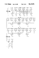
- FIGS. 2a-h show several prior art signal structures mapped on the complex plane
- FIGS. 3a, b show signal structures of the invention mapped on the complex plane
- FIGS. 4a, b are logic diagrams for implementation of the structures of FIGS. 3a, b;
- FIG. 5 is a block diagram of a differential encoder
- FIG. 6 is a block diagram of a receiver.
- the transmitted spectrum X(w) is symmetric about some center (carrier) frequency w c .
- the transmitted signal x(t) can be represented by ##EQU1## where h(t) is the impulse of a low pass filter whose cutoff frequency is half the bandwidth of the channel.
- FIG. 1 A circuit for realizing such a modulation scheme is shown in FIG. 1.
- a stream of input bits arrives at a rate of n/T bits per second, and is passed through an n-bit storage register 10.
- This pair of words controls a pair of digital-to-analog converters 14, 16, whose output voltages represent Re S i and ImS i .
- Once each T seconds this pair of D/A outputs is gated to form a pair of narrow pulses of amplitudes proportional to ReS i and ImS i .
- Each of these pulse trains is then filtered in an identical linear filter 18, 20 characterized by the impulse response h(t). Finally, the lower filter output is multiplied by sin(w c t) (the “quadrature” carrier) and subtracted from the product of the upper filter output and cos(w c t) (the "in-phase” carrier).
- This is a baseband technique; there also exist well-known methods of operating directly on the carrier itself at passband.
- An aspect of the invention involves the realization that a signal structure can be characterized by the sets of points [S i , 1 ⁇ i ⁇ M] associated with the modulation scheme, which we can map pictorially on the complex plane.
- PSK for example, the M signal points are described simply by a set of points evenly spaced around a circle.
- FIGS. 2a, 2b, and 2c illustrate 4-, 8-, and 16-phase modulation according to this method of representation.
- FIGS. 2d and 2e illustrate 4-level and 16-level QAM; it will be noted that 4-level QAM is effectively identical to 4-phase PSK in this representation, although their implementations may be quite different.
- the amplitude and phase variables are independently varied, to give for example the 4-phase and 2- or 4-amplitude structures of FIGS. 2f and 2g, or the 8-phase, 2-amplitude structure of FIG. 2h.
- h(t) will not be a perfect Nyquist waveform, and the channel will introduce additional linear distortion which will lead to intersymbol interference.
- an adaptive equalizer it is usually necessary to incorporate an adaptive equalizer to reduce intersymbol interference to an acceptable level such as is described in Proakis and Miller, IEEE Trans. Inf. Theo. Vol. IT-15, No. 4, 1969.
- phase jitter Another disturbance of importance on telephone lines is phase jitter. If a transmitted waveform x(t) is subject to phase jitter, the result is (to first order when the phase jitter is slow and channel filtering unimportant)
- ⁇ (t) is a random phase process.
- ⁇ (t) typically contains frequencies up to 180 Hz, and may have amplitude up to 30° peak-to-peak or more.
- Table 1 below gives required signal-to-noise ratios and minimum phase separations of points of the same amplitude for the signal structures of FIGS. 2a-h. (The minimum phase separation criterion above is an over-simplified, but still qualitatively indicative, measure of phase jitter immunity, since errors will actually be caused by the combined effects of noise and phase jitter.)
- FIG. 3a resembles the 4-phase, 2-amplitude structure of FIG.
- FIG. 3b resembles FIG. 2b, except that the second ring is rotated 45° with respect to the first, the third 45° with respect to the second, and the fourth 45° with respect to the third, allowing decreases in the radii of all outer rings without loss of signal-to-noise margin.
- Table II below gives required signal-to-noise ratios and minimum phase separations for the structure of FIGS. 3a and 3b.
- the savings over FIGS. 2f and 2g are 1 dB and 2.6 dB, respectively.
- a is an arbitrary complex constant.
- r.sub. 1 ⁇ r 2 ⁇ r 3 ⁇ r 4 . . . ⁇ r m thus only the innermost ring necessarily contains four points.
- FIG. 4a gives appropriate logic for the signal structure of FIG. 3a, where (B1, B2, B3) are the three input bits, (XS, X1, X2) and (YS, Y1, Y2) are two's-complement representations of the real and imaginary parts of the signal points, and the correspondence is according to the three-bit numbers associated with each signal point on the diagram of FIG. 3a.
- FIG. 4b gives logic for FIG. 3b, where (B1, B2, B3, B4) are the four input bits and (XS, X1, X2, X3) and (YS, Y1, Y2, Y3) are the coordinates of the signal points in two's-complement form, coded according to the diagram of FIG. 3b (where B1 and B2 select one of the four rings, and B3 and B4 select the phase on the ring).
- the carrier is suppressed--i.e., there is no carrier power at the frequency w c . Nonetheless there are a number of techniques by which a carrier may be derived by the receiver from the received data signal. Such techniques generally cannot distinguish between the correct phase of the received carrier and the correct phase plus multiples of 90°, due again to the 90° symmetry of the signal structure, and so may set up in any of four phases; there is said to be a 90° phase ambiguity in the recovered carrier. It is advantageous under these conditions to differentially encode the phase of the transmitted signal, by selecting the phase of the signal transmitted at time t on the basis of the bits for time t and the phase transmitted at time t-1. For example, in the eight-point structure of FIG. 3a, the two bits B2 and B3 select the phase of the transmitted signal according to
- phase ⁇ k at the time k is made equal to the phase ⁇ k-1 at time k-1 plus ⁇ (B2 k , B3 k ); i.e.,
- phase ⁇ (B2 k , B3 k ) is detected as the difference between the estimates ⁇ k and ⁇ k-1 and is unaffected by constant 90° phase rotations.
- the same differential phase technique can be used with the phase bits B3 and B4 of FIG. 3b, or indeed with any of the signal structures of the invention.
- FIG. 5 illustrates the implementation of differential encoding.
- the phase bits B2 and B3 are Gray-coded into a 2-bit integer which is added to the stored 2-bit integer ( ⁇ 1 k-1 , ⁇ 2 k-1 ) without carry--i.e., modulo 4.
- the result is an integer ( ⁇ 1 k , ⁇ 2 k ) representing the current phase, which is stored in a 2-bit memory after each sample by a clock pulse (not shown), to become the integer ( ⁇ 1 k-1 , ⁇ 2 k-1 ) for the next sample.
Landscapes
- Engineering & Computer Science (AREA)
- Computer Networks & Wireless Communication (AREA)
- Signal Processing (AREA)
- Digital Transmission Methods That Use Modulated Carrier Waves (AREA)
Abstract
Double side band-quadrature carrier modulation signal points as mapped on the complex plane are drawn from an alphabet consisting of at least 8 points, and are set up in concentric rings each rotated by 45° with respect to adjacent rings. Differential encoding is shown encoding the phase components of the transmitted signals.
Description
.Iadd.This application is a continuation of application Ser. No. 144,533, filed Apr. 28, 1980, now abandoned. .Iaddend.
This invention relates to double side band-quadrature carrier (DSB-QC) modulation. DSB-QC modulation subsumes a class of modulation techniques such as phase-shift-keying (PSK), quadrature amplitude modulation (QAM), and combined amplitude and phase modulation, such as have long been known in the art.
In high-speed data transmission across narrow-bandwidth channels such as the typical voice grade telephone channel, DSB-QC modulation has certain inherent advantages over single-sideband (SSB) and vestigial-sideband (VSB) techniques, such as are used in the majority of high-speed modems today. Against gaussian noise, it is inherently as efficient as SSB or VSB techniques in terms of the signal-to-noise ratios required to support a certain speed of transmission at a certain error rate in a given bandwidth. In addition, a coherent local demodulation carrier can be derived directly from the received data, without requiring transmission of a carrier or pilot tone. Furthermore, DSB-QC systems can be designed to have a much greater insensitivity to phase jitter on the line, or to phase error in the recovered carrier, than is possible with SSB or VSB signals.
For modest data rates, well-known modulation schemes such as four-phase modulation provide good margins against both gaussian noise and phase jitter. At higher data rates, more bits of information must be sent per signalling interval, so multi-level signalling structures of greater complexity must be used. The standard schemes mentioned above begin to degrade rapidly aginst either gaussian noise or phase jitter when more signal points are required. It is the principal purpose of the present invention to provide novel signal structures which continue to exhibit near-optimum margins against both gaussian noise and phase jitter as additional points are added. Further advantages of the invention are simplicity of implementation and of detection, suppression of carrier, and 90° symmetry, which allows use of differential phase techniques.
In general the invention features a double side band-quadrature carrier modulation system in which the signal points, as mapped on the complex plane, are drawn from an alphabet consisting of at least 8 points, and are set up in concentric rings each rotated by 45° with respect to adjacent rings. Preferred embodiments employ differential encoding of the phase components of the transmitted signals.
Other advantages and features of the invention will be apparent from the following description of a preferred embodiment thereof, taken together with the drawings, in which:
FIG. 1 is a block diagram of a DSB-QC modulation system;
FIGS. 2a-h show several prior art signal structures mapped on the complex plane;
FIGS. 3a, b show signal structures of the invention mapped on the complex plane;
FIGS. 4a, b are logic diagrams for implementation of the structures of FIGS. 3a, b;
FIG. 5 is a block diagram of a differential encoder; and
FIG. 6 is a block diagram of a receiver.
In DSB-QC modulation the transmitted spectrum X(w) is symmetric about some center (carrier) frequency wc. In digital DSB-QC, data samples dk arrive at rates of 1/T samples/second, and take on one of M values represented by a set of complex numbers Si, 1≦i≦M. Commonly M=2n, and n bits can be transmitted per sample, or n/T per second. The transmitted signal x(t) can be represented by ##EQU1## where h(t) is the impulse of a low pass filter whose cutoff frequency is half the bandwidth of the channel.
A circuit for realizing such a modulation scheme is shown in FIG. 1. A stream of input bits arrives at a rate of n/T bits per second, and is passed through an n-bit storage register 10. The n storage elements in the register are inputs to a combinational logic circuit 12 which forms one of M=2n pairs of output words; this pair of words is a digital representation of the real and imaginary parts of the Si appropriate to the n bits of input. This pair of words controls a pair of digital-to-analog converters 14, 16, whose output voltages represent Re Si and ImSi. Once each T seconds this pair of D/A outputs is gated to form a pair of narrow pulses of amplitudes proportional to ReSi and ImSi. Each of these pulse trains is then filtered in an identical linear filter 18, 20 characterized by the impulse response h(t). Finally, the lower filter output is multiplied by sin(wc t) (the "quadrature" carrier) and subtracted from the product of the upper filter output and cos(wc t) (the "in-phase" carrier). This is a baseband technique; there also exist well-known methods of operating directly on the carrier itself at passband.
An aspect of the invention involves the realization that a signal structure can be characterized by the sets of points [Si, 1≦i≦M] associated with the modulation scheme, which we can map pictorially on the complex plane. In PSK, for example, the M signal points are described simply by a set of points evenly spaced around a circle. FIGS. 2a, 2b, and 2c illustrate 4-, 8-, and 16-phase modulation according to this method of representation. In QAM, ReSi and ImSi may each take on independently one of m levels, typically equally-spaced, so that M=m2. FIGS. 2d and 2e illustrate 4-level and 16-level QAM; it will be noted that 4-level QAM is effectively identical to 4-phase PSK in this representation, although their implementations may be quite different. Finally, in combined amplitude and phase modulation, the amplitude and phase variables are independently varied, to give for example the 4-phase and 2- or 4-amplitude structures of FIGS. 2f and 2g, or the 8-phase, 2-amplitude structure of FIG. 2h.
This method of representation permits examination of the effect of distrubances on the modulated waveform x(t). We first consider an ideal case, illustrated in FIG. 6. x(t) enters the receiver and is demodulated by the two locally-generated carriers cos(wc t) and -sin(wc t). The double-frequency terms at 2 wc are removed by low- pass filters 30, 32 to recover the low pass in-phase and quadrature waveforms
ΣRed.sub.k h(t-kT)
and
ΣImd.sub.k h(t-kT).
Now suppose that h(t) is a perfect Nyquist waveform, i.e., for some time, τ, h(τ)=1, but h(τ-kT)=0 for integers k>0 or k<0. Then if we sample the two channels every T seconds at the correct times τ+kT, there will be no intersymbol interference, and we simply recover the pair of voltages Rezk =Redk and Imzk =Imdk, which tell us which bits were sent.
In a real situation, h(t) will not be a perfect Nyquist waveform, and the channel will introduce additional linear distortion which will lead to intersymbol interference. (At high data rates, it is usually necessary to incorporate an adaptive equalizer to reduce intersymbol interference to an acceptable level such as is described in Proakis and Miller, IEEE Trans. Inf. Theo. Vol. IT-15, No. 4, 1969.)
Besides intersymbol interference (which also results when the outputs are not sampled at exactly the right times), real channels introduce other degradations such as noise and nonlinearities. All of these effects tend to perturb the received pair of samples Rezk and Imzk in a random direction in the complex plane. That is, if we define the complex error ek by
e.sub.k =z.sub.k -d.sub.k,
then ek is equally likely to be a vector of any phase. Against such disturbances, therefore, we realize it to be desirable to maximize the Euclidean distance between signal points, subject to a contraint in the total signal energy E, defined as ##EQU2##
We define the required signal-to-noise margin S as 10 log10 E dB, where E is calculated for the signal points Si scaled so that the minimum Euclidean distance between any two points is 2 (so that an error can occur only if |ek |≧1).
Another disturbance of importance on telephone lines is phase jitter. If a transmitted waveform x(t) is subject to phase jitter, the result is (to first order when the phase jitter is slow and channel filtering unimportant)
x'(t)=ReΣ.sub.k d.sub.k h(t-kT) e.sup.j(w.sbsp.c.sup.t+θ(t)),
where θ(t) is a random phase process. Typically on telephone lines θ(t) contains frequencies up to 180 Hz, and may have amplitude up to 30° peak-to-peak or more. To some extent the phase jitter can be tracked at the receiver to give the locally-generated carriers cos(wc t+θ(t)) and sin(wc t+θ(t)), but there will always remain some residual phase error θe (t)=θ'(t)-θ(t). The effect of such a phase error is to rotate the received vector in the complex plane by the phase angle θek =θe (τ+kT), so that the received complex value is
z.sub.k '=e.sup.jθ.sbsp.ek.sup.) z.sub.k,
where zk is the value which would have been received had there been no phase error. It is therefore especially important that signal points be well-separated in phase.
Table 1 below gives required signal-to-noise ratios and minimum phase separations of points of the same amplitude for the signal structures of FIGS. 2a-h. (The minimum phase separation criterion above is an over-simplified, but still qualitatively indicative, measure of phase jitter immunity, since errors will actually be caused by the combined effects of noise and phase jitter.)
              TABLE I
______________________________________
          2a  2b    2c     2d  2e    2f  2g   2h
______________________________________
Required Signal-
to-Noise Ratio (dB)
            3     8.3   14.1 3   10    8.4 13.9 11.5
Phase Separation
            90°
                  45°
                        22.5°
                             90°
                                 37°
                                       90°
                                           90°
                                                45°
______________________________________
Experience has shown that on telephone lines a minimum phase separation of 45° may be insufficient to guarantee low error rates when phase jitter is severe. For M=8 or 16, this means that only the 4-phase, 2- or 4-amplitude structures of FIGS. 2f and 2g can be used. But these structures are rather inefficient in their use of power, as is shown by their values of required signal-to-noise margin in Table I.
The signal structures of the present invention retain the full 90° phase separations of the 4-phase structures, as well as their four-phase symmetry, while substantially reducing the required signal-to-noise margin over the structures of FIGS. 2f and 2g. FIG. 3a illustrates a structure according to the invention for the case M=8, and FIG. 3b, a structure for M=16. In the former case the points are at (1+j)jk and 3jk for k=0, 1, 2, 3; in the latter case they are at these eight points plus the points 3(1+j)jk and 5jk, k=0, 1, 2, 3. FIG. 3a resembles the 4-phase, 2-amplitude structure of FIG. 2f, except that the two rings have been rotated 45° with respect to one another, which allows the outer radius to be decreased without loss of signal-to-noise margin. (Actually the outer ring could be pulled in slightly more, but use of integer-valued coordinates simplifies implementation.) Similarly, FIG. 3b resembles FIG. 2b, except that the second ring is rotated 45° with respect to the first, the third 45° with respect to the second, and the fourth 45° with respect to the third, allowing decreases in the radii of all outer rings without loss of signal-to-noise margin.
Table II below gives required signal-to-noise ratios and minimum phase separations for the structure of FIGS. 3a and 3b. The savings over FIGS. 2f and 2g are 1 dB and 2.6 dB, respectively. In fact FIG. 3b is only 1.3 dB worse than the optimal FIG. 2e for M=16, but has greatly enhanced protection against phase errors.
              TABLE II
______________________________________
                  3a  3b
______________________________________
Required Signal-to
Noise Ratio (dB)    7.4   11.3
Phase Separation    90°
                          90°
______________________________________
In general, the class of structures according to the invention may be described as follows. Interest is confined to M-point structures for M≧8, since the simple 4-phase structure of FIG. 2a is entirely satisfactory for M=4. M is assumed to be a multiple of 4, as it will be if it is a power of 2. Then, m=M/4 rings of radii r1, r2, . . . rm are set up, with four points on each ring, and with each succeeding ring rotated 45° with respect to the previous one. The set {Si } may be described generally by the complex numbers ari ui jk where 1≦i≦m, 0≦k≦3, ui =1 for i even and 1+j/√2, for i odd, and a is an arbitrary complex constant. In some of the outer rings it may be acceptable to use 8-phase structures; this possibility is accounted for by the requirement r.sub. 1 <r2 ≦r3 ≦r4 . . . ≦rm ; thus only the innermost ring necessarily contains four points.
Implementation of the invention is straight-forward. The circuit of FIG. 1 can be used with appropriate combinational logic to generate the integers 0, +1, +3, or +5 in ordinary two's-complement form, which can then drive standard 3- or 4-bit D/A converters. FIG. 4a gives appropriate logic for the signal structure of FIG. 3a, where (B1, B2, B3) are the three input bits, (XS, X1, X2) and (YS, Y1, Y2) are two's-complement representations of the real and imaginary parts of the signal points, and the correspondence is according to the three-bit numbers associated with each signal point on the diagram of FIG. 3a. (In this correspondence B1 is in effect an amplitude variable denoting inner or outer ring, whereas B2 and B3 select one of the four phases.) Similarly FIG. 4b gives logic for FIG. 3b, where (B1, B2, B3, B4) are the four input bits and (XS, X1, X2, X3) and (YS, Y1, Y2, Y3) are the coordinates of the signal points in two's-complement form, coded according to the diagram of FIG. 3b (where B1 and B2 select one of the four rings, and B3 and B4 select the phase on the ring).
Because of the four-phase symmetry of these structures, the carrier is suppressed--i.e., there is no carrier power at the frequency wc. Nonetheless there are a number of techniques by which a carrier may be derived by the receiver from the received data signal. Such techniques generally cannot distinguish between the correct phase of the received carrier and the correct phase plus multiples of 90°, due again to the 90° symmetry of the signal structure, and so may set up in any of four phases; there is said to be a 90° phase ambiguity in the recovered carrier. It is advantageous under these conditions to differentially encode the phase of the transmitted signal, by selecting the phase of the signal transmitted at time t on the basis of the bits for time t and the phase transmitted at time t-1. For example, in the eight-point structure of FIG. 3a, the two bits B2 and B3 select the phase of the transmitted signal according to
d.sub.k =d(B1.sub.k)e.sup.jθ(B2.sbsp.k.sup.,B3.sbsp..sup.)
where d(0)=(1+j) and d(1)=3, while θ(0,0)=0, θ(0, 1)=π/2, θ(1,1)=π, and θ(1,0)=3π/2, and B1k, B2k and B3k represent the values of the three input bits at time k. If instead the phase is differentially encoded then the phase θk at the time k is made equal to the phase θk-1 at time k-1 plus θ(B2k, B3k); i.e.,
θ.sub.k =θ.sub.k-1 +θ(B2.sub.k,B3.sub.k)
d.sub.k =d(B1.sub.k)e.sup.jθ.sbsp.k
Then at the receiver the phase θ(B2k, B3k) is detected as the difference between the estimates θk and θk-1 and is unaffected by constant 90° phase rotations. The same differential phase technique can be used with the phase bits B3 and B4 of FIG. 3b, or indeed with any of the signal structures of the invention.
FIG. 5 illustrates the implementation of differential encoding. The phase bits B2 and B3 are Gray-coded into a 2-bit integer which is added to the stored 2-bit integer (θ1k-1, θ2k-1) without carry--i.e., modulo 4. The result is an integer (θ1k, θ2k) representing the current phase, which is stored in a 2-bit memory after each sample by a clock pulse (not shown), to become the integer (θ1k-1, θ2k-1) for the next sample. The integer is also Gray-decoded to form a (B2',B3') which can be used instead of (B2, B3) as the input to the combinational logic of FIG. 4a. [Note that when (θ1k-1, θ2k-1)=(0, 0)(B2',B3')=(B2, B3).]
Other embodiments are within the following claims:
Claims (9)
1. A double side band-quadrature carrier modulation system comprising
input means for receiving a sequence of symbols ak at a rate 1/T per second.
coding means connected to said input means for providing from said symbbols a sequence of complex valued signal points dk drawn from an alphabet comprising M points arranged in a multiplicity of concentric rings in the complex plane including an innermost ring having four equally spaced points and a plurality of additional rings each having four equally spaced points, each said ring being rotated by 45° with respect to adjacent said rings, and
modulating means connected to said coding means for providing from said signal points a signal in the form ##EQU3## where h(t-kT) represents an impulse response, wc represents a carrier frequency, t represents time, j equals √-1, and k is the index of dk and ak wherein said coding means includes means for effectively providing said signal points arranged in at least four concentric rings in the complex plane. .[.
2. The system of claim 1 wherein said coding means includes means for effectively providing said signal points arranged in at least four concentric rings in the complex plane..].
3. The system of claim .[.2.]. .Iadd.1 .Iaddend.wherein said coding means includes means for causing the innermost four said rings to have radii in the ratio √2:3:3√2:5.
4. The system of claim 1 wherein said coding means includes means for causing the phase component of each dk to depend upon ak and upon the phase component of d.sub.(k-1).
5. The system of claim 1 wherein said coding means includes means for causing each said dk to have integer valued coordinates in the complex plane.
6. A double side band-quadrature carrier modulation system comprising
input means for receiving a sequence of symbols ak at a rate 1/T per second,
coding means connected to said input means for providing from said symbols a sequence of complex valued signal points dk drawn from an alphabet comprising M points arranged in a multiplicity of concentric rings in the complex plane including an innermost ring having four equally spaced points and .[.a plurality of.]. .Iadd.at least three .Iaddend.additional rings having four equally spaced points, each said ring being rotated by 45° with respect to adjacent said rings, and
filtering means connected to said coding means for providing from said signal points the real and imaginary parts of a complex valued baseband signal in the form ##EQU4## and modulating means connected to said filtering means for providing from said baseband signal a passband signal in the form ##EQU5## where h(t-kT) represents an impulse response, wc represents a carrier frequency, t represents time, j equals √-1, and k is the index of dk and ak.
7. A double side band-quadrature carrier modulation method comprising
receiving a sequence of symbols ak at a rate 1/T per second
providing from said symbols a sequence of complex valued signal points dk drawn from an alphabet comprising M points arranged in a multiplicity of concentric rings in the complex plane including an innermost ring having four equally spaced points and .[.a plurality of.]. .Iadd.at least three .Iaddend.additional rings each having four equally spaced points, each said ring being rotated by 45° with respect to adjacent said rings, and
providing from said signal points a signal in the form ##EQU6## where h(t-kT) represents an impulse response, wc represents a carrier frequency, t represents time, j equals √-1, and k is the index of dk and ak.
8. A double side band-quadrature carrier modulation method comprising
receiving a sequence of symbols ak at a rate 1/T per second,
providing from said symbols a sequence of complex valued signal points dk drawn from an alphabet comprising M points arranged in a multiplicity of concentric rings in the complex plane including an innermost ring having four equally spaced points and .[.a plurality of.]. .Iadd.at least three .Iaddend.additional rings having four equally spaced points, each said ring being rotated by 45° with respect to adjacent said rings, and
providing from said signal points the real and imaginary parts of a complex valued baseband signal in the form ##EQU7## and providing from said baseband signal a passband signal in the form ##EQU8## where h(t-kT) represents an impulse response, wc represents a carrier frequency, t represents time, j equals √-1, and k is the index of dk and ak wherein said coding means includes means for effectively providing said signal points arranged in at least four concentric rings in the complex plane. .Iadd.
9. The system of claim 1 wherein said coding means includes means for providing signal points from an alphabet of sixteen points arranged in exactly four concentric rings in the complex plane. .Iaddend.
Priority Applications (1)
| Application Number | Priority Date | Filing Date | Title |
|---|---|---|---|
| US06/621,127 USRE33056E (en) | 1971-09-14 | 1984-06-15 | Signal structures for double side band-quadrature carrier modulation |
Applications Claiming Priority (3)
| Application Number | Priority Date | Filing Date | Title |
|---|---|---|---|
| US180289A US3887768A (en) | 1971-09-14 | 1971-09-14 | Signal structures for double side band-quadrature carrier modulation |
| US14453380A | 1980-04-28 | 1980-04-28 | |
| US06/621,127 USRE33056E (en) | 1971-09-14 | 1984-06-15 | Signal structures for double side band-quadrature carrier modulation |
Related Parent Applications (2)
| Application Number | Title | Priority Date | Filing Date |
|---|---|---|---|
| US180289A Reissue US3887768A (en) | 1971-09-14 | 1971-09-14 | Signal structures for double side band-quadrature carrier modulation |
| US14453380A Continuation | 1971-09-14 | 1980-04-28 |
Publications (1)
| Publication Number | Publication Date |
|---|---|
| USRE33056E true USRE33056E (en) | 1989-09-12 |
Family
ID=27386114
Family Applications (1)
| Application Number | Title | Priority Date | Filing Date |
|---|---|---|---|
| US06/621,127 Expired - Lifetime USRE33056E (en) | 1971-09-14 | 1984-06-15 | Signal structures for double side band-quadrature carrier modulation |
Country Status (1)
| Country | Link |
|---|---|
| US (1) | USRE33056E (en) |
Cited By (5)
| Publication number | Priority date | Publication date | Assignee | Title |
|---|---|---|---|---|
| US5177455A (en) * | 1992-01-22 | 1993-01-05 | Mpr Teltech Ltd. | Digital phase and amplitude modulator |
| US5263052A (en) * | 1991-09-30 | 1993-11-16 | Motorola, Inc. | Viterbi equalizer for radio receiver |
| US5515400A (en) * | 1989-02-17 | 1996-05-07 | Fujitsu Limited | Method for arranging signal points in a quadrature amplitude modulation/demodulation system |
| US6553535B1 (en) | 1998-08-21 | 2003-04-22 | Massachusetts Institute Of Technology | Power-efficient communication protocol |
| US20030115533A1 (en) * | 1998-08-21 | 2003-06-19 | Asada Haruhiko H. | Source coding for interference reduction |
Citations (6)
| Publication number | Priority date | Publication date | Assignee | Title |
|---|---|---|---|---|
| US3123670A (en) * | 1964-03-03 | Filter | ||
| US3614622A (en) * | 1968-04-30 | 1971-10-19 | Codex Corp | Data transmission method and system |
| US3619501A (en) * | 1969-06-27 | 1971-11-09 | Ibm | Multiphase modulated transmission encoder |
| US3619503A (en) * | 1969-11-18 | 1971-11-09 | Int Communications Corp | Phase and amplitude modulated modem |
| US3706945A (en) * | 1970-08-14 | 1972-12-19 | Kokusai Denshin Denwa Co Ltd | Amplitude-modulated eight-phase phase-modulation system |
| US3878468A (en) * | 1974-01-30 | 1975-04-15 | Bell Telephone Labor Inc | Joint equalization and carrier recovery adaptation in data transmission systems |
-
1984
- 1984-06-15 US US06/621,127 patent/USRE33056E/en not_active Expired - Lifetime
Patent Citations (6)
| Publication number | Priority date | Publication date | Assignee | Title |
|---|---|---|---|---|
| US3123670A (en) * | 1964-03-03 | Filter | ||
| US3614622A (en) * | 1968-04-30 | 1971-10-19 | Codex Corp | Data transmission method and system |
| US3619501A (en) * | 1969-06-27 | 1971-11-09 | Ibm | Multiphase modulated transmission encoder |
| US3619503A (en) * | 1969-11-18 | 1971-11-09 | Int Communications Corp | Phase and amplitude modulated modem |
| US3706945A (en) * | 1970-08-14 | 1972-12-19 | Kokusai Denshin Denwa Co Ltd | Amplitude-modulated eight-phase phase-modulation system |
| US3878468A (en) * | 1974-01-30 | 1975-04-15 | Bell Telephone Labor Inc | Joint equalization and carrier recovery adaptation in data transmission systems |
Non-Patent Citations (32)
| Title |
|---|
| A. Lubarsky, Jr., Proceedings of the National Electronics Conference, vol. XXVI, pp. 942 945, Dec. 1970. * |
| A. Lubarsky, Jr., Proceedings of the National Electronics Conference, vol. XXVI, pp. 942-945, Dec. 1970. |
| American Telephone and Telegraph Co., "Transmission Specifications for Voice Grade Private Line Data Channels", Mar. 1969. |
| American Telephone and Telegraph Co., Transmission Specifications for Voice Grade Private Line Data Channels , Mar. 1969. * |
| Bell System Technical Reference, "Data Communications Using Voiceband Private Line Channels", pp. 1-51 & A1-A16, Oct. 1973. |
| Bell System Technical Reference, Data Communications Using Voiceband Private Line Channels , pp. 1 51 & A1 A16, Oct. 1973. * |
| C. M. Thomas, "International Telemetering Conference", pp. 289-300, Oct. 10-11-12, 1972. |
| C. M. Thomas, International Telemetering Conference , pp. 289 300, Oct. 10 11 12, 1972. * |
| C. N. Campopiano et al, IRE Transactions on Comm. Systems, vol. CS 10, No. 1, pp. 90 95, Mar. 1962. * |
| C. N. Campopiano et al, IRE Transactions on Comm. Systems, vol. CS-10, No. 1, pp. 90-95, Mar. 1962. |
| C. R. Cahn, IRE Transactions on Comm. Systems, vol. CS 8, No. 1, pp. 150 155, Sep. 1960. * |
| C. R. Cahn, IRE Transactions on Comm. Systems, vol. CS-8, No. 1, pp. 150-155, Sep. 1960. |
| CCITT Sixth Plenary Assembly, "9600 Bits per Second Modem Standardized for Use on Leased Telephone-Type Circuits", Orange Book, vol. VIII.1, pp. 143-153, Sep.-Oct. 1977. |
| CCITT Sixth Plenary Assembly, 9600 Bits per Second Modem Standardized for Use on Leased Telephone Type Circuits , Orange Book, vol. VIII.1, pp. 143 153, Sep. Oct. 1977. * |
| CCITT; Special Study Group A Contribution No. 92, DSB Modulation as a Preferred Technique . . . , pp. 1 28, Aug. 1974. * |
| CCITT; Special Study Group A-Contribution No. 92, "DSB Modulation as a Preferred Technique . . . ", pp. 1-28, Aug. 1974. |
| Codex Corporation, letter to Auerbach Information, Inc., Re, Announcing New 4800 bps Modem, 2 pages, 14 Sep. 1970. * |
| Codex Corporation, Statement on Patents and Patent Licensing, Contribution No. 221, CCITT Special Study Group A, Dec. 1975. * |
| G. J. Foschini et al; Bell System Technical Journal, vol. 52, No. 6, pp. 927 965, Jul. Aug. 1973. * |
| G. J. Foschini et al; Bell System Technical Journal, vol. 52, No. 6, pp. 927-965, Jul.-Aug. 1973. |
| Hancock, J. C., Lucky, R. W., "Performance of Combined Amplitude and Phase Modulated Communications Systems", IRE Trans. on Comm. Sys., vol. CS-8, pp. 232-237, Dec. 1960. |
| Hancock, J. C., Lucky, R. W., Performance of Combined Amplitude and Phase Modulated Communications Systems , IRE Trans. on Comm. Sys., vol. CS 8, pp. 232 237, Dec. 1960. * |
| J. Salz, Bell System Technical Journal, vol. 50, No. 7, pp. 2399 2419, Sep. 1971. * |
| J. Salz, Bell System Technical Journal, vol. 50, No. 7, pp. 2399-2419, Sep. 1971. |
| N. I. Nasell, Bell System Technical Journal, vol. 47, No. 6, pp. 1001 1018, Jul. Aug. 1968. * |
| N. I. Nasell, Bell System Technical Journal, vol. 47, No. 6, pp. 1001-1018, Jul.-Aug. 1968. |
| R. W. Lucky et al, IRE Transactions on Comm. Systems, vol. CS 10, No. 2, pp. 185 192, Jun. 1962. * |
| R. W. Lucky et al, IRE Transactions on Comm. Systems, vol. CS-10, No. 2, pp. 185-192, Jun. 1962. |
| R. W. Lucky et al, Principles of Data Communications; McGraw Hill Book Company, 1968. * |
| R. W. Lucky et al, Principles of Data Communications; McGraw-Hill Book Company, 1968. |
| R. W. Lucky, "Digital Phase and Amplitude Modulated Communication Systems", Doctoral Thesis, Purdue University, Aug. 1961. |
| R. W. Lucky, Digital Phase and Amplitude Modulated Communication Systems , Doctoral Thesis, Purdue University, Aug. 1961. * |
Cited By (6)
| Publication number | Priority date | Publication date | Assignee | Title |
|---|---|---|---|---|
| US5515400A (en) * | 1989-02-17 | 1996-05-07 | Fujitsu Limited | Method for arranging signal points in a quadrature amplitude modulation/demodulation system |
| US5263052A (en) * | 1991-09-30 | 1993-11-16 | Motorola, Inc. | Viterbi equalizer for radio receiver |
| US5177455A (en) * | 1992-01-22 | 1993-01-05 | Mpr Teltech Ltd. | Digital phase and amplitude modulator |
| US6553535B1 (en) | 1998-08-21 | 2003-04-22 | Massachusetts Institute Of Technology | Power-efficient communication protocol |
| US20030115533A1 (en) * | 1998-08-21 | 2003-06-19 | Asada Haruhiko H. | Source coding for interference reduction |
| US7376105B2 (en) | 1998-08-21 | 2008-05-20 | Massachusetts Institute Of Technology | Source coding for interference reduction |
Similar Documents
| Publication | Publication Date | Title |
|---|---|---|
| US3887768A (en) | Signal structures for double side band-quadrature carrier modulation | |
| US4123710A (en) | Partial response QAM modem | |
| CA1212419A (en) | Differentially nonlinear convolutional channel coding with expanded set of signalling alphabets | |
| US4483012A (en) | Differentially convolutional channel coding with expanded set of signalling alphabets | |
| Anderson et al. | Digital phase modulation | |
| US4720839A (en) | Efficiency data transmission technique | |
| US3983485A (en) | Multi-phase and multi-amplitude level modulator and modulation and demodulation methods | |
| US3760277A (en) | Coding and decoding system with multi-level format | |
| US4457004A (en) | Multidimensional channel coding | |
| US6137829A (en) | System and method for transmitting special marker symbols | |
| US3727136A (en) | Automatic equalizer for phase-modulation data transmission systems | |
| US3988539A (en) | Data transmission system using optimal eight-vector signaling scheme | |
| US4739413A (en) | Video-optimized modulator-demodulator with adjacent modulating amplitudes matched to adjacent pixel gray values | |
| US3423529A (en) | Automatic phase recovery in suppressed carrier quadrature modulated biternary communication systems | |
| US5734681A (en) | Process and system for transferring vector signal with precoding for signal power reduction | |
| US4562425A (en) | Differential encoder and decoder for transmitting binary data | |
| USRE33056E (en) | Signal structures for double side band-quadrature carrier modulation | |
| JPS58130658A (en) | Modulator/demodulator set for digital communication | |
| EP0206572B1 (en) | Video optimized modulator-demodulator | |
| US6278741B1 (en) | Timing recovery circuit in QAM modems | |
| JPS60134545A (en) | Data communication signal structure | |
| Lender | Correlative data transmission with coherent recovery using absolute reference | |
| US6009123A (en) | Process and system for transferring vector signal with precoding for signal power reduction | |
| US7469022B2 (en) | Methods and apparatus for symmetrical phase-shift keying | |
| JPH0748677B2 (en) | Equalizer |
Legal Events
| Date | Code | Title | Description |
|---|---|---|---|
| AS | Assignment |
Owner name: MOTOROLA, INC., ILLINOIS Free format text: MERGER (EFFECTIVE 12-31-94).;ASSIGNOR:CODEX CORPORATION;REEL/FRAME:007268/0432 Effective date: 19941216 |