USRE35614E - Process for improved quality of CVD copper films - Google Patents
Process for improved quality of CVD copper films Download PDFInfo
- Publication number
- USRE35614E USRE35614E US08/667,254 US66725496A USRE35614E US RE35614 E USRE35614 E US RE35614E US 66725496 A US66725496 A US 66725496A US RE35614 E USRE35614 E US RE35614E
- Authority
- US
- United States
- Prior art keywords
- copper
- ligand
- cvd
- reactor
- films
- Prior art date
- Legal status (The legal status is an assumption and is not a legal conclusion. Google has not performed a legal analysis and makes no representation as to the accuracy of the status listed.)
- Expired - Lifetime
Links
Images


Classifications
-
- C—CHEMISTRY; METALLURGY
- C23—COATING METALLIC MATERIAL; COATING MATERIAL WITH METALLIC MATERIAL; CHEMICAL SURFACE TREATMENT; DIFFUSION TREATMENT OF METALLIC MATERIAL; COATING BY VACUUM EVAPORATION, BY SPUTTERING, BY ION IMPLANTATION OR BY CHEMICAL VAPOUR DEPOSITION, IN GENERAL; INHIBITING CORROSION OF METALLIC MATERIAL OR INCRUSTATION IN GENERAL
- C23C—COATING METALLIC MATERIAL; COATING MATERIAL WITH METALLIC MATERIAL; SURFACE TREATMENT OF METALLIC MATERIAL BY DIFFUSION INTO THE SURFACE, BY CHEMICAL CONVERSION OR SUBSTITUTION; COATING BY VACUUM EVAPORATION, BY SPUTTERING, BY ION IMPLANTATION OR BY CHEMICAL VAPOUR DEPOSITION, IN GENERAL
- C23C16/00—Chemical coating by decomposition of gaseous compounds, without leaving reaction products of surface material in the coating, i.e. chemical vapour deposition [CVD] processes
- C23C16/06—Chemical coating by decomposition of gaseous compounds, without leaving reaction products of surface material in the coating, i.e. chemical vapour deposition [CVD] processes characterised by the deposition of metallic material
- C23C16/18—Chemical coating by decomposition of gaseous compounds, without leaving reaction products of surface material in the coating, i.e. chemical vapour deposition [CVD] processes characterised by the deposition of metallic material from metallo-organic compounds
Definitions
- the present invention relates to Chemical Vapor Deposition (CVD) copper films deposited onto either conducting metallic or insulating surfaces.
- CVD Chemical Vapor Deposition
- Metal interconnects also need to provide the lowest electrical resistance path possible since resistance-capacitance delays become a dominant factor in circuit performance at sub half micron levels.
- the aluminum that is widely used in present day interconnect manufacturing is reasonably conductive (2.7 microhm cm), but needs to be alloyed with 0.5 to 4.0% Cu to minimize the electromigration tendencies of the pure metal.
- Tungsten also widely used, is electromigration resistant but is of higher resistivity (5.4 microhm cm). Considering these facts, copper should be an excellent interconnect metal as it is both highly conductive (1.7 microhm cm) and electromigration resistant.
- Metallic interconnects are typically horizontal lines (runners) or plugs (vias) that wire together devices in microprocessors. At feature sizes of >1 micron these metallic components can be built into the microcircuits by PVD (Physical Vapor Deposition) techniques such as sputtering or evaporation. In essence PVD consists of condensing a metal vapor onto a surface/cp systemdict/curr or channel of a circuit where an electrical connection needs to be formed. Since this is a non-selective metallization, either a postdeposition clean-up (i.e. etch-back) or a predeposition masking of the substrate (i.e. the lift-off technique) is required in order to prepare individual discrete metal components.
- PVD Physical Vapor Deposition
- CVD Chemical Vapor Deposition
- a volatile metal-organic compound in the gas phase is contacted with areas of a circuit where growth of metal film (i.e. interconnect) is required.
- a surface catalyzed chemical reaction then occurs which leads to deposition of the desired metal. Since this is a chemical reaction, there is potential for it to provide surface selective melallization. That is, CVD metal deposition can be made to occur at only specific locations compared to the non-selective PVD processes. Also, since the metal film steadily grows on the desired surface it is of a uniform thickness and highly conformal even to severe geometrics. In this respect CVD is naturally suited to fabricating submicron high aspect ratio features.
- An example of a currently available selective CVD metallization is the deposition of tungsten onto a silicon surface using tungsten hexafluoride as the volatile organometallic precursor (see T. Ohba, et al., "Tungsten and Other Advanced Metals for VLSI/ULSI Applications V,” Ed. by S. S. Wong and S. Furukawa, MRS, Pittsburgh, Pa., 273 (1990).
- the chemistry that drives this process can be divided into two steps. Initially the WF 6 reacts with the elemental silicon surface to yield tungsten metal and volatile silicon hexafluoride. Hydrogen gas is then added to the system which reduces further WF 6 at the freshly formed metal surface thereby yielding additional tungsten and HF gas.
- Desirable selectivities for a copper CVD process include deposition onto conducting metallic or metallic like surfaces such as tungsten, tantalum, or titanium nitride versus insulating surfaces such as silicon oxide. These metallic surfaces provide a diffusion barrier between the CVD copper and the underlying silicon substrate that the device is grown upon.
- Copper films have previously been prepared via CVD using various copper precursors. Most of these compounds will only deposit copper metal at temperatures higher than 200° C. Historically, the best known and most frequently used CVD copper precursor is the solid compound copper +2 bis(hexafluoroacetylacetonate). This highly fluorinated organometallic precursor is significantly more volatile than its parent unfluorinated complex copper +2 bis(acetylacetonate) and its ease of vaporization readily lends this compound towards CVD processes. The use of this compound as a general precursor for CVD copper metallization was first described by R. L. VanHemert et al. J. Electrochem. Soc. (112), 1123 (1965) and by R. W. Moshier et al. U.S. Pat.
- the copper +2 (hfac) 2 is simply pyrolyzed to give copper metal and fragments of the hfac ligand. Pure copper is generally reported for hydrogen reductions but oxygen and carbon are found in the films obtained by pyrolysis. Copper films have also been prepared from copper +2 (hfac) 2 by plasma enhanced deposition, C. Oehr, H. Suhr, Appl. Phy. A. (45) 151-154 (1988), laser photothermal decomposition, F. A. Houle; C. R. Jones; T. Baum; C. Pico; C,. A. Korae; Appl. Phys Lett.
- a particularly effective CVD copper precursor is 1,1,1,5,5,5-hexafluoro-2,4-pentanedionato-copper (I) trimethylvinylsilane sold under the trademark CupraSelect by the Schumacher unit of Air Products and Chemicals, Inc., Carlsbad, Calif. This compound, Cu(hfac)(TMVS), is known to deposit quality copper films.
- a method for chemical vapor deposition of improved quality copper films by introducing into a CVD reactor vapors of an organometallic copper complex, e.g. 1,1,1,5,5,5-hexafluoro-2,4-pentanedionato copper(I) trimethylvinylsilane together with at least one percent (1%) by volume of the volume of copper complex vapors of a volatile ligand or ligand hydrate.
- an organometallic copper complex e.g. 1,1,1,5,5,5-hexafluoro-2,4-pentanedionato copper(I) trimethylvinylsilane together with at least one percent (1%) by volume of the volume of copper complex vapors of a volatile ligand or ligand hydrate.
- the volatile ligand . .or ligand hydrate.! The volatile ligand . .or ligand hydrate.!.
- R 1 , R 3 , R 4 , and R 5 are alkyl, aryl, fluoroalkyl or fluoroaryl;
- R 2 is .Iadd.hydrogen.Iaddend., halogen, alkyl, aryl, fluoroalkyl or fluoroaryl;
- X and Y are selected so that when X ⁇ . .0.!. .Iadd.O.Iaddend., Y can be OH, NH 2 or N(R 4 )H, when X ⁇ NH, Y can be NH 2 or N(R 4 )H, when X ⁇ NR 5 , Y can be N(R 4 )H.
- Useful stable volatile hydrate of these ligands can also be used. These are compounds that contain between one and six molecules of reversibly chemically bound water molecules per molecule of ligand. In some cases it may not be desirable to mix the hydrate of the ligand and the copper complex prior to introduction into the deposition chamber.
- organometalic copper complexes suitable for this present invention of the formula shown below: ##STR2##
- R 1 , and R 3 can be alkyl, fluoroalkyl, aryl, fluoroaryl and R 2 alkyl, fluoroalkyl, aryl, fluoroaryl or halogen and L is a nonaromatic unsaturated ligand such as alkene or alkyne.
- L is a nonaromatic unsaturated ligand such as alkene or alkyne.
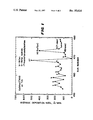
- FIG. 1 is a plot of deposition rate for twenty seven CVD depositions of Cu(hfac)TMVS on titanium nitride substrates showing the effect of using this invention on selected runs.
- FIG. 2 is a plot of deposition rate against percentage addition of Hhfac to the Cu(hrac)TMVS precursor during deposition of copper on platinum, titanium nitride and gold-chromium alloy substrates.
- FIG. 3 is a reproduction of four copper film thickness maps used to illustrate this invention.
- Copper films grown by the invention herein disclosed also show excellent substrate edge to edge uniformity of film thickness that is superior to the uniformity achieved without the ligand addition as disclosed in this invention. Uniform deposition is particularly important to the semiconductor industry since it allows each device on the surface of a production wafer to receive an identical uniform layer of metal.
- this invention leads to an enhanced rate of copper deposition onto selected substrates.
- This accelerated deposition rate is highly desirable since it reduces the overall CVD processing time that is required to grow the needed thickness of copper. Since this higher rate stems from a more efficient utilization of the precursor under CVD processing conditions, the quantity and hence the cost of precursor consumed per wafer is also reduced.
- This invention is practiced by evaporating the ligand or ligand hydrate under reduced pressure and introducing this vapor into the CVD process chamber along with vapors of the copper precursor. If there is no chemical incompatibility of the ligand and complex copper, the ligand can be directly mixed with the copper precursor to form a solution and this solution injected directly into a low pressure evaporation chamber. If a solid copper precursor is used, the addition of an inert solvent may be required to bring the precursor and ligand into solution. The resulting mixed vapor of copper precursor and ligand is then introduced into the CVD chamber. Various inert carrier gases such as argon, nitrogen or helium can be used to transport the copper precursor or ligand vapors into the CVD reactor.
- argon, nitrogen or helium can be used to transport the copper precursor or ligand vapors into the CVD reactor.
- Hhfac 1,1,1,5,5,5-hexafluoro-2,4-pentanedione.
- Hhfac is the protonated "free ligand" of the hfac anion found in all "hfac" compounds. Since Hhfac is known to be an etchant of metal containing surfaces (Norman et al U.S. Pat. No.
- Hhfac hydrate (1,1,1,5,5,5-hexafluoro-2,4-pentanedione . .dehydrate.!. .Iadd.dihydrate .Iaddend. was prepared by adding 3.6 g water (0.2 moles) dropwise over a period of 10 minutes with stirring to a solution of 20.8 g of hexafluoro-acetylacetone (0.1 moles) dissolved in 300 ml of diethyl ether. The mixture was then stirred for an additional 30 minutes at room temperature. The ether was then stripped off under vacuum and the resulting solid twice sublimed under dynamic vacuum at 40° C./20 millitorr pressure.
- a custom-built Vactronics coldwall stainless steel reactor fitted with a load lock was used for these studies.
- Helium carrier gas was used to transport precursor vapors into the CVD reactor by bubbling through a 200 g charge of CupraSelect precursor housed in a stainless steel vessel at 36° C. Prior to loading this vessel it was dried by heating to 220° C. under a dynamic vacuum of 20 millitorr for 4 hours. A liquid nitrogen cryogenic trap was connected between the bubbler and the vacuum pump to trap outgassing water. 40 sccm of He carrier gas were used in each run. The average duration of each run was 10 minutes. Wafer temperatures were set at 160° C.
- Hhfac results in an increase in the rate and a return to smoother films as indicated by stylus profilometry.
- Run 471 did not show a large decrease in deposition rate but the film was noticeably rougher than run 470.
- Addition of Hhfac hydrate in run 472 gave a small increase in rate and a smoother film than 471. As more Hhfac hydrate was added the rate increased and the increase appeared to be proportional to the mount of Hhfac hydrate added to the reactor.
- FIG. 3 shows four copper films thickness maps, as determined by the sheet resistivity (blanket areas) and stylus profilometry (patterned areas) of the copper films when processed with or without Hhfac. All other deposition conditions (wafer temperature 160° C., 40 sccm He carrier gas, precursor temperature 36° C., 500 milli-Torr chamber pressure) for the Hhfac vs. no Hhfac samples were identical.
- the upper left hard quadrant shows depositions of copper on a platinum substrate with no addition of Hhfac to the precursor.
- the resulting film had an average thickness of 2,403 angstrom units with a standard deviation in thickness ( ⁇ ) of 196 angstrom units or a uniformity of ⁇ 14.8%.
- Table 1 indicates how the reflectivity of the copper films processed in the presence of added Hhfac ligand is consistently higher than those films processed in the absence of added Hhfac ligand.
- These reflectance values for copper films are, also controlled by the underlying metal film. That is, smoother base films will result in higher reflectances.
- the base films for Hhfac vs. no Hhfac came from the same metallized wafers.
- the addition of Hhfac has improved the reflectance by reducing the surface roughnesses; rougher films will have lower reflection coefficients.
- the substrate can be heated to temperatures between 120° C. and 350° C.
- the reactor can be operated at a pressure of between 10 mTorr and 100 Torr and the copper precursor vapors introduced via an inert carrier gas such as helium, argon, nitrogen, neon xenon, krypton and mixtures thereof introduced into the CVD reactor at a rate of from 1 to 1000 sccm.
- an inert carrier gas such as helium, argon, nitrogen, neon xenon, krypton and mixtures thereof introduced into the CVD reactor at a rate of from 1 to 1000 sccm.
- ligand or ligand hydrate used with the present invention are hexafluoroaceytlacetone, heptafluoroacetylacetone or hexafluoroacetylacetone dehydrate.
- the present invention is a process for improving the overall quality of copper films fabricated by chemical vapor deposition(CVD) from organometallic copper complexes. This is achieved by blending vapors of either ligands or their hydrates with vapors of the copper precursor as it is utilized in the CVD metallization.
- CVD chemical vapor deposition
- This substrate would typically be a silicon wafer of the type used in microelectronic semiconductor manufacturing.
Abstract
Chemical Vapor Deposition of copper films is enhanced by simultaneously introducing in the reactor vapor of an organometalic copper precursor and . .copper complex.!. vapor of a volatile ligand or the hydrate of the ligand.
Description
The present invention relates to Chemical Vapor Deposition (CVD) copper films deposited onto either conducting metallic or insulating surfaces.
In the electronics industry there is a steady trend towards manufacturing integrated circuitry of increasingly higher speed and larger information storage capacity. This requires the individual electrical devices such as transistors, etc. within the integrated circuitry to be fabricated at an increasingly small scale. The metallic electrical interconnects between the devices also need to be miniaturized. As device and interconnect dimensions approach one-half to one-quarter of a micron, the choice of interconnect metal becomes critical. The large current densities resulting from small interconnect cross sectional areas can lead to major problems such as electromigration, mess migration and voiding where the metal lines become fractured or otherwise physically degraded under operating conditions, a major drawback with aluminum alloys. Metal interconnects also need to provide the lowest electrical resistance path possible since resistance-capacitance delays become a dominant factor in circuit performance at sub half micron levels. The aluminum that is widely used in present day interconnect manufacturing is reasonably conductive (2.7 microhm cm), but needs to be alloyed with 0.5 to 4.0% Cu to minimize the electromigration tendencies of the pure metal. Tungsten, also widely used, is electromigration resistant but is of higher resistivity (5.4 microhm cm). Considering these facts, copper should be an excellent interconnect metal as it is both highly conductive (1.7 microhm cm) and electromigration resistant.
Metallic interconnects are typically horizontal lines (runners) or plugs (vias) that wire together devices in microprocessors. At feature sizes of >1 micron these metallic components can be built into the microcircuits by PVD (Physical Vapor Deposition) techniques such as sputtering or evaporation. In essence PVD consists of condensing a metal vapor onto a surface/cp systemdict/curr or channel of a circuit where an electrical connection needs to be formed. Since this is a non-selective metallization, either a postdeposition clean-up (i.e. etch-back) or a predeposition masking of the substrate (i.e. the lift-off technique) is required in order to prepare individual discrete metal components. However, the severe surface topographies presented by sub-micron features preclude the effective use of PVD since this "line of sight" technique cannot provide a uniform conformal coating on such high aspect ratio highly convoluted surfaces. Specific examples of these shortcomings include the phenomena of geometrical shadowing and poor step coverage.
A superior process for producing these microscopic metal features is CVD (Chemical Vapor Deposition). In this technique a volatile metal-organic compound in the gas phase is contacted with areas of a circuit where growth of metal film (i.e. interconnect) is required. A surface catalyzed chemical reaction then occurs which leads to deposition of the desired metal. Since this is a chemical reaction, there is potential for it to provide surface selective melallization. That is, CVD metal deposition can be made to occur at only specific locations compared to the non-selective PVD processes. Also, since the metal film steadily grows on the desired surface it is of a uniform thickness and highly conformal even to severe geometrics. In this respect CVD is naturally suited to fabricating submicron high aspect ratio features.
An example of a currently available selective CVD metallization is the deposition of tungsten onto a silicon surface using tungsten hexafluoride as the volatile organometallic precursor (see T. Ohba, et al., "Tungsten and Other Advanced Metals for VLSI/ULSI Applications V," Ed. by S. S. Wong and S. Furukawa, MRS, Pittsburgh, Pa., 273 (1990). The chemistry that drives this process can be divided into two steps. Initially the WF6 reacts with the elemental silicon surface to yield tungsten metal and volatile silicon hexafluoride. Hydrogen gas is then added to the system which reduces further WF6 at the freshly formed metal surface thereby yielding additional tungsten and HF gas. However, loss of selectivity can be observed and is commonly ascribed to the corrosive nature of HF. T. Ohba, et al., Tech. Dig. IEDM, 213 (1987) teach the use of silane as a reducing agent for WF6 to achieve higher deposition rates while avoiding the production of HF gas. More recently diethylsilane/hydrogen has also been successfully used to reduce WF6 under CVD conditions (D. A. Roberts, A. K. Hochberg, A. Lagendijk, D. Garg, S. M. Fine, J. G. Fleming, R. D. Lujan, R. S. Blewer, "The LPCVD of Tungsten films by the Diethylsilane/H2 Reduction of WF6 " MRS Proc. ULSI-VII, 1992, 127).
Desirable selectivities for a copper CVD process include deposition onto conducting metallic or metallic like surfaces such as tungsten, tantalum, or titanium nitride versus insulating surfaces such as silicon oxide. These metallic surfaces provide a diffusion barrier between the CVD copper and the underlying silicon substrate that the device is grown upon.
Copper films have previously been prepared via CVD using various copper precursors. Most of these compounds will only deposit copper metal at temperatures higher than 200° C. Historically, the best known and most frequently used CVD copper precursor is the solid compound copper+2 bis(hexafluoroacetylacetonate). This highly fluorinated organometallic precursor is significantly more volatile than its parent unfluorinated complex copper+2 bis(acetylacetonate) and its ease of vaporization readily lends this compound towards CVD processes. The use of this compound as a general precursor for CVD copper metallization was first described by R. L. VanHemert et al. J. Electrochem. Soc. (112), 1123 (1965) and by R. W. Moshier et al. U.S. Pat. No. 3,356,527. Reisman, et al., J. Electrocchemical Soc., Vol. 136, No. 11, Nov. 1989 and A. E. Kaloyeros et al., J. Electronic Materials, Vol. 19, No 3, 271 (1990) in two independent studies have also evaluated the use of this compound as a copper precursor for electronics applications. In these studies copper films were formed by contacting vapors of copper +2 (hfac)2, mixed with either an inert gas (argon) or with hydrogen and contacting the mixture with a heated substrate surface. In the case of using hydrogen the copper +2 atom in the precursor complex is formally reduced to copper metal while the hfac-1 ligand becomes protonated to yield a neutral volatile compound. In the case of using an inert gas the copper +2 (hfac)2 is simply pyrolyzed to give copper metal and fragments of the hfac ligand. Pure copper is generally reported for hydrogen reductions but oxygen and carbon are found in the films obtained by pyrolysis. Copper films have also been prepared from copper +2 (hfac)2 by plasma enhanced deposition, C. Oehr, H. Suhr, Appl. Phy. A. (45) 151-154 (1988), laser photothermal decomposition, F. A. Houle; C. R. Jones; T. Baum; C. Pico; C,. A. Korae; Appl. Phys Lett. (46) 204-206 (1985) and photochemical decomposition of copper +2 (hfac)2 ethanol adducts, F. A. Houle, R. J. Wilson; T. H. Baum; J. Vac. Sci. Technol. A (4), 2452-2458 (1986). Some of these methods yield fluorine contaminated films and none are reported to yield selective depositions. Mixtures of water vapor and hydrogen have also been used for the reduction of copper+2 (hfac)2 (N. Awaya and Y. Arita, Conf. Proc. ULSI-VII 1992 MRS p345). Hydrogen reduction of similar volatile copper compounds BR also been demonstrated by Charles et at. U.S. Pat. No. 3,594,216 using copper +2 β-ketoimine complexes at 400° C. to deposit copper metal films onto glass or quartz substrates. No mention of selectivity is made. G. S. Girolami, et at., Chem. Mater. (1) 8-10 (1989) reported using solid copper +1 t-butoxide to yield copper films by CVD at 400° C., but the resultant films were impure in that they contained 5% oxygen.
One class of CVD precursors known to deposit pure copper metal films below 200° C. are the copper+1 cyclopentadienyl phosphide compounds described by Beech et al., Chem. Mater. (2) 216-219 (1990), but these are also not reported to be strongly selective towards metallic or metallic like surfaces vs. silicon oxide or similar insulating dielectrics. An additional problem that this particular class of compounds faces for electronics applications is their potential to contaminate microcircuits with phosphorus, an element that is extensively used as a silicon dopant.
Selective deposition of pure copper films by CVD at low temperatures onto metallic substrates using Cu+l (hexafluoroacetylacetonate) .L complexes (where L=alkene or alkyne) have been described previously by Norman et al in U.S. Pat. Nos. 5,085,731; 5,094,701 and 5,098,516. Under certain conditions blanket (non-selective) deposition can also be achieved using these precursors (J. A. T. Norman, B. A. Muratore, P. N. Dyer, D. A. Roberts, A. K. Hochberg and L. H. Dubois E-MRS proc. B17 (1993) 87-92). A particularly effective CVD copper precursor is 1,1,1,5,5,5-hexafluoro-2,4-pentanedionato-copper (I) trimethylvinylsilane sold under the trademark CupraSelect by the Schumacher unit of Air Products and Chemicals, Inc., Carlsbad, Calif. This compound, Cu(hfac)(TMVS), is known to deposit quality copper films.
A method (process) for chemical vapor deposition of improved quality copper films by introducing into a CVD reactor vapors of an organometallic copper complex, e.g. 1,1,1,5,5,5-hexafluoro-2,4-pentanedionato copper(I) trimethylvinylsilane together with at least one percent (1%) by volume of the volume of copper complex vapors of a volatile ligand or ligand hydrate. The volatile ligand . .or ligand hydrate.!. has the general formula: ##STR1## Where R1, R3, R4, and R5 are alkyl, aryl, fluoroalkyl or fluoroaryl; R2 is .Iadd.hydrogen.Iaddend., halogen, alkyl, aryl, fluoroalkyl or fluoroaryl; X and Y are selected so that when X═. .0.!. .Iadd.O.Iaddend., Y can be OH, NH2 or N(R4)H, when X═NH, Y can be NH2 or N(R4)H, when X═NR5, Y can be N(R4)H. Useful stable volatile hydrate of these ligands can also be used. These are compounds that contain between one and six molecules of reversibly chemically bound water molecules per molecule of ligand. In some cases it may not be desirable to mix the hydrate of the ligand and the copper complex prior to introduction into the deposition chamber.
The organometalic copper complexes suitable for this present invention of the formula shown below: ##STR2## Where R1, and R3 can be alkyl, fluoroalkyl, aryl, fluoroaryl and R2 alkyl, fluoroalkyl, aryl, fluoroaryl or halogen and L is a nonaromatic unsaturated ligand such as alkene or alkyne. The use of this family of volatile copper complexes as copper CVD precursors has been previously described in U.S. Pat. Nos. 5,085,731, 5,094,701 and 5,098,516.
FIG. 1 is a plot of deposition rate for twenty seven CVD depositions of Cu(hfac)TMVS on titanium nitride substrates showing the effect of using this invention on selected runs.
FIG. 2 is a plot of deposition rate against percentage addition of Hhfac to the Cu(hrac)TMVS precursor during deposition of copper on platinum, titanium nitride and gold-chromium alloy substrates.
FIG. 3 is a reproduction of four copper film thickness maps used to illustrate this invention.
The processes (methods) of the present invention enable the user of copper (1) compound such as organo-metallic compounds such as disclosed in U.S. Pat. Nos. 5,085,731, 5,094,701 and 5,098,516 the specifications of which are incorporated herein by reference to deposit pure copper films by CVD which films are exceptionally smooth and highly reflective.
Smooth metal films are typically highly desirable for microclectronics applications for the following reasons:
a. They are especially suited to subsequent lithography and patterning steps, more precise etching being possible due to their small grain sizes ("Chemical Vapor Deposition of Tungsten and Tungsten Silicides" edited by J. E. J. Schmitz, Noyes Publications 1992, p.102).
b. They provide superior electrical conduction due to the occurrence of less electron scattering when compared to rougher (i.e. larger grain size) films of the same metal. (P. V. Andrews, M. B. West, and C. R. Robeson "The Effect of Grain Boundaries on the Electrical Resistivity of Polycrystalline Copper and Aluminum." Phil. Mag. 19 887 (1969)).
Copper films grown by the invention herein disclosed also show excellent substrate edge to edge uniformity of film thickness that is superior to the uniformity achieved without the ligand addition as disclosed in this invention. Uniform deposition is particularly important to the semiconductor industry since it allows each device on the surface of a production wafer to receive an identical uniform layer of metal.
In addition to these advantages, the use of this invention leads to an enhanced rate of copper deposition onto selected substrates. This accelerated deposition rate is highly desirable since it reduces the overall CVD processing time that is required to grow the needed thickness of copper. Since this higher rate stems from a more efficient utilization of the precursor under CVD processing conditions, the quantity and hence the cost of precursor consumed per wafer is also reduced.
This invention is practiced by evaporating the ligand or ligand hydrate under reduced pressure and introducing this vapor into the CVD process chamber along with vapors of the copper precursor. If there is no chemical incompatibility of the ligand and complex copper, the ligand can be directly mixed with the copper precursor to form a solution and this solution injected directly into a low pressure evaporation chamber. If a solid copper precursor is used, the addition of an inert solvent may be required to bring the precursor and ligand into solution. The resulting mixed vapor of copper precursor and ligand is then introduced into the CVD chamber. Various inert carrier gases such as argon, nitrogen or helium can be used to transport the copper precursor or ligand vapors into the CVD reactor.
During the course of our metalizations a "conditioning" phenomenon was observed whereby higher vapor pressures in the bubbler containing the Cu(hfac)TM VS compound were initially observed during a run along with high deposition rates of uniform copper. As bubbling was continued both the vapor pressure and deposition rate steadily decreased and film uniformity became poorer. It is believed that volatile species were outgassing from the bubbler which were responsible for the initial high deposition rate and more uniform films. With prolonged bubbling these components became depleted and the vapor pressure, the deposition rate and film uniformity became diminished. Since the prior art teaches that water vapor can accelerate the deposition of copper from CVD precursors (N. Awaya and Y. Arita, Conf. Proc. ULSI-VII 1992 MRS p345.) it was believed that it could be responsible for the conditioning phenomenon. In the attempts to analyze for H2 O in the Cu(hfac)TM VS compound trace H2 O was shown to quickly break down to give a number of products, one of which is Hhfac 1,1,1,5,5,5-hexafluoro-2,4-pentanedione. Hhfac is the protonated "free ligand" of the hfac anion found in all "hfac" compounds. Since Hhfac is known to be an etchant of metal containing surfaces (Norman et al U.S. Pat. No. 5,094,701) and a suppressant of copper deposition from CU +2 (hfac)2 (W. G. Lai, Y. Xie, and G. L. Griffin, J. Electrochem Soc., Vol. 138, No 11 Nov. 1991) it was an unexpected result to discover its ability to accelerate the deposition of copper from a Cu precursor. Consistent with the above observations it was observed that when stringent precautions were taken to dry all of the equipment in contact with the precursor (and hence eliminate traces of Hhfac), under the same CVD conditions the deposition rate became greatly diminished. The copper films became less specular and nonuniform across the substrate. However, by deliberately adding Hhfac into the CVD chamber when using the precursor under these dry conditions the copper films produced were superior to those achieved when no Hhfac was present. This reaction of water with the Cu(hfac)TMVS precursor to give Hhfac was confirmed by adding 50 ppm of H2 O to the pure, dry precursor under oxygen free conditions and showing the resultant presence of Hhfac ligand by gas chromatography/mass spectrometry. In addition solids were observed believed to be a mixture of copper and copper oxide.
For the purpose of the invention Hhfac hydrate (1,1,1,5,5,5-hexafluoro-2,4-pentanedione . .dehydrate.!. .Iadd.dihydrate .Iaddend.was prepared by adding 3.6 g water (0.2 moles) dropwise over a period of 10 minutes with stirring to a solution of 20.8 g of hexafluoro-acetylacetone (0.1 moles) dissolved in 300 ml of diethyl ether. The mixture was then stirred for an additional 30 minutes at room temperature. The ether was then stripped off under vacuum and the resulting solid twice sublimed under dynamic vacuum at 40° C./20 millitorr pressure.
A custom-built Vactronics coldwall stainless steel reactor fitted with a load lock was used for these studies. Helium carrier gas was used to transport precursor vapors into the CVD reactor by bubbling through a 200 g charge of CupraSelect precursor housed in a stainless steel vessel at 36° C. Prior to loading this vessel it was dried by heating to 220° C. under a dynamic vacuum of 20 millitorr for 4 hours. A liquid nitrogen cryogenic trap was connected between the bubbler and the vacuum pump to trap outgassing water. 40 sccm of He carrier gas were used in each run. The average duration of each run was 10 minutes. Wafer temperatures were set at 160° C. and the chamber pressure set at 500 mtorr using a feedback loop from a capacitance manometer to a throttle valve. Ligand vapors were introduced in the CVD chamber through a calibrated mass flow controller or a calibrated leak. The process steps for a typical metallization run in the presence of added ligand are listed below. Typically alternate runs were made with or without ligand added to show the effect of the addition.
1. Preheat the wafer sample in flowing nitrogen.
2. Begin injecting the ligand into the deposition chamber.
3. Open the valve on the copper source to the CVD chamber.
4. Begin the flow of copper precursor into the deposition chamber.
5. Set the pressure control to 500 millitorr.
6. After the preset run time of 10 minutes, open the throttle valve.
7. Stop helium bubbling through the CupraSelect compound.
8. Turn off the ligand flow.
9. Pump residual helium out of the bubbler.
10. Close off the copper source valve.
11. Evacuate the CVD chamber.
12. Alternately pump and nitrogen purge the CVD chamber three times.
13. Evacuate the CVD chamber down to a base pressure of 10 millitorr.
14. Open the slitvalve between the CVD chamber and the loadlock.
15. Extract the wafer from the CVD chamber using the robotic arm.
16. Close the slit valve.
17. Cool the wafer in nitrogen.
A total of 27 runs were made. As shown in FIG. 1 the addition of Hhfac designated by the letter h, Hhfac hydrate designated by the letter H or the vapors of 1,1,1,3,5,5,5-hepatafluoro-2,4-pentanedione designated as f7 to the vapors of Cu (hfac)TMVS in a CVD reactor resulted in the deposition rate being increased dramatically. Runs 450 through 467 show clearly the relative increase in the rate of deposition upon the addition of Hhfac to the CupraSelect. Run 468 shows a dramatic increase upon the deposition rate when f7 is added followed by a reduction of the rate only to 10 Å/min upon removal of this additive. The film was also relatively . .course.!. .Iadd.coarse .Iaddend.and rough in run 469. The addition of Hhfac results in an increase in the rate and a return to smoother films as indicated by stylus profilometry. Run 471 did not show a large decrease in deposition rate but the film was noticeably rougher than run 470. Addition of Hhfac hydrate in run 472 gave a small increase in rate and a smoother film than 471. As more Hhfac hydrate was added the rate increased and the increase appeared to be proportional to the mount of Hhfac hydrate added to the reactor.
As shown in FIG. 2 when Hhfac (1,1,1,5,5,5-hexafluoro-2,4-pentanedione) was added as a volume percentage of the Cu (hfac)TMVS precursor the deposition rate increased significantly for copper films being deposited on platinum, titanium nitride or a gold/chromium alloy substrate. As shown by the seventh data point for deposition on the platinum substrate in FIG. 2 the addition of 7.5 volume percent of Hhfac to the reactor still increased the deposition rate as the Cu(hfac)TMVS source was being depleted.
FIG. 3 shows four copper films thickness maps, as determined by the sheet resistivity (blanket areas) and stylus profilometry (patterned areas) of the copper films when processed with or without Hhfac. All other deposition conditions (wafer temperature 160° C., 40 sccm He carrier gas, precursor temperature 36° C., 500 milli-Torr chamber pressure) for the Hhfac vs. no Hhfac samples were identical. The upper left hard quadrant shows depositions of copper on a platinum substrate with no addition of Hhfac to the precursor. The resulting film had an average thickness of 2,403 angstrom units with a standard deviation in thickness (σ) of 196 angstrom units or a uniformity of ±14.8%. The addition of Hhfac to the precursor resulted in the deposition shown in the upper right hand quadrant in FIG. 3 where the copper film on the platinum substrate had an average thickness of 4268 angstrom units with a standard deviation (σ) of 103 angstrom units or a uniformity of ±4.1%. The lower left and right quadrant samples of FIG. 3 were each given a patterned area of parallel lines of titanium nitride (TiN) deposited on the SiO2 wafer in the area shown prior to exposure of the patterned substrate to CVD copper deposition. As shown by comparing the two lower quadrants when Hhfac was added to the precursor not only was the copper deposited to a greater depth on the lines, it was also deposited on the unpatterned TiN portion of the substrate. In both the platinum and titanium nitride cases the addition of Hhfac increased the copper film thickness.
Table 1 indicates how the reflectivity of the copper films processed in the presence of added Hhfac ligand is consistently higher than those films processed in the absence of added Hhfac ligand. These reflectance values for copper films are, also controlled by the underlying metal film. That is, smoother base films will result in higher reflectances. For these tests, the base films for Hhfac vs. no Hhfac came from the same metallized wafers. The addition of Hhfac has improved the reflectance by reducing the surface roughnesses; rougher films will have lower reflection coefficients.
              TABLE 1
______________________________________
       Specular Reflection Coefficients
Wavelength   Cu on Au      Cu on Pt    Cu on Al
(mm) Si ref  Hfac   no Hfac
                           Hfac no Hfac
                                       Hfac no Hfac
______________________________________
440  .429    .447   .366   .344 .286   .366 .366
550  .366    .577   .381   .468 .374   .502 .487
630  .348    .889   .694   .811 .697   .841 .811
______________________________________
In accord with the invention the substrate can be heated to temperatures between 120° C. and 350° C., the reactor can be operated at a pressure of between 10 mTorr and 100 Torr and the copper precursor vapors introduced via an inert carrier gas such as helium, argon, nitrogen, neon xenon, krypton and mixtures thereof introduced into the CVD reactor at a rate of from 1 to 1000 sccm. Examples of ligand or ligand hydrate used with the present invention are hexafluoroaceytlacetone, heptafluoroacetylacetone or hexafluoroacetylacetone dehydrate.
As demonstrated above, the present invention is a process for improving the overall quality of copper films fabricated by chemical vapor deposition(CVD) from organometallic copper complexes. This is achieved by blending vapors of either ligands or their hydrates with vapors of the copper precursor as it is utilized in the CVD metallization. Specifically, the improvements that are made possible by this invention are as follows.
1. Enhancing the specularity of the film (i.e. producing a smoother metal film of smaller grain size).
2. Improving the uniformity of the copper film deposition across the area of substrate that is metallized. This substrate would typically be a silicon wafer of the type used in microelectronic semiconductor manufacturing.
3. Accelerating the rate of copper film deposition onto selected substrates.
4. Achieving a more efficient utilization of the copper CVD precursor in the metallization process.
Depending upon the choice of patterned metallic versus insulating (dielectric) substrates as well as subtle changes in reactor conditions these improvements can be applied to copper films deposited in either the selective or nonselective "blanket" deposition mode.
Claims (7)
1. A method for chemical vapor deposition or copper films on a substrate comprising the steps of:
introducing vapors of a copper (I) organometallic precursor compound into a chemical vapor deposition (CVD) reactor; and
simultaneously introducing into the reactor . .copper complex.!. vapor or a volatile ligand or . .ligand.!. hydrate .Iadd.of a ligand .Iaddend.having the general formula, ##STR3## wherein R1, and R3, are selected from the group consisting of alkyl, aryl, fluoroalkyl or fluoroaryl, R2 is a .Iadd.hydrogen, .Iaddend.halogen, fluoroalkyl or fluoroaryl, X and Y are selected so that when X═. .0.!. .Iadd.O.Iaddend., Y is OH, NH2 or N(R4)H, when X═NH, Y is NH2 or N(R4)H, when X═NR5, Y is .Iadd.N.Iaddend.(R4)H, and R4 and R5 are selected from the group consisting of alkyl, aryl, fluoroalkyl and fluoroaryl.
2. A method according to claim 1 wherein the substrate is heated to a temperature of between 120° C. and 350° C.
3. A method according to claim 1 wherein the CVD reactor is maintained at a pressure of between 10 mTorr and 100 Tort.
4. A method according to claim 1 wherein the vapors of the copper (I) organometallic precursor compound are introduced via an inert carrier gas selected from the groups consisting of helium, argon, nitrogen, neon, xenon, krypton and mixtures thereof introduced into the CVD reactor at a rate of from 1 sccm to 1000 sccm.
5. A method according to claim 1 wherein the volatile ligand or . .ligand.!. hydrate is selected from the group consisting of hexafluoroacetylacetone, heptafluoroacetylacetone and hexafluoroacetylacetonedihydrate.
6. A method according to claim 1 wherein the copper (I) organometallic precursor compound is 1,1,1,5,5,5-hexafluoro-2,4 pentanedionato copper (I) trimethyivinylsilane and the ligand is 1,1,1,5,5,5-hexafluoro-2,4-pentanedione.
7. A method for chemical vapor deposition of copper films on a substrate comprising the steps of: introducing vapor of 1,1,1,5,5,5-hexafluoro-2,4pentanedianato copper (I) trimethylvinylsilane into a chemical vapor depositor reactor; and simultaneously introducing into the reactor . .copper complex.!. vapor of 1,1,1,5,5,5-hexafluoro-2,4-pentanedione.
Priority Applications (1)
| Application Number | Priority Date | Filing Date | Title |
|---|---|---|---|
| US08/667,254 USRE35614E (en) | 1993-05-18 | 1996-06-20 | Process for improved quality of CVD copper films |
Applications Claiming Priority (2)
| Application Number | Priority Date | Filing Date | Title |
|---|---|---|---|
| US08/064,185 US5322712A (en) | 1993-05-18 | 1993-05-18 | Process for improved quality of CVD copper films |
| US08/667,254 USRE35614E (en) | 1993-05-18 | 1996-06-20 | Process for improved quality of CVD copper films |
Related Parent Applications (1)
| Application Number | Title | Priority Date | Filing Date |
|---|---|---|---|
| US08/064,185 Reissue US5322712A (en) | 1993-05-18 | 1993-05-18 | Process for improved quality of CVD copper films |
Publications (1)
| Publication Number | Publication Date |
|---|---|
| USRE35614E true USRE35614E (en) | 1997-09-23 |
Family
ID=22054156
Family Applications (2)
| Application Number | Title | Priority Date | Filing Date |
|---|---|---|---|
| US08/064,185 Ceased US5322712A (en) | 1993-05-18 | 1993-05-18 | Process for improved quality of CVD copper films |
| US08/667,254 Expired - Lifetime USRE35614E (en) | 1993-05-18 | 1996-06-20 | Process for improved quality of CVD copper films |
Family Applications Before (1)
| Application Number | Title | Priority Date | Filing Date |
|---|---|---|---|
| US08/064,185 Ceased US5322712A (en) | 1993-05-18 | 1993-05-18 | Process for improved quality of CVD copper films |
Country Status (9)
| Country | Link |
|---|---|
| US (2) | US5322712A (en) |
| EP (1) | EP0630988B1 (en) |
| JP (1) | JP2641700B2 (en) |
| KR (1) | KR960011246B1 (en) |
| AT (1) | ATE156198T1 (en) |
| DE (1) | DE69404564T2 (en) |
| DK (1) | DK0630988T3 (en) |
| SG (1) | SG46145A1 (en) |
| TW (1) | TW238341B (en) |
Cited By (9)
| Publication number | Priority date | Publication date | Assignee | Title |
|---|---|---|---|---|
| US6110530A (en) | 1999-06-25 | 2000-08-29 | Applied Materials, Inc. | CVD method of depositing copper films by using improved organocopper precursor blend |
| US6171661B1 (en) * | 1998-02-25 | 2001-01-09 | Applied Materials, Inc. | Deposition of copper with increased adhesion |
| US6291347B1 (en) * | 1999-10-08 | 2001-09-18 | Texas Instruments Incorporated | Method and system for constructing semiconductor devices |
| US6576292B2 (en) * | 2001-08-13 | 2003-06-10 | Sharp Laboratories Of America, Inc. | Method of forming highly adhesive copper thin films on metal nitride substrates via CVD |
| US6623799B1 (en) * | 1998-09-11 | 2003-09-23 | Genitech Co., Ltd. | Chemical vapor deposition method using a catalyst on a substrate surface |
| US6720262B2 (en) * | 1999-12-15 | 2004-04-13 | Genitech, Inc. | Method of forming copper interconnections and thin films using chemical vapor deposition with catalyst |
| US6723645B2 (en) * | 2000-06-20 | 2004-04-20 | Hynix Semiconductor Inc | Method of forming a metal wiring in a semiconductor device |
| US6884466B2 (en) | 1999-02-12 | 2005-04-26 | Gelest, Inc. | Process for low-temperature metal-organic chemical vapor deposition of tungsten nitride and tungsten nitride films |
| WO2008085426A1 (en) * | 2006-12-28 | 2008-07-17 | Air Products And Chemicals, Inc. | Volatile liquid copper precursors for thin film applications |
Families Citing this family (36)
| Publication number | Priority date | Publication date | Assignee | Title |
|---|---|---|---|---|
| US5314541A (en) * | 1991-05-28 | 1994-05-24 | Tokyo Electron Limited | Reduced pressure processing system and reduced pressure processing method |
| JP3488735B2 (en) | 1994-03-03 | 2004-01-19 | 三菱電機株式会社 | Semiconductor device |
| JP2622671B2 (en) * | 1995-03-07 | 1997-06-18 | 株式会社トリケミカル研究所 | Method for producing copper β-diketonate complex |
| US5744192A (en) * | 1996-11-08 | 1998-04-28 | Sharp Microelectronics Technology, Inc. | Method of using water vapor to increase the conductivity of cooper desposited with cu(hfac)TMVS |
| US6090960A (en) * | 1997-01-07 | 2000-07-18 | Sharp Laboratories Of America, Inc. | Precursor with (methoxy) (methyl) silylolefin ligand to deposit copper and method same |
| US5767301A (en) * | 1997-01-21 | 1998-06-16 | Sharp Microelectronics Technology, Inc. | Precursor with (alkyloxy)(alkyl)-silylolefin ligand to deposit copper |
| US6130161A (en) | 1997-05-30 | 2000-10-10 | International Business Machines Corporation | Method of forming copper interconnections with enhanced electromigration resistance and reduced defect sensitivity |
| US6069068A (en) * | 1997-05-30 | 2000-05-30 | International Business Machines Corporation | Sub-quarter-micron copper interconnections with improved electromigration resistance and reduced defect sensitivity |
| EP0890979A1 (en) * | 1997-07-11 | 1999-01-13 | EM Microelectronic-Marin SA | Method for optimisation of the deposition and etching process as a function of the structure of the polycrystalline film to be deposited and etched |
| JP4304547B2 (en) * | 1998-03-20 | 2009-07-29 | キヤノンアネルバ株式会社 | Single wafer CVD apparatus and single wafer CVD method |
| WO2000008230A1 (en) * | 1998-08-03 | 2000-02-17 | Advanced Technology Materials, Inc. | Copper precursor composition and process for manufacture of microelectronic device structures |
| US7012292B1 (en) * | 1998-11-25 | 2006-03-14 | Advanced Technology Materials, Inc | Oxidative top electrode deposition process, and microelectronic device structure |
| US6046364A (en) * | 1998-12-07 | 2000-04-04 | Air Products And Chemicals, Inc. | Regeneration of metal CVD precursors |
| US6337148B1 (en) * | 1999-05-25 | 2002-01-08 | Advanced Technology Materials, Inc. | Copper source reagent compositions, and method of making and using same for microelectronic device structures |
| US6589329B1 (en) | 2000-03-09 | 2003-07-08 | Advanced Technology Materials, Inc. | Composition and process for production of copper circuitry in microelectronic device structures |
| US6417369B1 (en) | 2000-03-13 | 2002-07-09 | Advanced Technology Materials, Inc. | Pyrazolate copper complexes, and MOCVD of copper using same |
| JP3494363B2 (en) * | 2000-03-17 | 2004-02-09 | セントラル硝子株式会社 | Method for producing 1,1,1,5,5,5-hexafluoroacetylacetone |
| US6440494B1 (en) * | 2000-04-05 | 2002-08-27 | Tokyo Electron Limited | In-situ source synthesis for metal CVD |
| US7084080B2 (en) * | 2001-03-30 | 2006-08-01 | Advanced Technology Materials, Inc. | Silicon source reagent compositions, and method of making and using same for microelectronic device structure |
| US6509268B1 (en) | 2001-08-27 | 2003-01-21 | Sharp Laboratories Of America, Inc. | Thermal densification in the early stages of copper MOCVD for depositing high quality Cu films with good adhesion and trench filling characteristics |
| US6576538B2 (en) * | 2001-08-30 | 2003-06-10 | Micron Technology, Inc. | Technique for high efficiency metalorganic chemical vapor deposition |
| US20030064153A1 (en) * | 2001-10-01 | 2003-04-03 | Rajendra Solanki | Method of depositing a metallic film on a substrate |
| JP2003188115A (en) * | 2001-12-17 | 2003-07-04 | Shin Meiwa Ind Co Ltd | Method and apparatus for semiconductor wiring formation, method and apparatus for manufacturing semiconductor device, and wafer |
| US20040009665A1 (en) * | 2002-06-04 | 2004-01-15 | Applied Materials, Inc. | Deposition of copper films |
| US7150789B2 (en) | 2002-07-29 | 2006-12-19 | Micron Technology, Inc. | Atomic layer deposition methods |
| KR102220703B1 (en) * | 2002-11-15 | 2021-02-26 | 프레지던트 앤드 펠로우즈 오브 하바드 칼리지 | Atomic Layer Deposition Using Metal Amidinates |
| US9029189B2 (en) * | 2003-11-14 | 2015-05-12 | President And Fellows Of Harvard College | Bicyclic guanidines, metal complexes thereof and their use in vapor deposition |
| US6838573B1 (en) | 2004-01-30 | 2005-01-04 | Air Products And Chemicals, Inc. | Copper CVD precursors with enhanced adhesion properties |
| US7166732B2 (en) * | 2004-06-16 | 2007-01-23 | Advanced Technology Materials, Inc. | Copper (I) compounds useful as deposition precursors of copper thin films |
| US20060102895A1 (en) * | 2004-11-16 | 2006-05-18 | Hendrix Bryan C | Precursor compositions for forming tantalum-containing films, and tantalum-containing barrier films and copper-metallized semiconductor device structures |
| US9312557B2 (en) * | 2005-05-11 | 2016-04-12 | Schlumberger Technology Corporation | Fuel cell apparatus and method for downhole power systems |
| TW200745140A (en) * | 2006-06-02 | 2007-12-16 | Advanced Tech Materials | Copper (I) amidinates and guanidinates, mixed ligand copper complexes, and compositions for chemical vapor deposition, atomic layer deposition, and rapid vapor deposition of copper |
| GB0616125D0 (en) * | 2006-08-14 | 2006-09-20 | Radiation Watch Ltd | Etch process |
| US20110060165A1 (en) * | 2006-12-05 | 2011-03-10 | Advanced Technology Materials, Inc. | Metal aminotroponiminates, bis-oxazolinates and guanidinates |
| US7750173B2 (en) * | 2007-01-18 | 2010-07-06 | Advanced Technology Materials, Inc. | Tantalum amido-complexes with chelate ligands useful for CVD and ALD of TaN and Ta205 thin films |
| US8951615B2 (en) | 2011-02-16 | 2015-02-10 | Uchicago Argonne, Llc | Doping control by ALD surface functionalization |
Citations (3)
| Publication number | Priority date | Publication date | Assignee | Title |
|---|---|---|---|---|
| US5085731A (en) * | 1991-02-04 | 1992-02-04 | Air Products And Chemicals, Inc. | Volatile liquid precursors for the chemical vapor deposition of copper |
| US5094701A (en) * | 1990-03-30 | 1992-03-10 | Air Products And Chemicals, Inc. | Cleaning agents comprising beta-diketone and beta-ketoimine ligands and a process for using the same |
| US5098516A (en) * | 1990-12-31 | 1992-03-24 | Air Products And Chemicals, Inc. | Processes for the chemical vapor deposition of copper and etching of copper |
Family Cites Families (3)
| Publication number | Priority date | Publication date | Assignee | Title |
|---|---|---|---|---|
| JPH01308804A (en) * | 1988-06-06 | 1989-12-13 | Mitsubishi Metal Corp | Production of filmy superconductor |
| KR940002439B1 (en) * | 1990-03-09 | 1994-03-24 | 니뽄 덴신 덴와 가부시끼가이샤 | Method of growing metal thin film and apparatus of growing the same |
| JPH03261609A (en) * | 1990-03-13 | 1991-11-21 | Chodendo Hatsuden Kanren Kiki Zairyo Gijutsu Kenkyu Kumiai | Synthesis of oxide superconductor by mocvd method |
-
1993
- 1993-05-18 US US08/064,185 patent/US5322712A/en not_active Ceased
- 1993-11-18 TW TW082109694A patent/TW238341B/en not_active IP Right Cessation
-
1994
- 1994-05-11 SG SG1995001354A patent/SG46145A1/en unknown
- 1994-05-11 DK DK94107352.0T patent/DK0630988T3/en active
- 1994-05-11 DE DE69404564T patent/DE69404564T2/en not_active Expired - Lifetime
- 1994-05-11 AT AT94107352T patent/ATE156198T1/en not_active IP Right Cessation
- 1994-05-11 EP EP94107352A patent/EP0630988B1/en not_active Expired - Lifetime
- 1994-05-11 JP JP6121810A patent/JP2641700B2/en not_active Expired - Fee Related
- 1994-05-17 KR KR1019940010749A patent/KR960011246B1/en not_active IP Right Cessation
-
1996
- 1996-06-20 US US08/667,254 patent/USRE35614E/en not_active Expired - Lifetime
Patent Citations (3)
| Publication number | Priority date | Publication date | Assignee | Title |
|---|---|---|---|---|
| US5094701A (en) * | 1990-03-30 | 1992-03-10 | Air Products And Chemicals, Inc. | Cleaning agents comprising beta-diketone and beta-ketoimine ligands and a process for using the same |
| US5098516A (en) * | 1990-12-31 | 1992-03-24 | Air Products And Chemicals, Inc. | Processes for the chemical vapor deposition of copper and etching of copper |
| US5085731A (en) * | 1991-02-04 | 1992-02-04 | Air Products And Chemicals, Inc. | Volatile liquid precursors for the chemical vapor deposition of copper |
Non-Patent Citations (36)
| Title |
|---|
| A. E. Kaloyeros, et al., "Low-Temperature Metal-Organic Chemical Vapor Deposition . . . " (1989). pp. 271-276. |
| A. E. Kaloyeros, et al., Low Temperature Metal Organic Chemical Vapor Deposition . . . (1989). pp. 271 276. * |
| C. Oehr, et al., "Thin Copper Films by Plasma CVD Copper Hexafluoro-Acetylacetonato" (1988) pp. 151-154. |
| C. Oehr, et al., Thin Copper Films by Plasma CVD Copper Hexafluoro Acetylacetonato (1988) pp. 151 154. * |
| C. R. Jones, et al., "Photochemical Generation and Deposition of Copper from Gas Phase Precursor" (1985). pp. 97-99. |
| C. R. Jones, et al., Photochemical Generation and Deposition of Copper from Gas Phase Precursor (1985). pp. 97 99. * |
| C. R. Moylan, et al., "LCVD of Copper: Deposition Rates and Deposit Shapes" pp. 1-5, Appl. Phys. A 40, 1-5 (1986). |
| C. R. Moylan, et al., LCVD of Copper: Deposition Rates and Deposit Shapes pp. 1 5, Appl. Phys. A 40, 1 5 (1986). * |
| D. A. Roberts, et al., "The LPCVD of Tungsten by the Diethylsilane/H2 Reduction of WF6". |
| D. A. Roberts, et al., The LPCVD of Tungsten by the Diethylsilane/H2 Reduction of WF6 . * |
| D. B. Beach, et al., "Low-Temperature Chemical Vapor Deposition of High-Purity . . . " pp. 216-219 (1990) ACS. |
| D. B. Beach, et al., Low Temperature Chemical Vapor Deposition of High Purity . . . pp. 216 219 (1990) ACS. * |
| D. Temple, et al., "Chemical Vapor Deposition of Copper From Copper (II) Hexafluoroacetylacetonate" pp. 3525-3529. |
| D. Temple, et al., Chemical Vapor Deposition of Copper From Copper (II) Hexafluoroacetylacetonate pp. 3525 3529. * |
| Donnelly, et al., "Copper Metalorganic Chemical Vapor Deposition Reactions of Hexafluoroacetylacetonate Cu(I) Vinyltrimethylsilane and bis (hexafluroracetylacetonate) Cu(II) adsorbed on titanium nitride" J. Vac. Sci. Technol. A 11(1), Jan./Feb. 1993, pp. 66-77. |
| Donnelly, et al., Copper Metalorganic Chemical Vapor Deposition Reactions of Hexafluoroacetylacetonate Cu(I) Vinyltrimethylsilane and bis (hexafluroracetylacetonate) Cu(II) adsorbed on titanium nitride J. Vac. Sci. Technol. A 11(1), Jan./Feb. 1993, pp. 66 77. * |
| F. A. Houle, et al., "Surface Processes Leading to Carbon Contamination of Photochemically Deposited Copper Films". pp. 2452-2458 (1986). |
| F. A. Houle, et al., Surface Processes Leading to Carbon Contamination of Photochemically Deposited Copper Films . pp. 2452 2458 (1986). * |
| J. A. T. Norman, et al., "A New Metal-Organic Chemical Vapor Deposition Process of Selective Copper Metallinition". pp. 87-92. |
| J. A. T. Norman, et al., A New Metal Organic Chemical Vapor Deposition Process of Selective Copper Metallinition . pp. 87 92. * |
| Jain, et al., "Chemical Vapor Deposition of Copper from Hexafluoroacetylacetonato Copper (I) Vinyltsimethylsilane" J. Electrochem. Soc., vol. 140, No. 5, May 1993. pp. 1434-1439. |
| Jain, et al., Chemical Vapor Deposition of Copper from Hexafluoroacetylacetonato Copper (I) Vinyltsimethylsilane J. Electrochem. Soc., vol. 140, No. 5, May 1993. pp. 1434 1439. * |
| N. Awaya, et al., "Deposition Mechanism of Copper CVD" (1992). pp. 345-354. |
| N. Awaya, et al., Deposition Mechanism of Copper CVD (1992). pp. 345 354. * |
| P. M. Jeffries, et al., "Chemical Vapor Deposition of Copper and Copper Oxide Thin Films . . . " (1989). pp. 8-10. |
| P. M. Jeffries, et al., Chemical Vapor Deposition of Copper and Copper Oxide Thin Films . . . (1989). pp. 8 10. * |
| P. V. Andrews, et al., "The Effect of Grain Boundaries on the Electrical Resistivity . . . " (1968), pp. 887-897. |
| P. V. Andrews, et al., The Effect of Grain Boundaries on the Electrical Resistivity . . . (1968), pp. 887 897. * |
| Rudy L. Van Hemert, et al. "Vapor Deposition of Metals by Hydrogen Reduction of Metal Chelates" pp. 1123-1126 (1965). |
| Rudy L. Van Hemert, et al. Vapor Deposition of Metals by Hydrogen Reduction of Metal Chelates pp. 1123 1126 (1965). * |
| T. Ohba, et al., "Deposition and Properties of Blanket-W Using Silane Reduction" (1990). pp. 273-279. |
| T. Ohba, et al., "Selective Chemical Vapor Deposition of Tungsten Using Silane . . . " (1989), pp. 17-24. |
| T. Ohba, et al., Deposition and Properties of Blanket W Using Silane Reduction (1990). pp. 273 279. * |
| T. Ohba, et al., Selective Chemical Vapor Deposition of Tungsten Using Silane . . . (1989), pp. 17 24. * |
| W. G. Lai, et al., "Atmospheric Pressure Chemical Vapor Deposition of Copper Thin Films" (1991) vol. 138, No. 11, pp. 3499-3504. |
| W. G. Lai, et al., Atmospheric Pressure Chemical Vapor Deposition of Copper Thin Films (1991) vol. 138, No. 11, pp. 3499 3504. * |
Cited By (10)
| Publication number | Priority date | Publication date | Assignee | Title |
|---|---|---|---|---|
| US6171661B1 (en) * | 1998-02-25 | 2001-01-09 | Applied Materials, Inc. | Deposition of copper with increased adhesion |
| US6355106B1 (en) * | 1998-02-25 | 2002-03-12 | Applied Materials, Inc. | Deposition of copper with increased adhesion |
| US6623799B1 (en) * | 1998-09-11 | 2003-09-23 | Genitech Co., Ltd. | Chemical vapor deposition method using a catalyst on a substrate surface |
| US6884466B2 (en) | 1999-02-12 | 2005-04-26 | Gelest, Inc. | Process for low-temperature metal-organic chemical vapor deposition of tungsten nitride and tungsten nitride films |
| US6110530A (en) | 1999-06-25 | 2000-08-29 | Applied Materials, Inc. | CVD method of depositing copper films by using improved organocopper precursor blend |
| US6291347B1 (en) * | 1999-10-08 | 2001-09-18 | Texas Instruments Incorporated | Method and system for constructing semiconductor devices |
| US6720262B2 (en) * | 1999-12-15 | 2004-04-13 | Genitech, Inc. | Method of forming copper interconnections and thin films using chemical vapor deposition with catalyst |
| US6723645B2 (en) * | 2000-06-20 | 2004-04-20 | Hynix Semiconductor Inc | Method of forming a metal wiring in a semiconductor device |
| US6576292B2 (en) * | 2001-08-13 | 2003-06-10 | Sharp Laboratories Of America, Inc. | Method of forming highly adhesive copper thin films on metal nitride substrates via CVD |
| WO2008085426A1 (en) * | 2006-12-28 | 2008-07-17 | Air Products And Chemicals, Inc. | Volatile liquid copper precursors for thin film applications |
Also Published As
| Publication number | Publication date |
|---|---|
| TW238341B (en) | 1995-01-11 |
| KR960011246B1 (en) | 1996-08-21 |
| DE69404564D1 (en) | 1997-09-04 |
| SG46145A1 (en) | 1998-02-20 |
| JPH0748672A (en) | 1995-02-21 |
| EP0630988B1 (en) | 1997-07-30 |
| EP0630988A1 (en) | 1994-12-28 |
| ATE156198T1 (en) | 1997-08-15 |
| JP2641700B2 (en) | 1997-08-20 |
| US5322712A (en) | 1994-06-21 |
| DK0630988T3 (en) | 1997-09-01 |
| DE69404564T2 (en) | 1997-12-04 |
Similar Documents
| Publication | Publication Date | Title |
|---|---|---|
| USRE35614E (en) | Process for improved quality of CVD copper films | |
| US5187300A (en) | Volatile precursors for copper CVD | |
| US5098516A (en) | Processes for the chemical vapor deposition of copper and etching of copper | |
| US6534133B1 (en) | Methodology for in-situ doping of aluminum coatings | |
| US5085731A (en) | Volatile liquid precursors for the chemical vapor deposition of copper | |
| US5144049A (en) | Volatile liquid precursors for the chemical vapor deposition of copper | |
| US5273775A (en) | Process for selectively depositing copper aluminum alloy onto a substrate | |
| US6077571A (en) | Conformal pure and doped aluminum coatings and a methodology and apparatus for their preparation | |
| JP3094004B2 (en) | Method for CVD deposition of tungsten layer on semiconductor wafer | |
| US5607722A (en) | Process for titanium nitride deposition using five-and six-coordinate titanium complexes | |
| US6039808A (en) | CVD apparatus for Cu formation | |
| JP2002526651A (en) | Method for chemical vapor deposition of copper-based film and its copper source precursor | |
| KR19990053234A (en) | Chemical vapor deposition apparatus and copper thin film formation method using the same | |
| JP3844292B2 (en) | Method for depositing high adhesion copper thin film on metal nitride substrate and copper metal precursor mixture | |
| EP1180553A1 (en) | CVD process for depositing copper on a barrier layer | |
| CN1284203A (en) | Method of eliminating edga effect in chemical vapor deposition of metal | |
| KR20010030989A (en) | Method of chemical vapor deposition of metal films | |
| WO1997047783A1 (en) | Methodology and apparatus for in-situ doping of aluminum coatings | |
| JP3189767B2 (en) | Manufacturing method of copper wiring | |
| EP1047807B1 (en) | A DEPOSITION METHOD FOR USING A Cu(hfac) PRECURSOR WITH A SUBSTITUTED PHENYLETHYLENE LIGAND | |
| KR0179777B1 (en) | Thin film forming method by cu-chemical vapor deposition using multi-pressure | |
| JP2801285B2 (en) | Deposition film formation method | |
| US20030072880A1 (en) | Method of controlling the initial growth of CVD copper films by surface treatment of barrier metals films | |
| Healy et al. | The Chemical Vapor Deposition of Al-Cu Films Utilizing Independent Aluminum and Copper Organometallic Sources in a Simultaneous Deposition | |
| Sivaram | CVD of Conductors |
Legal Events
| Date | Code | Title | Description |
|---|---|---|---|
| FPAY | Fee payment |
Year of fee payment: 8 |
|
| FPAY | Fee payment |
Year of fee payment: 12 |
|
| AS | Assignment |
Owner name: VERSUM MATERIALS US, LLC, ARIZONA Free format text: ASSIGNMENT OF ASSIGNORS INTEREST;ASSIGNOR:AIR PRODUCTS AND CHEMICALS, INC.;REEL/FRAME:041772/0733 Effective date: 20170214 |