USRE44134E1 - Universal input apparatus - Google Patents
Universal input apparatus Download PDFInfo
- Publication number
- USRE44134E1 USRE44134E1 US11/706,833 US70683307A USRE44134E US RE44134 E1 USRE44134 E1 US RE44134E1 US 70683307 A US70683307 A US 70683307A US RE44134 E USRE44134 E US RE44134E
- Authority
- US
- United States
- Prior art keywords
- voltage
- pin
- reference node
- coupled
- node
- Prior art date
- Legal status (The legal status is an assumption and is not a legal conclusion. Google has not performed a legal analysis and makes no representation as to the accuracy of the status listed.)
- Expired - Lifetime, expires
Links
Images


Classifications
-
- H—ELECTRICITY
- H03—ELECTRONIC CIRCUITRY
- H03K—PULSE TECHNIQUE
- H03K19/00—Logic circuits, i.e. having at least two inputs acting on one output; Inverting circuits
- H03K19/0175—Coupling arrangements; Interface arrangements
- H03K19/018—Coupling arrangements; Interface arrangements using bipolar transistors only
- H03K19/01837—Coupling arrangements; Interface arrangements using bipolar transistors only programmable
Definitions
- the present invention relates generally to input/output logic (“I/O”) interface technologies and more particularly to input structures having adaptable input voltage and termination levels.
- I/O input/output logic
- PECL Positive Emitter-Coupled Logic
- CML Current-Mode Logic
- HTL High Speed Transceiver Logic
- LVDS Low Voltage Differential Signals
- PECL signals generally have voltage levels ranging from (V CC ⁇ 900 mV) to (V CC ⁇ 1.7V) where V CC represents a supply voltage.
- CML signals typically have a voltage level ranging from V CC to (V CC ⁇ 400 mV).
- LVDS signals typically have voltage levels ranging from 1 to 1.4V, and HSTL signals typically have voltage levels ranging from 0.3V to 1.1V. Other signal types may use other voltage ranges.
- FIGS. 1-6 depict external termination configurations for different logic standards, according to the prior art.
- driver unit 50 generates a CML signal that is terminated using 50 ⁇ resistors 52 and 54 coupled between supply voltage V CC and node 53 and 55 , respectively.
- Nodes 53 and 55 are coupled to output nodes of driver 50 and to input nodes of receiver unit 56 .
- FIG. 2 depicts another termination embodiment for driver unit 57 generating a CML signal, in which a 100 ⁇ resistor 58 is coupled between nodes 59 and 60 , which are coupled to output nodes of driver 57 and input nodes of receiver 61 .
- FIG. 3 depicts a termination configuration for driver 62 , generating a PECL output signal using open emitter outputs.
- Fifty ohm resistors 63 and 64 are coupled between (V CC ⁇ 2V) supply voltage 65 and nodes 66 and 67 , respectively. Nodes 66 and 67 each coupled to an output node of driver unit 62 and an input node of receiver unit 68 .
- FIG. 4 depicts a termination configuration from driver unit 69 , generating a PECL output signal using emitter follower outputs.
- One-hundred ohm resistor 70 is coupled between nodes 71 and 72 , which are coupled to output nodes of driver 69 and input nodes of receiver 73 .
- FIG. 5 depicts a termination configuration for driver 74 , generating an LVDS output signal.
- One-hundred ohm resistor 75 is coupled between nodes 76 and 77 , which are coupled to output nodes of driver 75 and input nodes of receiver 78 .
- FIG. 6 depicts a termination configuration for driver unit 79 , generating an HSTL output signal using an open emitter output.
- Fifty ohm resistors 80 and 81 are coupled between a ground node and nodes 82 and 83 , respectively.
- Nodes 82 and 83 are each coupled to an output node of driver unit 79 and an input node of receiver unit 84 .
- driver devices need to adapt to a variety of input voltage levels and termination requirements to achieve compatibility. This is typically achieved using multiple input circuits, each able to couple with a particular standard, via a multiplexer. See, for example, FIG. 7 where input circuit 100 and input circuit 105 are coupled to multiplexor 110 .
- Input circuit 100 can receive a PECL input signal, while input circuit 105 can receive an LVDS input signal. Circuit 105 develops a differential input signal between nodes 120 and 125 , while circuit 100 develops a differential input signal between nodes 130 and 135 .
- Select signal 115 is applied to multiplexor 110 to determine which differential input signal, the signal at nodes 120 and 125 , or that at nodes 130 and 135 , is coupled to nodes 140 and 145 , which are further coupled to an operative circuit of interest (not shown in FIG. 7 for ease of illustration).
- an input structure that can receive an input according to any of a variety of common standards, including accepting input signals at a variety of voltage levels. Further, such an input structure should be able to provide a variety of termination schemes.
- the present invention provides such an input structure.
- One aspect of the present invention provides a method for coupling an input signal to a circuit.
- An input signal according to a first voltage standard is received, and an input voltage proportional to the voltage of the input signal is established using a voltage divider.
- a center tap pin is coupled to a reference node, where the reference node is chosen based on the voltage standard of the input signal, thereby terminating the input signal.
- a packaged integrated circuit including an integrated circuit and a package.
- the integrated circuit includes a first and second voltage divider, each having an intermediate node, and further includes a termination pair.
- the termination pair includes a first and second resistor, where the first resistor is coupled to the first voltage divider, and the second resistor is coupled to the second voltage divider.
- the package includes a first input pin coupled to the first voltage divider, a second input pin coupled to the second voltage divider, and a center tap pin coupled to the first and second resistors.
- FIGS. 1-6 depict external termination structures for use with various logic standards, according to the prior art
- FIG. 7 is a schematic depiction of an input structure, according to the prior art.
- FIG. 8 is a schematic depiction of an input structure, according to an embodiment of the present invention.
- FIGS. 9-14 depict embodiments of interfaces between receiving units comprising a three-pin internal termination scheme and transmitting units generating signals, according to any of a variety of logic protocols.
- Input structures and topologies are provided for coupling a differential input to a first stage of a circuit, topology, or device.
- a pair of input pins is coupled to a divider impedance that translates an input voltage level to accommodate low input voltage levels, while not saturating an input differential pair of devices.
- a termination resistor pair with a center tap is further coupled to the input pins. The center tap facilitates coupling of different termination configurations to the input pins.
- packaged devices have at least three external pins, two pins for the coupling of a differential input signal, and one pin for the termination pair center tap.
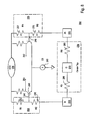
- Input structure 200 includes two input signal pins, pin 205 and pin 210 , for coupling a differential input signal.
- pin 210 will be referred to as receiving a positive, or non-inverted input signal, while pin 205 receives a negative, or inverted, input signal.
- Voltage dividers 220 and 225 are coupled between an input signal node and a power supply or other reference voltage, such as V CC 228 .
- resistors 232 and 237 have a value of 1.5 k ⁇ while resistors 230 and 235 have a value of 1 k ⁇ .
- Intermediate nodes 240 and 245 of voltage divider 220 and 225 are coupled to a first input stage, here a differential pair. In FIG. 8 , voltage at intermediate nodes 240 and 245 will be higher than the input signal coupled to pins 205 and 210 , and lower than reference voltage V CC .
- Resistance values 230 , 232 , 235 , and 237 are chosen such that voltages at node 240 and 245 are large enough to switch input transistors 250 and 255 , yet small enough to not substantially affect operation of current source 260 .
- the impedance values noted above are exemplary, and other values could be used.
- current source 260 can be realized with a wide variety of components and topologies including, but not limited to, the use of bipolar transistors, MOSFETs, and the like. Further, while FIG. 8 depicts an embodiment having input pair bipolar transistors 250 and 255 , other devices including MOSFETs may be used. Further, other input divider topologies may be coupled to nodes 240 and 245 .
- FIG. 8 depicts voltage dividers 220 and 225 coupled between an input signal and a reference signal to support low voltage input signals, where voltage provided at intermediate node 240 is higher than the voltage at input pin 210 .
- voltage dividers may be coupled between an input signal and a reference signal to support high voltage input signals, that is, where a voltage provided at an intermediate node of the voltage divider is lower than the voltage at an input node.
- termination resistor pair 270 comprising center tap 275 is further coupled to input pins 210 and 205 .
- Resistors 280 and 285 are selected to provide a particular termination value, preferably about 50 ohms, and center tap 275 allows for an external connection to accommodate different termination requirements.
- Output to another circuit or device may be taken, for example from nodes 251 and 252 .
- input structures provided by the present invention comprise preferably three nodes, coupleable to external signals or devices.
- those three nodes are input pins 210 and 205 and center tap 275 .
- this three-pin approach is more convenient than a 4-pin approach commonly used.
- the external termination configuration shown in FIG. 1 may be implemented using input structure 200 of FIG. 8 by coupling center tap 275 to voltage V CC .
- the external termination configuration shown in FIG. 2 may be implemented using input structure 200 of FIG. 8 by leaving center tap 275 unconnected, or open.
- the external termination configuration shown in FIG. 3 may be implemented using input structure 200 of FIG. 8 by coupling center tap 275 to voltage (V CC ⁇ 2V).
- the external termination configuration shown in FIGS. 4 and 5 may be implemented using input structure 200 of FIG. 8 , by leaving center tap 275 unconnected, or open.
- the termination configuration shown in FIG. 6 may be implemented using input structure 200 of FIG. 8 by coupling center tap 275 to a ground node.
- Input structures provided by the present invention find use in combination with a variety of circuit topologies and devices.
- Output taken from a first input stage such as from the collector nodes of transistors 250 and 255 in the embodiment shown in FIG. 8 may be coupled to substantially any circuit topology that accepts a differential input, e.g., buffer circuits, switches, amplifiers, and the like.
- FIGS. 9-14 depict possible interfaces between receiving units comprising the above-described three-pin internal termination configuration and transmitting units generating signals according to any of a variety of logic protocols.
- Transmitting, or driver units may be AC-or DC-coupled to a receiving unit comprising a universal input structure.
- some embodiments of the present invention include a V REF — AC pin that allows a simple bias voltage (preferably V CC ⁇ 1.4V) that is also matched to the input stage to be supplied to the center tap pin.
- the V REF — AC pin is not connected or not present.
- FIG. 9 depicts an embodiment of input unit 200 having an interface with CML transmitting unit 300 , where the units are DC-coupled.
- CML transmitting unit 300 is coupled between nodes V CC and ground. Output nodes of CML unit 300 are coupled to pins 210 and 205 of input unit 200 , and center tap pin 275 is not connected, or open.
- Unit 200 further comprises a V REF — AC pin, pin 310 , which is not connected (open) in the embodiment shown in FIG. 9 . In other embodiments, V REF — AC pin 310 is not present.
- FIG. 10 depicts an embodiment of input unit 200 having an interface with CML transmitting unit 315 , where the units are AC-coupled. Capacitors 317 and 319 are each coupled between an output node of unit 315 and an input pin of unit 200 . In this embodiment, center tap 275 is coupled to node V REF — AC 310 .
- FIG. 11 depicts an embodiment of input unit 200 DC-coupled to transmitting unit 320 generating a PECL signal.
- input pins 210 and 205 of unit 200 are coupled to output nodes of transmitting unit 320 .
- Center tap 275 is coupled to a voltage (V CC ⁇ 2V) and pin V REF — AC is not connected, and in some embodiments may not be present.
- FIG. 12 depicts an embodiment of input unit 200 AC-coupled to transmitting unit 325 , generating a PECL signal.
- input pins 210 and 205 of unit 200 are coupled through capacitors 326 and 327 , respectively, to output nodes of transmitting unit 325 .
- Resistors R pd 328 and 329 are further coupled between ground and input pins 210 and 205 , respectively.
- V CC is 3.3 volts and R pd is 220 ⁇ .
- V CC is 2.5V and R pd is 100 ⁇ .
- Center tap 275 is coupled to V REF — AC 310 .
- FIG. 13 depicts an embodiment of input unit 200 DC-coupled to transmitting unit 330 , which generates an LVDS signal.
- Input pins 210 and 205 are coupled to output nodes of LVDS unit 330 .
- Center tap 275 and pin 310 are open, or unconnected. In other embodiments, pin 310 is not provided.
- FIG. 14 depicts an embodiment of input unit 200 DC-coupled to transmitting unit 335 , which generates an HSTL signal.
- Input pins 210 and 205 are coupled to output nodes of HSTL unit 335 .
- Center tap 275 is coupled to a ground node, and V REF — AC pin 310 is not connected, and in some embodiments is not present.
- circuit topologies were coupled between a single V CC power supply and ground.
- embodiments of the present invention include circuit topologies coupled between ground a negative V SS power supply, between two power supplies, V CC and V SS , etc.
- components of the present invention may be fully integrated with one another, or may merely be in functional communication with on another.
- Some or all components described above may be integrated on one or more semiconductor chips, for example, and other components bonded or otherwise brought into communication with the chip or chips. Further, some or all components described above may be packaged and integrated with methods known in the art, for example on printed circuit boards and the like.
- voltage dividers 220 and 225 have been described in terms of two resistors each, voltage dividers 220 and 225 may comprise substantially any components, including resistors, transistors, capacitors, and inductors, such that an intermediate node of the voltage divider is coupled to an input stage in such a way that a voltage at the intermediate node is an appropriate voltage for coupling to the input stage.
Abstract
Description
Claims (37)
Priority Applications (1)
| Application Number | Priority Date | Filing Date | Title |
|---|---|---|---|
| US11/706,833 USRE44134E1 (en) | 2002-09-30 | 2007-02-13 | Universal input apparatus |
Applications Claiming Priority (2)
| Application Number | Priority Date | Filing Date | Title |
|---|---|---|---|
| US10/261,400 US6864707B2 (en) | 2002-09-30 | 2002-09-30 | Universal input apparatus |
| US11/706,833 USRE44134E1 (en) | 2002-09-30 | 2007-02-13 | Universal input apparatus |
Related Parent Applications (1)
| Application Number | Title | Priority Date | Filing Date |
|---|---|---|---|
| US10/261,400 Reissue US6864707B2 (en) | 2002-09-30 | 2002-09-30 | Universal input apparatus |
Publications (1)
| Publication Number | Publication Date |
|---|---|
| USRE44134E1 true USRE44134E1 (en) | 2013-04-09 |
Family
ID=32029983
Family Applications (2)
| Application Number | Title | Priority Date | Filing Date |
|---|---|---|---|
| US10/261,400 Ceased US6864707B2 (en) | 2002-09-30 | 2002-09-30 | Universal input apparatus |
| US11/706,833 Expired - Lifetime USRE44134E1 (en) | 2002-09-30 | 2007-02-13 | Universal input apparatus |
Family Applications Before (1)
| Application Number | Title | Priority Date | Filing Date |
|---|---|---|---|
| US10/261,400 Ceased US6864707B2 (en) | 2002-09-30 | 2002-09-30 | Universal input apparatus |
Country Status (1)
| Country | Link |
|---|---|
| US (2) | US6864707B2 (en) |
Families Citing this family (3)
| Publication number | Priority date | Publication date | Assignee | Title |
|---|---|---|---|---|
| JP2005096094A (en) * | 2003-09-22 | 2005-04-14 | Ricoh Co Ltd | Color image forming apparatus, semiconductor laser modulation driving apparatus and image forming apparatus |
| US7383373B1 (en) * | 2006-03-21 | 2008-06-03 | Emc Corporation | Deriving corresponding signals |
| US7633311B2 (en) * | 2008-01-08 | 2009-12-15 | National Semiconductor Corporation | PECL/LVPECL input buffer that employs positive feedback to provide input hysteresis, symmetric headroom, and high noise immunity |
Citations (5)
| Publication number | Priority date | Publication date | Assignee | Title |
|---|---|---|---|---|
| US6037798A (en) * | 1996-05-08 | 2000-03-14 | Telefonaktiebolaget Lm Ericsson | Line receiver circuit having termination impedances with transmission gates connected in parallel |
| US6292028B1 (en) * | 1998-08-25 | 2001-09-18 | Takashi Tomita | Output circuit for a transmission system |
| US6316964B1 (en) * | 1998-12-08 | 2001-11-13 | Nec Corporation | Method for generating differential tri-states and differential tri-state circuit |
| US6362644B1 (en) * | 2000-08-01 | 2002-03-26 | Semiconductor Components Industries Llc | Programmable termination for integrated circuits |
| US6603329B1 (en) * | 2001-08-29 | 2003-08-05 | Altera Corporation | Systems and methods for on-chip impedance termination |
-
2002
- 2002-09-30 US US10/261,400 patent/US6864707B2/en not_active Ceased
-
2007
- 2007-02-13 US US11/706,833 patent/USRE44134E1/en not_active Expired - Lifetime
Patent Citations (5)
| Publication number | Priority date | Publication date | Assignee | Title |
|---|---|---|---|---|
| US6037798A (en) * | 1996-05-08 | 2000-03-14 | Telefonaktiebolaget Lm Ericsson | Line receiver circuit having termination impedances with transmission gates connected in parallel |
| US6292028B1 (en) * | 1998-08-25 | 2001-09-18 | Takashi Tomita | Output circuit for a transmission system |
| US6316964B1 (en) * | 1998-12-08 | 2001-11-13 | Nec Corporation | Method for generating differential tri-states and differential tri-state circuit |
| US6362644B1 (en) * | 2000-08-01 | 2002-03-26 | Semiconductor Components Industries Llc | Programmable termination for integrated circuits |
| US6603329B1 (en) * | 2001-08-29 | 2003-08-05 | Altera Corporation | Systems and methods for on-chip impedance termination |
Non-Patent Citations (1)
| Title |
|---|
| 3.2.7 Receiver Input Impedance, IEEE Std 1596.3-1996 (IEEE Standard for Low-Voltage Differential Signals (LVDS) for Scalable Coherent Interface (SCI), IEEE Computer Society, Jul. 31, 1996). |
Also Published As
| Publication number | Publication date |
|---|---|
| US20040061520A1 (en) | 2004-04-01 |
| US6864707B2 (en) | 2005-03-08 |
Similar Documents
| Publication | Publication Date | Title |
|---|---|---|
| US4527079A (en) | Integrated circuit device accepting inputs and providing outputs at the levels of different logic families | |
| US7417460B2 (en) | Multi-standard transmitter | |
| US6985009B2 (en) | Signal transmitting system | |
| US20090039916A1 (en) | Systems and Apparatus for Providing a Multi-Mode Memory Interface | |
| JPH03171849A (en) | Signal transmission system and circuit | |
| JPH07264042A (en) | High speed interface circuit | |
| JPH07297678A (en) | Cmos termination resistance circuit | |
| US9467310B2 (en) | Wide common-mode range receiver | |
| US7176709B2 (en) | Receiving device | |
| JPH07235952A (en) | Signal transmission circuit and signal transmission equipment using the same | |
| US6081133A (en) | Universal receiver device | |
| CA2227890A1 (en) | Universal sender device | |
| USRE44134E1 (en) | Universal input apparatus | |
| US6459323B2 (en) | Interface isolator and method for communication of differential digital signals | |
| US6462852B1 (en) | Selectable low-voltage differential signal/current mode logic (LVDS/CML) receiver with the option of AC or DC coupling | |
| JPH0865344A (en) | Backplane bus for differential signal | |
| US6944239B2 (en) | CMOS receiver for simultaneous bi-directional links | |
| JPH0379121A (en) | Semiconductor integrated circuit device | |
| US6850091B2 (en) | Bi-directional impedance matching circuit | |
| US20060119380A1 (en) | Integrated circuit input/output signal termination with reduced power dissipation | |
| US20040161042A1 (en) | Signal transmitting receiving apparatus | |
| US8456189B2 (en) | Differential signal termination circuit | |
| JP3599274B2 (en) | Transimpedance amplifier | |
| EP0811287B1 (en) | Interface isolator circuit for differential signals | |
| KR20020064666A (en) | Driver circuit and data communication device |
Legal Events
| Date | Code | Title | Description |
|---|---|---|---|
| FPAY | Fee payment |
Year of fee payment: 12 |
|
| AS | Assignment |
Owner name: JPMORGAN CHASE BANK, N.A., AS ADMINISTRATIVE AGENT, DELAWARE Free format text: SECURITY INTEREST;ASSIGNORS:MICROCHIP TECHNOLOGY INC.;SILICON STORAGE TECHNOLOGY, INC.;ATMEL CORPORATION;AND OTHERS;REEL/FRAME:053311/0305 Effective date: 20200327 |
|
| AS | Assignment |
Owner name: MICROCHIP TECHNOLOGY INC., ARIZONA Free format text: RELEASE BY SECURED PARTY;ASSIGNOR:JPMORGAN CHASE BANK, N.A, AS ADMINISTRATIVE AGENT;REEL/FRAME:053466/0011 Effective date: 20200529 Owner name: MICROSEMI STORAGE SOLUTIONS, INC., ARIZONA Free format text: RELEASE BY SECURED PARTY;ASSIGNOR:JPMORGAN CHASE BANK, N.A, AS ADMINISTRATIVE AGENT;REEL/FRAME:053466/0011 Effective date: 20200529 Owner name: MICROSEMI CORPORATION, CALIFORNIA Free format text: RELEASE BY SECURED PARTY;ASSIGNOR:JPMORGAN CHASE BANK, N.A, AS ADMINISTRATIVE AGENT;REEL/FRAME:053466/0011 Effective date: 20200529 Owner name: SILICON STORAGE TECHNOLOGY, INC., ARIZONA Free format text: RELEASE BY SECURED PARTY;ASSIGNOR:JPMORGAN CHASE BANK, N.A, AS ADMINISTRATIVE AGENT;REEL/FRAME:053466/0011 Effective date: 20200529 Owner name: ATMEL CORPORATION, ARIZONA Free format text: RELEASE BY SECURED PARTY;ASSIGNOR:JPMORGAN CHASE BANK, N.A, AS ADMINISTRATIVE AGENT;REEL/FRAME:053466/0011 Effective date: 20200529 |
|
| AS | Assignment |
Owner name: WELLS FARGO BANK, NATIONAL ASSOCIATION, MINNESOTA Free format text: SECURITY INTEREST;ASSIGNORS:MICROCHIP TECHNOLOGY INC.;SILICON STORAGE TECHNOLOGY, INC.;ATMEL CORPORATION;AND OTHERS;REEL/FRAME:053468/0705 Effective date: 20200529 |
|
| AS | Assignment |
Owner name: WELLS FARGO BANK, NATIONAL ASSOCIATION, AS COLLATERAL AGENT, MINNESOTA Free format text: SECURITY INTEREST;ASSIGNORS:MICROCHIP TECHNOLOGY INCORPORATED;SILICON STORAGE TECHNOLOGY, INC.;ATMEL CORPORATION;AND OTHERS;REEL/FRAME:055671/0612 Effective date: 20201217 |
|
| AS | Assignment |
Owner name: WELLS FARGO BANK, NATIONAL ASSOCIATION, AS NOTES COLLATERAL AGENT, MINNESOTA Free format text: SECURITY INTEREST;ASSIGNORS:MICROCHIP TECHNOLOGY INCORPORATED;SILICON STORAGE TECHNOLOGY, INC.;ATMEL CORPORATION;AND OTHERS;REEL/FRAME:057935/0474 Effective date: 20210528 |
|
| AS | Assignment |
Owner name: MICROSEMI STORAGE SOLUTIONS, INC., ARIZONA Free format text: RELEASE BY SECURED PARTY;ASSIGNOR:WELLS FARGO BANK, NATIONAL ASSOCIATION, AS NOTES COLLATERAL AGENT;REEL/FRAME:059863/0400 Effective date: 20220228 Owner name: MICROSEMI CORPORATION, ARIZONA Free format text: RELEASE BY SECURED PARTY;ASSIGNOR:WELLS FARGO BANK, NATIONAL ASSOCIATION, AS NOTES COLLATERAL AGENT;REEL/FRAME:059863/0400 Effective date: 20220228 Owner name: ATMEL CORPORATION, ARIZONA Free format text: RELEASE BY SECURED PARTY;ASSIGNOR:WELLS FARGO BANK, NATIONAL ASSOCIATION, AS NOTES COLLATERAL AGENT;REEL/FRAME:059863/0400 Effective date: 20220228 Owner name: SILICON STORAGE TECHNOLOGY, INC., ARIZONA Free format text: RELEASE BY SECURED PARTY;ASSIGNOR:WELLS FARGO BANK, NATIONAL ASSOCIATION, AS NOTES COLLATERAL AGENT;REEL/FRAME:059863/0400 Effective date: 20220228 Owner name: MICROCHIP TECHNOLOGY INCORPORATED, ARIZONA Free format text: RELEASE BY SECURED PARTY;ASSIGNOR:WELLS FARGO BANK, NATIONAL ASSOCIATION, AS NOTES COLLATERAL AGENT;REEL/FRAME:059863/0400 Effective date: 20220228 |
|
| AS | Assignment |
Owner name: MICROSEMI STORAGE SOLUTIONS, INC., ARIZONA Free format text: RELEASE BY SECURED PARTY;ASSIGNOR:WELLS FARGO BANK, NATIONAL ASSOCIATION, AS NOTES COLLATERAL AGENT;REEL/FRAME:059363/0001 Effective date: 20220228 Owner name: MICROSEMI CORPORATION, ARIZONA Free format text: RELEASE BY SECURED PARTY;ASSIGNOR:WELLS FARGO BANK, NATIONAL ASSOCIATION, AS NOTES COLLATERAL AGENT;REEL/FRAME:059363/0001 Effective date: 20220228 Owner name: ATMEL CORPORATION, ARIZONA Free format text: RELEASE BY SECURED PARTY;ASSIGNOR:WELLS FARGO BANK, NATIONAL ASSOCIATION, AS NOTES COLLATERAL AGENT;REEL/FRAME:059363/0001 Effective date: 20220228 Owner name: SILICON STORAGE TECHNOLOGY, INC., ARIZONA Free format text: RELEASE BY SECURED PARTY;ASSIGNOR:WELLS FARGO BANK, NATIONAL ASSOCIATION, AS NOTES COLLATERAL AGENT;REEL/FRAME:059363/0001 Effective date: 20220228 Owner name: MICROCHIP TECHNOLOGY INCORPORATED, ARIZONA Free format text: RELEASE BY SECURED PARTY;ASSIGNOR:WELLS FARGO BANK, NATIONAL ASSOCIATION, AS NOTES COLLATERAL AGENT;REEL/FRAME:059363/0001 Effective date: 20220228 |
|
| AS | Assignment |
Owner name: MICROSEMI STORAGE SOLUTIONS, INC., ARIZONA Free format text: RELEASE BY SECURED PARTY;ASSIGNOR:WELLS FARGO BANK, NATIONAL ASSOCIATION, AS NOTES COLLATERAL AGENT;REEL/FRAME:060894/0437 Effective date: 20220228 Owner name: MICROSEMI CORPORATION, ARIZONA Free format text: RELEASE BY SECURED PARTY;ASSIGNOR:WELLS FARGO BANK, NATIONAL ASSOCIATION, AS NOTES COLLATERAL AGENT;REEL/FRAME:060894/0437 Effective date: 20220228 Owner name: ATMEL CORPORATION, ARIZONA Free format text: RELEASE BY SECURED PARTY;ASSIGNOR:WELLS FARGO BANK, NATIONAL ASSOCIATION, AS NOTES COLLATERAL AGENT;REEL/FRAME:060894/0437 Effective date: 20220228 Owner name: SILICON STORAGE TECHNOLOGY, INC., ARIZONA Free format text: RELEASE BY SECURED PARTY;ASSIGNOR:WELLS FARGO BANK, NATIONAL ASSOCIATION, AS NOTES COLLATERAL AGENT;REEL/FRAME:060894/0437 Effective date: 20220228 Owner name: MICROCHIP TECHNOLOGY INCORPORATED, ARIZONA Free format text: RELEASE BY SECURED PARTY;ASSIGNOR:WELLS FARGO BANK, NATIONAL ASSOCIATION, AS NOTES COLLATERAL AGENT;REEL/FRAME:060894/0437 Effective date: 20220228 |