WO1998009400A1 - Receiving and equalizing signals for high-speed data transmission - Google Patents
Receiving and equalizing signals for high-speed data transmission Download PDFInfo
- Publication number
- WO1998009400A1 WO1998009400A1 PCT/IB1996/000873 IB9600873W WO9809400A1 WO 1998009400 A1 WO1998009400 A1 WO 1998009400A1 IB 9600873 W IB9600873 W IB 9600873W WO 9809400 A1 WO9809400 A1 WO 9809400A1
- Authority
- WO
- WIPO (PCT)
- Prior art keywords
- filter
- estimate
- analog
- value
- time
- Prior art date
Links
Classifications
-
- H—ELECTRICITY
- H04—ELECTRIC COMMUNICATION TECHNIQUE
- H04L—TRANSMISSION OF DIGITAL INFORMATION, e.g. TELEGRAPHIC COMMUNICATION
- H04L7/00—Arrangements for synchronising receiver with transmitter
- H04L7/0054—Detection of the synchronisation error by features other than the received signal transition
- H04L7/0062—Detection of the synchronisation error by features other than the received signal transition detection of error based on data decision error, e.g. Mueller type detection
-
- H—ELECTRICITY
- H04—ELECTRIC COMMUNICATION TECHNIQUE
- H04L—TRANSMISSION OF DIGITAL INFORMATION, e.g. TELEGRAPHIC COMMUNICATION
- H04L25/00—Baseband systems
- H04L25/02—Details ; arrangements for supplying electrical power along data transmission lines
- H04L25/03—Shaping networks in transmitter or receiver, e.g. adaptive shaping networks
- H04L25/03006—Arrangements for removing intersymbol interference
- H04L25/03178—Arrangements involving sequence estimation techniques
- H04L25/03203—Trellis search techniques
- H04L25/03235—Trellis search techniques with state-reduction using feedback filtering
Definitions
- This invention relates to transceivers for high-speed, i.e. several Mbit-per-second, data transmission over unshielded twisted-pair cables or other transmission means with similar transfer characteristics. It specifically provides a solution for a low- power transceiver in such systems.
- One implementation employs quaternary partial-response class-IV (PRIV) signaling in combination with new concepts for mixed adaptive analog and digital equalization, clock recovery, and Viterbi decoding.
- Another implementation is for full-response systems.
- Unshielded twisted-pair (UTP) cables are a preferred transmission medium for many applications that require transmission of data at the speed of several Mbit/sec, in particular for local area networks (LANs).
- Data transmission systems with UTP cables are also employed to provide high speed connectivity to subscribers over the copper access network, e.g. by high speed digital subscriber lines (HDSLs) or asymmetric digital subscriber lines (ADSLs).
- HDSLs high speed digital subscriber lines
- ADSLs asymmetric digital subscriber lines
- Other applications can be found in networks deployed to collect measurement data, e.g. for seismic data acquisition.
- the sample x can be expressed in general as the weighted sum
- N -1 representing the sampled overall system response and w n denoting additive noise.
- Higher spectral efficiency than in binary transmission is obtained by M- ary multi-level transmission, where the symbol set is
- intersymbol interference is introduced in a controlled fashion to shape the overall channel response.
- partial- response class-IV defined by the system polynomial 1-D 2
- PRIV partial- response class-IV
- Signal shaping functions at the receiver usually include variable gain amplification and fixed and adaptive equalization.
- Signal samples are obtained by analog-to-digital (A/D) conversion of the signal at the analog front-end output at sampling instants that are determined by a timing recovery circuit.
- A/D analog-to-digital
- a sampling rate larger than 1/Tsamples/s may be required to avoid aliasing.
- a sequence of signals at a rate of 1/Tsamples/s is obtained at the output of a digital filter that performs the functions of equalization and decimation.
- Adaptive equalization can be performed either in the analog domain by variable analog filters or in the digital domain, e.g. by adaptive linear transversal filters.
- a well-known technique for adaptive analog equalization is the automatic line build-out (ALBO) technique.
- An ALBO equalizer can be described as a combination of a variable-length cable simulator and an appropriate fixed receive filter. Since, for transmission over metallic cables, signal distortion depends essentially on one quantity, i.e. the product of a cable parameter times the cable length, a single control parameter is traditionally adjusted such that a given output signal level is obtained. The combined lengths of the cable and the simulated cable add then up to a known cable length for which the overall channel is equalized.
- ALBO-type equalizers are described in: "Transmission Systems for Communication", Bell Telephone Laboratories, Fourth Edition 1970, pp. 654-655, and in US Patent 5455 843 to Cherubini et al., entitled “Adaptive Equalizing Appa- ratus and Method for Token Ring Transmission System Using Unshielded Twisted Pair Cables".
- the patent discloses an analog equalizer and an associated method to adaptively adjust the equalizer transfer characteristic for a distance between stations that can typically extend up to 200 m. For this range, the attenuation of unshielded twisted pair (UTP) cables is about 10 - 12 dB/100 m at 16 MHz so that the channel attenuation at 16 MHz varies between 0 and 24 dB.
- an ALBO-type equalizer can be realized as a single monolithic semiconductor chip, such as the serial data receiver LIU-01 by Precision Monolithics Inc.
- an ALBO-type equalizer cannot adequately compensate for the signal distortion if large deviations from the assumed values occur In this case, signal equalization can be performed - either partially or entirely - by digital filtering.
- a tutorial treatise on adaptive digital equalization can be found in E A Lee and D. G. Messerschmitt: "Digital Communication", Kluwer Academic Publishers, Boston, MASS, USA, 1988, Ch. 9.
- a digital decision-feedback equalizer consists of a linear forward digital filter and a feedback digital filter where past decisions are employed to compute the filter out- put.
- Initial convergence of the DFE coefficients to their optimum values is traditionally achieved by reference-directed training where a symbol sequence known to the receiver is sent prior to transmitting the data.
- initial DFE convergence must be achieved in a self-training mode
- Self-training adaptive linear equalization for full-response systems was described, e.g., by D.N. Godard in "Self-recovering equalization and carrier tracking in two-dimensional data communication systems", IEEE Trans. Commun., Vol. COM-28, pp.
- the feedback filter of a DFE can be embedded in a Viterbi decoder, as described by A. Duel-Hallen and C. Heegard in "Delayed decision-feedback equalization", IEEE Trans. Commun., Vol. COM-37, pp. 428-436, May 1989, and by M.V. Eyuboglu and S.U. Qureshi in "Reduced-state sequence estimation for coded modulation on intersymbol interference channel", IEEE Trans. 20 Commun., Vol. COM-37, pp. 989 -995, Aug. 1989.
- Viterbi decoder for partial-response signals was described by S. Oelcer and G. Ungerboeck in "Difference-metric Viterbi decoding of multilevel class-IV partial-response signals", IEEE Trans. Commun., Vol. COM-42, pp. 1558 -1570, Apr. 1994.
- Timing synchronization is usually accomplished by decision-aided schemes.
- a decision-directed timing recovery scheme that can be applied to full- and partial-response systems was described by K. H. Mueller and M. Muller in "Timing recovery in digital synchronous data receivers", IEEE Trans. Commun., Vol. COM-24, pp. 516-531 , Sept. 1976.
- K. H. Mueller and M. Muller in "Timing recovery in digital synchronous data receivers", IEEE Trans. Commun., Vol. COM-24, pp. 516-531 , Sept. 1976.
- undesirable false-lock situations can be experienced during initial timing acquisition.
- transceiver power consumption is not subject to particularly tight constraints.
- transceivers employed in adapter cards installed in personal computers or the like have usually sufficient power available.
- power is a scarce resource, which imposes that the employed transceivers operate with minimal power consumption. This is the case, for example, for LANs deployed outside of buildings where the various devices connected to the network are battery-operated. Under such conditions, precise power management is required.
- a further object is to devise a method and a receiver providing robustness against various channel impairments and be tolerant of inaccuracies present particularly in the analog receiver sections.
- Another object is to devise methods and apparatus to allow a receiver in a full-response or a partial-response system to be able to acquire initial convergence of its parameters for timing recovery and decision-feedback equalization using received random data signals only, i.e. without the need for a reference-directed start-up procedure.
- DFE decision-feedback equalizer
- the solution to these objects consists in employing, in the receiver, a novel timing recovery scheme, preferably in connection with novel approaches for self-training decision-feedback equalization to be applied to full or partial-response transmission systems. Details of these solutions are given in the appended detailed description of a first implementation of the invention in a four-level PRIV system for data transmission over UTP cables, and in a second implementation in a full-response system.
- the principles and concepts of the disclosed receiving techniques are not limited to data transmission over UTP cables but can as well be applied, with appropriate modifications obvious to a person skilled in the art, for data transmission over other types of channels, e.g., magnetic recording channels.
- the invention addresses two different issues. First, it solves the problem of timing recovery.
- the solution according to the invention for a quaternary PRIV system shows the linear forward equalizer realized as a self-training two-parameter variable analog filter.
- Two-parameter variable equalizer adjustment for partial-response systems goes back to the theoretical principle explained by Cherubini and Ungerboeck in "Equalizer, Gain, and Timing Control in a Receiver for Multilevel Partial-Response Signals", cited above.
- the linear forward equalization by a variable analog filter leads to the advantage of low power consumption. After synchronization has been accomplished, convergence of the digital feedback filter embedded in a reduced- state Viterbi decoder is achieved. This approach leads to an implementation with low complexity that permits to reduce power consumption even further.
- the small adaptivity provided by the Viterbi decoder allows compensating for the residual signal distortion at the output of the analog linear forward equalizer and ensures correct convergence of the feedback filter coefficients to their optimum values without the need for a training sequence.
- the solution according to the invention for a full-response system shows the linear forward equalizer realized as a self-training adaptive digital filter.
- the algorithm employed for self-training equalization is an inventive extension to full-response systems of the algorithm for partial-response systems described by Cherubini, Oelcer, and Ungerboeck in "Adaptive equalization for PRIV transmission systems", cited above.
- convergence of the feedback filter coefficients to their optimum values takes place without the need for a training sequence after timing recovery and convergence of the linear forward equalizer have been accomplished.
- F ⁇ g.1 shows an overview of the system in which the invention is used;
- F ⁇ g.2 illustrates a connection between two nodes in the system according to Fig.1 ;
- Fig.3 depicts a first embodiment, a transceiver in a partial-response system;
- Fig.4 illustrates the computation of the timing control signal;
- Fig.5 shows a second embodiment, a transceiver in a full-response system.
- Fig.1 provides a simplified overview of a system which makes advantageous use of the invention, a system developed for seismic data acquisition.
- a backbone network connects router units (RUs) 2 via bi-directional high-speed fiber links 3 to a central system 1.
- Ground networks connect signal processing units (SPUs) 6 via bidirectional cable links 4 to the RUs.
- SPU 6 can receive analog signals from a plurality of geophones 7, digitize these signals, and send them upstream to central system 1.
- each SPU 6 receives and transmits control and status information.
- Fig.2 illustrates the communication arrangement between two adjacent SPUs 6.
- the SPU functions are controlled by a controller 8 which interfaces with two transceivers 9 designated T1 and T2.
- each transceiver 9 supports full-duplex transmission at a nominal rate of 16 Mbit/s, and at a fallback rate of 8 Mbit/s.
- the cable links 4 connecting two SPUs contain unshielded twisted-pair ca- bles 11 for digital transmission, and additional pairs 10 over which analog signals from geophones 7 (shown in Fig.1 ) are received and digitized by converter 5. Power consumption for simultaneous transmit and receive operation is less than 200 mW from a single 3.3V supply voltage.
- the characteristics of the cables used for the cable links 4 are specified as follows: - 30 dB signal attenuation at 4 MHz for maximum cable length,
- the two transceivers 9 shown schematically in Fig.2 are controlled via a common microcontroller which permits setting of transceiver options, e.g. quaternary trans- mission or binary transmission (as a fallback), and reading of receiver parameters, e.g. mean squared-error at the detection point of each receiver.
- transceiver options e.g. quaternary trans- mission or binary transmission (as a fallback)
- receiver parameters e.g. mean squared-error at the detection point of each receiver.
- the transceiver design is based on quaternary partial-response class-IV (QPRIV) signaling.
- the overall channel characteristic exhibits spectral nulls at 0 Hz and the bandedge frequencies of ⁇ 1/2 THz, where 1/7 ' , here 8 MBaud, is the modulation rate.
- transmitted signal energy is greatly reduced at low frequencies, where the transfer function of the cable varies rapidly with frequency, and at high frequencies, where signals become more attenuated.
- Channel equalization can thus be accomplished more easily than for full-response signaling and partial-response class-l signaling (PRI) with spectral nulls only at ⁇ 1/27
- Fig.3 gives an overview of one single transceiver incorporating the invention.
- Each transceiver consists of a digital section 12 in which digital signal processing functions are performed, and a front-end section 13 for signal conversion, analog filtering, receiver clock generation, and cable driver/receiver functions.
- incoming quaternary symbols are represented by a 2-bit signal TDAT.
- These incoming information bits are scrambled in self-synchronizing scrambler 14 using the scrambler polynomial ⁇ + D 13 + D 28 and encoded by a 2B1Q differential encoder 15 to achieve transparency with respect to received signal polarity.
- the resulting signal is shaped by a fixed transmit filter 17 into approximate PRIV form, then amplified by power amplifier 18, and transmitted via cable 11.
- An incoming signal - from cable 11 - is amplified by variable gain amplifier (VGA) 19 and shaped into PRIV form by an analog receive filter consisting of a variable filter section 20 and a fixed filter section 21.
- VGA variable gain amplifier
- variable equalizer Two independent control voltages determine the adjustments carried out by the variable equalizer: one voltage determines the frequency-independent gain of VGA 19, the other voltage controls the transfer characteristic of variable filter 20.
- the control signals for the variable equalizer are derived digitally in a manner that leads to optimum settings independently of the current sampling phase.
- Received signal samples x n are obtained in analog-to-digital (A/D) converter 22 by 6-bit A/D conversion at a rate equal to MT symbols per second.
- the sampling phase of A/D converter 22 is determined by a voltage-controlled oscillator (VCO) 23 whose control voltage is adjusted by a decision-directed timing recovery algorithm. For proper operation of the timing recovery algorithm, a sufficient degree of equalization has to be achieved by the sampling-phase insensitive equalizer control method.
- the control voltage for VCO 23 is provided by control circuit 29 in binary sigma-delta modulated form, as are the control voltages for VGA 19 and the variable filter section 20.
- a bank of three sigma-delta demodulators 24 to 26 serves to derive the required analog control voltages.
- the thus obtained 6-bit-wide digital signal samples are input to an adaptive reduced two-state Viterbi decoder, element 27, for maximum-likelihood sequence detection.
- element 27 Embedded in this Viterbi decoder is the adaptive feedback filter of a decision- feedback equalizer (DFE) to remove residual intersymbol interference. Symbol-by- symbol detection can also be employed.
- element 27 consists of a memory-less decision element and a feedback filter.
- MSE average squared error signal
- the MSE and other digital section receiver parameters may be used to allow monitoring of a "transmission-link quality".
- the signals at the output of the Viterbi decoder are differentially decoded and descrambled in descrambler 30.
- the recovered quaternary symbols are represented by the two-bit signal RDAT at the output of the digital section 12 of the transceiver.
- Light line 31 in F ⁇ g.3 carries a receiver clock signal RCLK produced by VCO 23; this clock signal RCLK controls all digital receiver functions.
- an externally provided transmitter clock signal TCLK serves the same function, as indicated.
- the transceiver comprises a digital chip and a mixed analog/digital chip; it further includes various external components, such as analog filters, transformers, oscillator crystal, etc., which are not shown in detail; a person skilled in the art will be able to implement them.
- the digital chip performs the required digital signal processing functions and also incorporates a microcontroller interface.
- the mixed analog/digital chip performs the functions of D/A conversion and power amplification required for the transmit section of the transceiver front-end and the functions of variable gain amplification, signal buffering and A/D conversion needed for the receive section.
- Fixed passive analog filters for signal shaping are realized as a hybrid module.
- Analog signal equalization capability is provided by an external variable filter section.
- the variable elements of the variable filter can be realized, for example, by employing a matched n-channel JFET pair.
- receiver timing is provided by VCO 23, which is here implemented as a voltage- controlled crystal oscillator.
- the main features of the transceiver as implemented for a LAN for seismic data acquisition are:
- control voltage u K ⁇ A determines a frequency-independent gain of amplifier 19
- control voltage u EQZ varies the transfer function of the variable filter section 20
- control voltage U ⁇ Q controls the frequency of the voltage-controlled oscillator 23 and thus the sampling phase t s of A/D converter 22.
- the adjustments for these control voltages are computed in the digital transceiver section 12 by the following algorithms.
- VCA n ( 0 if otherwise.
- VCA n ( 0 if otherwise.
- the value VCA n is then converted into a single-bit control signal by first-order sigma-delta demodulation, not described here.
- U EQZn l U EQl.n " O ⁇ " ⁇ > 0 ⁇ d E « J , wherein ⁇ is an adaptation gain.
- the value u EQZn is then converted into a single-bit control signal by first-order sigma-delta demodulation, not described here.
- the stochastic gradient of E ⁇ (x n - s ⁇ with respect to the sampling phase t s is proportional to (x n - sj x inhabit « (x n - s (x ⁇ +l - x n , wherein xicide is a time derivative of x n . This leads to the definition of the gradient given by Muller and Mueller:
- the received signal denoted by x n
- ⁇ hi represents an estimate of the coefficient ⁇ hi at time n
- the Viterbi decoder operates on the signals ⁇ n ⁇ and determines the symbol sequence ⁇ a amid ⁇ which minimizes
- the estimates of the channel impulse responses ⁇ ⁇ 0> , ⁇ , ⁇ , repet, ⁇ 9, place are deter- mined by an adaptive LMS algorithm such as to minimize ⁇ esammlung .
- reduced-state Viterbi decoding is employed. State reduction is achieved by grouping the two states corresponding to the symbols +3 and -1 into one single state, and by grouping the two states corresponding to the symbols +1 and -3 into a second state. Note that state reduction requires that parallel transitions are resolved prior to the computation of the branch metrics. In order to reduce propagation delay, parallel transitions are resolved using the signal x n rather than x tripod . This approach is justified by our earlier assumption that the channel impulse response does not significantly deviate from the impulse response of an ideal PRIV channel. Note also that since at any time instant only two states are retained, the difference of the survivor metrics can be propagated from one iteration to the next, rather than the survivor metrics themselves.
- a block diagram with the main functions of the adaptive Viterbi decoder with auxiliary feedback filter can be developed by someone skilled in the art.
- the difference metric is iteratively computed, the extension of
- ⁇ ⁇ the survivor sequences is determined, and the estimates ⁇ A 0, adjuvant and ⁇ h l n are obtained by an adaptive LMS algorithm.
- a path history unit is used to store the two survivor sequences.
- An adaptive auxiliary feedback filter computes the signal correction term
- I ⁇ , l ⁇ 2 using tentative symbol decisions stored in the path history unit, and adaptively gen-
- the mean-squared error is computed in MSE meter 28 by low-pass filtering the metric increments.
- the bits representing the symbols output by the Viterbi decoder 27 are differentially decoded and descrambled by descrambler 29 which includes a descrambler whose transfer function is given by (l + D' 3 + D 28 ).
- the descrambler output signal represents the recovered information bits. This concludes the description of the partial- response system.
- Fig.5 An embodiment of the invention for a quaternary full-response system is shown in Fig.5 and described in the following.
- the filtering elements at the transmitter and the receiver must ensure that the signal y n obtained at the decision element of an adaptive digital equalizer 57, in the embodiment a DFE, is free from intersymbol interference.
- DFE is realized by a digital transversal filter.
- Fig.5 gives an overview of a transceiver incorporating a full-response embodiment according to the invention.
- Each transceiver consists of a digital section 42, in which digital signal processing functions are performed, and a front-end section 43 for signal conversion, analog filtering, receiver clock generation, and cable driver/receiver functions.
- incoming quaternary symbols are represented by a 2-bit signal TDAT.
- These incoming information bits are scrambled in scrambler 44 using the polynomial l+ D' 3 + D 28 and encoded by a 2B1Q differential encoder 45 to achieve transparency with respect to received signal polarity.
- the resulting signal is shaped by a fixed transmit filter 47, then amplified by power amplifier 48, and transmitted via cable 41.
- VGA variable gain amplifier
- Received signal samples x n are obtained in analog-to-digital (A/D) converter 52 by 6-bit A/D conversion at a rate of MT symbols per second.
- the sampling phase of A/D converter 52 is determined by a voltage-controlled oscillator (VCO) 53 whose control voltage is adjusted by the disclosed decision-directed timing recovery algo- rithm.
- VCO voltage-controlled oscillator
- the control voltage for VCO 53 is provided by control circuit 59 in binary sigma-delta modulated form, as is the control voltage for VGA 49.
- Two sigma-delta demodulators 54 and 56 serve to derive the required analog control voltages.
- &I iêt - •••• d L ⁇ n ⁇ denotes the vector of coefficients of the feedback filter
- x ⁇ x n x ⁇ ⁇
- +1 ⁇ represents the vector of signals stored in the equalizer delay line at time n
- b ⁇ ⁇ l ⁇ n L+i ⁇ represents the vector of tentative quaternary decisions stored in the feedback filter delay line at time n.
- the generation of the pseudo error J. is based on a priori knowledge of the statistics of the signal.
- y n corresponds to the quaternary channel input symbols a r embedded in noise. Therefore, whenever the event ⁇ y n ⁇ > 3 is observed, we can use y n - ⁇ n as a trusted error to update the equalizer coefficients. If we observe the event y n ⁇ ⁇ 3, no trusted error is available.
- pseudo errors can be computed based on the signal energy at the equalizer output. If the signal energy is found to be too often below a given threshold, the error term is set equal to - c s ⁇ gn(y n ), where c is a positive constant, whenever ⁇ y n ⁇ ⁇ 3 , and trusted errors are used when ⁇ y n ⁇ > 3 .
- symbol-rate sampling at the receiver is assumed .
- the extension of the described self- training algorithm to this case is straightforward.
- MSE average squared error signal
- the signals at the output of the decision feedback filter are differentially decoded and descrambled in descrambler 60.
- the recovered quaternary symbols are represented by the two-bit signal RDAT at the output of the digital section 42 of the transceiver.
- Light line 61 in Fig.5 carries a receiver clock signal RCLK' produced by VCO 53; this clock signal RCLK' controls all digital receiver functions.
- an externally provided transmitter clock signal TCLK' serves the same function, as indicated.
Abstract
Methods and apparatus are disclosed for receiving and/or equalizing data signals transmitted over metallic lines or other means with similar transfer characteristics in communication systems employing multi-level partial-response or full-response signaling. They comprise a novel timing recovery scheme in conjunction with mixed analog/digital or fully digital decision-feedback equalization; this novel scheme avoids false lock situations that can be experienced during initial timing acquisition. Also addressed is the problem of initial convergence of an adaptive decision-feedback equalizer (DFE) in self-training mode. For partial-response systems, the problem is solved by implementing the linear forward filter of the DFE as a two-parameter variable analog filter, for which convergence can be achieved prior to timing recovery. Linear forward equalization by a variable analog filter also leads to the advantage of low power consumption. After initial convergence at the analog filter, decisions obtained at the analog channel output are sufficiently reliable so that timing recovery can be achieved. Then, convergence at the feedback filter of the DFE embedded in an adaptive Viterbi decoder takes place. For full-response systems, fully digital adaptive DFE is used. Timing recovery is accomplished prior to convergence at the linear forward equalizer. Self-training equalization is achieved by a specific method that allows reliable convergence of the coefficients of the DFE to the optimum values.
Description
DESCRIPTION
Receiving and Equalizing Signals for High-Speed Data Transmission
FIELD OF THE INVENTION
This invention relates to transceivers for high-speed, i.e. several Mbit-per-second, data transmission over unshielded twisted-pair cables or other transmission means with similar transfer characteristics. It specifically provides a solution for a low- power transceiver in such systems. One implementation employs quaternary partial-response class-IV (PRIV) signaling in combination with new concepts for mixed adaptive analog and digital equalization, clock recovery, and Viterbi decoding. Another implementation is for full-response systems.
BACKGROUND AND PRIOR ART
Unshielded twisted-pair (UTP) cables are a preferred transmission medium for many applications that require transmission of data at the speed of several Mbit/sec, in particular for local area networks (LANs). Data transmission systems with UTP cables are also employed to provide high speed connectivity to subscribers over the copper access network, e.g. by high speed digital subscriber lines (HDSLs) or asymmetric digital subscriber lines (ADSLs). Other applications can be found in networks deployed to collect measurement data, e.g. for seismic data acquisition.
In a digital transmission system, data can be recovered from the sequence of samples xn taken at the output of the overall channel at instants / = nT+τ , where T s the modulation interval, and τ is a constant sampling phase.
The sample x„can be expressed in general as the weighted sum
Λ/-1 xn =∑ h,a„-, + w„ , ι=0 where a„ e A is the n-ih input symbol taken from the symbol set A, ht , / = 0
N -1 representing the sampled overall system response and wn denoting additive noise. In a binary transmission system, the input symbols are taken from the set A = { -1 , +1}. Higher spectral efficiency than in binary transmission is obtained by M- ary multi-level transmission, where the symbol set is
A = { -(M-1), .... -1, +1, ... (M-1)} with M > 2, M even, A = [ -(M-1), .... -2, 0, +2, ... (M-1)} with M > 2, M odd.
Introducing the Zλtransform notation, the sampled overall response can be expressed by the system polynomial (D) =∑ h,D' , ι=0 wherein D denotes the unit-delay operator.
A full-response system is characterized by the absence of intersymbol interference, i.e. h(D) = 1. In partial-response systems, intersymbol interference is introduced in a controlled fashion to shape the overall channel response. For example, partial- response class-IV (PRIV), defined by the system polynomial 1-D2, is well-suited for DC-free and band-limited transmission over metallic cables because the overall frequency response presents spectral nulls at f = 0 Hz and |f| = 1/2 Hz, where T denotes the modulation interval.
Overall signal shaping to full or partial response is obtained by proper design of the filters in the analog and the digital sections at the transmit and receive ends of the transmission link. Signal shaping functions at the receiver usually include variable gain amplification and fixed and adaptive equalization. Signal samples are obtained by analog-to-digital (A/D) conversion of the signal at the analog front-end output at sampling instants that are determined by a timing recovery circuit. In full-response systems, a sampling rate larger than 1/Tsamples/s may be required to avoid
aliasing. In this case, a sequence of signals at a rate of 1/Tsamples/s is obtained at the output of a digital filter that performs the functions of equalization and decimation.
Signal distortion introduced by homogeneous metallic transmission lines is mainly caused by the skin effect. In a receiver for a cable transmission system, signal distortion is usually compensated for by adaptive equalization. Adaptive equalization can be performed either in the analog domain by variable analog filters or in the digital domain, e.g. by adaptive linear transversal filters. A well-known technique for adaptive analog equalization is the automatic line build-out (ALBO) technique. An ALBO equalizer can be described as a combination of a variable-length cable simulator and an appropriate fixed receive filter. Since, for transmission over metallic cables, signal distortion depends essentially on one quantity, i.e. the product of a cable parameter times the cable length, a single control parameter is traditionally adjusted such that a given output signal level is obtained. The combined lengths of the cable and the simulated cable add then up to a known cable length for which the overall channel is equalized.
Examples of ALBO-type equalizers are described in: "Transmission Systems for Communication", Bell Telephone Laboratories, Fourth Edition 1970, pp. 654-655, and in US Patent 5455 843 to Cherubini et al., entitled "Adaptive Equalizing Appa- ratus and Method for Token Ring Transmission System Using Unshielded Twisted Pair Cables". The patent discloses an analog equalizer and an associated method to adaptively adjust the equalizer transfer characteristic for a distance between stations that can typically extend up to 200 m. For this range, the attenuation of unshielded twisted pair (UTP) cables is about 10 - 12 dB/100 m at 16 MHz so that the channel attenuation at 16 MHz varies between 0 and 24 dB. The disclosed equalization method is limited to a specific application and cabling structure which makes the disclosed solution unsuitable to cope with the objects of the present invention. In present day cable systems, an ALBO-type equalizer can be realized as a single monolithic semiconductor chip, such as the serial data receiver LIU-01 by Precision Monolithics Inc.
In a paper entitled "Equalizer, Gain, and Timing Control in a Receiver for Multi-level Partial-Response Signals", in the Proceedings of the Fifth Tirrenia International Workshop on Digital Communications, Elsevier Science Publishers B.V., 1992, Cherubini and Ungerboeck describe the adjustment of a two-parameter equalizer consisting of a variable analog filter section and a vanable gain amplifier, as well as the adjustment of the sampling phase of an A/D converter in the front-end of a receiver for multi-level PRIV transmission. In the described device, a first control voltage adjusts the variable filter section and a second control voltage determines the front-end gain. The control voltages are derived from the digital output signals of the A/D converter.
The design of a two-parameter equalizer as well as fixed transmit and receive filter sections for PRIV systems was described by G. Cherubini, S. Oelcer, and G. Ungerboeck in "Optimum Filter Design for Partial-Response Class-IV Transmission Systems", Proc. IEEE Intl. Conf. on Communications, ICC '92, pp. 51-56, Chicago, IL, USA, June 1992.
However, an ALBO-type equalizer cannot adequately compensate for the signal distortion if large deviations from the assumed values occur In this case, signal equalization can be performed - either partially or entirely - by digital filtering. A tutorial treatise on adaptive digital equalization can be found in E A Lee and D. G. Messerschmitt: "Digital Communication", Kluwer Academic Publishers, Boston, MASS, USA, 1988, Ch. 9.
For the present invention, decision-feedback equalization is considered. A digital decision-feedback equalizer (DFE) consists of a linear forward digital filter and a feedback digital filter where past decisions are employed to compute the filter out- put. Initial convergence of the DFE coefficients to their optimum values is traditionally achieved by reference-directed training where a symbol sequence known to the receiver is sent prior to transmitting the data. When a training sequence is not available, initial DFE convergence must be achieved in a self-training mode
Self-training adaptive linear equalization for full-response systems was described, e.g., by D.N. Godard in "Self-recovering equalization and carrier tracking in two-dimensional data communication systems", IEEE Trans. Commun., Vol. COM-28, pp. 1867-1875, Nov. 1980, by S. Bellini in "Bussgang techniques for blind 5 equalization", Proc. of IEEE Globecom 1986, pp. 46.1.1 - 46.1.7 , Dec. 1986, and by G. Picchi et al. in "Blind equalization and carrier recovery using a "Stop-and-Go" decision directed algorithm", IEEE Trans. Commun., Vol. COM-35, pp. 877- 887, Sept. 1987. For partial-response systems, self-training adaptive linear equalization was described by Y. Sato in "A method of self-recovering equalization for multilevel 10 amplitude-modulation systems", IEEE Trans. Commun., Vol. COM-23, pp. 679-682, June 1975, and by G. Cherubini, S. Oelcer, and G. Ungerboeck in "Adaptive equalization for PRIV transmission systems", PCT International Patent Application, Publication Number WO 96/20551.
To achieve near maximum-likelihood sequence detection of signals in the presence 15 of intersymbol interference (ISI), the feedback filter of a DFE can be embedded in a Viterbi decoder, as described by A. Duel-Hallen and C. Heegard in "Delayed decision-feedback equalization", IEEE Trans. Commun., Vol. COM-37, pp. 428-436, May 1989, and by M.V. Eyuboglu and S.U. Qureshi in "Reduced-state sequence estimation for coded modulation on intersymbol interference channel", IEEE Trans. 20 Commun., Vol. COM-37, pp. 989 -995, Aug. 1989. The implementation of a Viterbi decoder for partial-response signals was described by S. Oelcer and G. Ungerboeck in "Difference-metric Viterbi decoding of multilevel class-IV partial-response signals", IEEE Trans. Commun., Vol. COM-42, pp. 1558 -1570, Apr. 1994.
25 Digital equalization for partial-response systems leads to difficulties in connection with timing recovery. The problem arises from the fact that random time continuous PR signals are band-limited to half of the modulation rate. Hence, they are wide- sense stationary. This rules out timing recovery schemes based on cyclo- stationarity, as described by E.A. Lee and D.G. Messerschmitt, cited above, pp.
30 560-571. Schemes based on signal squaring and tracking a spectral line at
f=1/7,Hz, or observing signal transitions cannot be applied. Timing synchronization is usually accomplished by decision-aided schemes. A decision-directed timing recovery scheme that can be applied to full- and partial-response systems was described by K. H. Mueller and M. Muller in "Timing recovery in digital synchronous data receivers", IEEE Trans. Commun., Vol. COM-24, pp. 516-531 , Sept. 1976. However, with the Mueller/Muller algorithm, undesirable false-lock situations can be experienced during initial timing acquisition. Conversely, without recovered synchronization, adjustment of a self-training digital adaptive equalizer is possible only by resorting to methods that require considerable complexity and power consumption, as described by Cherubini, Oelcer, and Ungerboeck in "Adaptive equalization for PRIV transmission systems", cited above.
In many applications, transceiver power consumption is not subject to particularly tight constraints. For example, transceivers employed in adapter cards installed in personal computers or the like have usually sufficient power available. However, as will be described, there are also situations where power is a scarce resource, which imposes that the employed transceivers operate with minimal power consumption. This is the case, for example, for LANs deployed outside of buildings where the various devices connected to the network are battery-operated. Under such conditions, precise power management is required.
OBJECTS OF THE INVENTION
Based on the above, it is one object of the present invention to devise a method for timing recovery in a receiver for high-speed data transmission, which method avoids false-lock situations during initial timing acquisition; it is also an object to design a receiver implementing this method. A further object is to devise a method and a receiver providing robustness against various channel impairments and be tolerant of inaccuracies present particularly in the analog receiver sections. Another object is to devise methods and apparatus to allow a receiver in a full-response or a partial-response system to be able to acquire initial convergence of its parameters
for timing recovery and decision-feedback equalization using received random data signals only, i.e. without the need for a reference-directed start-up procedure. It is a still further object to show a low power implementation which includes the variable linear forward equalizer of the decision-feedback equalizer (DFE) in the analog front-end of a receiver.
SUMMARY OF THE INVENTION
The solution to these objects consists in employing, in the receiver, a novel timing recovery scheme, preferably in connection with novel approaches for self-training decision-feedback equalization to be applied to full or partial-response transmission systems. Details of these solutions are given in the appended detailed description of a first implementation of the invention in a four-level PRIV system for data transmission over UTP cables, and in a second implementation in a full-response system. However, the principles and concepts of the disclosed receiving techniques are not limited to data transmission over UTP cables but can as well be applied, with appropriate modifications obvious to a person skilled in the art, for data transmission over other types of channels, e.g., magnetic recording channels. The invention addresses two different issues. First, it solves the problem of timing recovery. With this novel scheme, false-lock situations that can be experienced during initial timing acquisition are avoided. Second, it solves the problem of initial DFE convergence by implementing a self-training linear forward equalizer, for which convergence can be achieved using received random data signals, and a feedback filter with small adaptivity.
The solution according to the invention for a quaternary PRIV system shows the linear forward equalizer realized as a self-training two-parameter variable analog filter. Two-parameter variable equalizer adjustment for partial-response systems goes back to the theoretical principle explained by Cherubini and Ungerboeck in "Equalizer, Gain, and Timing Control in a Receiver for Multilevel Partial-Response Signals", cited above. The linear forward equalization by a variable analog filter
leads to the advantage of low power consumption. After synchronization has been accomplished, convergence of the digital feedback filter embedded in a reduced- state Viterbi decoder is achieved. This approach leads to an implementation with low complexity that permits to reduce power consumption even further. The small adaptivity provided by the Viterbi decoder allows compensating for the residual signal distortion at the output of the analog linear forward equalizer and ensures correct convergence of the feedback filter coefficients to their optimum values without the need for a training sequence.
The solution according to the invention for a full-response system shows the linear forward equalizer realized as a self-training adaptive digital filter. The algorithm employed for self-training equalization is an inventive extension to full-response systems of the algorithm for partial-response systems described by Cherubini, Oelcer, and Ungerboeck in "Adaptive equalization for PRIV transmission systems", cited above. As in the case of PR systems, convergence of the feedback filter coefficients to their optimum values takes place without the need for a training sequence after timing recovery and convergence of the linear forward equalizer have been accomplished.
LIST OF DRAWINGS
Fιg.1 shows an overview of the system in which the invention is used; Fιg.2 illustrates a connection between two nodes in the system according to Fig.1 ; Fig.3 depicts a first embodiment, a transceiver in a partial-response system; Fig.4 illustrates the computation of the timing control signal; Fig.5 shows a second embodiment, a transceiver in a full-response system.
DETAILED DESCRIPTION
Fig.1 provides a simplified overview of a system which makes advantageous use of the invention, a system developed for seismic data acquisition. A backbone network connects router units (RUs) 2 via bi-directional high-speed fiber links 3 to a central system 1. Ground networks connect signal processing units (SPUs) 6 via bidirectional cable links 4 to the RUs. Each SPU 6 can receive analog signals from a plurality of geophones 7, digitize these signals, and send them upstream to central system 1. In addition, each SPU 6 receives and transmits control and status information.
Fig.2 illustrates the communication arrangement between two adjacent SPUs 6. The SPU functions are controlled by a controller 8 which interfaces with two transceivers 9 designated T1 and T2. In the embodiment, each transceiver 9 supports full-duplex transmission at a nominal rate of 16 Mbit/s, and at a fallback rate of 8 Mbit/s. The cable links 4 connecting two SPUs contain unshielded twisted-pair ca- bles 11 for digital transmission, and additional pairs 10 over which analog signals from geophones 7 (shown in Fig.1 ) are received and digitized by converter 5. Power consumption for simultaneous transmit and receive operation is less than 200 mW from a single 3.3V supply voltage.
The characteristics of the cables used for the cable links 4 are specified as follows: - 30 dB signal attenuation at 4 MHz for maximum cable length,
- 55 dB near-end crosstalk attenuation at 4 MHz, and
- a characteristic impedance of 108 +/- 15 Ohm.
The two transceivers 9 shown schematically in Fig.2 are controlled via a common microcontroller which permits setting of transceiver options, e.g. quaternary trans- mission or binary transmission (as a fallback), and reading of receiver parameters, e.g. mean squared-error at the detection point of each receiver.
In the following, a more detailed description of a transceiver 9 and its functions shall be given. The transceiver design is based on quaternary partial-response class-IV (QPRIV) signaling.
With QPRIV modulation, quaternary symbols a„ e {-3, -1 , +1 , +3 } are transmitted. The signals at the output of the overall discrete-time channel are shaped into the form x = a - a , + e „ , where e accounts for residual distortion and noise. Note that the output of an ideal QPRIV system is a sequence of signals from the set
{ -6, -4, -2, 0, +2, +4, +6 }.
The overall channel characteristic exhibits spectral nulls at 0 Hz and the bandedge frequencies of ±1/2 THz, where 1/7', here 8 MBaud, is the modulation rate. Hence, transmitted signal energy is greatly reduced at low frequencies, where the transfer function of the cable varies rapidly with frequency, and at high frequencies, where signals become more attenuated. Channel equalization can thus be accomplished more easily than for full-response signaling and partial-response class-l signaling (PRI) with spectral nulls only at ±1/27
Fig.3 gives an overview of one single transceiver incorporating the invention. Each transceiver consists of a digital section 12 in which digital signal processing functions are performed, and a front-end section 13 for signal conversion, analog filtering, receiver clock generation, and cable driver/receiver functions.
In the transmitter, incoming quaternary symbols are represented by a 2-bit signal TDAT. These incoming information bits are scrambled in self-synchronizing scrambler 14 using the scrambler polynomial ι+ D13 + D28and encoded by a 2B1Q differential encoder 15 to achieve transparency with respect to received signal polarity. After 2-bit digital-to-analog conversion in D/A converter 16, the resulting signal is shaped by a fixed transmit filter 17 into approximate PRIV form, then amplified by power amplifier 18, and transmitted via cable 11.
An incoming signal - from cable 11 - is amplified by variable gain amplifier (VGA) 19 and shaped into PRIV form by an analog receive filter consisting of a variable filter section 20 and a fixed filter section 21. Two independent control voltages determine the adjustments carried out by the variable equalizer: one voltage determines the frequency-independent gain of VGA 19, the other voltage controls the transfer characteristic of variable filter 20. The control signals for the variable equalizer are derived digitally in a manner that leads to optimum settings independently of the current sampling phase.
Received signal samples xn are obtained in analog-to-digital (A/D) converter 22 by 6-bit A/D conversion at a rate equal to MT symbols per second. The sampling phase of A/D converter 22 is determined by a voltage-controlled oscillator (VCO) 23 whose control voltage is adjusted by a decision-directed timing recovery algorithm. For proper operation of the timing recovery algorithm, a sufficient degree of equalization has to be achieved by the sampling-phase insensitive equalizer control method. To simplify conversion, the control voltage for VCO 23 is provided by control circuit 29 in binary sigma-delta modulated form, as are the control voltages for VGA 19 and the variable filter section 20. A bank of three sigma-delta demodulators 24 to 26 serves to derive the required analog control voltages.
The thus obtained 6-bit-wide digital signal samples are input to an adaptive reduced two-state Viterbi decoder, element 27, for maximum-likelihood sequence detection. Embedded in this Viterbi decoder is the adaptive feedback filter of a decision- feedback equalizer (DFE) to remove residual intersymbol interference. Symbol-by- symbol detection can also be employed. In this case, element 27 consists of a memory-less decision element and a feedback filter.
An estimate of the average squared error signal (MSE) is computed in an MSE meter 28. The MSE and other digital section receiver parameters may be used to allow monitoring of a "transmission-link quality". The signals at the output of the Viterbi decoder are differentially decoded and descrambled in descrambler 30. The
recovered quaternary symbols are represented by the two-bit signal RDAT at the output of the digital section 12 of the transceiver.
Light line 31 in Fιg.3 carries a receiver clock signal RCLK produced by VCO 23; this clock signal RCLK controls all digital receiver functions. In the transmit section of the transceiver, an externally provided transmitter clock signal TCLK serves the same function, as indicated.
The transceiver, as implemented, comprises a digital chip and a mixed analog/digital chip; it further includes various external components, such as analog filters, transformers, oscillator crystal, etc., which are not shown in detail; a person skilled in the art will be able to implement them. The digital chip performs the required digital signal processing functions and also incorporates a microcontroller interface. The mixed analog/digital chip performs the functions of D/A conversion and power amplification required for the transmit section of the transceiver front-end and the functions of variable gain amplification, signal buffering and A/D conversion needed for the receive section. Fixed passive analog filters for signal shaping are realized as a hybrid module. Analog signal equalization capability is provided by an external variable filter section. The variable elements of the variable filter can be realized, for example, by employing a matched n-channel JFET pair. As mentioned above, receiver timing is provided by VCO 23, which is here implemented as a voltage- controlled crystal oscillator.
The main features of the transceiver as implemented for a LAN for seismic data acquisition, are:
- Transmission at 16 Mbit/s up to 250 m of voice-grade cable (UTP3) and up to 400 m of data-grade cable (UTP5); - Fall-back rate of 8 Mbit/s (binary transmission);
- Power consumption of 200 mW at single +3.3 V operation voltage;
- Operating temperature from -50°C to +85°C;
- Link quality monitoring capability.
The following is a more detailed description of the control functions as implemented in the above device. Variable gain, variable analog filter section, and timing are adjusted in the receiver's front end by three control voltages:
- control voltage uK}A determines a frequency-independent gain of amplifier 19, - control voltage uEQZ varies the transfer function of the variable filter section 20,
- control voltage U^Q controls the frequency of the voltage-controlled oscillator 23 and thus the sampling phase ts of A/D converter 22. The adjustments for these control voltages are computed in the digital transceiver section 12 by the following algorithms.
Gain Control
The value VCA π stored in a digital accumulator of the VGA control loop at time n is adjusted according to the algorithm uvcA.n+ι = uvGA.n - αcΔ"^ > 0 < αG « Λ where etc is the adaptation gain, and Δwrø π = x„2 - 2oa 2 , where σ„ = E{a„2 } denotes the variance of the channel input symbols.
For a low-complexity implementation, the adjustment term ΔulϋA n can be computed so that the A/D converter output signal samples achieve the same probability distribution as an ideal QPRIV signal: ( -7 if x„ > 6 U A.r, = ( 1 if X» ≤ 2
( 0 if otherwise. The value VCA n is then converted into a single-bit control signal by first-order sigma-delta demodulation, not described here.
Adaptive Analog Equalizer Control
For an ideal PRIV signal xPRIV(t), the autocorrelation function
R«jwfl)' = E (xPRnM XPRIl t+ t')} vanishes at /' = T.
Since Δu^^ =x„x„_, represents an unbiased estimate of RJT), the value uEQZn stored in a digital accumulator of the equalizer control loop is adjusted according to the algorithm:
UEQZn l = UEQl.n " O^"^ > 0 < dE « J , wherein ε is an adaptation gain. The value uEQZn is then converted into a single-bit control signal by first-order sigma-delta demodulation, not described here.
Timing Control
In a decision-directed timing recovery algorithm, the sampling phase adjustment Δτ„ is computed to minimize the mean-square value of the error signal en =- xn- sπ , where sn denotes the signal sample at the output of an ideal channel at time n. The stochastic gradient of E{(xn- s } with respect to the sampling phase ts is proportional to (xn- sj x„ « (xn- s (xπ+l- xn , wherein x„ is a time derivative of xn. This leads to the definition of the gradient given by Muller and Mueller:
Vτ(<?2) « e„ (x„+] -xn-] ) = Aτl^i < where e„ = x„-s„ is an estimate of the error signal obtained from a tentative decision s„ on the symbol sn. However, using the above gradient has the disadvantage that the S-curve of the timing recovery loop, which is defined as the expectation of the gradient as a function of the sampling phase, exhibits a behavior that might determine false-lock situations during initial timing acquisition. To overcome such difficulty, a modified Muller-Mueller algorithm is adopted, where the gradient is given by
Vt(ej|) « e„ \ s„ J (*w+ι - x,,-] ) = Δτ„ .
This signal is then input to a second-order loop filter. The filter output Δτ5,„ and a value Uacc.n, stored in the accumulator of the loop filter, are computed as follows: τSJ, = Uαccn + Y Δτ„ , Uαcc,n+\ = αcc,„ + ζ Δ"C„ wherein γ and ζ are suitably selected loop gains. The value Δτ5,„ is then converted into a single-bit control signal by first-order sigma-delta demodulation, not described here.
To simplify the realization of the modified Muller-Mueller timing recovery algorithm, an approximation of the term (s„ )2 can be employed. Fιg.4 shows the block diagram of a simplified realization for a QPRIV system, where
Λ
( 2 e„ ( „+ι - *„_ι ) if s„ = 6
Δτ„ = ( e„ (x„+] -x„-\ ) if = 4
( 0 otherwise.
Viterbi Decoder with Embedded Feedback Filter
The received signal, denoted by xn, is given by - ∑ ιa„-ι + noise Since signal shaping into PRIV form is approximately achieved by analog equalization, one can assume for the system impulse response { hl } h0 ~ + 1 , h2 » -1 , and h, = 0, C ≠ 0,2 Hence, one can rewrite the expression for the signal xn as
9 x„ = (+1 + Aho)a„ + (-1 + Afi2)a„-2+ ∑ Δ j/fl„_/ + noise,
/=] 1*1 where it is assumed that hl = 0 for / 0 and / > 9
A simplified Viterbi decoding algorithm for the signal x„ is described as follows The received signal is first adjusted by removing the contribution of the intersymbol m-
9 terference term ∑ Ahιa„-ι An estimate of this term is provided by an auxiliary
/=l./*2 feedback filter in element 27 that uses tentative symbol decisions
Λ ' Λ f Λ I Λ I an-\ , an- 5 an-A ■ an-9 > from the most likely Viterbi decoder survivor path. The resulting signal is given by
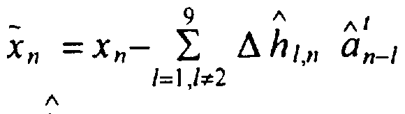
The Viterbi decoder operates on the signals { n } and determines the symbol sequence { a„ } which minimizes

The estimates of the channel impulse responses Δ ι0>,ι,ΔΛι,„, ΔΛ9,„ are deter- mined by an adaptive LMS algorithm such as to minimize ∑e„ .
To reduce implementation complexity, reduced-state Viterbi decoding is employed. State reduction is achieved by grouping the two states corresponding to the symbols +3 and -1 into one single state, and by grouping the two states corresponding to the symbols +1 and -3 into a second state. Note that state reduction requires that parallel transitions are resolved prior to the computation of the branch metrics. In order to reduce propagation delay, parallel transitions are resolved using the signal xn rather than x„ . This approach is justified by our earlier assumption that the channel impulse response does not significantly deviate from the impulse response of an ideal PRIV channel. Note also that since at any time instant only two states are retained, the difference of the survivor metrics can be propagated from one iteration to the next, rather than the survivor metrics themselves.
A block diagram with the main functions of the adaptive Viterbi decoder with auxiliary feedback filter can be developed by someone skilled in the art. In an adaptive survivor metric unit, the difference metric is iteratively computed, the extension of
Λ Λ the survivor sequences is determined, and the estimates Δ A0, „ and Δ hl n are obtained by an adaptive LMS algorithm. A path history unit is used to store the two survivor sequences. An adaptive auxiliary feedback filter computes the signal correction term
9 Λ ,
∑ Δ Λ/,„ a„.,
I=\ , l≠2 using tentative symbol decisions stored in the path history unit, and adaptively gen-
Λ Λ Λ erates the estimates Δ j]ιn , Δ /.3,„ , , Δ h9„ . No detailed implementations of the adaptive survivor metric unit, the path memory, and the adaptive auxiliary feedback filter are shown since these can be implemented by someone skilled in the art.
Mean-Squared Error Computation
The mean-squared error is computed in MSE meter 28 by low-pass filtering the metric increments. Such a device, again, can be implemented by someone skilled in the art and need therefore not be shown here in detail.
Descrambler and Differential Decoder
The bits representing the symbols output by the Viterbi decoder 27 are differentially decoded and descrambled by descrambler 29 which includes a descrambler whose transfer function is given by (l + D'3 + D28). The descrambler output signal represents the recovered information bits. This concludes the description of the partial- response system.
Full-Response System
An embodiment of the invention for a quaternary full-response system is shown in Fig.5 and described in the following. The filtering elements at the transmitter and the receiver must ensure that the signal yn obtained at the decision element of an adaptive digital equalizer 57, in the embodiment a DFE, is free from intersymbol interference. This signal is given by yn = aπ+ noise, where a„ e {-3,-l , + l, +3 } for quaternary modulation. In the embodiment, the linear forward equalizer of the
DFE is realized by a digital transversal filter.
Fig.5 gives an overview of a transceiver incorporating a full-response embodiment according to the invention. Each transceiver consists of a digital section 42, in which digital signal processing functions are performed, and a front-end section 43 for signal conversion, analog filtering, receiver clock generation, and cable driver/receiver functions.
In the transmitter, incoming quaternary symbols are represented by a 2-bit signal TDAT. These incoming information bits are scrambled in scrambler 44 using the polynomial l+ D'3 + D28and encoded by a 2B1Q differential encoder 45 to achieve transparency with respect to received signal polarity. After 2-bit digital-to-analog
conversion in D/A converter 46, the resulting signal is shaped by a fixed transmit filter 47, then amplified by power amplifier 48, and transmitted via cable 41.
An incoming signal - from cable 41 - is amplified by variable gain amplifier (VGA) 49 and filtered by a fixed analog filter 51. A control voltage determines the frequency- independent gain of VGA 49. The control signal for the VGA is derived digitally.
Received signal samples xn are obtained in analog-to-digital (A/D) converter 52 by 6-bit A/D conversion at a rate of MT symbols per second. The sampling phase of A/D converter 52 is determined by a voltage-controlled oscillator (VCO) 53 whose control voltage is adjusted by the disclosed decision-directed timing recovery algo- rithm. To simplify conversion, the control voltage for VCO 53 is provided by control circuit 59 in binary sigma-delta modulated form, as is the control voltage for VGA 49. Two sigma-delta demodulators 54 and 56 serve to derive the required analog control voltages.
Self-Training Equalization for Full-Response Systems The thus derived 6-bit-wide signal samples xn are transferred into the delay line of the linear forward equalizer of an adaptive equalizer 57, here a decision feedback equalizer (DFE). The output of this equalizer is given by v = c x - dj b „ , wherein
c = {c0 n cNΛ „ } denotes the vector of coefficients of the linear forward equalizer,
&I = i „ - •••• dLΛ n } denotes the vector of coefficients of the feedback filter, x = {xn xπ Λ,+1 } represents the vector of signals stored in the equalizer delay line at time n , and b = {ύπ l όn L+i } represents the vector of tentative quaternary decisions stored in the feedback filter delay line at time n.
Traditionally, the LMS algorithm described in E. A. Lee, and D. G. Messerschmitt, cited above, Ch. 9, is employed for decision-directed adjustment of the DFE coefficients: cπ+1 = cn- α^ tn xn ,
where α^ is the adaptation gain and en an error signal given by &„ = yn - bn.
If the DFE operates in self-training mode, the coefficients of the feedback filter are normally set to zero; then the output of the equalizer is given by yn = cπ τ xn.
For self training, we cannot rely on the correctness of decisions ύπ , and hence on the error signals n . We will use instead of ύn a pseudo error defined by ( y„ - b„ if [vπ\ > 3
( - δ„ sιgn(yn) otherwise, where δπ is a parameter in the range (0. δm , δm r > 0. The parameter is updated at each iteration as follows:
= ( δ„ - 3Δ if iv > 3, "4 | ( δ + Δ otherwise, and Δ is a small positive constant
The generation of the pseudo error J., is based on a priori knowledge of the statistics of the signal. In the case of accomplished equalization, yn corresponds to the quaternary channel input symbols ar embedded in noise. Therefore, whenever the event \yn\ > 3 is observed, we can use yn - ύn as a trusted error to update the equalizer coefficients. If we observe the event yn\ < 3, no trusted error is available. In this case, we choose to update the equalizer coefficients so that the probabilities of the events \yπ\ < 3 and \yn\ > 3 assume the values 3/4 and 1/4 , respectively, which are the probabilities of these events for an ideally equalized noisy quaternary signal, provided that the input symbols form a sequence of independent identically distributed random variables. This is achieved by setting the pseudo error equal to δπ sign(yπ) whenever \yπ\ < 3 and updating the value of δ„at each iteration so that δn becomes larger if the event \yn\ < 3 occurs more often than expected, and δπ becomes smaller otherwise.
The algorithm for self-training adaptive equalization is then given by c„+l = cπ- st εn xn , where st is the adaptation gain during self training.
Several variants of the algorithm can be obtained through different simplifications. For example, pseudo errors can be computed based on the signal energy at the equalizer output. If the signal energy is found to be too often below a given threshold, the error term is set equal to - c sιgn(yn), where c is a positive constant, whenever \yn\ < 3 , and trusted errors are used when \yn\ > 3 .
In this embodiment, symbol-rate sampling at the receiver is assumed . In practice, it is common to sample the received signal at a rate larger than the symbol rate and employ fractionally-spaced equalization. The extension of the described self- training algorithm to this case is straightforward.
An estimate of the average squared error signal (MSE) at the decision point is computed in MSE meter 50 to monitor the "transmission-link quality". If the MSE drops below a given threshold, tentative decisions on the transmitted symbols are sufficiently reliable. Then the DFE enters decision-directed mode and updating of all DFE coefficients by the LMS algorithm takes place.
As an alternative to the above described freezing the coefficients of the feedback filter in the self-training mode, these coefficients can be updated also during self training by ύfπ+ 1 = dn + sl εn bn .
The signals at the output of the decision feedback filter are differentially decoded and descrambled in descrambler 60. The recovered quaternary symbols are represented by the two-bit signal RDAT at the output of the digital section 42 of the transceiver.
Light line 61 in Fig.5 carries a receiver clock signal RCLK' produced by VCO 53; this clock signal RCLK' controls all digital receiver functions. In the transmit section of the transceiver, an externally provided transmitter clock signal TCLK' serves the same function, as indicated.
The invention has been shown and explained with reference to the drawings and the underlying theoretical considerations; these details, however, are not intended to limit the scope of the invention as defined in the appended claims.
Claims
CLAIMS 1. A method for achieving timing recovery in a receiver of a digital communication system, characterized by controlling the sampling time of an analog/digital converter (22, 5 52) in said receiver by means of a gradient defined as
wherein x s the signal sample at the output of said converter (22, 52) at time n, by e„ = x„-s„ , s„ being a tentative decision on the  received signal, g\(e„ ) is a function of said error term, and g2( s„ ) is a function of said tentative decision.
102. The method of claim 1 , wherein the function  e„ ) is defined as gι( e» ) = e» -
3. The method of claim 1 , wherein the function g2( s„ ) is defined as g2( -?„ ) = ! -?„ Im, m being larger than 1 , preferably at least 2.
4. A method for detecting and recovering signals in a receiver of a communication 15 system with a timing recovery scheme according to any of claims 1 to 3, adapted for partial-response transmission, said receiver including a variable gain amplifier (19), a variable filter (20), and the analog/digital converter (22), characterized by
- forming an estimate of the time-discrete autocorrelation function R^ (tJ' of a re-
20 ceived signal, the value of said function for t' = IcT being given by the expected value of the product of the signal samples taken at the output of said analog/digital converter (22) at time / and at time t+kT, T being the modulation interval,
- controlling said variable gain amplifier (19) by a first value being derived from said estimate of the time-discrete autocorrelation function Λw (f), preferably by a value
25 derived from said estimate at = 0, - controlling said variable filter (20) by a second value being derived from said estimate of the time-discrete autocorrelation function R^ (t preferably by a value derived from said estimate at /' = T.
5. Apparatus for detecting and recovering received signals in a partial-response 5 communication system, said apparatus including a variable gain amplifier (19), a variable filter (20) and an analog/digital converter (22), further comprising
- means (29) for producing an estimate of the time-discrete autocorrelation function R^ (V) of a received signal, the value of said estimate for /' = kT being given by the product of a digital signal sample taken at the output of said analog/digital con-
10 verter (22) at time / with a signal sample taken at time t+kT,
- means (26, 29) for controlling the gain of said amplifier (19) by a first voltage being derived from a first value of said estimate of RB (tJ' , preferably by a value derived from said estimate at /' = 0,
- means (25, 29) for controlling the transfer characteristics of said variable filter (20) 15 using a second voltage being derived from a second value of said estimate of
R t)' , preferably by a value derived from said estimate at /' - 7', and
- means (23, 24, 29) for controlling the sampling time of said analog/digital converter (22) by a third voltage being derived according to the timing recovery method of any of the claims 1 to 3.
206. A method for detecting and recovering signals in a partial response communication system with a timing recovery scheme according to any of the claims 1 to 3, said receiver including a variable gain amplifier (19), a variable analog forward filter (20), an analog/digital converter (22), and a component (27) with a decision element and an adaptive feedback filter, altogether forming a "decision feedback equalizer" (DFE), the method comprising, for achieving initial DFE convergence in a self-training mode,
- forming an estimate of the time-discrete autocorrelation function R t') of a received signal, the value of said function for t' = kT being given by the expected value of the product of the signal samples taken at the output of said analog/digital converter (22) at time rand at time t+kT,
- controlling said variable gain amplifier (19) by a first value being derived from said estimate of the time-discrete autocorrelation function R^ (f), preferably by a value derived from said estimate at t' = 0, and
- controlling said variable filter (20) by a second value being derived from said estimate of the time-discrete autocorrelation function R^ (t'J, preferably by a value derived from said estimate at t' = T.
7. The method according to claim 6, wherein the feedback filter is embedded in a Viterbi decoder, preferably a reduced-state Viterbi decoder, for maximum-likelihood sequence detection.
8. Apparatus for detecting and recovering received signals in a partial response communication system, said apparatus including a variable gain amplifier (19), a variable analog forward filter (20), an analog/digital converter (21), and a component (27) including a decision element and an adaptive digital feedback filter, alto- gether forming a "decision feedback equalizer" (DFE), the apparatus further comprising, for achieving initial DFE convergence in a self-training mode,
- means (29) for producing an estimate of the time-discrete autocorrelation function R^ (t') of a received signal, the value of said estimate for /' = kT being given by the product of a digital signal sample taken at the output of said analog/digital con- verter (21) at time / with a signal sample taken at time t+kT, - means (26, 29) for controlling the gain of said amplifier (19) by a first voltage, said first voltage being derived from a first value of said estimate of /?β ft)' , preferably by a value derived from said estimate at /' = 0, and
- means (25, 29) for controlling the transfer characteristics of said filter (20) using a 5 second voltage, said second voltage being derived from a second value of said estimate of R^ (t'J, preferably by a value derived from said estimate at /' = T.
9. The apparatus of claim 8, wherein the component (27) includes a Viterbi decoder, preferably a reduced-state Viterbi decoder, with a digital feedback filter embedded in said Viterbi decoder.
10 10. The method according to any of the claims 4, 6, or 7, wherein the variable gain amplifier (19) is controlled conforming to
U = u vGA.,1 - OLGΔU VGA.,, , 0 < αG « 1 ,
UIGΛ , being the voltage controlling said variable gain amplifier (19) at time nT,
15 αc being the adaptation gain, and
Δu vGA.n being the adjustment term.
11. The method according to any of the claims 4, 6, or 7, wherein the variable filter (20) is controlled conforming to
UEQZ,n+\ - EQZ,n ~ .EΔuEQZ„ - 0 < Ot£ « 1 ,
20 uEQz, being the voltage controlling said variable filter (20) at time nT,
CLE being the adaptation gain, and
ΔUEQZ,„ being the adjustment term.
12. The apparatus of any of the claims 5, 8 or 9, wherein one or more sigma-delta demodulators (24, 25, 26) are provided to derive analog control voltages, the input WO 98 09400 PCT IB96ΛK)873
26 to the demodulator (26) associated with the variable gain amplifier (19) being controlled according to
U VGAS+\ = U VGAJX - GΔU VGA* , 0 < αG « 1 ,
uvGAs, determining the voltage controlling said variable gain amplifier (19), αG being the adaptation gain,
Δu vGAjn being the adjustment term,
and/or the input to the demodulator (25) associated with variable filter (20) being controlled according to
UEQZ*+\ = UEQZ,n ~ OLEΔUEQZSI , 0 < 0t£ « 1 ,
uEQZjt determining the voltage controlling said variable filter (20),
OLE being the adaptation gain, and
ΔU QZ,„ being the gradient term.
13. A method for detecting and recovering signals in a receiver of a communication system with a timing recovery scheme according to any of claims 1 to 3, adapted for full-response M-ary transmission, said receiver including a variable gain amplifier (49), an analog/digital converter (52), and an adaptive equalizer (57) with a linear forward filter and a decision element, the method comprising, for achieving initial convergence in a self-training mode, - forming a pseudo-error ε„ defined by
_ ( yn - bn if \yπ\ > M -1 ε. =
( - δπ sign(yn) otherwise, where yn is the output of said equalizer (57), bn is a tentative M-ary decision, and δπ is a positive parameter updated at each iteration according to ( δ„ - Δ, if |y > M -1
( δπ + Δ2 otherwise,
Δ, and Δ2 being positive constants, - updating the vector cn of the coefficients of said linear forward filter according to
£„+1 = n- sl εn xπ , where sl is the adaptation gain and xn is the vector of signal samples taken at the output of said converter (52).
14. The method according to claim 13, the adaptive equalizer (57) further including a feedback filter, wherein the vector dn of the coefficients of said feedback filter, for achieving initial convergence in a self-training mode, is updated according to
— d n„++l 1 = — d n + a j*o ε n„ — b π.1 where bn is the vector of tentative decisions and α^ is an adaptation gain for the feedback filter which can be either positive or zero
15. Apparatus for detecting and recovering received signals in a full-response communication system, said apparatus including a variable gam amplifier (49), an analog/digital converter (52), and an adaptive equalizer (57) with a linear forward filter and a decision element, comprising, for achieving initial convergence in a self- training mode, in said adaptive equalizer (57)
- means for forming a pseudo-error εn defined by
= ( yn - bn if yn\ > M -1
( - δn sιgn(y otherwise, where δ„ is the output of said equalizer (57), bn is a tentative M-ary decision, and δ„ is a positve parameter updated at each iteration according to δ = ( δ„ - Δ, if \yn\ > M -1,
( δπ + Δ2 otherwise,
Δ,and Δ2 being positive constants,
- means for updating the vector cπ of the coefficients of said linear forward filter according to
— c π+,l = — c n - α st, ε n x — π ,' where sl is the adaptation gain and xn is the vector of signal samples taken at the output of said converter (52).
16. The apparatus according to claim 15, the adaptive equalizer (57) further including a feedback filter and means for updating the vector dn of the coefficients of said feedback filter according to dn+ ] = dn + b εn bπ , where bn is the vector of tentative decisions and α^ is an adaptation gain for the feedback filter which can be either positive or zero.
Priority Applications (1)
| Application Number | Priority Date | Filing Date | Title |
|---|---|---|---|
| PCT/IB1996/000873 WO1998009400A1 (en) | 1996-08-30 | 1996-08-30 | Receiving and equalizing signals for high-speed data transmission |
Applications Claiming Priority (1)
| Application Number | Priority Date | Filing Date | Title |
|---|---|---|---|
| PCT/IB1996/000873 WO1998009400A1 (en) | 1996-08-30 | 1996-08-30 | Receiving and equalizing signals for high-speed data transmission |
Publications (1)
| Publication Number | Publication Date |
|---|---|
| WO1998009400A1 true WO1998009400A1 (en) | 1998-03-05 |
Family
ID=11004466
Family Applications (1)
| Application Number | Title | Priority Date | Filing Date |
|---|---|---|---|
| PCT/IB1996/000873 WO1998009400A1 (en) | 1996-08-30 | 1996-08-30 | Receiving and equalizing signals for high-speed data transmission |
Country Status (1)
| Country | Link |
|---|---|
| WO (1) | WO1998009400A1 (en) |
Cited By (8)
| Publication number | Priority date | Publication date | Assignee | Title |
|---|---|---|---|---|
| FR2786349A1 (en) * | 1998-10-14 | 2000-05-26 | Samsung Electronics Co Ltd | DECISION FEEDBACK EQUALIZER AND INDEX COEFFICIENT UPDATE METHOD THEREOF |
| WO2000065772A2 (en) * | 1999-04-22 | 2000-11-02 | Broadcom Corporation | Phy control module for a multi-pair gigabit transceiver |
| US6363129B1 (en) | 1998-11-09 | 2002-03-26 | Broadcom Corporation | Timing recovery system for a multi-pair gigabit transceiver |
| EP1420556A2 (en) * | 2002-11-15 | 2004-05-19 | STMicroelectronics, Inc. | Filter bank for long Ethernet links |
| US6928106B1 (en) | 1998-08-28 | 2005-08-09 | Broadcom Corporation | Phy control module for a multi-pair gigabit transceiver |
| US7634001B2 (en) | 1998-08-28 | 2009-12-15 | Broadcom Corporation | Dynamic regulation of power consumption of a high-speed communication system |
| US7778313B2 (en) | 1998-08-28 | 2010-08-17 | Broadcom Corporation | PHY control module for a multi-pair gigabit transceiver |
| WO2013158106A1 (en) | 2012-04-19 | 2013-10-24 | Intel Corporation | Unequalized clock data recovery for serial i/o receiver |
Citations (1)
| Publication number | Priority date | Publication date | Assignee | Title |
|---|---|---|---|---|
| EP0729251A2 (en) * | 1995-02-24 | 1996-08-28 | Matsushita Electric Industrial Co., Ltd. | Data reproducing method and data reproducing unit with sampling |
-
1996
- 1996-08-30 WO PCT/IB1996/000873 patent/WO1998009400A1/en active Application Filing
Patent Citations (1)
| Publication number | Priority date | Publication date | Assignee | Title |
|---|---|---|---|---|
| EP0729251A2 (en) * | 1995-02-24 | 1996-08-28 | Matsushita Electric Industrial Co., Ltd. | Data reproducing method and data reproducing unit with sampling |
Non-Patent Citations (1)
| Title |
|---|
| CHERUBINI G ET AL: "ADAPTIVE ANALOG EQUALIZATION AND RECEIVER FRONT-END CONTROL FOR MULTILEVEL PARTIAL-RESPONSE TRANSMISSION OVER METALLIC CABLES", IEEE TRANSACTIONS ON COMMUNICATIONS, vol. 44, no. 6, 1 June 1996 (1996-06-01), pages 675 - 685, XP000599965 * |
Cited By (18)
| Publication number | Priority date | Publication date | Assignee | Title |
|---|---|---|---|---|
| US7778313B2 (en) | 1998-08-28 | 2010-08-17 | Broadcom Corporation | PHY control module for a multi-pair gigabit transceiver |
| US6928106B1 (en) | 1998-08-28 | 2005-08-09 | Broadcom Corporation | Phy control module for a multi-pair gigabit transceiver |
| US8077762B2 (en) | 1998-08-28 | 2011-12-13 | Broadcom Corporation | PHY control module for a multi-pair gigabit transceiver |
| US7443910B2 (en) | 1998-08-28 | 2008-10-28 | Broadcom Corporation | PHY control module for a multi-pair gigabit transceiver |
| US7634001B2 (en) | 1998-08-28 | 2009-12-15 | Broadcom Corporation | Dynamic regulation of power consumption of a high-speed communication system |
| US7672368B2 (en) | 1998-08-28 | 2010-03-02 | Broadcom Corporation | PHY control module for a multi-pair gigabit transceiver |
| FR2786349A1 (en) * | 1998-10-14 | 2000-05-26 | Samsung Electronics Co Ltd | DECISION FEEDBACK EQUALIZER AND INDEX COEFFICIENT UPDATE METHOD THEREOF |
| US6807229B1 (en) | 1998-10-14 | 2004-10-19 | Samsung Electronics Co., Ltd. | Decision feedback equalizer and method for updating tap coefficients thereof |
| US6363129B1 (en) | 1998-11-09 | 2002-03-26 | Broadcom Corporation | Timing recovery system for a multi-pair gigabit transceiver |
| US7116742B2 (en) | 1998-11-09 | 2006-10-03 | Broadcom Corporation | Timing recovery system for a multi-pair gigabit transceiver |
| WO2000065772A2 (en) * | 1999-04-22 | 2000-11-02 | Broadcom Corporation | Phy control module for a multi-pair gigabit transceiver |
| WO2000065772A3 (en) * | 1999-04-22 | 2002-01-03 | Broadcom Corp | Phy control module for a multi-pair gigabit transceiver |
| EP1420556A2 (en) * | 2002-11-15 | 2004-05-19 | STMicroelectronics, Inc. | Filter bank for long Ethernet links |
| EP1420556A3 (en) * | 2002-11-15 | 2007-04-11 | STMicroelectronics, Inc. | Filter bank for long Ethernet links |
| WO2013158106A1 (en) | 2012-04-19 | 2013-10-24 | Intel Corporation | Unequalized clock data recovery for serial i/o receiver |
| EP2839582A4 (en) * | 2012-04-19 | 2015-12-16 | Intel Corp | Unequalized clock data recovery for serial i/o receiver |
| US9479364B2 (en) | 2012-04-19 | 2016-10-25 | Intel Corporation | Unequalized clock data recovery for serial I/O receiver |
| US10009194B2 (en) | 2012-04-19 | 2018-06-26 | Intel Corporation | Unequalized clock data recovery for serial I/O receiver |
Similar Documents
| Publication | Publication Date | Title |
|---|---|---|
| US5742642A (en) | Signal processing method and apparatus for reducing equalizer error | |
| US7616686B2 (en) | Method and apparatus for generating one or more clock signals for a decision-feedback equalizer using DFE detected data | |
| JP3023616B2 (en) | Adaptive noise prediction partial response equalization for channels with spectral nulls | |
| AU709892B2 (en) | Method and apparatus for timing recovery | |
| CN113472708B (en) | Eye monitor for parallel digital equalizer | |
| US7606301B2 (en) | Method and apparatus for adaptively establishing a sampling phase for decision-feedback equalization | |
| US10447509B1 (en) | Precompensator-based quantization for clock recovery | |
| US20010031020A1 (en) | Baud-rate timing recovery | |
| Dolivo et al. | Fast timing recovery for partial-response signaling systems | |
| US11570024B2 (en) | Equalizer with perturbation effect based adaptation | |
| WO1998009400A1 (en) | Receiving and equalizing signals for high-speed data transmission | |
| US11231740B2 (en) | Clock recovery using between-interval timing error estimation | |
| US7251274B1 (en) | Multichannel adaptive equaliser | |
| EP0389027B1 (en) | Procedure and device for timing recovery in the reception of base band digital signals | |
| US6519282B1 (en) | Method for digital transmission of information | |
| EP0800735A1 (en) | Adaptive equalization for priv transmission systems | |
| Cherubini et al. | A quaternary partial-response class-IV system for 125 Mbit/s data transmission over unshielded twisted-pair cables | |
| Proakis et al. | Adaptive equalization algorithms for high rate underwater acoustic communications | |
| US7321618B2 (en) | PCM upstream data transmission server | |
| Lin et al. | Full-duplex data over local loops | |
| ARIMOTO | Equalization, Adaptive (see Adaptive Equalization | |
| CN116582189A (en) | Conversion between signal constellations | |
| Young et al. | Equaliser timing considerations for microwave digital radio during deep multipath fading | |
| Barry et al. | Timing recovery | |
| Cherubini et al. | A Quaternary Partial-Response Class-IV Transceiver for 125 Mbit/s Data ission over Unshielded Twisted-Pair Cables: rinciples of Operation and VLSI Realization |
Legal Events
| Date | Code | Title | Description |
|---|---|---|---|
| AK | Designated states |
Kind code of ref document: A1 Designated state(s): JP KR US |
|
| AL | Designated countries for regional patents |
Kind code of ref document: A1 Designated state(s): AT BE CH DE DK ES FI FR GB GR IE IT LU MC NL PT SE |
|
| WWE | Wipo information: entry into national phase |
Ref document number: 09066475 Country of ref document: US |
|
| 121 | Ep: the epo has been informed by wipo that ep was designated in this application | ||
| NENP | Non-entry into the national phase |
Ref country code: JP Ref document number: 98511411 Format of ref document f/p: F |
|
| NENP | Non-entry into the national phase |
Ref country code: CA |
|
| 122 | Ep: pct application non-entry in european phase |