WO2001061917A1 - Consumable authentication protocol and system - Google Patents
Consumable authentication protocol and system Download PDFInfo
- Publication number
- WO2001061917A1 WO2001061917A1 PCT/AU2001/000139 AU0100139W WO0161917A1 WO 2001061917 A1 WO2001061917 A1 WO 2001061917A1 AU 0100139 W AU0100139 W AU 0100139W WO 0161917 A1 WO0161917 A1 WO 0161917A1
- Authority
- WO
- WIPO (PCT)
- Prior art keywords
- chip
- authentication
- key
- random number
- consumable
- Prior art date
Links
Classifications
-
- H—ELECTRICITY
- H04—ELECTRIC COMMUNICATION TECHNIQUE
- H04L—TRANSMISSION OF DIGITAL INFORMATION, e.g. TELEGRAPHIC COMMUNICATION
- H04L9/00—Cryptographic mechanisms or cryptographic arrangements for secret or secure communications; Network security protocols
- H04L9/32—Cryptographic mechanisms or cryptographic arrangements for secret or secure communications; Network security protocols including means for verifying the identity or authority of a user of the system or for message authentication, e.g. authorization, entity authentication, data integrity or data verification, non-repudiation, key authentication or verification of credentials
- H04L9/3271—Cryptographic mechanisms or cryptographic arrangements for secret or secure communications; Network security protocols including means for verifying the identity or authority of a user of the system or for message authentication, e.g. authorization, entity authentication, data integrity or data verification, non-repudiation, key authentication or verification of credentials using challenge-response
-
- H—ELECTRICITY
- H04—ELECTRIC COMMUNICATION TECHNIQUE
- H04L—TRANSMISSION OF DIGITAL INFORMATION, e.g. TELEGRAPHIC COMMUNICATION
- H04L9/00—Cryptographic mechanisms or cryptographic arrangements for secret or secure communications; Network security protocols
- H04L9/002—Countermeasures against attacks on cryptographic mechanisms
-
- H—ELECTRICITY
- H04—ELECTRIC COMMUNICATION TECHNIQUE
- H04L—TRANSMISSION OF DIGITAL INFORMATION, e.g. TELEGRAPHIC COMMUNICATION
- H04L9/00—Cryptographic mechanisms or cryptographic arrangements for secret or secure communications; Network security protocols
- H04L9/32—Cryptographic mechanisms or cryptographic arrangements for secret or secure communications; Network security protocols including means for verifying the identity or authority of a user of the system or for message authentication, e.g. authorization, entity authentication, data integrity or data verification, non-repudiation, key authentication or verification of credentials
- H04L9/3247—Cryptographic mechanisms or cryptographic arrangements for secret or secure communications; Network security protocols including means for verifying the identity or authority of a user of the system or for message authentication, e.g. authorization, entity authentication, data integrity or data verification, non-repudiation, key authentication or verification of credentials involving digital signatures
-
- H—ELECTRICITY
- H04—ELECTRIC COMMUNICATION TECHNIQUE
- H04L—TRANSMISSION OF DIGITAL INFORMATION, e.g. TELEGRAPHIC COMMUNICATION
- H04L2209/00—Additional information or applications relating to cryptographic mechanisms or cryptographic arrangements for secret or secure communication H04L9/00
- H04L2209/04—Masking or blinding
- H04L2209/043—Masking or blinding of tables, e.g. lookup, substitution or mapping
-
- H—ELECTRICITY
- H04—ELECTRIC COMMUNICATION TECHNIQUE
- H04L—TRANSMISSION OF DIGITAL INFORMATION, e.g. TELEGRAPHIC COMMUNICATION
- H04L2209/00—Additional information or applications relating to cryptographic mechanisms or cryptographic arrangements for secret or secure communication H04L9/00
- H04L2209/26—Testing cryptographic entity, e.g. testing integrity of encryption key or encryption algorithm
Definitions
- This invention concerns a consumable authentication protocol for validating the existence of an untrusted authentication chip, as well as ensuring that the authentication chip lasts only as long as the consumable.
- it concerns a consumable authentication system for the protocol.
- Authentication is an extremely large and constantly growing field. This invention is concerned with authenticating consumables. In most cases, there is no reason to prohibit the use of consumables in a third party product.
- the invention concerns an authentication chip that contains an authentication code and circuit specially designed to prevent copying.
- the chip is manufactured using the standard Flash memory manufacturing process, and is low cost enough to be included in consumables such as ink and toner cartridges.
- the authentication chips are compliant with the NSA export guidelines since they do not constitute an encryption device. They can therefore be practically manufactured in the USA (and exported) or anywhere else in the world.
- a message, denoted by M, is plaintext.
- the process of transforming M into ciphertext C, where the substance of M is hidden, is called encryption.
- the process of transforming C back into M is called decryption.
- E the encryption function
- D the decryption function
- a symmetric encryption algorithm is one where:
- K • K] can be derived from K 2 .
- Ki K 2 .
- K K 2 .
- K The security of these algorithms rests very much in the key K. Knowledge of K allows anyone to encrypt or decrypt. Consequently K must remain a secret for the duration of the value of M.
- M may be a wartime message "My current position is grid position 123-456". Once the war is over the value of M is greatly reduced, and if K is made public, the knowledge of the combat unit's position may be of no relevance whatsoever. Of course if it is politically sensitive for the combat unit's position to be known even after the war, K may have to remain secret for a very long time.
- IDEA 3.3.1 DES DES Data Encryption Standard
- IDEA 3.3.1 DES DES Data Encryption Standard
- the key length is 56 bits. It has been implemented in hardware and software, although the original design was for hardware only. The original algorithm used in DES was patented in 1976 (US patent number 3,962,539) and has since expired.
- triple-DES gives protection of equivalent key length of 112 bits [78]
- Triple-DES does not give the equivalent protection of a 168-bit key (3x56) as one might naively expect Equipment that performs triple-DES decoding and/or encoding cannot be exported from the United
- Blowfish is a symmetric block cipher first presented by Schneier in 1994 [76] It takes a variable length key, from 32 bits to 448 bits, is unpatented, and is both license and royalty free In addition, it is much faster than DES
- the Blowfish algorithm consists of two parts a key-expansion part and a data-encryption part Key expansion converts a key of at most 448 bits into several subkey arrays totaling 4168 bytes Data encryption occurs via a 16-round Feistel network All operations are XORs and additions on 32-bit words, with four index array lookups per round It should be noted that decryption is the same as encryption except that the subkey arrays are used in the reverse order Complexity of implementation is therefore reduced compared to other algorithms that do not have such symmetry
- RC5 Designed by Ron Rivest in 1995, RC5 [74] has a variable block size, key size, and number of rounds Typically, however, it uses a 64-bit block size and a 128-bit key
- the subkey arrays total 136 bytes
- Data encryption uses addition mod 2w, XOR and bitwise rotation
- IDEA uses 128-bit keys to operate on 64-bit plaintext blocks The same algorithm is used for encryption and decryption It is generally regarded as the most secure block algorithm available today [78][56]
- An asymmetric encryption algorithm is one where
- DSA Digital Signature Algorithm
- DSA DSA
- DSA explicitly uses the SHA-1 hashing algorithm (see
- DSA key generation relies on finding two primes p and q such that q divides p-l. According to Schneier [78], a 1024-bit p value is required for long term DSA security. However the DSA standard [29] does not permit values of p larger than 1024 bits (p must also be a multiple of 64 bits).
- the ElGamal scheme [22][23] is used for both encryption and digital signatures.
- the security is based on the conjectured difficulty of calculating discrete logarithms in a finite field.
- the public key is y, g, and p.
- the private key is x.
- ElGamal is unpatented. Although it uses the patented Diffie-Hellman public key algorithm [15][16], those patents expired in 1997. ElGamal public key encryption and digital signatures can now be safely used without infringing third party patents.
- the general principle of a challenge-response protocol is to provide identity authentication.
- the simplest form of challenge-response takes the form of a secret password.
- A asks B for the secret password, and if B responds with the correct password, A declares B authentic.
- B There are three main problems with this kind of simplistic protocol. Firstly, once B has responded with the password, any observer C will know what the password is. Secondly, A must know the password in order to verify it. Thirdly, if C impersonates A, then B will give the password to C (thinking C was A), thus compromising the password.
- cryptographic challenge-response protocols proves its identity to another (the verifier) by demonstrating knowledge of a secret known to be associated with that entity, without revealing the secret itsel ' to the verifier during the protocol [56].
- the verifier knows the secret, while in others the secret is not even known by the verifier
- the Zero Knowledge Proof protocol first described by Feige, Fiat and Shamir in [24] is extensively used in Smart Cards for the purpose of authentication [34] [36] [67]
- the protocol s effectiveness is based on the assumption that it is computationally infeasible to compute square roots modulo a large composite integer with unknown factorization This is provably equivalent to the assumption that facto ⁇ ng large integers is difficult
- a one-way function F operates on an input X, and returns F[X] such that X cannot be determined from F[X]
- F[X] contains fewer bits than X
- collisions must exist
- X contains more bits than F[X]
- the input must be compressed in some way to create the output
- X is broken into blocks of a particular size, and compressed over a number of rounds, with the output of one round being the input to the next
- the output of the hash function is the last output once X has been consumed
- a pseudo-collision of the compression function CF is defined as two different initial values V !
- Hash Functions • Message Authentication Codes
- Symmetric encryption algorithms have the advantage over asymmetric algorithms (see Section 3 4) for producing one-way functions based on encryption for the following reasons-
- Blum, Blum and Shub define the ideal generator as follows. “... we would like a pseudo-random sequence generator to quickly produce, from short seeds, long sequences (of bits) that appear in every way to be generated by successive flips of a fair coin” . They defined the x 2 mod n generator [10], more commonly referred to as the BBS generator. They showed that given certain assumptions upon which modern cryptography relies, a BBS generator passes extremely stringent statistical tests.
- the initial state of the generator is given by x 0 where x 0
- [68] describes a problem in selecting x.
- the nature of the problem is that a BBS generator does not create a single cycle of known length. Instead, it creates cycles of various lengths, including degenerate (zero-length) cycles. Thus a BBS generator cannot be initialized with a random state - it might be on a short cycle.
- Specific algorithms exist in section 9 of [10] to determine the length of the period for a given seed given certain strenuous conditions for n.
- Hash functions map arbitrary length messages to fixed-length hash values.
- Hash functions are referred to as H[M]. Since the input is of arbitrary length, a hash function has a compression component in order to produce a fixed length output. Hash functions also have an obfuscation component in order to make it difficult to find collisions and to determine information about M from H[M].
- the primary application for hash functions is in the reduction of an input message into a digital "fingerprint" before the application of a digital signature algorithm.
- One problem of collisions with digital signatures can be seen in the following example.
- A has a long message Ml that says "/ owe B $10".
- A signs H[M ⁇ ] using his private key.
- M 2 is favorable to B, for example "/ owe B $1 million”.
- collision resistant one-way hash functions are SHA-1 [28], MD5 [73] and RfPEMD-160 [66], all derived from MD4 [70] [72].
- 3.6.3.1MD4 Ron Rivest introduced MD4 [70][72] in 1990. It is only mentioned here because all other one-way hash functions are derived in some way from MD4.
- MD4 is now considered completely broken [18][19] in that collisions can be calculated instead of searched for.
- B could trivially generate a substitute message M 2 with the same hash value as the original message M].
- MD5 Ron Rivest introduced MD5 [73] in 1991 as a more secure MD4. Like MD4, MD5 produces a 128- bit hash value. MD5 is not patented [80].
- Dobbertin describes the status of MD5 after recent attacks [20]. He describes how pseudo-collisions have been found in MD5, indicating a weakness in the compression function, and more recently, collisions have been found. This means that MD5 should not be used for compression in digital signature schemes where the existence of collisions may have dire consequences. However MD5 can still be used as a one-way function. In addition, the HMAC-MD5 construct (see Section 3.6.4.1) is not affected by these recent attacks.
- SHA-1 SHA-1 [28] is very similar to MD5, but has a 160-bit hash value (MD5 only has 128 bits of hash value).
- SHA-1 was designed and introduced by the NIST and NSA for use in the Digital Signature Standard (DSS). The original published description was called SHA [27], but very soon afterwards, was revised to become SHA-1 [28], supposedly to correct a security flaw in SHA (although the NSA has not released the mathematical reasoning behind the change). There are no known cryptographic attacks against SHA-1 [78]. It is also more resistant to brute force attacks than MD4 or MD5 simply because of the longer hash result.
- NIST states in the same document [61] that DSA and SHA-1 do not infringe third party's rights: "NIST reviewed all of the asserted patents and concluded that none of them would be infringed by DSS. Extra protection will be written into the PK1 pilot project that will prevent an organization or individual from suing anyone except the government for patent infringement during the course of the project. "
- RIPEMD-160 is a hash function derived from its predecessor RIPEMD [11] (developed for the European Community's RTPE project in 1992). As its name suggests, RIPEMD-160 produces a 160-bit hash result Tuned for software implementations on 32-bit architectures, RIPEMD-160 is intended to provide a high level of security for 10 years or more
- RIPEMD-160 is in the public domain, and requires no licensing or royalty payments 3.6.4 Message Authentication Codes The problem of message authentication can be summed up as follows
- Hash functions such as MD5 rely on generating a hash value that is representative of the original input, and the original input cannot be derived from the hash value
- a simple attack by E, who is m-between A and B, is to intercept the message from B, and substitute his own Even if A also sends a hash of the original message, E can simply substitute the hash of his new message Using a one-way hash function alone, A has no way of knowing that B s message has been changed
- hash functions were never originally designed to contain a key or to support message authentication
- some ad hoc methods of using hash functions to perform message authentication including various functions that concatenate messages with secret prefixes, suffixes, or both have been proposed [56][78]
- Most of these ad hoc methods have been successfully attacked by sophisticated means [42][64][65]
- Additional MACs have been suggested based on XOR schemes [8] and Toephtz matrices [49] (including the special case of LFSR-based (Linear Feed Shift Register) constructions) 3.6.4.1 HMAC
- the HMAC construction [6] [7] in particular is gaining acceptance as a solution for Internet message authentication security protocols
- the HMAC construction acts as a wrapper, using the underlying hash function in a black-box way Replacement of the hash function is straightforward if desired due to security or performance reasons
- the major advantage of the HMAC construct is that it can be proven secure provided the underlying hash function has some reasonable cryptographic strengths - that is, HMAC's strengths are directly connected to the strength of the hash function [6 ⁇ Since the HMAC construct is a wrapper, any iterative hash function can be used in an HMAC
- H the hash function (e g MD5 or SHA-1)
- n number of bits output from H (e g 160 for SHA-1, 128 bits for MD5)
- M the data to which the MAC function is to be applied
- the HMAC algorithm is as follows 1 Extend K to 64 bytes by appending 0x00 bytes to the end of K
- HMAC[M] H[(K ® opad)
- the recommended key length is at least n bits, although it should not be longer than 64 bytes (the length of the hashing block) A key longer than n bits does not add to the security of the function
- HMAC optionally allows truncation of the final output e g truncation to 128 bits from 160 bits.
- the HMAC designers' Request for Comments [51] was issued m 1997, one year after the algorithm was first introduced The designers claimed that the strongest known attack against HMAC is based on the frequency of collisions for the hash function H (see Section 5 5 10), and is totally impractical for minimally reasonable hash functions
- HMAC protocols with replay prevention components [62] have been defined in order to prevent the capture and replay of any M, HMAC[M] combination within a given time period
- HMAC is in the public domain [50], and incurs no licensing fees
- Random number generators are also often used to generate keys Although Klapper has recently shown [45] that a family of secure feedback registers for the purposes of building key-streams does exist, he does not give any practical construction It is therefore best to say at the moment that all generators are insecure for this purpose For example, the Berlekamp-Massey algorithm [54], is a classic attack on an LFSR random number generator If the LFSR is of length n, then only 2n bits of the sequence suffice to determine the LFSR, compromising the key generator
- Generators include Blum, Blum, and Shub [10], stream ciphers such as RC4 by Ron Rivest [71], hash functions such as SHA-1 [28] and RIPEMD-160 [66], and traditional generators such LFSRs (Linear Feedback Shift Registers) [48] and their more recent counterpart FCSRs (Feedback with Carry Shift Registers) [44] 3.8 Attacks
- a known-plaintext attack is one where the attacker can see the data flow between the system and the authentication chip
- the inputs and outputs are observed (not chosen by the attacker), and can be analyzed for weaknesses (such as birthday attacks or by a search for differentially interesting input/output pairs)
- a known plaintext attack can be carried out by connecting a logic analyzer to the connection between the system and the authentication chip
- a chosen plaintext attack describes one where a cryptanalyst has the ability to send any chosen message to the cryptosystem, and observe the response If the cryptanalyst knows the algorithm, there may be a relationship between inputs and outputs that can be exploited by feeding a specific output to the input of another function
- the chosen plaintext attack is much stronger than the known plaintext attack since the attacker can choose the messages rather than simply observe the data flow
- it is generally very difficult to prevent chosen plaintext attacks since the cryptanalyst can logically pretend he/she is the system, and thus send any chosen bit-pattern streams to the authentication chip
- attackers can gather valuable information from the results of a bad input This can range from the error message text to the time taken for the error to be generated
- algo ⁇ th ⁇ uc time can be seen with an algo ⁇ thm that returns an error as soon as an erroneous bit is detected m the input message
- it may be a simple method for the attacker to time the response and alter each bit one by one depending on the time taken for the error response, and thus obtain the key
- the time taken can be observed with far greater accuracy than over the Internet
- the weakening of an n-bit key by the birthday attack is 2 ⁇ /2 .
- a key length of 128 bits that is susceptible to the birthday attack has an effective length of only 64 bits.
- the number of choices for a particular block is based on the length of the block. If the chaining variable is c bits, the hashing function behaves like a random mapping, and the block length is b bits, the number of such b-bit blocks is approximately 2 b 12 C .
- the challenge for finding a substitution block is that such blocks are a sparse subset of all possible blocks.
- the number of 512 bit blocks is approximately 2 512 /2 160 , or 2 352 .
- the chance of finding a block by brute force search is about 1 in 2 160 .
- the clone manufacturer need simply provide a lookup table that contains values for past and predicted future serial numbers. There are unlikely to be more than 10 9 of these. • If the test code is simply the date, then the clone manufacturer can produce a lookup table using the date as the address
- test code is a pseudo-random number using either the serial number or the date as a seed
- the clone manufacturer just needs to crack the pseudo-random number generator in the system This is probably not difficult, as they have access to the object code of the system
- the clone manufacturer would then produce a content addressable memory (or other sparse array lookup) using these codes to access stored authentication codes 3.8.1.13 Differential cryptanalysis
- Differential cryptanalysis desc ⁇ bes an attack where pairs of input streams are generated with known differences, and the differences in the encoded streams are analyzed
- a man-in-the-middle can substitute part or all of a message This is where a real authentication chip is plugged into a reusable clone chip with the consumable The clone chip intercepts all messages between the system and the authentication chip, and can perform a number of substitution attacks
- a reusable consumable with a clone authentication chip may make use of a real authentication chip
- the clone authentication chip uses the real chip for the authentication call, and then simulates the real authentication chip s state data after that
- a clone authentication chip can accomplish a simple authentication bypass by simulating a loss of connection after the use of the consumable but before the authentication protocol has completed (or even started)
- Reading ROM describes an attack when keys are stored in ROM, while the remaining attacks assume that a secret key is stored in Flash memory
- ROM If a key is stored in ROM it can be read directly A ROM can thus be safely used to hold a public key (for use in asymmetric cryptography), but not to hold a private key In symmetric cryptography, a ROM is completely insecure Using a copyright text (such as a haiku) as the key is not sufficient, because we are assuming that the cloning of the chip is occurring in a country where intellectual property is not respected
- Reverse enginee ⁇ ng of the chip is where an attacker opens the chip and analyzes the circuitry Once the circuitry has been analyzed the inner workings of the chip's algorithm can be recovered Lucent Technologies have developed an active method [4] known as TOBIC (Two photon OBIC, where OBIC stands for Optical Beam Induced Current), to image circuits Developed primarily for static RAM analysis, the process involves removing any back materials, polishing the back surface to a mirror finish, and then focusing light on the surface The excitation wavelength is specifically chosen not to induce a current m the IC A Kerckhoffs in the nineteenth century made a fundamental assumption about cryptanalysis if the algorithm's inner workings are the sole secret of the scheme, the scheme is as good as broken [39] He stipulated that the secrecy must reside entirely in the key As a result, the best way to protect against reverse enginee ⁇ ng of the chip is to make the inner workings irrelevant 3.8.2.3 Usurping the authentication process
- the non-trusted chip may interrogate a trusted authentication chip in order to obtain the "correct answer". If this is so, a clone manufacturer would not have to determine the key. They would only have to trick the system into using the responses from the system authentication chip.
- the alternative method of usurping the authentication process follows the same method as the logical attack described in Section 3.8.1.16, involving simulated loss of contact with the system whenever authentication processes take place, simulating power-down etc.
- attack is where the system itself is modified to accept clone consumables.
- the attack may be a change of system ROM, a rewiring of the consumable, or, taken to the extreme case, a completely clone system.
- chip operation could be directly viewed using an STM (Scanning Tunnelling Microscope) or an electron beam, the keys could be recorded as they are read from the internal non- volatile memory and loaded into work registers.
- STM Scnning Tunnelling Microscope
- a non-invasive testing device known as a Scanning Electric Potential Microscope (SEPM) allows the direct viewing of charges within a chip [37].
- SEPM Scanning Electric Potential Microscope
- the SEPM has a tungsten probe that is placed a few micrometers above the chip, with the probe and circuit forming a capacitor. Any AC signal flowing beneath the probe causes displacement current to flow through this capacitor. Since the value of the current change depends on the amplitude and phase of the AC signal, the signal can be imaged. If the signal is part of the key, then that part is compromised. 3.8.2.9 Monitoring EMI
- Chips are typically designed to properly operate within a certain clock speed range. Some attackers attempt to introduce faults in logic by running the chip at extremely high clock speeds or introduce a clock glitch at a particular time for a particular duration [1]. The idea is to create race conditions where the circuitry does not function properly.
- An example could be an AND gate that (because of race conditions) gates through Input 1 all the time instead of the AND of Input i and Input 2 . If an attacker knows the internal structure of the chip, they can attempt to introduce race conditions at the correct moment in the algorithm execution, thereby revealing information about the key (or in the worst case, the key itself).
- Single bits in a ROM can be overwritten using a laser cutter microscope [1], to either 1 or 0 depending on the sense of the logic. If the ROM contains instructions, it may be a simple matter for an attacker to change a conditional jump to a non-conditional jump, or perhaps change the destination of a register transfer. If the target instruction is chosen carefully, it may result in the key being revealed.
- Electron beam programming of floating gates As described in [87] and [32], a focused electron beam can change a gate by depositing electrons onto it. Damage to the rest of the circuit can be avoided, as described in [31]. This attack is potentially able to work against multi-level flash memory. 3.8.2.16 Gate destruction
- An encryption chip modified in this way will have the property that encryption and decryption will no longer be inverses.
- an attacker may simply set a single bit by use of a laser cutter microscope. Although the attacker doesn't know the previous value, they know the new value. If the chip still works, the bit's original state must be the same as the new state. If the chip doesn't work any longer, the bit's original state must be the logical NOT of the current state. An attacker can perform this attack on each bit of the key and obtain the n-bit key using at most n chips (if the new bit matched the old bit, a new chip is not required for determining the next bit).
- test circuitry specifically designed to check for manufacturing defects. This includes BIST (Built In Self Test) and scan paths. Quite often the scan paths and test circuitry includes access and readout mechanisms for all the embedded latches. In some cases the test circuitry could potentially be used to give information about the contents of particular registers.
- BIST Bus In Self Test
- scan paths and test circuitry includes access and readout mechanisms for all the embedded latches. In some cases the test circuitry could potentially be used to give information about the contents of particular registers.
- Test circuitry is often disabled once the chip has passed all manufacturing tests, in some cases by blowing a specific connection within the chip. A determined attacker, however, can reconnect the test circuitry and hence enable it. 3.8.2.19 Memory remanence
- Chip theft attack If there are a number of stages m the lifetime of an authentication chip, each of these stages must be examined in terms of ramifications for security should chips be stolen For example, if information is programmed into the chip in stages, theft of a chip between stages may allow an attacker to have access to key information or reduced efforts for attack Similarly, if a chip is stolen directly after manufacture but before programming, does it give an attacker any logical or physical advantage 9 3.8.2.21 Trojan horse attack
- the authentication chips must be programmed with a secret key
- an attacker builds a clone authentication chip and adds it to the pile of chips to be programmed
- the attacker has especially built the clone chip so that it looks and behaves just like a real authentication chip, but will give the key out to the attacker when a special attacker-known command is issued to the chip
- the attacker must have access to the chip after the programming has taken place, as well as physical access to add the
- This invention is a consumable authentication protocol for validating the existence of an untrusted authentication chip
- the protocol includes the steps of Generating a secret random number and calculating a signature for the random number using a signature function, in a trusted authentication chip,
- validation of the chip can be used to validate the consumable item.
- Data messages read from the untrusted chip may be related to the lifespan of the consumable and may therefore ensure the chip lasts only as long as the consumable.
- the two secret keys are held in both the trusted and untrusted chips and must be kept secret.
- the random number may be generated by a random function only in the trusted chip, it should be secret and seeded with a different initial value each time. A new random number may be generated after each successful validation.
- the data message may be a memory vector of the authentication chip. Part of this space should be different for each chip. It does not have to be a random number, and parts of it may be constant (read only) for each consumable, or decrement only so that it can be completely downcounted only once for each consumable.
- the encryption function may be held in both chips, whereas the decryption function may be held only in the untrusted chip.
- the signature function may be held in both chips to generate digital signatures. The digital signature must be long enough to counter the chances of someone generating a random signature. 128 bits is a satisfactory size if S is symmetric encryption, while 160 bits is a satisfactory size if S is HMAC-SHA1.
- a test function may be held only in the trusted chip. It may return a value, such as 1, and advance the random number if the untrusted chip is valid; otherwise it may return a value, such as 0, indicating invalidity.
- the time taken to return a value indicating invalidity must be the same for all bad inputs.
- the time taken to return the value indicating validity must be the same for all good inputs.
- a read function in the untrusted chip may decrypt the random number and signature and then calculate its own signature for the decrypted random number. It may return the data message and a reencrypted random number in combination with the data message if the locally generated signature is the same as the decrypted signature. Otherwise it may return a value indicating failure, such as 0. The time taken to return the value indicating failure must be the same for all bad inputs. The time taken to make a return for a good input must be the same for all good inputs.
- the protocol is also able to validate writes and reads of the authentication chip's memory space.
- the authentication chip's data storage integrity is assumed to be secure - certain parts of memory may be Read Only, others Read/Write, while others are Decrement Only
- the protocol passes the chosen random number without the intermediate system knowing its value. This is done by encrypting both the random number and its digital signature.
- the protocol has the following advantages:
- the secret keys are not revealed during the authentication process
- the time varying random number is encrypted, so that it is not revealed during the authentication process
- the second key is therefore resistant to a chosen text attack
- the random number only advances with a valid call to Test, so the first key is also not susceptible to a chosen text attack
- the system is easy to design, especially in low cost systems such as mk-jet printers, as no encryption or decryption is required by the system itself
- the invention is a consumable authentication system for validating the existence of an untrusted authentication chip, and for ensuring that the authentication chip lasts only as long as the consumable
- the system includes a trusted authentication chip and an untrusted authentication chip
- the trusted authentication chip includes a random number generator, a symmetric encryption function and two secret keys for the function, a signature function and a test function
- the untrusted authentication chip includes symmetric encryption and decryption functions and two secret keys for these functions, a signature function and a read function
- the read function operates to test data from the trusted chip, including a random number and its signature, encrypted using the first key, by comparing the decrypted signature with a signature calculated from the decrypted random number In the event that the two signatures match, the read function operates to return a data message and an encrypted version of the data message in combination with the random number, encrypted using the second key
- the test function operates to encrypt the random number together with the data message by the symmetric encryption function using the second secret key, compares the two versions of
- Fig 1 is a data flow diagram for single chip authentication
- Fig 2 is a data flow diagram for double chip authentication
- Fig 3 is a data flow diagram for Protocol PI
- Fig 4 is a data flow diagram for Protocol P2
- Fig 5 is a data flow diagram for Protocol P3
- Fig 6 is a data flow diagram for read authentication using Protocol Cl
- Fig 7 is a data flow diagram for read authentication using Protocol C2
- Fig 8 is a data flow diagram for read authentication using Protocol C3
- Fig 9 is a block diagram of a 160-bit maximal-period LFSR random number generator
- Fig 10 is a block diagram of a clock filter
- Fig 11 is a circuit diagram of a tamper detection line
- Fig 12 is a layout diagram of an oversize nMOS transistor used as test transistors in the tamper detection line of Fig 11
- Fig 13 is a circuit diagram of part of the tamper detection line of Fig 11 including XOR gates between the two paths
- Fig 14 is a circuit diagram of the normal FET implementation of a CMOS inverter
- Fig 15 is voltage/current diagram for the transistors of the CMOS inverter of Fig 14
- Fig 16 is a circuit diagram of the FET implementation of a non-flashing CMOS inverter
- Fig 17 is impedance diagram for the transistors of the CMOS inverter of Fig 16 BEST MODES OF THE INVENTION 4 Requirements
- the authentication mechanism is therefore built into an authentication chip that is embedded in the consumable and allows a system to authenticate that consumable securely and easily Limiting our to the system authenticating consumables (we don't consider the consumable authenticating the system), two levels of protection can be considered Presence Only Authentication:
- each chip should hold secure state information about the consumable being authenticated It should be noted that a Consumable Lifetime authentication chip could be used m any situation requiring a Presence Only authentication chip
- the authentication scheme used by the authentication chip should be resistant to defeat by logical means Logical types of attack are extensive, and attempt to do one of three things
- the algorithm should have a flat keyspace, allowing any random bit string of the required length to be a possible key There should be no weak keys
- the access requirements of these two data types differ greatly
- the authentication chip therefore requires a storage/access control mechanism that allows for the integrity requirements of each type
- Authentication data must remain confidential It needs to be stored in the chip during a manufacturing/programming stage of the chip's life, but from then on must not be permitted to leave the chip
- the authentication scheme is responsible for ensu ⁇ ng the key cannot be obtained by deduction, and the manufacturing process is responsible for ensu ⁇ ng that the key cannot be obtained by physical means
- the size of the authentication data memory area must be large enough to hold the necessary keys and secret information as mandated by the authentication protocols
- Consumable state data can be divided into the following types Depending on the application, there will be different numbers of each of these types of data items
- Read Only data needs to be stored in the chip during a manufacturing/programming stage of the chip's life, but from then on should not be allowed to change.
- Examples of Read Only data items are consumable batch numbers and serial numbers.
- ReadWrite data is changeable state information, for example, the last time the particular consumable was used. ReadWrite data items can be read and written an unlimited number of times during the lifetime of the consumable. They can be used to store any state information about the consumable. The only requirement for this data is that it needs to be kept in non- volatile memory. Since an attacker can obtain access to a system (which can write to ReadWrite data), any attacker can potentially change data fields of this type. This data type should not be used for secret information, and must be considered insecure. Decrement Only data is used to count down the availability of consumable resources. A photocopier's toner cartridge, for example, may store the amount of toner remaining as a Decrement Only data item. An ink cartridge for a color printer may store the amount of each ink color as a
- Decrement Only data item requiring three (one for each of Cyan, Magenta, and Yellow), or even as many as five or six Decrement Only data items.
- the requirement for this kind of data item is that once programmed with an initial value at the manufacturing/programming stage, it can only reduce in value. Once it reaches the minimum value, it cannot decrement any further.
- the Decrement Only data item is only required by Consumable Lifetime authentication. Note that the size of the consumable state data storage required is only for that information required to be authenticated. Information which would be of no use to an attacker, such as ink color-curve characteristics or ink viscosity do not have to be stored in the secure state data memory area of the authentication chip.
- the authentication chip must have a low manufacturing cost in order to be included as the authentication mechanism for low cost consumables.
- the authentication chip should use a standard manufacturing process, such as Flash. This is necessary to:
- the circuitry of the authentication part of the chip must be resistant to physical attack.
- Physical attack comes in four main ways, although the form of the attack can vary:
- the chip should be exportable from the USA, so it should not be possible to use an authentication chip as a secure encryption device This is low priority requirement since there are many companies in other countries able to manufacture the authentication chips In any case, the export restrictions from the USA may change
- ChipA When only one authentication chip is used for the authentication protocol, a single chip 10 (referred to as ChipA) is responsible for proving to a system 11 (referred to as System) that it is authentic
- System 11 At the start of the protocol, System 11 is unsure of ChipA's authenticity
- System 11 undertakes a challenge-response protocol with ChipA 10, and thus determines ChipA's authenticity
- the authenticity of the consumable 12 is directly based on the authenticity of the chip associated with it, I e if ChipA 10 is considered authentic, then the consumable 12, in which chip 10 is placed, is considered authentic
- the data flow can be seen Figure 1, and involves a challenge 13 issued from the system, and a response 14 returned
- System 11 can be software, hardware or a combination of both It is important to note that Systeml 1 is considered insecure - it can be easily reverse engineered by an attacker, either by examining the ROM or by examining circuitry System is not specially engineered to be secure in itself 5.0.2 Double Chip Authentication
- ChipA A single chip 20 (refe ⁇ ed to as ChipA) is responsible for proving to a system 21 (referred to as System) that it is authentic Chip A 20 is associated with the consumable 22
- System 21 makes use of a trusted authentication chip 23 (referred to as ChipT)
- ChipT 23 In double chip authentication protocols, System 21 can be software, hardware or a combination of both However ChipT 23 must be a physical authentication chip
- ChipT 23 and ChipA 20 have the same internal structure, while in others ChipT 23 and ChipA 20 have different internal structures
- the data flow can be seen in Figure 2, and can be seen to involve a challenge 24 from system 21 to chipA 20 and a request 25 from system 21 to chipT 23, and a response 26 from chipA 20 to system 21 and information 27 from chipT 23 to system 21
- Protocols PI and P3 require two authentication chips, while Protocol
- P2 can be implemented using either one or two authentication chips 5.1.1 Protocol PI
- Protocol PI is a double chip protocol (two authentication chips are required) Each authentication chip contains the following values K Key for F K [X] Must be secret
- ChipA 20 returns 35 S KA [R] to System 21 , 6 System compares S K ⁇ [R] with S KA [R] If they are equal, then ChipA is considered valid If not, then
- ChipA is considered invalid
- the data flow can be seen m Figure 3
- Protocol PI The security of Protocol PI lies in two places
- System is easy to design, especially m low cost systems such as ink-jet printers, as no encryption or decryption is required by System itself
- Keyed signature functions (such as one-way functions) require fewer gates and are easier to verify than asymmetric algorithms)
- Protocol PI is implemented with S as an asymmetric encryption algorithm, there is no advantage over the symmetric case - the keys needs to be longer and the encryption algorithm is more expensive in silicon
- Protocol PI must be implemented with two authentication chips in order to keep the key secure This means that each System requires an authentication chip and each consumable requires an authentication chip
- System may contain a large amount of processing power
- integration of ChipT into System may be desirable
- Use of an asymmetrical encryption algorithm allows the ChipT portion of System to be insecure Protocol P2 therefore, uses asymmetric cryptography
- each chip contains the following values K ChipT only Public key for encrypting Does not have to be secret
- ChipT The public key K ⁇ is in ChipT 23, while the secret key K A is in ChipA 20 Having K ⁇ m ChipT 23 has the advantage that ChipT can be implemented m software or hardware (with the proviso that the seed for R is different for each chip or system) Protocol P2 therefore can be implemented as a Single Chip Protocol or as a Double Chip Protocol
- the protocol for authentication is as follows
- System 21 calls 40 ChipT's Random function
- ChipT 23 returns 41 R
- Chip A 20 returns 43 R, obtained by DK A [E K T[R] 1.
- 5 System 21 compares R from ChipA 20 to the original R generated by ChipT 23 If they are equal, then ChipA 20 is considered valid If not, ChipA 20 is invalid
- the data flow can be seen in Figure 4 Protocol P2 has the following advantages
- ChipT can be implemented completely in software or in insecure hardware, or as part of System. Only ChipA (in the consumable) is required to be a secure authentication chip.
- ChipT is a physical chip
- System is easy to design.
- Protocol P2 has a number of its own problems:
- each key needs to be 2048 bits (compared to minimum 128 bits for symmetric cryptography in Protocol PI).
- the associated intermediate memory used by the encryption and decryption algorithms is correspondingly larger.
- ChipT is implemented as a core, there may be difficulties in linking it into a given System ASIC.
- ChipT is implemented as software, not only is the implementation of System open to programming error and non-rigorous testing, but the integrity of the compiler and mathematics primitives must be rigorously checked for each implementation of System. This is more complicated and costly than simply using a well-tested chip.
- ChipA and ChipT are instances of the same authentication chip, each chip must contain both asymmetric encrypt and decrypt functionality. Consequently each chip is larger, more complex, and more expensive than the chip required for Protocol PI. • If the authentication chip is broken into two chips to save cost and reduce complexity of design/test, two chips still need to be manufactured, reducing the economies of scale. This is offset by the relative numbers of systems to consumables, but must still be taken into account.
- Protocol P2 authentication chips could not be exported from the USA, since they would be considered strong encryption devices. 5.1.3 Protocol P3
- Protocol P3 attempts to solve one of the problems inherent in Protocols PI and P2 in that pairs of X, F K [X] can be gathered by the attacker (where F is S or E).
- Protocol PI is worse in that it is open to a chosen text attack. It is therefore desirable to pass the chosen random number R from ChipT to ChipA without the intermediate System knowing the value of R. Protocol P2 cannot do this since ChipT is public and hence R is not secret.
- R since R is random, it is not enough to simply pass an encrypted version of R to ChipA, since a random sequence of bits could be substituted for a different random sequence of bits by the attacker.
- Protocol P3 therefore uses 2 sets of keys.
- the first key is used in ChipT to encrypt R and the signature of R.
- the encrypted R is sent to ChipA where R is extracted and verified by ChipA. If the R is valid, ChipA encrypts R using the second key, and outputs the result.
- the System sends the output from ChipA back to ChipT where it is compared against the known R encrypted with the second key.
- each chip contains the following values: K ! Key for encrypting in ChipT and decrypting in ChipA. Must be secret.
- K 2 Key for encrypting in ChipA and ChipT must be secret. R Current random number. Must be secret and must be seeded with a different initial value for each chip instance. Changes with each successful call to the Test function.
- the following functions are defined: E[X] Internal function only. Returns E K [X] where E is symmetric encrypt function E.
- the time taken to return 0 must be identical for all bad inputs.
- the time taken to return E K2 [Y] must be the same for all good inputs.
- the protocol for authentication is as follows:
- System 21 calls 50 ChipT's Random function
- ChipT 23 returns 51 E K] [R
- System 21 calls ChipA's Prove function, passing in E K ⁇ [R
- Protocol P3 has the following advantages:
- Signature functions and symmetric encryption algorithms require fewer gates and are easier to verify than asymmetric algorithms
- Protocol P3 has a number of its own problems • Although there are a large number of available functions for E and S, the choice of E and S is non- t ⁇ vial Some require licensing due to patent protection
- ChipA must contain both encrypt and decrypt, making the consumable authentication chip the larger of the two chips Both chips must also contain signature functions, making them more complex than the chip required for Protocol PI
- Protocol P3 authentication chips could not be exported from the USA, since they would be considered strong encryption devices 5.1.4 Additional Notes
- Protocol P3 is the most secure of the three Presence Only authentication protocols, since nothing is revealed about the challenge from the response
- Protocol P3 requires implementation of encryption, decryption and signature functions, making it more expensive in silicon than Protocol PI
- export regulations imposed by the United States make this protocol problematic
- Protocol P2 is impractical at the present time due to the high cost of silicon implementation (both key size and functional implementation) Protocol PI is therefore the current protocol of choice for Presence Only authentication.
- Protocol P3 will be preferable to Protocol PI.
- Protocol P2 may be preferable to Protocol PI, but the security protocol of choice would still remain Protocol P3.
- Protocols PI, P2 and P3 only check that ChipA is a real authentication chip. They do not check to see if the consumable 22 itself is valid. The fundamental assumption for authentication is that if ChipA is valid, the consumable is valid.
- Clone manufacturers could therefore recycle a valid consumable into a clone consumable. This may be made more difficult by melding the authentication chip into the consumable's physical packaging, but it would not stop refill operators. • In cases where state data is written to the authentication chip, the chip may be new, partially used up, or completely used up. However this does not stop a clone manufacturer from using the piggyback attack, where the clone manufacturer builds a chip that has a real authentication chip as a piggyback.
- ChipE The attacker's chip (ChipE) is therefore a man-in-the-middle.
- ChipE reads all the memory state values from the real authentication chip into its own memory.
- ChipE then examines requests from System, and takes different actions depending on the request.
- Authentication requests can be passed directly to the real authentication chip, while read/write requests can be simulated by a memory that resembles real authentication chip behavior. In this way the authentication chip will always appear fresh at power-up. ChipE can do this because the data access is not authenticated.
- ChipE in order to fool System into thinking its data accesses were successful, ChipE still requires a real authentication chip, and in the second case, a clone chip is required in addition to a real authentication chip. Consequently any of these protocols can be useful in situations where it is not cost effective for a clone manufacturer to embed a real authentication chip into the consumable.
- Protocols Cl and C3 require two authentication chips, while Protocol C2 can be implemented using either one or two authentication chips. 5.2.1 Protocol Cl
- This protocol is a double chip protocol (two authentication chips are required).
- each authentication chip contains the following values:
- Each authentication chip contains the following logical functions:
- the digital signature must be long enough to counter the chances of someone generating a random signature. The length depends on the signature scheme chosen (see below).
- TestfX, Y] Returns 1 and advances R if S K2 [R
- X] Y. Otherwise returns 0. The time taken to return 0 must be identical for all bad inputs. The time taken to return 1 must be identical for all good inputs.
- Read[X, Y] Returns M
- M] if S K ⁇ [X] Y. Otherwise returns 0.
- the time taken to return 0 must be identical for all bad inputs.
- M] must be identical for all good inputs.
- Protocol Cl The first thing to note about Protocol Cl is that S K [X] cannot be called directly Instead S K [X] is called indirectly by Random, Test and Read Randomf] calls S KI [X] X is not chosen by the caller It is chosen by the Random function An attacker must perform a brute force search using multiple calls to Random, Read, and Test to obtain a desired X, S K1 [X] pair Test[X,Y] calls S ⁇ tR
- Protocol Cl The only specific timing requirement of Protocol Cl is that the timing for good inputs must be the same regardless of the input value, and the return value of 0 (indicating a bad input) must be produced in the same amount of time regardless of where the error is the input Attackers can therefore not learn anything about what was bad about the input value This is true for both Read and Test functions
- Another thing to note about Protocol Cl is that reading data from ChipA also requires authentication of ChipA
- the System can be sure that the contents of memory (M) is what ChipA claims it to be if S ⁇ 2 -R
- a clone chip may pretend that M is a certain value (for example it may pretend that the consumable is full), but it cannot return S K2 [R
- M] assures System that not only did an authentic ChipA send M, but also that M was not altered in between ChipA and System
- Ki and K 2 are not revealed during the authentication process • Given X, a clone chip cannot generate S ⁇ fX
- Protocol C2 The security of this protocol depends on the underlying S K [X] scheme and the domain of R over the set of all Systems
- S K [X] can be any keyed signature function
- the keys for asymmetric algorithms need to be longer and the encryption algorithm is more expensive in silicon
- the primary disadvantage of Protocol Cl is that the value for R is known during the protocol Consequently R, S K ⁇ [R] pairs can be collected and analyzed in a form of differential attack It would be preferable if R were unknown, as is the case with Protocol C3
- Protocol Cl must be implemented with two authentication chips in order to keep the keys secure This means that each System requires an authentication chip and each consumable requires an authentication chip 5.
- System may contain a large amount of processing power
- integration of ChipT into System may be desirable
- Use of an asymmetrical encryption algo ⁇ thm can allow the ChipT portion of System to be insecure Protocol C2 therefore, uses asymmetric cryptography For this protocol, each chip contains the following values
- TestfX, Y] Returns 1 and advances R if D ⁇ [R
- X] Y Otherwise returns 0
- the time taken to return 0 must be identical for all bad inputs, and the time taken to return 1 must be the same for all good inputs
- the public key K ⁇ is in ChipT, while the secret key K A is in ChipA Having K ⁇ m ChipT has the advantage that ChipT can be implemented m software or hardware (with the proviso that R is seeded with a different random number for each system)
- ChipA 20 returns 73 M
- System 21 calls 74 ChipT's Test function, passing in M and E K ⁇ [R
- ChipT 23 calculates D KT [E K ⁇ [R
- ChipA Only a valid ChipA would know the value of R, since R is not passed into the authenticate function (it is passed in as an encrypted value). R must be obtained by decrypting E[R], which can only be done using the secret key K A . Once obtained, R must be appended to M and then the result re-encoded. ChipT can then verify that the decoded form of E K ⁇ [R
- M] R
- Protocol C2 has the following advantages:
- ChipT can be implemented completely in software or in insecure hardware or as part of System. Only ChipA is required to be a secure authentication chip.
- ChipT and ChipA contain different keys, intense testing of ChipT will reveal nothing about K A .
- ChipT is a physical chip, System is easy to design. • There are a number of well-documented and cryptanalyzed asymmetric algorithms to chose from for implementation, including patent-free and license-free solutions.
- Protocol C2 has a number of disadvantages:
- each key needs to be 2048 bits (compared to a minimum of 128 bits for symmetric cryptography in Protocol Cl).
- the associated intermediate memory used by the encryption and decryption algorithms is correspondingly larger.
- ChipT is implemented as a core, there may be difficulties in linking it into a given System ASIC.
- ChipT is implemented as software, not only is the implementation of System open to programming error and non-rigorous testing, but the integrity of the compiler and mathematics primitives must be rigorously checked for each implementation of System This is more complicated and costly than simply using a well-tested chip • Although many asymmetric algorithms are specifically strengthened to be resistant to differential cryptanalysis (which is based on chosen text attacks), the private key K A is susceptible to a chosen text attack
- Protocol C2 the only specific timing requirement of Protocol C2 is for returning values based on good or bad inputs The time taken to return a value if the input is good must be the same regardless of the value of the input The same is true if the value is bad The time taken to process good and bad inputs does not have to be the same however Attackers can therefore not learn anything about what was bad (or good) about the input value This is true for both Read and Test functions 5.2.3 Protocol C3
- Protocol C3 attempts to solve one of the problems inherent m Protocols Cl and C2 in that pairs of R, F ⁇ [R] can be gathered by the attacker (where F is S or E) These pairs can be used to mount a limited chosen text attack on K 2 , and can be used for differential analysis of K
- Protocol C3 therefore uses two keys The first key is used in ChipT to encrypt R and the signature of R. The encrypted R and signature is sent to ChipA where R is extracted and verified by ChipA If the R is valid, ChipA encrypts M
- each chip contains the following values Kx Key for encrypting in ChipT and decrypting in ChipA Must be secret K 2 Key for encrypting m both ChipA and ChipT Must be secret
- TestfX, Y] ChipT only Returns 1 and advances R if E K2 [X
- R] Y. Otherwise returns 0 The time taken to return 0 must be identical for all bad inputs. The time taken to return 1 must be identical for all good inputs.
- System 21 calls 80 ChipT's Random function
- ChipT 23 returns 81 E K ⁇ [R
- System 21 calls 82 ChipA's Read function, passing in E K ⁇ [R
- ChipA 20 decrypts E ⁇ [R
- System 21 calls 84 ChipT's Test function, passing in the returned M and E ⁇ tM
- Protocol C3 has the following advantages:
- Protocol C3 has a number of its own problems
- ChipA and ChipT are instances of the same authentication chip, each chip must contain both symmetric encrypt and decrypt functionality Consequently each chip is larger, more complex, and more expensive than the chip required for Protocol PI which only has encrypt functionality
- ChipA must contain both encrypt and decrypt, making the consumable authentication chip the larger of the two chips Both chips must also contain signature functions, making them more complex than the chip required for Protocol C 1
- Protocol C3 authentication chips could not be exported from the USA, since they are considered strong encryption devices
- Protocol C3 is the most secure of the three Consumable Lifetime authentication protocols, since nothing is revealed about the challenge from the response However, Protocol C3 requires implementation of encryption, decryption and signature functions, making it more expensive silicon than Protocol Cl In addition, export regulations imposed by the United States make this protocol problematic
- Protocol C2 Even if the process of choosing a key was straightforward, Protocol C2 is impractical at the present time due to the high cost of silicon implementation (both key size and functional implementation)
- Protocol Cl is therefore the current protocol of choice for Consumable Lifetime authentication Eventually, as silicon costs come down with Moore's Law, and USA export regulations are relaxed, Protocol C3 will be preferable to Protocol Cl When silicon costs are negligible or tight integration is required, Protocol C2 may be preferable to Protocol Cl, but the security protocol of choice would still remain Protocol
- Protocols PI and Cl are the protocols of choice
- Protocols PI and Cl contain much of the same components
- Protocol Cl requires an additional key (K 2 ) as well as some minimal state machine changes
- Protocol Cl only requires minimal changes over Protocol PI It is more secure and can be used in all places where Presence Only authentication is required (Protocol PI) It is therefore the protocol of choice Given that Protocols PI and Cl both make use of keyed signature functions, the choice of function is examined in more detail here.
- Table 2 outlines the attributes of the applicable choices (see Section 3.3 and Section 3.6 for more information). The attributes are phrased so that the attribute is seen as an advantage. Table 2. Summary of Symbolic Nomenclature
- SHA-1 is preferred for the HMAC construct for the following reasons:
- SHA-1 requires slightly less intermediate storage than RIPE-MD-160; • SHA-1 is algorithmically less complex than RIPE-MD-160;
- SHA-1 is slightly faster than RIPE-MD-160, this was not a reason for choosing SHA-1.
- Protocol Cl using HMAC-SHAl is therefore the protocol of choice. It is examined in more detail in Section 6. 5.4 Choosing a Random Number Generator
- Each of the described protocols requires a random number generator. The generator must be "good" in the sense that the random numbers generated over the life of all Systems cannot be predicted.
- the random numbers from each System must be different enough to be unpredictable, or non-deterministic.
- the initial value for R (the random seed) should be programmed with a physically generated random number gathered from a physically random phenomenon, one where there is no information about whether a particular bit will be 1 or 0.
- the seed for R must NOT be generated with a computer-run random number generator. Otherwise the generator algorithm and seed may be compromised enabling an attacker to generate and therefore know the set of all R values in all Systems.
- F K ⁇ [R] can be a constant rather than calculated.
- An attacker could then use a single valid authentication chip to generate a valid lookup table, and then use that lookup table in a clone chip programmed especially for that System.
- a constant R is not secure.
- R The simplest conceptual method of changing R is to increment it by 1. Since R is random to begin with, the values across differing systems are still likely to be random. However given an initial R, all subsequent R values can be determined directly (there is no need to iterate 10,000 times - R will take on values from RQ to Ro+ 10000). An incrementing R is immune to the earlier attack on a constant R. Since R is always different, there is no way to construct a lookup table for the particular System without wasting as many real authentication chips as the clone chip will replace. • Rather than increment using an adder, another way of changing R is to implement it as an LFSR
- the primary security lies in the initial randomness ofR.
- Using an LFSR to change R simply has the advantage of not being restricted to a consecutive numeric range (i.e. knowing R, R N cannot be directly calculated; an attacker must iterate through the LFSR N times).
- the Random number generator 90 within the authentication chip is therefore an LFSR 91 with 160 bits and four taps 92, 93, 94 and 95, which feed an exclusive-OR gate 96, which in turn feeds back 97 to b ⁇ t 159
- Tap selection of the 160 bits for a maximal-period LFSR (l e the LFSR will cycle through all 2 160 -1 states, 0 is not a valid state) yields b ⁇ t 5 , b ⁇ t 3 , b ⁇ t 2 , and bito [78], as shown in Fig 9
- the example LFSR is sparse, in that not many bits are used for feedback (only 4 out of 160 bits are used), although maximal-period LFSR with more taps offers slightly more protection against differential cryptanalysis on collected R, F[R] pairs
- the 160-bit seed value for R can be any random number except 0, since an LFSR filled with 0s will produce a never-ending stream of 0s
- Protocol Cl is the authentication scheme used by the authentication chip As such, it should be resistant to defeat by logical means While the effect of various types of attacks on Protocol Cl have been mentioned in discussion, this section details each type of attack m turn with reference to Protocol Cl
- K 2 An attacker only needs to break K 2 to build a clone authentication chip K, is merely present to strengthen K 2 against other forms of attack A brute force attack on K 2 must therefore break a 160-bit key
- Ciphertext only attack An attacker can launch a ciphertext only attack on Kj by monitoring calls to Random and Read, and on K 2 by monitoring calls to Read and Test However, given that all these calls also reveal the plaintext as well as the hashed form of the plaintext, the attack would be transformed into a stronger form of attack - a known plaintext attack
- Protocol C3 is not susceptible to a plaintext attack
- K 2 is open to a partial form of the adaptive chosen plaintext attack, which is certainly a stronger form of attack than a simple chosen plaintext attack
- the HMAC construct provides security against all forms of chosen plaintext attacks [7] This is p ⁇ ma ⁇ ly because the HMAC construct has two secret input variables (the result of the original hash, and the secret key) Thus finding collisions in the hash function itself when the input variable is secret is even harder than finding collisions in the plain hash function This is because the former requires direct access to SHA-1 (not permitted in Protocol Cl) in order to generate pairs of input/output from SHA-1
- M] are not attacks against the SHA-1 hash function itself, and reduce the attack to a differential cryptanalysis attack (see Section 5.5.13), examining statistical differences between collected data.
- Protocol Cl is resistant to the adaptive chosen plaintext attacks. Note that Protocol C3 is not susceptible to this attack.
- Protocol Cl uses hashing as a form of digital signature.
- the System sends a number that must be incorporated into the response from a valid authentication chip. Since the authentication chip must respond with HMAC[R
- M 2 yields the same hash value as H[R
- the System authentication chip does not reveal the correct hash value (the Test function only returns 1 or 0 depending on whether the hash value is correct). Therefore the only way of finding out the correct hash value (in order to find a collision) is to interrogate a real authentication chip. But to find the correct value means to update M, and since the decrement-only parts of M are one-way, and the read-only parts of M cannot be changed, a clone consumable would have to update a real consumable before attempting to find a collision. The alternative is a brute force attack search on the Test function to find a success (requiring each clone consumable to have access to a System consumable).
- the random number R is seeded with an unknown random number, gathered from a naturally random event. There is no possibility for a clone manufacturer to know what the possible range of R is for all Systems, since each bit has an unrelated chance of being 1 or 0. Since the range of R in all systems is unknown, it is not possible to build a sparse lookup table that can be used in all systems. The general sparse lookup table is therefore not a possible attack.
- the clone authentication chip reports a full consumable, and then allows a single use before simulating loss of connection and insertion of a new full consumable.
- the clone consumable would therefore need to contain responses for authentication of a full consumable and authentication of a partially used consumable.
- the worst case ROM contains entries for full and partially used consumables for R over the lifetime of System.
- the clone manufacturer must rely on the consumer returning for a refill, since the cost of building the ROM in the first place consumes a single consumable. The clone manufacturer's business in such a situation is consequently in the refills. The time and cost then, depends on the size of R and the number of different values for M that must be incorporated in the lookup.
- a custom clone consumable ROM must be built to match each and every System, and a different valid authentication chip must be used for each System (in order to provide the full and partially used data). The use of an authentication chip in a System must therefore be examined to determine whether or not this kind of attack is worthwhile for a clone manufacturer. As an example, of a camera system that has about 10,000 prints in its lifetime. Assume it has a single
- this attack is possible as a per-System attack, and a decision must be made about the chance of this occurring for a given System/Consumable combination
- the chance will depend on the cost of the consumable and authentication chips, the longevity of the consumable, the profit margin on the consumable, the time taken to generate the ROM, the size of the resultant ROM, and whether customers will come back to the clone manufacturer for refills that use the same clone chip etc
- Protocol Cl can be via known plaintext, or from a partially adaptive chosen plaintext attack Obviously the latter, being chosen, will be more useful Hashing algorithms in general are designed to be resistant to differential analysis SHA-1 in particular has been specifically strengthened, especially by the 80 word expansion (see Section 6) so that minimal differences in input will still produce outputs that vary m a larger number of bit positions (compared to 128 bit hash functions)
- the information collected is not a direct SHA-1 input/output set, due to the nature of the HMAC algorithm
- the HMAC algorithm hashes a known value with an unknown value (the key), and the result of this hash is then rehashed with a separate unknown value Since the attacker does not know the secret value, nor the result of the first hash, the inputs and outputs from SHA-1 are not known, making any differential attack extremely difficult
- Protocol C3 There are no known differential attacks against SHA-1 or HMAC-SHA-1[56][78] Even if this does not change by the time Protocol C3 can be affordably included in an authentication chip, a move to the Protocol C3 will eliminate this attack, and is therefore attractive
- the second way to limit an attacker's choice is to limit M, or at least the attacker's ability to choose M
- the limiting of M is done by making some parts of M Read Only, yet different for each authentication chip, and other parts of M Decrement Only
- the Read Only parts of M should ideally be different for each authentication chip, so could be information such as serial numbers, batch numbers, or random numbers
- the Decrement Only parts of M mean that for an attacker to try a different M, they can only decrement those parts of M so many times - after the Decrement Only parts of M have been reduced to 0 those parts cannot be changed again Obtaining a new authentication chip provides a new M, but the Read Only portions will be different from the previous authentication chip's Read Only portions, thus reducing an attacker's ability to choose M even further Consequently an attacker can only gain a limited number of chances at choosing values for Y and M
- a clone consumable In order for this kind of attack to be carried out, a clone consumable must contain a real authentication chip, but one that is effectively reusable since it never gets decremented The clone authentication chip would intercept messages, and substitute its own However this attack does not give success to the attacker
- a clone authentication chip may choose not to pass on a Write command to the real authentication chip However the subsequent Read command must return the correct response (as if the Write had succeeded)
- the hash value must be known for the specific R and M
- an attacker can only determine the hash value by actually updating M m a real Chip, which the attacker does not want to do Even changing the R sent by System does not help since the System authentication chip must match the R during a subsequent Test
- Protocol Cl requires the System to update the consumable state data before the consumable is used, and follow every write by a read (to authenticate the write) Thus each use of the consumable requires an authentication If the System adheres to these two simple rules, a clone manufacturer will have to simulate authentication via a method above (such as sparse ROM lookup)
- Protocol Cl requires the System to update the consumable state data before the consumable is used, and follow every write by a read (to authenticate the write) Thus each use of the consumable requires an authentication
- the bottom line is that if a consumable has Decrement Only data items that are used by the System, the authentication chip cannot be reused without being completely reprogrammed by a valid programming station that has knowledge of the secret key
- Ki, K , and R are already recorded by the chip-programmer, or
- the level of security against this kind of attack is ultimately a decision for the System/Consumable owner, to be made according to the desired level of service.
- a car company may wish to keep a record of all keys manufactured, so that a person can request a new key to be made for their car.
- this allows the potential compromise of the entire key database, allowing an attacker to make keys for any of the manufacturer's existing cars. It does not allow an attacker to make keys for any new cars.
- the key database itself may also be encrypted with a further key that requires a certain number of people to combine their key portions together for access. If no record is kept of which key is used in a particular car, there is no way to make additional keys should one become lost. Thus an owner will have to replace his car's authentication chip and all his car-keys. This is not necessarily a bad situation.
- a consumable such as a printer ink cartridge
- the one key combination is used for all Systems and all consumables.
- a no backup of the keys is kept, there is no human with knowledge of the key, and therefore no attack is possible.
- a no-backup situation is not desirable for a consumable such as ink cartridges, since if the key is lost no more consumables can be made.
- the manufacturer should therefore keep a backup of the key information in several parts, where a certain number of people must together combine their portions to reveal the full key information. This may be required if case the chip programming station needs to be reloaded.
- the mechanism for authentication is the HMAC-SHAl algorithm, acting on one of:
- H the hash function (e g MD5 or SHA-1)
- n number of bits output from H (e g 160 for SHA- 1 , 128 bits for MD5)
- M the data to which the MAC function is to be applied
- the HMAC algorithm is as follows
- HMAC[M] H[(K ⁇ opad)
- the SHA1 hashing algorithm is described in the context of other hashing algorithms in Section 3 6 3 3, and completely defined in [27] The algorithm is summarized here
- Non-optimized SHA-1 requires a total of 2912 bits of data storage
- Five 32-bit chaining variables are defined H 1( H 2 , H 3 , H and H 5
- Five 32-bit working variables are defined A, B, C, D, and E
- One 32-bit temporary variable is defined t
- Eighty 32-bit temporary registers are defined: Xo- 79 - The following functions are defined for SHA-1:
- the hashing algorithm consists of firstly padding the input message to be a multiple of 512 bits and initializing the chaining variables H ⁇ - 5 with l . 5 .
- the padded message is then processed in 512-bit chunks, with the output hash value being the final 160-bit value given by the concatenation of the chaining variables: HI
- the first step of SHA-1 is to pad the input message to be a multiple of 512 bits as follows and to initialize the chaining variables.
- the padded input message can now be processed.
- Each 512-bit block is in the form of 16 x 32-bit words, referred to as InputWordo. 15 .
- the output hash value is the final 160-bit value given by H,
- the SHA-1 Step 2 procedure is not optimized for hardware
- the 80 temporary 32-bit registers use up valuable silicon on a hardware implementation
- This section describes an optimization to the SHA-1 algorithm that only uses 16 temporary registers
- the reduction in silicon is from 2560 bits down to 512 bits, a saving of over 2000 bits. It may not be important in some applications, but in the authentication chip storage space must be reduced where possible
- the optimization is based on the fact that although the original 16- word message block is expanded into an 80-word message block, the 80 words are not updated du ⁇ ng the algorithm
- the words rely on the previous 16 words only, and hence the expanded words can be calculated on-the-fly during processing, as long as we keep 16 words for the backward references We require rotating counters to keep track of which register we are up to using, but the effect is to save a large amount of storage
- the HMAC-SHAl unit only ever performs hashing on two types of inputs on R using K] and on R
- Hardware optimized HMAC-SHA-1 requires a total of 1024 bits of data storage
- Each authentication chip contains some non-volatile memory in order to hold the variables required by Authentication Protocol Cl.
- Flash memory it is not a simple matter to write a new value to replace the old.
- the memory must be erased first, and then the appropriate bits set. This has an effect on the algorithms used to change Flash memory based variables. For example, Flash memory cannot easily be used as shift registers. To update a Flash memory variable by a general operation, it is necessary to follow these steps:
- a RESET of the authentication chip has no effect on these non- volatile variables.
- Variables M[0] through M[15] are used to hold consumable state data, such as serial numbers, batch numbers, and amount of consumable remaining.
- Each M[n] register is 16 bits, making the entire M vector 256 bits (32 bytes). Clients cannot read from or written to individual M[n] variables. Instead, the entire vector, referred to as M, is read or written in a single logical access.
- M can be read using the RD (read) command, and written to via the WR (write) command.
- K may contain a number of different data types, they differ only in their write permissions Each data type can always be read.
- the 256 bits can be interpreted in any way chosen by the client The entire 256 bits of M are read at one time instead of in smaller amounts for reasons of security, as described in Section 5
- the different write permissions are outlined in Table 11
- the 16 sets of access mode bits for the 16 M[n] registers are gathered together in a single 32-bit AccessMode register
- the 32 bits of the AccessMode register correspond to M[n] with n as follows MSB LSB
- the AccessMode register is set using the authentication chip's SAM (Set Access Mode) command
- SAM Set Access Mode
- the Decrement Only comparison is unsigned, so any Decrement Only values that require negative ranges must be shifted into a positive range
- a consumable with a Decrement Only data ltem range of -50 to 50 must have the range shifted to be 0 to 100
- the System must then inte ⁇ ret the range 0 to 100 as being -50 to 50
- most instances of Decrement Only ranges are N to 0. so there is no range shift required
- each NMSR region will be considered independently instead of being a multi-precision comparison
- K] is the 160-bit secret key used to transform R du ⁇ ng the authentication protocol Ki is programmed along with K 2 , Checksum and R with the authentication chip's SSI (Set Secret Information) command Since Ki must be kept secret, clients cannot directly read K !
- the commands that make use of K] are RND and RD RND returns a pair R, SK][R] where R is a random number, while RD requires an X, S K1 [X] pair as input
- K] is used in the keyed one-way hash function HMAC-SHAl As such it should be programmed with a physically generated random number, gathered from a physically random phenomenon. K t must NOT be generated with a computer-run random number generator The security of the authentication chips depends on Ki, K 2 and R being generated in a way that is not deterministic For example, to set Kj, a person can toss a fair coin 160 times, recording heads as 1, and tails as 0
- K] is automatically cleared to 0 upon execution of a CLR command It can only be programmed to a non-zero value by the SSI command
- K 2 is the 160-bit secret key used to transform M
- R during the authentication protocol K 2 is programmed along with Ki, Checksum and R with the authentication chip's SSI (Set Secret Information) command Since K 2 must be kept secret, clients cannot directly read K
- the commands that make use of K 2 are RD and TST RD returns a pair M, S K2 [M
- K 2 must NOT be generated with a computer-run random number generator
- the security of the authentication chips depends on Ki, K 2 and R being generated in a way that is not deterministic
- Ki Ki
- K 2 and R being generated in a way that is not deterministic
- a person can toss a fair coin 160 times, recording heads as 1, and tails as 0 K 2 is automatically cleared to 0 upon execution of a CLR command It can only be programmed to a non-zero value by the SSI command
- the Checksum register is a 160-bit number used to verify that K] and K 2 have not been altered by an attacker
- Checksum is programmed along with Ki, K 2 and R with the authentication chip's SSI (Set Secret Information) command Since Checksum must be kept secret, clients cannot directly read Checksum
- the commands that make use of Checksum are any that make use of Ki and K 2 - namely RND, RD, and TST
- a checksum on Kj and K 2 is calculated and compared against the stored Checksum value
- the checksum calculated is the 160-bit value S[K ⁇
- K] and K 2 are stored as multilevel Flash memory, the full multi-level Flash values should be used for the verification process instead of just the subset used to represent valid values
- R is a 160-bit random number seed that is programmed along with K
- RND command R must be changed only by the authentication chip, and not set to any chosen value by a caller
- R is used during the TST command to ensure that the R from the previous call to RND was used to generate the S K2 [M
- IsTrusted is a 1-bit flag register that determines whether or not the authentication chip is a trusted chip (ChipT) • If the IsTrusted bit is set, the chip is considered to be a trusted chip, and hence clients can call RND and TST functions (but not RD or WR) • If the IsTrusted bit is clear, the chip is not considered to be trusted Therefore RND and TST functions cannot be called (but RD and WR functions can be called instead) System never needs to call RND or TST on the consumable (since a clone chip would simply return 1 to a function such as
- the IsTrusted bit has the added advantage of reducing the number of available R, S K ⁇ [R] pairs obtainable by an attacker, yet still maintain the integrity of the Authentication protocol To obtain valid R,
- Both R and the IsTrusted bit are cleared to 0 by the CLR command They are both written to by the issuing of the SSI command
- the IsTrusted bit can only set by storing a non-zero seed value in R via the SSI command (R must be non-zero to be a valid LFSR state, so this is quite reasonable)
- R is changed via a 160- bit maximal period LFSR with taps on bits 0, 2, 3, and 5, and is changed only by a successful call to TST (where 1 is returned)
- ChipT Authentication chips destined to be trusted Chips used m Systems
- ChipA authentication chips used Consumables
- the logical secunty of the authentication chip does not only rely upon the randomness of K] and K 2 and the strength of the HMAC-SHAl algorithm
- the security of the authentication chip also depends on the range of R over the lifetime of all Systems What this means is that an attacker must not be able to deduce what values of R there are in produced and future Systems.
- R should be programmed with a physically generated random number, gathered from a physically random phenomenon.
- R must NOT be generated with a computer-run random number generator.
- the generation of R must not be deterministic. For example, to generate an R for use in a trusted System chip, a person can toss a fair coin 160 times, recording heads as 1, and tails as 0. 0 is the only non- valid initial value for a trusted R is 0 (or the IsTrusted bit will not be set).
- the SlWritten (Secret Information Written) 1-bit register holds the status of the secret information stored within the authentication chip.
- the secret information is K lt K 2 and R.
- a client cannot directly access the SlWritten bit. Instead, it is cleared via the CLR command (which also clears Ki, K 2 and R).
- the SlWritten bit is set automatically. Although R is strictly not secret, it must be written together with K] and K 2 to ensure that an attacker cannot generate their own random number seed in order to obtain chosen R, S K1 [R] pairs.
- the SlWritten status bit is used by all functions that access K,, K 2 , or R. If the SlWritten bit is clear, then calls to RD, WR, RND, and TST are inte ⁇ reted as calls to CLR.
- the first is a clock limiting hardware component that prevents the internal clock from operating at a speed more than a particular maximum (e.g. 10 MHz).
- the second mechanism is the 32-bit MinTicks register, which is used to specify the minimum number of clock ticks that must elapse between calls to key-based functions.
- MinTicks variable is cleared to 0 via the CLR command. Bits can then be set via the SMT (Set MinTicks) command.
- the input parameter to SMT contains the bit pattern that represents which bits of MinTicks are to be set. The practical effect is that an attacker can only increase the value in MinTicks (since the SMT function only sets bits). In addition, there is no function provided to allow a caller to read the current value of this register.
- MinTicks depends on the operating clock speed and the notion of what constitutes a reasonable time between key-based function calls (application specific).
- the duration of a single tick depends on the operating clock speed. This is the maximum of the input clock speed and the authentication chip's clock-limiting hardware.
- the authentication chip's clock-limiting hardware may be set at 10
- the input clock is 1 MHz.
- the value ofl tick is based on 1 MHz, not 10 MHz. If the input clock was 20 MHz instead of 1 MHz, the value of 1 tick is based on 10 MHz (since the clock speed is limited to 10 MHz).
- MinTicks value can to be set.
- the value for MinTicks is the minimum number of ticks required to pass between calls to the key-based RD and TST functions.
- the value is a real-time number, and divided by the length of an operating tick.
- MinTicks the value for MinTicks is set to 10,000,000.
- MinTicks value is set such that the amount of time between calls to TST is 1 second, then each pair requires 1 second to generate To generate 2 25 pairs (only requiring 1 25 GB of storage), an attacker requires more than 1 year An attack requiring 2 M pairs would require 5 84 x 10" years using a single chip, or 584 years if 1 billion chips were used, making such an attack completely impractical in terms of time (not to mention the storage requirements')
- Ki it should be noted that the MinTicks variable only slows down an attacker and causes the attack to cost more since it does not stop an attacker using multiple System chips in parallel
- MinTicks does make an attack on K 2 more difficult, since each consumable has a different M (part of M is random read-only data) In order to launch a differential attack, minimally different inputs are required, and this can only be achieved with a single consumable (containing an effectively constant part of M) Minimally different inputs require the attacker to use a single chip, and MinTicks causes the use of a single chip
- the authentication chip is defined here as communicating to System via a serial interface as a minimum implementation It is a trivial matter to define an equivalent chip that operates over a wider interface (such as 8, 16 or 32 bits)
- Each command is defined by 3-bit opcode
- the inte ⁇ retation of the opcode can depend on the current value of the IsTrusted bit and the current value of the IsW ⁇ tten bit The following operations are defined
- opcodes for RD and RND are the same, as are the opcodes for WR and TST
- the actual command run upon receipt of the opcode will depend on the current value of the IsTrusted bit (as long as
- IsWritten is 1) Where the IsTrusted bit is clear, RD and WR functions will be called Where the IsTrusted bit is set, RND and TST functions will be called The two sets of commands are mutually exclusive between trusted and non-trusted authentication chips, and the same opcodes enforces this relationship
- All The CLR (Clear) Command is designed to completely erase the contents of all authentication chip memory This includes all keys and secret information, access mode bits, and state data After the execution of the CLR command, an authentication chip will be in a programmable state, just as if it had been freshly manufactured It can be reprogrammed with a new key and reused
- a CLR command consists of simply the CLR command opcode Since the authentication chip is serial, this must be transferred one bit at a time The bit order is LSB to MSB for each command component
- a CLR command is therefore sent as bits 0-2 of the CLR opcode A total of 3 bits are transferred
- the CLR command can be called directly at any time
- SlWritten must be cleared first, to disable further calls to key access functions (such as RND, TST, RD and WR) If the AccessMode bits are cleared before SlWritten, an attacker could remove power at some point after they have been cleared, and manipulate M, thereby have a better chance of retrieving the secret information with a partial chosen text attack
- the CLR command is implemented with the following steps
- the SSI (Set Secret Information) command is used to load the K 1; K 2 and associated Checksum variable, the R variable, and to set SlWritten and IsTrusted flags for later calls to RND, TST, RD and WR commands.
- An SSI command consists of the SSI command opcode followed by the secret information to be stored in the Ki, K 2 , Checksum and R registers. Since the authentication chip is serial, this must be transferred one bit at a time. The bit order is LSB to MSB for each command component.
- An SSI command is therefore sent as: bits 0-2 of the SSI opcode, followed by bits 0-159 of the new value for Kj, bits 0-159 of the new value for K 2 , bits 0-159 of the new value for Checksum, and finally bits 0- 159 of the seed value for R.
- bits 0-2 of the SSI opcode followed by bits 0-159 of the new value for Kj, bits 0-159 of the new value for K 2 , bits 0-159 of the new value for Checksum, and finally bits 0- 159 of the seed value for R.
- the K], K 2 , Checksum, R, SlWritten, and IsTrusted registers are all cleared to 0 with a CLR command. They can only be set using the SSI command.
- the SSI command uses the flag SlWritten to store the fact that data has been loaded into K K 2 ,
- the CLR command must be called first.
- the keys can then be safely reprogrammed with an SSI command, and fresh state information loaded into M using the SAM and
- the SSI command is implemented with the following steps:
- R The RD (Read) command is used to securely read the entire 256 bits of state data (M) from a non- trusted authentication chip Only a valid authentication chip will respond correctly to the RD request
- the output bits from the RD command can be fed as the input bits to the TST command on a trusted authentication chip for verification, with the first 256 bits (M) stored for later use if (as we hope) TST returns 1
- a RD command is therefore bits 0-2 of the RD opcode, followed by bits 0-159 of X, and bits 0-159 of S K ⁇ [X] 323 bits are transferred in total X and S K ⁇ [X] are obtained by calling the trusted authentication chip's RND command
- the 320 bits output by the trusted chip's RND command can therefore be fed directly into the non-trusted chip's RD command, with no need for these bits to be stored by System
- the RD command can only be used when the following conditions have been met
- MinTicksRemaming has been reloaded with MinTicks
- the RD command verifies that the keys have not been tampered with This is accomplished by internally generating S[K ⁇
- K t and K 2 are stored as multilevel Flash memory, the full multi-level Flash values should be used for the verification process instead of just the subset used to represent valid values For example, if 2-bit multi-level Flash is used, Ki and K 2 are effectively 320 bits each instead of 160 for a total of
- the RD command checks to see if the input parameters are valid This is accomplished by internally generating S K ⁇ [X] for the input X, and then comparing the result against the input S ⁇ [X] This generation and compa ⁇ son must take the same amount of time regardless of whether the input parameters are correct or not If the times are not the same, an attacker can gam information about which bits of S K ⁇ [X] are incorrect
- the R register is used to store the X value during the validation of the X, S ⁇ [X] pair This is because RND and RD are mutually exclusive
- the RD command is implemented with the following steps
- the RND (Random) command is used by a client to obtain a valid R, S K ⁇ [R] pair for use in a subsequent authentication via the RD and TST commands Since there are no input parameters, an RND command is therefore simply bits 0-2 of the RND opcode The RND command can only be used when the following conditions have been met
- the 288-bit output of the RND command can be fed straight into the non-trusted chip's RD command as the input parameters There is no need for the client to store them at all, since they are not required again However the TST command will only succeed if the random number passed into the RD command was obtained first from the RND command
- the RND command checks to ensure that the keys have not been tampered with by calculating S[K
- Ki and K 2 are stored as multilevel Flash memory, the full multi-level Flash values should be used for the verification process instead of just the subset used to represent valid values For example, if 2-bit multi-level Flash is used, K] and K 2 are effectively 320 bits each instead of 160 for a total of 640 bits
- the RND command is implemented with the following steps
- the TST (Test) command is used to authenticate a read of M from a non-trusted authentication chip
- the TST (Test) command consists of the TST command opcode followed by input parameters X and S K2 [R
- the bit order is LSB to MSB for each command component
- a TST command is therefore bits 0-2 of the TST opcode, followed by bits 0-255 of M, bits 0-159 of S K2 [R I M] 419 bits are transferred in total Since the last 416 input bits are obtained as the output bits from a RD command to a non-trusted authentication chip, the entire data does not even have to be stored by the client Instead, the bits can be passed directly to the trusted authentication chip's TST command Only the 256 bits of M should be kept from a RD command
- the TST command can only be used when the following conditions have been met
- the TST command then checks to make sure that the keys have not ben tampered This is accomplished by internally generating S[K !
- K] and K 2 are stored as multilevel Flash memory, the full multi-level Flash values should be used for the verification process instead of just the subset used to represent valid values For example, if 2-bit multi-level Flash is used, K] and K 2 are effectively 320 bits each instead of 160 for a total of 640 bits TST causes the internal M value to be replaced by the input M value S ⁇ .M
- the next random number is generated from R using a 160-bit maximal period LFSR (tap selections on bits 5, 3, 2, and 0)
- the initial 160-bit value for R is set up via the SSI command, and can be any random number except 0 (an LFSR filled with Os will produce a never-ending stream of 0s) R is transformed by
- TST command is implemented with the following steps
- Step 5 detects this event (as well as the check of K ( and K 2 ), and takes action if the attack is detected.
- a WR (Write) command is used to update the writable parts of M containing authentication chip state data.
- the WR command by itself is not secure. It must be followed by an authenticated read of M (via a RD command) to ensure that the change was made as specified.
- the WR command is called by passing the WR command opcode followed by the new 256 bits of data to be written to M. Since the authentication chip is serial, the new value for M must be transferred one bit at a time. The bit order is LSB to MSB for each command component.
- a WR command is therefore: bits 0-2 of the WR opcode, followed by bits 0-15 of M[0], bits 0-15 of M[l], through to bits 0-15 of M[15]. 259 bits are transferred in total.
- the WR command can only be used when SlWritten - 1, indicating that K l5 K 2 , Checksum and R have been set up via the SSI command (if SlWritten is 0, then K l5 K 2 , Checksum and R have not been setup yet, and the CLR command is called instead).
- the ability to write to a specific M[n] is governed by the corresponding Access Mode bits as stored in the AccessMode register.
- the AccessMode bits can be set using the SAM command.
- the WR command is implemented with the following steps
- the SAM command is called by passing the SAM command opcode followed by a 32-bit value that is used to set bits m the AccessMode register Since the authentication chip is serial, the data must be transferred one bit at a time The bit order is LSB to MSB for each command component A SAM command is therefore, bits 0-2 of the SAM opcode, followed by bits 0-31 of bits to be set in AccessMode 35 bits are transferred in total
- the AccessMode register is only cleared to 0 upon execution of a CLR command Since an access mode of 00 indicates an access mode of RW (read/write), not setting any AccessMode bits after a CLR means that all of M can be read from and written to
- the SAM command only sets bits in the AccessMode register Consequently a client can change the access mode bits for M[n] from RW to RO (read only) by setting the appropriate bits m a 32-bit word, and calling SAM with that 32-bit value as the input parameter
- This allows the programming of the access mode bits at different times, perhaps at different stages of the manufacturing process For example, the read only random data can be written to during the initial key programming stage, while allowing a second programming stage for items such as consumable serial numbers Since the SAM command only sets bits, the effect is to allow the access mode bits corresponding to
- M[n] to progress from RW to either MSR, NMSR, or RO It should be noted that an access mode of MSR can be changed to RO, but this would not help an attacker, since the authentication of M after a write to a doctored authentication chip would detect that the write was not successful and hence abort the operation
- the setting of bits corresponds to the way that Flash memory works best The only way to clear bits in the AccessMode register, for example to change a Decrement Only
- M[n ⁇ to be Read/Write, is to use the CLR command
- the CLR command not only erases (clears) the AccessMode register, but also clears the keys and all of M
- AccessMode[n] bits corresponding to M[n] can only usefully be changed once between CLR commands
- SAM command returns the new value of the AccessMode register (after the appropriate bits have been set due to the input parameter)
- AccessMode will not be changed, and therefore the current value of AccessMode will be returned to the caller
- the SAM command is implemented with the following steps
- the GIT (Get IsTrusted) command is used to read the current value of the IsTrusted bit on the authentication chip If the bit returned is 1, the authentication chip is a trusted System authentication chip If the bit returned is 0, the authentication chip is a consumable authentication chip
- a GIT command consists of simply the GIT command opcode Since the authentication chip is se ⁇ al, this must be transferred one bit at a time The bit order is LSB to MSB for each command component A GIT command is therefore sent as bits 0-2 of the GIT opcode A total of 3 bits are transferred
- the SMT (Set MinTicks) command is used to set bits in the MinTicks register and hence define the minimum number of ticks that must pass in between calls to TST and RD.
- the SMT command is called by passing the SMT command opcode followed by a 32-bit value that is used to set bits in the MinTicks register. Since the authentication chip is serial, the data must be transferred one bit at a time. The bit order is LSB to MSB for each command component.
- An SMT command is therefore: bits 0-2 of the SMT opcode, followed by bits 0-31 of bits to be set in MinTicks. 35 bits are transferred in total.
- MinTicks register is only cleared to 0 upon execution of a CLR command. A value of 0 indicates that no ticks need to pass between calls to key-based functions. The functions may therefore be called as frequently as the clock speed limiting hardware allows the chip to run.
- the SMT command only sets bits, the effect is to allow a client to set a value, and only increase the time delay if further calls are made. Setting a bit that is already set has no effect, and setting a bit that is clear only serves to slow the chip down further.
- the setting of bits corresponds to the way that Flash memory works best.
- MinTicks register The only way to clear bits in the MinTicks register, for example to change a value of 10 ticks to a value of 4 ticks, is to use the CLR command. However the CLR command clears the MinTicks register to 0 as well as clearing all keys and M. It is therefore useless for an attacker.
- MinTicks register can only usefully be changed once between CLR commands.
- the SMT command is implemented with the following steps:
- Authentication chips must be programmed with logically secure information in a physically secure environment. Consequently the programming procedures cover both logical and physical security.
- Logical security is the process of ensuring that Ki, K 2 , R, and the random M[n] values are generated by a physically random process, and not by a computer. It is also the process of ensuring that the order in which parts of the chip are programmed is the most logically secure.
- Physical security is the process of ensuring that the programming station is physically secure, so that Kj and K 2 remain secret, both during the key generation stage and during the lifetime of the storage of the keys. In addition, the programming station must be resistant to physical attempts to obtain or destroy the keys.
- the authentication chip has its own security mechanisms for ensuring that K 1? K 2 , and Checksum are kept secret, but the Programming Station must also keep ⁇ and K 2 safe.
- the physical security of the programming station is mentioned briefly here, but has an entire document of its own [85].
- an authentication chip After manufacture, an authentication chip must be programmed before it can be used. In all chips values for Ki and K 2 must be established. If the chip is destined to be a System authentication chip, the initial value for R must be determined. If the chip is destined to be a consumable authentication chip, R must be set to 0, and initial values for M and AccessMode must be set up.
- the attached authentication chip can be reused. This is easily accomplished by reprogrammed the chip starting at Stage 4 again.
- the authentication chips are tested by being programmed with particular test programs. There is no JTAG test mechanism.
- a theft of authentication chips between the chip manufacturer and programming station would only provide the clone manufacturer with blank chips. This merely compromises the sale of authentication chips, not anything authenticated by authentication chips. Since the programming station is the only mechanism with consumable and system product keys, a clone manufacturer would not be able to program the chips with the correct key. Clone manufacturers would be able to program the blank chips for their own systems and consumables, but it would be difficult to place these items on the market without detection. In addition, a single theft would be difficult to base a business around.
- a simple example is that of a car and car-keys.
- the car itself is the System, and the car-keys are the consumables.
- each car (System) would contain a different key (shared by its car-keys), since we don't want car-keys from one car working in another.
- each type of consumable requires a different way of dividing M (the state data).
- M the state data
- the method of allocating M[n] and AccessMode[n] will be the same:
- a 16-bit key number is more than enough to uniquely identify each car-key for a given car.
- the 256 bits of M could be divided up as follows:
- Car Systems could allow specific key numbers to be invalidated (for example if a key is lost). Such a system might require Key 0 (the master key) to be inserted first, then all valid keys, then Key 0 again. Only those valid keys would now work with the car. In the worst case, for example if all car-keys are lost, then a new set of logical keys could be generated for the car and its associated physical car-keys if desired. The Car engine number would be used to tie the key to the particular car
- Future use data may include such things as rental information, such as driver/renter details 9.3.2 Example 2
- the 256 bits of M could be divided up as follows
- the 256 bits of M could be divided up as follows
- the Photos Remaining value at M[2] allows a number of consumable types to be built for use with the same camera System For example, a new consumable with 36 photos is trivial to program
- the 256 bits of M could be divided up as follows
- Lavarand ® system from SGI [55].
- This generator uses a digital camera to photograph six lava lamps every few minutes. Lava lamps contain chaotic turbulent systems.
- the resultant digital images are fed into an SHA-1 implementation that produces a 7-way hash, resulting in a 160-bit value from every 7th bye from the digitized image. These 7 sets of 160 bits total 140 bytes.
- the 140 byte value is fed into a BBS generator (see Section 3.6.2 for more information on the
- the output 160 bits from the BBS would be the key or the authentication chip.
- An extreme example of a non-deterministic random process is someone flipping a coin 160 times for Ki and 160 times for K in a clean room. With each head or tail, a 1 or 0 is entered on a panel of a Key Programmer Device. The process must be undertaken with several observers (for verification) in silence
- Kj and K 2 have been determined, and the checksum calculated, they must be kept for as long as authentication chips need to be made that use the key.
- Kj and K 2 are destroyed after a single System chip and a few consumable chips have been programmed.
- K ! and K 2 must be retained for as long as the toner-cartridges are being made for the photocopiers. The keys must be kept securely. See [85] for more information.
- MinTicks For Systems and Consumables
- the value of MinTicks depends on the operating clock speed of the authentication chip (System specific) and the notion of what constitutes a reasonable time between RD or TST function calls (application specific).
- the duration of a single tick depends on the operating clock speed. This is the maximum of the input clock speed and the authentication chip's clock-limiting hardware.
- the authentication chip's clock-limiting hardware may be set at 10 MHz (it is not changeable), but the input clock is 1 MHz. In this case, the value ofl tick is based on 1 MHz, not 10 MHz. If the input clock was 20 MHz instead of 1 MHz, the value of 1 tick is based on 10 MHz (since the clock speed is limited to 10 MHz).
- MinTicks value can be set.
- the value for MinTicks is the minimum number of ticks required to pass between calls to RD or RND key-based functions.
- the input clock speed matches the maximum clock speed of 10 MHz. If we want a minimum of 1 second between calls to TST, the value for MinTicks is set to 10,000,000. Even a value such as 2 seconds might be a completely reasonable value for a System such as a printer (one authentication per page, and one page produced every 2 or 3 seconds).
- Authentication chips are in an unknown state after manufacture. Alternatively, they have already been used in one consumable, and must be reprogrammed for use in another. Each authentication chip must be physically validated (to ensure it is not a Trojan horse authentication chip - see Section 102 20), cleared, and programmed with new keys and new state data
- a seed value for R must be generated It must be a random number derived from a physically random process, and must not be 0
- the following tasks must be undertaken, m the following order, and in a secure programming environment 1 RESET the chip
- the programming is slightly different to that of the trusted System authentication chip Firstly, the seed value for R must be 0 It must have additional programming for M and the AccessMode values The future use M[n] must be programmed with 0, and the random M[n] must be programmed with random data The following tasks must be undertaken, m the following order, and in a secure programming environment
- the non-trusted consumable chip is now ready to be programmed with the general state data If the authentication chips are stolen at this point, an attacker could perform a limited chosen text attack. In the best situation, parts of M are Read Only (0 and random data), with the remainder of M completely chosen by an attacker (via the WR command). A number of RD calls by an attacker obtains F K2 [M I R] for a limited M. In the worst situation, M can be completely chosen by an attacker (since all 256 bits are used for state data). In both cases however, the attacker cannot choose any value for R since it is supplied by calls to RND from a System authentication chip. The only way to obtain a chosen R is by a brute force attack.
- Stages 4 and 5 are carried out on the same Programming Station (the preferred and ideal situation), authentication chips cannot be removed in between the stages. Hence there is no possibility of the authentication chips being stolen at this point.
- the decision to program the authentication chips at one or two times depends on the requirements of the System/Consumable manufacturer. This decision is examined more in Stage 5, and in [85]. 9.7 Stage 5: Program State Data and Access Modes
- Stages 4 and 5 are performed at the same time in the same Programming Station.
- Stage 4 produces valid authentication chips, but does not load them with initial state values (other than 0). This is to allow the programming of the chips to coincide with production line runs of consumables.
- Stage 5 can be run multiple times, each time setting a different state data value and Access Mode value, it is more likely to be run a single time, setting all the remaining state data values and setting all the remaining Access Mode values. For example, a production line can be set up where the batch number and serial number of the authentication chip is produced according to the physical consumable being produced. This is much harder to match if the state data is loaded at a physically different factory.
- the Stage 5 process involves first checking to ensure the chip is a valid consumable chip, which includes a RD to gather the data from the authentication chip, followed by a WR of the initial data values, and then a SAM to permanently set the new data values.
- the steps are outlined here:
- Steps 1 to 7 the validation (Steps 1 to 7) does not have to occur if Stage 4 and 5 follow on from one another on the same Programming Station. But it should occur in all other situations where Stage 5 is run as a separate programming process from Stage 4.
- the authentication chip algorithms do not constitute a strong encryption device. The net effect is that they can be safely manufactured in any country (including the USA) and exported to anywhere in the world.
- the circuitry of the authentication chip must be resistant to physical attack. A summary of manufacturing implementation guidelines is presented, followed by specification of the chip's physical defenses (ordered by attack).
- the authentication chip should be implemented with a standard manufacturing process (such as
- the authentication chip must have a low manufacturing cost in order to be included as the authentication mechanism for low cost consumables. It is therefore desirable to keep the chip size as low as reasonably possible.
- Each authentication chip requires 962 bits of non- volatile memory.
- the storage required for optimized HMAC-SHAl is 1024 bits.
- the remainder of the chip (state machine, processor, CPU or whatever is chosen to implement Protocol Cl) must be kept to a minimum in order that the number of transistors is minimized and thus the cost per chip is minimized.
- the circuit areas that process the secret key information or could reveal information about the key should also be minimized (see Section 10.1.8 for special data paths).
- the authentication chip circuitry is designed to operate within a specific clock speed range. Since the user directly supplies the clock signal, it is possible for an attacker to attempt to introduce race-conditions in the circuitry at specific times during processing. An example of this is where a high clock speed (higher than the circuitry is designed for) may prevent an XOR from working properly, and of the two inputs, the first may always be returned. These styles of transient fault attacks can be very efficient at recovering secret key information, and have been documented in [5] and [1]. The lesson to be learned from this is that the input clock signal cannot be trusted.
- the input clock signal cannot be trusted, it must be limited to operate up to a maximum frequency. This can be achieved a number of ways.
- an edge detect unit 101 passes the edge on to a delay 102, which in turn enables a gate 103 so that the clock signal is able to pass from the input port 104 to the output 105.
- the delay should be set so that the maximum clock speed is a particular frequency (e.g. about 4 MHz). Note that this delay is not programmable - it is fixed.
- the filtered clock signal would be further divided internally as required.
- Each authentication chip should contain a noise generator that generates continuous circuit noise.
- the noise will interfere with other electromagnetic emissions from the chip's regular activities and add noise to the Idd signal Placement of the noise generator is not an issue on an authentication chip due to the length of the emission wavelengths
- the noise generator is used to generate electronic noise, multiple state changes each clock cycle, and as a source of pseudo-random bits for the Tamper Prevention and Detection circuitry (see Section 10 1 5)
- a simple implementation of a noise generator is a 64-bit maximal period LFSR seeded with a nonzero number
- the clock used for the noise generator should be running at the maximum clock rate for the chip m order to generate as much noise as possible 10.1.5 Tamper Prevention and Detection circuitry
- a set of circuits is required to test for and prevent physical attacks on the authentication chip
- what is actually detected as an attack may not be an intentional physical attack It is therefore important to distinguish between these two types of attacks in an authentication chip
- the two types of detection differ m what is performed as a result of the detection
- erasure of Flash memory key information is a sensible action
- the circuitry cannot be sure if an attack has occurred, there is still certainly something wrong Action must be taken, but the action should not be the erasure of secret key information
- a suitable action to take in the second case is a chip RESET If what was detected was an attack that has permanently damaged the chip, the same conditions will occur next time and the chip will RESET again If, on the other hand, what was detected was part of the normal operating environment of the chip, a RESET will not harm the key
- the glitch may be an intentional attack, attempting to reveal information about the key It may, however, be the result of a faulty connection, or simply the start of a power-down sequence It is therefore best to only RESET the chip, and not erase the key If the chip was powering down, nothing is lost If the System is faulty, repeated
- Tamper Detection Line 110 At one end of the Tamper Detection Line 110 is a source of pseudo-random bits 111 (clocking at high speed compared to the general operating circuitry)
- the Noise Generator circuit desc ⁇ bed above is an adequate source
- the generated bits pass through two different paths - one 112 carries the original data, and the other 113 carries the inverse of the data, it having passed through an inverter 114
- the wires carrying these bits are in the layer above the general chip circuitry (for example, the memory, the key manipulation circuitry etc )
- the wires must also cover the random bit generator
- the bits are recombined at a number of places via an XOR gate 115 If the bits are different (they should be), a 1 is output, and used by the particular unit (for example, each output bit from a memory read should be ANDed with this bit value)
- the lines finally come together at the Flash memory Erase circuit, where a complete erasure is triggered by a 0 from the
- FIG 11 illustrates the basic circuitry of a Tamper Detection Line with its output connected to either the Erase or RESET circuitry The Tamper Detection Line must go through the drain 120 of an output transistor 116 for each test, as illustrated by Figure 12
- FIG. 13 illustrates the taking of multiple XORs, indicated generally at 130, from the Tamper Detect Line 110 to be used in the different parts of the chip Each of these XORs 130 can be considered to be generating a ChipOK bit that can be used withm each unit or sub-unit
- a sample usage would be to have an OK bit in each unit that is ANDed with a given ChipOK bit each cycle
- the OK bit is loaded with 1 on a RESET If OK is 0, that unit will fail until the next RESET If the Tamper Detect Line is functioning correctly, the chip will either RESET or erase all key information If the RESET or erase circuitry has been destroyed, then this unit will not function, thus thwarting an attacker
- the destination of the RESET and Erase line and associated circuitry is very context sensitive It needs to be protected in much the same way as the individual tamper tests There is no point generating a RESET pulse if the attacker can simply cut the wire leading to the RESET circuitry
- the actual implementation will depend very much on what is to be cleared at RESET, and how those items are cleared
- the Tamper Lines cover the noise generator circuitry of the chip
- the generator and NOT gate are on one level, while the Tamper Detect Lines run on a level above the generator 10.
- Protected memory with tamper detection It is not enough to simply store secret information or program code in Flash memory
- the Flash memory and RAM must be protected from an attacker who would attempt to modify (or set) a particular bit of program code or key information
- the mechanism used must conform to being used in the Tamper Detection Circuitry (described above)
- the first part of the solution is to ensure that the Tamper Detection Line passes directly above each Flash or RAM bit This ensures that an attacker cannot probe the contents of Flash or RAM A breach of the cove ⁇ ng wire is a break in the Tamper Detection Line The breach causes the Erase signal to be set, thus deleting any contents of the memory The high frequency noise on the Tamper Detection Line also obscures passive observation
- the second part of the solution for Flash is to use multi-level data storage, but only to use a subset of those multiple levels for valid bit representations Normally, when multi-level Flash storage is used, a single floating gate holds more than one bit. For example, a 4-voltage-state transistor can represent two bits. Assuming a minimum and maximum voltage representing 00 and 11 respectively, the two middle voltages represent 01 and 10. In the authentication chip, we can use the two middle voltages to represent a single bit, and consider the two extremes to be invalid states. If an attacker attempts to force the state of a bit one way or the other by closing or cutting the gate's circuit, an invalid voltage (and hence invalid state) results.
- the second part of the solution for RAM is to use a parity bit.
- the data part of the register can be checked against the parity bit (which will not match after an attack).
- the bits coming from Flash and RAM can therefore be validated by a number of test units (one per bit) connected to the common Tamper Detection Line.
- the Tamper Detection circuitry would be the first circuitry the data passes through (thus stopping an attacker from cutting the data lines).
- K 2 must not. Consequently Checksum is used to check for tampering of Kj and K 2 .
- a signature of the expanded form of Ki and K 2 i.e. 320 bits instead of 160 bits for each of Ki and K 2 ) is produced, and the result compared against the Checksum. Any non-match causes a clear of all key information.
- the boot circuitry must not be in ROM - a small state-machine would suffice. Otherwise the boot code could be modified in an undetectable way.
- the boot circuitry must erase all Flash memory, check to ensure the erasure worked, and then load the program code. Flash memory must be erased before loading the program code. Otherwise an attacker could put the chip into the boot state, and then load program code that simply extracted the existing keys.
- the state machine must also check to ensure that all Flash memory has been cleared (to ensure that an attacker has not cut the Erase line) before loading the new program code.
- the loading of program code must be undertaken by the secure Programming Station before secret information (such as keys) can be loaded. This step must be undertaken as the first part of the programming process described in Section 9.6.
- Fig. 15 is the voltage/current diagram for the CMOS inverter 140.
- the resultant power-ground short circuit causes a temporary increase in the current, and in fact accounts for the majority of current consumed by a CMOS device.
- a small amount of infrared light is emitted during the short circuit, and can be viewed through the silicon substrate (silicon is transparent to infrared light)
- a small amount of light is also emitted during the charging and discharging of the transistor gate capacitance and transmission line capacitance
- CMOS 160 implementation should therefore be used for all data paths that manipulate the key or a partially calculated value that is based on the key
- CMOS inverters can be positioned near critical non-Flashing CMOS components These inverters should take their input signal from the Tamper Detection Line above Since the Tamper Detection Line operates multiple times faster than the regular operating circuitry, the net effect will be a high rate of light-bursts next to each non-Flashing CMOS component Since a bright light overwhelms observation of a nearby faint light, an observer will not be able to detect what switching operations are occurring in the chip proper These regular CMOS inverters will also effectively increase the amount of circuit noise, reducing the SNR and obscuring useful EMI
- connections along which the key or secret data flows should be made in the polysilicon layers Where necessary, they can be in metal 1, but must never be in the top metal layer
- An OverUnderPower Detection Unit detects power glitches and tests the power level against a
- the Unit contains a single Voltage Reference and two comparators
- the OverUnderPower Detection Unit would be connected into the RESET Tamper
- a side effect of the OverUnderPower Detection Unit is that as the voltage drops during a power- down, a RESET is triggered, thus erasing any work registers
- Test hardware on an authentication chip could very easily introduce vulnerabilities As a result, the authentication chip should not contain any BIST or scan paths
- the authentication chip must therefore be testable with external test vectors This should be possible since the authentication chip is not complex
- the authentication chip needs to be packaged in transparent epoxy so it can be photo-imaged by the programming station to prevent Trojan horse attacks
- the transparent packaging does not compromise the security of the authentication chip since an attacker can fairly easily remove a chip from its packaging For more information see Section 102 20 and [85] 10.2 Resistance To Physical Attacks
- Reverse enginee ⁇ ng a chip is only useful when the secu ⁇ ty of authentication lies in the algorithm alone
- our authentication chips rely on a secret key, and not in the secrecy of the algorithm
- Our authentication algorithm is, by contrast, public, and in any case, an attacker of a high volume consumable is assumed to have been able to obtain detailed plans of the internals of the chip
- Protocol Cl ensures that the subsequent RD will detect that the WR did not occur. The System will therefore not go ahead with the use of the consumable, thus thwarting the attacker. The same is true if an attacker simulates loss of contact before authentication - since the authentication does not take place, the use of the consumable doesn't occur.
- the simplest method of modification is to replace the System's authentication chip with one that simply reports success for each call to TST. This can be thwarted by System calling TST several times for each authentication, with the first few times providing false values, and expecting a fail from TST. The final call to TST would be expected to succeed. The number of false calls to TST could be determined by some part of the returned result from RD or from the system clock. Unfortunately an attacker could simply rewire System so that the new System clone authentication chip can monitor the returned result from the consumable chip or clock. The clone System authentication chip would only return success when that monitored value is presented to its TST function.
- Clone consumables could then return any value as the hash result for RD, as the clone System chip would declare that value valid. There is therefore no point for the System to call the System authentication chip multiple times, since a rewiring attack will only work for the System that has been rewired, and not for all Systems. For more information see Section 5.2.4.
- a similar form of attack on a System is a replacement of the System ROM.
- the ROM program code can be altered so that the Authentication never occurs. There is nothing that can be done about this, since the System remains in the hands of a consumer. Of course this would void any warranty, but the consumer may consider the alteration worthwhile if the clone consumable were extremely cheap and more readily available than the original item.
- the System/consumable manufacturer must therefore determine how likely an attack of this nature is. Such a study must include given the pricing structure of Systems and Consumables, frequency of System service, advantage to the consumer of having a physical modification performed, and where consumers would go to get the modification performed.
- the Tamper Prevention and Detection circuitry covers those sections of the chip that process or hold the key It is not possible to view those sections through the Tamper Prevention lines
Abstract
Description


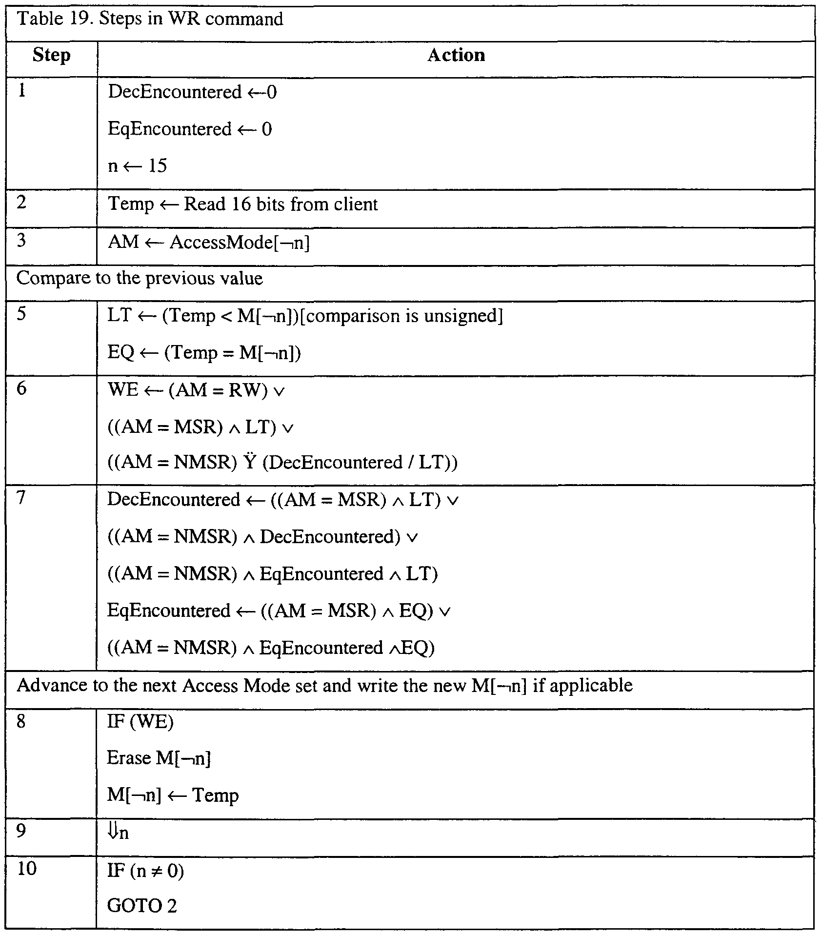


Claims
Priority Applications (7)
| Application Number | Priority Date | Filing Date | Title |
|---|---|---|---|
| AU2001231441A AU2001231441B2 (en) | 2000-02-15 | 2001-02-15 | Consumable authentication protocol and system |
| DE60120117T DE60120117D1 (en) | 2000-02-15 | 2001-02-15 | DEVICE AND PROTOCOL FOR AUTHENTICATING A CONSUMER OBJECT |
| EP01903528A EP1260053B1 (en) | 2000-02-15 | 2001-02-15 | Consumable authentication protocol and system |
| US10/203,560 US7197642B2 (en) | 2000-02-15 | 2001-02-15 | Consumable authentication protocol and system |
| CA2400220A CA2400220C (en) | 2000-02-15 | 2001-02-15 | Consumable authentication protocol and system |
| US11/706,329 US7757084B2 (en) | 2000-02-15 | 2007-02-15 | Method of validating consumable authentication chip |
| US12/832,950 US7941661B2 (en) | 2000-02-15 | 2010-07-08 | Method of testing validity of authentication IC |
Applications Claiming Priority (2)
| Application Number | Priority Date | Filing Date | Title |
|---|---|---|---|
| US09/505,147 | 2000-02-15 | ||
| US09/505,147 US6816968B1 (en) | 1998-07-10 | 2000-02-15 | Consumable authentication protocol and system |
Related Parent Applications (1)
| Application Number | Title | Priority Date | Filing Date |
|---|---|---|---|
| US09/505,147 Continuation US6816968B1 (en) | 1998-07-10 | 2000-02-15 | Consumable authentication protocol and system |
Related Child Applications (2)
| Application Number | Title | Priority Date | Filing Date |
|---|---|---|---|
| US10203560 A-371-Of-International | 2001-02-15 | ||
| US11/706,329 Continuation US7757084B2 (en) | 2000-02-15 | 2007-02-15 | Method of validating consumable authentication chip |
Publications (1)
| Publication Number | Publication Date |
|---|---|
| WO2001061917A1 true WO2001061917A1 (en) | 2001-08-23 |
Family
ID=24009208
Family Applications (1)
| Application Number | Title | Priority Date | Filing Date |
|---|---|---|---|
| PCT/AU2001/000139 WO2001061917A1 (en) | 2000-02-15 | 2001-02-15 | Consumable authentication protocol and system |
Country Status (8)
| Country | Link |
|---|---|
| US (3) | US7197642B2 (en) |
| EP (1) | EP1260053B1 (en) |
| AT (1) | ATE328420T1 (en) |
| AU (1) | AU2001231441B2 (en) |
| CA (1) | CA2400220C (en) |
| DE (1) | DE60120117D1 (en) |
| SG (1) | SG127734A1 (en) |
| WO (1) | WO2001061917A1 (en) |
Cited By (5)
| Publication number | Priority date | Publication date | Assignee | Title |
|---|---|---|---|---|
| US7097107B1 (en) | 2003-04-09 | 2006-08-29 | Mobile-Mind, Inc. | Pseudo-random number sequence file for an integrated circuit card |
| EP2495678A3 (en) * | 2011-03-04 | 2014-01-08 | Broadcom Corporation | Enforcing software updates in an electronic device |
| US9098216B2 (en) | 2012-04-25 | 2015-08-04 | Hewlett-Packard Development Company, L.P. | Printer functionality enablement |
| US10592289B2 (en) | 2014-10-31 | 2020-03-17 | Hewlett-Packard Development Company, L.P. | Providing auxiliary services or functionality on an apparatus |
| US11022421B2 (en) | 2016-01-20 | 2021-06-01 | Lucent Medical Systems, Inc. | Low-frequency electromagnetic tracking |
Families Citing this family (70)
| Publication number | Priority date | Publication date | Assignee | Title |
|---|---|---|---|---|
| GB0004178D0 (en) * | 2000-02-22 | 2000-04-12 | Nokia Networks Oy | Integrity check in a communication system |
| US8156223B2 (en) * | 2001-03-20 | 2012-04-10 | Microsoft Corporation | Distribution of binary executables and content from peer locations/machines |
| FR2826811B1 (en) * | 2001-06-27 | 2003-11-07 | France Telecom | CRYPTOGRAPHIC AUTHENTICATION PROCESS |
| US20030035646A1 (en) * | 2001-08-20 | 2003-02-20 | Vat 19, Llc | Digital video device having a verification code thereon and method of generating a verification code |
| US7599976B1 (en) * | 2002-11-13 | 2009-10-06 | Metrowerks Corporation | System and method for cryptographic key generation |
| EP1439697A1 (en) * | 2003-01-20 | 2004-07-21 | Thomson Licensing S.A. | Digital broadcast data reception system with digital master terminal ,and at least one digital slave terminal |
| JP2004226605A (en) * | 2003-01-22 | 2004-08-12 | Fuji Photo Film Co Ltd | Image forming device |
| US20050071866A1 (en) * | 2003-01-30 | 2005-03-31 | Ali Louzir | System for receiving broadcast digital data comprising a master digital terminal, and at least one slave digital terminal |
| US8165297B2 (en) | 2003-11-21 | 2012-04-24 | Finisar Corporation | Transceiver with controller for authentication |
| EP1740418B1 (en) * | 2004-04-29 | 2012-06-13 | Bayerische Motoren Werke Aktiengesellschaft | Authentication of a vehicle-external device |
| JP2005336911A (en) * | 2004-05-28 | 2005-12-08 | Mitsubishi Electric Corp | Vehicle control system and on-vehicle controller and portable machine used in it |
| US8099791B1 (en) | 2004-06-25 | 2012-01-17 | Lexmark International, Inc. | Method of authenticating a consumable in an imaging device |
| US7221878B2 (en) * | 2005-02-18 | 2007-05-22 | Hewlett-Packard Development Company, L.P. | Allowing image formation using consumable item where code of consumable item is identical to code of image-formation device |
| US9794247B2 (en) * | 2006-08-22 | 2017-10-17 | Stmicroelectronics, Inc. | Method to prevent cloning of electronic components using public key infrastructure secure hardware device |
| KR100873790B1 (en) * | 2006-12-18 | 2008-12-15 | 주식회사 케이티 | Authentication system and method for low cost electronics |
| US8762714B2 (en) * | 2007-04-24 | 2014-06-24 | Finisar Corporation | Protecting against counterfeit electronics devices |
| EP2421221B1 (en) * | 2007-06-11 | 2013-10-23 | FTS Computertechnik GmbH | Method and architecture for securing real time data |
| US7962304B2 (en) * | 2007-08-02 | 2011-06-14 | Lsi Corporation | Device for thorough testing of secure electronic components |
| US9148286B2 (en) * | 2007-10-15 | 2015-09-29 | Finisar Corporation | Protecting against counterfeit electronic devices |
| WO2009059331A2 (en) * | 2007-11-02 | 2009-05-07 | Finisar Corporation | Anticounterfeiting means for optical communication components |
| US8819423B2 (en) * | 2007-11-27 | 2014-08-26 | Finisar Corporation | Optical transceiver with vendor authentication |
| US8312269B2 (en) * | 2007-11-28 | 2012-11-13 | Hitachi Global Storage Technologies Netherlands, B.V. | Challenge and response access control providing data security in data storage devices |
| FR2926381A1 (en) * | 2008-01-11 | 2009-07-17 | Sagem Securite Sa | METHOD OF SECURE TRANSFER OF DATA |
| DE102008008237B4 (en) | 2008-02-08 | 2021-06-02 | Volkswagen Ag | Method and system for detecting the rotational movement of a vehicle wheel |
| US8001379B2 (en) * | 2008-03-26 | 2011-08-16 | Mformation Technologies Inc. | Credential generation system and method for communications devices and device management servers |
| US9003197B2 (en) * | 2008-03-27 | 2015-04-07 | General Instrument Corporation | Methods, apparatus and system for authenticating a programmable hardware device and for authenticating commands received in the programmable hardware device from a secure processor |
| EP2382536B1 (en) * | 2009-01-29 | 2018-04-25 | Fortress Applications Ltd. | System and methods for encryption with authentication integrity |
| US8789746B2 (en) * | 2009-01-31 | 2014-07-29 | Solexir Technology Inc. | Product authentication using integrated circuits |
| US8234715B2 (en) * | 2009-04-13 | 2012-07-31 | Netflix, Inc. | Activating streaming video in a blu-ray disc player |
| US8521852B2 (en) * | 2009-12-28 | 2013-08-27 | The Directv Group, Inc. | Method and system for registering a client device in a multi-room digital video recording system |
| DE102010002472A1 (en) * | 2010-03-01 | 2011-09-01 | Robert Bosch Gmbh | Method for verifying a memory block of a non-volatile memory |
| MY150351A (en) * | 2010-07-06 | 2013-12-31 | Mimos Berhad | A method for rootkit resistance based on a trusted chip |
| CN101916346A (en) * | 2010-08-16 | 2010-12-15 | 鸿富锦精密工业(深圳)有限公司 | Electronic device capable of preventing piracy and anti-piracy method thereof |
| US8938624B2 (en) * | 2010-09-15 | 2015-01-20 | Lsi Corporation | Encryption key destruction for secure data erasure |
| CN102136079B (en) * | 2011-03-07 | 2014-08-20 | 中兴通讯股份有限公司 | Dynamic authentication method between reader and tag card and implementing device thereof |
| CN102447955B (en) * | 2011-12-27 | 2015-04-15 | 深圳国微技术有限公司 | Condition access chip of digital television and realization method of condition access |
| US10756558B2 (en) * | 2012-03-29 | 2020-08-25 | Integrated Device Technology, Inc. | Establishing trusted relationships for multimodal wireless power transfer |
| US8776195B1 (en) * | 2012-03-30 | 2014-07-08 | Emc Corporation | Common data format in knowledge-based authentication |
| US9002812B2 (en) * | 2012-04-01 | 2015-04-07 | Microsoft Technology Licensing, Llc | Checksum and hashing operations resilient to malicious input data |
| US8912816B2 (en) | 2012-11-12 | 2014-12-16 | Chaologix, Inc. | Charge distribution control for secure systems |
| US8912814B2 (en) | 2012-11-12 | 2014-12-16 | Chaologix, Inc. | Clocked charge domain logic |
| US9047192B2 (en) * | 2012-12-21 | 2015-06-02 | Advanced Micro Devices, Inc. | Signature-based store checking buffer |
| JP6976682B2 (en) * | 2013-03-15 | 2021-12-08 | ビデリ、インコーポレイテッドVideri Inc. | Systems and methods for displaying, distributing, viewing and controlling digital art and forming images |
| TWI620094B (en) * | 2013-05-31 | 2018-04-01 | 凱爾拉吉克斯股份有限公司 | Charge distribution control system, crypto system and method of protecting against side channel attack by operating the same |
| US9953166B2 (en) * | 2013-07-04 | 2018-04-24 | Microsemi SoC Corporation | Method for securely booting target processor in target system using a secure root of trust to verify a returned message authentication code recreated by the target processor |
| US20150242620A1 (en) | 2014-02-27 | 2015-08-27 | Microsemi SoC Corporation | Methods for controlling the use of intellectual property in individual integrated circuit devices |
| US10114369B2 (en) | 2014-06-24 | 2018-10-30 | Microsemi SoC Corporation | Identifying integrated circuit origin using tooling signature |
| DE102014212488B4 (en) * | 2014-06-27 | 2016-02-18 | Siemens Aktiengesellschaft | Securely providing a replica pseudorandom noise code to a receiver unit |
| US10353638B2 (en) | 2014-11-18 | 2019-07-16 | Microsemi SoC Corporation | Security method and apparatus to prevent replay of external memory data to integrated circuits having only one-time programmable non-volatile memory |
| US9940486B2 (en) * | 2015-02-23 | 2018-04-10 | Cisco Technology, Inc. | Detection of hardware tampering |
| US10892889B2 (en) * | 2015-04-07 | 2021-01-12 | Coleridge Enterprises Llc | Systems and methods for an enhanced XOR cipher through extensions |
| CZ2015473A3 (en) * | 2015-07-07 | 2017-02-08 | Aducid S.R.O. | The method of authentication security in electronic communication |
| KR101838511B1 (en) * | 2016-05-17 | 2018-03-14 | 현대자동차주식회사 | Method of providing security for controller using encryption and appratus for implementing the same |
| US10833877B2 (en) * | 2017-10-12 | 2020-11-10 | Canon Kabushiki Kaisha | Method of authenticating authentication-target apparatus by authentication apparatus, authentication apparatus, authentication- target apparatus, and image forming apparatus |
| FR3076923A1 (en) * | 2018-01-16 | 2019-07-19 | Stmicroelectronics (Rousset) Sas | METHOD AND AUTHENTICATION CIRCUIT |
| WO2019191579A1 (en) * | 2018-03-30 | 2019-10-03 | Walmart Apollo, Llc | System and methods for recording codes in a distributed environment |
| CN110580420B (en) | 2018-06-11 | 2023-03-28 | 阿里巴巴集团控股有限公司 | Data processing method based on integrated chip, computer equipment and storage medium |
| CN109714163B (en) * | 2019-01-30 | 2021-12-14 | 江永林 | Chip sequence number coding method and system, storage medium and terminal |
| US10878950B1 (en) * | 2019-08-09 | 2020-12-29 | HealthBlock, Inc. | Verifying data accuracy in privacy-preserving computations |
| US10635837B1 (en) | 2019-04-30 | 2020-04-28 | HealthBlock, Inc. | Dynamic data protection |
| FR3098949B1 (en) | 2019-07-15 | 2023-10-06 | St Microelectronics Rousset | One-way function |
| CN110505205B (en) * | 2019-07-18 | 2021-04-23 | 华信永道(北京)科技股份有限公司 | Cloud platform encryption and decryption service access method and access system |
| US11126752B2 (en) * | 2019-09-04 | 2021-09-21 | Fresenius Medical Care Holdings, Inc. | Authentication of medical device computing systems by using metadata signature |
| US11804955B1 (en) | 2019-09-13 | 2023-10-31 | Chol, Inc. | Method and system for modulated waveform encryption |
| WO2022066142A1 (en) * | 2020-09-22 | 2022-03-31 | Google Llc | Secure provisioning with hardware verification |
| WO2022164441A1 (en) * | 2021-01-29 | 2022-08-04 | Hewlett-Packard Development Company, L.P. | Generating a response to an attestation challenge using a private key |
| CN113138548B (en) * | 2021-04-22 | 2022-11-01 | 珠海奔图电子有限公司 | Image forming apparatus, consumable chip, consumable, and communication method |
| US20230153422A1 (en) * | 2021-11-18 | 2023-05-18 | Rocksavage Technology, Inc. | Method, System and Apparatus for Detecting Malicious Modifications to Semiconductor Devices |
| FR3138553A1 (en) * | 2022-07-27 | 2024-02-02 | La Française Des Jeux | Method, device and computer program for electronic printing |
| CN115774182B (en) * | 2022-12-05 | 2023-10-13 | 安测半导体技术(义乌)有限公司 | Chip testing method and device based on ATE platform |
Citations (3)
| Publication number | Priority date | Publication date | Assignee | Title |
|---|---|---|---|---|
| DE19716111A1 (en) * | 1997-04-17 | 1998-10-22 | Giesecke & Devrient Gmbh | Procedure for mutual authentication of two units |
| JPH118618A (en) * | 1997-06-17 | 1999-01-12 | Toshiba Corp | Device authentication method, system and authentication system |
| EP0915590A2 (en) * | 1997-11-10 | 1999-05-12 | Unwired Planet, Inc. | Method and system for secure lightweight transactions in wireless data networks |
Family Cites Families (30)
| Publication number | Priority date | Publication date | Assignee | Title |
|---|---|---|---|---|
| US3816765A (en) * | 1972-06-27 | 1974-06-11 | Rca Corp | Digital interface circuit for a random noise generator |
| US4667192A (en) | 1983-05-24 | 1987-05-19 | The Johns Hopkins University | Method and apparatus for bus arbitration using a pseudo-random sequence |
| US4736423A (en) | 1985-04-30 | 1988-04-05 | International Business Machines Corporation | Technique for reducing RSA Crypto variable storage |
| US4799061A (en) | 1985-11-18 | 1989-01-17 | International Business Machines Corporation | Secure component authentication system |
| US4799059A (en) * | 1986-03-14 | 1989-01-17 | Enscan, Inc. | Automatic/remote RF instrument monitoring system |
| US5036461A (en) | 1990-05-16 | 1991-07-30 | Elliott John C | Two-way authentication system between user's smart card and issuer-specific plug-in application modules in multi-issued transaction device |
| EP0460538B1 (en) | 1990-06-01 | 1998-03-04 | Kabushiki Kaisha Toshiba | Cryptographic communication method and cryptographic communication device |
| US5196840A (en) | 1990-11-05 | 1993-03-23 | International Business Machines Corporation | Secure communications system for remotely located computers |
| JP2671649B2 (en) | 1991-07-08 | 1997-10-29 | 三菱電機株式会社 | Authentication method |
| US5499294A (en) * | 1993-11-24 | 1996-03-12 | The United States Of America As Represented By The Administrator Of The National Aeronautics And Space Administration | Digital camera with apparatus for authentication of images produced from an image file |
| US5515441A (en) | 1994-05-12 | 1996-05-07 | At&T Corp. | Secure communication method and apparatus |
| US5506905A (en) | 1994-06-10 | 1996-04-09 | Delco Electronics Corp. | Authentication method for keyless entry system |
| US5619571A (en) | 1995-06-01 | 1997-04-08 | Sandstrom; Brent B. | Method for securely storing electronic records |
| JP3541522B2 (en) | 1995-10-09 | 2004-07-14 | 松下電器産業株式会社 | Communication protection system and equipment between devices |
| US5633932A (en) * | 1995-12-19 | 1997-05-27 | Intel Corporation | Apparatus and method for preventing disclosure through user-authentication at a printing node |
| US6073236A (en) | 1996-06-28 | 2000-06-06 | Sony Corporation | Authentication method, communication method, and information processing apparatus |
| US5787367A (en) * | 1996-07-03 | 1998-07-28 | Chrysler Corporation | Flash reprogramming security for vehicle computer |
| EP0831344B1 (en) * | 1996-09-20 | 2003-02-26 | Infineon Technologies AG | Arrangement of two integrated optics lightguides on the upper surface of a substrate |
| JP3163996B2 (en) | 1996-11-15 | 2001-05-08 | 日本電気株式会社 | Method for manufacturing semiconductor device |
| US5757388A (en) * | 1996-12-16 | 1998-05-26 | Eastman Kodak Company | Electronic camera and integral ink jet printer |
| US6192473B1 (en) | 1996-12-24 | 2001-02-20 | Pitney Bowes Inc. | System and method for mutual authentication and secure communications between a postage security device and a meter server |
| AUPO799197A0 (en) | 1997-07-15 | 1997-08-07 | Silverbrook Research Pty Ltd | Image processing method and apparatus (ART01) |
| GB9709135D0 (en) | 1997-05-02 | 1997-06-25 | Certicom Corp | Two way authentication protocol |
| JPH10340486A (en) | 1997-06-06 | 1998-12-22 | Toshiba Corp | Optical disk, master disk manufacturing device of the same and manufacture of the same |
| EP1082710A1 (en) * | 1998-06-05 | 2001-03-14 | Landis & Gyr Communications S.A. | Preloaded ic-card and method for authenticating the same |
| US6816968B1 (en) * | 1998-07-10 | 2004-11-09 | Silverbrook Research Pty Ltd | Consumable authentication protocol and system |
| JP2002529008A (en) | 1998-10-23 | 2002-09-03 | エル3 コミュニケーションズ コーポレイション | Apparatus and method for managing key material in disparate cryptographic assets |
| US6389533B1 (en) | 1999-02-05 | 2002-05-14 | Intel Corporation | Anonymity server |
| US6529487B1 (en) | 1999-07-09 | 2003-03-04 | Qualcomm Incorporated | Method and apparatus for securely transmitting distributed RAND for use in mobile station authentication |
| US7685423B1 (en) | 2000-02-15 | 2010-03-23 | Silverbrook Research Pty Ltd | Validation protocol and system |
-
2001
- 2001-02-15 US US10/203,560 patent/US7197642B2/en not_active Expired - Fee Related
- 2001-02-15 CA CA2400220A patent/CA2400220C/en not_active Expired - Fee Related
- 2001-02-15 DE DE60120117T patent/DE60120117D1/en not_active Expired - Lifetime
- 2001-02-15 WO PCT/AU2001/000139 patent/WO2001061917A1/en active IP Right Grant
- 2001-02-15 AU AU2001231441A patent/AU2001231441B2/en not_active Ceased
- 2001-02-15 SG SG200404566A patent/SG127734A1/en unknown
- 2001-02-15 AT AT01903528T patent/ATE328420T1/en not_active IP Right Cessation
- 2001-02-15 EP EP01903528A patent/EP1260053B1/en not_active Expired - Lifetime
-
2007
- 2007-02-15 US US11/706,329 patent/US7757084B2/en not_active Expired - Fee Related
-
2010
- 2010-07-08 US US12/832,950 patent/US7941661B2/en not_active Expired - Fee Related
Patent Citations (3)
| Publication number | Priority date | Publication date | Assignee | Title |
|---|---|---|---|---|
| DE19716111A1 (en) * | 1997-04-17 | 1998-10-22 | Giesecke & Devrient Gmbh | Procedure for mutual authentication of two units |
| JPH118618A (en) * | 1997-06-17 | 1999-01-12 | Toshiba Corp | Device authentication method, system and authentication system |
| EP0915590A2 (en) * | 1997-11-10 | 1999-05-12 | Unwired Planet, Inc. | Method and system for secure lightweight transactions in wireless data networks |
Non-Patent Citations (2)
| Title |
|---|
| DATABASE WPI Derwent World Patents Index; Class W01, AN 1998-558382, XP002957569 * |
| PATENT ABSTRACTS OF JAPAN * |
Cited By (6)
| Publication number | Priority date | Publication date | Assignee | Title |
|---|---|---|---|---|
| US7097107B1 (en) | 2003-04-09 | 2006-08-29 | Mobile-Mind, Inc. | Pseudo-random number sequence file for an integrated circuit card |
| EP2495678A3 (en) * | 2011-03-04 | 2014-01-08 | Broadcom Corporation | Enforcing software updates in an electronic device |
| US8954722B2 (en) | 2011-03-04 | 2015-02-10 | Broadcom Corporation | Enforcing software updates in an electronic device |
| US9098216B2 (en) | 2012-04-25 | 2015-08-04 | Hewlett-Packard Development Company, L.P. | Printer functionality enablement |
| US10592289B2 (en) | 2014-10-31 | 2020-03-17 | Hewlett-Packard Development Company, L.P. | Providing auxiliary services or functionality on an apparatus |
| US11022421B2 (en) | 2016-01-20 | 2021-06-01 | Lucent Medical Systems, Inc. | Low-frequency electromagnetic tracking |
Also Published As
| Publication number | Publication date |
|---|---|
| EP1260053A1 (en) | 2002-11-27 |
| SG127734A1 (en) | 2006-12-29 |
| DE60120117D1 (en) | 2006-07-06 |
| US20070143623A1 (en) | 2007-06-21 |
| CA2400220A1 (en) | 2001-08-23 |
| US7757084B2 (en) | 2010-07-13 |
| CA2400220C (en) | 2013-07-30 |
| EP1260053A4 (en) | 2004-06-16 |
| AU2001231441B2 (en) | 2004-02-05 |
| US7197642B2 (en) | 2007-03-27 |
| US20030172268A1 (en) | 2003-09-11 |
| EP1260053B1 (en) | 2006-05-31 |
| ATE328420T1 (en) | 2006-06-15 |
| AU3144101A (en) | 2001-08-27 |
| US7941661B2 (en) | 2011-05-10 |
| US20100275063A1 (en) | 2010-10-28 |
Similar Documents
| Publication | Publication Date | Title |
|---|---|---|
| AU2001231443B2 (en) | Validation protocol and system | |
| AU2001231441B2 (en) | Consumable authentication protocol and system | |
| AU2001231442B2 (en) | Unauthorised modification of values stored in flash memory | |
| US6816968B1 (en) | Consumable authentication protocol and system | |
| AU2001231442A1 (en) | Unauthorised modification of values stored in flash memory | |
| AU2001231443A1 (en) | Validation protocol and system | |
| AU2004201740B2 (en) | Validation chip | |
| AU2004201742B2 (en) | Consumables validation chip | |
| AU2004226966B2 (en) | Validating an authentication chip using a secret key | |
| AU2005200945B2 (en) | Integrated Circuit For Authenticating an Object | |
| AU2004205292B2 (en) | A system for authenticating an object | |
| AU2006252277B2 (en) | An Apparatus for Validating a Device | |
| AU2006252272B2 (en) | An apparatus for validating a device using first and second keys | |
| AU2001231441A1 (en) | Consumable authentication protocol and system |
Legal Events
| Date | Code | Title | Description |
|---|---|---|---|
| AK | Designated states |
Kind code of ref document: A1 Designated state(s): AE AG AL AM AT AU AZ BA BB BG BR BY BZ CA CH CN CR CU CZ DE DK DM DZ EE ES FI GB GD GE GH GM HR HU ID IL IN IS JP KE KG KP KR KZ LC LK LR LS LT LU LV MA MD MG MK MN MW MX MZ NO NZ PL PT RO RU SD SE SG SI SK SL TJ TM TR TT TZ UA UG US UZ VN YU ZA ZW |
|
| AL | Designated countries for regional patents |
Kind code of ref document: A1 Designated state(s): GH GM KE LS MW MZ SD SL SZ TZ UG ZW AM AZ BY KG KZ MD RU TJ TM AT BE CH CY DE DK ES FI FR GB GR IE IT LU MC NL PT SE TR BF BJ CF CG CI CM GA GN GW ML MR NE SN TD TG |
|
| DFPE | Request for preliminary examination filed prior to expiration of 19th month from priority date (pct application filed before 20040101) | ||
| 121 | Ep: the epo has been informed by wipo that ep was designated in this application | ||
| WWE | Wipo information: entry into national phase |
Ref document number: 10203560 Country of ref document: US |
|
| WWE | Wipo information: entry into national phase |
Ref document number: 2001231441 Country of ref document: AU |
|
| WWE | Wipo information: entry into national phase |
Ref document number: 2400220 Country of ref document: CA |
|
| WWE | Wipo information: entry into national phase |
Ref document number: 2001903528 Country of ref document: EP |
|
| WWP | Wipo information: published in national office |
Ref document number: 2001903528 Country of ref document: EP |
|
| REG | Reference to national code |
Ref country code: DE Ref legal event code: 8642 Ref country code: DE Ref legal event code: 8642 |
|
| WWG | Wipo information: grant in national office |
Ref document number: 2001231441 Country of ref document: AU |
|
| NENP | Non-entry into the national phase |
Ref country code: JP |
|
| WWG | Wipo information: grant in national office |
Ref document number: 2001903528 Country of ref document: EP |