WO2004021463A2 - Buffer layers for organic electroluminescent devices and methods of manufacture and use - Google Patents
Buffer layers for organic electroluminescent devices and methods of manufacture and use Download PDFInfo
- Publication number
- WO2004021463A2 WO2004021463A2 PCT/US2003/014466 US0314466W WO2004021463A2 WO 2004021463 A2 WO2004021463 A2 WO 2004021463A2 US 0314466 W US0314466 W US 0314466W WO 2004021463 A2 WO2004021463 A2 WO 2004021463A2
- Authority
- WO
- WIPO (PCT)
- Prior art keywords
- buffer layer
- electroluminescent device
- layer
- hole transport
- triarylamine
- Prior art date
Links
Classifications
-
- H—ELECTRICITY
- H10—SEMICONDUCTOR DEVICES; ELECTRIC SOLID-STATE DEVICES NOT OTHERWISE PROVIDED FOR
- H10K—ORGANIC ELECTRIC SOLID-STATE DEVICES
- H10K85/00—Organic materials used in the body or electrodes of devices covered by this subclass
- H10K85/10—Organic polymers or oligomers
- H10K85/111—Organic polymers or oligomers comprising aromatic, heteroaromatic, or aryl chains, e.g. polyaniline, polyphenylene or polyphenylene vinylene
-
- H—ELECTRICITY
- H05—ELECTRIC TECHNIQUES NOT OTHERWISE PROVIDED FOR
- H05B—ELECTRIC HEATING; ELECTRIC LIGHT SOURCES NOT OTHERWISE PROVIDED FOR; CIRCUIT ARRANGEMENTS FOR ELECTRIC LIGHT SOURCES, IN GENERAL
- H05B33/00—Electroluminescent light sources
- H05B33/12—Light sources with substantially two-dimensional radiating surfaces
- H05B33/22—Light sources with substantially two-dimensional radiating surfaces characterised by the chemical or physical composition or the arrangement of auxiliary dielectric or reflective layers
-
- H—ELECTRICITY
- H05—ELECTRIC TECHNIQUES NOT OTHERWISE PROVIDED FOR
- H05B—ELECTRIC HEATING; ELECTRIC LIGHT SOURCES NOT OTHERWISE PROVIDED FOR; CIRCUIT ARRANGEMENTS FOR ELECTRIC LIGHT SOURCES, IN GENERAL
- H05B33/00—Electroluminescent light sources
- H05B33/10—Apparatus or processes specially adapted to the manufacture of electroluminescent light sources
-
- H—ELECTRICITY
- H10—SEMICONDUCTOR DEVICES; ELECTRIC SOLID-STATE DEVICES NOT OTHERWISE PROVIDED FOR
- H10K—ORGANIC ELECTRIC SOLID-STATE DEVICES
- H10K10/00—Organic devices specially adapted for rectifying, amplifying, oscillating or switching; Organic capacitors or resistors having a potential-jump barrier or a surface barrier
-
- H—ELECTRICITY
- H10—SEMICONDUCTOR DEVICES; ELECTRIC SOLID-STATE DEVICES NOT OTHERWISE PROVIDED FOR
- H10K—ORGANIC ELECTRIC SOLID-STATE DEVICES
- H10K50/00—Organic light-emitting devices
- H10K50/10—OLEDs or polymer light-emitting diodes [PLED]
- H10K50/11—OLEDs or polymer light-emitting diodes [PLED] characterised by the electroluminescent [EL] layers
- H10K50/125—OLEDs or polymer light-emitting diodes [PLED] characterised by the electroluminescent [EL] layers specially adapted for multicolour light emission, e.g. for emitting white light
-
- H—ELECTRICITY
- H10—SEMICONDUCTOR DEVICES; ELECTRIC SOLID-STATE DEVICES NOT OTHERWISE PROVIDED FOR
- H10K—ORGANIC ELECTRIC SOLID-STATE DEVICES
- H10K50/00—Organic light-emitting devices
- H10K50/10—OLEDs or polymer light-emitting diodes [PLED]
- H10K50/14—Carrier transporting layers
- H10K50/15—Hole transporting layers
- H10K50/155—Hole transporting layers comprising dopants
-
- H—ELECTRICITY
- H10—SEMICONDUCTOR DEVICES; ELECTRIC SOLID-STATE DEVICES NOT OTHERWISE PROVIDED FOR
- H10K—ORGANIC ELECTRIC SOLID-STATE DEVICES
- H10K50/00—Organic light-emitting devices
- H10K50/10—OLEDs or polymer light-emitting diodes [PLED]
- H10K50/17—Carrier injection layers
-
- H—ELECTRICITY
- H10—SEMICONDUCTOR DEVICES; ELECTRIC SOLID-STATE DEVICES NOT OTHERWISE PROVIDED FOR
- H10K—ORGANIC ELECTRIC SOLID-STATE DEVICES
- H10K50/00—Organic light-emitting devices
- H10K50/80—Constructional details
- H10K50/85—Arrangements for extracting light from the devices
- H10K50/854—Arrangements for extracting light from the devices comprising scattering means
-
- H—ELECTRICITY
- H10—SEMICONDUCTOR DEVICES; ELECTRIC SOLID-STATE DEVICES NOT OTHERWISE PROVIDED FOR
- H10K—ORGANIC ELECTRIC SOLID-STATE DEVICES
- H10K85/00—Organic materials used in the body or electrodes of devices covered by this subclass
- H10K85/10—Organic polymers or oligomers
- H10K85/151—Copolymers
-
- H—ELECTRICITY
- H10—SEMICONDUCTOR DEVICES; ELECTRIC SOLID-STATE DEVICES NOT OTHERWISE PROVIDED FOR
- H10K—ORGANIC ELECTRIC SOLID-STATE DEVICES
- H10K99/00—Subject matter not provided for in other groups of this subclass
-
- H—ELECTRICITY
- H10—SEMICONDUCTOR DEVICES; ELECTRIC SOLID-STATE DEVICES NOT OTHERWISE PROVIDED FOR
- H10K—ORGANIC ELECTRIC SOLID-STATE DEVICES
- H10K71/00—Manufacture or treatment specially adapted for the organic devices covered by this subclass
- H10K71/10—Deposition of organic active material
- H10K71/18—Deposition of organic active material using non-liquid printing techniques, e.g. thermal transfer printing from a donor sheet
-
- H—ELECTRICITY
- H10—SEMICONDUCTOR DEVICES; ELECTRIC SOLID-STATE DEVICES NOT OTHERWISE PROVIDED FOR
- H10K—ORGANIC ELECTRIC SOLID-STATE DEVICES
- H10K85/00—Organic materials used in the body or electrodes of devices covered by this subclass
- H10K85/10—Organic polymers or oligomers
- H10K85/141—Organic polymers or oligomers comprising aliphatic or olefinic chains, e.g. poly N-vinylcarbazol, PVC or PTFE
-
- H—ELECTRICITY
- H10—SEMICONDUCTOR DEVICES; ELECTRIC SOLID-STATE DEVICES NOT OTHERWISE PROVIDED FOR
- H10K—ORGANIC ELECTRIC SOLID-STATE DEVICES
- H10K85/00—Organic materials used in the body or electrodes of devices covered by this subclass
- H10K85/60—Organic compounds having low molecular weight
- H10K85/611—Charge transfer complexes
-
- H—ELECTRICITY
- H10—SEMICONDUCTOR DEVICES; ELECTRIC SOLID-STATE DEVICES NOT OTHERWISE PROVIDED FOR
- H10K—ORGANIC ELECTRIC SOLID-STATE DEVICES
- H10K85/00—Organic materials used in the body or electrodes of devices covered by this subclass
- H10K85/60—Organic compounds having low molecular weight
- H10K85/615—Polycyclic condensed aromatic hydrocarbons, e.g. anthracene
-
- H—ELECTRICITY
- H10—SEMICONDUCTOR DEVICES; ELECTRIC SOLID-STATE DEVICES NOT OTHERWISE PROVIDED FOR
- H10K—ORGANIC ELECTRIC SOLID-STATE DEVICES
- H10K85/00—Organic materials used in the body or electrodes of devices covered by this subclass
- H10K85/60—Organic compounds having low molecular weight
- H10K85/631—Amine compounds having at least two aryl rest on at least one amine-nitrogen atom, e.g. triphenylamine
-
- H—ELECTRICITY
- H10—SEMICONDUCTOR DEVICES; ELECTRIC SOLID-STATE DEVICES NOT OTHERWISE PROVIDED FOR
- H10K—ORGANIC ELECTRIC SOLID-STATE DEVICES
- H10K85/00—Organic materials used in the body or electrodes of devices covered by this subclass
- H10K85/60—Organic compounds having low molecular weight
- H10K85/649—Aromatic compounds comprising a hetero atom
Definitions
- Organic electroluminescent devices include layers of organic materials, at least one of which can conduct a charge.
- organic electroluminescent devices include organic light emitting diodes (OLEDs).
- OEL devices organic light emitting diodes
- OEL devices have potential use in applications such as, for example, lighting applications, backlighting of graphics, pixelated displays, and large emissive graphics.
- OEL devices typically include an organic light emitter layer and optionally one or more charge transport layers, all of which are sandwiched between two electrodes: a cathode and an anode.
- Charge carriers, electrons and holes, are injected from the cathode and anode, respectively.
- Electrons are negatively charged atomic particles and holes are vacant electron energy states that behave as though they are positively charged particles. The charge carriers migrate to the emitter layer, where they combine to emit light.
- This basic OEL device structure can be modified to improve or enhance one or more electrical, chemical, or physical properties of the device. Such modification can include the addition or modification of one or more of the basic layers.
- the present invention relates to organic electroluminescent devices, articles containing the organic electroluminescent devices, and methods of making and using the organic electroluminescent devices and articles.
- One embodiment is an electroluminescent device having multiple layers including, but not limited to, an electrode, an emission layer, and a buffer layer.
- the emission layer ' includes a light emitting material.
- the buffer layer is disposed between and in electrical communication with the electrode and the emission layer and includes a triarylamine hole transport material and an electron acceptor material.
- the buffer layer optionally includes one or more of a) a polymeric binder, b) a color converting material, and c) light scattering particles.
- Another embodiment is a method of making an electroluminescent device.
- the method includes forming an electrode, coating a buffer layer from solution over the electrode, and disposing an emission layer over the buffer layer.
- the electrode, buffer layer, and emission layer are in electrical communication.
- the emission layer includes a light emitting material.
- the buffer layer includes a triarylamine hole transport material and an electron acceptor material.
- the buffer layer includes one or more of a) a polymeric binder, b) a color converting material, and c) light scattering particles.
- an electroluminescent device having multiple layers including, but not limited to, an electrode, an emission layer, and a buffer layer.
- the emission layer includes a light emitting material.
- the buffer layer is disposed between and in electrical communication with the electrode and the emission layer.
- the buffer layer includes (a) a polymeric hole transport material having triarylamine moieties and (b) an electron acceptor material.
- the buffer layer includes one or more of a) a color converting material, and b) light scattering particles.
- Another embodiment is a method of making an electroluminescent device.
- the method includes forming an electrode, coating a buffer layer from solution over the electrode, and disposing an emission layer over the buffer layer.
- the electrode, buffer layer, and emission layer are in electrical communication.
- the emission layer includes a light emitting material.
- the buffer layer includes (a) a polymeric hole transport material having triarylamine moieties and (b) an electron acceptor material.
- the buffer layer includes one or more of a) a color converting material, and b) light scattering particles.
- Figure 1 is a schematic side view of an organic electroluminescent display construction
- Figure 2 is a schematic side view of a first embodiment of an electroluminescent device, according to the present invention.
- Figure 3 is a schematic side view of a second embodiment of an electroluminescent device, according to the present invention.
- Figure 4 is a schematic side view of a third embodiment of an electroluminescent device, according to the present invention.
- FIG. 5 is a schematic side view of an organic electroluminescent display according to the present invention. While the invention is amenable to various modifications and alternative forms, specifics thereof have been shown by way of example in the drawings and will be described in detail. It should be understood, however, that the intention is not to limit the invention to the particular embodiments described. On the contrary, the intention is to cover all modifications, equivalents, and alternatives falling within the spirit and scope of the invention.
- the present invention is believed to be applicable to electroluminescent devices, articles containing the electroluminescent devices, and methods of making and using the electroluminescent devices and articles.
- the present invention is directed to organic electroluminescent devices containing a buffer layer with a triarylamine material and an electron acceptor material, articles containing the organic electroluminescent devices, and methods of making and using the organic electroluminescent devices and articles.
- Pixelated and non-pixelated electroluminescent displays, backlights, and other lighting components are examples of some of the articles that can include organic electroluminescent devices. While the present invention is not so limited, an appreciation of various aspects of the invention will be gained through a discussion of the examples provided below.
- Organic electroluminescent device refers to an electroluminescent device that includes an organic emissive material.
- the emissive material can include, for example, a small molecule (SM) emitter, a SM doped polymer, a light emitting polymer (LEP), a doped LEP, a blended LEP, or any combination of these materials.
- This emissive material can be provided alone or in combination with any other organic or inorganic materials, including, for example, binders, color converting materials, and scattering materials, that are functional or non-functional in the organic electroluminescent device.
- binders including, for example, binders, color converting materials, and scattering materials, that are functional or non-functional in the organic electroluminescent device.
- Figure 1 illustrates an organic electroluminescent device 100 that includes a device layer 110 and a substrate 120. Any other suitable device component can also be included with the device 100. Optionally, additional optical elements or other devices suitable for use with electronic displays, devices, or lamps can be provided between the display 100 and a viewer position
- Substrate 120 can be any substrate suitable for the electroluminescent device application.
- substrate 120 can include glass, clear plastic, or other suitable material(s) that are substantially transparent to visible light.
- suitable plastic substrates include those made of polymers such as polyolefins, polyethersulfones, polycarbonates, polyesters, and polyarylates.
- Substrate 120 can also be opaque to visible light such as, for example, stainless steel, crystalline silicon, poly-silicon, or the like. Because some materials in electroluminescent devices can be particularly susceptible to damage due to exposure to oxygen or water, substrate 120 preferably provides an adequate environmental barrier or is supplied with one or more layers, coatings, or laminates that provide an adequate environmental barrier.
- Substrate 120 can also include any number of devices or components suitable in electroluminescent devices and displays such as, for example, transistor arrays and other electronic devices; color filters, polarizers, wave plates, diffusers, and other optical devices; insulators, barrier ribs, black matrix, mask works and other such components; and the like.
- one or more electrodes is coated, deposited, patterned, or otherwise disposed on substrate 120 before forming the remaining layer or layers of the electroluminescent device or devices of the device layer 110.
- the electrode or electrodes that are disposed between the substrate 120 and the emissive material(s) are preferably substantially transparent to light.
- transparent conductive electrodes such as indium tin oxide (ITO) or any of a number of other semi-transparent or transparent conductive oxides or nitrides, or semi-transparent or transparent metals can be used.
- Element 130 can be any element or combination of elements suitable for use with electroluminescent device 100.
- element 130 can be an LCD module when device 100 is a backlight.
- One or more polarizers or other elements can be provided between the LCD module and the backlight device 100, for instance an absorbing or reflective clean-up polarizer.
- element 130 can include one or more of polarizers, wave plates, touch panels, antireflective coatings, anti-smudge coatings, projection screens, brightness enhancement films, scattering films, light extraction films, refractive index gradient films, or other optical components, coatings, user interface devices, or the like.
- device layer 110 includes one or more electroluminescent devices that emit light through the substrate toward a viewer position 140.
- the viewer position 140 is used generically to indicate an intended destination for the emitted light whether it be an actual human observer, a screen, an optical component, an electronic device, or the like.
- device layer 110 is positioned between substrate 120 and the viewer position 140.
- the device configuration shown in Figure 1 may be used when, for example, substrate 120 is transmissive to light emitted by device layer 110 and when a transparent conductive electrode is disposed in the device between the emissive layer of the device and the substrate.
- the inverted configuration may be used when, for example, substrate 120 does or does not transmit the light emitted by the device layer and the electrode disposed between the substrate and the light emitting layer of the device does not transmit the light emitted by the device.
- the device may emit from both the top and bottom, in which case both conductive electrodes are preferably transparent or semi-transparent.
- Device layer 110 can include one or more electroluminescent devices arranged in any suitable manner.
- device layer 110 in lamp applications (e.g., backlights for liquid crystal display (LCD) modules), device layer 110 can constitute a single electroluminescent device that spans an entire intended backlight area.
- device layer 110 in other lamp applications, device layer 110 can constitute a plurality of closely spaced electroluminescent devices that can be contemporaneously activated. For example, relatively small and closely spaced red, green, and blue light emitters can be patterned between common electrodes so that device layer 110 appears to emit white light when the emitters are activated. Other arrangements for backlight applications are also contemplated.
- device layer 110 may include a plurality of independently addressable electroluminescent devices that emit the same or different colors.
- Each device can represent a separate pixel or a separate sub-pixel of a pixilated display (e.g., high resolution display), a separate segment or sub-segment of a segmented display (e.g., low information content display), or a separate icon, portion of an icon, or lamp for an icon (e.g., indicator applications).
- an electroluminescent device includes a thin layer, or layers, of one or more suitable materials sandwiched between a cathode and an anode.
- electrons are injected into the layer(s) from the cathode and holes are injected into the layer(s) from the anode.
- the charges can recombine to form electron-hole pairs which are typically referred to as excitons.
- the region of the device in which the exitons are generally formed can be referred to as the recombination zone.
- These excitons, or excited state species can emit energy in the form of light as they decay back to a ground state.
- electroluminescent devices such as hole transport layers, electron transport layers, hole injection layers, electron injection layers, hole blocking layers, electron blocking layers, buffer layers, and the like.
- photoluminescent materials can be present in the electroluminescent or other layers in electroluminescent devices, for example, to convert the color of light emitted by the electroluminescent material to another color.
- These and other such layers and materials can be used to alter or tune the electronic properties and behavior of the layered electroluminescent device, for example, to achieve one or more features such as a desired current/voltage response, a desired device efficiency, a desired color, a desired brightness, a desired device lifetime, or a desired combination of these features.
- FIGs 2, 3, and 4 illustrate examples of different electroluminescent device configurations where like elements are provided the same reference numeral.
- Each configuration includes a substrate 250, an anode 252, a buffer layer 254, an emission layer 256, and a cathode 258.
- the configurations of Figures 3 and 4 also include a hole transport layer 260 between the buffer layer 254 and the emission layer 256. Alternatively or additionally, a hole transport layer (not shown) may be positioned between the anode and the buffer layer.
- the configuration of Figure 4 includes an electron transport or electron injection layer 262.
- the substrate 250 can be made of any of the materials discussed with respect to substrate 120 of Figure 1.
- a hole injection layer, electron injection layer, or both can also be added or the hole transport layer 260 could be removed.
- the buffer layer 254 acts, at least in part, as a hole injection layer or hole transport layer.
- any of the layers illustrated in Figures 2, 3, and 4 can be formed using a single layer of material or multiple layers of the same or different materials.
- the material for each layer can be a single compound or a combination of two or more different compounds.
- the anode 252 and cathode 258 are typically formed using conducting materials such as metals, alloys, metallic compounds, metal oxides, conductive ceramics, conductive dispersions, and conductive polymers, including, for example, gold, silver, copper, platinum, palladium, aluminum, calcium, barium, magnesium, titanium, titanium nitride, indium oxide, indium tin oxide (ITO), vanadium oxide, zinc tin oxide, fluorine tin oxide
- conducting materials such as metals, alloys, metallic compounds, metal oxides, conductive ceramics, conductive dispersions, and conductive polymers, including, for example, gold, silver, copper, platinum, palladium, aluminum, calcium, barium, magnesium, titanium, titanium nitride, indium oxide, indium tin oxide (ITO), vanadium oxide, zinc tin oxide, fluorine tin oxide
- the anode 252 and the cathode 258 can be single layers of conducting materials or they can include multiple layers.
- an anode or a cathode can include a layer of aluminum and a layer of gold, a layer of calcium and a layer of aluminum, a layer of lithium fluoride and a layer of aluminum, a layer of magnesium and silver, a layer of magnesium and silver followed by another layer of silver, or a metal layer and a conductive organic layer.
- the emission layer 256 includes one or more light emitting materials, such as a small molecule (SM) emitter, a SM doped polymer, a light emitting polymer (LEP), a doped LEP, a blended LEP, another organic emissive material, or any combination of these materials.
- SM small molecule
- LEP light emitting polymer
- suitable LEP materials include poly(phenylenevinylene)s (PPVs), poly-para-phenylenes (PPPs), polyfluorenes (PFs), other LEP materials now known or later developed, and co-polymers or blends thereof.
- Suitable LEPs can also be molecularly doped, dispersed with luminescent dyes or other photoluminescent (PL) materials, blended with active or non-active materials, dispersed with active or non-active materials, and the like.
- suitable LEP materials are described in, for example, Kraft, et al., Angew. Chem. Int. Ed.. 37, 402-428 (1998); U.S. Patent Nos. 5,621,131; 5,708,130; 5,728,801; 5,840,217; 5,869,350; 5,900,327; 5,929,194; 6,132,641; and 6,169,163; and PCT Patent Application Publication No. 99/40655, all of which are incorporated herein by reference.
- SM materials are generally non-polymer organic or organometallic molecular materials that can be used in organic electroluminescent displays and devices as emitter materials, charge transport materials, as dopants in emitter layers (e.g., to control the emitted color) or charge transport layers, and the like.
- Commonly used SM materials include metal chelate compounds, for example, tris(8-hydroxyquinoline) aluminum (A1Q) and derivatives thereof, and organic compounds, for example, N,N'-bis(3-methylphenyl)-
- N,N'-bis(phenyl)benzidine TPD
- Other SM materials are disclosed in, for example, CH. Chen, et al., Macromol. Syrnp. 125, 1 (1997), Japanese Laid Open Patent Application 2000-195673, U.S. Patents Nos. 6,030,715, 6,150,043, and 6,242,115 and, PCT Patent Applications Publication Nos. WO 00/18851 (divalent lanthanide metal complexes), WO 00/70655 (cyclometallated iridium compounds and others), and WO 98/55561, all of which are incorporated herein by reference.
- the optional hole transport layer 260 facilitates the injection of holes from the anode into the device and their migration towards the recombination zone.
- the hole transport layer 260 can further act as a barrier for the passage of electrons to the anode 252.
- the hole transport layer 260 can include, for example, a diamine derivative, such as N,N'-bis(3-methylphenyl)-N,N'-bis(phenyl)benzidine (also known as TPD) or N,N'-bis(3- naphthalen-2-yl)-N,N'-bis(phenyl)benzidine (NPD), or a triarylamine derivative, such as, 4,4',4"-Tris(N,N-diphenylamino)triphenylamine (TDATA), 4,4',4"-tris(N-3-methylphenyl- N-phenylamino)triphenylamine (MTDATA), 4,4',4"-tri(N-phenothiazinyl) triphenylamine
- CuPC copper phthalocyanine
- TDAPBs l,3,5-Tris(4-diphenylaminophenyl)benzenes
- poly( vinyl carbazole) examples include copper phthalocyanine (CuPC); l,3,5-Tris(4-diphenylaminophenyl)benzenes (TDAPBs); poly( vinyl carbazole); and other compounds such as those described in Shirota, J. Mater. Chem.. 10, 1 (2000), H. Fujikawa, et al., Synthetic Metals. 91, 161 (1997), and J.V. Grazulevicius, P. Strohriegl, "Charge-Transporting Polymers and Molecular Glasses", Handbook of Advanced Electronic and Photonic Materials and Devices, H.S. Nalwa (ed.), 10, 233-274 (2001), all of which are incorporated herein by reference.
- CuPC copper phthalocyanine
- TDAPBs l,3,5-Tri
- the optional electron transport layer 262 facilitates the injection of electrons and their migration towards the recombination zone.
- the electron transport layer 262 can further act as a barrier for the passage of holes to the cathode 258, if desired.
- the electron transport layer 262 can be formed using the organometallic compound tris(8-hydroxyquinolato) aluminum (AIQ).
- electron transport materials include 3-(4-biphenylyl)-4-phenyl-5-(4-tert-butylphenyl)-l,2,4-triazole (TAZ), 1 ,3-bis[5-(4-( 1 , l-dimethylethyl)phenyl)- 1 ,3,4-oxadiazol-2-yl]benzene, 2-(biphenyl-4-yl)- 5-(4-(l,l-dimethylethyl)phenyl)-l,3,4-oxadiazole (tBuPBD) and other compounds described in Shirota, J. Mater. Chem., 10, 1 (2000), CH. Chen, et al., Macromol. Symp. 125, 1 (1997), and J.V. Grazulevicius, P. Strohriegl, "Charge-Transporting Polymers and
- the buffer layer 254 facilitates the injection of holes from the anode into the hole transport layer 260 or emission layer 256.
- the buffer layer may also assist in planarization of previously formed layers, such as the anode. This planarization may also assist in reducing or eliminating short circuits due to non-uniformity in the anode.
- the buffer layer may facilitate formation of other layers on the buffer layer, including the forming of other layers by thermal transfer onto the buffer layer.
- the buffer layer includes a triarylamine material and an electron acceptor material.
- the triarylamine material includes at least one compound, including polymers, that has one or more triarylamine moieties with formula 1:
- Ai ⁇ , Ar , and Ar 3 are substituted or unsubstituted aryl or arylene functional groups and where, optionally, the triarylamine moiety(ies) is/are coupled to other portions of the compound through one or more of the arylene functional groups, if present.
- suitable materials include triphenylamine and biphenyldiamines such as, for example, N,N'-bis(naphthalene-2-yl)-N,N'-bis(phenyl)benzidine (NPD), N,N'-bis(3-methylphenyl)- N,N'-bis(phenyl)benzidine (TPD), and 4,4'-bis(carbazol-9-yl)biphenyl (CPB).
- NPD N,N'-bis(naphthalene-2-yl)-N,N'-bis(phenyl)benzidine
- TPD N,N'-bis(3-methylphenyl)- N,N'-bis(phenyl)
- each R] is independently selected (i.e., each Ri can be the same or different from the other Ri substituents in the formula) from triarylamine moieties (including moieties which form a triarylamine structure in combination with the phenyl group to which Ri is attached).
- triarylamine moieties include formulas 5, 6, 7, and 8:
- R 2 is alkyl or aryl and each R 3 , R-., and R 5 is independently H, alkyl, aryl, alkoxy, aryloxy, halo, alkylthio, arylthio, or -NR a R b , where R a and R b are aryl or alkyl.
- R a and R b are aryl or alkyl.
- all R 3 are the same
- all R 4 are the same
- all R are the same, or any combination thereof (e.g., all R 3 and R 4 are the same).
- Each aryl or alkyl portion of any of these substituents can be substituted or unsubstituted including, for example, fluorinated and perfluorinated alkyls.
- the triarylamine material preferably incorporates one or more arylenediamine linkages of the formula 9:
- Ar 4 , Ar 5 , Ar 6 , Ar 7 , and Ar 8 are substituted or unsubstituted aryl or arylene groups and where, optionally, the arylenediamine linkage(s) is/are coupled to other portions of the compound through one or more of the arylene functional groups, if present.
- One preferred arylenediamine linkage is a phenylenediamine linkage where Ar 8 is a phenylene group. Examples of suitable compounds of this type include those compounds illustrated in Formulas 10-12:
- each R 2 is independently alkyl or aryl and each R 3 and R is independently H, alkyl, aryl, alkoxy, aryloxy, arylthio, alkylthio, halo, or -NR a R b , where R a and R b are aryl or alkyl.
- R a and R b are aryl or alkyl.
- Each aryl or alkyl portion of any of these substituents can be substituted or unsubstituted.
- one of the following conditions applies: all of the R 3 and P . substituents are the same; all of the R 3 substituents are the same; all of the R substituents are the same; or all of the R 3 substituents and all of the R substituents are the same, but R 3 and R 4 are different.
- suitable compounds of this type include 4,4',4"-tris(N,N- diphenylamino)triphenylamine (TDATA) (Formula 13), 4,4',4"-tris(N-3-methylphenyl-N- phenylamino)triphenylamine (MTDATA) (Formula 14), 4,4',4"-tris(carbozol-9- yl)triphenylamine (TCTA) (Formula 15), 4,4',4"-tris(N-naphthyl-N- phenylamino)triphenylamine (2-TNATA) (Formula 16):
- polymeric materials with triarylamine moieties can be used.
- the triarylamine moieties can be in the backbone of the polymeric material, can be pendent groups extending from the backbone of the polymeric material, or both.
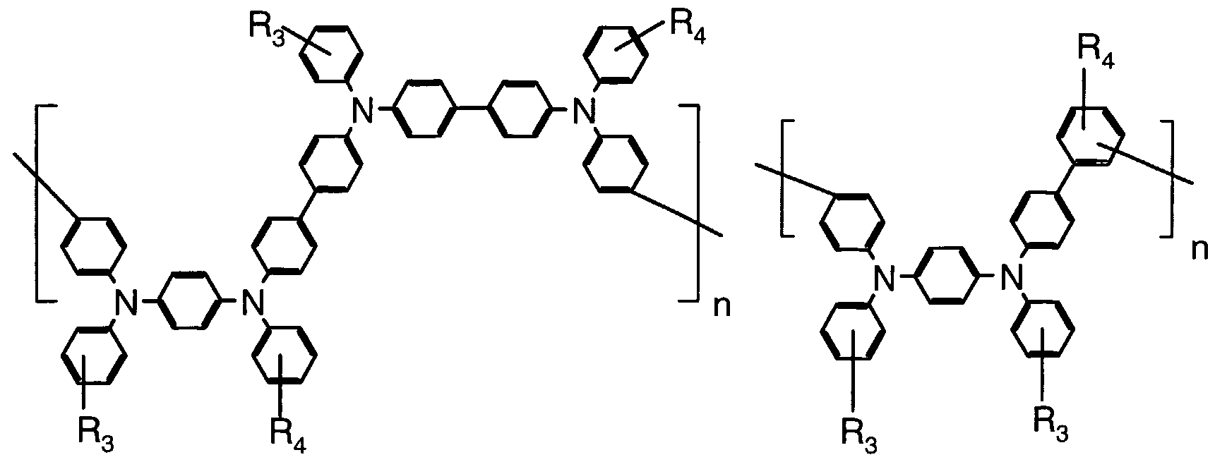
- Polymers with triarylamine moieties in the backbone include, for example, the polymers of Formulas 18, 19, 20, and 21:
- R 3 and R are independently H, alkyl, aryl, alkoxy, aryloxy, arylthio, alkylthio, halo, or -NR a R b , where R a and R b are aryl or alkyl, Ar 9 is aryl or arylene, CM is one or more comonomers, n is an integer of three or greater and preferably 10 or greater, and m is an integer of zero or greater. Each aryl or alkyl portion of any of these substituents can be substituted or unsubstituted.
- Suitable comonomers, CM include, for example, another triarylamine-containing monomer such as those illustrated in Formulas 18-21 or 33-34 below, arylene (including substituted or unsubstituted para- or met ⁇ -phenylene), substituted or unsubstituted styrene comonomers, derivatized carbazole comonomers (such as N-alkyl carbazole or N-aryl carbazole, for example, the comomoners as illustrated in Formulas 29 and 32), ether- and polyether-linked comonomers, carbonate comonomers, urethane-linked comonomers, thioether-linked comonomers, ester-linked comonomers, and imide- and amide-linked comonomers.
- carbazole comonomers such as N-alkyl carbazole or N-aryl carbazole, for example, the comomoners as illustrated in Formulas 29 and 32
- Such comonomers include, but are not limited to, -O-(C n H 2n O)- and -Ar ⁇ o-O-(C n H 2n O)-Ar ⁇ - where Ario and Arn are arylene.
- the comonomer contains one or more photo- or thermocrosslinking functional groups, such a benzocyclobutene (Formula 22) or acrylate or methacrylate groups, such as, for example, the acrylate group of Formula 23.
- photo- or thermocrosslinking functional groups such as a benzocyclobutene (Formula 22) or acrylate or methacrylate groups, such as, for example, the acrylate group of Formula 23.
- cross-linkable moieties are described in, for example, PCT Patent Application Publication No. WO 97/33193, incorporated herein by reference.
- the polymers containing such cross-linkable moieties are selected to crosslink under relatively mild photochemical or thermal conditions.
- thermal crosslinking may occur at 100 to 150 °C
- UV- visible radiation in the range of 300 to 700 nm might be used to crosslink the polymers.
- the comonomer is copolymerized with the triarylamine-containing monomer unit.
- the comonomer can be coupled to the triarylamine-containing monomer unit prior to polymerization.
- Such a polymer might not be considered a copolymer, but rather a homopolymer with the coupled triarylamine- containing unit/comonomer unit as the basic monomer unit of the polymer. Examples of such polymers are illustrated by Formulas 24-27.
- polymers of Formulas 24-27 include the polymers of Formulas 28-32:
- the comonomer unit is coupled to the triarylamine moiety-containing monomer unit in such a way that the two monomer units alternate in the polymer.
- Formulas 33 and 34 illustrate polymers with triarylamine pendent groups:
- R 3 , R 4 , and R 5 are independently H, alkyl, aryl, alkoxy, aryloxy, arylthio, alkylthio, halo, or -NR a R b , where R a and R b are aryl or alkyl, CM is one or more comonomers, n is an integer of three or greater and preferably 10 or greater, and m is an integer of zero or greater. Each aryl or alkyl portion of any of these substituents can be substituted or unsubstituted.
- Suitable comonomers include, for example, another triarylamine- containing monomer containing one or more chain polymerizable moieties, arylenes (including substituted or unsubstituted para- or met ⁇ -phenylene) with one or more chain polymerizable moieties, derivatized carbazole comonomers (such as N-vinyl carbazole), carbonate comonomers, urethane-linked comonomers, thioether-linked comonomers, ester-linked comonomers, imide- and amide-linked comonomers, substituted or unsubstituted styrene comonomers, (meth)acrylate comonomers of, for example, C1-C12 alcohols, diene comonomers such as, for example, butadiene, isoprene and 1,3 cyclohexadiene, and other chain-polymerizable comonomers.
- the comonomer is copolymerized with the triarylamine-containing monomer unit.
- the comonomer can be coupled to the triarylamine-containing monomer unit prior to polymerization.
- Such a polymer might not be considered a copolymer, but rather a homopolymer with the coupled triarylamine- containing unit/comonomer unit as the basic monomer unit of the polymer.
- One example is illustrated as Formula 35.
- the pendent groups can also extend from backbone moieties other than the ethylene moieties illustrated in Formulas 33 and 34.
- backbone units from which the triarylamine pendent groups can extend include, for example, alkylene (such as propylene, butylenes, isoprene, or 1,3-cyclohexadiene), silane, arylenes (including substituted or unsubstituted para- or raet ⁇ -phenylene), derivatized carbazole monomers (as illustrated in Formulas 29 and 32), carbonate monomers, urethane-linked monomers, thioethers-linked monomers, ester-linked monomers, imide- and amide-linked monomers, substituted and unsubstituted styrene monomers, and (meth)acrylate monomers.
- alkylene such as propylene, butylenes, isoprene, or 1,3-cyclohexadiene
- silane such as propylene, butylene
- alkylene group e.g., methylene or ethylene
- arylene an alkyl ether (e.g., -CH 2 -O-) group, or
- each R 3 , R 4 , R 5 , R 6 , and R 7 is independently H, alkyl, aryl, alkoxy, aryloxy, arylthio, alkylthio, halo, or -NR a R b , where R a and R b are aryl or alkyl.
- R a and R b are aryl or alkyl.
- R 3 , R 6 , and R 7 can be H and R 4 can be methyl in any of Formulas 36-38.
- alkyl includes both straight-chained, branched, and cyclic alkyl groups and includes both unsubstituted and substituted alkyl groups. Unless otherwise indicated, the alkyl groups are typically C1-C20. Examples of “alkyl” as used herein include, but are not limited to, methyl, ethyl, n-propyl, n-butyl, n- pentyl, isobutyl, and isopropyl, and the like.
- aryl refers to monovalent unsaturated aromatic carbocyclic radicals having one to fifteen rings, such as phenyl or bipheynyl, or multiple fused rings, such as naphthyl or anthryl, or combinations thereof.
- aryl as used herein include, but are not limited to, phenyl, 2-naphthyl, 1 -naphthyl, biphenyl, 2-hydroxyphenyl, 2-aminophenyl, 2-methoxyphenyl and the like.
- arylene refers to divalent unsaturated aromatic carbocyclic radicals having one to fifteen rings, such as phenylene, or multiple fused rings, such as fluorene, naphthylene or anthrylene, or combinations thereof.
- arylene as used herein include, but are not limited to, benzene- 1,2-diyl, benzene- 1 ,3-diyl, benzene- 1 ,4-diyl, naphthalene- 1 ,8-diyl, anthracene- 1 ,4-diyl, fluorene, phenylenevinylene, phenylenedivinylene, and the like.
- alkoxy refers to the functional group -OR where R is a substituted or unsubstituted alkyl group. Unless otherwise indicated, the alkyl group is typically C1-C20. Examples of “alkoxy” as used herein include, but are not limited to, methoxy, ethoxy, n-propoxy, and 1-methylethoxy, and the like. Unless otherwise indicated, the term “aryloxy” refers to the functional group -OAr where Ar is a substituted or unsubstituted aryl group. Examples of “aryloxy” as used herein include, but are not limited to, phenyloxy, naphthyloxy, and the like.
- Suitable substituents for substituted alkyl, aryl, and arylene groups include, but are not limited to, alkyl, alkylene, aryl, arylene, heteroaryl, heteroarylene, alkenyl, alkenylene, -NRR', F, Cl, Br, I, -OR, -SR, cyano, nitro, -COOH, and -COO-alkyl where R and R' are independently hydrogen, alkyl, or aryl.
- halo includes fluoro, chloro, bromo, and iodo.
- polymer includes homopolymers and copolymers including block copolymers and random copolymers.
- the buffer layer also includes an electron acceptor material to improve electron transport.
- an electron acceptor material to improve electron transport.
- such compounds have relatively high electron affinity and relatively low energy of the lowest unoccupied molecular orbital (LUMO).
- Suitable electron acceptor materials include electron deficient compounds such as, for example, tetracyanoquinodimethane and derivatives, thiopyranylidines, polynitrofluorenones, tetracyanoethylene (TCNE), chloranil, and other compounds commonly used as electron acceptors in charge transfer materials and electrophotography.
- electron acceptor materials include tetracyanoquinodimethane (TCNQ) (Formula 39), tetrafluoro-tetracyanoquinodimethane (F 4 -TCNQ) (Formula 40), tetracyanoethylene, chloranil, 2-(4-(l-methylethyl)phenyl-6- phenyl-4H-thiopyran-4-ylidene)-propanedinitrile-l,l-dioxyide (PTYPD) (Formula 41), and 2,4,7-trinitrofluorenone (Formula 42).
- TCNQ tetracyanoquinodimethane
- F 4 -TCNQ tetrafluoro-tetracyanoquinodimethane
- PTYPD 2-(4-(l-methylethyl)phenyl-6- phenyl-4H-thiopyran-4-ylidene)-propanedinitrile-l,l-dioxyide
- the electron acceptor material is soluble in one or more organic solvents, more preferably, one or more organic solvents in which the triarylamine material is also soluble.
- the electron donor material is present in the buffer layer in the range of 0.5 to 20 wt.% of the triarylamine material. In some embodiments, the electron donor material is present in the buffer layer in the range of 1 to 5 wt.% of the triarylamine material.
- the buffer layer optionally includes a polymeric binder.
- the polymeric binder can include inert or electroactive polymers or combinations thereof. Suitable polymers for the polymeric binder include, for example, polystyrene, poly(N-vinyl carbazole), polyfluorenes, poly(para-phenylenes), poly(phenylenevinylenes), polycarbonates, polyimides, polyolefins, polyacrylates, polymethacrylates (for example, poly(methylmethacrylate)), polyethers, polysulfones, polyether ketones, and copolymers or mixtures thereof.
- the triarylamine material includes a triarylamine-containing polymer
- that polymer can act as or in cooperation with a polymeric binder, if desired.
- the polymeric binder is typically provided in the range of 20 to 150 wt.%, preferably 70 to 120 wt.%, of the triarylamine material.
- the polymeric binder can be photochemically or thermally crosslinked with itself or with other components in the buffer layer.
- a thermochemical or photochemical crosslinking agent such as, for example, 2,6-bis(4- azidobenzylidene)-4-methylcyclohexanone, can optionally be included in the buffer layer.
- Crosslinking can be desirable for one or more purposes, such as decreasing the migration of buffer layer components out of the buffer layer, decreasing the migration of other materials into the buffer layer, increasing thermal stability, increasing mechanical stability, increasing morphological stability, increasing buffer layer stability, and increasing layer integrity, particularly during further solution processing.
- Crosslinking the buffer layer can also facilitate manufacture of a device by providing a buffer layer upon which other layers can be solution coated or cast with substantially less concern about dissolving the buffer layer.
- the buffer layer can optionally include a color converting material.
- This material can be a luminescent or non-luminescent organic, organometallic, or inorganic compound or combinations thereof.
- the color converting material changes the color of electroluminescence from an emitting layer by selective absorption of light or by absorption of light and re-emission of the light in a different spectral range.
- Suitable materials include, for example, dyes, pigments, and nanoparticles. Examples of suitable non-luminescent and luminescent dyes include: azo dyes (e.g.
- anthraquinone dyes e.g. C.I. Reactive Blue 4 and others
- indigoid dyes e.g. Tyrian Purple and others
- triphenylmethane-based dyes e.g. Eosin and others
- coumarin dyes e.g. Coumarin 6 and others
- metal porphyrins e.g. platinum [II] octaethylporphyrin and others
- cyclometalated transition metal complexes e.g. iridium tris(2-phenylpyridine) and others
- other dyes including those discussed in H.Zollinger, Color Chemistry.
- the color converting material can be polymeric with color converting moieties in the backbone, on pendant chains, or both.
- the color converting material if used, is typically included in the buffer layer in an amount in the range of 0.1 to 100 wt.%, preferably 0.1 to 10 wt.%, of the triarylamine material.
- the buffer layer can also optionally include scattering material, such as small particles, nanocrystals, or clusters.
- suitable materials include clays, oxides, metals, and glasses.
- Specific examples of suitable materials include titania, alumina and silica powders having a mean particle size of approximately 0.05 to 0.2 microns, and added to the buffer layer composition in a concentration of from 0.1 to 20% by weight, and preferably from about 1-5% by weight.
- the buffer layer 254 is formed by solution coating the material of the buffer layer onto the substrate 250.
- additional layers such as the hole transport layer 260 or emission layer 256, can be formed on the buffer layer by a variety of techniques including, for example, solution coating, physical or chemical vapor deposition, and thermal transfer, including light-induced thermal transfer as described below.
- An organic solvent is used to make the solution for the buffer layer.
- suitable organic solvents include carbon tetrachloride, toluene, chloroform, 1,2- dichloroethane, 1 ,2-dichlorobenzene, tetrahydrofuran, pyridine, and the like.
- the remaining materials of the buffer layer are typically dispersible or, preferably, soluble in the organic solvent.
- layers are formed using solutions of components in water.
- a drawback of these methods is that some of the device materials are degraded in the presence of water or irreversible physical changes may occur leading to device degradation. Thus, if a layer is formed using a water solution, the water generally must be completely removed.
- organic solvents can be chosen that are easier to remove or do not degrade materials in the device or both.
- the materials of a layer are disposed by vapor deposition.
- a number of materials are difficult to accurately and consistently deposit by vapor deposition methods. Included in these materials are a variety of polymers and ionic compounds. Thus, it can be difficult to deposit materials such as a polymeric binder and cross-linking agent using vapor deposition techniques. In addition, the consistency and uniformity of a vapor deposited composition becomes increasingly difficult when the composition contains multiple components.
- forming a buffer layer by solution coating can facilitate the use of materials such as polymeric binders, polymeric triarylamine materials, cross-linking agents, dyes, pigments, scattering particles, and so on.
- the coating technique permits the use of multi-component systems when all of the components are soluble or dispersible in the solvent.
- the buffer layer material can be coated onto a donor sheet and then transferred by techniques such as thermal transfer to the substrate. This can be particularly useful for patterning the buffer layer onto the substrate.
- the buffer layer material can be selectively transferred from the donor sheet to the substrate according to a pattern by selective application of, for example, light or heat to the donor sheet. This can be useful, for example, to pattern individual buffer layers with a different color converting materials (or lack of color converting material) onto the substrate.
- a full-color display could be formed using, for example, three different buffer layers with three different color converting materials (or two different color converting materials and the third buffer layer lacking a color converting material).
- Other methods of selectively patterning color converting materials in buffer layer(s) include, for example, thermal diffusion of the color converting material, inkjet transfer of the buffer material with (or without) color converting materials onto the substrate, and selective photobleaching.
- Suitable thermal transfer methods for transferring a buffer layer or other device layers to the substrate or onto a previously-formed buffer layer include, for example, thermal head transfer methods and light-induced thermal transfer methods.
- the presence of the buffer layer on the substrate can, at least in some instances, facilitate the transfer of other layers to the substrate by these methods.
- Materials, layers, or other structures can be selectively transferred from the transfer layer of a donor sheet to a receptor substrate by placing the transfer layer of the donor element adjacent to the receptor and selectively heating the donor element.
- the donor element can be selectively heated by irradiating the donor element with imaging radiation that can be absorbed by light-to-heat converter material disposed in the donor, often in a separate light-to-heat conversion
- the donor can be exposed to imaging radiation through the donor substrate, through the receptor, or both.
- the radiation can include one or more wavelengths, including visible light, infrared radiation, or ultraviolet radiation, for example from a laser, lamp, or other radiation source.
- thermal print heads or other heating elements may be particularly suited for making lower resolution patterns of material or for patterning elements whose placement need not be precisely controlled.
- Material from the transfer layer can be selectively transferred to a receptor in this manner to imagewise form patterns of the transferred material on the receptor.
- thermal transfer using light from, for example, a lamp or laser, to patternwise expose the donor can be advantageous because of the accuracy and precision that can often be achieved.
- the size and shape of the transferred pattern (e.g., a line, circle, square, or other shape) can be controlled by, for example, selecting the size of the light beam, the exposure pattern of the light beam, the duration of directed beam contact with the donor sheet, or the materials of the donor sheet.
- the transferred pattern can also be controlled by irradiating the donor element through a mask.
- Transfer layers can also be transferred from donor sheets without selectively transferring the transfer layer.
- a transfer layer can be formed on a donor substrate that, in essence, acts as a temporary liner that can be released after the transfer layer is contacted to a receptor substrate, typically with the application of heat or pressure.
- lamination transfer Such a method, referred to as lamination transfer, can be used to transfer the entire transfer layer, or a large portion thereof, to the receptor.
- a donor sheet for light-induced thermal transfer can include, for example, a donor substrate, an optional underlayer, an optional light-to-heat conversion (LTHC) layer, an optional interlayer, and a transfer layer.
- the donor substrate can be a polymer film or any other suitable, preferably transparent, substrate.
- the donor substrate is also typically selected from materials that remain stable despite heating of one or more layers of the donor.
- the inclusion of an underlayer between the substrate and an LTHC layer can be used to insulate the substrate from heat generated in the LTHC layer during imaging.
- the underlayer can include materials that impart desired mechanical or thermal properties to the donor element.
- the underlayer can include materials that exhibit a low value for the mathematical product of specific heat and density or low thermal conductivity relative to the donor substrate. Such an underlayer may be used to increase heat flow to the transfer layer, for example to improve the imaging sensitivity of the donor.
- the underlayer can also include materials for their mechanical properties or for adhesion between the substrate and the LTHC.
- An LTHC layer can be included in donor sheets of the present invention to couple irradiation energy into the donor sheet.
- the LTHC layer preferably includes a radiation absorber that absorbs incident radiation (e.g., laser light) and converts at least a portion of the incident radiation into heat to enable transfer of the transfer layer from the donor sheet to the receptor.
- An optional interlayer can be disposed between the LTHC layer and transfer layer.
- the interlayer can be used, for example, to minimize damage and contamination of the transferred portion of the transfer layer and may also reduce distortion in the transferred portion of the transfer layer.
- the interlayer can also influence the adhesion of the transfer layer to the rest of the donor sheet.
- the interlayer has high thermal resistance.
- the interlayer does not distort or chemically decompose under the imaging conditions, particularly to an extent that renders the transferred image non-functional.
- the interlayer typically remains in contact with the LTHC layer during the transfer process and is not substantially transferred with the transfer layer.
- the interlayer can provide a number of benefits, if desired.
- the interlayer can be a barrier against the transfer of material from the light-to-heat conversion layer. It can also modulate the temperature attained in the transfer layer so that thermally unstable materials can be transferred.
- the interlayer can act as a thermal diffuser to control the temperature at the interface between the interlayer and the transfer layer relative to the temperature attained in the LTHC layer. This can improve the quality (i.e., surface roughness, edge roughness, etc.) of the transferred layer.
- the presence of an interlayer can also result in improved plastic memory in the transferred material.
- the thermal transfer layer includes the buffer material to form the buffer layer, if desired, or appropriate materials to form other layers depending on the desired thermal transfer.
- other layers of the device such as the hole transport layer or the emission layer, can be transferred onto the substrate or onto the buffer layer or other layers disposed on the substrate by these methods.
- Such transfer can be sequential using multiple donor sheets or, in some embodiments, multiple layers can be transferred using a single donor sheet with the transfer layer having individual sublayers.
- the present invention contemplates light emitting OEL displays and devices.
- OEL displays can be made that emit light and that have adjacent devices that can emit light having different color.
- Figure 5 shows an OEL display 300 that includes a plurality of OEL devices 310 disposed on a substrate 320. Adjacent devices 310 can be made to emit different colors of light. The separation shown between devices 310 is for illustrative purposes only.
- Adjacent devices may be separated, in contact, overlapping, etc., or different combinations of these in more than one direction on the display substrate.
- a pattern of parallel striped transparent conductive anodes can be formed on the substrate followed by a striped pattern of a hole transport material and a striped repeating pattern of red, green, and blue light emitting LEP layers, followed by a striped pattern of cathodes, the cathode stripes oriented perpendicular to the anode stripes.
- Such a construction may be suitable for forming passive matrix displays.
- transparent conductive anode pads can be provided in a two-dimensional pattern on the substrate and associated with addressing electronics such as one or more transistors, capacitors, etc., such as are suitable for making active matrix displays.
- display 300 can be a multiple color display. As such, it may be desirable to position optional polarizer 330 between the light emitting devices and a viewer, for example to enhance the contrast of the display.
- each of the devices 310 emits light.
- OEL backlights can include emissive layers. Constructions can include bare or circuitized substrates, anodes, cathodes, hole transport layers, electron transport layers, hole injection layers, electron injection layers, emissive layers, color changing layers, and other layers and materials suitable in OEL devices. Constructions can also include polarizers, diffusers, light guides, lenses, light control films, brightness enhancement films, and the like. Applications include white or single color large area single pixel lamps, for example where an emissive material is provided by thermal stamp transfer, lamination transfer, resistive head thermal printing, or the like; white or single color large area single electrode pair lamps that have a large number of closely spaced emissive layers patterned by laser induced thermal transfer; and tunable color multiple electrode large area lamps.
- Low resolution OEL displays can include emissive layers. Constructions can include bare or circuitized substrates, anodes, cathodes, hole transport layers, electron transport layers, hole injection layers, electron injection layers, emissive layers, color changing layers, and other layers and materials suitable in OEL devices. Constructions can also include polarizers, diffusers, light guides, lenses, light control films, brightness enhancement films, and the like.
- Applications include graphic indicator lamps (e.g., icons); segmented alphanumeric displays (e.g., appliance time indicators); small monochrome passive or active matrix displays; small monochrome passive or active matrix displays plus graphic indicator lamps as part of an integrated display (e.g., cell phone displays); large area pixel display tiles (e.g., a plurality of modules, or tiles, each having a relatively small number of pixels), such as may be suitable for outdoor display used; and security display applications.
- graphic indicator lamps e.g., icons
- segmented alphanumeric displays e.g., appliance time indicators
- small monochrome passive or active matrix displays e.g., small monochrome passive or active matrix displays plus graphic indicator lamps as part of an integrated display (e.g., cell phone displays); large area pixel display tiles (e.g., a plurality of modules, or tiles, each having a relatively small number of pixels), such as may be suitable for outdoor display used; and security display applications.
- High resolution OEL displays can include emissive layers. Constructions can include bare or circuitized substrates, anodes, cathodes, hole transport layers, electron transport layers, hole injection layers, electron injection layers, emissive layers, color changing layers, and other layers and materials suitable in OEL devices. Constructions can also include polarizers, diffusers, light guides, lenses, light control films, brightness enhancement films, and the like. Applications include active or passive matrix multicolor or full color displays; active or passive matrix multicolor or full color displays plus segmented or graphic indicator lamps (e.g., laser induced transfer of high resolution devices plus thermal hot stamp of icons on the same substrate); and security display applications.
- ITO substrates were prepared as follows: ITO (indium tin oxide) glass substrates (Applied Films Corporation, CO; ca. 25 ⁇ /sq.) were rinsed in acetone (Aldrich Chemical Company), dried with nitrogen, and rubbed with TX1010
- This Example describes the formation of OLEDs having a solution-processed hole- injecting buffer layer incorporating 4,4',4"-tris(N-3-methylphenyl-N- phenylamino)triphenylamine (MTDATA) as a triarylamine material, polystyrene (PS) as an electrically inert polymer binder, and tetrafluoro-tetracyanoquinodimethane (F 4 -TCNQ) or tetracyanoquinodimethane (TCNQ) as an electron accepting dopant material.
- MTDATA 4,4',4"-tris(N-3-methylphenyl-N- phenylamino)triphenylamine
- PS polystyrene
- F 4 -TCNQ tetrafluoro-tetracyanoquinodimethane
- TCNQ tetracyanoquinodimethane
- the OLED is prepared by vapor depositing, onto an ITO substrate with a buffer layer, 20 nm of N,N'-bis(naphthan-2-yl)-N,N'-bis(phenyl)benzidine (NPD, H.W. Sands Corp., Jupiter, FL), followed by 30 nm of aluminum tris(8-hydroxyquinolate) (AIQ, H.W. Sands Corp, Jupiter, FL.) doped with ca. 1 wt.% of green-emitting Coumarin 545T (C545T, Eastman Kodak Co., Rochester, NY), and followed by 20 nm of AIQ.
- the OLED was capped with a cathode composed of ca.
- the NPD layer acts as a hole-transport layer and electron-blocking layer
- the layer of AIQ doped with C545T acts as a light emitting layer
- the layer of AIQ acts as an electron injection and transport layer.
- All organic and cathode layers except the buffer layers were fabricated in a standard vacuum-deposition procedure at a base vacuum of ca. 10 "7 tolO "5 torr (about 10 *5 to 10 "3 Pa) with evaporation rates of 0.05-0.2 nm/s for organic materials, 0.05 nm/s for LiF, and 1.5-2 nm s for Al.
- Comparative Example 1 polypyrrole (PPY, Aldrich Chemical Co.) was used as a control hole-injecting buffer layer for purposes of comparison of the OLED behavior of the devices deposited onto PPY and onto doped triarylamine-based buffer layers.
- PPY was spun-coat from its water suspension after filtering the suspension through 0.2 ⁇ m Nylon microfilters, followed by annealing under nitrogen gas flow at 110°C for ca. 15 min.
- OLEDs with buffer layers containing MTDATA, PS, and TCNQ were prepared and their performance evaluated along with that of the control PPY-based OLEDs.
- MTDATA, PS, and TCNQ were purchased from HWSands Corp. (Jupiter, FL),
- the buffer layers were spun-coat from their ca. 1.5 wt.% solutions in toluene at the spin- rate of 2000 RPM (about 33 s "1 ) to form ca. 90 nm thick films on the ITO coated substrates.
- the device structures are glass-ITO/buffer layer/NPD/AlQ:C545T/AlQ/LiF/Al.
- the buffers layers for the Examples are:
- Example. 1 31 wt. % PS, 62 wt.% MTDATA, and 7 wt.% TCNQ
- Example 2 47 wt. % PS, 46 wt.% MTDATA, and 7 wt.% TCNQ
- Example 3 62 wt. % PS, 31 wt.% MTDATA, and 7 wt.% TCNQ
- No short-circuiting was observed in any of the studied electroluminescent lamps.
- the OLEDs showed high operational efficiency and low operational voltages, with operational voltages decreasing with increasing triarylamine concentration.
- High bandgap hole-transporting ⁇ oly(N-vinylcarbazole) (PVK, Polymer Source Inc., Dorval, Quebec) having relatively high oxidation potential (ca. IV vs. SCE) and low hole mobility (ca. 10 "6 - 10 s cm 2 /V*s (about 10 "10 - 10 "9 m 2 /V s)) was used as an electroactive binder in the following buffer compositions: a) 60 wt. % PVK and 40 wt.%
- Example 5 60 wt.% PVK and 40 wt.% MTDATA
- Example 6 56 wt.% PVK, 37 wt.% MTDATA, and 7 wt.% F 4 -TCNQ.
- Luminance-voltage-current density screening of the OLEDs indicated that high efficiencies can be obtained in the composition including triarylamine-based buffers along with low operational voltages. Doping the PVK:MTDATA blend with F 4 -TCNQ significantly lowered the operational voltage of the OLEDs. Operational lifetime studies on the triarylamine-based compositions, in which the OLEDs were driven at a constant current of ca. 1.8 mA/cm (about 18 A/m ) under inert atmosphere, show that projected operation lifetimes of these OLEDs extend into 10 3 -10 4 hours range at an initial luminance of several hundred Cd/m 2 . Examples 7 and 8 Buffer Layers containg Copolymers withTriarylamine Moieties Pendant to a
- doped triarylamine buffer layers based on copolymers incorporating triarylamine moieties as a functionality pendant to a polyolefin backbone were incorporated into OLEDs.
- a block co-polymer of styrene with diphenylaminostyrene (PS-pDPAS), having approximately 6: 1 molar ratio of the monomers was synthesized and screened as a triarylamine-containing polymer. All materials are available from Aldrich Chemical Co., Milwaukee, WI, with the exception of p-diphenylaminostyrene, and as where noted. This monomer was synthesized by a preparation similar to that described by G. N. Tew, M. U. Pralle, and S. I. Stupp in Angew. Chem. Int. Ed., 2000, 39, 517, incorporated herein by reference.
- the crude solid was purified by column chromatography on silica gel using a 50/50 mixture of methylene chloride and hexane to give a yellow solid that was further recrystallized once from hexane (15.37 g, 78%).
- a round-bottom glass reactor was baked out under vacuum at 200 °C for 2 hours, then allowed to cool.
- the reactor was filled with dry nitrogen. Subsequently, 71.8 g of cyclohexane and 4.4 mL of tetrahydrofuran (THF) were added to the reactor by syringe.
- THF tetrahydrofuran
- the THF was distilled from sodium/benzophenone solution under nitrogen prior to use, in order to scavenge water and oxygen.
- the cyclohexane was dried by passage through activated basic alumina, followed by sparging with nitrogen gas for 30 minutes prior to use. After addition of the solvents, the reaction flask was cooled to 3 °C in an ice water bath, after which 0.02 mL of styrene was added to the reactor. The styrene had previously been passed through activated basic alumina to remove inhibitors and water, and sparged with nitrogen gas to remove oxygen.
- a solution of s-butyllithium in cyclohexane (0.4 mL, 1.3 mol/L) was subsequently added to the reactor.
- the molecular weight of the block copolymer was 7700 g/mol, based on gel permeation chromatography in THF against polystyrene standards.
- OLED preparation OLEDs were formed as described in the Comparative Example 1 and Examples 1-
- Example 7 PS-pDPAS
- Example 8 93 wt.% PS-pDPAS and 7 wt.% F 4 -TCNQ.
- buffer layers were spun-coat from their ca. 1.5% wt. solutions in toluene at the spin-rate of 2000 RPM (about 33 s "1 ) to form ca. 90 nm thick films on the ITO coated substrates.
- the buffer layers include PEDT
- Cz-triarylamine as a triarylamine-containing co- polymer for hole injecting buffer layers lies in the presence of phenylenediamine linkages, which typically cause lower ionization potential (higher energy of the highest occupied molecular orbital). This provides favorable conditions for increased conductivity due to doping with electron acceptors (e.g. F -TCNQ).
- electron acceptors e.g. F -TCNQ
- the reaction was stirred for 20 minutes and then warmed to -50°C
- the temperature was reduced to -78°C and 2-isopropoxy-4,4,5,5-tetramethyl-l,3,2-dioxaborolane (64 g, 0.34 mole) added via syringe at such a rate as to maintain the temperature below -60 °C
- the reaction was maintained at -78 °C for two hours and then poured into an aqueous solution of ammonium acetate (90 g in 2100 mL water). The layers were phase separated and the aqueous phase extracted with methyl tert-butyl ether (2 x 200 mL).
- tetrakistriphenylphosphine palladium (0) (10 mg, 0.0.0068 mmole, 0.02 equivalents) was added. The reaction mixture was then refluxed for 16 hrs. A solution of 0.5g bromobenzene in 5 mL purged toluene was added followed by and a further charge of tetrakistriphenylphosphine paladium (0) (10 mg) and refluxing then continued for a further 16 hrs.
- OLEDs were formed as described in the Comparative Example 1 and Examples 1- 3 except that the buffer layers were as follows:
- Example 10 93 wt.% Cz-triarylamine and 7 wt.% F -TCNQ. These buffer layers were spun-coat from their ca. 1.5% wt. solutions in toluene at the spin- rate of 2000 RPM (about 33 s "1 ) to form ca. 90 nm thick films on the ITO coated substrates.
- This Example describes the fabrication of hole-injecting solution-processed buffer layers based on doped triarylamines blended with electroactive polymer binder and blended with color-converting organic dye material in order to tune electroluminescence energy and CIE color coordinates of the OLEDs incorporating such buffer layers.
- PVK poly( vinyl carbazole)
- MTDATA H.W. Sands Corp., Jupiter, FL
- F 4 -TCNQ
- the Dye can be prepared according to U.S. Patent No. 5,639,896, incorporated herein by reference and is available as "Amaplast Blue RFC" supplied by "American Aniline Products", N.Y., N.Y., a unit of Koppers Co., Pittsburgh, PA. Each solution was then spun coat onto cleaned ITO substrates at 3000 R.P.M. for 30s.
- a vapor deposited small-molecule OLED with NPD (20 nm, 0.2 nm/s), AIQ (50 nm, 0.1 nm s), LiF (0.7 nm, 0.05 nm/s), Al (200 nm, 2 nm/s) was sequentially deposited on top in a standard vacuum deposition procedure at 10 "6 torr (about 10 "4 Pa) as described in Comparative Example 1 and Examples 1-3.
- OLEDs were formed as described in the Comparative Example 1 and Examples 1-
- Example 11 Solution a) corresponding to 58 wt.% PVK, 38 wt.% MTDATA, and
- Example 12 Solution b) corresponding to 24 wt.% PVK, 16 wt.% MTDATA, 2 wt.% F 4 -TCNQ, and 58 wt.% Dye
- Example 13 Solution c) corresponding to 18 wt.% PVK, 12 wt.% MTDATA, 1 wt.% F 4 -TCNQ, and 69 wt.% Dye.
- a thermal transfer donor sheet was prepared in the following manner: An LTHC solution, given in Table ⁇ , was coated onto a 0.1 mm thick polyethylene terephthalate (PET) film substrate (M7 from Teijin, Osaka, Japan). Coating was performed using a Yasui Seiki Lab Coater, Model CAG-150, using a microgravure roll with 150 helical cells per inch. The LTHC coating was in-line dried at 80°C and cured under ultraviolet (UV) radiation.
- PET polyethylene terephthalate
- MTDATA (4,4' ,4"-tris(N-(3-methylphenyl)-N- ⁇ henylamino)triphenylamine) (OS A 3939, H. W. Sands Corp., Jupiter, FL) 1.0 % (w/w) in toluene was filtered and dispensed through a Whatman Puradisc TM 0.45 ⁇ m Polypropylene (PP) syringe filter.
- PVK Poly(9-vinylcarbazole) (Aldrich Chemical Co., Milwaukee, WI) 1.0 % (w/w) in ttoolluueennee wwaass fifilltteerreedd aanndd ddiissppeennsseedd through a Whatman Puradisc TM 0.45 ⁇ m Polypropylene (PP) syringe filter.
- F j -TCNQ Tetrafluorotetracyanoquinodimethane (Tokyo Kasei Kogyo Co., Tokyo, Japan)
- MTDATA/F4-TCNO 98/2 w/w% mixture of MTDATA/F 4 -TCNQ.
- MTDATA/PVK 65/35 w/w% mixture of MTDATA/PVK
- Receptors were formed as follows: lTO(indium tin oxide) glass (Delta).
- Covion Super Yellow Covion PPV polymer PDY 132 "Super Yellow” (75 mg) from Covion Organic Semiconductors GmbH, Frankfurt, Germany was weighed out into an amber vial with a PTFE cap. To this was added 9.925g of toluene (HPLC grade obtained from Aldrich Chemical, Milwaukee, WI). The solution was stirred over night. The solution was filtered through a 5 ⁇ m Millipore Millex syringe filter.
- PP polypropylene
- Transfer layers were formed on the donor sheets using a 33/67 w/w% blend of the solutions of Covion Super Yellow and polystyrene from the previous section. To obtain the blends, the above-described solutions were mixed at the appropriate ratios and the resulting blend solutions were stirred for 20 min at room temperature.
- the transfer layers were disposed on the donor sheets by spinning (Headway Research spincoater) the blend solution at about 2000-2500 rpm for 30 s to yield a film thickness of approximately 100 nm.
- the donor sheets coated with Covion Super Yellow/polystyrene were brought into contact with each of the receptor substrates prepared in an above section.
- the donor sheets were imaged using two single-mode Nd:YAG lasers. Scanning was performed using a system of linear galvanometers, with the combined laser beams focused onto the image plane using an f-theta scan lens as part of a near-telecentric configuration.
- the laser energy density was 0.4 to 0.8 J/cm .
- the laser spot size, measured at the 1/e intensity was 30 micrometers by 350 micrometers.
- the linear laser spot velocity was adjustable between 10 and 30 meters per second, measured at the image plane.
- the laser spot was dithered perpendicular to the major displacement direction with about a 100 nm amplitude.
- the transfer layers were transferred as lines onto the receptor substrates, and the intended width of the lines was about 100 nm.
- Electroluminescent devices were prepared by depositing calcium/silver cathodes on top of the LEP (Covion Super Yellow/PS) transferred in the above section. Approximately 40 nm of calcium was vapor deposited at a rate of 0.11 nm/s onto the LEP, followed by approximately 400 nm of silver at a rate of 0.5 nm s. In all cases, diode behavior and yellow light emission was observed.
Abstract
Description


Claims
Priority Applications (6)
| Application Number | Priority Date | Filing Date | Title |
|---|---|---|---|
| DE60312861T DE60312861T2 (en) | 2002-06-26 | 2003-05-07 | BUFFER LAYERS FOR ORGANIC ELECTROLUMINESCENZING DEVICES AND METHOD FOR THE PRODUCTION THEREOF AND THEIR USE |
| EP03777517A EP1518281B8 (en) | 2002-06-26 | 2003-05-07 | Buffer layers for organic electroluminescent devices and methods of manufacture and use |
| KR1020047021123A KR101011428B1 (en) | 2002-06-26 | 2003-05-07 | Buffer layers for organic electroluminescent devices and methods of manufacture and use |
| MXPA04012432A MXPA04012432A (en) | 2002-06-26 | 2003-05-07 | Buffer layers for organic electroluminescent devices and methods of manufacture and use. |
| JP2004532564A JP2005531915A (en) | 2002-06-26 | 2003-05-07 | Buffer layer for organic electroluminescent devices, and methods of manufacture and use |
| AU2003286999A AU2003286999A1 (en) | 2002-06-26 | 2003-05-07 | Buffer layers for organic electroluminescent devices and methods of manufacture and use |
Applications Claiming Priority (2)
| Application Number | Priority Date | Filing Date | Title |
|---|---|---|---|
| US10/183,717 US20040004433A1 (en) | 2002-06-26 | 2002-06-26 | Buffer layers for organic electroluminescent devices and methods of manufacture and use |
| US10/183,717 | 2002-06-26 |
Publications (2)
| Publication Number | Publication Date |
|---|---|
| WO2004021463A2 true WO2004021463A2 (en) | 2004-03-11 |
| WO2004021463A3 WO2004021463A3 (en) | 2004-07-29 |
Family
ID=29999217
Family Applications (1)
| Application Number | Title | Priority Date | Filing Date |
|---|---|---|---|
| PCT/US2003/014466 WO2004021463A2 (en) | 2002-06-26 | 2003-05-07 | Buffer layers for organic electroluminescent devices and methods of manufacture and use |
Country Status (12)
| Country | Link |
|---|---|
| US (4) | US20040004433A1 (en) |
| EP (1) | EP1518281B8 (en) |
| JP (1) | JP2005531915A (en) |
| KR (1) | KR101011428B1 (en) |
| CN (2) | CN101325247A (en) |
| AT (1) | ATE358336T1 (en) |
| AU (1) | AU2003286999A1 (en) |
| DE (1) | DE60312861T2 (en) |
| MX (1) | MXPA04012432A (en) |
| MY (1) | MY135888A (en) |
| TW (1) | TW200402248A (en) |
| WO (1) | WO2004021463A2 (en) |
Cited By (13)
| Publication number | Priority date | Publication date | Assignee | Title |
|---|---|---|---|---|
| EP1531501A3 (en) * | 2003-11-13 | 2005-09-07 | International Manufacturing and Engineering Services Co., Ltd. | Organic electroluminescent devices |
| WO2006040704A1 (en) * | 2004-10-12 | 2006-04-20 | Philips Intellectual Property & Standards Gmbh | Electroluminescent light source |
| WO2006061954A1 (en) * | 2004-12-08 | 2006-06-15 | Fuji Electric Holdings Co., Ltd. | Organic el element |
| JP2006190995A (en) * | 2004-12-06 | 2006-07-20 | Semiconductor Energy Lab Co Ltd | Composite material comprising organic compound and inorganic compound, light emitting element and light emitting device employing the composite material as well as manufacturing method of the light emitting element |
| JP2006216858A (en) * | 2005-02-04 | 2006-08-17 | Institute Of Physical & Chemical Research | Organic el element |
| JP2006332047A (en) * | 2005-05-20 | 2006-12-07 | Lg Phillips Lcd Co Ltd | Display element having metal organic mixed layer anode |
| US7977865B2 (en) | 2005-03-23 | 2011-07-12 | Semiconductor Energy Laboratory Co., Ltd. | Composite material, material for light-emitting element, light-emitting element, light-emitting device and electronic device |
| JP2012039131A (en) * | 2004-12-06 | 2012-02-23 | Semiconductor Energy Lab Co Ltd | Light-emitting element and its manufacturing method |
| US8178870B2 (en) | 2008-04-23 | 2012-05-15 | Panasonic Corporation | Organic electroluminescence element |
| US8440325B2 (en) | 2005-12-22 | 2013-05-14 | Cambridge Display Technology Limited | Electronic device |
| US9590179B2 (en) | 2011-03-28 | 2017-03-07 | Nippon Steel & Sumikin Chemical Co., Ltd. | Curable composition, cured product, and organic electroluminescent element using same |
| WO2017217727A1 (en) * | 2016-06-15 | 2017-12-21 | 코오롱인더스트리 주식회사 | Organic solar cell and method for manufacturing same |
| KR101825871B1 (en) | 2014-06-20 | 2018-02-05 | 코니카 미놀타 가부시키가이샤 | Electroluminescent element design method and electroluminescent element manufacturing method using such design method |
Families Citing this family (155)
| Publication number | Priority date | Publication date | Assignee | Title |
|---|---|---|---|---|
| KR100652039B1 (en) * | 2000-11-23 | 2006-11-30 | 엘지.필립스 엘시디 주식회사 | Electroluminescence Device |
| US20040004433A1 (en) * | 2002-06-26 | 2004-01-08 | 3M Innovative Properties Company | Buffer layers for organic electroluminescent devices and methods of manufacture and use |
| JP2004063363A (en) * | 2002-07-31 | 2004-02-26 | Semiconductor Energy Lab Co Ltd | Material for electroluminescent element and electroluminescent element using the material |
| TWI280973B (en) * | 2002-08-28 | 2007-05-11 | Sumitomo Chemical Co | Polymer compound and polymer light-emitting device using the same |
| WO2004029133A1 (en) * | 2002-09-24 | 2004-04-08 | E.I. Du Pont De Nemours And Company | Water dispersible polyanilines made with polymeric acid colloids for electronics applications |
| US7317047B2 (en) * | 2002-09-24 | 2008-01-08 | E.I. Du Pont De Nemours And Company | Electrically conducting organic polymer/nanoparticle composites and methods for use thereof |
| CN100540628C (en) * | 2002-09-24 | 2009-09-16 | E.I.内穆尔杜邦公司 | Conductive organic polymer/nanoparticle composition and application method thereof |
| CA2499377A1 (en) * | 2002-09-24 | 2004-04-08 | E. I. Du Pont De Nemours And Company | Water dispersible polythiophenes made with polymeric acid colloids |
| KR100518419B1 (en) * | 2002-11-06 | 2005-09-29 | 엘지.필립스 엘시디 주식회사 | Organic Electro luminescence Device |
| CN1826840B (en) * | 2002-12-19 | 2010-06-23 | 株式会社半导体能源研究所 | Light emitting device and a method of manufacturing thereof |
| US7338820B2 (en) * | 2002-12-19 | 2008-03-04 | 3M Innovative Properties Company | Laser patterning of encapsulated organic light emitting diodes |
| US6869699B2 (en) * | 2003-03-18 | 2005-03-22 | Eastman Kodak Company | P-type materials and mixtures for electronic devices |
| US7390438B2 (en) * | 2003-04-22 | 2008-06-24 | E.I. Du Pont De Nemours And Company | Water dispersible substituted polydioxythiophenes made with fluorinated polymeric sulfonic acid colloids |
| US20060099448A1 (en) * | 2003-04-28 | 2006-05-11 | Zheng-Hong Lu | Top light-emitting devices with fullerene layer |
| US7259443B2 (en) * | 2003-06-26 | 2007-08-21 | E.I. Du Pont De Nemours And Company | Methods for forming patterns on a filled dielectric material on substrates |
| KR100657891B1 (en) * | 2003-07-19 | 2006-12-14 | 삼성전자주식회사 | Semiconductor nanocrystal and method for preparing the same |
| JP4378186B2 (en) * | 2004-02-06 | 2009-12-02 | キヤノン株式会社 | Organic EL element array |
| US7365230B2 (en) * | 2004-02-20 | 2008-04-29 | E.I. Du Pont De Nemours And Company | Cross-linkable polymers and electronic devices made with such polymers |
| US7351358B2 (en) | 2004-03-17 | 2008-04-01 | E.I. Du Pont De Nemours And Company | Water dispersible polypyrroles made with polymeric acid colloids for electronics applications |
| JP5214237B2 (en) | 2004-03-31 | 2013-06-19 | イー・アイ・デュポン・ドウ・ヌムール・アンド・カンパニー | Triarylamine compounds used as charge transport materials |
| US8147962B2 (en) | 2004-04-13 | 2012-04-03 | E. I. Du Pont De Nemours And Company | Conductive polymer composites |
| US20050282307A1 (en) * | 2004-06-21 | 2005-12-22 | Daniels John J | Particulate for organic and inorganic light active devices and methods for fabricating the same |
| US7449831B2 (en) | 2004-08-02 | 2008-11-11 | Lg Display Co., Ltd. | OLEDs having inorganic material containing anode capping layer |
| US7449830B2 (en) | 2004-08-02 | 2008-11-11 | Lg Display Co., Ltd. | OLEDs having improved luminance stability |
| US20060182993A1 (en) * | 2004-08-10 | 2006-08-17 | Mitsubishi Chemical Corporation | Compositions for organic electroluminescent device and organic electroluminescent device |
| KR100699993B1 (en) * | 2004-08-30 | 2007-03-26 | 삼성에스디아이 주식회사 | Method of laser induced thermal imaging |
| US7560862B2 (en) * | 2004-10-22 | 2009-07-14 | Eastman Kodak Company | White OLEDs with a color-compensated electroluminescent unit |
| US20060103299A1 (en) * | 2004-11-15 | 2006-05-18 | The Hong Kong University Of Science And Technology | Polycrystalline silicon as an electrode for a light emitting diode & method of making the same |
| KR100685419B1 (en) * | 2004-11-17 | 2007-02-22 | 삼성에스디아이 주식회사 | Organic light emitting display and fabricating method of the same |
| US7315042B2 (en) * | 2004-11-18 | 2008-01-01 | 3M Innovative Properties Company | Semiconductors containing trans-1,2-bis(acenyl)ethylene compounds |
| US20060105199A1 (en) * | 2004-11-18 | 2006-05-18 | 3M Innovative Properties Company | Electroluminescent devices containing trans-1,2-bis(acenyl)ethylene compounds |
| EP1844504A4 (en) * | 2005-01-31 | 2010-08-04 | Semiconductor Energy Lab | Hole-injecting material, material for light-emitting element, light-emitting element, organic compound, monomer, and monomer mixture |
| JP2006237592A (en) * | 2005-01-31 | 2006-09-07 | Semiconductor Energy Lab Co Ltd | Hole-injecting material, light emitting device material, light emitting device, organic compound, monomer and monomer mixture |
| EP1850368B2 (en) | 2005-02-15 | 2021-04-21 | Pioneer Corporation | Film forming composition and organic electroluminescent device |
| US7645478B2 (en) * | 2005-03-31 | 2010-01-12 | 3M Innovative Properties Company | Methods of making displays |
| US8487527B2 (en) * | 2005-05-04 | 2013-07-16 | Lg Display Co., Ltd. | Organic light emitting devices |
| US7777407B2 (en) | 2005-05-04 | 2010-08-17 | Lg Display Co., Ltd. | Organic light emitting devices comprising a doped triazine electron transport layer |
| JP5134210B2 (en) * | 2005-05-17 | 2013-01-30 | 住友化学株式会社 | Polymer composition for organic electroluminescence |
| US7795806B2 (en) | 2005-05-20 | 2010-09-14 | Lg Display Co., Ltd. | Reduced reflectance display devices containing a thin-layer metal-organic mixed layer (MOML) |
| US7811679B2 (en) * | 2005-05-20 | 2010-10-12 | Lg Display Co., Ltd. | Display devices with light absorbing metal nanoparticle layers |
| US7750561B2 (en) * | 2005-05-20 | 2010-07-06 | Lg Display Co., Ltd. | Stacked OLED structure |
| US7728517B2 (en) * | 2005-05-20 | 2010-06-01 | Lg Display Co., Ltd. | Intermediate electrodes for stacked OLEDs |
| US8718437B2 (en) * | 2006-03-07 | 2014-05-06 | Qd Vision, Inc. | Compositions, optical component, system including an optical component, devices, and other products |
| US9297092B2 (en) | 2005-06-05 | 2016-03-29 | Qd Vision, Inc. | Compositions, optical component, system including an optical component, devices, and other products |
| TWI268739B (en) * | 2005-06-21 | 2006-12-11 | Au Optronics Corp | Organic electroluminescent device |
| US7749407B2 (en) | 2005-06-28 | 2010-07-06 | E.I. Du Pont De Nemours And Company | High work function transparent conductors |
| CN101595532B (en) | 2005-06-28 | 2013-07-31 | E.I.内穆尔杜邦公司 | Buffer compositions |
| US7576356B2 (en) * | 2005-08-08 | 2009-08-18 | Osram Opto Semiconductors Gmbh | Solution processed crosslinkable hole injection and hole transport polymers for OLEDs |
| CN101258622A (en) * | 2005-09-08 | 2008-09-03 | 出光兴产株式会社 | organic electroluminescent element |
| US20070126347A1 (en) * | 2005-12-01 | 2007-06-07 | Eastman Kodak Company | OLEDS with improved efficiency |
| US20070128465A1 (en) * | 2005-12-05 | 2007-06-07 | General Electric Company | Transparent electrode for organic electronic devices |
| KR101308203B1 (en) * | 2005-12-14 | 2013-09-13 | 샤프 가부시키가이샤 | Method of manufacturing an organic el display |
| US8216680B2 (en) | 2006-02-03 | 2012-07-10 | E I Du Pont De Nemours And Company | Transparent composite conductors having high work function |
| DE102006005042A1 (en) * | 2006-02-03 | 2007-08-09 | Tridonic Optoelectronics Gmbh | Light-emitting device with non-activated phosphor |
| EP2041478B1 (en) * | 2006-03-07 | 2014-08-06 | QD Vision, Inc. | An article including semiconductor nanocrystals |
| US8849087B2 (en) | 2006-03-07 | 2014-09-30 | Qd Vision, Inc. | Compositions, optical component, system including an optical component, devices, and other products |
| US9701899B2 (en) | 2006-03-07 | 2017-07-11 | Samsung Electronics Co., Ltd. | Compositions, optical component, system including an optical component, devices, and other products |
| US9951438B2 (en) | 2006-03-07 | 2018-04-24 | Samsung Electronics Co., Ltd. | Compositions, optical component, system including an optical component, devices, and other products |
| US9874674B2 (en) | 2006-03-07 | 2018-01-23 | Samsung Electronics Co., Ltd. | Compositions, optical component, system including an optical component, devices, and other products |
| KR100777099B1 (en) * | 2006-03-08 | 2007-11-19 | 한국전자통신연구원 | High efficiency organic light emitting diodes and manufacturing method |
| US20080061686A1 (en) * | 2006-03-22 | 2008-03-13 | Jie Liu | Phosphorescent light-emitting materials and methods of preparing |
| DE102006013834A1 (en) * | 2006-03-23 | 2007-09-27 | Tesa Ag | Electroluminescent PSAs |
| WO2007117668A2 (en) | 2006-04-07 | 2007-10-18 | Qd Vision, Inc. | Methods and articles including nanomaterial |
| US20070241665A1 (en) * | 2006-04-12 | 2007-10-18 | Matsushita Electric Industrial Co., Ltd. | Organic electroluminescent element, and manufacturing method thereof, as well as display device and exposure apparatus using the same |
| WO2007120143A1 (en) * | 2006-04-18 | 2007-10-25 | E. I. Du Pont De Nemours And Company | High energy-potential bilayer compositions |
| US8974918B2 (en) * | 2006-07-04 | 2015-03-10 | Semiconductor Energy Laboratory Co., Ltd. | Display device and electronic device |
| EP2069419A2 (en) | 2006-08-24 | 2009-06-17 | E.I. Du Pont De Nemours And Company | Hole transport polymers |
| AU2007303131A1 (en) * | 2006-10-03 | 2008-04-10 | Sonic Innovations, Inc. | Hydrophobic and oleophobic coating and method for preparing the same |
| US8846161B2 (en) * | 2006-10-03 | 2014-09-30 | Brigham Young University | Hydrophobic coating and method |
| KR101270169B1 (en) * | 2006-11-13 | 2013-05-31 | 삼성전자주식회사 | Organic light emitting devices |
| US8153029B2 (en) * | 2006-12-28 | 2012-04-10 | E.I. Du Pont De Nemours And Company | Laser (230NM) ablatable compositions of electrically conducting polymers made with a perfluoropolymeric acid applications thereof |
| US8062553B2 (en) * | 2006-12-28 | 2011-11-22 | E. I. Du Pont De Nemours And Company | Compositions of polyaniline made with perfuoropolymeric acid which are heat-enhanced and electronic devices made therewith |
| US20080191172A1 (en) * | 2006-12-29 | 2008-08-14 | Che-Hsiung Hsu | High work-function and high conductivity compositions of electrically conducting polymers |
| US8465848B2 (en) * | 2006-12-29 | 2013-06-18 | E I Du Pont De Nemours And Company | Benzofluorenes for luminescent applications |
| US8836212B2 (en) * | 2007-01-11 | 2014-09-16 | Qd Vision, Inc. | Light emissive printed article printed with quantum dot ink |
| US8003980B2 (en) * | 2007-01-30 | 2011-08-23 | Hewlett-Packard Development Company, L.P. | Layered electro-organic devices with crosslinked polymer and methods of preparing the same |
| JP4450006B2 (en) * | 2007-04-02 | 2010-04-14 | ソニー株式会社 | Substrate for transfer and method for producing organic electroluminescent device |
| PL1986473T3 (en) * | 2007-04-03 | 2017-07-31 | Tsinghua University | Organic electroluminescent device |
| KR100829760B1 (en) * | 2007-04-10 | 2008-05-15 | 삼성에스디아이 주식회사 | Method of manufacturing the organic light emitting device, and organic light emitting device manufactured by using the same |
| US8241526B2 (en) | 2007-05-18 | 2012-08-14 | E I Du Pont De Nemours And Company | Aqueous dispersions of electrically conducting polymers containing high boiling solvent and additives |
| JP5453249B2 (en) * | 2007-06-01 | 2014-03-26 | イー・アイ・デュポン・ドウ・ヌムール・アンド・カンパニー | Charge transport materials for light emitting applications |
| JP2010532910A (en) * | 2007-06-25 | 2010-10-14 | キユーデイー・ビジヨン・インコーポレーテツド | Compositions, optical components, systems, devices and other products containing optical components |
| KR101672553B1 (en) * | 2007-06-25 | 2016-11-03 | 큐디 비젼, 인크. | Compositions and methods including depositing nanomaterial |
| JP2009021104A (en) * | 2007-07-12 | 2009-01-29 | Sumitomo Chemical Co Ltd | Manufacturing method for organic light emitting element |
| US20090015142A1 (en) * | 2007-07-13 | 2009-01-15 | 3M Innovative Properties Company | Light extraction film for organic light emitting diode display devices |
| US8179034B2 (en) * | 2007-07-13 | 2012-05-15 | 3M Innovative Properties Company | Light extraction film for organic light emitting diode display and lighting devices |
| JP4949149B2 (en) * | 2007-07-18 | 2012-06-06 | 富士フイルム株式会社 | Light emitting element |
| WO2009014707A2 (en) | 2007-07-23 | 2009-01-29 | Qd Vision, Inc. | Quantum dot light enhancement substrate and lighting device including same |
| US8008853B2 (en) * | 2007-08-21 | 2011-08-30 | Fujifilm Corporation | Organic electroluminescent display |
| US8128249B2 (en) * | 2007-08-28 | 2012-03-06 | Qd Vision, Inc. | Apparatus for selectively backlighting a material |
| US8063399B2 (en) | 2007-11-19 | 2011-11-22 | E. I. Du Pont De Nemours And Company | Electroactive materials |
| WO2009086337A1 (en) * | 2007-12-27 | 2009-07-09 | E. I. Du Pont De Nemours And Company | Buffer bilayers for electronic devices |
| US9207385B2 (en) | 2008-05-06 | 2015-12-08 | Qd Vision, Inc. | Lighting systems and devices including same |
| WO2009151515A1 (en) | 2008-05-06 | 2009-12-17 | Qd Vision, Inc. | Solid state lighting devices including quantum confined semiconductor nanoparticles |
| WO2009137053A1 (en) | 2008-05-06 | 2009-11-12 | Qd Vision, Inc. | Optical components, systems including an optical component, and devices |
| JP5644063B2 (en) * | 2008-05-07 | 2014-12-24 | 三菱化学株式会社 | Composition for organic electroluminescence device, polymer film, organic electroluminescence device, organic EL display and organic EL lighting |
| US8216685B2 (en) * | 2008-05-16 | 2012-07-10 | E I Du Pont De Nemours And Company | Buffer bilayers for electronic devices |
| US8343381B1 (en) | 2008-05-16 | 2013-01-01 | E I Du Pont De Nemours And Company | Hole transport composition |
| GB2462433B (en) * | 2008-08-05 | 2012-11-07 | Cambridge Display Tech Ltd | An organic electroluminescent device |
| US20100110551A1 (en) * | 2008-10-31 | 2010-05-06 | 3M Innovative Properties Company | Light extraction film with high index backfill layer and passivation layer |
| CN102273320B (en) * | 2008-11-13 | 2014-12-03 | 株式会社Lg化学 | Low voltage-driven organic electroluminescence device, and manufacturing method thereof |
| EP2356168B1 (en) * | 2008-11-18 | 2015-05-27 | Solvay USA Inc. | Aminobenzene compositions and related devices and methods |
| WO2010065497A2 (en) * | 2008-12-01 | 2010-06-10 | E. I. Du Pont De Nemours And Company | Electroactive materials |
| KR101564129B1 (en) * | 2008-12-01 | 2015-10-28 | 이 아이 듀폰 디 네모아 앤드 캄파니 | Electroactive materials |
| KR101616149B1 (en) * | 2008-12-04 | 2016-04-27 | 이 아이 듀폰 디 네모아 앤드 캄파니 | Electroactive materials |
| TWI393283B (en) * | 2008-12-04 | 2013-04-11 | Univ Nat Chiao Tung | Organic optoelectronic component |
| WO2010068865A2 (en) * | 2008-12-12 | 2010-06-17 | E. I. Du Pont De Nemours And Company | Photoactive composition and electronic device made with the composition |
| US7957621B2 (en) | 2008-12-17 | 2011-06-07 | 3M Innovative Properties Company | Light extraction film with nanoparticle coatings |
| US8461758B2 (en) * | 2008-12-19 | 2013-06-11 | E I Du Pont De Nemours And Company | Buffer bilayers for electronic devices |
| US8766239B2 (en) | 2008-12-27 | 2014-07-01 | E I Du Pont De Nemours And Company | Buffer bilayers for electronic devices |
| US8785913B2 (en) | 2008-12-27 | 2014-07-22 | E I Du Pont De Nemours And Company | Buffer bilayers for electronic devices |
| US8759818B2 (en) | 2009-02-27 | 2014-06-24 | E I Du Pont De Nemours And Company | Deuterated compounds for electronic applications |
| JP2010212354A (en) * | 2009-03-09 | 2010-09-24 | Mitsubishi Chemicals Corp | Composition for organic electroluminescent element and manufacturing method thereof, organic electroluminescent element, organic el display, and organic el illumination |
| US8945426B2 (en) | 2009-03-12 | 2015-02-03 | E I Du Pont De Nemours And Company | Electrically conductive polymer compositions for coating applications |
| JP2010225653A (en) * | 2009-03-19 | 2010-10-07 | Mitsubishi Chemicals Corp | Composition for charge transportation film, organic electroluminescent element, organic el display, and organic el illumination |
| KR101582707B1 (en) * | 2009-04-03 | 2016-01-05 | 이 아이 듀폰 디 네모아 앤드 캄파니 | Electroactive materials |
| JP5787876B2 (en) | 2009-04-08 | 2015-09-30 | ビーエーエスエフ ソシエタス・ヨーロピアBasf Se | Pyrrolopyrrole derivatives, their production and use as semiconductors |
| WO2010123962A2 (en) | 2009-04-21 | 2010-10-28 | E. I. Du Pont De Nemours And Company | Electrically conductive polymer compositions and films made therefrom |
| EP2421919A4 (en) | 2009-04-24 | 2014-01-22 | Du Pont | Electrically conductive polymer compositions and films made therefrom |
| KR20120061806A (en) | 2009-06-30 | 2012-06-13 | 플렉스트로닉스, 인크 | Polymers comprising at least one bithiophene repeat unit, methods synthetising said polymers and compositions comprising the same |
| KR101174289B1 (en) | 2009-07-30 | 2012-08-14 | 엘지디스플레이 주식회사 | Organic Light Emitting Display Device |
| US8968885B2 (en) | 2009-09-04 | 2015-03-03 | Solvay Usa, Inc. | Organic electronic devices and polymers, including photovoltaic cells and diketone-based polymers |
| WO2011040939A1 (en) * | 2009-09-29 | 2011-04-07 | E. I. Du Pont De Nemours And Company | Deuterated compounds for luminescent applications |
| US8120134B2 (en) | 2009-10-15 | 2012-02-21 | Micron Technology, Inc. | High-performance diode device structure and materials used for the same |
| WO2011049904A2 (en) * | 2009-10-19 | 2011-04-28 | E. I. Du Pont De Nemours And Company | Triarylamine compounds for electronic applications |
| KR101782660B1 (en) * | 2009-10-19 | 2017-09-27 | 이 아이 듀폰 디 네모아 앤드 캄파니 | Triarylamine compounds for electronic applications |
| WO2011052625A1 (en) | 2009-10-27 | 2011-05-05 | 昭和電工株式会社 | Composition for anode buffer layers, high-molecular compound for anode buffer layers, organic electroluminescent element, process for production of same, and use thereof |
| TW201114771A (en) | 2009-10-29 | 2011-05-01 | Du Pont | Deuterated compounds for electronic applications |
| US8617720B2 (en) | 2009-12-21 | 2013-12-31 | E I Du Pont De Nemours And Company | Electroactive composition and electronic device made with the composition |
| DE102010006280A1 (en) * | 2010-01-30 | 2011-08-04 | Merck Patent GmbH, 64293 | color conversion |
| FR2958455B1 (en) * | 2010-04-06 | 2015-06-26 | Commissariat Energie Atomique | ORGANIC ELECTROLUMINESCENT DIODE COMPRISING AT LEAST TWO ELECTROLUMINESCENT LAYERS. |
| DE102010033777A1 (en) * | 2010-08-09 | 2012-02-09 | Merck Patent Gmbh | Polymers with carbazole structural units |
| US20120049168A1 (en) * | 2010-08-31 | 2012-03-01 | Universal Display Corporation | Cross-Linked Charge Transport Layer Containing an Additive Compound |
| KR101880777B1 (en) | 2010-09-29 | 2018-08-17 | 바스프 에스이 | Semiconductors based on diketopyrrolopyrroles |
| US8946376B2 (en) | 2010-09-29 | 2015-02-03 | Basf Se | Semiconductors based on diketopyrrolopyrroles |
| EP2655547A1 (en) | 2010-12-20 | 2013-10-30 | E.I. Du Pont De Nemours And Company | Compositions for electronic applications |
| GB201108864D0 (en) | 2011-05-26 | 2011-07-06 | Ct For Process Innovation The Ltd | Transistors and methods of making them |
| GB201108865D0 (en) * | 2011-05-26 | 2011-07-06 | Ct For Process Innovation The Ltd | Semiconductor compounds |
| JP6165135B2 (en) | 2011-06-22 | 2017-07-19 | ビーエーエスエフ ソシエタス・ヨーロピアBasf Se | Diketopyrrolopyrrole oligomers for use in organic semiconductor devices |
| US9034674B2 (en) | 2011-08-08 | 2015-05-19 | Quarkstar Llc | Method and apparatus for coupling light-emitting elements with light-converting material |
| KR102030859B1 (en) | 2011-09-02 | 2019-10-10 | 바스프 에스이 | Diketopyrrolopyrrole oligomers and compositions, comprising diketopyrrolopyrrole oligomers |
| CN104247073B (en) * | 2012-04-16 | 2017-07-18 | 日本放送协会 | Organic electroluminescent device and its manufacture method |
| US9929325B2 (en) | 2012-06-05 | 2018-03-27 | Samsung Electronics Co., Ltd. | Lighting device including quantum dots |
| JPWO2014073683A1 (en) * | 2012-11-12 | 2016-09-08 | 三菱化学株式会社 | Organic electroluminescent device and manufacturing method thereof |
| US10608184B2 (en) * | 2012-12-03 | 2020-03-31 | The University Of Akron | Organic polymer photo device with broadband response and increased photo-responsitivity |
| KR101487729B1 (en) * | 2013-07-03 | 2015-01-29 | 코닝정밀소재 주식회사 | Substrate for optoelectronics and optoelectronics including the same |
| EP3118187A4 (en) * | 2014-03-14 | 2017-11-01 | Nissan Chemical Industries, Ltd. | Aniline derivative and use thereof |
| US9318715B2 (en) * | 2014-05-21 | 2016-04-19 | E I Du Point De Nemours And Company | Hole transport composition without luminance quenching |
| AU2015292553B2 (en) * | 2014-07-25 | 2019-09-19 | Avery Dennison Corporation | Two-in-one translucent and colored film |
| WO2016026122A1 (en) | 2014-08-21 | 2016-02-25 | Dow Global Technologies Llc | Benzocyclobutenes derived compositions, and electronic devices containing the same |
| WO2016026123A1 (en) | 2014-08-21 | 2016-02-25 | Dow Global Technologies Llc | Compositions comprising oxygen substituted benzocyclobutenes and dienophiles, and electronic devices containing same |
| EP3183760B1 (en) | 2014-08-21 | 2019-09-25 | Dow Global Technologies LLC | Oxygen substituted benzoclobutenes derived compositions for electronic devices |
| CN105870353B (en) * | 2016-04-14 | 2018-04-27 | 京东方科技集团股份有限公司 | Organic electroluminescence device and preparation method thereof, display device |
| TWI662730B (en) * | 2018-03-09 | 2019-06-11 | 謙華科技股份有限公司 | Thermal transfer film for preparing organic light emitting diode and preparation method thereof |
| KR20230043834A (en) * | 2020-07-30 | 2023-03-31 | 가부시키가이샤 한도오따이 에네루기 켄큐쇼 | Light-emitting device, light-emitting device, light-emitting module, electronic device, and lighting device |
Citations (3)
| Publication number | Priority date | Publication date | Assignee | Title |
|---|---|---|---|---|
| US5858562A (en) * | 1994-10-13 | 1999-01-12 | Nec Corporation | Organic thin film electroluminescent device |
| DE19825737A1 (en) * | 1998-06-09 | 1999-12-16 | Bayer Ag | Electroluminescent devices with N-alkyl-2,2'-imino-bis (8-hydroxyquinoline) metal complexes |
| WO2001018888A1 (en) * | 1999-09-03 | 2001-03-15 | 3M Innovative Properties Company | Organic electronic devices having conducting self-doped polymer buffer layers |
Family Cites Families (76)
| Publication number | Priority date | Publication date | Assignee | Title |
|---|---|---|---|---|
| EP0344108A3 (en) * | 1988-05-27 | 1991-03-27 | Ciba-Geigy Ag | Electrically active ultrathin films |
| US5284779A (en) * | 1989-11-24 | 1994-02-08 | Semiconductor Energy Laboratory Co., Ltd. | Method of forming organic charge-transfer thin films |
| JP3069139B2 (en) * | 1990-03-16 | 2000-07-24 | 旭化成工業株式会社 | Dispersion type electroluminescent device |
| US5408109A (en) * | 1991-02-27 | 1995-04-18 | The Regents Of The University Of California | Visible light emitting diodes fabricated from soluble semiconducting polymers |
| JP3016896B2 (en) * | 1991-04-08 | 2000-03-06 | パイオニア株式会社 | Organic electroluminescence device |
| JP2998268B2 (en) * | 1991-04-19 | 2000-01-11 | 三菱化学株式会社 | Organic electroluminescent device |
| US5294870A (en) * | 1991-12-30 | 1994-03-15 | Eastman Kodak Company | Organic electroluminescent multicolor image display device |
| JPH06215874A (en) * | 1993-01-20 | 1994-08-05 | Idemitsu Kosan Co Ltd | Organic electroluminescent element |
| JP3276745B2 (en) * | 1993-11-15 | 2002-04-22 | 株式会社日立製作所 | Variable wavelength light emitting device and control method thereof |
| DE59510315D1 (en) * | 1994-04-07 | 2002-09-19 | Covion Organic Semiconductors | Spiro compounds and their use as electroluminescent materials |
| US5558904A (en) * | 1994-07-08 | 1996-09-24 | Xerox Corporation | Electroluminescent devices containing a conjugated polymer obtained via halogen precursor route chemistry |
| US5521035A (en) * | 1994-07-11 | 1996-05-28 | Minnesota Mining And Manufacturing Company | Methods for preparing color filter elements using laser induced transfer of colorants with associated liquid crystal display device |
| US6057067A (en) * | 1994-07-11 | 2000-05-02 | 3M Innovative Properties Company | Method for preparing integral black matrix/color filter elements |
| DE4436773A1 (en) * | 1994-10-14 | 1996-04-18 | Hoechst Ag | Conjugated polymers with spirocenters and their use as electroluminescent materials |
| TW293172B (en) * | 1994-12-09 | 1996-12-11 | At & T Corp | |
| US5707745A (en) * | 1994-12-13 | 1998-01-13 | The Trustees Of Princeton University | Multicolor organic light emitting devices |
| US5863860A (en) * | 1995-01-26 | 1999-01-26 | Minnesota Mining And Manufacturing Company | Thermal transfer imaging |
| JP2931229B2 (en) * | 1995-02-13 | 1999-08-09 | 出光興産株式会社 | Organic electroluminescence device |
| JP3334408B2 (en) * | 1995-03-01 | 2002-10-15 | 三菱化学株式会社 | Organic electroluminescent device and method of manufacturing the same |
| JP3412076B2 (en) * | 1995-03-08 | 2003-06-03 | 株式会社リコー | Organic EL device |
| EP0732221B1 (en) * | 1995-03-16 | 1999-01-27 | Minnesota Mining And Manufacturing Company | Black metal thermally imageable transparency elements |
| DE19517071A1 (en) * | 1995-05-10 | 1996-11-14 | Bayer Ag | Process for the preparation of N, N'-disubstituted 1,4-diaminoanthraquinones |
| DE69608446T3 (en) * | 1995-07-28 | 2010-03-11 | Sumitomo Chemical Company, Ltd. | 2.7 ARYL 9 SUBSTITUTED FLUORESE AND 9 SUBSTITUTED FLUORESOLIGOMERS AND POLYMERS |
| US5708130A (en) * | 1995-07-28 | 1998-01-13 | The Dow Chemical Company | 2,7-aryl-9-substituted fluorenes and 9-substituted fluorene oligomers and polymers |
| EA001312B1 (en) * | 1995-12-01 | 2001-02-26 | Вантико Аг | Poly(9.9<'>-spiro-bisfuoroenes), the productionand use of same |
| AU2277697A (en) | 1996-02-23 | 1997-09-22 | Dow Chemical Company, The | Cross-linkable or chain extendable polyarylpolyamines and films thereof |
| US5929194A (en) * | 1996-02-23 | 1999-07-27 | The Dow Chemical Company | Crosslinkable or chain extendable polyarylpolyamines and films thereof |
| DE69724107T2 (en) * | 1996-03-04 | 2004-06-24 | DuPont Displays, Inc., Santa Barbara | POLYFLUORENE AS MATERIALS FOR PHOTOLUMINESCENCE AND ELECTROLUMINESCENCE |
| US5695907A (en) * | 1996-03-14 | 1997-12-09 | Minnesota Mining And Manufacturing Company | Laser addressable thermal transfer imaging element and method |
| US5691098A (en) * | 1996-04-03 | 1997-11-25 | Minnesota Mining And Manufacturing Company | Laser-Induced mass transfer imaging materials utilizing diazo compounds |
| US5747217A (en) * | 1996-04-03 | 1998-05-05 | Minnesota Mining And Manufacturing Company | Laser-induced mass transfer imaging materials and methods utilizing colorless sublimable compounds |
| US5725989A (en) * | 1996-04-15 | 1998-03-10 | Chang; Jeffrey C. | Laser addressable thermal transfer imaging element with an interlayer |
| US5693446A (en) * | 1996-04-17 | 1997-12-02 | Minnesota Mining And Manufacturing Company | Polarizing mass transfer donor element and method of transferring a polarizing mass transfer layer |
| US5710097A (en) * | 1996-06-27 | 1998-01-20 | Minnesota Mining And Manufacturing Company | Process and materials for imagewise placement of uniform spacers in flat panel displays |
| US5998085A (en) * | 1996-07-23 | 1999-12-07 | 3M Innovative Properties | Process for preparing high resolution emissive arrays and corresponding articles |
| US5728801A (en) * | 1996-08-13 | 1998-03-17 | The Dow Chemical Company | Poly (arylamines) and films thereof |
| US5705285A (en) * | 1996-09-03 | 1998-01-06 | Motorola, Inc. | Multicolored organic electroluminescent display |
| US5897727A (en) * | 1996-09-20 | 1999-04-27 | Minnesota Mining And Manufacturing Company | Method for assembling layers with a transfer process using a crosslinkable adhesive layer |
| US6121727A (en) * | 1997-04-04 | 2000-09-19 | Mitsubishi Chemical Corporation | Organic electroluminescent device |
| GB9711237D0 (en) | 1997-06-02 | 1997-07-23 | Isis Innovation | Organomettallic Complexes |
| US5998045A (en) * | 1997-07-03 | 1999-12-07 | International Business Machines Corporation | Polymeric light-emitting device |
| US6242115B1 (en) * | 1997-09-08 | 2001-06-05 | The University Of Southern California | OLEDs containing thermally stable asymmetric charge carrier materials |
| US6150043A (en) * | 1998-04-10 | 2000-11-21 | The Trustees Of Princeton University | OLEDs containing thermally stable glassy organic hole transporting materials |
| US6030715A (en) * | 1997-10-09 | 2000-02-29 | The University Of Southern California | Azlactone-related dopants in the emissive layer of an OLED |
| US6592933B2 (en) * | 1997-10-15 | 2003-07-15 | Toray Industries, Inc. | Process for manufacturing organic electroluminescent device |
| EP1053578B1 (en) | 1998-02-04 | 2002-05-08 | Covion Organic Semiconductors GmbH | Use of spiro compounds as laser dyes |
| EP1034559A1 (en) | 1998-09-24 | 2000-09-13 | Fed Corporation | Active matrix organic light emitting diode with doped organic layer having increased thickness |
| GB9820805D0 (en) | 1998-09-25 | 1998-11-18 | Isis Innovation | Divalent lanthanide metal complexes |
| US6057048A (en) * | 1998-10-01 | 2000-05-02 | Xerox Corporation | Electroluminescent (EL) devices |
| JP2000195673A (en) | 1998-12-25 | 2000-07-14 | Sanyo Electric Co Ltd | Organic electroluminescent element and luminous element |
| JP2000196140A (en) * | 1998-12-28 | 2000-07-14 | Sharp Corp | Organic electroluminescence element and fabrication thereof |
| DE60035078T2 (en) * | 1999-01-15 | 2008-01-31 | 3M Innovative Properties Co., St. Paul | Manufacturing method of a heat transfer donor element |
| US6114088A (en) * | 1999-01-15 | 2000-09-05 | 3M Innovative Properties Company | Thermal transfer element for forming multilayer devices |
| US6461775B1 (en) | 1999-05-14 | 2002-10-08 | 3M Innovative Properties Company | Thermal transfer of a black matrix containing carbon black |
| US6221543B1 (en) * | 1999-05-14 | 2001-04-24 | 3M Innovatives Properties | Process for making active substrates for color displays |
| US6228543B1 (en) * | 1999-09-09 | 2001-05-08 | 3M Innovative Properties Company | Thermal transfer with a plasticizer-containing transfer layer |
| US6521324B1 (en) | 1999-11-30 | 2003-02-18 | 3M Innovative Properties Company | Thermal transfer of microstructured layers |
| US6228555B1 (en) * | 1999-12-28 | 2001-05-08 | 3M Innovative Properties Company | Thermal mass transfer donor element |
| KR20010085420A (en) * | 2000-02-23 | 2001-09-07 | 기타지마 요시토시 | Electroluminescence element and method manufacturing the same |
| JP2001250685A (en) * | 2000-03-07 | 2001-09-14 | Pioneer Electronic Corp | Light emission element and its manufacturing method |
| US6485844B1 (en) * | 2000-04-04 | 2002-11-26 | Honeywell International, Inc. | Thermal barrier coating having a thin, high strength bond coat |
| US6242152B1 (en) * | 2000-05-03 | 2001-06-05 | 3M Innovative Properties | Thermal transfer of crosslinked materials from a donor to a receptor |
| US20020036291A1 (en) * | 2000-06-20 | 2002-03-28 | Parker Ian D. | Multilayer structures as stable hole-injecting electrodes for use in high efficiency organic electronic devices |
| US20020031602A1 (en) * | 2000-06-20 | 2002-03-14 | Chi Zhang | Thermal treatment of solution-processed organic electroactive layer in organic electronic device |
| JP2002083691A (en) * | 2000-09-06 | 2002-03-22 | Sharp Corp | Active matrix driven organic led display unit and its manufacturing method |
| US6855384B1 (en) | 2000-09-15 | 2005-02-15 | 3M Innovative Properties Company | Selective thermal transfer of light emitting polymer blends |
| US6358664B1 (en) | 2000-09-15 | 2002-03-19 | 3M Innovative Properties Company | Electronically active primer layers for thermal patterning of materials for electronic devices |
| US6485884B2 (en) * | 2001-04-27 | 2002-11-26 | 3M Innovative Properties Company | Method for patterning oriented materials for organic electronic displays and devices |
| JP2002343564A (en) * | 2001-05-18 | 2002-11-29 | Sharp Corp | Transfer film and manufacturing method of organic electroluminescence element using the same |
| JP2003133071A (en) * | 2001-08-13 | 2003-05-09 | Victor Co Of Japan Ltd | Organic electroluminescent element and its manufacturing method |
| US6699597B2 (en) * | 2001-08-16 | 2004-03-02 | 3M Innovative Properties Company | Method and materials for patterning of an amorphous, non-polymeric, organic matrix with electrically active material disposed therein |
| US6949878B2 (en) * | 2001-08-28 | 2005-09-27 | Konica Corporation | Multicolor light emission apparatus with multiple different wavelength organic elements |
| US6759146B2 (en) * | 2001-11-08 | 2004-07-06 | Xerox Corporation | Organic devices |
| US7241512B2 (en) * | 2002-04-19 | 2007-07-10 | 3M Innovative Properties Company | Electroluminescent materials and methods of manufacture and use |
| US20040004433A1 (en) * | 2002-06-26 | 2004-01-08 | 3M Innovative Properties Company | Buffer layers for organic electroluminescent devices and methods of manufacture and use |
| US7094902B2 (en) * | 2002-09-25 | 2006-08-22 | 3M Innovative Properties Company | Electroactive polymers |
-
2002
- 2002-06-26 US US10/183,717 patent/US20040004433A1/en not_active Abandoned
-
2003
- 2003-05-07 JP JP2004532564A patent/JP2005531915A/en active Pending
- 2003-05-07 DE DE60312861T patent/DE60312861T2/en not_active Expired - Fee Related
- 2003-05-07 KR KR1020047021123A patent/KR101011428B1/en active IP Right Grant
- 2003-05-07 AT AT03777517T patent/ATE358336T1/en not_active IP Right Cessation
- 2003-05-07 AU AU2003286999A patent/AU2003286999A1/en not_active Abandoned
- 2003-05-07 CN CNA2008101440501A patent/CN101325247A/en active Pending
- 2003-05-07 EP EP03777517A patent/EP1518281B8/en not_active Expired - Lifetime
- 2003-05-07 WO PCT/US2003/014466 patent/WO2004021463A2/en active IP Right Grant
- 2003-05-07 CN CN038150581A patent/CN1666356A/en active Pending
- 2003-05-07 MX MXPA04012432A patent/MXPA04012432A/en active IP Right Grant
- 2003-06-06 TW TW092115415A patent/TW200402248A/en unknown
- 2003-06-10 MY MYPI20032162A patent/MY135888A/en unknown
-
2005
- 2005-04-29 US US11/118,574 patent/US7166010B2/en not_active Expired - Lifetime
-
2006
- 2006-12-11 US US11/609,066 patent/US20070079927A1/en not_active Abandoned
-
2013
- 2013-02-21 US US13/773,533 patent/US20130164875A1/en not_active Abandoned
Patent Citations (3)
| Publication number | Priority date | Publication date | Assignee | Title |
|---|---|---|---|---|
| US5858562A (en) * | 1994-10-13 | 1999-01-12 | Nec Corporation | Organic thin film electroluminescent device |
| DE19825737A1 (en) * | 1998-06-09 | 1999-12-16 | Bayer Ag | Electroluminescent devices with N-alkyl-2,2'-imino-bis (8-hydroxyquinoline) metal complexes |
| WO2001018888A1 (en) * | 1999-09-03 | 2001-03-15 | 3M Innovative Properties Company | Organic electronic devices having conducting self-doped polymer buffer layers |
Non-Patent Citations (1)
| Title |
|---|
| KIDO J ET AL KIDO J ET AL: "BRIGHT ORGANIC ELECTROLUMINESCENT DEVICES HAVING A METAL-DOPED ELECTRON-INJECTING LAYER BRIGHT ORGANIC ELECTROLUMINESCENT DEVICES HAVING A METAL-DOPED ELECTRON-INJECTING LAYER" APPLIED PHYSICS LETTERS, AMERICAN INSTITUTE OF PHYSICS. NEW YORK, US APPLIED PHYSICS LETTERS, AMERICAN INSTITUTE OF PHYSICS. NEW YORK, US, vol. 73, no. 20, 16 November 1998 (1998-11-16), pages 2866-2868, XP000788585 * |
Cited By (17)
| Publication number | Priority date | Publication date | Assignee | Title |
|---|---|---|---|---|
| EP1531501A3 (en) * | 2003-11-13 | 2005-09-07 | International Manufacturing and Engineering Services Co., Ltd. | Organic electroluminescent devices |
| WO2006040704A1 (en) * | 2004-10-12 | 2006-04-20 | Philips Intellectual Property & Standards Gmbh | Electroluminescent light source |
| US8471456B2 (en) | 2004-10-12 | 2013-06-25 | Koninklijke Philips Electronics N.V. | Electroluminescent light source with improved color rendering |
| JP2012039131A (en) * | 2004-12-06 | 2012-02-23 | Semiconductor Energy Lab Co Ltd | Light-emitting element and its manufacturing method |
| JP2006190995A (en) * | 2004-12-06 | 2006-07-20 | Semiconductor Energy Lab Co Ltd | Composite material comprising organic compound and inorganic compound, light emitting element and light emitting device employing the composite material as well as manufacturing method of the light emitting element |
| WO2006061954A1 (en) * | 2004-12-08 | 2006-06-15 | Fuji Electric Holdings Co., Ltd. | Organic el element |
| GB2436226A (en) * | 2004-12-08 | 2007-09-19 | Fuji Electric Holdings Co | Organic EL element |
| JP2006216858A (en) * | 2005-02-04 | 2006-08-17 | Institute Of Physical & Chemical Research | Organic el element |
| US7977865B2 (en) | 2005-03-23 | 2011-07-12 | Semiconductor Energy Laboratory Co., Ltd. | Composite material, material for light-emitting element, light-emitting element, light-emitting device and electronic device |
| US8986854B2 (en) | 2005-03-23 | 2015-03-24 | Semiconductor Energy Laboratory Co., Ltd. | Composite material, material for light-emitting element, light-emitting element, light-emitting device and electronic device |
| JP2006332047A (en) * | 2005-05-20 | 2006-12-07 | Lg Phillips Lcd Co Ltd | Display element having metal organic mixed layer anode |
| KR101323537B1 (en) * | 2005-05-20 | 2013-10-30 | 엘지디스플레이 주식회사 | Display device with metal-organic mixed layer anodes |
| US8440325B2 (en) | 2005-12-22 | 2013-05-14 | Cambridge Display Technology Limited | Electronic device |
| US8178870B2 (en) | 2008-04-23 | 2012-05-15 | Panasonic Corporation | Organic electroluminescence element |
| US9590179B2 (en) | 2011-03-28 | 2017-03-07 | Nippon Steel & Sumikin Chemical Co., Ltd. | Curable composition, cured product, and organic electroluminescent element using same |
| KR101825871B1 (en) | 2014-06-20 | 2018-02-05 | 코니카 미놀타 가부시키가이샤 | Electroluminescent element design method and electroluminescent element manufacturing method using such design method |
| WO2017217727A1 (en) * | 2016-06-15 | 2017-12-21 | 코오롱인더스트리 주식회사 | Organic solar cell and method for manufacturing same |
Also Published As
| Publication number | Publication date |
|---|---|
| WO2004021463A3 (en) | 2004-07-29 |
| US20070079927A1 (en) | 2007-04-12 |
| US20040004433A1 (en) | 2004-01-08 |
| US7166010B2 (en) | 2007-01-23 |
| JP2005531915A (en) | 2005-10-20 |
| AU2003286999A8 (en) | 2004-03-19 |
| EP1518281A2 (en) | 2005-03-30 |
| DE60312861D1 (en) | 2007-05-10 |
| AU2003286999A1 (en) | 2004-03-19 |
| EP1518281B8 (en) | 2007-09-12 |
| ATE358336T1 (en) | 2007-04-15 |
| MXPA04012432A (en) | 2005-04-19 |
| DE60312861T2 (en) | 2008-01-24 |
| CN101325247A (en) | 2008-12-17 |
| CN1666356A (en) | 2005-09-07 |
| US20050191776A1 (en) | 2005-09-01 |
| MY135888A (en) | 2008-07-31 |
| US20130164875A1 (en) | 2013-06-27 |
| TW200402248A (en) | 2004-02-01 |
| KR20050019791A (en) | 2005-03-03 |
| KR101011428B1 (en) | 2011-01-28 |
| EP1518281B1 (en) | 2007-03-28 |
Similar Documents
| Publication | Publication Date | Title |
|---|---|---|
| EP1518281B8 (en) | Buffer layers for organic electroluminescent devices and methods of manufacture and use | |
| US6699597B2 (en) | Method and materials for patterning of an amorphous, non-polymeric, organic matrix with electrically active material disposed therein | |
| US20040062947A1 (en) | Organic electroluminescent compositions | |
| US20060008577A1 (en) | Method and materials for patterning of a polymerizable, amorphous matrix with electrically active material disposed therein | |
| US20080054794A1 (en) | Organic Electroluminescence Device, Image Display Apparatus and Lighting Apparatus Including the Same, Charge Transport Material and Charge Transport Layer Forming Ink Including the Same | |
| KR20040103966A (en) | Electroluminescent materials and methods of manufacture and use | |
| KR20110099115A (en) | Organic electroluminescent element and method for manufacturing same | |
| JP2008310979A (en) | Organic electroluminescent element, its manufacturing method, display device, and its manufacturing method | |
| Pschenitzka | Patterning techniques for polymer light-emitting devices |
Legal Events
| Date | Code | Title | Description |
|---|---|---|---|
| AK | Designated states |
Kind code of ref document: A2 Designated state(s): AE AG AL AM AT AU AZ BA BB BG BR BY BZ CA CH CN CO CR CU CZ DE DK DM DZ EC EE ES FI GB GD GE GH GM HR HU ID IL IN IS JP KE KG KP KR KZ LC LK LR LS LT LU LV MA MD MG MK MN MW MX MZ NI NO NZ OM PH PL PT RO RU SC SD SE SG SK SL TJ TM TN TR TT TZ UA UG UZ VC VN YU ZA ZM ZW |
|
| AL | Designated countries for regional patents |
Kind code of ref document: A2 Designated state(s): GH GM KE LS MW MZ SD SL SZ TZ UG ZM ZW AM AZ BY KG KZ MD RU TJ TM AT BE BG CH CY CZ DE DK EE ES FI FR GB GR HU IE IT LU MC NL PT RO SE SI SK TR BF BJ CF CG CI CM GA GN GQ GW ML MR NE SN TD TG |
|
| 121 | Ep: the epo has been informed by wipo that ep was designated in this application | ||
| WWE | Wipo information: entry into national phase |
Ref document number: PA/a/2004/012432 Country of ref document: MX |
|
| WWE | Wipo information: entry into national phase |
Ref document number: 2004532564 Country of ref document: JP |
|
| WWE | Wipo information: entry into national phase |
Ref document number: 2003777517 Country of ref document: EP |
|
| WWE | Wipo information: entry into national phase |
Ref document number: 1020047021123 Country of ref document: KR |
|
| WWE | Wipo information: entry into national phase |
Ref document number: 20038150581 Country of ref document: CN |
|
| WWP | Wipo information: published in national office |
Ref document number: 1020047021123 Country of ref document: KR |
|
| WWP | Wipo information: published in national office |
Ref document number: 2003777517 Country of ref document: EP |
|
| WWG | Wipo information: grant in national office |
Ref document number: 2003777517 Country of ref document: EP |