WO2005104353A1 - A device including an equalizer and an amplification chain for broadband integrated circuit applications - Google Patents
A device including an equalizer and an amplification chain for broadband integrated circuit applications Download PDFInfo
- Publication number
- WO2005104353A1 WO2005104353A1 PCT/US2005/012988 US2005012988W WO2005104353A1 WO 2005104353 A1 WO2005104353 A1 WO 2005104353A1 US 2005012988 W US2005012988 W US 2005012988W WO 2005104353 A1 WO2005104353 A1 WO 2005104353A1
- Authority
- WO
- WIPO (PCT)
- Prior art keywords
- equalizer
- input signal
- signal
- noise
- amplifier
- Prior art date
Links
Classifications
-
- H—ELECTRICITY
- H03—ELECTRONIC CIRCUITRY
- H03F—AMPLIFIERS
- H03F1/00—Details of amplifiers with only discharge tubes, only semiconductor devices or only unspecified devices as amplifying elements
- H03F1/32—Modifications of amplifiers to reduce non-linear distortion
Definitions
- the present invention relates generally to the field of communications system, and more specifically towards an equalizer and an amplification circuit that are included in integrated circuits that are suitable for use in the broadband communications system.
- Broadband communications systems include a transmitter that provides signals to a transmission channel, which may be, for example, optical fiber andor coaxial cables. It is well known that every transmission channel introduces some amount of loss or attenuation so that the signal power progressively decreases with increasing distance. By way of example, inherent in the coaxial cable are losses due to conductor resistances, absorptive losses in the insulating material, and signal leakage between the braids of the outer shield. These losses, for example, are frequency dependent (i.e., there is more loss at higher frequencies).
- a receiver at an opposite end of the transmission channel receives the transmitted signals and then typically amplifies the signals to compensate for the transmission loss, and typically provides an amplification response shape that is the inverse of the losses.
- Equalizers are capable of frequency shaping the loss and potentially improving distortion to tolerable levels.
- equalizers are designed using discrete components comprised of inductors, capacitors, resistors, diodes, and transistors, to name a few, in order to achieve varying values. The values are chosen based on the distance of the receiver from the transmitter, which is a factor when determining signal loss.
- the equalizers are then included in a transmitter and/or receiver in order to improve linearity of the signal.
- FIG. 1 illustrates two examples of single-ended equalizers that may be placed either before or after an amplification chain depending upon design.
- the amplification chain 105 comprises amplifier stages that are packaged as integrated circuits and installed in a transmitter or receiver as one component; however, the amplifier stages can also be packaged into separate integrated circuits.
- the amplification chain 105 receives signals having an input power level.
- a first and second amplifier stage 115, 120 amplifies the input signal.
- an equalizer 125 is included after the amplification chain 105 in order to mitigate some of the negative effects of the signal loss caused by the transmission channel. More specifically, the equalizer 125 attempts to correct the tilt of the signal.
- the tilt can either be an upward or downward tilt, cable, linear, or a combination of cable and linear tile, or also may have a smile or a frown shape, depending on the length of and the loss presented by the transmission cable.
- the output signal is frequency shaped.
- the equalizer 125 attenuates the output power. Accordingly, the output power level of the signal is lower than the output power level of the signal provided by the amplification chain 105. Additionally, since noise figure has an additive effect, the output signal includes the accumulated noise added throughout the system plus the noise caused by the equalizer 125.
- an input signal having an input power level is first provided to the equalizer 125 that attempts to initially correct for the loss (i.e., the cable tilt) caused by the system.
- the equalizer 125 attenuates the power.
- the amplification chain 105 then amplifies the signal with the amplifier stages 115, 120 to provide an output signal having an output power level.
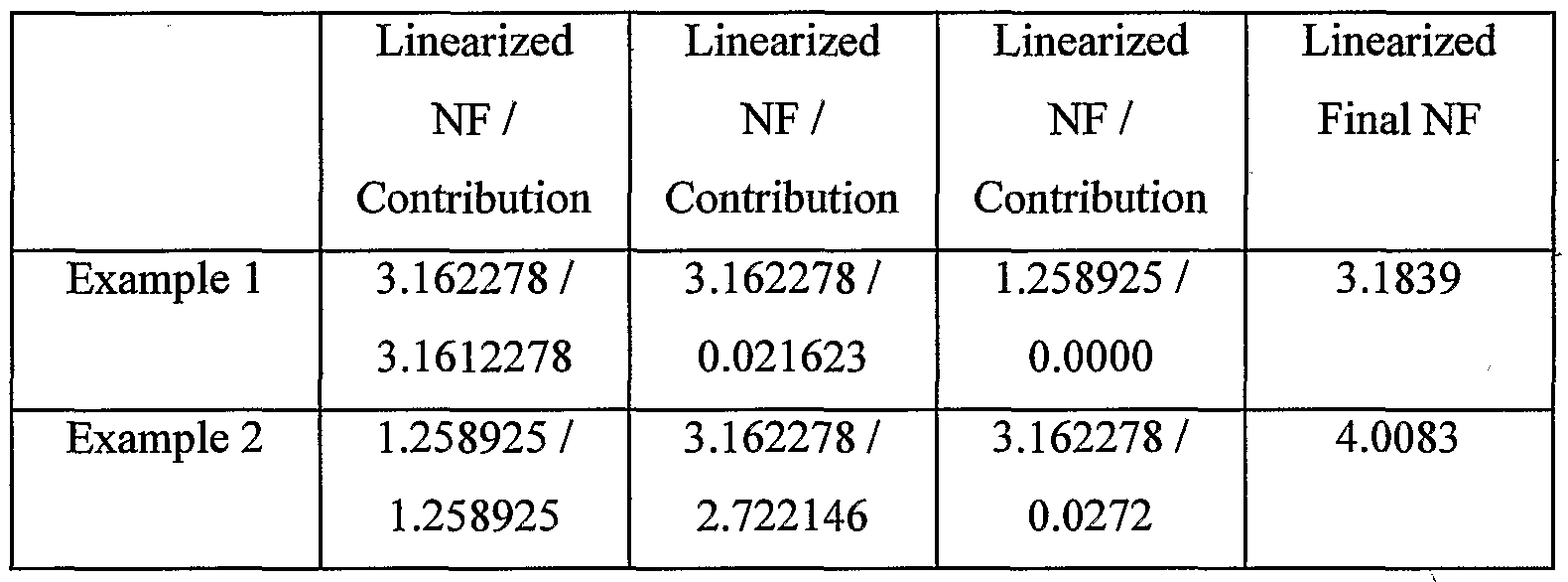
- the gain and noise figures for the two examples 110, 130, respectively can be calculated using example values as shown in the following tables. Since the equalizer is frequency dependent, two frequency points are shown.
- the final noise figure (dB) and distortion values (i.e., composite triple beat (CTB) and composite second order (CSO)) can also be calculated using the values above, and are illustrated in the following table:
- Example 2 the noise figure in Example 2 is worse than the noise figure of Example 1 due to the placement of the equalizer 125.
- the distortion figures in Example 2 are better than Example 1.
- output specifications e.g., output power, distortion levels, and noise figures
- an equalizer may produce better distortion levels, but disadvantageously provide worse noise figures. Therefore, what is needed is an optimum product that is designed for mitigating the effects of the signal loss while maintaining good distortion levels.
- FIG. 1 illustrates equalizers that may be placed either before or after an amplifier chain depending upon design.
- FIG. 2 illustrates a device comprising an equalizer and an amplification chain packaged in an integrated circuit in accordance with the present invention.
- FIG. 3 is a schematic of a single-ended up-tilt equalizer in accordance with the present invention.
- FIG. 4 is a schematic of a single-ended down-tilt equalizer in accordance with the present invention.
- FIG. 5 is a schematic of a differential up-tilt equalizer in accordance with the present invention.
- FIG. 6 is a schematic of a differential down-tilt equalizer in accordance with the present invention.
- the present invention will be described more fully hereinafter with reference to the accompanying drawings in which like numerals represent like elements throughout the several figures, and in which an exemplary embodiment of the invention is shown.
- This invention may, however, be embodied in many different forms and should not be construed as being limited to the embodiments set forth herein; rather, the embodiments are provided so that this disclosure will be thorough and complete, and will fully convey the scope of the invention to those skilled in the art.
- the present invention is described more fully hereinbelow.
- the present invention is suitable for use in a broadband communications system that requires amplification and equalization of transmitted signals due to loss in the transmission channel. More specifically, the present invention comprises an equalizer and an amplification chain that are included within an integrated circuit.
- FIG. 2 illustrates a device comprising an equalizer and an amplification chain packaged in an integrated circuit in accordance with the present invention.
- a signal having an input power level is provided to a first amplification stage 210, which may be included in a transmitting and/ or receiving device.
- An integrated equalizer 215 then corrects for the signal loss, but also attenuates the signal.
- a second amplification stage 220 then amplifies the signal again to provide a signal having a desired output power level.
- the gain and noise figures for the two examples 110, 130, and the present invention, respectively can be calculated using example values as shown in the following tables.
- the final noise figure (dB) and distortion values (i.e., composite triple beat (CTB) and composite second order (CSO)) can also be calculated using the values above, and are illustrated in the following table:
- the equalizer 215 and amplifier stages 210, 220 can alternatively be individually packaged as an integrated circuit and then placed in the arrangement as shown in FIG. 2.
- the amplifier stages 210, 220 can be either single-ended or differential amplifiers. In the case of single-ended amplifiers 210, 220, a single-ended equalizer having either an up-tilt or a down-tilt, depending upon the design of the system, is placed between the amplifiers 210, 220.
- FIG. 3 is a schematic of a single-ended up-tilt equalizer 300 in accordance with the present invention.
- An up-tilt equalizer 300 is used to adjust the signal response upward in frequency since the cable presents losses to the signal.
- the value of the up- tilt equalizer 300 is such that at the input of the next receiver, the incoming signal is a shape that the system requires (e.g., up-tilt, down-tilt, cable, linear, cable/linear, flat, smile, or frown).
- Resonators 305, 310 adjust the frequency response of the signal upward to the point that is necessary to adjust for the cable loss.
- Breakpoints 315, 320 are also in the design for frequency shaping; for example, there may be portions of the signal throughout the frequency band that need leveling.
- FIG. 4 is a schematic of a single-ended down-tilt equalizer 400 in accordance with the present invention.
- the down-tilt equalizer 400 which may also be known in the art as a cable simulator, is used in a receiving device when there is not a sufficient length of cable at the input of the transmitting device or the output of the receiving device to sufficiently level an up-tilted signal.
- the down-tilt equalizer 400 also uses breakpoints, resonators, and an impedance match with values depending on the system design. It will be appreciated that the single-ended equalizers 300, 400 use ground as a reference.
- FIGs. 5 and 6 are schematics of a differential up-tilt equalizer 500 and a down-tilt equalizer 600, respectively, in accordance with the present invention. Similar to the single-ended equalizers 300, 400, the differential equalizers have breakpoints, resonators, and impedance match networks with values chosen for an intended value equalizer.
- the differential equalizers 500, 600 have several advantages when used between or after a differential amplifier stage. A first advantage is that there is symmetry in the differential input and output lines.
- the differential equalizer 500, 600 designed using integrated circuit technology has balance and symmetry that is required to improve CSO; whereas, conventional component equalizers have too much variance and could potentially unbalance the differential lines in a complex equalizer design. A design with unbalanced differential legs will degrade the CSO performance.
- Another advantage is the reduced circuit complexity that is achieved by not having to go from a differential output to a single-ended input and then a single-ended output to a differential input. Having a differential equalizer reduces the total part costs and design time.
- a differential equalizer 500, 600 provides a floating ground in contrast to a single-ended equalizer 300, 400. The floating ground allows an increased bandwidth and lower loss capability. More specifically, the differential lines reference to either signal, not to ground.
Abstract
Description


Claims
Priority Applications (1)
| Application Number | Priority Date | Filing Date | Title |
|---|---|---|---|
| EP05740094A EP1738459A1 (en) | 2004-04-16 | 2005-04-15 | A device including an equalizer and an amplification chain for broadband integrated circuit applications |
Applications Claiming Priority (2)
| Application Number | Priority Date | Filing Date | Title |
|---|---|---|---|
| US10/825,994 | 2004-04-16 | ||
| US10/825,994 US20050232346A1 (en) | 2004-04-16 | 2004-04-16 | Device including an equalizer and an amplification chain for broadband integrated circuit applications |
Publications (1)
| Publication Number | Publication Date |
|---|---|
| WO2005104353A1 true WO2005104353A1 (en) | 2005-11-03 |
Family
ID=34967202
Family Applications (1)
| Application Number | Title | Priority Date | Filing Date |
|---|---|---|---|
| PCT/US2005/012988 WO2005104353A1 (en) | 2004-04-16 | 2005-04-15 | A device including an equalizer and an amplification chain for broadband integrated circuit applications |
Country Status (3)
| Country | Link |
|---|---|
| US (1) | US20050232346A1 (en) |
| EP (1) | EP1738459A1 (en) |
| WO (1) | WO2005104353A1 (en) |
Families Citing this family (3)
| Publication number | Priority date | Publication date | Assignee | Title |
|---|---|---|---|---|
| US8558636B2 (en) * | 2007-03-30 | 2013-10-15 | Intel Corporation | Package embedded equalizer |
| CN101534162B (en) * | 2009-04-16 | 2013-08-28 | 华为终端有限公司 | Method and system for measuring noise coefficient |
| CN114650025A (en) * | 2022-05-24 | 2022-06-21 | 合肥芯谷微电子有限公司 | Negative slope equalizer with high equalization volume, high linearity and high return loss |
Citations (11)
| Publication number | Priority date | Publication date | Assignee | Title |
|---|---|---|---|---|
| US3883830A (en) * | 1974-05-13 | 1975-05-13 | Hekimian Laboratories Inc | Line conditioner with independent gain and delay control |
| US3938056A (en) * | 1971-01-18 | 1976-02-10 | Teledyne, Inc. | Method and apparatus for enhancing the output from a traveling wave tube |
| US4266204A (en) * | 1979-09-04 | 1981-05-05 | Sperry Rand Corporation | Delay line signal equalizer for magnetic recording signal detection circuits |
| US4489281A (en) * | 1982-03-30 | 1984-12-18 | Nippon Electric Co., Ltd. | Automatic gain control amplifier left at an optimum gain after an end of a digital input signal |
| US6160452A (en) * | 1998-07-23 | 2000-12-12 | Adc Telecommunications, Inc. | Circuits and methods for a monitoring circuit in a network amplifier |
| EP1098435A1 (en) * | 1999-11-03 | 2001-05-09 | Space Systems / Loral, Inc. | Low cost miniature broadband linearizer |
| US20020097114A1 (en) * | 1999-02-16 | 2002-07-25 | Yoshiaki Nakano | Spurious signal reduction circuit |
| US6433642B1 (en) * | 2000-07-19 | 2002-08-13 | Trw Inc. | Impedance matched frequency dependent gain compensation network for multi-octave passband equalization |
| US6721427B1 (en) * | 1999-06-08 | 2004-04-13 | Zanden Audio System Co., Ltd. | Analog filter for digital audio system and audio amplifier for using the same |
| US6788169B1 (en) * | 1999-12-29 | 2004-09-07 | Broadband Royalty Corporation | Amplifier composite triple beat (CTB) reduction by phase filtering |
| US6836184B1 (en) * | 1999-07-02 | 2004-12-28 | Adc Telecommunications, Inc. | Network amplifier with microprocessor control |
-
2004
- 2004-04-16 US US10/825,994 patent/US20050232346A1/en not_active Abandoned
-
2005
- 2005-04-15 EP EP05740094A patent/EP1738459A1/en not_active Withdrawn
- 2005-04-15 WO PCT/US2005/012988 patent/WO2005104353A1/en not_active Application Discontinuation
Patent Citations (11)
| Publication number | Priority date | Publication date | Assignee | Title |
|---|---|---|---|---|
| US3938056A (en) * | 1971-01-18 | 1976-02-10 | Teledyne, Inc. | Method and apparatus for enhancing the output from a traveling wave tube |
| US3883830A (en) * | 1974-05-13 | 1975-05-13 | Hekimian Laboratories Inc | Line conditioner with independent gain and delay control |
| US4266204A (en) * | 1979-09-04 | 1981-05-05 | Sperry Rand Corporation | Delay line signal equalizer for magnetic recording signal detection circuits |
| US4489281A (en) * | 1982-03-30 | 1984-12-18 | Nippon Electric Co., Ltd. | Automatic gain control amplifier left at an optimum gain after an end of a digital input signal |
| US6160452A (en) * | 1998-07-23 | 2000-12-12 | Adc Telecommunications, Inc. | Circuits and methods for a monitoring circuit in a network amplifier |
| US20020097114A1 (en) * | 1999-02-16 | 2002-07-25 | Yoshiaki Nakano | Spurious signal reduction circuit |
| US6721427B1 (en) * | 1999-06-08 | 2004-04-13 | Zanden Audio System Co., Ltd. | Analog filter for digital audio system and audio amplifier for using the same |
| US6836184B1 (en) * | 1999-07-02 | 2004-12-28 | Adc Telecommunications, Inc. | Network amplifier with microprocessor control |
| EP1098435A1 (en) * | 1999-11-03 | 2001-05-09 | Space Systems / Loral, Inc. | Low cost miniature broadband linearizer |
| US6788169B1 (en) * | 1999-12-29 | 2004-09-07 | Broadband Royalty Corporation | Amplifier composite triple beat (CTB) reduction by phase filtering |
| US6433642B1 (en) * | 2000-07-19 | 2002-08-13 | Trw Inc. | Impedance matched frequency dependent gain compensation network for multi-octave passband equalization |
Also Published As
| Publication number | Publication date |
|---|---|
| EP1738459A1 (en) | 2007-01-03 |
| US20050232346A1 (en) | 2005-10-20 |
Similar Documents
| Publication | Publication Date | Title |
|---|---|---|
| US8995932B2 (en) | Transmitter noise suppression in receiver | |
| US9054782B2 (en) | Methods for canceling interfering wireless signals in cable customer premises equipment devices and outside plant | |
| US20160308562A1 (en) | Digital suppression of transmitter intermodulation in receiver | |
| US20070096830A1 (en) | Wideband circuits and methods | |
| US8774747B2 (en) | Radio frequency receiver | |
| WO2013008117A1 (en) | Electronic duplexer | |
| KR101625727B1 (en) | Current buffer | |
| US6326848B1 (en) | Circuits and methods for monitoring a signal in a network | |
| EP1738459A1 (en) | A device including an equalizer and an amplification chain for broadband integrated circuit applications | |
| KR20050006207A (en) | Full duplexing for power line data communications | |
| US9374115B2 (en) | Method, base station and apparatus in a base station for reducing intermodulation distortion | |
| US4370624A (en) | Low noise amplifier circuit with reduced low-frequency gain | |
| EP1741201A1 (en) | A differential equalizer for broadband communications systems | |
| US7978011B1 (en) | Systems and methods for mitigating distortion in single-ended amplifiers | |
| EP3367580A1 (en) | Transmission arrangement for full-duplex communication | |
| US8238848B2 (en) | Feed forward noise reduction in a transmitter | |
| US10084618B2 (en) | Processing circuit and signal correction method | |
| KR101878875B1 (en) | Apparatus and method for clibration of transmitter in communication device | |
| CN211702041U (en) | Optimization system for receiving background noise in optical fiber transmission link | |
| CN112398507B (en) | Noise signal processing device and method | |
| KR101003001B1 (en) | Power output unit for an optical communication and telecommunication equipments | |
| CN202353599U (en) | Adjacent-channel interference restraining circuit for microwave transceivers | |
| KR200393485Y1 (en) | Noise damping amplifier for cable television and internet network | |
| RU2019036C1 (en) | Predistortion corrector | |
| KR101522546B1 (en) | Equalizer Circuit Using ATT PAD |
Legal Events
| Date | Code | Title | Description |
|---|---|---|---|
| AK | Designated states |
Kind code of ref document: A1 Designated state(s): AE AG AL AM AT AU AZ BA BB BG BR BW BY BZ CA CH CN CO CR CU CZ DE DK DM DZ EC EE EG ES FI GB GD GE GH GM HR HU ID IL IN IS JP KE KG KM KP KR KZ LC LK LR LS LT LU LV MA MD MG MK MN MW MX MZ NA NI NO NZ OM PG PH PL PT RO RU SC SD SE SG SK SL SM SY TJ TM TN TR TT TZ UA UG US UZ VC VN YU ZA ZM ZW |
|
| AL | Designated countries for regional patents |
Kind code of ref document: A1 Designated state(s): GM KE LS MW MZ NA SD SL SZ TZ UG ZM ZW AM AZ BY KG KZ MD RU TJ TM AT BE BG CH CY CZ DE DK EE ES FI FR GB GR HU IE IS IT LT LU MC NL PL PT RO SE SI SK TR BF BJ CF CG CI CM GA GN GQ GW ML MR NE SN TD TG |
|
| 121 | Ep: the epo has been informed by wipo that ep was designated in this application | ||
| NENP | Non-entry into the national phase |
Ref country code: DE |
|
| WWW | Wipo information: withdrawn in national office |
Country of ref document: DE |
|
| WWE | Wipo information: entry into national phase |
Ref document number: 2005740094 Country of ref document: EP |
|
| WWP | Wipo information: published in national office |
Ref document number: 2005740094 Country of ref document: EP |
|
| WWW | Wipo information: withdrawn in national office |
Ref document number: 2005740094 Country of ref document: EP |