WO2009018509A1 - Thin film transistors using thin film semiconductor materials - Google Patents

Thin film transistors using thin film semiconductor materials Download PDF

Info

Publication number
WO2009018509A1
WO2009018509A1 PCT/US2008/071890 US2008071890W WO2009018509A1 WO 2009018509 A1 WO2009018509 A1 WO 2009018509A1 US 2008071890 W US2008071890 W US 2008071890W WO 2009018509 A1 WO2009018509 A1 WO 2009018509A1
Authority
WO
WIPO (PCT)
Prior art keywords
semiconductor layer
oxygen
nitrogen
layer
mobility
Prior art date
Application number
PCT/US2008/071890
Other languages
French (fr)
Inventor
Yan Ye
Original Assignee
Applied Materials, Inc.
Priority date (The priority date is an assumption and is not a legal conclusion. Google has not performed a legal analysis and makes no representation as to the accuracy of the date listed.)
Filing date
Publication date
Application filed by Applied Materials, Inc. filed Critical Applied Materials, Inc.
Priority to EP08797025A priority Critical patent/EP2183780A4/en
Priority to KR1020157012165A priority patent/KR101603180B1/en
Priority to KR1020107004741A priority patent/KR101536101B1/en
Priority to CN2008801062915A priority patent/CN101803028B/en
Priority to JP2010520218A priority patent/JP5718052B2/en
Publication of WO2009018509A1 publication Critical patent/WO2009018509A1/en

Links

Classifications

    • HELECTRICITY
    • H01ELECTRIC ELEMENTS
    • H01LSEMICONDUCTOR DEVICES NOT COVERED BY CLASS H10
    • H01L29/00Semiconductor devices adapted for rectifying, amplifying, oscillating or switching, or capacitors or resistors with at least one potential-jump barrier or surface barrier, e.g. PN junction depletion layer or carrier concentration layer; Details of semiconductor bodies or of electrodes thereof  ; Multistep manufacturing processes therefor
    • H01L29/66Types of semiconductor device ; Multistep manufacturing processes therefor
    • H01L29/68Types of semiconductor device ; Multistep manufacturing processes therefor controllable by only the electric current supplied, or only the electric potential applied, to an electrode which does not carry the current to be rectified, amplified or switched
    • H01L29/76Unipolar devices, e.g. field effect transistors
    • H01L29/772Field effect transistors
    • H01L29/78Field effect transistors with field effect produced by an insulated gate
    • H01L29/786Thin film transistors, i.e. transistors with a channel being at least partly a thin film
    • H01L29/7869Thin film transistors, i.e. transistors with a channel being at least partly a thin film having a semiconductor body comprising an oxide semiconductor material, e.g. zinc oxide, copper aluminium oxide, cadmium stannate
    • HELECTRICITY
    • H01ELECTRIC ELEMENTS
    • H01LSEMICONDUCTOR DEVICES NOT COVERED BY CLASS H10
    • H01L27/00Devices consisting of a plurality of semiconductor or other solid-state components formed in or on a common substrate
    • H01L27/02Devices consisting of a plurality of semiconductor or other solid-state components formed in or on a common substrate including semiconductor components specially adapted for rectifying, oscillating, amplifying or switching and having at least one potential-jump barrier or surface barrier; including integrated passive circuit elements with at least one potential-jump barrier or surface barrier
    • H01L27/12Devices consisting of a plurality of semiconductor or other solid-state components formed in or on a common substrate including semiconductor components specially adapted for rectifying, oscillating, amplifying or switching and having at least one potential-jump barrier or surface barrier; including integrated passive circuit elements with at least one potential-jump barrier or surface barrier the substrate being other than a semiconductor body, e.g. an insulating body
    • H01L27/1214Devices consisting of a plurality of semiconductor or other solid-state components formed in or on a common substrate including semiconductor components specially adapted for rectifying, oscillating, amplifying or switching and having at least one potential-jump barrier or surface barrier; including integrated passive circuit elements with at least one potential-jump barrier or surface barrier the substrate being other than a semiconductor body, e.g. an insulating body comprising a plurality of TFTs formed on a non-semiconducting substrate, e.g. driving circuits for AMLCDs
    • H01L27/1222Devices consisting of a plurality of semiconductor or other solid-state components formed in or on a common substrate including semiconductor components specially adapted for rectifying, oscillating, amplifying or switching and having at least one potential-jump barrier or surface barrier; including integrated passive circuit elements with at least one potential-jump barrier or surface barrier the substrate being other than a semiconductor body, e.g. an insulating body comprising a plurality of TFTs formed on a non-semiconducting substrate, e.g. driving circuits for AMLCDs with a particular composition, shape or crystalline structure of the active layer
    • H01L27/1225Devices consisting of a plurality of semiconductor or other solid-state components formed in or on a common substrate including semiconductor components specially adapted for rectifying, oscillating, amplifying or switching and having at least one potential-jump barrier or surface barrier; including integrated passive circuit elements with at least one potential-jump barrier or surface barrier the substrate being other than a semiconductor body, e.g. an insulating body comprising a plurality of TFTs formed on a non-semiconducting substrate, e.g. driving circuits for AMLCDs with a particular composition, shape or crystalline structure of the active layer with semiconductor materials not belonging to the group IV of the periodic table, e.g. InGaZnO
    • HELECTRICITY
    • H01ELECTRIC ELEMENTS
    • H01LSEMICONDUCTOR DEVICES NOT COVERED BY CLASS H10
    • H01L29/00Semiconductor devices adapted for rectifying, amplifying, oscillating or switching, or capacitors or resistors with at least one potential-jump barrier or surface barrier, e.g. PN junction depletion layer or carrier concentration layer; Details of semiconductor bodies or of electrodes thereof  ; Multistep manufacturing processes therefor
    • H01L29/66Types of semiconductor device ; Multistep manufacturing processes therefor
    • H01L29/66007Multistep manufacturing processes
    • H01L29/66075Multistep manufacturing processes of devices having semiconductor bodies comprising group 14 or group 13/15 materials
    • H01L29/66227Multistep manufacturing processes of devices having semiconductor bodies comprising group 14 or group 13/15 materials the devices being controllable only by the electric current supplied or the electric potential applied, to an electrode which does not carry the current to be rectified, amplified or switched, e.g. three-terminal devices
    • H01L29/66409Unipolar field-effect transistors
    • H01L29/66477Unipolar field-effect transistors with an insulated gate, i.e. MISFET
    • H01L29/66742Thin film unipolar transistors

Definitions

  • Embodiments of the present invention generally relate to field effect transistors (FETs) and thin film transistors (TFTs) having semiconductor materials comprising oxygen, nitrogen, and one or more elements selected from the group consisting of zinc, gallium, cadmium, indium, and tin.
  • FETs field effect transistors
  • TFTs thin film transistors
  • LCDs liquid crystal active matrix displays
  • OLEDs organic light emitting diodes
  • TFTs made with amorphous silicon have become the key components of the flat panel display industry.
  • amorphous silicon does have its limitations such as low mobility.
  • the mobility required for OLEDs is at least 10 times higher than that achievable with amorphous silicon.
  • the deposition temperature for amorphous silicon may be high, which can cause a Vth shift.
  • a high current may be necessary for amorphous silicon, which can lead to stability issues in OLEDs.
  • Polysilicon on the other hand, has a higher mobility than amorphous silicon. Polysilicon is crystalline, which leads to non-uniform deposition. Due to the limitations of amorphous silicon, OLED advancement has been difficult.
  • Zinc oxide is a compound semiconductor that can be grown as a crystalline material at relatively low deposition temperatures on various substrates such as glass and plastic. Zinc oxide based TFTs may not degrade upon exposure to visible light. Therefore, a shield layer, as is necessary for silicon based TFTs, is not present. Without the shield layer, the TFT remains transparent. Zinc oxide, while having a mobility greater than amorphous silicon, still has a low mobility.
  • the present invention generally comprises TFTs having semiconductor material comprising oxygen, nitrogen, and one or more element selected from the group consisting of zinc, tin, gallium, cadmium, and indium as the active channel.
  • the semiconductor material may be used in bottom gate TFTs, top gate TFTs, and other types of TFTs.
  • the TFTs may be patterned by etching to create both the channel and the metal electrodes.
  • the source-drain electrodes may be defined by dry etching using the semiconductor material as an etch stop layer.
  • the active layer carrier concentration, mobility, and interface with other layers of the TFT can be tuned to predetermined values. The tuning may be accomplished by changing the nitrogen containing gas to oxygen containing gas flow ratio, annealing and/or plasma treating the deposited semiconductor film, or changing the concentration of aluminum doping.
  • a TFT comprises a semiconductor layer comprising oxygen, nitrogen and one or more elements selected from the group consisting of zinc, indium, tin, cadmium, gallium, and combinations thereof.
  • a TFT fabrication method comprises depositing a semiconductor layer over a substrate, the semiconductor layer comprising oxygen, nitrogen and one or more elements selected from the group consisting of zinc, indium, tin, cadmium, gallium, and combinations thereof.
  • a TFT fabrication method comprises depositing a semiconductor layer over a substrate, the semiconductor layer comprising oxygen, nitrogen and one or more elements selected from the group consisting of an element having filled s and d orbitals, an element having a filled f orbital, and combinations thereof.
  • the method also includes depositing a source-drain electrode layer over the active channel layer, first etching the source-drain electrode layer and the active channel layer to create an active channel, and second etching the source-drain electrode layer to define source-drain electrodes.
  • Figure 1 is a schematic cross sectional view of a PVD chamber according to one embodiment of the invention.
  • Figures 2A-2E are XRD graphs for films showing the formation of zinc and zinc oxide peaks as a function of oxygen gas flow.
  • Figures 3A-3F are XRD graphs for showing the formation of a semiconductor film according at various nitrogen gas flow rates according to one embodiment of the invention.
  • Figures 4A-4G show a process sequence for forming a bottom gate TFT according to one embodiment of the invention.
  • Figure 5 is a schematic cross sectional view of an etch stop TFT according to one embodiment of the invention.
  • Figure 6 is a schematic cross sectional view of a top gate TFT according to one embodiment of the invention.
  • Figure 7 is a schematic view of an active-matrix LCD according to one embodiment of the invention.
  • Figure 8 is a schematic view of an active-matrix OLED according to one embodiment of the invention.
  • Figures 9A-9C show the Vth for various active channel lengths and widths.
  • Figures 10A-10C show a comparision of the Vth for active channels having a common length and width.
  • the present invention generally comprises TFTs having semiconductor material comprising oxygen, nitrogen, and one or more element selected from the group consisting of zinc, tin, gallium, cadmium, and indium as the active channel.
  • the semiconductor material may be used in bottom gate TFTs, top gate TFTs, and other types of TFTs.
  • the TFTs may be patterned by etching to create both the channel and the metal electrodes. Then, the source-drain electrodes may be defined by dry etching using the semiconductor material as an etch stop layer.
  • the active layer carrier concentration, mobility, and interface with other layers of the TFT can be tuned to predetermined values.
  • the tuning may be accomplished by changing the nitrogen containing gas to oxygen containing gas flow ratio, annealing and/or plasma treating the deposited semiconductor film, or changing the concentration of aluminum doping.
  • the semiconductor film comprising nitrogen, oxygen, and one or more elements selected from zinc, indium, gallium, cadmium, and tin may be deposited by reactive sputtering.
  • the reactive sputtering method is illustratively described and may be practiced in a PVD chamber for processing large area substrates, such as a 4300 PVD chamber, available from AKT America, Inc., a subsidiary of Applied Materials, Inc., Santa Clara, California.
  • the semiconductor film produced according to the method may be determined by the film structure and composition
  • the reactive sputtering method may have utility in other system configurations, including those systems configured to process large area round substrates and those systems produced by other manufacturers, including roll-to-roll process platforms.
  • the invention is illustratively described below as deposited by PVD, other methods including chemical vapor deposition (CVD), atomic layer deposition (ALD), or spin-on processes may be utilized to deposit the inventive films.
  • FIG. 1 is a cross-sectional schematic view of a PVD chamber 100 according to one embodiment of the invention.
  • the chamber 100 may be evacuated by a vacuum pump 114.
  • a substrate 102 may be disposed opposite a target 104.
  • the substrate may be disposed on a susceptor 106 within the chamber 100.
  • the susceptor 106 may be elevated and lowered as shown by arrows "A" by an actuator 112.
  • the susceptor 106 may be elevated to raise the substrate 102 to a processing position and lowered so that the substrate 102 may be removed from the chamber 100.
  • Lift pins 108 elevate the substrate 102 above the susceptor 106 when the susceptor 106 is in the lowered position.
  • Grounding straps 110 may ground the susceptor 106 during processing.
  • the susceptor 106 may be raised during processing to aid in uniform deposition.
  • the target 104 may comprise one or more targets 104.
  • the target 104 may comprise a large area sputtering target 104.
  • the target 104 may comprise a plurality of tiles.
  • the target 104 may comprise a plurality of target strips.
  • the target 104 may comprise one or more cylindrical, rotary targets.
  • the target 104 may be bonded to a backing plate 116 by a bonding layer (not shown).
  • One or more magnetrons 118 may be disposed behind the backing plate 116. The magnetrons 118 may scan across the backing plate 116 in a linear movement or in a two dimensional path.
  • the walls of the chamber may be shielded from deposition by a dark space shield 120 and a chamber shield 122.
  • an anode 124 may be placed between the target 104 and the substrate 102.
  • the anode 124 may be bead blasted stainless steel coated with arc sprayed aluminum.
  • one end of the anode 124 may be mounted to the chamber wall by a bracket 130.
  • the anode 124 provides a charge in opposition to the target 104 so that charged ions will be attracted thereto rather than to the chamber walls which are typically at ground potential.
  • a cooling fluid may be provided through the one or more anodes 124.
  • flaking of material from the anodes 124 may be reduced.
  • the anodes 124 spanning the processing space may not be necessary as the chamber walls may be sufficient to provide a path to ground and a uniform plasma distribution.
  • One or more gas introduction tubes 126 may also span the distance across the chamber 100 between the target 104 and the substrate 102. For smaller substrates and hence, smaller chambers, the gas introduction tubes 126 spanning the processing space may not be necessary as an even gas distribution may be possible through conventional gas introduction means.
  • the gas introduction tubes 126 may introduce sputtering gases from a gas panel 132.
  • the gas introduction tubes 126 may be coupled with the anodes 124 by one or more couplings 128.
  • the coupling 128 may be made of thermally conductive material to permit the gas introduction tubes 126 to be conductively cooled. Additionally, the coupling 128 may be electrically conductive as well so that the gas introduction tubes 126 are grounded and function as anodes.
  • the reactive sputtering process may comprise disposing a metallic sputtering target opposite a substrate in a sputtering chamber.
  • the metallic sputtering target may substantially comprise one or more elements selected from the group consisting of zinc, gallium, indium, tin, and cadmium.
  • the sputtering target may comprise one or more elements having a filled s orbital and a filled d orbital.
  • the sputtering target may comprise one or more elements having a filled f orbital.
  • the sputtering target may comprise one or more divalent elements.
  • the sputtering target may comprise one or more trivalent elements.
  • the sputtering target may comprise one or more tetravalent elements.
  • the sputtering target may also comprise a dopant. Suitable dopants that may be used include Al, Sn, Ga, Ca, Si, Ti, Cu, Ge, In, Ni, Mn, Cr, V, Mg, Si x N y , AI x O y , and SiC. In one embodiment, the dopant comprises aluminum. In another embodiment, the dopant comprises tin.
  • the substrate on the other hand, may comprise plastic, paper, polymer, glass, stainless steel, and combinations thereof. When the substrate is plastic, the reactive sputtering may occur at temperatures below about 180 degrees Celsius.
  • Examples of semiconductor films that may be deposited include ZnO x N y :AI, ZnO x N y :Sn, SnO x N y :AI, lnO x N y :AI, lnO x N y :Sn, CdO x N y :AI, CdO x N y :Sn, GaO x N y :AI, GaO x N y :Sn, ZnSnO x N y :AI ZnlnO x N y :AI, ZnlnO x N y :Sn, ZnCdO x N y :AI, ZnCdO x N y :Sn, ZnGaO x N y :AI, ZnGaO x N y :Sn, SnlnO x N y :AI, SnCdO x N y :AI, SnGa
  • argon, a nitrogen containing gas, and an oxygen containing gas may be provided to the chamber for reactive sputtering the metallic target. Additional additives such as B 2 H 6 , CO 2 , CO, CH 4 , and combinations thereof may also be provided to the chamber during the sputtering.
  • the nitrogen containing gas comprises N 2 .
  • the nitrogen containing gas comprises N 2 O, NH 3 , or combinations thereof.
  • the oxygen containing gas comprises O 2 .
  • the oxygen containing gas comprises N 2 O.
  • the nitrogen of the nitrogen containing gas and the oxygen of the oxygen containing gas react with the metal from the sputtering target to form a semiconductor material comprising metal, oxygen, nitrogen, and optionally a dopant on the substrate.
  • the nitrogen containing gas and the oxygen containing gas are separate gases.
  • the nitrogen containing gas and the oxygen containing gas comprise the same gas.
  • the film deposited is a semiconductor film.
  • semiconductor films that may be deposited include ZnO x N y , SnO x Ny, InO x N y , CdO x N y , GaO x N y , ZnSnO x Ny, ZnInO x Ny, ZnCdO x Ny, ZnGaO x N y , SnInO x N y , SnCdO x N y , SnGaO x N y , InCdO x Ny, InGaO x Ny, CdGaO x Ny, ZnSnInO x N y , ZnSnCdO x N y , ZnSnGaO x N y , ZnInCdO x Ny, ZnInGaO x Ny, ZnCdGaO x N y , SnInCdO x N y ,
  • the semiconductor film may comprise an oxynitride compound.
  • the semiconductor film comprises both a metal oxynitride compound as well as a metal nitride compound.
  • the semiconductor film may comprise a metal oxynitride compound, a metal nitride compound, and a metal oxide compound.
  • the semiconductor film may comprise a metal oxynitride compound and a metal oxide compound.
  • the semiconductor film may comprise a metal nitride compound and a metal oxide compound.
  • the ratio of the nitrogen containing gas to the oxygen containing gas may affect the mobility, carrier concentration, and resistivity of the semiconductor film.
  • Table I shows the effect of the nitrogen flow rate on the mobility, resistivity, and carrier concentration for a tin target sputtered in an atmosphere of argon and nitrogen gas. Generally, Table I shows that when the nitrogen flow rate increases, the mobility also increases. The argon and oxygen flow rates may remain the same. In Table I, the argon flow rate is 60 seem and the oxygen flow rate is 5 seem. The higher substrate temperature also provides an increase in mobility. The carrier concentration is weakly correlated with the mobility.
  • the deposited film is an n-type semiconductor material which may function as an electron carrier and hence, the carrier concentration is shown as a negative number.
  • the oxygen containing gas also affects the mobility, carrier concentration, and resistivity of the semiconductor film.
  • Table Il shows the effect of the oxygen flow rate on the mobility, resistivity, and carrier concentration for a tin target sputtered in an atmosphere of argon, nitrogen gas, and oxygen gas.
  • the argon flow rate may remain the same.
  • the argon flow rate is 60 seem.
  • Table Il shows that for high nitrogen gas to oxygen gas ratios, the mobility may be higher than the mobility for amorphous silicon. Additionally, the higher the ratio of nitrogen to oxygen, the lower the carrier concentration. At a 200 seem nitrogen flow rate, the mobility increases as the oxygen flow rate increase, but then decreases at higher oxygen flow rates.
  • the mobility may be between about 4 cm 2 /V-s and about 10 cm 2 /V-s at a temperature of 150 degrees Celsius.
  • the increase in mobility is not correlated to the carrier concentration.
  • the mobility improvement may be a result of less scattering of the carrier.
  • the mobility may be very low if no nitrogen additives are used. In such a scenario, the carrier concentration drops significantly as the oxygen gas flow increases. The higher the substrate temperature for a tin target, the better the mobility.
  • the pressure may be between about 5 mTorr to about 20 mTorr.
  • the amount of dopant may also affect the mobility of the deposited film. However, the mobility will still generally increase with an increase of nitrogen gas flow whether the target is doped or not.
  • Table III shows the effect of dopant upon the mobility, carrier concentration, and resistivity. The dopant is shown in weight percentage. The argon flow rate may be the same for each deposited film. In Table III, the argon flow rate is 120 seem. The carrier concentration when utilizing a dopant may be lower than in the scenario where no dopant is used. Thus, the dopant may be used to tune the carrier concentration. Table
  • Table IV discloses the effect of oxygen gas flow on the mobility, carrier concentration, and resistivity of the semiconductor film.
  • the mobility of the film will increase as the oxygen flow increases, but drop with a further increase in oxygen flow rate.
  • the argon flow rate may be the same for each deposited film. In Table IV, the argon flow rate is 120 seem.
  • the mobility of the film will decrease once the nitrogen containing gas to oxygen containing gas ratio is less than about 10:1.
  • the increase in mobility does not relate to an increase in carrier concentration as the oxygen flow rate increases.
  • the carrier concentration and mobility may be tuned with the amount of dopant present.
  • Table V shows the affect of the power density applied on the mobility, carrier concentration, and resistivity of the semiconductor film. Generally, the power density does not greatly affect the mobility, but the higher the power density, the higher the carrier concentration and resistivity. In one embodiment, the power density applied to the sputtering target may be between about 0.3 W/cm 2 and about l .O W/cm 2 . Table V
  • Table Vl shows the effects of utilizing N 2 O as the oxygen containing gas in depositing the semiconductor film.
  • the N 2 O gas is effective as an oxygen containing gas in raising the mobility of the semiconductor film and producing a reasonably low carrier concentration.
  • Table VII shows the chemical analysis for a semiconductor film that comprises tin, oxygen, and nitrogen and shows the effect of oxygen containing gas upon the film using X-ray photoelectron spectroscopy (XPS).
  • Film 1 was deposited by sputtering a tin target for 360 seconds while a DC bias of 400 W was applied to the sputtering target.
  • Argon was introduced to the processing chamber at a flow rate of 60 seem, nitrogen was introduced at a flow rate of 200 seem, and oxygen was introduced at a flow rate of 5 seem. The deposition occurred at a temperature of 250 degrees Celsius.
  • Film 1 had a carbon content of Film 1 was 22.5 atomic percent, a nitrogen content of 19.4 atomic percent, an oxygen content of 29.4 atomic percent, a fluorine content of 0.7 atomic percent, and a tin content of 28.1 atomic percent. Most, if not all, of the carbon could arise from adventitious carbon (i.e., carbon compounds adsorbed onto the surface of any sample exposed to the atmosphere).
  • Film 2 was deposited by sputtering a tin target for 360 seconds while a DC bias of 400 W was applied to the sputtering target.
  • Argon was introduced to the processing chamber at a flow rate of 60 seem, nitrogen was introduced at a flow rate of 200 seem, and oxygen was introduced at a flow rate of 20 seem.
  • Film 2 had a carbon content of 17.3 atomic percent, a nitrogen content of 4.5 atomic percent, an oxygen content of 49.9 atomic percent, a fluorine content of 0.6 percent, and a tin content of 27.7 atomic percent. Most, if not all, of the carbon could arise from adventitious carbon (i.e., carbon compounds adsorbed onto the surface of any sample exposed to the atmosphere). As shown in Table VII, as the oxygen flow rate (and hence, the ratio of oxygen to nitrogen) increases, the oxynitride content increases as well as does the tin oxide content. However, the tin nitride content and silicon oxynitride content is reduced. In Table VII, R equals oxygen or nitrogen.
  • Table VIII shows the results for several semiconductor films that were deposited by sputtering.
  • the semiconductor films comprised zinc, tin, oxygen, and nitrogen.
  • the semiconductor films were sputter deposited from a sputtering target having a zinc content of 70 atomic percent and a tin content of 30 atomic percent.
  • the deposition occurred at a temperature of 250 degrees Celsius with a power of 400 W applied to the sputtering target.
  • the deposition occurred for 360 seconds under an argon flow rate of 60 seem and an oxygen flow rate of 20 seem.
  • the data shows that the mobility of the semiconductor film increases as the nitrogen flow rate (and hence, the ratio of nitrogen gas to oxygen gas) increases.
  • the amount of oxygen may be selected so that the amount of oxygen is not sufficient to completely oxidize the zinc to form zinc oxide. If the amount of oxygen containing gas supplied is too high, the mobility of the film may not be sufficient because the film may be too oxidized.
  • the amount of oxidation of zinc may affect the transmittance. For example, completely oxidized zinc may have a transmittance of greater than about 80 percent.
  • One manner of determining the desired oxygen flow is to run a reactive sputtering process using argon and oxygen gases without using nitrogen gas. Experiments may be performed at different oxygen flow rates and the optical transmittance in the visible wavelength may be measured.
  • the desired oxygen flow may be just before the film has a maximum transparency that may be achieved.
  • Table IX shows the optical transmittance for zinc oxide reactively sputter deposited at various oxygen flow rates.
  • the maximum preferred transmittance may be 80 percent. In other embodiments, the maximum transmittance may not be 80 percent if the glass absorption or light interference is included.
  • the experiments may be useful when using different DC target power, different substrate temperature, or even different oxygen containing gases such as N 2 O.
  • Another method to determine the desired oxygen gas flow is to perform the reactive sputtering to form zinc oxide under the condition of providing no nitrogen or a low amount of nitrogen as discussed above and then measure the sheet resistance.
  • An oxygen flow rate that produces a sheet resistance between about 100 ohm/sq and 1.0 x 10 7 ohm/sq may be the desired oxygen flow rate.
  • Figures 2A-2E are XRD graphs for films showing the formation of zinc and zinc oxide peaks as a function of oxygen gas flow. Each of the films shown in Figures 2A-2E were deposited at an argon flow rate of 600 sccm/m 3 and 1 ,000W and various oxygen flow rates.
  • Figure 2A shows an XRD graph of a film formed when no oxygen gas is provided during the sputtering.
  • Several zinc peaks were produced having various intensities.
  • a zinc (002) peak is shown for 2 theta (i.e., the angle between the incident x-ray and the detector of the diffractometer) between about 35.5 and 37 with an intensity of about 625 counts.
  • a zinc (100) peak is shown between about 38 and 40 with an intensity of about 450 counts.
  • a zinc (101) peak is shown between about 42.5 and 44 with an intensity of about 1050 counts.
  • a zinc (102) peak is shown between about 53 and 55 with an intensity of about 325 counts.
  • a zinc (103) peak is shown between about 69.5 and 70 with an intensity of about 300.
  • a zinc peak (110) peak is shown between about 70 and 71 with an intensity of about 275 counts.
  • the ratio of peak heights for the zinc (002) : zinc (100) : zinc (101) : zinc (102) : zinc (103) : zinc (110) is about 2.27:1.64:3.82:1.182:1.091 :1. All peaks are marked using the International Center for Diffraction Data (ICDD) PDF2 database (rev. 2004) for phase identification.
  • ICDD International Center for Diffraction Data
  • the zinc peaks diminish in intensity as shown in Figure 2B.
  • the zinc (002) peak diminishes to about 500 counts.
  • the zinc (100) peak diminishes to about 375 counts.
  • the zinc (101) peak diminishes to about 750 counts.
  • the zinc (102) peak diminishes to about 250 counts.
  • the zinc (110) peak diminishes to about 225 counts, and the zinc (103) peak is not present.
  • the ratio of the peak heights for zinc (002) : zinc (100) : zinc (101) : zinc (102) : zinc (110) is about 2.22:1.67:3.33:1.11 :1.
  • the amount of oxygen supplied should be less than about 150 sccm/m 3 because at 150 sccm/m 3 a strong zinc oxide peak appears. It is to be understood that the flow rate of oxygen is proportional to the chamber size. Thus, for as the size of the chamber increases, the oxygen flow rate may also increase. Similarly, as the size of the chamber is reduced, the oxygen flow rate may decrease.
  • Figures 3A-3F are XRD graphs for showing the formation of a semiconductor film according at various nitrogen gas flow rates according to one embodiment of the invention. Each of the films shown in Figures 3A-3F were deposited at an argon flow rate of 600 sccm/m 3 , 2,00OW, an oxygen flow rate of 100 sccm/m 3 , and various nitrogen flow rates.
  • Figure 3A shows an XRD graph of a film deposited with no nitrogen.
  • the graph reveals several strong peaks including a peak between about 35 and about 37 of zinc oxide (101) and zinc (002) having an intensity of about 575 counts, a peak between about 38 and 40 of zinc (100) having an intensity of about 380 counts, and a peak between about 42.5 and 44 of zinc (101) having an intensity of about 700 counts.
  • Smaller peaks of zinc oxide (002) between about 35.5 and 37 with an intensity of about 390 counts, zinc (102) between about 53 and 55 with an intensity of about 275 counts, zinc (103) between about 69.5 and 70 with an intensity of about 225 counts, and a peak of zinc (110) between about 70 and 71 with an intensity of about 225 counts are also present.
  • the ratio of the peak heights for zinc oxide (101 ) : zinc (002) : zinc (100) : zinc (101) : zinc oxide (002) : zinc (102) : zinc (103) : zinc (110) is about 2.55:2.55:1.24:3.11 :1.73:1.22:1 :1.
  • a first peak of Zn 3 N 2 (222) has formed between about 31 and 33 with an intensity of about 2050 counts.
  • a second peak of Zn 3 N 2 (411 ) has formed between about 35 and 42 with an intensity of about 1850 counts.
  • the ratio of peak heights for Zn 3 N 2 (222) : Zn 3 N 2 (411 ) is about 1.11 :1.
  • the ratio of peak heights for Zn 3 N 2 (222) : Zn 3 N 2 (411) is about 0.96:1.
  • the Zn 3 N 2 (222) peak and the Zn 3 N 2 (411 ) weaken to about 2350 and 2050 respectively, but a new peak of Zn 3 N 2 (400) develops between about 36 and 37.5 with an intensity of about 1700 counts as shown in Figure 3F.
  • the ratio of peak heights for Zn 3 N 2 (222) : Zn 3 N 2 (411 ) : Zn 3 N 2 (400) is about 1.38:1.21 :1.
  • the amount of nitrogen supplied should be greater than about 300 sccm/m 3 because at 300 sccm/m 3 the zinc oxide peaks diminish significantly such that essentially no zinc oxide is present in the film. It is to be understood that the flow rate of nitrogen is proportional to the chamber size. Thus, as the size of the chamber increases, the nitrogen flow rate may also increase. Similarly, as the size of the chamber is reduced, the nitrogen flow rate may decrease.
  • the new semiconductor film discussed herein may be deposited under a nitrogen to oxygen flow rate ratio of greater than about 2:1.
  • the flow ratio of nitrogen to oxygen may be 10:1 to about 50:1. In still another embodiment, the flow ratio of nitrogen to oxygen may be 20:1.
  • the flow rate of the nitrogen containing gas may be much greater than the flow rate of the oxygen containing gas as discussed above.
  • the deposited semiconductor material may have a mobility greater than amorphous silicon.
  • Table X shows the mobility as a function of nitrogen gas flow rate according to one embodiment of the invention.
  • Films deposited under conditions of 200 sccm/m 3 oxygen had a mobility of about 1 cm 2 /V-s for a nitrogen flow rate of 1 ,500 sccm/m 3 and a mobility of about 10 cm 2 /V-s for a nitrogen flow rate of 2,500 sccm/m 3 .
  • Films deposited under conditions of 250 sccm/m 3 oxygen has a mobility of about 5 cm 2 /V-s for a nitrogen flow rate of 500 sccm/m 3 , about 2 cm 2 /V-s for a nitrogen flow rate of 1 ,500 sccm/m 3 , and about 12 cm 2 /V-s for a nitrogen flow rate of 2,500 sccm/m 3 .
  • the mobility of the films was markedly increased over the films deposited at oxygen flow rates of 25 sccm/m 3 and below and films deposited at oxygen flow rates of 200 sccm/m 3 and above. Additionally, the films deposited with an oxygen flow rate of between 50 sccm/m 3 and 150 sccm/m 3 have mobilities far greater than amorphous silicon. At nitrogen flow rates of between 1 ,000 sccm/m 3 and 2,500 sccm/m 3 , the mobility of the films were, in most cases, higher than 22 cm 2 /V-s.
  • the semiconductor films containing zinc, oxygen, and nitrogen have a significant improvement in mobility.
  • nitrogen to oxygen gas flow ratios of about 10:1 to about 50:1 may produce semiconductor films having mobility greater than 20 times the mobility of amorphous silicon and 2 times the mobility of polysilicon. It is to be understood that while the table shows specific flow rates of nitrogen gas and oxygen gas, the flow rates of the oxygen gas and nitrogen gas are relative to the chamber size and thus, are scalable to account for different chamber sizes.
  • Table Xl shows the sheet resistance, carrier concentration, and resistivity as a function of nitrogen gas flow rate according to one embodiment of the invention.
  • the sheet resistance of the semiconductor layer comprising zinc, oxygen, and nitrogen may be between about 100 ohm/sq and about 10,000 ohm/sq.
  • the electron carrier concentration lowers. Consequently, the resistivity increases.
  • Annealing may also significantly raise the mobility of the semiconductor film containing zinc, oxygen, and nitrogen.
  • Table XII shows the mobility as a function of nitrogen gas flow rate after annealing according to one embodiment of the invention. After annealing, the mobility may be greater than 50 cm 2 /V-s. In one embodiment, the mobility may be increased to greater than 90 cm 2 /V-s by annealing. The annealing may occur for about five minutes in a nitrogen atmosphere at a temperature of about 400 degrees Celsius.
  • the amount of dopant may also affect the mobility of the semiconductor film containing zinc, nitrogen, and oxygen.
  • Tables XIII and XIV show the mobility, sheet resistance, carrier concentration, and resistivity for various nitrogen and oxygen flow rates when reactively sputtering a zinc sputtering target that is doped with aluminum.
  • the amount of dopant in the sputtering target may be tuned to ensure a predetermined mobility, sheet resistance, carrier concentration, and resistivity are achieved.
  • Table XIV [0059] The temperature of the susceptor may also influence the mobility of the semiconductor film.
  • Table XV shows the mobility, sheet resistance, carrier concentration, and resistivity for various nitrogen flow rates in sputtering a zinc sputtering target at temperatures of 30 degrees Celsius, 50 degrees Celsius, and 95 degrees Celsius.
  • the reactive sputtering may effectively form a semiconductor film having mobility higher than amorphous silicon and polysilicon at temperatures significantly below 400 degrees Celsius, including temperatures approaching room temperature.
  • the semiconductor film may have a higher mobility than amorphous silicon.
  • the film deposited according to the above discussed deposition techniques may comprise a ternary compound semiconductor material having zinc, nitrogen, and oxygen such as ZnN x Oy.
  • the ternary compound semiconductor material may be doped such as ZnN x O y :AI.
  • the ternary semiconductor compound may have a high mobility and a low electron carrier density when deposited at room temperature in contrast to zinc oxide which has a high electron mobility and a high electron carrier density.
  • the ternary compound has a mobility higher than 30 cm 2 /V-cm and an electron carrier density lower than 1.0e+19 #/cc.
  • the mobility When the film is annealed at about 400 degrees Celsius, the mobility may be increased to greater than 100 cm 2 /V-cm and the electron carrier density may be lower than 1.0e+18 #/cc without changing the film crystallographic orientation and composition.
  • the high mobility and low electron density may be achieved for the ternary compound even when the film is an amorphous compound or poorly oriented crystallographic compound.
  • the optical band gap of the ternary compound may also be improved compared to zinc oxide.
  • Zinc oxide typically has a band gap of about 3.2 eV.
  • the ternary compound comprising zinc, nitrogen, and oxygen may have a band gap from about 3.1 eV to about 1.2 eV.
  • the band gap may be adjusted by altering the deposition parameters such as nitrogen to oxygen flow ratio, power density, pressure, annealing, and deposition temperature. Due to the lower band gap, the ternary compound may be useful for photovoltaic devices and other electronic devices.
  • the ternary film may be converted to p-type or n-type semiconductor material.
  • the annealing or plasma treatment may be fine tuned without fundamentally changing the compound structure and chemical composition. The fine tuning permits the properties of the compound to be tailored to meet the performance requirements of devices in which the compound may be used.
  • the ternary compound may be useful as a transparent semiconductor layer in a TFT device, a compound layer in a photovoltaic device or solar panel, or as a compound layer in a sensor device.
  • Figures 4A-4G show a process sequence for forming a bottom gate TFT 400 according to one embodiment of the invention.
  • the TFT may comprise a substrate 402.
  • the substrate 402 may comprise glass.
  • the substrate 402 may comprise a polymer.
  • the substrate may comprise plastic.
  • the substrate may comprise metal.
  • a gate electrode 404 may be formed over the substrate.
  • the gate electrode 404 may comprise an electrically conductive layer that controls the movement of charge carriers within the TFT.
  • the gate electrode 404 may comprise a metal such as aluminum, tungsten, chromium, tantalum, or combinations thereof.
  • the gate electrode 404 may be formed using conventional deposition techniques including sputtering, lithography, and etching.
  • a gate dielectric layer 406 may be deposited.
  • the gate dielectric layer 406 may comprise silicon dioxide, silicon oxynitride, silicon nitride, or combinations thereof.
  • the gate dielectric layer 406 may be deposited by well known deposition techniques including plasma enhanced chemical vapor deposition (PECVD).
  • PECVD plasma enhanced chemical vapor deposition
  • the active channel 408 (i.e., semiconductor layer) may be formed as shown in Figure 4B.
  • the active channel 408 is annealed.
  • the active channel 408 is exposed to a plasma treatment.
  • the annealing and/or plasma treatment may increase the mobility of the active channel 408.
  • the active channel 408 may comprise the ternary compound having zinc, oxygen, and nitrogen as discussed above.
  • the ternary compound is doped with aluminum.
  • the source-drain layer 410 may comprise a metal such as aluminum, tungsten, molybdenum, chromium, tantalum, and combinations thereof. In order to define the active channel 408 and the source-drain electrodes, both the source-drain layer 410 and the active channel 408 may be etched.
  • a mask 412 may be disposed on the source-drain layer 410.
  • the mask 412 may have a predetermined pattern.
  • the mask 412 may be disposed on the source-drain layer 410 by conventional techniques including photoresist deposition followed by pattern development.
  • the active channel 408 and the source-drain layer 410 may be simultaneously etched as shown in Figure 4E.
  • Figure 4F shows a top view of Figure 4E.
  • the active channel 408 may be exposed by the etching.
  • the active channel 408 may be exposed by wet etching both the source-drain layer 410 and a portion of the active channel 408.
  • the source-drain layer 410 may be dry etched followed by a wet etching of a portion of the active channel 408.
  • the source-drain layer 410 may be etched without etching the active channel 408.
  • the dry etching may be performed with a gas containing an element selected from chlorine, oxygen, fluorine, or combinations thereof.
  • source-drain electrodes may be defined by dry etching the source-drain layer 410 using the active channel 408 as an etch stop layer.
  • Figure 4G shows a top view of the exposed active channel 408 and defined source electrode 414 and drain electrode 416.
  • the active channel 408 may function as an etch stop layer during dry plasma etching because the ternary compound comprising zinc, oxygen, and nitrogen (and in certain embodiments, aluminum) may not be effectively etched by plasma.
  • Figure 5 is a schematic cross sectional view of an etch stop TFT 500 according to one embodiment of the invention.
  • the etch stop TFT may comprise a substrate 502, a gate electrode 504, and a gate dielectric layer 506.
  • the etch stop TFT 500 is similar to the bottom gate TFT shown above in Figures 4A-4G, but an etch stop 510 may be present over the active channel 508 between the source electrode 512 and the drain electrode 514.
  • the materials for the substrate 502, gate electrode 504, gate dielectric 506, active channel 508, source electrode 512, and drain electrode 514 may be as described above in relation to the bottom gate TFT.
  • the etch stop 510 may comprise a dielectric material comprising silicon and one or more of oxygen and nitrogen.
  • FIG. 6 is a schematic cross sectional view of a top gate TFT 600 according to one embodiment of the invention.
  • the top gate TFT 600 may comprise a substrate 602 having a light shielding layer 604 deposited thereon.
  • a dielectric layer 606 may be deposited over the light shielding layer 604.
  • a source electrode 608 and a drain electrode 610 may be deposited over the dielectric layer 606.
  • the active channel layer 612 may be deposited over the source electrode 608 and the drain electrode 610.
  • a gate dielectric layer 614 may be deposited over the active channel 612 and the gate electrode 616 may be deposited over the gate dielectric layer 614.
  • the materials for the substrate 602, gate electrode 616, gate dielectric 614, active channel 612, source electrode 608, and drain electrode 610 may be as described above in relation to the bottom gate TFT.
  • the channel and electrode contact area may be formed by wet etching or dry etching followed by wet etching. Then, the contact area may be defined by dry etching using the active channel as an etch stop layer.
  • FIG. 7 is a schematic view of an active-matrix LCD 700 according to one embodiment of the invention.
  • Figure 7 shows a TFT substrate and a color filter substrate with a liquid crystal material sandwiched therebetween.
  • the TFT controls a current to the pixel electrode creating an electric field to control the orientation of the liquid crystal material and thus the amount of light that is transmitted through the color filter.
  • the TFTs are arranged in a matrix on a glass substrate. To address a particular pixel, the proper row is switched on, and then a charge is sent down the correct column. Since all of the other rows that the column intersects are turned off, only the capacitor at the designated pixel receives a charge. The capacitor is able to hold the charge until the next refresh cycle. If the amount of voltage supplied to a crystal is controlled, the crystal may untwist only enough to allow some light through.
  • the active matrix LCD 700 shown in Figure 7 may be controlled by a TFT 714.
  • the TFT 714 may turn pixels on or off.
  • the LCD 700 may comprise a bonding pad 706, a pixel electrode 708, a storage capacitor 728, a polarizer 702, a substrate 704, an alignment layer 710, a spacer 712, a short 716, a seal 718, a black matrix 720, a color filter 724, and a common electrode 724.
  • FIG 8 is a schematic view of an active-matrix OLED 800 according to one embodiment of the invention.
  • Figure 8 shows a TFT controlling the amount of current applied to the emissive organic layers of the OLED.
  • Active-matrix OLEDs have full layers of cathode, organic molecules and anode, but the anode layer overlays a TFT array that forms a matrix.
  • the TFT array itself is the circuitry that determines which pixels get turned on to form an image.
  • Active-matrix OLEDs consume less power than passive-matrix OLEDs because the TFT array requires less power than external circuitry, so they are efficient for large displays.
  • Active- matrix OLEDs also have faster refresh rates suitable for video.
  • Active-matrix OLEDs may be used in computer monitors, large screen TVs, electronic signs, and electronic billboards.
  • the OLED 800 may be controlled by a TFT 802 that turns the pixels on or off.
  • the OLED 800 comprises a TFT 802, an anode 804, a hole injection layer 806, an ionization layer 808, a buffer layer 810, a transparent cathode 812, an emissive layer 814, and an encapsulation layer 816.
  • Figures 9A-9C show the Vth for various active channel lengths and widths.
  • Figure 9A shows the Vth for a active channel length of 40 ⁇ m and a width of
  • Figure 9B shows the Vth for a active channel length of 80 ⁇ m and a width of
  • Figure 9C shows the Vth for a active channel length of 80 ⁇ m and a width of 20 ⁇ m. In each of Figures 9A-9C, it is shown that the ternary compound active layer has a high on-off ratio and a high current.
  • Figures 10A-10C show a comparision of the Vth for active channels having a common length and width.
  • the active channel width is 40 ⁇ m and the width is 10 ⁇ m.
  • Figure 10A is the Vth for amorphous silicon.
  • Figure 10B is the ternary compound without annealing.
  • Figure 10C is the ternary compound after annealing.
  • the annealed film in Figure 10C is even better.
  • the annealed film has a high saturation current as compared to the non-annealed film.
  • the annealed film is about 100 times better than the amorphous silicon.
  • the performance of the TFTs described above can be adjusted or tuned by changing the active layer carrier concentration, the active layer mobility, and the characteristics of the active layer at the interface with other layers.
  • the TFTs may be tuned by changing the nitrogen containing gas flow rate during the film deposition.
  • the ratio of the nitrogen containing gas to the oxygen containing gas used in sputter deposition of the active layer may affect the mobility, carrier concentration, and other factors.
  • a user may set a predetermined value for the carrier concentration, the mobility, or other characteristic and then adjust the nitrogen to oxygen flow ratio accordingly to produce the desired film properties. The adjustment may even occur in response to an in situ measurement to permit real time control of the deposition process.
  • the TFTs may also be tuned by the amount of aluminum doping.
  • the amount of aluminum doping may be predetermined so that a sputtering target of appropriate composition may be disposed within the processing chamber.
  • the TFTs may be tuned by annealing and/or plasma treating the active layer after deposition or during integration with other films. As noted above, heat treating the ternary compound may increase the mobility of the film.
  • TFTs comprising oxygen, nitrogen, and one or more elements selected from the group consisting of zinc, tin, gallium, indium, and cadmium have increased mobility over TFTs made with amorphous silicon.
  • the increased mobility of the TFTs permits the TFTs to be used not only for LCDs, but also for the next generation of displays, OLEDs.

Abstract

The present invention generally comprises TFTs having semiconductor material comprising oxygen, nitrogen, and one or more element selected from the group consisting of zinc, tin, gallium, cadmium, and indium as the active channel. The semiconductor material may be used in bottom gate TFTs, top gate TFTs, and other types of TFTs. The TFTs may be patterned by etching to create both the channel and the metal electrodes. Then, the source-drain electrodes may be defined by dry etching using the semiconductor material as an etch stop layer. The active layer carrier concentration, mobility, and interface with other layers of the TFT can be tuned to predetermined values. The tuning may be accomplished by changing the nitrogen containing gas to oxygen containing gas flow ratio, annealing and/or plasma treating the deposited semiconductor film, or changing the concentration of aluminum doping.

Description

THIN FILM TRANSISTORS USING THIN FILM SEMICONDUCTOR MATERIALS
BACKGROUND OF THE INVENTION Field of the Invention
[0001] Embodiments of the present invention generally relate to field effect transistors (FETs) and thin film transistors (TFTs) having semiconductor materials comprising oxygen, nitrogen, and one or more elements selected from the group consisting of zinc, gallium, cadmium, indium, and tin.
Description of the Related Art
[0002] Current interest in TFT arrays is particularly high because these devices may be used in liquid crystal active matrix displays (LCDs) of the kind often employed for computer and television flat panels. The LCDs may also contain light emitting diodes (LEDs) for back lighting. Further, organic light emitting diodes (OLEDs) have been used for active matrix displays, and these OLEDs require TFTs for addressing the activity of the displays.
[0003] TFTs made with amorphous silicon have become the key components of the flat panel display industry. Unfortunately amorphous silicon does have its limitations such as low mobility. The mobility required for OLEDs is at least 10 times higher than that achievable with amorphous silicon. The deposition temperature for amorphous silicon may be high, which can cause a Vth shift. A high current may be necessary for amorphous silicon, which can lead to stability issues in OLEDs. Polysilicon, on the other hand, has a higher mobility than amorphous silicon. Polysilicon is crystalline, which leads to non-uniform deposition. Due to the limitations of amorphous silicon, OLED advancement has been difficult.
[0004] In recent years, transparent TFTs have been created in which zinc oxide has been used as the active channel layer. Zinc oxide is a compound semiconductor that can be grown as a crystalline material at relatively low deposition temperatures on various substrates such as glass and plastic. Zinc oxide based TFTs may not degrade upon exposure to visible light. Therefore, a shield layer, as is necessary for silicon based TFTs, is not present. Without the shield layer, the TFT remains transparent. Zinc oxide, while having a mobility greater than amorphous silicon, still has a low mobility.
[0005] Therefore, there is a need in the art for TFTs having transparent active channels with high mobility.
SUMMARY OF THE INVENTION
[0006] The present invention generally comprises TFTs having semiconductor material comprising oxygen, nitrogen, and one or more element selected from the group consisting of zinc, tin, gallium, cadmium, and indium as the active channel. The semiconductor material may be used in bottom gate TFTs, top gate TFTs, and other types of TFTs. The TFTs may be patterned by etching to create both the channel and the metal electrodes. Then, the source-drain electrodes may be defined by dry etching using the semiconductor material as an etch stop layer. The active layer carrier concentration, mobility, and interface with other layers of the TFT can be tuned to predetermined values. The tuning may be accomplished by changing the nitrogen containing gas to oxygen containing gas flow ratio, annealing and/or plasma treating the deposited semiconductor film, or changing the concentration of aluminum doping.
[0007] In one embodiment, a TFT is disclosed. The transistor comprises a semiconductor layer comprising oxygen, nitrogen and one or more elements selected from the group consisting of zinc, indium, tin, cadmium, gallium, and combinations thereof. In another embodiment, a TFT fabrication method is disclosed. The method comprises depositing a semiconductor layer over a substrate, the semiconductor layer comprising oxygen, nitrogen and one or more elements selected from the group consisting of zinc, indium, tin, cadmium, gallium, and combinations thereof.
[0008] In another embodiment, a TFT fabrication method is disclosed. The method comprises depositing a semiconductor layer over a substrate, the semiconductor layer comprising oxygen, nitrogen and one or more elements selected from the group consisting of an element having filled s and d orbitals, an element having a filled f orbital, and combinations thereof. The method also includes depositing a source-drain electrode layer over the active channel layer, first etching the source-drain electrode layer and the active channel layer to create an active channel, and second etching the source-drain electrode layer to define source-drain electrodes.
BRIEF DESCRIPTION OF THE DRAWINGS
[0009] So that the manner in which the above recited features of the present invention can be understood in detail, a more particular description of the invention, briefly summarized above, may be had by reference to embodiments, some of which are illustrated in the appended drawings. It is to be noted, however, that the appended drawings illustrate only typical embodiments of this invention and are therefore not to be considered limiting of its scope, for the invention may admit to other equally effective embodiments.
[0010] Figure 1 is a schematic cross sectional view of a PVD chamber according to one embodiment of the invention.
[0011] Figures 2A-2E are XRD graphs for films showing the formation of zinc and zinc oxide peaks as a function of oxygen gas flow.
[0012] Figures 3A-3F are XRD graphs for showing the formation of a semiconductor film according at various nitrogen gas flow rates according to one embodiment of the invention.
[0013] Figures 4A-4G show a process sequence for forming a bottom gate TFT according to one embodiment of the invention.
[0014] Figure 5 is a schematic cross sectional view of an etch stop TFT according to one embodiment of the invention. [0015] Figure 6 is a schematic cross sectional view of a top gate TFT according to one embodiment of the invention.
[0016] Figure 7 is a schematic view of an active-matrix LCD according to one embodiment of the invention.
[0017] Figure 8 is a schematic view of an active-matrix OLED according to one embodiment of the invention.
[0018] Figures 9A-9C show the Vth for various active channel lengths and widths.
[0019] Figures 10A-10C show a comparision of the Vth for active channels having a common length and width.
[0020] To facilitate understanding, identical reference numerals have been used, where possible, to designate identical elements that are common to the figures. It is contemplated that elements disclosed in one embodiment may be beneficially utilized on other embodiments without specific recitation.
DETAILED DESCRIPTION
[0021] The present invention generally comprises TFTs having semiconductor material comprising oxygen, nitrogen, and one or more element selected from the group consisting of zinc, tin, gallium, cadmium, and indium as the active channel. The semiconductor material may be used in bottom gate TFTs, top gate TFTs, and other types of TFTs. The TFTs may be patterned by etching to create both the channel and the metal electrodes. Then, the source-drain electrodes may be defined by dry etching using the semiconductor material as an etch stop layer. The active layer carrier concentration, mobility, and interface with other layers of the TFT can be tuned to predetermined values. The tuning may be accomplished by changing the nitrogen containing gas to oxygen containing gas flow ratio, annealing and/or plasma treating the deposited semiconductor film, or changing the concentration of aluminum doping. [0022] The semiconductor film comprising nitrogen, oxygen, and one or more elements selected from zinc, indium, gallium, cadmium, and tin may be deposited by reactive sputtering. The reactive sputtering method is illustratively described and may be practiced in a PVD chamber for processing large area substrates, such as a 4300 PVD chamber, available from AKT America, Inc., a subsidiary of Applied Materials, Inc., Santa Clara, California. However, because the semiconductor film produced according to the method may be determined by the film structure and composition, it should be understood that the reactive sputtering method may have utility in other system configurations, including those systems configured to process large area round substrates and those systems produced by other manufacturers, including roll-to-roll process platforms. It is to be understood that while the invention is illustratively described below as deposited by PVD, other methods including chemical vapor deposition (CVD), atomic layer deposition (ALD), or spin-on processes may be utilized to deposit the inventive films.
[0023] Figure 1 is a cross-sectional schematic view of a PVD chamber 100 according to one embodiment of the invention. The chamber 100 may be evacuated by a vacuum pump 114. Within the chamber 100, a substrate 102 may be disposed opposite a target 104. The substrate may be disposed on a susceptor 106 within the chamber 100. The susceptor 106 may be elevated and lowered as shown by arrows "A" by an actuator 112. The susceptor 106 may be elevated to raise the substrate 102 to a processing position and lowered so that the substrate 102 may be removed from the chamber 100. Lift pins 108 elevate the substrate 102 above the susceptor 106 when the susceptor 106 is in the lowered position. Grounding straps 110 may ground the susceptor 106 during processing. The susceptor 106 may be raised during processing to aid in uniform deposition.
[0024] The target 104 may comprise one or more targets 104. In one embodiment, the target 104 may comprise a large area sputtering target 104. In another embodiment, the target 104 may comprise a plurality of tiles. In yet another embodiment, the target 104 may comprise a plurality of target strips. In still another embodiment, the target 104 may comprise one or more cylindrical, rotary targets. The target 104 may be bonded to a backing plate 116 by a bonding layer (not shown). One or more magnetrons 118 may be disposed behind the backing plate 116. The magnetrons 118 may scan across the backing plate 116 in a linear movement or in a two dimensional path. The walls of the chamber may be shielded from deposition by a dark space shield 120 and a chamber shield 122.
[0025] To help provide uniform sputtering deposition across a substrate 102, an anode 124 may be placed between the target 104 and the substrate 102. In one embodiment, the anode 124 may be bead blasted stainless steel coated with arc sprayed aluminum. In one embodiment, one end of the anode 124 may be mounted to the chamber wall by a bracket 130. The anode 124 provides a charge in opposition to the target 104 so that charged ions will be attracted thereto rather than to the chamber walls which are typically at ground potential. By providing the anode 124 between the target 104 and the substrate 102, the plasma may be more uniform, which may aid in the deposition. To reduce flaking, a cooling fluid may be provided through the one or more anodes 124. By reducing the amount of expansion and contraction of the anodes 124, flaking of material from the anodes 124 may be reduced. For smaller substrates and hence, smaller processing chambers, the anodes 124 spanning the processing space may not be necessary as the chamber walls may be sufficient to provide a path to ground and a uniform plasma distribution.
[0026] For reactive sputtering, it may be beneficial to provide a reactive gas into the chamber 100. One or more gas introduction tubes 126 may also span the distance across the chamber 100 between the target 104 and the substrate 102. For smaller substrates and hence, smaller chambers, the gas introduction tubes 126 spanning the processing space may not be necessary as an even gas distribution may be possible through conventional gas introduction means. The gas introduction tubes 126 may introduce sputtering gases from a gas panel 132. The gas introduction tubes 126 may be coupled with the anodes 124 by one or more couplings 128. The coupling 128 may be made of thermally conductive material to permit the gas introduction tubes 126 to be conductively cooled. Additionally, the coupling 128 may be electrically conductive as well so that the gas introduction tubes 126 are grounded and function as anodes.
[0027] The reactive sputtering process may comprise disposing a metallic sputtering target opposite a substrate in a sputtering chamber. The metallic sputtering target may substantially comprise one or more elements selected from the group consisting of zinc, gallium, indium, tin, and cadmium. In one embodiment, the sputtering target may comprise one or more elements having a filled s orbital and a filled d orbital. In another embodiment, the sputtering target may comprise one or more elements having a filled f orbital. In another embodiment, the sputtering target may comprise one or more divalent elements. In another embodiment, the sputtering target may comprise one or more trivalent elements. In still another embodiment, the sputtering target may comprise one or more tetravalent elements.
[0028] The sputtering target may also comprise a dopant. Suitable dopants that may be used include Al, Sn, Ga, Ca, Si, Ti, Cu, Ge, In, Ni, Mn, Cr, V, Mg, SixNy, AIxOy, and SiC. In one embodiment, the dopant comprises aluminum. In another embodiment, the dopant comprises tin. The substrate, on the other hand, may comprise plastic, paper, polymer, glass, stainless steel, and combinations thereof. When the substrate is plastic, the reactive sputtering may occur at temperatures below about 180 degrees Celsius. Examples of semiconductor films that may be deposited include ZnOxNy:AI, ZnOxNy:Sn, SnOxNy:AI, lnOxNy:AI, lnOxNy:Sn, CdOxNy:AI, CdOxNy:Sn, GaOxNy:AI, GaOxNy:Sn, ZnSnOxNy:AI ZnlnOxNy:AI, ZnlnOxNy:Sn, ZnCdOxNy:AI, ZnCdOxNy:Sn, ZnGaOxNy:AI, ZnGaOxNy:Sn, SnlnOxNy:AI, SnCdOxNy:AI, SnGaOxNy:AI, lnCdOxNy:AI, lnCdOxNy:Sn, lnGaOxNy:AI, lnGaOxNy:Sn, CdGaOxNy:AI, CdGaOxNy:Sn, ZnSnlnOxNy:AI, ZnSnCdOxNy:AI, ZnSnGaOxNy:AI, ZnlnCdOxNy:AI, ZnlnCdOxNy:Sn, ZnlnGaOxNy:AI, ZnlnGaOxNy:Sn, ZnCdGaOxNy:AI, ZnCdGaOxNy:Sn, SnlnCdOxNy:AI, SnlnGaOxNy:AI,
SnCdGaOxNy:AI, lnCdGaOxNy:AI, lnCdGaOxNy:Sn, ZnSnlnCdOxNy:AI, ZnSnlnGaOxNy:AI, ZnlnCdGaOxNy:AI, ZnlnCdGaOxNy:Sn, and SnlnCdGaOxNy:AI.
[0029] During the sputtering process, argon, a nitrogen containing gas, and an oxygen containing gas may be provided to the chamber for reactive sputtering the metallic target. Additional additives such as B2H6, CO2, CO, CH4, and combinations thereof may also be provided to the chamber during the sputtering. In one embodiment, the nitrogen containing gas comprises N2. In another embodiment, the nitrogen containing gas comprises N2O, NH3, or combinations thereof. In one embodiment, the oxygen containing gas comprises O2. In another embodiment, the oxygen containing gas comprises N2O. The nitrogen of the nitrogen containing gas and the oxygen of the oxygen containing gas react with the metal from the sputtering target to form a semiconductor material comprising metal, oxygen, nitrogen, and optionally a dopant on the substrate. In one embodiment, the nitrogen containing gas and the oxygen containing gas are separate gases. In another embodiment, the nitrogen containing gas and the oxygen containing gas comprise the same gas.
[0030] The film deposited is a semiconductor film. Examples of semiconductor films that may be deposited include ZnOxNy, SnOxNy, InOxNy, CdOxNy, GaOxNy, ZnSnOxNy, ZnInOxNy, ZnCdOxNy, ZnGaOxNy, SnInOxNy, SnCdOxNy, SnGaOxNy, InCdOxNy, InGaOxNy, CdGaOxNy, ZnSnInOxNy, ZnSnCdOxNy, ZnSnGaOxNy, ZnInCdOxNy, ZnInGaOxNy, ZnCdGaOxNy, SnInCdOxNy, SnInGaOxNy, SnCdGaOxNx, InCdGaOxNy, ZnSnInCdOxNy, ZnSnInGaOxNy, ZnInCdGaOxNy, and SnInCdGaOxNy. Each of the aforementioned semiconductor films may be doped by a dopant.
[0031] The semiconductor film may comprise an oxynitride compound. In one embodiment, the semiconductor film comprises both a metal oxynitride compound as well as a metal nitride compound. In another embodiment, the semiconductor film may comprise a metal oxynitride compound, a metal nitride compound, and a metal oxide compound. In still another embodiment, the semiconductor film may comprise a metal oxynitride compound and a metal oxide compound. In another embodiment, the semiconductor film may comprise a metal nitride compound and a metal oxide compound.
[0032] The ratio of the nitrogen containing gas to the oxygen containing gas may affect the mobility, carrier concentration, and resistivity of the semiconductor film. Table I shows the effect of the nitrogen flow rate on the mobility, resistivity, and carrier concentration for a tin target sputtered in an atmosphere of argon and nitrogen gas. Generally, Table I shows that when the nitrogen flow rate increases, the mobility also increases. The argon and oxygen flow rates may remain the same. In Table I, the argon flow rate is 60 seem and the oxygen flow rate is 5 seem. The higher substrate temperature also provides an increase in mobility. The carrier concentration is weakly correlated with the mobility. The deposited film is an n-type semiconductor material which may function as an electron carrier and hence, the carrier concentration is shown as a negative number.
Table I
Figure imgf000010_0001
[0033] The oxygen containing gas also affects the mobility, carrier concentration, and resistivity of the semiconductor film. Table Il shows the effect of the oxygen flow rate on the mobility, resistivity, and carrier concentration for a tin target sputtered in an atmosphere of argon, nitrogen gas, and oxygen gas. The argon flow rate may remain the same. In Table II, the argon flow rate is 60 seem. Generally, Table Il shows that for high nitrogen gas to oxygen gas ratios, the mobility may be higher than the mobility for amorphous silicon. Additionally, the higher the ratio of nitrogen to oxygen, the lower the carrier concentration. At a 200 seem nitrogen flow rate, the mobility increases as the oxygen flow rate increase, but then decreases at higher oxygen flow rates. In one embodiment, the mobility may be between about 4 cm2/V-s and about 10 cm2/V-s at a temperature of 150 degrees Celsius. The increase in mobility is not correlated to the carrier concentration. Thus, the mobility improvement may be a result of less scattering of the carrier. The mobility may be very low if no nitrogen additives are used. In such a scenario, the carrier concentration drops significantly as the oxygen gas flow increases. The higher the substrate temperature for a tin target, the better the mobility. In one embodiment, the pressure may be between about 5 mTorr to about 20 mTorr.
Table Il
Figure imgf000011_0001
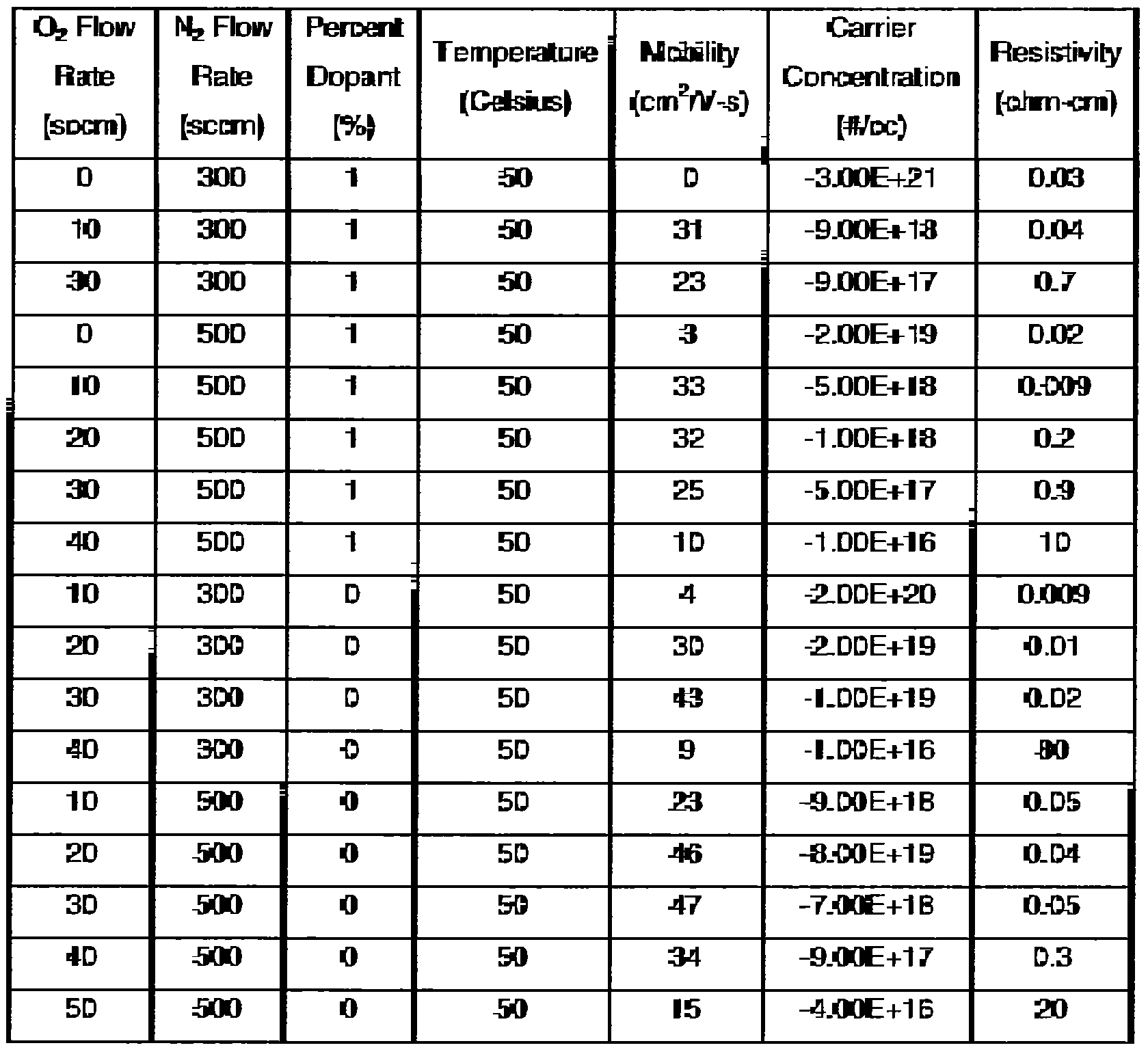
[0034] The amount of dopant may also affect the mobility of the deposited film. However, the mobility will still generally increase with an increase of nitrogen gas flow whether the target is doped or not. Table III shows the effect of dopant upon the mobility, carrier concentration, and resistivity. The dopant is shown in weight percentage. The argon flow rate may be the same for each deposited film. In Table III, the argon flow rate is 120 seem. The carrier concentration when utilizing a dopant may be lower than in the scenario where no dopant is used. Thus, the dopant may be used to tune the carrier concentration. Table
Figure imgf000012_0001
[0035] Table IV discloses the effect of oxygen gas flow on the mobility, carrier concentration, and resistivity of the semiconductor film. Generally, under a fixed nitrogen gas flow, the mobility of the film will increase as the oxygen flow increases, but drop with a further increase in oxygen flow rate. The argon flow rate may be the same for each deposited film. In Table IV, the argon flow rate is 120 seem. In one embodiment, the mobility of the film will decrease once the nitrogen containing gas to oxygen containing gas ratio is less than about 10:1. The increase in mobility does not relate to an increase in carrier concentration as the oxygen flow rate increases. When a dopant is used, the mobility and carrier concentration may be lowered. Thus, the carrier concentration and mobility may be tuned with the amount of dopant present. Table IV
Figure imgf000013_0001
[0036] Table V shows the affect of the power density applied on the mobility, carrier concentration, and resistivity of the semiconductor film. Generally, the power density does not greatly affect the mobility, but the higher the power density, the higher the carrier concentration and resistivity. In one embodiment, the power density applied to the sputtering target may be between about 0.3 W/cm2 and about l .O W/cm2. Table V
Figure imgf000014_0001
[0037] Table Vl shows the effects of utilizing N2O as the oxygen containing gas in depositing the semiconductor film. The N2O gas is effective as an oxygen containing gas in raising the mobility of the semiconductor film and producing a reasonably low carrier concentration.
Table Vl
Figure imgf000015_0001
[0038] Table VII shows the chemical analysis for a semiconductor film that comprises tin, oxygen, and nitrogen and shows the effect of oxygen containing gas upon the film using X-ray photoelectron spectroscopy (XPS). Film 1 was deposited by sputtering a tin target for 360 seconds while a DC bias of 400 W was applied to the sputtering target. Argon was introduced to the processing chamber at a flow rate of 60 seem, nitrogen was introduced at a flow rate of 200 seem, and oxygen was introduced at a flow rate of 5 seem. The deposition occurred at a temperature of 250 degrees Celsius. Film 1 had a carbon content of Film 1 was 22.5 atomic percent, a nitrogen content of 19.4 atomic percent, an oxygen content of 29.4 atomic percent, a fluorine content of 0.7 atomic percent, and a tin content of 28.1 atomic percent. Most, if not all, of the carbon could arise from adventitious carbon (i.e., carbon compounds adsorbed onto the surface of any sample exposed to the atmosphere). Film 2 was deposited by sputtering a tin target for 360 seconds while a DC bias of 400 W was applied to the sputtering target. Argon was introduced to the processing chamber at a flow rate of 60 seem, nitrogen was introduced at a flow rate of 200 seem, and oxygen was introduced at a flow rate of 20 seem. The deposition occurred at a temperature of 250 degrees Celsius. Film 2 had a carbon content of 17.3 atomic percent, a nitrogen content of 4.5 atomic percent, an oxygen content of 49.9 atomic percent, a fluorine content of 0.6 percent, and a tin content of 27.7 atomic percent. Most, if not all, of the carbon could arise from adventitious carbon (i.e., carbon compounds adsorbed onto the surface of any sample exposed to the atmosphere). As shown in Table VII, as the oxygen flow rate (and hence, the ratio of oxygen to nitrogen) increases, the oxynitride content increases as well as does the tin oxide content. However, the tin nitride content and silicon oxynitride content is reduced. In Table VII, R equals oxygen or nitrogen.
Table VII
Figure imgf000017_0001
[0039] Table VIII shows the results for several semiconductor films that were deposited by sputtering. The semiconductor films comprised zinc, tin, oxygen, and nitrogen. The semiconductor films were sputter deposited from a sputtering target having a zinc content of 70 atomic percent and a tin content of 30 atomic percent. The deposition occurred at a temperature of 250 degrees Celsius with a power of 400 W applied to the sputtering target. The deposition occurred for 360 seconds under an argon flow rate of 60 seem and an oxygen flow rate of 20 seem. The data shows that the mobility of the semiconductor film increases as the nitrogen flow rate (and hence, the ratio of nitrogen gas to oxygen gas) increases.
Table VIII
Figure imgf000018_0001
Zinc, oxygen, and nitrogen compounds
[0040] In order to determine the desired oxygen flow rate for forming the semiconductor film comprising zinc, oxygen, and nitrogen, the amount of oxygen may be selected so that the amount of oxygen is not sufficient to completely oxidize the zinc to form zinc oxide. If the amount of oxygen containing gas supplied is too high, the mobility of the film may not be sufficient because the film may be too oxidized. The amount of oxidation of zinc may affect the transmittance. For example, completely oxidized zinc may have a transmittance of greater than about 80 percent. One manner of determining the desired oxygen flow is to run a reactive sputtering process using argon and oxygen gases without using nitrogen gas. Experiments may be performed at different oxygen flow rates and the optical transmittance in the visible wavelength may be measured. The desired oxygen flow may be just before the film has a maximum transparency that may be achieved. Table IX shows the optical transmittance for zinc oxide reactively sputter deposited at various oxygen flow rates. In one embodiment, the maximum preferred transmittance may be 80 percent. In other embodiments, the maximum transmittance may not be 80 percent if the glass absorption or light interference is included. The experiments may be useful when using different DC target power, different substrate temperature, or even different oxygen containing gases such as N2O.
Table IX
Figure imgf000019_0001
[0041] Another method to determine the desired oxygen gas flow is to perform the reactive sputtering to form zinc oxide under the condition of providing no nitrogen or a low amount of nitrogen as discussed above and then measure the sheet resistance. An oxygen flow rate that produces a sheet resistance between about 100 ohm/sq and 1.0 x 10⁷ ohm/sq may be the desired oxygen flow rate.
[0042] Yet another manner for determining the desired oxygen flow rate is to take an XRD film structure measurement. Figures 2A-2E are XRD graphs for films showing the formation of zinc and zinc oxide peaks as a function of oxygen gas flow. Each of the films shown in Figures 2A-2E were deposited at an argon flow rate of 600 sccm/m3 and 1 ,000W and various oxygen flow rates.
[0043] Figure 2A shows an XRD graph of a film formed when no oxygen gas is provided during the sputtering. Several zinc peaks were produced having various intensities. A zinc (002) peak is shown for 2 theta (i.e., the angle between the incident x-ray and the detector of the diffractometer) between about 35.5 and 37 with an intensity of about 625 counts. A zinc (100) peak is shown between about 38 and 40 with an intensity of about 450 counts. A zinc (101) peak is shown between about 42.5 and 44 with an intensity of about 1050 counts. A zinc (102) peak is shown between about 53 and 55 with an intensity of about 325 counts. A zinc (103) peak is shown between about 69.5 and 70 with an intensity of about 300. A zinc peak (110) peak is shown between about 70 and 71 with an intensity of about 275 counts. The ratio of peak heights for the zinc (002) : zinc (100) : zinc (101) : zinc (102) : zinc (103) : zinc (110) is about 2.27:1.64:3.82:1.182:1.091 :1. All peaks are marked using the International Center for Diffraction Data (ICDD) PDF2 database (rev. 2004) for phase identification.
[0044] When oxygen gas is provided at a flow rate of 50 sccm/m3, the zinc peaks diminish in intensity as shown in Figure 2B. The zinc (002) peak diminishes to about 500 counts. The zinc (100) peak diminishes to about 375 counts. The zinc (101) peak diminishes to about 750 counts. The zinc (102) peak diminishes to about 250 counts. The zinc (110) peak diminishes to about 225 counts, and the zinc (103) peak is not present. The ratio of the peak heights for zinc (002) : zinc (100) : zinc (101) : zinc (102) : zinc (110) is about 2.22:1.67:3.33:1.11 :1.
[0045] When the oxygen gas is provided at a flow rate of 100 sccm/m3, all of the zinc peaks disappear except the zinc (101) peak which has diminished to about 375 counts as shown in Figure 2C. When the oxygen gas is provided at 150 sccm/m3, the zinc peaks are completely gone, but a zinc oxide (002) peak appears between about 33.5 and 35 with an intensity of about 950 counts as shown in Figure 2D. When the oxygen flow rate is increased to 200 sccm/m3, the zinc oxide (002) peak increases in intensity to about 1 ,000 counts as shown in Figure 2E.
[0046] The amount of oxygen supplied, according to the XRD data, should be less than about 150 sccm/m3 because at 150 sccm/m3 a strong zinc oxide peak appears. It is to be understood that the flow rate of oxygen is proportional to the chamber size. Thus, for as the size of the chamber increases, the oxygen flow rate may also increase. Similarly, as the size of the chamber is reduced, the oxygen flow rate may decrease.
[0047] To determine the desired nitrogen flow rate, XRD film structure measurements may be taken. Figures 3A-3F are XRD graphs for showing the formation of a semiconductor film according at various nitrogen gas flow rates according to one embodiment of the invention. Each of the films shown in Figures 3A-3F were deposited at an argon flow rate of 600 sccm/m3, 2,00OW, an oxygen flow rate of 100 sccm/m3, and various nitrogen flow rates.
[0048] Figure 3A shows an XRD graph of a film deposited with no nitrogen. The graph reveals several strong peaks including a peak between about 35 and about 37 of zinc oxide (101) and zinc (002) having an intensity of about 575 counts, a peak between about 38 and 40 of zinc (100) having an intensity of about 380 counts, and a peak between about 42.5 and 44 of zinc (101) having an intensity of about 700 counts. Smaller peaks of zinc oxide (002) between about 35.5 and 37 with an intensity of about 390 counts, zinc (102) between about 53 and 55 with an intensity of about 275 counts, zinc (103) between about 69.5 and 70 with an intensity of about 225 counts, and a peak of zinc (110) between about 70 and 71 with an intensity of about 225 counts are also present. The ratio of the peak heights for zinc oxide (101 ) : zinc (002) : zinc (100) : zinc (101) : zinc oxide (002) : zinc (102) : zinc (103) : zinc (110) is about 2.55:2.55:1.24:3.11 :1.73:1.22:1 :1.
[0049] When nitrogen is provided during the reactive sputtering at a flow rate of 300 sccm/m3, the zinc and zinc oxide peaks have significantly diminished to the point where zinc oxide may no longer be present as shown in Figure 3B. When the nitrogen flow rate is increased to 500 sccm/m3, all of the zinc and zinc oxide peaks have diminished and the film has an amorphous structure as shown in Figure 3C.
[0050] When the nitrogen flow rate is increased to 1 ,000 sccm/m3, two new peaks appear as shown in Figure 3D. A first peak of Zn3N2 (222) has formed between about 31 and 33 with an intensity of about 2050 counts. A second peak of Zn3N2 (411 ) has formed between about 35 and 42 with an intensity of about 1850 counts. The ratio of peak heights for Zn3N2 (222) : Zn3N2 (411 ) is about 1.11 :1. When the nitrogen gas flow rate is increased to 1 ,250 sccm/m3, the Zn3N2 (222) peak intensifies to about 2500 counts and the Zn3N2 (411) peak intensifies to about 2600 counts as shown in Figure 3E. The ratio of peak heights for Zn3N2 (222) : Zn3N2 (411) is about 0.96:1. When the nitrogen flow rate is increased to 2,500 sccm/m3, the Zn3N2 (222) peak and the Zn3N2 (411 ) weaken to about 2350 and 2050 respectively, but a new peak of Zn3N2 (400) develops between about 36 and 37.5 with an intensity of about 1700 counts as shown in Figure 3F. The ratio of peak heights for Zn3N2 (222) : Zn3N2 (411 ) : Zn3N2 (400) is about 1.38:1.21 :1.
[0051] The amount of nitrogen supplied, according to the XRD data, should be greater than about 300 sccm/m3 because at 300 sccm/m3 the zinc oxide peaks diminish significantly such that essentially no zinc oxide is present in the film. It is to be understood that the flow rate of nitrogen is proportional to the chamber size. Thus, as the size of the chamber increases, the nitrogen flow rate may also increase. Similarly, as the size of the chamber is reduced, the nitrogen flow rate may decrease.
[0052] Therefore, combining the oxygen flow rates from above and the nitrogen flow rates from above, the new semiconductor film discussed herein may be deposited under a nitrogen to oxygen flow rate ratio of greater than about 2:1. In one embodiment, the flow ratio of nitrogen to oxygen may be 10:1 to about 50:1. In still another embodiment, the flow ratio of nitrogen to oxygen may be 20:1.
[0053] To produce the semiconductor material, the flow rate of the nitrogen containing gas may be much greater than the flow rate of the oxygen containing gas as discussed above. The deposited semiconductor material may have a mobility greater than amorphous silicon. Table X shows the mobility as a function of nitrogen gas flow rate according to one embodiment of the invention. Table X
Figure imgf000023_0001
[0054] Films deposited under conditions of 0 seem oxygen had mobility of less than 5 cm2/V-s for all flow rates of nitrogen gas. Films deposited under conditions of 25 sccm/m3 oxygen had a mobility of about 8 cm2/V-s for a nitrogen flow rate of 1 ,500 sccm/m3 and about 15 cm2/V-s for a nitrogen flow rate of 2,500 sccm/m3. Films deposited under conditions of 200 sccm/m3 oxygen had a mobility of about 1 cm2/V-s for a nitrogen flow rate of 1 ,500 sccm/m3 and a mobility of about 10 cm2/V-s for a nitrogen flow rate of 2,500 sccm/m3. Films deposited under conditions of 250 sccm/m3 oxygen has a mobility of about 5 cm2/V-s for a nitrogen flow rate of 500 sccm/m3, about 2 cm2/V-s for a nitrogen flow rate of 1 ,500 sccm/m3, and about 12 cm2/V-s for a nitrogen flow rate of 2,500 sccm/m3.
[0055] For films deposited with an oxygen flow rate of between 50 sccm/m3 and 150 sccm/m3, the mobility of the films was markedly increased over the films deposited at oxygen flow rates of 25 sccm/m3 and below and films deposited at oxygen flow rates of 200 sccm/m3 and above. Additionally, the films deposited with an oxygen flow rate of between 50 sccm/m3and 150 sccm/m3 have mobilities far greater than amorphous silicon. At nitrogen flow rates of between 1 ,000 sccm/m3 and 2,500 sccm/m3, the mobility of the films were, in most cases, higher than 22 cm2/V-s. When compared to amorphous silicon, which has a mobility of about 1 cm2/V-s, the semiconductor films containing zinc, oxygen, and nitrogen have a significant improvement in mobility. Hence, nitrogen to oxygen gas flow ratios of about 10:1 to about 50:1 may produce semiconductor films having mobility greater than 20 times the mobility of amorphous silicon and 2 times the mobility of polysilicon. It is to be understood that while the table shows specific flow rates of nitrogen gas and oxygen gas, the flow rates of the oxygen gas and nitrogen gas are relative to the chamber size and thus, are scalable to account for different chamber sizes.
[0056] Table Xl shows the sheet resistance, carrier concentration, and resistivity as a function of nitrogen gas flow rate according to one embodiment of the invention. For flow ratios of nitrogen gas to oxygen gas between about 10:1 to about 50:1 , the sheet resistance of the semiconductor layer comprising zinc, oxygen, and nitrogen may be between about 100 ohm/sq and about 10,000 ohm/sq. With an increase in both nitrogen flow rate and oxygen flow rate, the electron carrier concentration lowers. Consequently, the resistivity increases.
Table Xl
Figure imgf000025_0001
[0057] Annealing may also significantly raise the mobility of the semiconductor film containing zinc, oxygen, and nitrogen. Table XII shows the mobility as a function of nitrogen gas flow rate after annealing according to one embodiment of the invention. After annealing, the mobility may be greater than 50 cm2/V-s. In one embodiment, the mobility may be increased to greater than 90 cm2/V-s by annealing. The annealing may occur for about five minutes in a nitrogen atmosphere at a temperature of about 400 degrees Celsius.
Table XII
Figure imgf000026_0001
[0058] The amount of dopant may also affect the mobility of the semiconductor film containing zinc, nitrogen, and oxygen. Tables XIII and XIV show the mobility, sheet resistance, carrier concentration, and resistivity for various nitrogen and oxygen flow rates when reactively sputtering a zinc sputtering target that is doped with aluminum. Thus, the amount of dopant in the sputtering target may be tuned to ensure a predetermined mobility, sheet resistance, carrier concentration, and resistivity are achieved.
Table XIII
Figure imgf000027_0001
Table XIV
Figure imgf000027_0002
[0059] The temperature of the susceptor may also influence the mobility of the semiconductor film. Table XV shows the mobility, sheet resistance, carrier concentration, and resistivity for various nitrogen flow rates in sputtering a zinc sputtering target at temperatures of 30 degrees Celsius, 50 degrees Celsius, and 95 degrees Celsius. As may be seen from Table XV, the reactive sputtering may effectively form a semiconductor film having mobility higher than amorphous silicon and polysilicon at temperatures significantly below 400 degrees Celsius, including temperatures approaching room temperature. Thus, even without annealing, the semiconductor film may have a higher mobility than amorphous silicon.
Table XV
Figure imgf000028_0001
[0060J While the power may be described herein as specific values, it is to be understood that the power applied to the sputtering target is proportional to the area of the target. Hence, power values between about 10 W/cm2 to about 100 W/cm2 will generally achieve the desired results. Table XVI shows the affect of the applied DC power on the mobility, carrier concentration, and resistivity for nitrogen gas flows of 1 ,500 sccm/m3 and 2,500 sccm/m3. Power levels between about 1 ,000 W and 2,000 W produce semiconductor films having a mobility significantly higher than amorphous silicon. Table XVI
Figure imgf000029_0001
[0061] The film deposited according to the above discussed deposition techniques may comprise a ternary compound semiconductor material having zinc, nitrogen, and oxygen such as ZnNxOy. In one embodiment, the ternary compound semiconductor material may be doped such as ZnNxOy:AI. The ternary semiconductor compound may have a high mobility and a low electron carrier density when deposited at room temperature in contrast to zinc oxide which has a high electron mobility and a high electron carrier density. In one embodiment, the ternary compound has a mobility higher than 30 cm2/V-cm and an electron carrier density lower than 1.0e+19 #/cc. When the film is annealed at about 400 degrees Celsius, the mobility may be increased to greater than 100 cm2/V-cm and the electron carrier density may be lower than 1.0e+18 #/cc without changing the film crystallographic orientation and composition. The high mobility and low electron density may be achieved for the ternary compound even when the film is an amorphous compound or poorly oriented crystallographic compound.
[0062] The optical band gap of the ternary compound may also be improved compared to zinc oxide. Zinc oxide typically has a band gap of about 3.2 eV. The ternary compound comprising zinc, nitrogen, and oxygen, on the other hand, may have a band gap from about 3.1 eV to about 1.2 eV. The band gap may be adjusted by altering the deposition parameters such as nitrogen to oxygen flow ratio, power density, pressure, annealing, and deposition temperature. Due to the lower band gap, the ternary compound may be useful for photovoltaic devices and other electronic devices. At very high processing temperatures such as 600 degrees Celsius, the ternary film may be converted to p-type or n-type semiconductor material. The annealing or plasma treatment may be fine tuned without fundamentally changing the compound structure and chemical composition. The fine tuning permits the properties of the compound to be tailored to meet the performance requirements of devices in which the compound may be used.
[0063] The ternary compound may be useful as a transparent semiconductor layer in a TFT device, a compound layer in a photovoltaic device or solar panel, or as a compound layer in a sensor device. Figures 4A-4G show a process sequence for forming a bottom gate TFT 400 according to one embodiment of the invention. The TFT may comprise a substrate 402. In one embodiment, the substrate 402 may comprise glass. In another embodiment, the substrate 402 may comprise a polymer. In another embodiment, the substrate may comprise plastic. In still another embodiment, the substrate may comprise metal.
[0064] Over the substrate, a gate electrode 404 may be formed. The gate electrode 404 may comprise an electrically conductive layer that controls the movement of charge carriers within the TFT. The gate electrode 404 may comprise a metal such as aluminum, tungsten, chromium, tantalum, or combinations thereof. The gate electrode 404 may be formed using conventional deposition techniques including sputtering, lithography, and etching. Over the gate electrode 404, a gate dielectric layer 406 may be deposited. The gate dielectric layer 406 may comprise silicon dioxide, silicon oxynitride, silicon nitride, or combinations thereof. The gate dielectric layer 406 may be deposited by well known deposition techniques including plasma enhanced chemical vapor deposition (PECVD).
[0065] Over the gate dielectric layer 406, the active channel 408 (i.e., semiconductor layer) may be formed as shown in Figure 4B. In one embodiment, the active channel 408 is annealed. In another embodiment, the active channel 408 is exposed to a plasma treatment. The annealing and/or plasma treatment may increase the mobility of the active channel 408. The active channel 408 may comprise the ternary compound having zinc, oxygen, and nitrogen as discussed above. In one embodiment, the ternary compound is doped with aluminum. Once the active channel 408 has been deposited, the source-drain layer 410 may be deposited over the active channel 408 as shown in Figure 4C. In one embodiment, the source-drain layer 410 may comprise a metal such as aluminum, tungsten, molybdenum, chromium, tantalum, and combinations thereof. In order to define the active channel 408 and the source-drain electrodes, both the source-drain layer 410 and the active channel 408 may be etched.
[0066] As shown in Figure 4D, a mask 412 may be disposed on the source-drain layer 410. The mask 412 may have a predetermined pattern. The mask 412 may be disposed on the source-drain layer 410 by conventional techniques including photoresist deposition followed by pattern development.
[0067] The active channel 408 and the source-drain layer 410 may be simultaneously etched as shown in Figure 4E. Figure 4F shows a top view of Figure 4E. As can be seen in Figures 4E and 4F, the active channel 408 may be exposed by the etching. In one embodiment, the active channel 408 may be exposed by wet etching both the source-drain layer 410 and a portion of the active channel 408. In another embodiment, the source-drain layer 410 may be dry etched followed by a wet etching of a portion of the active channel 408. In another embodiment, the source-drain layer 410 may be etched without etching the active channel 408. In one embodiment, the dry etching may be performed with a gas containing an element selected from chlorine, oxygen, fluorine, or combinations thereof.
[0068] Following the exposure of the active channel 408, source-drain electrodes may be defined by dry etching the source-drain layer 410 using the active channel 408 as an etch stop layer. Figure 4G shows a top view of the exposed active channel 408 and defined source electrode 414 and drain electrode 416. The active channel 408 may function as an etch stop layer during dry plasma etching because the ternary compound comprising zinc, oxygen, and nitrogen (and in certain embodiments, aluminum) may not be effectively etched by plasma. [0069] Figure 5 is a schematic cross sectional view of an etch stop TFT 500 according to one embodiment of the invention. The etch stop TFT may comprise a substrate 502, a gate electrode 504, and a gate dielectric layer 506. The etch stop TFT 500 is similar to the bottom gate TFT shown above in Figures 4A-4G, but an etch stop 510 may be present over the active channel 508 between the source electrode 512 and the drain electrode 514. The materials for the substrate 502, gate electrode 504, gate dielectric 506, active channel 508, source electrode 512, and drain electrode 514 may be as described above in relation to the bottom gate TFT. The etch stop 510 may comprise a dielectric material comprising silicon and one or more of oxygen and nitrogen.
[0070] Figure 6 is a schematic cross sectional view of a top gate TFT 600 according to one embodiment of the invention. The top gate TFT 600 may comprise a substrate 602 having a light shielding layer 604 deposited thereon. A dielectric layer 606 may be deposited over the light shielding layer 604. A source electrode 608 and a drain electrode 610 may be deposited over the dielectric layer 606. The active channel layer 612 may be deposited over the source electrode 608 and the drain electrode 610. A gate dielectric layer 614 may be deposited over the active channel 612 and the gate electrode 616 may be deposited over the gate dielectric layer 614. The materials for the substrate 602, gate electrode 616, gate dielectric 614, active channel 612, source electrode 608, and drain electrode 610 may be as described above in relation to the bottom gate TFT. In forming the top gate TFT 600, the channel and electrode contact area may be formed by wet etching or dry etching followed by wet etching. Then, the contact area may be defined by dry etching using the active channel as an etch stop layer.
[0071] Figure 7 is a schematic view of an active-matrix LCD 700 according to one embodiment of the invention. Figure 7 shows a TFT substrate and a color filter substrate with a liquid crystal material sandwiched therebetween. The TFT controls a current to the pixel electrode creating an electric field to control the orientation of the liquid crystal material and thus the amount of light that is transmitted through the color filter. The TFTs are arranged in a matrix on a glass substrate. To address a particular pixel, the proper row is switched on, and then a charge is sent down the correct column. Since all of the other rows that the column intersects are turned off, only the capacitor at the designated pixel receives a charge. The capacitor is able to hold the charge until the next refresh cycle. If the amount of voltage supplied to a crystal is controlled, the crystal may untwist only enough to allow some light through.
[0072] The active matrix LCD 700 shown in Figure 7 may be controlled by a TFT 714. The TFT 714 may turn pixels on or off. The LCD 700 may comprise a bonding pad 706, a pixel electrode 708, a storage capacitor 728, a polarizer 702, a substrate 704, an alignment layer 710, a spacer 712, a short 716, a seal 718, a black matrix 720, a color filter 724, and a common electrode 724.
[0073] Figure 8 is a schematic view of an active-matrix OLED 800 according to one embodiment of the invention. Figure 8 shows a TFT controlling the amount of current applied to the emissive organic layers of the OLED. Active-matrix OLEDs have full layers of cathode, organic molecules and anode, but the anode layer overlays a TFT array that forms a matrix. The TFT array itself is the circuitry that determines which pixels get turned on to form an image. Active-matrix OLEDs consume less power than passive-matrix OLEDs because the TFT array requires less power than external circuitry, so they are efficient for large displays. Active- matrix OLEDs also have faster refresh rates suitable for video. Active-matrix OLEDs may be used in computer monitors, large screen TVs, electronic signs, and electronic billboards.
[0074] The OLED 800 may be controlled by a TFT 802 that turns the pixels on or off. The OLED 800 comprises a TFT 802, an anode 804, a hole injection layer 806, an ionization layer 808, a buffer layer 810, a transparent cathode 812, an emissive layer 814, and an encapsulation layer 816.
[0075] Figures 9A-9C show the Vth for various active channel lengths and widths. Figure 9A shows the Vth for a active channel length of 40 μm and a width of
10 μm. Figure 9B shows the Vth for a active channel length of 80 μm and a width of
10 μm. Figure 9C shows the Vth for a active channel length of 80 μm and a width of 20 μm. In each of Figures 9A-9C, it is shown that the ternary compound active layer has a high on-off ratio and a high current.
[0076] Figures 10A-10C show a comparision of the Vth for active channels having a common length and width. The active channel width is 40 μm and the width is 10 μm. Figure 10A is the Vth for amorphous silicon. Figure 10B is the ternary compound without annealing. Figure 10C is the ternary compound after annealing. The ternary compound TFT of Figure 10B has a drain-source current at Vg = 1 that is higher than the drain-source current for amorphous silicon at 10 V. Therefore, the non-annealed film is about 10 times better than amorphous silicon.
[0077] The annealed film in Figure 10C is even better. The annealed film has a high saturation current as compared to the non-annealed film. The source-drain current for the annealed film at Vd = 0.1 V is close to the amorphous silicon TFT's current at Vd = 10V. Thus, the annealed film is about 100 times better than the amorphous silicon.
[0078] The performance of the TFTs described above can be adjusted or tuned by changing the active layer carrier concentration, the active layer mobility, and the characteristics of the active layer at the interface with other layers. The TFTs may be tuned by changing the nitrogen containing gas flow rate during the film deposition. As noted above, the ratio of the nitrogen containing gas to the oxygen containing gas used in sputter deposition of the active layer may affect the mobility, carrier concentration, and other factors. A user may set a predetermined value for the carrier concentration, the mobility, or other characteristic and then adjust the nitrogen to oxygen flow ratio accordingly to produce the desired film properties. The adjustment may even occur in response to an in situ measurement to permit real time control of the deposition process.
[0079] The TFTs may also be tuned by the amount of aluminum doping. The amount of aluminum doping may be predetermined so that a sputtering target of appropriate composition may be disposed within the processing chamber. Additionally, the TFTs may be tuned by annealing and/or plasma treating the active layer after deposition or during integration with other films. As noted above, heat treating the ternary compound may increase the mobility of the film.
[0080] TFTs comprising oxygen, nitrogen, and one or more elements selected from the group consisting of zinc, tin, gallium, indium, and cadmium have increased mobility over TFTs made with amorphous silicon. The increased mobility of the TFTs permits the TFTs to be used not only for LCDs, but also for the next generation of displays, OLEDs.
[0081] While the foregoing is directed to embodiments of the present invention, other and further embodiments of the invention may be devised without departing from the basic scope thereof, and the scope thereof is determined by the claims that follow.

Claims

Claims:
1. A thin film transistor, comprising: a semiconductor layer comprising oxygen, nitrogen, and one or more elements selected from the group consisting of zinc, indium, tin, cadmium, gallium, and combinations thereof.
2. The transistor of claim 1 , wherein the transistor is a top gate thin film transistor.
3. The transistor of claim 1 , further comprising: a substrate; a gate electrode disposed over the substrate; a gate dielectric layer disposed over the gate electrode; the semiconductor layer disposed over the gate dielectric layer; and source and drain electrodes disposed over the semiconductor layer and spaced apart to define an active channel.
4. The transistor of claim 3, further comprising an etch stop layer disposed over the semiconductor layer in the active channel.
5. The transistor of claim 1 , wherein the semiconductor layer has a mobility of greater than about 50 cm2/V-s.
6. The transistor of claim 1 , wherein the semiconductor layer further comprises a dopant selected from the group consisting of Al, Ca, Si, Ti, Cu, Ge, Ni, Mn, Cr, V, Mg, and combinations thereof.
7. A thin film transistor fabrication method, comprising: depositing a semiconductor layer over a substrate, the active channel layer comprising oxygen, nitrogen, and one or more elements selected from the group consisting of zinc, tin, indium, gallium, and cadmium, and combinations thereof.
8. The method of claim 7, further comprising: depositing a gate dielectric layer over a substrate and gate electrode; depositing the semiconductor layer over the gate dielectric layer; depositing a conductive layer over the semiconductor layer; and etching the conductive layer to define source and drain electrodes and an active channel.
9. The method of claim 8, further comprising depositing an etch stop layer over the semiconductor layer prior to depositing the conductive layer.
10. The method of claim 7, wherein the semiconductor layer further comprises a dopant selected from the group consisting of Al, Ca, Si, Ti, Cu, Ge, Ni, Mn, Cr, V, Mg, and combinations thereof.
11. The method of claim 7, wherein the semiconductor layer has a mobility of greater than about 50 cm2/V-s.
12. The method of claim 7, further comprising annealing the semiconductor layer.
13. The method of claim 7, wherein the depositing comprises providing a nitrogen containing gas and an oxygen containing gas to a chamber and sputtering a target comprising one or more elements selected from the group consisting of zinc, tin, indium, gallium, and cadmium, and combinations thereof.
14. The method of claim 13, further comprising changing the amount of nitrogen containing gas provided during the depositing.
15. A thin film transistor fabrication method, comprising: depositing a semiconductor layer over a substrate, the semiconductor layer comprising oxygen, nitrogen, and one or more elements selected from the group consisting of an element having filed s and d orbitals, an element having a filed f orbital, and combinations thereof; depositing a source-drain electrode layer over the semiconductor layer; first etching the source-drain electrode layer and the semiconductor layer to create an active channel; and second etching the source-drain electrode layer to define source-drain electrodes.
16. The method of claim 15, wherein the semiconductor layer has a mobility of greater than about 50 cm2/V-s.
17. The method of claim 15, further comprising changing the amount of nitrogen containing gas provided during the depositing.
18. The method of claim 15, wherein the semiconductor layer further comprises a dopant selected from the group consisting of Al, Ca, Si, Ti, Cu, Ge, Ni, Mn, Cr, V, Mg, and combinations thereof.
19. The method of claim 15, further comprising annealing the semiconductor layer.
20. The method of claim 15, further comprising depositing an etch stop layer over at least a portion of the semiconductor layer before depositing the source-drain electrode layer.
PCT/US2008/071890 2007-08-02 2008-08-01 Thin film transistors using thin film semiconductor materials WO2009018509A1 (en)

Priority Applications (5)

Application Number Priority Date Filing Date Title
EP08797025A EP2183780A4 (en) 2007-08-02 2008-08-01 Thin film transistors using thin film semiconductor materials
KR1020157012165A KR101603180B1 (en) 2007-08-02 2008-08-01 Thin film transistors using thin film semiconductor materials
KR1020107004741A KR101536101B1 (en) 2007-08-02 2008-08-01 Thin film transistors using thin film semiconductor materials
CN2008801062915A CN101803028B (en) 2007-08-02 2008-08-01 Thin film transistors using thin film semiconductor materials
JP2010520218A JP5718052B2 (en) 2007-08-02 2008-08-01 Thin film transistor using thin film semiconductor material

Applications Claiming Priority (2)

Application Number Priority Date Filing Date Title
US95368307P 2007-08-02 2007-08-02
US60/953,683 2007-08-02

Publications (1)

Publication Number Publication Date
WO2009018509A1 true WO2009018509A1 (en) 2009-02-05

Family

ID=40304904

Family Applications (1)

Application Number Title Priority Date Filing Date
PCT/US2008/071890 WO2009018509A1 (en) 2007-08-02 2008-08-01 Thin film transistors using thin film semiconductor materials

Country Status (7)

Country Link
US (2) US7994508B2 (en)
EP (1) EP2183780A4 (en)
JP (3) JP5718052B2 (en)
KR (2) KR101536101B1 (en)
CN (1) CN101803028B (en)
TW (1) TWI434420B (en)
WO (1) WO2009018509A1 (en)

Cited By (14)

* Cited by examiner, † Cited by third party
Publication number Priority date Publication date Assignee Title
WO2011145665A1 (en) * 2010-05-21 2011-11-24 住友金属鉱山株式会社 Sintered zinc oxide tablet and process for producing same
JP2012114421A (en) * 2010-11-05 2012-06-14 Semiconductor Energy Lab Co Ltd Semiconductor device and manufacturing method for semiconductor device
JP2012119672A (en) * 2010-11-12 2012-06-21 Semiconductor Energy Lab Co Ltd Semiconductor device, and method of manufacturing the same
WO2013009505A2 (en) * 2011-07-13 2013-01-17 Applied Materials, Inc. Methods of manufacturing thin film transistor devices
JP2013506294A (en) * 2009-09-24 2013-02-21 アプライド マテリアルズ インコーポレイテッド Method of manufacturing metal oxide or metal oxynitride TFT using wet process for source / drain metal etching
US8889496B2 (en) 2009-09-04 2014-11-18 Semiconductor Energy Laboratory Co., Ltd. Manufacturing method of semiconductor device
JP2014225674A (en) * 2009-05-29 2014-12-04 株式会社半導体エネルギー研究所 Method of manufacturing semiconductor device
JP2015165583A (en) * 2009-09-24 2015-09-17 株式会社半導体エネルギー研究所 Method of manufacturing semiconductor device
JP2016146493A (en) * 2009-06-30 2016-08-12 株式会社半導体エネルギー研究所 Semiconductor device manufacturing method
JP2017143285A (en) * 2009-07-03 2017-08-17 株式会社半導体エネルギー研究所 Method of manufacturing semiconductor device and method of manufacturing liquid crystal display device
US9954005B2 (en) 2009-08-07 2018-04-24 Semiconductor Energy Laboratory Co., Ltd. Semiconductor device comprising oxide semiconductor layer
RU2669408C2 (en) * 2012-06-08 2018-10-11 Гардиан Индастриз Корп. Method of manufacturing of thermally processed coated product with the use of carbon coating and protective film
JP2020043347A (en) * 2009-10-05 2020-03-19 株式会社半導体エネルギー研究所 Semiconductor device and method for manufacturing semiconductor device
US11710795B2 (en) 2009-11-28 2023-07-25 Semiconductor Energy Laboratory Co., Ltd. Semiconductor device comprising oxide semiconductor with c-axis-aligned crystals

Families Citing this family (46)

* Cited by examiner, † Cited by third party
Publication number Priority date Publication date Assignee Title
JP5222281B2 (en) * 2006-04-06 2013-06-26 アプライド マテリアルズ インコーポレイテッド Reactive sputtering of zinc oxide transparent conductive oxide on large area substrates
KR101536101B1 (en) 2007-08-02 2015-07-13 어플라이드 머티어리얼스, 인코포레이티드 Thin film transistors using thin film semiconductor materials
KR20150063581A (en) * 2008-01-23 2015-06-09 솔베이 플루오르 게엠베하 Process for the manufacture of solar cells
US8980066B2 (en) * 2008-03-14 2015-03-17 Applied Materials, Inc. Thin film metal oxynitride semiconductors
WO2009117438A2 (en) * 2008-03-20 2009-09-24 Applied Materials, Inc. Process to make metal oxide thin film transistor array with etch stopping layer
US8258511B2 (en) * 2008-07-02 2012-09-04 Applied Materials, Inc. Thin film transistors using multiple active channel layers
KR102068632B1 (en) * 2009-03-12 2020-01-22 가부시키가이샤 한도오따이 에네루기 켄큐쇼 Method for manufacturing semiconductor device
US8840763B2 (en) * 2009-09-28 2014-09-23 Applied Materials, Inc. Methods for stable process in a reactive sputtering process using zinc or doped zinc target
WO2011105184A1 (en) 2010-02-26 2011-09-01 Semiconductor Energy Laboratory Co., Ltd. Method for manufacturing semiconductor device
TWI443829B (en) 2010-04-16 2014-07-01 Ind Tech Res Inst Transistor and method of favricating the same
WO2011152254A1 (en) 2010-06-04 2011-12-08 Semiconductor Energy Laboratory Co., Ltd. Semiconductor device
CN102290440A (en) * 2010-06-21 2011-12-21 财团法人工业技术研究院 Transistor and manufacturing method thereof
KR20120021602A (en) * 2010-08-10 2012-03-09 삼성전자주식회사 Display substrateand method of manufacturing the same
WO2012029596A1 (en) 2010-09-03 2012-03-08 Semiconductor Energy Laboratory Co., Ltd. Method for manufacturing semiconductor device
US8569754B2 (en) * 2010-11-05 2013-10-29 Semiconductor Energy Laboratory Co., Ltd. Semiconductor device and manufacturing method thereof
TWI654764B (en) 2010-11-11 2019-03-21 日商半導體能源研究所股份有限公司 Semiconductor device and method of manufacturing same
KR20190007525A (en) * 2011-01-27 2019-01-22 가부시키가이샤 한도오따이 에네루기 켄큐쇼 Semiconductor device
US8541781B2 (en) * 2011-03-10 2013-09-24 Semiconductor Energy Laboratory Co., Ltd. Semiconductor device and method for manufacturing the same
WO2013106166A1 (en) * 2012-01-13 2013-07-18 Applied Materials, Inc. Thin film semiconductors made through low temperature process
KR20130085859A (en) 2012-01-20 2013-07-30 삼성디스플레이 주식회사 Liguif crystal display and manufacturing method thereof
JP6131060B2 (en) * 2012-02-09 2017-05-17 株式会社半導体エネルギー研究所 Semiconductor device
US9224820B2 (en) * 2012-05-31 2015-12-29 Samsung Corning Advanced Glass, Llc Oxide semiconductor sputtering target, method of manufacturing thin-film transistors using the same, and thin film transistor manufactured using the same
KR101405257B1 (en) 2012-05-31 2014-06-10 삼성코닝어드밴스드글라스 유한회사 Oxide semiconductor target, and method of manufacturing thin-film transistor using the same
KR101975929B1 (en) 2012-06-29 2019-05-09 삼성전자주식회사 Transistor having oxynitride channel layer and method of manufacturing the same
CN102856392B (en) * 2012-10-09 2015-12-02 深圳市华星光电技术有限公司 Thin film transistor active device and preparation method thereof
KR102144992B1 (en) * 2012-11-30 2020-08-18 삼성전자주식회사 Semiconductor material, transistor including semiconductor material and electronic device including transistor
EP2738815B1 (en) * 2012-11-30 2016-02-10 Samsung Electronics Co., Ltd Semiconductor materials, transistors including the same, and electronic devices including transistors
CN103094354B (en) * 2013-01-28 2015-08-12 合肥京东方光电科技有限公司 Array base palte and manufacture method, display unit
US9543447B2 (en) * 2013-03-08 2017-01-10 Sumitomo Metal Mining Co., Ltd. Oxynitride semiconductor thin film
WO2014149682A1 (en) 2013-03-19 2014-09-25 Applied Materials, Inc. Multilayer passivation or etch stop tft
JP6217196B2 (en) * 2013-07-11 2017-10-25 三菱電機株式会社 Semiconductor material, thin film transistor, and method of manufacturing thin film transistor
KR102205698B1 (en) 2013-08-29 2021-01-21 삼성전자주식회사 Method of forming semiconductor film and method of manufacturing transistor including semiconductor film
CN103489828B (en) 2013-09-30 2015-07-01 深圳市华星光电技术有限公司 Method for manufacturing thin film transistor array substrate
CN103500710B (en) * 2013-10-11 2015-11-25 京东方科技集团股份有限公司 A kind of thin-film transistor manufacture method, thin-film transistor and display device
US9436890B2 (en) 2014-01-23 2016-09-06 Samsung Electronics Co., Ltd. Method of generating feature vector, generating histogram, and learning classifier for recognition of behavior
JP6358595B2 (en) * 2014-10-07 2018-07-18 株式会社Joled Thin film transistor manufacturing method
JP2016111092A (en) * 2014-12-03 2016-06-20 株式会社Joled Thin film transistor
KR20160137843A (en) 2015-05-22 2016-12-01 엘지디스플레이 주식회사 Thin Film Transistor Substrate Having High Reliability Metal Oxide Semiconductor Material
KR102299113B1 (en) * 2015-06-02 2021-09-07 삼성디스플레이 주식회사 Display device
JP6828293B2 (en) * 2015-09-15 2021-02-10 株式会社リコー A coating liquid for forming an n-type oxide semiconductor film, a method for producing an n-type oxide semiconductor film, and a method for producing a field-effect transistor.
CN105870059A (en) * 2016-06-24 2016-08-17 京东方科技集团股份有限公司 Thin film transistor, array substrate and their manufacture methods, and display panel
CN106206681B (en) * 2016-08-15 2019-01-11 中国科学院宁波材料技术与工程研究所 Thin film transistor (TFT) and preparation method and interactive display unit
JP7190443B2 (en) * 2017-11-24 2022-12-15 株式会社半導体エネルギー研究所 semiconductor material
US10991579B2 (en) * 2018-05-02 2021-04-27 Applied Materials, Inc. Methods of making and using tin oxide film with smooth surface morphologies from sputtering target including tin and dopant
CN109449210B (en) * 2018-09-19 2022-06-10 云谷(固安)科技有限公司 Array substrate and display device
KR20200143562A (en) * 2019-06-13 2020-12-24 삼성디스플레이 주식회사 Thin film transistor substrate and display apparatus comprising the same

Citations (3)

* Cited by examiner, † Cited by third party
Publication number Priority date Publication date Assignee Title
US5700699A (en) * 1995-03-16 1997-12-23 Lg Electronics Inc. Method for fabricating a polycrystal silicon thin film transistor
US6329269B1 (en) * 1995-03-27 2001-12-11 Sanyo Electric Co., Ltd. Semiconductor device manufacturing with amorphous film cyrstallization using wet oxygen
US7235810B1 (en) * 1998-12-03 2007-06-26 Semiconductor Energy Laboratory Co., Ltd. Semiconductor device and method of fabricating the same

Family Cites Families (103)

* Cited by examiner, † Cited by third party
Publication number Priority date Publication date Assignee Title
US4331737A (en) * 1978-04-01 1982-05-25 Zaidan Hojin Handotai Kenkyu Shinkokai Oxynitride film and its manufacturing method
ZA849070B (en) 1983-12-07 1985-07-31 Energy Conversion Devices Inc Semiconducting multilayered structures and systems and methods for synthesizing the structures and devices incorporating the structures
FR2579754B1 (en) * 1985-04-02 1987-07-31 Centre Nat Rech Scient NITRIDES AND OXYNITRIDES USEFUL AS SELECTIVE DETECTORS OF REDUCING GASES IN THE ATMOSPHERE, AND DETECTION DEVICE CONTAINING THEM
US4769291A (en) * 1987-02-02 1988-09-06 The Boc Group, Inc. Transparent coatings by reactive sputtering
US4816082A (en) * 1987-08-19 1989-03-28 Energy Conversion Devices, Inc. Thin film solar cell including a spatially modulated intrinsic layer
FR2638527B1 (en) * 1988-11-02 1991-02-01 Centre Nat Rech Scient GALLIUM NITRIDE AND OXYNITRIDES USEFUL AS SELECTIVE DETECTORS OF REDUCING GASES IN THE ATMOSPHERE, PROCESS FOR THEIR PREPARATION, AND DETECTION DEVICE CONTAINING THEM
CA2034118A1 (en) * 1990-02-09 1991-08-10 Nang Tri Tran Solid state radiation detector
JP2999280B2 (en) * 1991-02-22 2000-01-17 キヤノン株式会社 Photovoltaic element
JP3255942B2 (en) 1991-06-19 2002-02-12 株式会社半導体エネルギー研究所 Method for manufacturing inverted staggered thin film transistor
JP2994812B2 (en) * 1991-09-26 1999-12-27 キヤノン株式会社 Solar cell
US5346601A (en) * 1993-05-11 1994-09-13 Andrew Barada Sputter coating collimator with integral reactive gas distribution
TW273067B (en) * 1993-10-04 1996-03-21 Tokyo Electron Co Ltd
JPH07131030A (en) * 1993-11-05 1995-05-19 Sony Corp Thin film semiconductor device for display and fabrication thereof
JP3571785B2 (en) * 1993-12-28 2004-09-29 キヤノン株式会社 Method and apparatus for forming deposited film
US5620523A (en) * 1994-04-11 1997-04-15 Canon Sales Co., Inc. Apparatus for forming film
US5522934A (en) * 1994-04-26 1996-06-04 Tokyo Electron Limited Plasma processing apparatus using vertical gas inlets one on top of another
US5668663A (en) * 1994-05-05 1997-09-16 Donnelly Corporation Electrochromic mirrors and devices
JP3169337B2 (en) * 1995-05-30 2001-05-21 キヤノン株式会社 Photovoltaic element and method for manufacturing the same
US6969635B2 (en) * 2000-12-07 2005-11-29 Reflectivity, Inc. Methods for depositing, releasing and packaging micro-electromechanical devices on wafer substrates
US5716480A (en) * 1995-07-13 1998-02-10 Canon Kabushiki Kaisha Photovoltaic device and method of manufacturing the same
JP3625598B2 (en) * 1995-12-30 2005-03-02 三星電子株式会社 Manufacturing method of liquid crystal display device
US6153013A (en) * 1996-02-16 2000-11-28 Canon Kabushiki Kaisha Deposited-film-forming apparatus
EP0827213A3 (en) * 1996-08-28 1999-05-19 Canon Kabushiki Kaisha Photovoltaic device
US6159763A (en) * 1996-09-12 2000-12-12 Canon Kabushiki Kaisha Method and device for forming semiconductor thin film, and method and device for forming photovoltaic element
US5993594A (en) * 1996-09-30 1999-11-30 Lam Research Corporation Particle controlling method and apparatus for a plasma processing chamber
US6432203B1 (en) * 1997-03-17 2002-08-13 Applied Komatsu Technology, Inc. Heated and cooled vacuum chamber shield
KR19990009046A (en) 1997-07-07 1999-02-05 윤종용 Luminescent Tools for Flat Panel Advertising Devices
JPH1154773A (en) * 1997-08-01 1999-02-26 Canon Inc Photovoltaic element and its manufacture
US6238527B1 (en) * 1997-10-08 2001-05-29 Canon Kabushiki Kaisha Thin film forming apparatus and method of forming thin film of compound by using the same
JP4208281B2 (en) * 1998-02-26 2009-01-14 キヤノン株式会社 Multilayer photovoltaic device
JP4837811B2 (en) * 1998-04-09 2011-12-14 出光興産株式会社 Organic electroluminescence device
DE69936526T3 (en) * 1998-06-01 2009-06-25 Kaneka Corp. SILICON THIN LAYER PHOTOELECTRIC DEVICE
US20020084455A1 (en) * 1999-03-30 2002-07-04 Jeffery T. Cheung Transparent and conductive zinc oxide film with low growth temperature
KR100590925B1 (en) 1999-07-30 2006-06-19 비오이 하이디스 테크놀로지 주식회사 method for manufacturing the TFT- LCD
US6228236B1 (en) * 1999-10-22 2001-05-08 Applied Materials, Inc. Sputter magnetron having two rotation diameters
JP4553470B2 (en) * 2000-09-13 2010-09-29 独立行政法人産業技術総合研究所 Method for growing p-type ZnO-based oxide semiconductor layer and method for manufacturing semiconductor light-emitting device using the same
WO2002043466A2 (en) * 2000-11-30 2002-06-06 North Carolina State University Non-thermionic sputter material transport device, methods of use, and materials produced thereby
KR100491141B1 (en) 2001-03-02 2005-05-24 삼성에스디아이 주식회사 TFT and Method for Fabricating the Same and Active Matrix display device and Method for fabricating the Same using the TFT
WO2002073313A1 (en) * 2001-03-13 2002-09-19 University Of Utah Structured organic materials and devices using low-energy particle beams
US6740938B2 (en) * 2001-04-16 2004-05-25 Semiconductor Energy Laboratory Co., Ltd. Transistor provided with first and second gate electrodes with channel region therebetween
JP4560245B2 (en) * 2001-06-29 2010-10-13 キヤノン株式会社 Photovoltaic element
US20030049464A1 (en) * 2001-09-04 2003-03-13 Afg Industries, Inc. Double silver low-emissivity and solar control coatings
JP3819793B2 (en) * 2002-03-15 2006-09-13 三洋電機株式会社 Film-forming method and semiconductor device manufacturing method
US7189992B2 (en) * 2002-05-21 2007-03-13 State Of Oregon Acting By And Through The Oregon State Board Of Higher Education On Behalf Of Oregon State University Transistor structures having a transparent channel
US7339187B2 (en) * 2002-05-21 2008-03-04 State Of Oregon Acting By And Through The Oregon State Board Of Higher Education On Behalf Of Oregon State University Transistor structures
US7645934B1 (en) * 2003-04-29 2010-01-12 Nanosolar, Inc. Nanostructured layer and fabrication methods
JP2004363560A (en) * 2003-05-09 2004-12-24 Seiko Epson Corp Substrate, device, process for fabricating device, process for producing active matrix substrate,electrooptic device and electronic apparatus
EP1624494A4 (en) * 2003-05-13 2007-10-10 Asahi Glass Co Ltd Transparent conductive substrate for solar battery and method for producing same
TWI222753B (en) * 2003-05-20 2004-10-21 Au Optronics Corp Method for forming a thin film transistor of an organic light emitting display
JP4344270B2 (en) * 2003-05-30 2009-10-14 セイコーエプソン株式会社 Manufacturing method of liquid crystal display device
US20050017244A1 (en) * 2003-07-25 2005-01-27 Randy Hoffman Semiconductor device
TWI224868B (en) * 2003-10-07 2004-12-01 Ind Tech Res Inst Method of forming poly-silicon thin film transistor
US7026713B2 (en) * 2003-12-17 2006-04-11 Hewlett-Packard Development Company, L.P. Transistor device having a delafossite material
KR101019337B1 (en) * 2004-03-12 2011-03-07 도꾸리쯔교세이호징 가가꾸 기쥬쯔 신꼬 기꼬 Amorphous oxide and thin film transistor
US7145174B2 (en) 2004-03-12 2006-12-05 Hewlett-Packard Development Company, Lp. Semiconductor device
US7297977B2 (en) * 2004-03-12 2007-11-20 Hewlett-Packard Development Company, L.P. Semiconductor device
US7122398B1 (en) * 2004-03-25 2006-10-17 Nanosolar, Inc. Manufacturing of optoelectronic devices
US7737625B2 (en) * 2004-03-25 2010-06-15 Idemitsu Kosan Co., Ltd. Organic electroluminescent device with carrier blocking layer interposed between two emitting layers
US7158208B2 (en) * 2004-06-30 2007-01-02 Asml Netherlands B.V. Lithographic apparatus and device manufacturing method
JP2006031889A (en) * 2004-07-21 2006-02-02 Hitachi Ltd Information recording medium, device, and method
KR100721555B1 (en) * 2004-08-13 2007-05-23 삼성에스디아이 주식회사 Bottom gate thin film transistor and method fabricating thereof
US7378286B2 (en) * 2004-08-20 2008-05-27 Sharp Laboratories Of America, Inc. Semiconductive metal oxide thin film ferroelectric memory transistor
US7622338B2 (en) * 2004-08-31 2009-11-24 Semiconductor Energy Laboratory Co., Ltd. Method for manufacturing semiconductor device
CN1293606C (en) 2004-09-30 2007-01-03 浙江大学 Method or growing N-Al co-blended p type ZnO transistor film by two step method
US7382421B2 (en) * 2004-10-12 2008-06-03 Hewlett-Packard Development Company, L.P. Thin film transistor with a passivation layer
US7601984B2 (en) * 2004-11-10 2009-10-13 Canon Kabushiki Kaisha Field effect transistor with amorphous oxide active layer containing microcrystals and gate electrode opposed to active layer through gate insulator
JP5053537B2 (en) 2004-11-10 2012-10-17 キヤノン株式会社 Semiconductor device using amorphous oxide
JP5138163B2 (en) * 2004-11-10 2013-02-06 キヤノン株式会社 Field effect transistor
US7309895B2 (en) * 2005-01-25 2007-12-18 Hewlett-Packard Development Company, L.P. Semiconductor device
US7381586B2 (en) * 2005-06-16 2008-06-03 Industrial Technology Research Institute Methods for manufacturing thin film transistors that include selectively forming an active channel layer from a solution
US7691666B2 (en) * 2005-06-16 2010-04-06 Eastman Kodak Company Methods of making thin film transistors comprising zinc-oxide-based semiconductor materials and transistors made thereby
US7628896B2 (en) * 2005-07-05 2009-12-08 Guardian Industries Corp. Coated article with transparent conductive oxide film doped to adjust Fermi level, and method of making same
US7829471B2 (en) * 2005-07-29 2010-11-09 Applied Materials, Inc. Cluster tool and method for process integration in manufacturing of a photomask
US20070030569A1 (en) * 2005-08-04 2007-02-08 Guardian Industries Corp. Broad band antireflection coating and method of making same
JP4968660B2 (en) * 2005-08-24 2012-07-04 スタンレー電気株式会社 Manufacturing method of ZnO-based compound semiconductor crystal and ZnO-based compound semiconductor substrate
EP1770788A3 (en) * 2005-09-29 2011-09-21 Semiconductor Energy Laboratory Co., Ltd. Semiconductor device having oxide semiconductor layer and manufacturing method thereof
US20070068571A1 (en) * 2005-09-29 2007-03-29 Terra Solar Global Shunt Passivation Method for Amorphous Silicon Thin Film Photovoltaic Modules
JP5064747B2 (en) * 2005-09-29 2012-10-31 株式会社半導体エネルギー研究所 Semiconductor device, electrophoretic display device, display module, electronic device, and method for manufacturing semiconductor device
JP4479642B2 (en) * 2005-10-27 2010-06-09 セイコーエプソン株式会社 Method for manufacturing light emitting device
JP2007157916A (en) * 2005-12-02 2007-06-21 Idemitsu Kosan Co Ltd Tft board, and manufacturing method therefor
KR100785038B1 (en) * 2006-04-17 2007-12-12 삼성전자주식회사 Amorphous ZnO based Thin Film Transistor
JP2007294709A (en) * 2006-04-26 2007-11-08 Epson Imaging Devices Corp Electro-optical device, electronic equipment, and method for manufacturing electro-optical device
JP4946156B2 (en) * 2006-05-01 2012-06-06 富士ゼロックス株式会社 SEMICONDUCTOR FILM, METHOD FOR MANUFACTURING THE SAME, LIGHT RECEIVING DEVICE USING THE SEMICONDUCTOR FILM, ELECTROPHOTOGRAPHIC PHOTOSENSITIVE BODY, PROCESS CARTRIDGE
US20090023959A1 (en) * 2006-06-16 2009-01-22 D Amore Michael B Process for making dibutyl ethers from dry 1-butanol
KR101340514B1 (en) * 2007-01-24 2013-12-12 삼성디스플레이 주식회사 Thin film transistor substrate and method of fabricating the same
KR101410926B1 (en) * 2007-02-16 2014-06-24 삼성전자주식회사 Thin film transistor and method for forming the same
KR100851215B1 (en) * 2007-03-14 2008-08-07 삼성에스디아이 주식회사 Thin film transistor and organic light-emitting dislplay device having the thin film transistor
KR100982395B1 (en) * 2007-04-25 2010-09-14 주식회사 엘지화학 Thin film transistor and method for preparing the same
CN101663762B (en) * 2007-04-25 2011-09-21 佳能株式会社 Oxynitride semiconductor
US7927713B2 (en) * 2007-04-27 2011-04-19 Applied Materials, Inc. Thin film semiconductor material produced through reactive sputtering of zinc target using nitrogen gases
JP5215589B2 (en) * 2007-05-11 2013-06-19 キヤノン株式会社 Insulated gate transistor and display device
US20080308411A1 (en) * 2007-05-25 2008-12-18 Energy Photovoltaics, Inc. Method and process for deposition of textured zinc oxide thin films
JP5241143B2 (en) * 2007-05-30 2013-07-17 キヤノン株式会社 Field effect transistor
US8372250B2 (en) * 2007-07-23 2013-02-12 National Science And Technology Development Agency Gas-timing method for depositing oxynitride films by reactive R.F. magnetron sputtering
KR101536101B1 (en) 2007-08-02 2015-07-13 어플라이드 머티어리얼스, 인코포레이티드 Thin film transistors using thin film semiconductor materials
US20090212287A1 (en) * 2007-10-30 2009-08-27 Ignis Innovation Inc. Thin film transistor and method for forming the same
US8980066B2 (en) * 2008-03-14 2015-03-17 Applied Materials, Inc. Thin film metal oxynitride semiconductors
WO2009117438A2 (en) * 2008-03-20 2009-09-24 Applied Materials, Inc. Process to make metal oxide thin film transistor array with etch stopping layer
US7879698B2 (en) * 2008-03-24 2011-02-01 Applied Materials, Inc. Integrated process system and process sequence for production of thin film transistor arrays using doped or compounded metal oxide semiconductor
US8258511B2 (en) * 2008-07-02 2012-09-04 Applied Materials, Inc. Thin film transistors using multiple active channel layers
EP2184783B1 (en) * 2008-11-07 2012-10-03 Semiconductor Energy Laboratory Co, Ltd. Semiconductor device and method for manufacturing the same
US8436350B2 (en) * 2009-01-30 2013-05-07 Semiconductor Energy Laboratory Co., Ltd. Semiconductor device using an oxide semiconductor with a plurality of metal clusters
TWI489628B (en) * 2009-04-02 2015-06-21 Semiconductor Energy Lab Semiconductor device and method for manufacturing the same

Patent Citations (3)

* Cited by examiner, † Cited by third party
Publication number Priority date Publication date Assignee Title
US5700699A (en) * 1995-03-16 1997-12-23 Lg Electronics Inc. Method for fabricating a polycrystal silicon thin film transistor
US6329269B1 (en) * 1995-03-27 2001-12-11 Sanyo Electric Co., Ltd. Semiconductor device manufacturing with amorphous film cyrstallization using wet oxygen
US7235810B1 (en) * 1998-12-03 2007-06-26 Semiconductor Energy Laboratory Co., Ltd. Semiconductor device and method of fabricating the same

Non-Patent Citations (1)

* Cited by examiner, † Cited by third party
Title
See also references of EP2183780A4 *

Cited By (31)

* Cited by examiner, † Cited by third party
Publication number Priority date Publication date Assignee Title
JP2014225674A (en) * 2009-05-29 2014-12-04 株式会社半導体エネルギー研究所 Method of manufacturing semiconductor device
US9419113B2 (en) 2009-05-29 2016-08-16 Semiconductor Energy Laboratory Co., Ltd. Semiconductor device and manufacturing method thereof
JP2016146493A (en) * 2009-06-30 2016-08-12 株式会社半導体エネルギー研究所 Semiconductor device manufacturing method
US10062570B2 (en) 2009-06-30 2018-08-28 Semiconductor Energy Laboratory Co., Ltd. Semiconductor device and method for manufacturing the same
US10796908B2 (en) 2009-06-30 2020-10-06 Semiconductor Energy Laboratory Co., Ltd. Semiconductor device and method for manufacturing the same
US9887276B2 (en) 2009-07-03 2018-02-06 Semiconductor Energy Laboratory Co., Ltd. Method for manufacturing semiconductor device having oxide semiconductor
US10297679B2 (en) 2009-07-03 2019-05-21 Semiconductor Energy Laboratory Co., Ltd. Method for manufacturing semiconductor device
JP2017143285A (en) * 2009-07-03 2017-08-17 株式会社半導体エネルギー研究所 Method of manufacturing semiconductor device and method of manufacturing liquid crystal display device
US9954005B2 (en) 2009-08-07 2018-04-24 Semiconductor Energy Laboratory Co., Ltd. Semiconductor device comprising oxide semiconductor layer
US9530806B2 (en) 2009-09-04 2016-12-27 Semiconductor Energy Laboratory Co., Ltd. Manufacturing method of semiconductor device
US8889496B2 (en) 2009-09-04 2014-11-18 Semiconductor Energy Laboratory Co., Ltd. Manufacturing method of semiconductor device
US9768207B2 (en) 2009-09-04 2017-09-19 Semiconductor Energy Laboratory Co., Ltd. Manufacturing method of semiconductor device
JP2015165583A (en) * 2009-09-24 2015-09-17 株式会社半導体エネルギー研究所 Method of manufacturing semiconductor device
JP2013506294A (en) * 2009-09-24 2013-02-21 アプライド マテリアルズ インコーポレイテッド Method of manufacturing metal oxide or metal oxynitride TFT using wet process for source / drain metal etching
US9520288B2 (en) 2009-09-24 2016-12-13 Semiconductor Energy Laboratory Co., Ltd. Semiconductor device including IGZO layer and manufacturing method thereof
JP7002513B2 (en) 2009-10-05 2022-01-20 株式会社半導体エネルギー研究所 Semiconductor device and method for manufacturing semiconductor device
JP2020043347A (en) * 2009-10-05 2020-03-19 株式会社半導体エネルギー研究所 Semiconductor device and method for manufacturing semiconductor device
US11710795B2 (en) 2009-11-28 2023-07-25 Semiconductor Energy Laboratory Co., Ltd. Semiconductor device comprising oxide semiconductor with c-axis-aligned crystals
CN102906050B (en) * 2010-05-21 2014-07-09 住友金属矿山株式会社 Sintered zinc oxide tablet and process for producing same
US9224513B2 (en) 2010-05-21 2015-12-29 Sumitomo Metal Mining Co., Ltd. Zinc oxide sintered compact tablet and manufacturing method thereof
JP5692224B2 (en) * 2010-05-21 2015-04-01 住友金属鉱山株式会社 Zinc oxide sintered tablet and method for producing the same
WO2011145665A1 (en) * 2010-05-21 2011-11-24 住友金属鉱山株式会社 Sintered zinc oxide tablet and process for producing same
CN102906050A (en) * 2010-05-21 2013-01-30 住友金属矿山株式会社 Sintered zinc oxide tablet and process for producing same
JP2017228797A (en) * 2010-11-05 2017-12-28 株式会社半導体エネルギー研究所 Method of manufacturing oxide semiconductor layer and method of manufacturing semiconductor device
US9299851B2 (en) 2010-11-05 2016-03-29 Semiconductor Energy Laboratory Co., Ltd. Semiconductor device and method for manufacturing the same
JP2012114421A (en) * 2010-11-05 2012-06-14 Semiconductor Energy Lab Co Ltd Semiconductor device and manufacturing method for semiconductor device
JP2012119672A (en) * 2010-11-12 2012-06-21 Semiconductor Energy Lab Co Ltd Semiconductor device, and method of manufacturing the same
US8455310B2 (en) 2011-07-13 2013-06-04 Applied Materials, Inc. Methods of manufacturing thin film transistor devices
WO2013009505A3 (en) * 2011-07-13 2013-03-07 Applied Materials, Inc. Methods of manufacturing thin film transistor devices
WO2013009505A2 (en) * 2011-07-13 2013-01-17 Applied Materials, Inc. Methods of manufacturing thin film transistor devices
RU2669408C2 (en) * 2012-06-08 2018-10-11 Гардиан Индастриз Корп. Method of manufacturing of thermally processed coated product with the use of carbon coating and protective film

Also Published As

Publication number Publication date
CN103151378A (en) 2013-06-12
KR101536101B1 (en) 2015-07-13
US8294148B2 (en) 2012-10-23
KR20100047882A (en) 2010-05-10
CN101803028B (en) 2013-03-13
EP2183780A4 (en) 2010-07-28
EP2183780A1 (en) 2010-05-12
TW200913279A (en) 2009-03-16
US20110278567A1 (en) 2011-11-17
JP2015065463A (en) 2015-04-09
TWI434420B (en) 2014-04-11
JP5718052B2 (en) 2015-05-13
US7994508B2 (en) 2011-08-09
JP2010535431A (en) 2010-11-18
KR101603180B1 (en) 2016-03-15
CN101803028A (en) 2010-08-11
KR20150058549A (en) 2015-05-28
JP2017112380A (en) 2017-06-22
US20090050884A1 (en) 2009-02-26

Similar Documents

Publication Publication Date Title
US7994508B2 (en) Thin film transistors using thin film semiconductor materials
US7927713B2 (en) Thin film semiconductor material produced through reactive sputtering of zinc target using nitrogen gases
US8101949B2 (en) Treatment of gate dielectric for making high performance metal oxide and metal oxynitride thin film transistors
TWI519659B (en) Thin film metal oxynitride semiconductors
KR101586674B1 (en) Method of fabricating oxide thin film transistor

Legal Events

Date Code Title Description
WWE Wipo information: entry into national phase

Ref document number: 200880106291.5

Country of ref document: CN

121 Ep: the epo has been informed by wipo that ep was designated in this application

Ref document number: 08797025

Country of ref document: EP

Kind code of ref document: A1

WWE Wipo information: entry into national phase

Ref document number: 2010520218

Country of ref document: JP

NENP Non-entry into the national phase

Ref country code: DE

WWE Wipo information: entry into national phase

Ref document number: 2008797025

Country of ref document: EP

ENP Entry into the national phase

Ref document number: 20107004741

Country of ref document: KR

Kind code of ref document: A