WO2011062857A2 - Oleds with low-index islands to enhance outcoupling of light - Google Patents
Oleds with low-index islands to enhance outcoupling of light Download PDFInfo
- Publication number
- WO2011062857A2 WO2011062857A2 PCT/US2010/056664 US2010056664W WO2011062857A2 WO 2011062857 A2 WO2011062857 A2 WO 2011062857A2 US 2010056664 W US2010056664 W US 2010056664W WO 2011062857 A2 WO2011062857 A2 WO 2011062857A2
- Authority
- WO
- WIPO (PCT)
- Prior art keywords
- layer
- organic
- low
- discontinuous
- index material
- Prior art date
Links
Classifications
-
- B—PERFORMING OPERATIONS; TRANSPORTING
- B82—NANOTECHNOLOGY
- B82Y—SPECIFIC USES OR APPLICATIONS OF NANOSTRUCTURES; MEASUREMENT OR ANALYSIS OF NANOSTRUCTURES; MANUFACTURE OR TREATMENT OF NANOSTRUCTURES
- B82Y10/00—Nanotechnology for information processing, storage or transmission, e.g. quantum computing or single electron logic
-
- H—ELECTRICITY
- H10—SEMICONDUCTOR DEVICES; ELECTRIC SOLID-STATE DEVICES NOT OTHERWISE PROVIDED FOR
- H10K—ORGANIC ELECTRIC SOLID-STATE DEVICES
- H10K50/00—Organic light-emitting devices
- H10K50/80—Constructional details
- H10K50/85—Arrangements for extracting light from the devices
- H10K50/858—Arrangements for extracting light from the devices comprising refractive means, e.g. lenses
-
- H—ELECTRICITY
- H10—SEMICONDUCTOR DEVICES; ELECTRIC SOLID-STATE DEVICES NOT OTHERWISE PROVIDED FOR
- H10K—ORGANIC ELECTRIC SOLID-STATE DEVICES
- H10K50/00—Organic light-emitting devices
- H10K50/10—OLEDs or polymer light-emitting diodes [PLED]
- H10K50/14—Carrier transporting layers
-
- H—ELECTRICITY
- H10—SEMICONDUCTOR DEVICES; ELECTRIC SOLID-STATE DEVICES NOT OTHERWISE PROVIDED FOR
- H10K—ORGANIC ELECTRIC SOLID-STATE DEVICES
- H10K50/00—Organic light-emitting devices
- H10K50/10—OLEDs or polymer light-emitting diodes [PLED]
- H10K50/17—Carrier injection layers
-
- H—ELECTRICITY
- H10—SEMICONDUCTOR DEVICES; ELECTRIC SOLID-STATE DEVICES NOT OTHERWISE PROVIDED FOR
- H10K—ORGANIC ELECTRIC SOLID-STATE DEVICES
- H10K85/00—Organic materials used in the body or electrodes of devices covered by this subclass
- H10K85/10—Organic polymers or oligomers
- H10K85/111—Organic polymers or oligomers comprising aromatic, heteroaromatic, or aryl chains, e.g. polyaniline, polyphenylene or polyphenylene vinylene
- H10K85/113—Heteroaromatic compounds comprising sulfur or selene, e.g. polythiophene
- H10K85/1135—Polyethylene dioxythiophene [PEDOT]; Derivatives thereof
-
- H—ELECTRICITY
- H10—SEMICONDUCTOR DEVICES; ELECTRIC SOLID-STATE DEVICES NOT OTHERWISE PROVIDED FOR
- H10K—ORGANIC ELECTRIC SOLID-STATE DEVICES
- H10K85/00—Organic materials used in the body or electrodes of devices covered by this subclass
- H10K85/10—Organic polymers or oligomers
- H10K85/111—Organic polymers or oligomers comprising aromatic, heteroaromatic, or aryl chains, e.g. polyaniline, polyphenylene or polyphenylene vinylene
- H10K85/115—Polyfluorene; Derivatives thereof
-
- H—ELECTRICITY
- H10—SEMICONDUCTOR DEVICES; ELECTRIC SOLID-STATE DEVICES NOT OTHERWISE PROVIDED FOR
- H10K—ORGANIC ELECTRIC SOLID-STATE DEVICES
- H10K85/00—Organic materials used in the body or electrodes of devices covered by this subclass
- H10K85/20—Carbon compounds, e.g. carbon nanotubes or fullerenes
- H10K85/211—Fullerenes, e.g. C60
-
- H—ELECTRICITY
- H10—SEMICONDUCTOR DEVICES; ELECTRIC SOLID-STATE DEVICES NOT OTHERWISE PROVIDED FOR
- H10K—ORGANIC ELECTRIC SOLID-STATE DEVICES
- H10K85/00—Organic materials used in the body or electrodes of devices covered by this subclass
- H10K85/30—Coordination compounds
- H10K85/321—Metal complexes comprising a group IIIA element, e.g. Tris (8-hydroxyquinoline) gallium [Gaq3]
- H10K85/324—Metal complexes comprising a group IIIA element, e.g. Tris (8-hydroxyquinoline) gallium [Gaq3] comprising aluminium, e.g. Alq3
-
- H—ELECTRICITY
- H10—SEMICONDUCTOR DEVICES; ELECTRIC SOLID-STATE DEVICES NOT OTHERWISE PROVIDED FOR
- H10K—ORGANIC ELECTRIC SOLID-STATE DEVICES
- H10K85/00—Organic materials used in the body or electrodes of devices covered by this subclass
- H10K85/30—Coordination compounds
- H10K85/341—Transition metal complexes, e.g. Ru(II)polypyridine complexes
- H10K85/342—Transition metal complexes, e.g. Ru(II)polypyridine complexes comprising iridium
-
- H—ELECTRICITY
- H10—SEMICONDUCTOR DEVICES; ELECTRIC SOLID-STATE DEVICES NOT OTHERWISE PROVIDED FOR
- H10K—ORGANIC ELECTRIC SOLID-STATE DEVICES
- H10K85/00—Organic materials used in the body or electrodes of devices covered by this subclass
- H10K85/30—Coordination compounds
- H10K85/341—Transition metal complexes, e.g. Ru(II)polypyridine complexes
- H10K85/346—Transition metal complexes, e.g. Ru(II)polypyridine complexes comprising platinum
-
- H—ELECTRICITY
- H10—SEMICONDUCTOR DEVICES; ELECTRIC SOLID-STATE DEVICES NOT OTHERWISE PROVIDED FOR
- H10K—ORGANIC ELECTRIC SOLID-STATE DEVICES
- H10K85/00—Organic materials used in the body or electrodes of devices covered by this subclass
- H10K85/30—Coordination compounds
- H10K85/341—Transition metal complexes, e.g. Ru(II)polypyridine complexes
- H10K85/348—Transition metal complexes, e.g. Ru(II)polypyridine complexes comprising osmium
-
- H—ELECTRICITY
- H10—SEMICONDUCTOR DEVICES; ELECTRIC SOLID-STATE DEVICES NOT OTHERWISE PROVIDED FOR
- H10K—ORGANIC ELECTRIC SOLID-STATE DEVICES
- H10K85/00—Organic materials used in the body or electrodes of devices covered by this subclass
- H10K85/40—Organosilicon compounds, e.g. TIPS pentacene
-
- H—ELECTRICITY
- H10—SEMICONDUCTOR DEVICES; ELECTRIC SOLID-STATE DEVICES NOT OTHERWISE PROVIDED FOR
- H10K—ORGANIC ELECTRIC SOLID-STATE DEVICES
- H10K85/00—Organic materials used in the body or electrodes of devices covered by this subclass
- H10K85/60—Organic compounds having low molecular weight
- H10K85/615—Polycyclic condensed aromatic hydrocarbons, e.g. anthracene
-
- H—ELECTRICITY
- H10—SEMICONDUCTOR DEVICES; ELECTRIC SOLID-STATE DEVICES NOT OTHERWISE PROVIDED FOR
- H10K—ORGANIC ELECTRIC SOLID-STATE DEVICES
- H10K85/00—Organic materials used in the body or electrodes of devices covered by this subclass
- H10K85/60—Organic compounds having low molecular weight
- H10K85/631—Amine compounds having at least two aryl rest on at least one amine-nitrogen atom, e.g. triphenylamine
-
- H—ELECTRICITY
- H10—SEMICONDUCTOR DEVICES; ELECTRIC SOLID-STATE DEVICES NOT OTHERWISE PROVIDED FOR
- H10K—ORGANIC ELECTRIC SOLID-STATE DEVICES
- H10K85/00—Organic materials used in the body or electrodes of devices covered by this subclass
- H10K85/60—Organic compounds having low molecular weight
- H10K85/649—Aromatic compounds comprising a hetero atom
- H10K85/657—Polycyclic condensed heteroaromatic hydrocarbons
-
- H—ELECTRICITY
- H10—SEMICONDUCTOR DEVICES; ELECTRIC SOLID-STATE DEVICES NOT OTHERWISE PROVIDED FOR
- H10K—ORGANIC ELECTRIC SOLID-STATE DEVICES
- H10K85/00—Organic materials used in the body or electrodes of devices covered by this subclass
- H10K85/791—Starburst compounds
Landscapes
- Engineering & Computer Science (AREA)
- Physics & Mathematics (AREA)
- Chemical & Material Sciences (AREA)
- Nanotechnology (AREA)
- Mathematical Physics (AREA)
- Theoretical Computer Science (AREA)
- Crystallography & Structural Chemistry (AREA)
- Optics & Photonics (AREA)
- Electroluminescent Light Sources (AREA)
Abstract
Organic light emitting devices (OLEDs) having improved outcoupling efficiency by using a discontinuous layer made of a translucent low- index material. Examples of low- index materials that can be used include inorganic alkali metal salts, such as LiF. The discontinuous layer (18) comprises discrete elements that are not connected to each other. For example, the discontinuous layer may be formed by depositing the low- index material to form islands instead of a continuous film. An organic layer (16) (e.g., a hole injection layer) comprising an organic material is disposed on the discontinuous layer such that the organic layer is in physical contact with the discontinuous layer. The discontinuous layer and/or organic layer may be designed to improve light outcoupling while minimizing any increase in electrical resistance or loss of active light emitting area caused by the discontinuous layer.
Description
OLEDs With Low-Index Islands to Enhance Outcoupling of Light
TECHNICAL FIELD
[0001] The present invention relates to organic light emitting devices, and more particularly, to organic light emitting devices having improved outcoupling efficiency.
BACKGROUND
[0002] Opto-electronic devices that make use of organic materials are becoming increasingly desirable for a number of reasons. Many of the materials used to make such devices are relatively inexpensive, so organic opto-electronic devices have the potential for cost advantages over inorganic devices. In addition, the inherent properties of organic materials, such as their flexibility, may make them well suited for particular applications such as fabrication on a flexible substrate. Examples of organic opto-electronic devices include organic light emitting devices (OLEDs), organic phototransistors, organic photovoltaic cells, and organic
photodetectors. For OLEDs, the organic materials may have performance advantages over conventional materials. For example, the wavelength at which an organic emissive layer emits light may generally be readily tuned with appropriate dopants.
[0003] OLEDs make use of thin organic films that emit light when voltage is applied across the device. OLEDs are becoming an increasingly interesting technology for use in applications such as flat panel displays, illumination, and backlighting. Several OLED materials and configurations are described in U.S. Pat. Nos. 5,844,363, 6,303,238, and 5,707,745, which are incorporated herein by reference in their entirety.
[0004] One application for phosphorescent emissive molecules is a full color display.
Industry standards for such a display call for pixels adapted to emit particular colors, referred to as "saturated" colors. In particular, these standards call for saturated red, green, and blue pixels. Color may be measured using CIE coordinates, which are well known to the art.
[0005] One example of a green emissive molecule is tris(2-phenylpyridine) iridium, denoted Ir(ppy)3, which has the structure of Formula I:

[0006] In this, and later figures herein, we depict the dative bond from nitrogen to metal (here, Ir) as a straight line.
[0007] As used herein, the term "organic" includes polymeric materials as well as small molecule organic materials that may be used to fabricate organic opto-electronic devices. "Small molecule" refers to any organic material that is not a polymer, and "small molecules" may actually be quite large. Small molecules may include repeat units in some circumstances. For example, using a long chain alkyl group as a substituent does not remove a molecule from the "small molecule" class. Small molecules may also be incorporated into polymers, for example as a pendent group on a polymer backbone or as a part of the backbone. Small molecules may also serve as the core moiety of a dendrimer, which consists of a series of chemical shells built on the core moiety. The core moiety of a dendrimer may be a fluorescent or phosphorescent small molecule emitter. A dendrimer may be a "small molecule," and it is believed that all dendrimers currently used in the field of OLEDs are small molecules.
[0008] As used herein, "top" means furthest away from the substrate, while "bottom" means closest to the substrate. Where a first layer is described as "disposed over" a second layer, the first layer is disposed further away from substrate. There may be other layers between the first and second layer, unless it is specified that the first layer is "in contact with" the second layer. For example, a cathode may be described as "disposed over" an anode, even though there are various organic layers in between.
[0009] As used herein, "solution processible" means capable of being dissolved, dispersed, or transported in and/or deposited from a liquid medium, either in solution or suspension form.
[0010] A ligand may be referred to as "photoactive" when it is believed that the ligand directly contributes to the photoactive properties of an emissive material. A ligand may be referred to as "ancillary" when it is believed that the ligand does not contribute to the photoactive properties of an emissive material, although an ancillary ligand may alter the properties of a photoactive ligand.
[0011] As used herein, and as would be generally understood by one skilled in the art, a first "Highest Occupied Molecular Orbital" (HOMO) or "Lowest Unoccupied Molecular Orbital" (LUMO) energy level is "greater than" or "higher than" a second HOMO or LUMO energy level if the first energy level is closer to the vacuum energy level. Since ionization potentials (IP) are measured as a negative energy relative to a vacuum level, a higher HOMO energy level corresponds to an IP having a smaller absolute value (an IP that is less negative). Similarly, a higher LUMO energy level corresponds to an electron affinity (EA) having a smaller absolute value (an EA that is less negative). On a conventional energy level diagram, with the vacuum level at the top, the LUMO energy level of a material is higher than the HOMO energy level of the same material. A "higher" HOMO or LUMO energy level appears closer to the top of such a diagram than a "lower" HOMO or LUMO energy level.
[0012] As used herein, and as would be generally understood by one skilled in the art, a first work function is "greater than" or "higher than" a second work function if the first work function has a higher absolute value. Because work functions are generally measured as negative numbers relative to vacuum level, this means that a "higher" work function is more negative. On a conventional energy level diagram, with the vacuum level at the top, a "higher" work function is illustrated as further away from the vacuum level in the downward direction. Thus, the definitions of HOMO and LUMO energy levels follow a different convention than work functions.
[0013] More details on OLEDs, and the definitions described above, can be found in US Pat. No. 7,279,704, which is incorporated herein by reference in its entirety.
SUMMARY
[0014] For many conventional organic light emitting devices (OLEDs), the efficiency of the OLED is limited by its inability to emit all of the light that is generated in the light-emissive region. One of the light loss mechanisms involves the trapping of light within the OLED structure by internal reflection at interfaces within the OLED, resulting in the waveguiding of light. For example, at a glass-air interface, light that is incident upon the inner surface of the glass-air interface at an angle larger than a critical angle may not cross the interface, and instead, may be reflected internally and become trapped within the device. This waveguided light propagates laterally in the layered structure of the device and may not be emitted effectively,
lowering the external quantum efficiency of the device. In large area lighting applications, such losses may represent a significant amount of wasted energy consumption. Therefore, there is a need for techniques to improve the outcoupling efficiency of OLEDs. The present invention provides organic light emitting device having improved outcoupling efficiency by using a discontinuous layer made of a low-index material.
[0015] In one embodiment, the present invention provides an organic light emitting device comprising: (a) a substrate; (b) a first electrode disposed over the substrate; (c) a second electrode disposed over the first electrode; (d) a discontinuous layer disposed between the first and second electrodes, the discontinuous layer comprising a translucent low-index material; and (e) an organic layer disposed on and in physical contact with the discontinuous layer, the organic layer comprising an organic material; wherein the low-index material has a lower refractive index than the organic material in the organic layer.
[0016] In another embodiment, the present invention provides a method of making an organic light emitting device, comprising: (a) providing a substrate; (b) depositing a translucent low-index material onto a surface over the substrate, wherein the deposition is terminated before the low-index material forms a continuous layer; and (c) depositing an organic material onto the low-index material, wherein the low-index material has a lower refractive index than the organic material.
BRIEF DESCRIPTION OF THE DRAWINGS
[0017] FIG. 1 shows an organic light emitting device having separate electron transport, hole transport, and emissive layers, as well as other layers.
[0018] FIG. 2 shows an inverted organic light emitting device that does not have a separate electron transport layer.
[0019] FIG. 3 shows an organic light emitting device having a single island layer, according to an embodiment of the present invention.
[0020] FIG. 4 shows an organic light emitting device having multiple island layers, according to another embodiment of the present invention.
[0021] FIGS. 5A - C show various steps in a method for making an organic light emitting device, according to another embodiment of the present invention.
DETAILED DESCRIPTION
[0022] Generally, an OLED comprises at least one organic layer disposed between and electrically connected to an anode and a cathode. When a current is applied, the anode injects holes and the cathode injects electrons into the organic layer(s). The injected holes and electrons each migrate toward the oppositely charged electrode. When an electron and hole localize on the same molecule, an "exciton," which is a localized electron-hole pair having an excited energy state, is formed. Light is emitted when the exciton relaxes via a photoemissive mechanism. In some cases, the exciton may be localized on an excimer or an exciplex. Non-radiative mechanisms, such as thermal relaxation, may also occur, but are generally considered
undesirable.
[0023] The initial OLEDs used emissive molecules that emitted light from their singlet states ("fluorescence") as disclosed, for example, in U.S. Pat. No. 4,769,292, which is incorporated by reference in its entirety. Fluorescent emission generally occurs in a time frame of less than 10 nanoseconds.
[0024] More recently, OLEDs having emissive materials that emit light from triplet states ("phosphorescence") have been demonstrated. Baldo et al., "Highly Efficient Phosphorescent Emission from Organic Electroluminescent Devices," Nature, vol. 395, 151-154, 1998; ("Baldo- I") and Baldo et al., "Very high-efficiency green organic light-emitting devices based on electrophosphorescence," Appl. Phys. Lett., vol. 75, No. 3, 4-6 (1999) ("Baldo-II"), which are incorporated by reference in their entireties. Phosphorescence is described in more detail in US Pat. No. 7,279,704 at cols. 5-6, which are incorporated by reference.
[0025] FIG. 1 shows an organic light emitting device 100. The figures are not necessarily drawn to scale. Device 100 may include a substrate 110, an anode 115, a hole injection layer 120, a hole transport layer 125, an electron blocking layer 130, an emissive layer 135, a hole blocking layer 140, an electron transport layer 145, an electron injection layer 150, a protective layer 155, and a cathode 160. Cathode 160 is a compound cathode having a first conductive layer 162 and a second conductive layer 164. Device 100 may be fabricated by depositing the layers described, in order. The properties and functions of these various layers, as well as example materials, are described in more detail in US 7,279,704 at cols. 6-10, which are incorporated by reference.
[0026] More examples for each of these layers are available. For example, a flexible and transparent substrate-anode combination is disclosed in U.S. Pat. No. 5,844,363, which is incorporated by reference in its entirety. An example of a p-doped hole transport layer is m- MTDATA doped with F.sub.4-TCNQ at a molar ratio of 50: 1, as disclosed in U.S. Patent Application Publication No. 2003/0230980, which is incorporated by reference in its entirety. Examples of emissive and host materials are disclosed in U.S. Pat. No. 6,303,238 to Thompson et al., which is incorporated by reference in its entirety. An example of an n-doped electron transport layer is BPhen doped with Li at a molar ratio of 1 : 1 , as disclosed in U.S. Patent Application Publication No. 2003/0230980, which is incorporated by reference in its entirety. U.S. Pat. Nos. 5,703,436 and 5,707,745, which are incorporated by reference in their entireties, disclose examples of cathodes including compound cathodes having a thin layer of metal such as Mg:Ag with an overlying transparent, electrically-conductive, sputter-deposited ITO layer. The theory and use of blocking layers is described in more detail in U.S. Pat. No. 6,097,147 and U.S. Patent Application Publication No. 2003/0230980, which are incorporated by reference in their entireties. Examples of injection layers are provided in U.S. Patent Application Publication No. 2004/0174116, which is incorporated by reference in its entirety. A description of protective layers may be found in U.S. Patent Application Publication No. 2004/0174116, which is incorporated by reference in its entirety.
[0027] FIG. 2 shows an inverted OLED 200. The device includes a substrate 210, a cathode 215, an emissive layer 220, a hole transport layer 225, and an anode 230. Device 200 may be fabricated by depositing the layers described, in order. Because the most common OLED configuration has a cathode disposed over the anode, and device 200 has cathode 215 disposed under anode 230, device 200 may be referred to as an "inverted" OLED. Materials similar to those described with respect to device 100 may be used in the corresponding layers of device 200. FIG. 2 provides one example of how some layers may be omitted from the structure of device 100.
[0028] The simple layered structure illustrated in FIGS. 1 and 2 is provided by way of non- limiting example, and it is understood that embodiments of the invention may be used in connection with a wide variety of other structures. The specific materials and structures described are exemplary in nature, and other materials and structures may be used. Functional OLEDs may be achieved by combining the various layers described in different ways, or layers
may be omitted entirely, based on design, performance, and cost factors. Other layers not specifically described may also be included. Materials other than those specifically described may be used. Although many of the examples provided herein describe various layers as comprising a single material, it is understood that combinations of materials, such as a mixture of host and dopant, or more generally a mixture, may be used. Also, the layers may have various sublayers. The names given to the various layers herein are not intended to be strictly limiting. For example, in device 200, hole transport layer 225 transports holes and injects holes into emissive layer 220, and may be described as a hole transport layer or a hole injection layer. In one embodiment, an OLED may be described as having an "organic layer" disposed between a cathode and an anode. This organic layer may comprise a single layer, or may further comprise multiple layers of different organic materials as described, for example, with respect to FIGS. 1 and 2.
[0029] Structures and materials not specifically described may also be used, such as OLEDs comprised of polymeric materials (PLEDs) such as disclosed in U.S. Pat. No. 5,247,190 to Friend et al., which is incorporated by reference in its entirety. By way of further example, OLEDs having a single organic layer may be used. OLEDs may be stacked, for example as described in U.S. Pat. No. 5,707,745 to Forrest et al, which is incorporated by reference in its entirety. The OLED structure may deviate from the simple layered structure illustrated in FIGS. 1 and 2. For example, the substrate may include an angled reflective surface to improve out- coupling, such as a mesa structure as described in U.S. Pat. No. 6,091,195 to Forrest et al, and/or a pit structure as described in U.S. Pat. No. 5,834,893 to Bulovic et al, which are incorporated by reference in their entireties.
[0030] Unless otherwise specified, any of the layers of the various embodiments may be deposited by any suitable method. For the organic layers, preferred methods include thermal evaporation, ink-jet, such as described in U.S. Pat. Nos. 6,013,982 and 6,087,196, which are incorporated by reference in their entireties, organic vapor phase deposition (OVPD), such as described in U.S. Pat. No. 6,337,102 to Forrest et al, which is incorporated by reference in its entirety, and deposition by organic vapor jet printing (OVJP), such as described in U.S. patent application Ser. No. 10/233,470, which is incorporated by reference in its entirety. Other suitable deposition methods include spin coating and other solution based processes. Solution based processes are preferably carried out in nitrogen or an inert atmosphere. For the other layers,
preferred methods include thermal evaporation. Preferred patterning methods include deposition through a mask, cold welding such as described in U.S. Pat. Nos. 6,294,398 and 6,468,819, which are incorporated by reference in their entireties, and patterning associated with some of the deposition methods such as ink-jet and OVJD. Other methods may also be used. The materials to be deposited may be modified to make them compatible with a particular deposition method. For example, substituents such as alkyl and aryl groups, branched or unbranched, and preferably containing at least 3 carbons, may be used in small molecules to enhance their ability to undergo solution processing. Substituents having 20 carbons or more may be used, and 3-20 carbons is a preferred range. Materials with asymmetric structures may have better solution processibility than those having symmetric structures, because asymmetric materials may have a lower tendency to recrystallize. Dendrimer substituents may be used to enhance the ability of small molecules to undergo solution processing.
[0031] Devices fabricated in accordance with embodiments of the invention may be incorporated into a wide variety of consumer products, including flat panel displays, computer monitors, televisions, billboards, lights for interior or exterior illumination and/or signaling, heads up displays, fully transparent displays, flexible displays, laser printers, telephones, cell phones, personal digital assistants (PDAs), laptop computers, digital cameras, camcorders, viewfmders, micro-displays, vehicles, a large area wall, theater or stadium screen, or a sign. Various control mechanisms may be used to control devices fabricated in accordance with the present invention, including passive matrix and active matrix. Many of the devices are intended for use in a temperature range comfortable to humans, such as 18 degrees C to 30 degrees C, and more preferably at room temperature (20-25 degrees C).
[0032] The materials and structures described herein may have applications in devices other than OLEDs. For example, other optoelectronic devices such as organic solar cells and organic photodetectors may employ the materials and structures. More generally, organic devices, such as organic transistors, may employ the materials and structures.
[0033] The terms halo, halogen, alkyl, cycloalkyl, alkenyl, alkynyl, arylkyl, heterocyclic group, aryl, aromatic group, and heteroaryl are known to the art, and are defined in US 7,279,704 at cols. 31-32, which are incorporated herein by reference.
[0034] The present invention provides organic light emitting devices (OLEDs) having improved outcoupling efficiency by using a discontinuous layer made of a translucent low-index
material. In certain embodiments, the organic light emitting device comprises two electrodes and a discontinuous layer between the two electrodes. The discontinuous layer is made of a translucent low-index material. An organic layer comprising an organic material is disposed on the discontinuous layer such that the organic material is in physical contact with the
discontinuous layer. For clarity in distinguishing from other functional organic layers that may be present in the OLED, this organic layer that is disposed on the discontinuous layer is referred to herein as the "associated organic layer." The discontinuous layer may be disposed on any of the various components of an OLED, including a substrate, an electrode (e.g., the anode), or one of the functional organic layers in an OLED (e.g., charge transport layer, charge injection layer, emissive layer, etc.).
[0035] As used herein, the term "low-index material" means a translucent material having a lower refractive index than the organic material(s) used in the organic layer that is disposed on the discontinuous layer. As used herein, the term "translucent material" means that the material has a transmittance of greater than 50% of visible light that is incident at an orthogonal angle upon a 50 nm thick layer of the material. The low-index material may have a refractive index (as measured at λ = 550 nm) of 1.8 or less (for example, in the range of 1.0 - 1.8); and in some cases, 1.5 or less (for example, in the range of 1.0 - 1.5). Examples of low-index materials that can be used include inorganic alkali metal salts (for example, LiF, NaF, CsF, or MgF), metal or metalloid oxides (for example, silicon oxide or aluminum oxide), or polytetrafluoroethylene (for example, Teflon™). In some cases, the low-index material is a non-inert material, i.e., is chemically reactive with the organic material(s) used in the organic layer. Chemical interaction of the low-index material with the organic material(s) in the organic layer may serve to improve conductivity. In some cases, the low-index material may be the same material used to make another component of the OLED. For example, in OLEDs where LiF (refractive index -1.4) is used in the electron injection layer interface, the low-index material used in the discontinuous layer may also be LiF.
[0036] As used herein, a "discontinuous layer" means a layer comprising discrete elements that lie substantially in the same plane but are physically isolated from each other (i.e., they do not touch each other). As such, the total area occupied by the discrete elements of the discontinuous layer is a fraction of the area upon which it is disposed. For example, in some cases, the total area of the discontinuous layer may be in the range of 20 - 70% of the area upon
which it is disposed, but other fractional coverage areas are also possible. Coverage areas in this range may be beneficial in providing improved outcoupling efficiency while maintaining a sufficient current pathway through the associated organic layer to avoid or reduce the need for increasing operating voltage.
[0037] The pattern of the discrete elements may be predetermined (e.g., formed by a lithographic technique) or be stochastic (e.g., formed by island growth during thin film deposition). Methods by which the discontinuous layer may be made are described in more detail below. Having the discrete elements of the discontinuous layer be isolated from each other may be beneficial in allowing a sufficient current pathway through the associated organic layer to avoid or reduce the need for increasing operating voltage. In certain embodiments, the spacing between the discrete elements is smaller than the wavelength of the light emitted by the OLED. For example, the spacing between the discrete elements may be 500 nm or less; or in the range of 50 - 500 nm; or in the range of 50 - 200 nm, but other spacing distances are also possible.
[0038] The discrete elements may be in the form of islands, particles, grains, or any other bulk formations of low-index material such that the discontinuous layer is made of substantially individual elements that are dispersed on the surface at a micrometer or nanometer scale. In certain embodiments, the discrete elements of the discontinuous layer may be uniformly distributed on the surface. In some embodiments, the discrete elements that form the
discontinuous layer may be islands of the low-index material. As used herein, the term "islands" refer to structures having a flat surface at the bottom (i.e., facing towards the substrate).
[0039] In certain embodiments, the discontinuous layer is thinner than the associated organic layer. This feature can reduce the risk of the discontinuous layer creating shorting defects that result in current leakage. This feature can also have the benefit of avoiding or reducing the loss of active emitting area due to the embedding of low-index material into the organic stack of the OLED. The relative thickness of the discontinuous layer may be 5 - 85% of the thickness of the associated organic layer, but other relative thicknesses are also possible for the discontinuous layer.
[0040] The width of each element of the discontinuous layer may be in the range of 0.01 - 500 nm; and in some cases, up to 100 nm; and in some cases, up to 10 nm; but other sizes are also possible. As used herein, the width of the discrete elements in the discontinuous layer
means the lateral width of each element along the two-dimensional plane parallel to the substrate where the lateral width of the element is the greatest. For example, in the case of islands, the size of the islands would be measured as the diameter along the bottom flat surface (i.e., facings towards the substrate) of the islands. For example, in the case of spherical particles, the size of the particles would be measured as the diameter at the midsection of the particles. The discontinuous layer may have a thickness of 50 A or less (e.g., 1 - 50 A); and in some cases, 20 A or less (e.g., 1 - 20 A), but other layer thicknesses are also possible. As used herein, the "thickness" of the discontinuous layer means the average height of the discrete elements that make up the discontinuous layer.
[0041] The organic material(s) used in the associated organic layer may be any of the organic materials used in making the functional organic layers in an organic light emitting device. For example, the organic material may be any of the charge transporting, charge injecting, or hole/electron accepting materials known in the art. As the discontinuous layers becomes thicker or as the discrete elements cover more area, there may be increased electrical resistance through the associated organic layer caused by the discontinuous layer. Thus, in certain embodiments, it may be beneficial to use organic materials having a relatively higher conductivity or charge carrier mobility for making the associated organic layer. Using organic materials of relatively higher conductivity or charge carrier mobility may minimize any increase in electrical resistance caused by the discontinuous layer.
[0042] Because the measurement of charge carrier mobility can vary between laboratories and other experimental conditions, it is generally more reliable to compare the conductivity of two materials measured in the same experimental setup, i.e., a new material may be tested against a common reference material whose charge carrier mobilities have been published. The relative measurements can be carried out according to methods reported in the literature, such as: Yasuda, T. et al, Jpn. J. Appl. Phys., Vol 41(9):5626-5629 (2002), Kulkarni, A. et al, Chem. Mater., 16:4556-4573 (2004), Naka, S., Applied Physics Letters, 76(2): 197-199 (2000), and Strohriegl, P., et al, Adv. Mater., 14(20): 1439-1452 (2002). The charge carrier mobility of a material may be estimated by application of a suitable experimental technique, such as time-of- flight (TOF), space charge limited current (SCLC) measurement, or field-effect (FE) methods, according to standard techniques.
[0043] Another way to compare the electrical conductivities of two different materials is according to the following testing protocol. A 2.0 mm2 area square test device (V2 mm on each side) is made using an indium-tin oxide anode (1200 A thick); a 100 A thick layer of the test material is deposited onto the ITO anode; followed by 300 A NPD; followed by 300 A
CBP:Ir(ppy)3 (6%) as an emissive layer; followed by 100 A BAlq; followed by 400 A Alq3; followed by 10 A of LiF and 1000 A of aluminum as the cathode. A constant voltage of 6V is applied between the two electrodes and current flow is measured. In certain embodiments, the organic material used in the associated organic layer produces 10% greater current as compared to copper phthalocyanine (CuPc) as the test material under this testing protocol; and in some cases, produces 50%> greater current. In some cases, the organic material used in the associated organic layer produces up to 500% greater current as compared to CuPc as the test material under this testing protocol, but other current increases may also be possible. NPD is Ν,Ν'- diphenyl-N-N'-di(l-naphthyl)-benzidine; Alq3 is tris(8-hydroxyquinolinato)aluminium; CBP is 4'-N,N'-dicarbazole-biphenyl; BAlq is aluminum(III) bis(2-methyl-8-quinolinato)4- pheny lpheno late .
[0044] The associated organic layer may be any of the functional organic layers in an OLED. In certain embodiments, the associated organic layer may be one of the functional organic layers of an OLED that performs a charge transport or charge injection function. For example, the associated organic layer may be a hole injection layer, hole transport layer, electron injection layer, or electron transport layer.
[0045] FIG. 3 shows an example bottom-emitting OLED 10 according to an embodiment of the present invention. OLED 10 includes a translucent substrate 12 coated with indium tin oxide to form an anode 14. A discontinuous layer formed of islands 18 of a low-index material is disposed on anode 14. The thickness of the discontinuous layer (which is the height of the islands 18) is as described above. A hole injection layer 16 is disposed on the discontinuous layer and also fills in the gaps between islands 18. The discontinuous layer of islands 18 is thinner than the hole injection layer 16. The low-index material that forms islands 18 have a lower index of refraction than the material used to make hole injection layer 16. One or more other functional organic layers 20 (e.g., emissive layer, hole transport layer, electron transport layer, electron injection layer, blocking layer, etc.) are then disposed over hole injection layer 16. A cathode 24 is disposed on the top of the organic stack.
[0046] The discontinuous layer of the present invention may operate by refracting light, scattering light, or a combination of both. In the device of FIG. 3, a ray of light 26 generated within the organic stack is shown entering the hole injection layer 16 and becoming refracted by islands 18 towards the substrate normal. The angle of the refracted light 26 is sufficiently acute to prevent waveguiding within the anode 14 and substrate 12, allowing light 26 to exit the device.
[0047] In certain embodiments, the OLED may have two or more alternating pairs of associated organic layers and discontinuous layers stacked in series. The organic material(s) used in each associated organic layer may be the same or different from the organic material(s) used in the other associated organic layers. The low-index material(s) used in each
discontinuous layer may be the same or different from the low-index material(s) used in the other discontinuous layers.
[0048] FIG. 4 shows an example OLED 40 according to another embodiment of the present invention. OLED 40 includes a substrate 12 coated with indium tin oxide to form an anode 14. Disposed on anode 14 are three pairs of discontinuous layers and hole injection layers 16 stacked in series in an alternating fashion. Each discontinuous layer is formed of islands 18 made of a low-index material. A hole injection layer 16 is disposed on each discontinuous layer and also fills in the gaps between islands 18. Each discontinuous layer of islands 18 is thinner than the associated hole injection layer 16. One or more other functional organic layers 20 (e.g., emissive layer, hole transporting layer, electron transporting layer, electron injection layer, blocking layer, etc.) are then disposed over the top-most hole injection layer 16.
[0049] Using multiple discontinuous layers may further increase the outcoupling of light generated within the OLED. Furthermore, each discontinuous layer may be designed to provide a wider current path between the discrete elements that make up the discontinuous layer. This configuration may also be beneficial in providing a less resistive contact at the interface with the component upon which the discontinuous layer is disposed. For example, if the stack of multiple discontinuous layers and associated organic layers is on an electrode (e.g., anode), this configuration may provide a better electrical contact at this electrode interface.
[0050] In another embodiment, the present invention provides a method of making an OLED, such as the OLEDs described above. The method comprises depositing one or more low-index materials onto a surface over the substrate to form a discontinuous layer made of the
low-index material(s). The surface may be any component of an OLED, including the substrate, an electrode, or any of the other functional organic layers in the organic stack. The method of the present invention may take advantage of the fact that, in many cases, the initial stages of thin film growth is characterized by nucleation and island formation, which then coalesce to form a continuous film.
[0051] Thus, in certain embodiments, the deposition of the low-index material is terminated before the low-index material forms a continuous film. To make a discontinuous layer, the low- index material may be deposited to a thickness of 50 A or less (e.g., in the range of 1 - 50 A); and in some cases, to a thickness of 20 A or less (e.g., in the range of 1 - 20 A). In certain embodiments, the discontinuous layer may be formed by a stochastic process, which excludes methods that form the discontinuous layer in a pre-determined pattern (e.g., a grid pattern), including methods employing lithographic, etching, patterning, embossing, or masking techniques.
[0052] The deposition of the low-index material may be performed using any suitable method, including thermal evaporation, pulsed laser deposition, etc. The deposition process may form the discontinuous layer as discrete elements (e.g., islands, particles, grains, etc.) as described above. An organic material is then deposited onto the discontinuous layer of low- index material to form an organic layer (associated organic layer) that is disposed on the discontinuous layer.
[0053] FIGS. 5 A - C show an example of how a discontinuous layer may be formed.
Referring to FIG. 5A, an anode 14 is deposited onto a substrate 12. A low-index material is then deposited onto anode 14. At the initial stages of the deposition process, the surface of anode 14 is seeded with the low-index material to form nucleation sites 30. As seen in FIG. 5B, as more low-index material is deposited, the nucleation sites 30 continue to grow to form islands 18 of the low-index material. The deposition process is terminated before the islands 18 would coalesce into a continuous film that covers over the surface of anode 14.
[0054] Referring to FIG. 5C, one or more organic materials (e.g., a hole injection material) are deposited onto the islands 18 to form an organic layer 16 (e.g., a hole injection layer) disposed on and in physical contact with islands 18. The organic material(s) also fill-in the spaces between islands 18. This process of depositing the low-index material(s) and the organic material(s) may be repeated in an alternating fashion to form multiple discontinuous layers, such
as the multiple discontinuous layers shown in the OLED of FIG. 4. Other functional organic layers 20 may then be deposited over organic layer 16.
EXAMPLES
[0055] Specific representative embodiments of the invention will now be described, including how such embodiments may be made. It is understood that the specific methods, materials, conditions, process parameters, apparatus, and the like do not necessarily limit the scope of the invention.
[0056] Three green-emitting OLEDs were constructed side -by-side on the same glass substrate. Two of the OLEDs were representative examples of OLEDs of the present invention, and one OLED was made as a comparative example. The thin films were grown by standard vacuum thermal evaporation techniques. Each device had an indium tin oxide (ITO) electrode deposited on the glass substrate. For the comparative device, LGlOl (LG Chem, South Korea) was deposited to a thickness of 100 A to form the hole injection layer. For device example #1 (single discontinuous layer), LiF was deposited onto the ITO electrode to a thickness of 15 A to form a discontinuous layer of LiF islands. LGlOl was then deposited onto the LiF discontinuous layer to a thickness of 100 A to form the hole injection layer. For device example #2 (multiple discontinuous layers), LiF was deposited onto the ITO electrode to a thickness of 15 A to form the first discontinuous layer. LGlOl was then deposited onto the first LiF discontinuous layer to a thickness of 20 A to form the first hole injection layer. LiF and LGlOl were then deposited repeatedly in an alternating manner until 5 pairs of 15 A thick LiF discontinuous layers and 20 A thick hole injection layers were formed. On each of the three OLEDs, the following layers were then subsequently formed on the hole injection layer: a hole transport layer of NPD [Ν,Ν'- diphenyl-N-N'-di(l-naphthyl)-benzidine] of thickness 300 A; followed by an emissive layer of NS60 doped with 10% weight of Green Dopant A of thickness 300 A; followed by a blocking layer of the blocking material NS60 (Nippon Steel, Japan) of thickness 50 A; followed by an electron transport layer of Alq3 [aluminum(III)tris(8 hydroxyquinoline)] of thickness 450 A; followed by an electron injection layer of 10 A of LiF; followed by a cathode of aluminum of thickness 1 ,000 A. As demonstrated here, one of the benefits of using LiF to make the discontinuous layers in device examples #1 and #2 is that the same material is used to make the electron injection layer interface.

[0057] Table 1 below compares the emission characteristics of the devices. (FWHM is the full-width at half-maximum of the emission peak.) These results indicate that the LiF
discontinuous layers used in device examples #1 and #2 did not have a substantial impact on color emission. The spacing between the LiF islands in the discontinuous layer is believed to be smaller than the wavelength of light being emitted by the device. This narrow spacing could be expected to cause interference and distort the emission spectrum. As an unexpected result, however, there was no substantial impact on color emission. Luminance and color emission also did not vary substantially with viewing angle, thus indicating that the discontinuous layer did not create a strong optical cavity effect.
Table 1.

[0058] Table 2 below compares the electroluminescent performance of the devices when operated at 1000 nits brightness. Device example #1 (single discontinuous layer) exhibited about a 4% increase in external quantum efficiency (EQE) as compared to the comparative device. Device example #2 (multiple discontinuous layers) exhibited about a 14.5% increase in external quantum efficiency (EQE) as compared to the comparative device.
[0059] The data indicates that the example devices required a slightly higher operating voltage. Nevertheless, the power efficiency (lm/W) of the example devices was greater than the comparative device. Device example #2 achieved a 12.1% increase in power efficiency. The
power efficacy takes into account both the EQE and the voltage penalty, and is a commonly used performance measure for OLED lighting applications.
Table 2.

[0060] Table 3 below compares the operating lifetimes of the devices, which were operated at a current density of 40 mA/cm2 at room temperature. Lo is the initial brightness of the device, LT8o% is the time elapsed for decay of brightness to 80% of the initial brightness level, and Gnits2h is (L0 2 x LT8o%)/109. These results indicate that the discontinuous layer did not have a substantial impact on device lifetime.
Table 3.

[0061] The OLEDs described herein may be top-emitting OLEDs or bottom-emitting OLEDs. As explained in U.S. Patent No. 7,012,363 (Weaver et al), which is incorporated by reference herein, a top-emitting OLED is configured to transmit light in a direction away (upward) from the substrate, whereas a bottom-emitting OLED is configured to transmit light through the substrate. An OLED of the present invention may be both top-emitting and bottom- emitting. Further, the OLEDs described herein may be passive matrix or active matrix OLEDs. The organic light emitting devices of the present invention may be used in a variety of electronic
devices, including flat panel displays, computer monitors, televisions, billboards, lighting apparatuses (e.g., for interior or exterior illumination and/or signaling), heads up displays, fully transparent displays, flexible displays, laser printers, telephones, cell phones, personal digital assistants (PDAs), laptop computers, digital cameras, camcorders, viewfmders, micro-displays, vehicles, a large area wall, theater or stadium screen, or a sign.
[0062] As used herein, wherein referring to parts of an OLED, "top" means furthest away from the substrate, while "bottom" means closest to the substrate. For example, for a device having two electrodes, the bottom electrode is the electrode closest to the substrate, and is generally the first electrode fabricated. Where one (first) part of a device is denoted to be disposed "over" another (second) part, it is meant that the first part is disposed further away from the substrate than the second part, but necessarily directly on the second part.
[0063] The materials described herein as useful for a particular layer in an organic light emitting device may be used in combination with a wide variety of other materials present in the device. For example, emissive dopants disclosed herein may be used in conjunction with a wide variety of hosts, transport layers, blocking layers, injection layers, electrodes and other layers that may be present. The materials described or referred to below are non-limiting examples of materials that may be useful in combination with the compounds disclosed herein, and one of skill in the art can readily consult the literature to identify other materials that may be useful in combination.
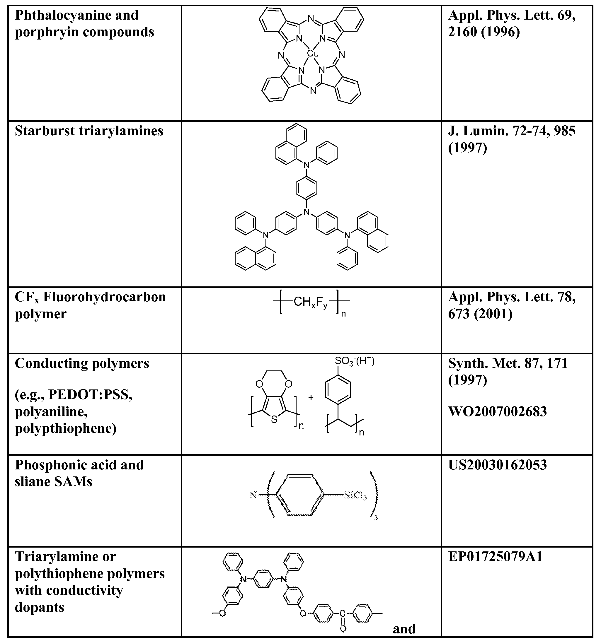
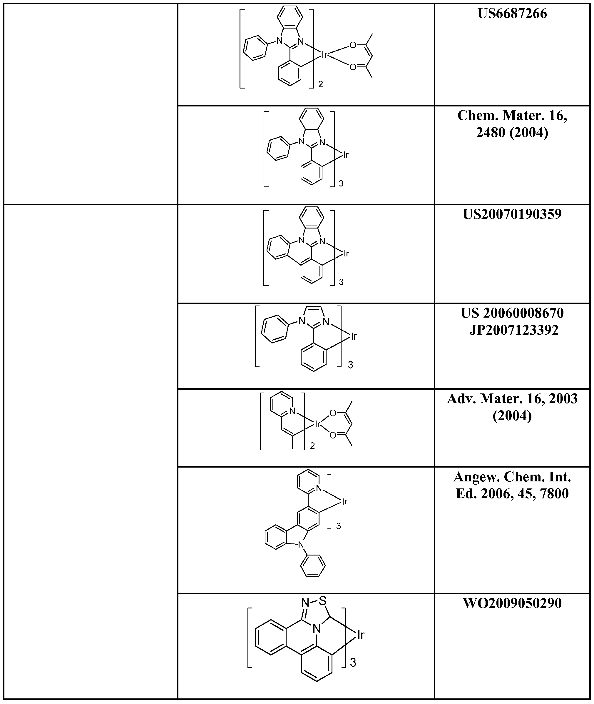
[0064] In addition to and/or in combination with the materials disclosed herein, many hole injection materials, hole transporting materials, host materials, dopant materials, exciton/hole blocking layer materials, electron transporting and electron injecting materials may be used in an OLED. Non- limiting examples of the materials that may be used in an OLED in combination with materials disclosed herein are listed in Table 4 below. Table 4 lists non-limiting classes of materials, non-limiting examples of compounds for each class, and references that disclose the materials.
TABLE 4.


Green dopants


Claims
1. A method of making an organic light emitting device comprising:
providing a substrate;
depositing a translucent low-index material onto a surface over the substrate, wherein the deposition is terminated before the low-index material forms a continuous layer; and
depositing an organic material onto the low-index material, wherein the low-index material has a lower refractive index than the organic material.
2. The method of claim 1, wherein the low-index material is deposited by vapor deposition.
3. The method of claim 1, wherein the deposition of the low-index material forms a discontinuous layer comprising a plurality of discrete elements that are physically isolated from each other, and wherein the deposition of the organic material forms an organic layer.
4. The method of claim 3, wherein the discrete elements are islands.
5. The method of claim 3, wherein the discrete elements have a size in the range of 0.01 - 500 nm.
6. The method of claim 3, wherein the spacing between the discrete elements is less than 500 nm.
7. The method of claim 3, wherein the discontinuous layer is thinner than the organic layer.
8. The method of claim 1 , wherein the low-index material has a refractive index of 1.8 or less.
9. The method of claim 8, wherein the low-index material is an inorganic alkali metal salt.
10. The method of claim 1, wherein the low-index material is deposited to a thickness of 50 A or less.
11. The method of claim 10, wherein the low-index material is deposited to a thickness of 20 A or less.
12. The method of claim 1, wherein the organic material is a charge transport material.
13. The method of claim 1, wherein the organic material is a charge injection material.
14. The method of claim 1, wherein the surface is the surface of the substrate.
15. The method of claim 1, wherein the surface is the surface of another functional organic layer in the device.
16. The method of claim 1, further comprising repeating the steps of depositing the translucent low-index material and depositing the organic material one or more times in an alternating fashion.
17. The method of claim 1, wherein the organic material produces at least 10% greater current as compared to copper phthalocyanine according to a testing protocol using a 2.0 mm2 area square testing device of 2 mm on each side, the testing device consisting of:
a 1200 A thick layer of indium-tin oxide as the testing device anode;
a 100 A thick layer of the test material on the indium-tin oxide anode;
a 300 A thick NPD layer on the test material layer;
a 300 A CBP:Ir(ppy)3 (6%) layer as an emissive layer on the NPD layer;
a 100 A thick BAlq layer on the emissive layer;
a 400 A thick Alq3 layer on the BAlq layer;
a LiF (10 A)/A1 (1000 A) layer on the Alq3 layer as the testing device cathode; wherein the testing protocol is performed by applying a constant 6V to the testing device and measuring the current flow.
18. An organic light emitting device comprising:
a substrate;
a first electrode disposed over the substrate;
a second electrode disposed over the first electrode;
a discontinuous layer disposed between the first and second electrodes, the discontinuous layer comprising a translucent low-index material; and
an organic layer disposed on and in physical contact with the discontinuous layer, the organic layer comprising an organic material;
wherein the low-index material has a lower refractive index than the organic material in the organic layer.
19. The device of claim 18, wherein the discontinuous layer comprises a plurality of discrete elements that are physically isolated from each other.
20. The device of claim 18, wherein the discrete elements have a stochastic pattern.
21. The device of claim 18, wherein the discontinuous layer is thinner than the organic layer.
22. The device of claim 18, wherein the organic layer is a charge transport layer.
23. The device of claim 18, wherein the organic layer is a charge injection layer.
24. The device of claim 18, wherein the discontinuous layer is disposed on and in physical contact with the first electrode.
25. The device of claim 18, wherein the discontinuous layer is disposed on and in physical contact with another functional organic layer in the device.
26. The device of claim 18, wherein the organic layer is a first organic layer, and the discontinuous layer is a first discontinuous layer, and wherein the device further comprises: a second discontinuous layer disposed on the first organic layer, the second discontinuous layer comprising the low-index material; and
a second organic layer disposed on and in physical contact with the second discontinuous layer, the second organic layer comprising an organic material that is the same or different from the organic material used in the first organic layer.
Applications Claiming Priority (2)
| Application Number | Priority Date | Filing Date | Title |
|---|---|---|---|
| US26308109P | 2009-11-20 | 2009-11-20 | |
| US61/263,081 | 2009-11-20 |
Publications (2)
| Publication Number | Publication Date |
|---|---|
| WO2011062857A2 true WO2011062857A2 (en) | 2011-05-26 |
| WO2011062857A3 WO2011062857A3 (en) | 2011-09-29 |
Family
ID=43558310
Family Applications (1)
| Application Number | Title | Priority Date | Filing Date |
|---|---|---|---|
| PCT/US2010/056664 WO2011062857A2 (en) | 2009-11-20 | 2010-11-15 | Oleds with low-index islands to enhance outcoupling of light |
Country Status (1)
| Country | Link |
|---|---|
| WO (1) | WO2011062857A2 (en) |
Cited By (6)
| Publication number | Priority date | Publication date | Assignee | Title |
|---|---|---|---|---|
| CN105118918A (en) * | 2015-07-21 | 2015-12-02 | 苏州大学 | Preparation method of organic-inorganic hybrid charge injection layer |
| US9461262B2 (en) | 2012-03-16 | 2016-10-04 | Cambridge Display Technology Limited | Optoelectronic device |
| US9671529B2 (en) | 2012-08-01 | 2017-06-06 | Ferro Corporation | Light influencing nano layer |
| CN113948660A (en) * | 2021-10-14 | 2022-01-18 | 武汉天马微电子有限公司 | Display panel, manufacturing method thereof and display device |
| WO2022015074A1 (en) * | 2020-07-15 | 2022-01-20 | 경희대학교산학협력단 | Organic light-emitting device including nano-island structures for obtaining color stability and method for manufacturing same |
| KR20220009350A (en) * | 2020-07-15 | 2022-01-24 | 경희대학교 산학협력단 | Organic light emitting device including nano-island structures for improve color stability and manufacturing method thereof |
Citations (17)
| Publication number | Priority date | Publication date | Assignee | Title |
|---|---|---|---|---|
| US4769292A (en) | 1987-03-02 | 1988-09-06 | Eastman Kodak Company | Electroluminescent device with modified thin film luminescent zone |
| US5247190A (en) | 1989-04-20 | 1993-09-21 | Cambridge Research And Innovation Limited | Electroluminescent devices |
| US5703436A (en) | 1994-12-13 | 1997-12-30 | The Trustees Of Princeton University | Transparent contacts for organic devices |
| US5707745A (en) | 1994-12-13 | 1998-01-13 | The Trustees Of Princeton University | Multicolor organic light emitting devices |
| US5834893A (en) | 1996-12-23 | 1998-11-10 | The Trustees Of Princeton University | High efficiency organic light emitting devices with light directing structures |
| US5844363A (en) | 1997-01-23 | 1998-12-01 | The Trustees Of Princeton Univ. | Vacuum deposited, non-polymeric flexible organic light emitting devices |
| US6013982A (en) | 1996-12-23 | 2000-01-11 | The Trustees Of Princeton University | Multicolor display devices |
| US6087196A (en) | 1998-01-30 | 2000-07-11 | The Trustees Of Princeton University | Fabrication of organic semiconductor devices using ink jet printing |
| US6091195A (en) | 1997-02-03 | 2000-07-18 | The Trustees Of Princeton University | Displays having mesa pixel configuration |
| US6097147A (en) | 1998-09-14 | 2000-08-01 | The Trustees Of Princeton University | Structure for high efficiency electroluminescent device |
| US6294398B1 (en) | 1999-11-23 | 2001-09-25 | The Trustees Of Princeton University | Method for patterning devices |
| US6303238B1 (en) | 1997-12-01 | 2001-10-16 | The Trustees Of Princeton University | OLEDs doped with phosphorescent compounds |
| US6337102B1 (en) | 1997-11-17 | 2002-01-08 | The Trustees Of Princeton University | Low pressure vapor phase deposition of organic thin films |
| US20030230980A1 (en) | 2002-06-18 | 2003-12-18 | Forrest Stephen R | Very low voltage, high efficiency phosphorescent oled in a p-i-n structure |
| US20040174116A1 (en) | 2001-08-20 | 2004-09-09 | Lu Min-Hao Michael | Transparent electrodes |
| US7012363B2 (en) | 2002-01-10 | 2006-03-14 | Universal Display Corporation | OLEDs having increased external electroluminescence quantum efficiencies |
| US7279704B2 (en) | 2004-05-18 | 2007-10-09 | The University Of Southern California | Complexes with tridentate ligands |
Family Cites Families (3)
| Publication number | Priority date | Publication date | Assignee | Title |
|---|---|---|---|---|
| JP4564773B2 (en) * | 2004-04-07 | 2010-10-20 | 株式会社 日立ディスプレイズ | LIGHT EMITTING ELEMENT AND DISPLAY DEVICE THEREOF |
| US20090015142A1 (en) * | 2007-07-13 | 2009-01-15 | 3M Innovative Properties Company | Light extraction film for organic light emitting diode display devices |
| KR101135292B1 (en) * | 2007-09-07 | 2012-04-12 | 연세대학교 산학협력단 | Device having a multilayered structure and method of fabricating thereof |
-
2010
- 2010-11-15 WO PCT/US2010/056664 patent/WO2011062857A2/en active Application Filing
Patent Citations (18)
| Publication number | Priority date | Publication date | Assignee | Title |
|---|---|---|---|---|
| US4769292A (en) | 1987-03-02 | 1988-09-06 | Eastman Kodak Company | Electroluminescent device with modified thin film luminescent zone |
| US5247190A (en) | 1989-04-20 | 1993-09-21 | Cambridge Research And Innovation Limited | Electroluminescent devices |
| US5703436A (en) | 1994-12-13 | 1997-12-30 | The Trustees Of Princeton University | Transparent contacts for organic devices |
| US5707745A (en) | 1994-12-13 | 1998-01-13 | The Trustees Of Princeton University | Multicolor organic light emitting devices |
| US5834893A (en) | 1996-12-23 | 1998-11-10 | The Trustees Of Princeton University | High efficiency organic light emitting devices with light directing structures |
| US6013982A (en) | 1996-12-23 | 2000-01-11 | The Trustees Of Princeton University | Multicolor display devices |
| US5844363A (en) | 1997-01-23 | 1998-12-01 | The Trustees Of Princeton Univ. | Vacuum deposited, non-polymeric flexible organic light emitting devices |
| US6091195A (en) | 1997-02-03 | 2000-07-18 | The Trustees Of Princeton University | Displays having mesa pixel configuration |
| US6337102B1 (en) | 1997-11-17 | 2002-01-08 | The Trustees Of Princeton University | Low pressure vapor phase deposition of organic thin films |
| US6303238B1 (en) | 1997-12-01 | 2001-10-16 | The Trustees Of Princeton University | OLEDs doped with phosphorescent compounds |
| US6087196A (en) | 1998-01-30 | 2000-07-11 | The Trustees Of Princeton University | Fabrication of organic semiconductor devices using ink jet printing |
| US6097147A (en) | 1998-09-14 | 2000-08-01 | The Trustees Of Princeton University | Structure for high efficiency electroluminescent device |
| US6294398B1 (en) | 1999-11-23 | 2001-09-25 | The Trustees Of Princeton University | Method for patterning devices |
| US6468819B1 (en) | 1999-11-23 | 2002-10-22 | The Trustees Of Princeton University | Method for patterning organic thin film devices using a die |
| US20040174116A1 (en) | 2001-08-20 | 2004-09-09 | Lu Min-Hao Michael | Transparent electrodes |
| US7012363B2 (en) | 2002-01-10 | 2006-03-14 | Universal Display Corporation | OLEDs having increased external electroluminescence quantum efficiencies |
| US20030230980A1 (en) | 2002-06-18 | 2003-12-18 | Forrest Stephen R | Very low voltage, high efficiency phosphorescent oled in a p-i-n structure |
| US7279704B2 (en) | 2004-05-18 | 2007-10-09 | The University Of Southern California | Complexes with tridentate ligands |
Non-Patent Citations (6)
| Title |
|---|
| BALDO ET AL.: "Highly Efficient Phosphorescent Emission from Organic Electroluminescent Devices", NATURE, vol. 395, 1998, pages 151 - 154, XP001002103, DOI: doi:10.1038/25954 |
| BALDO ET AL.: "Very high-efficiency green organic light-emitting devices based on electrophosphorescence", APPL. PHYS. LETT., vol. 75, no. 3, 1999, pages 4 - 6, XP012023409, DOI: doi:10.1063/1.124258 |
| KULKARNI, A. ET AL., CHEM. MATER., vol. 16, 2004, pages 4556 - 4573 |
| NAKA, S., APPLIED PHYSICS LETTERS, vol. 76, no. 2, 2000, pages 197 - 199 |
| STROHRIEGL, P. ET AL., ADV. MATER., vol. 14, no. 20, 2002, pages 1439 - 1452 |
| YASUDA, T. ET AL., JPN. J. APPL. PHYS., vol. 41, no. 9, 2002, pages 5626 - 5629 |
Cited By (9)
| Publication number | Priority date | Publication date | Assignee | Title |
|---|---|---|---|---|
| US9461262B2 (en) | 2012-03-16 | 2016-10-04 | Cambridge Display Technology Limited | Optoelectronic device |
| US9671529B2 (en) | 2012-08-01 | 2017-06-06 | Ferro Corporation | Light influencing nano layer |
| CN105118918A (en) * | 2015-07-21 | 2015-12-02 | 苏州大学 | Preparation method of organic-inorganic hybrid charge injection layer |
| CN105118918B (en) * | 2015-07-21 | 2017-06-20 | 苏州大学 | A kind of preparation method of organic inorganic hybridization electric charge injection layer |
| WO2022015074A1 (en) * | 2020-07-15 | 2022-01-20 | 경희대학교산학협력단 | Organic light-emitting device including nano-island structures for obtaining color stability and method for manufacturing same |
| KR20220009350A (en) * | 2020-07-15 | 2022-01-24 | 경희대학교 산학협력단 | Organic light emitting device including nano-island structures for improve color stability and manufacturing method thereof |
| KR102623188B1 (en) | 2020-07-15 | 2024-01-11 | 경희대학교 산학협력단 | Organic light emitting device including nano-island structures for improve color stability and manufacturing method thereof |
| CN113948660A (en) * | 2021-10-14 | 2022-01-18 | 武汉天马微电子有限公司 | Display panel, manufacturing method thereof and display device |
| CN113948660B (en) * | 2021-10-14 | 2024-03-01 | 武汉天马微电子有限公司 | Display panel, manufacturing method thereof and display device |
Also Published As
| Publication number | Publication date |
|---|---|
| WO2011062857A3 (en) | 2011-09-29 |
Similar Documents
| Publication | Publication Date | Title |
|---|---|---|
| US20220045294A1 (en) | Three stack hybrid white oled for enhanced efficiency and lifetime | |
| KR102529160B1 (en) | Reducing oled device efficiency at low luminance | |
| US11785804B2 (en) | One way transparent display | |
| US10510973B2 (en) | Color-stable organic light emitting diode stack | |
| JP5886945B2 (en) | OLED with multi-component light emitting layer | |
| US8476822B2 (en) | Saturated color organic light emitting devices | |
| US20150200233A1 (en) | Method of forming bus line designs for large-area oled lighting | |
| US20200083471A1 (en) | Novel oled device structures | |
| US8080937B2 (en) | OLED having a charge transport enhancement layer | |
| WO2010045327A2 (en) | Emissive layer patterning for oled | |
| WO2010028262A9 (en) | White phosphorescent organic light emitting devices | |
| US11217762B2 (en) | Surface-plasmon-pumped light emitting devices | |
| WO2008033194A2 (en) | Organic light emitting device having a microcavity | |
| WO2011062857A2 (en) | Oleds with low-index islands to enhance outcoupling of light | |
| US9640781B2 (en) | Devices to increase OLED output coupling efficiency with a high refractive index substrate | |
| US20170104172A1 (en) | Organic Light Emitting Diode Having a Mixed Blocking Layer | |
| US10038167B2 (en) | Thick-ETL OLEDs with sub-ITO grids with improved outcoupling | |
| KR20220052294A (en) | Energy levels and device structures for plasmonic oleds | |
| KR102077345B1 (en) | Oled fabrication using laser transfer | |
| US20220199932A1 (en) | Optoelectronic device including morphological stabilizing layer | |
| US20230092459A1 (en) | Purcell-Effect-Enhanced Organic Light Emitting Diodes with Sub-Electrode Microlens Array |
Legal Events
| Date | Code | Title | Description |
|---|---|---|---|
| 121 | Ep: the epo has been informed by wipo that ep was designated in this application |
Ref document number: 10782120 Country of ref document: EP Kind code of ref document: A1 |
|
| NENP | Non-entry into the national phase |
Ref country code: DE |
|
| 122 | Ep: pct application non-entry in european phase |
Ref document number: 10782120 Country of ref document: EP Kind code of ref document: A2 |