WO2011141109A1 - Organic electroluminescent devices - Google Patents
Organic electroluminescent devices Download PDFInfo
- Publication number
- WO2011141109A1 WO2011141109A1 PCT/EP2011/001870 EP2011001870W WO2011141109A1 WO 2011141109 A1 WO2011141109 A1 WO 2011141109A1 EP 2011001870 W EP2011001870 W EP 2011001870W WO 2011141109 A1 WO2011141109 A1 WO 2011141109A1
- Authority
- WO
- WIPO (PCT)
- Prior art keywords
- conducting
- organic electroluminescent
- electroluminescent device
- electron
- hole
- Prior art date
Links
Classifications
-
- H—ELECTRICITY
- H10—SEMICONDUCTOR DEVICES; ELECTRIC SOLID-STATE DEVICES NOT OTHERWISE PROVIDED FOR
- H10K—ORGANIC ELECTRIC SOLID-STATE DEVICES
- H10K50/00—Organic light-emitting devices
- H10K50/10—OLEDs or polymer light-emitting diodes [PLED]
- H10K50/11—OLEDs or polymer light-emitting diodes [PLED] characterised by the electroluminescent [EL] layers
-
- H—ELECTRICITY
- H10—SEMICONDUCTOR DEVICES; ELECTRIC SOLID-STATE DEVICES NOT OTHERWISE PROVIDED FOR
- H10K—ORGANIC ELECTRIC SOLID-STATE DEVICES
- H10K30/00—Organic devices sensitive to infrared radiation, light, electromagnetic radiation of shorter wavelength or corpuscular radiation
- H10K30/80—Constructional details
- H10K30/865—Intermediate layers comprising a mixture of materials of the adjoining active layers
-
- H—ELECTRICITY
- H10—SEMICONDUCTOR DEVICES; ELECTRIC SOLID-STATE DEVICES NOT OTHERWISE PROVIDED FOR
- H10K—ORGANIC ELECTRIC SOLID-STATE DEVICES
- H10K50/00—Organic light-emitting devices
- H10K50/10—OLEDs or polymer light-emitting diodes [PLED]
- H10K50/11—OLEDs or polymer light-emitting diodes [PLED] characterised by the electroluminescent [EL] layers
- H10K50/125—OLEDs or polymer light-emitting diodes [PLED] characterised by the electroluminescent [EL] layers specially adapted for multicolour light emission, e.g. for emitting white light
-
- H—ELECTRICITY
- H10—SEMICONDUCTOR DEVICES; ELECTRIC SOLID-STATE DEVICES NOT OTHERWISE PROVIDED FOR
- H10K—ORGANIC ELECTRIC SOLID-STATE DEVICES
- H10K85/00—Organic materials used in the body or electrodes of devices covered by this subclass
- H10K85/30—Coordination compounds
- H10K85/341—Transition metal complexes, e.g. Ru(II)polypyridine complexes
- H10K85/342—Transition metal complexes, e.g. Ru(II)polypyridine complexes comprising iridium
-
- H—ELECTRICITY
- H10—SEMICONDUCTOR DEVICES; ELECTRIC SOLID-STATE DEVICES NOT OTHERWISE PROVIDED FOR
- H10K—ORGANIC ELECTRIC SOLID-STATE DEVICES
- H10K85/00—Organic materials used in the body or electrodes of devices covered by this subclass
- H10K85/30—Coordination compounds
- H10K85/341—Transition metal complexes, e.g. Ru(II)polypyridine complexes
- H10K85/346—Transition metal complexes, e.g. Ru(II)polypyridine complexes comprising platinum
-
- H—ELECTRICITY
- H10—SEMICONDUCTOR DEVICES; ELECTRIC SOLID-STATE DEVICES NOT OTHERWISE PROVIDED FOR
- H10K—ORGANIC ELECTRIC SOLID-STATE DEVICES
- H10K85/00—Organic materials used in the body or electrodes of devices covered by this subclass
- H10K85/60—Organic compounds having low molecular weight
- H10K85/631—Amine compounds having at least two aryl rest on at least one amine-nitrogen atom, e.g. triphenylamine
-
- H—ELECTRICITY
- H10—SEMICONDUCTOR DEVICES; ELECTRIC SOLID-STATE DEVICES NOT OTHERWISE PROVIDED FOR
- H10K—ORGANIC ELECTRIC SOLID-STATE DEVICES
- H10K85/00—Organic materials used in the body or electrodes of devices covered by this subclass
- H10K85/60—Organic compounds having low molecular weight
- H10K85/649—Aromatic compounds comprising a hetero atom
- H10K85/654—Aromatic compounds comprising a hetero atom comprising only nitrogen as heteroatom
-
- H—ELECTRICITY
- H10—SEMICONDUCTOR DEVICES; ELECTRIC SOLID-STATE DEVICES NOT OTHERWISE PROVIDED FOR
- H10K—ORGANIC ELECTRIC SOLID-STATE DEVICES
- H10K2101/00—Properties of the organic materials covered by group H10K85/00
- H10K2101/10—Triplet emission
-
- H—ELECTRICITY
- H10—SEMICONDUCTOR DEVICES; ELECTRIC SOLID-STATE DEVICES NOT OTHERWISE PROVIDED FOR
- H10K—ORGANIC ELECTRIC SOLID-STATE DEVICES
- H10K2101/00—Properties of the organic materials covered by group H10K85/00
- H10K2101/27—Combination of fluorescent and phosphorescent emission
Definitions
- the present invention relates to white emitting organic electroluminescent devices with two emitting layers, which contain an emitting layer with a phosphorescent dopant and an emitting layer with a fluorescent dopant.
- OLEDs organic electroluminescent devices
- OLEDs organic electroluminescent devices
- WO 98/27136 A development in the field of organic electroluminescent devices are white-emitting OLEDs. These can be used either for monochrome white displays or with color filters for full-color displays. Furthermore, they are suitable for lighting applications.
- White-emitting organic electroluminescent devices based on low molecular weight compounds generally have at least two emission layers. In this case, electroluminescent devices with exactly two emission layers are used, in particular for passive matrix applications, frequently only using fluorescent emitters according to the prior art. Most of the electroluminescent devices have at least three emission layers, which are blue, green and orange or red
- the phosphorescent emitters show significant advantages due to the higher achievable efficiency.
- the general structure of such a white-emitting OLED having at least one phosphorescent layer is described, for example, in WO 2005/011013. Because of the higher achievable efficiency, a white-emitting OLED containing only phosphorescent emitter layers would be desirable.
- blue-phosphorescent emitters generally do not yet meet the usual requirements, in particular with regard to the service life, in most of the prior art
- Hybrid OLEDs are used, ie a fluorescent blue emitter layer combined with phosphorescent orange or red and green emitter layers (in the case of three-color white) or a fluorescent ornamental blue emitter layer combined with a phosphorescent yellow to orange emitter layer (in the case of two-color white).
- a fundamental problem of such hybrid OLEDs is that common matrix and emitter materials used in the blue-fluorescent emitter layer have too low a triplet level for phosphorescent dopants, which can lead to triplet excitons via the blue emitter layer to be deleted. This leads to a low efficiency of the OLED. In order to obtain maximum efficiency from a white hybrid OLED, care must be taken to prevent this quenching of triplet excitons.
- One prior art approach is to prevent direct contact between the fluorescent emitter layer and the phosphorescent emitter layer by introducing a non-luminous interlayer. This intermediate layer usually consists of a mixture of two materials, one having rather hole-conducting and the other more electron-conducting properties.
- US 2006/130883 discloses an intermediate layer between the fluorescent and phosphorescent emitter layers in a white-emitting OLED, wherein preferably the same material is used in the intermediate layer and in the two adjacent emitter layers.
- an intermediate layer between the fluorescent and the phosphorescent emitter layer in a white emitting OLED discloses, wherein the intermediate layer preferably contains a hole transport and an electron transport material.
- US 2007/0099026 discloses white-emitting organic electroluminescent devices, wherein the green, yellow or red-emitting layer comprises a phosphorescent emitter and a
- the interlayer should not significantly affect the charge balance. It must be capable of transporting holes and electrons to a sufficient and balanced extent so that the emitter layers on both sides of the interlayer are properly supplied with both types of charge carriers. Only then can a white color location be realized. This severely restricts the candidate materials for HOMO and LUMO energies.
- the interlayer must not substantially reduce the service life of the OLED.
- the technical problem underlying the present invention is therefore to provide a device architecture for a hybrid OLED with exactly two emitting layers, which makes it possible to easily and reproducibly set a desired white color location while at the same time achieving high efficiency with a long service life combine.
- an OLED having exactly two emitting layers in which a non-emitting intermediate layer is inserted between the phosphorescent emitter layer and the fluorescent emitter layer and in which at least one of the emitting layers contains a dopant doped in a mixture of at least two matrix materials, Achieved a very good efficiency and the operating life compared to an OLED, which does not have such a device structure, is significantly improved. Furthermore, the color locus can be adjusted very well with such a device structure.
- the invention thus relates to an organic electroluminescent device, comprising anode, cathode and exactly two emitting layers, of which one emitting layer is a phosphorescent Contains compound and the other emitting layer contains a fluorescent compound, characterized in that between the two emitting layers at least one intermediate layer is present and further that at least one of the two emitting compounds is doped in a mixture of at least two materials.
- the longer wavelength emitting layer contains the phosphorescent compound
- the shorter wavelength emitting layer contains the fluorescent compound.
- doping compounds is doped, it is matrix materials.
- a matrix material is a material that in one
- Emission layer can be used to doped therein the emissive material in typically a volume concentration of ⁇ 25%, but itself, in contrast to the doped emitter material, does not contribute significantly to the light emission. Which materials in an emitter layer contribute significantly to the light emission and which do not, and which materials are thus to be regarded as emitter and which as matrix materials can be detected by comparing the electroluminescence spectrum of the OLED in which the emitter layer is present with photoluminescence spectra of the individual materials become. The photoluminescence spectrum of the individual materials in solution is measured in a concentration of 1.5 mg in 250 ml of solvent, the measurement being carried out at room temperature and any solvent is suitable in which the substance dissolves in said concentration.
- Particularly suitable solvents are usually toluene, but also dichloromethane.
- exactly one intermediate layer is present between the two emitting layers.
- This is preferably a non-emitting intermediate layer, that is, this layer shows no emission during operation of the OLED. This can in turn be detected by comparing the electroluminescence spectrum of the OLED with photoluminescence spectra of the materials from the intermediate layer.
- a preferred embodiment of the invention is a white-emitting organic electroluminescent device.
- CIE color coordinates in the range of 0.25 ⁇ CIE x ⁇ 0.45 and 0.25 ⁇ CIE y ⁇ 0.48, preferably 0.28 ⁇ CIE x ⁇ 0.38 and 0.29 ⁇ CIE y ⁇ 0.38 and particularly preferably 0.30 ⁇ CIE x ⁇ 0.35 and 0.31 ⁇ CIE y ⁇ 0.35.
- CIE color coordinates in the range of 0.38 ⁇ x ⁇ 0.47 and 0.38 ⁇ y ⁇ 0.44 and particularly preferably 0.41 ⁇ x ⁇ 0.46 and 0.40 ⁇ y ⁇ 0.43 are also preferred.
- the organic electroluminescent device comprises, as described above, anode, cathode and exactly two emitting layers, which are arranged between the anode and the cathode.
- the organic electroluminescent device does not necessarily have to contain only layers which are composed of organic or metal-organic materials.
- the anode, cathode and / or one or more layers contain inorganic materials or are constructed entirely from inorganic materials.
- the fluorescent emitter layer is a blue emitting layer and the phosphorescent emitter layer is a yellow, orange or red emitting emitter layer.
- the blue emitting layer may be a deep blue or a light blue emitting layer. Particularly preferred is the combination of a light blue emitter layer with an orange emitter layer.
- the yellow, orange or red phosphorescent layer can be arranged on the anode side and the blue fluorescent layer on the cathode side.
- the yellow or orange phosphorescent layer can be arranged on the cathode side and the blue fluorescent layer on the anode side
- the organic electroluminescent device according to the invention has the following
- This structure is shown schematically in FIG. 1, wherein (1) stands for the anode, (2) for the phosphorescent emitter layer, (3) for the intermediate layer, (4) for the fluorescent emitter layer and (5) for the cathode.
- the organic electroluminescent device according to the invention may also contain further layers, which are not shown in FIG. Preferably, therefore, the shorter wavelength emitting, fluorescent emitter layer is arranged on the cathode side.
- the photoluminescence maximum in the range of 540 to 570 nm is understood as meaning a layer whose photoluminescence maximum lies in the range from 570 to 600 nm.
- a red-emitting layer is understood as meaning a layer whose photoluminescence maximum lies in the range from 600 to 750 nm.
- a green-emitting layer is understood as meaning a layer whose photoluminescence maximum lies in the range from 490 to 540 nm.
- a light blue emitting layer is understood as meaning a layer whose photoluminescence maximum lies in the range from 460 to 490 nm
- a deep blue emitting layer is understood as meaning a layer whose photoluminescence maximum lies in the range from 440 to 460 nm.
- the photoluminescence maximum is determined by measuring the photoluminescence spectrum of the layer with a layer thickness of 50 nm, the layer having the same composition as in the organic electroluminescent device, ie containing emitter and matrix.
- a phosphorescent compound in the sense of this invention is a compound which exhibits luminescence at room temperature from an excited state with a higher spin multiplicity, ie a spin state> 1, in particular from one excited triplet state.
- all luminescent transition metal complexes in particular all luminescent iridium, platinum and copper compounds, are to be regarded as phosphorescent compounds.
- a fluorescent compound in the sense of this invention is a compound which exhibits luminescence from an excited singlet state at room temperature.
- all luminescent compounds which are composed only of the elements C, H, N, O, S, F, B and P are to be understood as fluorescent compounds.
- the organic electroluminescent device contains exactly one intermediate layer between the two emitting layers.
- the intermediate layer must have both hole-conducting and electron-conducting properties.
- the intermediate layer can be constructed from a single material which has both hole-conducting properties and also electron-conducting properties. In a preferred embodiment of the invention, however, the intermediate layer contains a mixture of at least one hole-conducting material and at least one electron-conducting material. In a particularly preferred embodiment of the invention, the intermediate layer contains a mixture of exactly one hole-conducting material and exactly one electron-conducting material.
- both the hole-conducting material and the electron-conducting material are preferably materials whose triplet energy is greater than the triplet energy of the emitter of the adjacent phosphorescent emitter layer.
- the triplet energy of the hole-conducting and the electron-conducting material of the intermediate layer is> 2.1 eV, particularly preferably> 2.3 eV.
- the triplet energy E (Ti) of a molecule is defined as the energy difference between the energy of the ground state E (G) of a molecule and the energy of the lowest triplet state E (T) of that molecule, both energies in eV. This size can be determined experimentally or calculated by quantum chemical methods. For the experimental determination one makes the optical transition from the
- This transition is also called phosphorescence, which is typically a
- the apparatus sensitivity to a simple photoluminescence spectrometer can be increased by using a (pulsed) laser for excitation in the absorption maximum and for detection, a spectrometer, which allows a time-delayed detection to z.
- B. temporally hide an also occurring intense fluorescence.
- the triplet energy can not be determined experimentally by the above-mentioned method, an alternative is to use the triplet energy with the aid of a quantum-chemical calculation, eg. Example by means of time-dependent density functional theory (TD-DFT) to determine. This is done via the commercially available software Gaussian 03W (Gaussian Inc.) with the method B3PW91 / 6-31 G (d).
- the basis set LANL2DZ is used for the calculation of transition metal complexes.
- the hole-conducting material used in the intermediate layer preferably has a HOMO (highest occupied molecular orbital) of> -5.4 eV, more preferably> -5.2 eV.
- the electron-conductive material used in the intermediate layer preferably has a LUMO (lowest unoccupied molecular orbital) of ⁇ - 2.4 eV, more preferably ⁇ - 2.6 eV.
- the intermediate layer contains a material which is capable of transporting both electrons and holes.
- This material preferably has a HOMO of> _5.6 eV, more preferably> - 5.4 eV and a LUMO of ⁇ -2.4 eV, particularly preferably ⁇ -2.6 eV.
- the electron-conducting compound in the intermediate layer is preferably between 90:10 and 10:90, more preferably between 80:20 and 20:80, in each case based on the volume.
- the layer thickness of the intermediate layer is preferably between 1 and 20 nm, particularly preferably between 2 and 10 nm, very particularly preferably between 4 and 8 nm.
- the electron-conducting material of the intermediate layer is an aromatic ketone.
- an aromatic ketone is understood as meaning a carbonyl group to which two aryl or heteroaryl groups or aromatic or heteroaromatic ring systems are directly bonded.
- the aromatic ketone is a compound of the following formula (1)
- Ar is the same or different at each occurrence, an aromatic or heteroaromatic ring system having 5 to 60 aromatic ring atoms, which may be substituted in each case with one or more groups R 1 ;
- R 1 is the same or different H, D, F, Cl, Br, I at each occurrence
- R 2 is identical or different at each occurrence, H, D, CN or an aliphatic, aromatic and / or heteroaromatic hydrocarbon radical having 1 to 20 carbon atoms, in which H atoms may be replaced by D or F; two or more adjacent substituents R 2 may also together form a mono- or polycyclic, aliphatic or aromatic ring system.
- An aryl group in the sense of this invention contains at least 6 C atoms;
- a heteroaryl group contains at least 2 C atoms and at least 1 heteroatom, with the proviso that the sum of C atoms and heteroatoms gives at least 5.
- Heteroatoms are preferably selected from N, O and / or S.
- an aryl group or heteroaryl group is either a simple aromatic cycle, ie benzene, or a simple heteroaromatic cycle, for example pyridine, pyrimidine, thiophene, etc., or a condensed Aryl or heteroaryl group, for example naphthalene, anthracene, pyrene, quinoline, isoquinoline, etc., understood.
- An aromatic ring system according to this invention contains
- a heteroaromatic ring system in the sense of this invention contains at least 2 C atoms and at least one heteroatom in the ring system, with the proviso that the sum of C atoms and heteroatoms gives at least 5.
- Heteroatoms are preferably selected from N, O and / or S.
- An aromatic or heteroaromatic ring system in the sense of this invention is to be understood as meaning a system which does not necessarily contain only aryl or heteroaryl groups, but in which also several Aryl or heteroaryl groups by a short, non-aromatic moiety, such as.
- a C, N or O atom or a carbonyl group may be connected.
- systems such as 9,9'-spirobifluorene, 9,9-diarylfluorene, triarylamine, diaryl ether, diarylmethane, stilbene, benzophenone, etc. are also to be considered as aromatic ring systems in the sense of this
- an aromatic or heteroaromatic ring system is understood as meaning systems in which a plurality of aryl or heteroaryl groups are linked together by single bonds, for example biphenyl, terphenyl or bipyridine.
- a d- to C 0 -alkyl group in which individual H atoms or CH 2 groups may be substituted by the abovementioned groups, particularly preferably the radicals methyl, ethyl, n-propyl, i Propyl, n-butyl, i-butyl, s-butyl, t-butyl, 2-methylbutyl, n-pentyl, s -pentyl, t -pentyl, 2-pentyl, neo-pentyl, cyclopentyl, n -hexyl , s-hexyl, t -hexyl, 2-hexyl, 3-hex
- alkenyl group are preferably ethenyl, propenyl, butenyl, pentenyl, cyclopentenyl, hexenyl, cyclohexenyl, heptenyl, cycloheptyl, octenyl and cyclooctenyl understood.
- o-alkynyl are preferably ethynyl, propynyl, butynyl, pentynyl, hexynyl, heptynyl and octynyl understood.
- a C 1 - to C 40 -alkoxy group are particularly preferably understood methoxy, trifluoromethoxy, ethoxy, n-propoxy, i-propoxy, n-butoxy, i-butoxy, s-butoxy, t-butoxy or 2-methylbutoxy.
- aromatic or heteroaromatic ring system having 5-60 aromatic ring atoms, which may be substituted in each case with the abovementioned radicals R and which may be linked via any positions on the aromatic or heteroaromatic, are understood in particular groups which are derived from benzene, Naphthalene, anthracene, phenanthrene, benzanthracene, pyrene, chrysene, perylene, fluoranthene, benzfluoranthene, naphthacene, pentacene, benzopyrene, biphenyl, biphenylene, terphenyl, terphenylene, fluorene, benzofluorene, dibenzofluorene, spirobifluorene, Dihydrophenanthrene, dihydropyrenes, tetrahydropyrenes, cis- or trans-indenofluorene, cis- or trans-monobenzoindenofluoren
- Anthroxazole phenanthroxazole, isoxazole, 1, 2-thiazole, 1, 3-thiazole,
- Suitable compounds according to formula (1) are in particular the ketones disclosed in WO 2004/093207 and WO 20/006680. These are via quote part of the present invention.
- the definition of the compound according to formula (1) shows that it does not only have to contain one carbonyl group but also contain several carbonyl groups.
- the group Ar in compounds according to formula (1) is preferably an aromatic ring system having 6 to 40 aromatic ring atoms, ie it contains no heteroaryl groups. As defined above, the aromatic ring system does not necessarily have to contain only aromatic groups, but two aryl groups can also be substituted by a non-aromatic group. aromatic group, for example, be interrupted by another carbonyl group.
- the group Ar has no more than two condensed rings. It is therefore preferably composed only of phenyl and / or naphthyl groups, particularly preferably only of phenyl groups, but does not contain any larger condensed aromatics, for example anthracene.
- Preferred groups Ar which are bonded to the carbonyl group are phenyl, 2-, 3- or 4-tolyl, 3- or 4-o-xylyl, 2- or 4-m-xylyl, 2-p-xylyl,
- the groups Ar may be substituted by one or more radicals R.
- substituents R 1 When the organic electroluminescent device is applied from solution, straight-chain, branched or cyclic alkyl groups having up to 10 C atoms are also preferred as substituents R 1 .
- the group Ar 1, identical or different at each occurrence is an aromatic ring system having 6 to 24 aromatic ring atoms which may be substituted by one or more radicals R 2 .
- Ar 1 is more preferably identical or different at each occurrence, an aromatic ring system having 6 to 12 aromatic ring atoms.
- benzophenone derivatives which are each substituted at the 3,5,3 ', 5' positions by an aromatic or heteroaromatic ring system having 5 to 30 aromatic ring atoms, which in turn is replaced by one or more radicals R 1 as defined above may be substituted.
- Preferred aromatic ketones are therefore furthermore the compounds of the following formula (2) to (5)
- Z is the same or different every occurrence CR or N; n is the same or different at every occurrence 0 or 1.
- Ar in the formulas (2), (4) and (5) is preferably an aromatic or heteroaromatic ring system having 5 to 30 aromatic ring atoms which does not have condensed aryl groups with more than 10 aromatic ring atoms, preferably no condensed aryl groups at all, and which may be substituted by one or more radicals R 1 .
- Particular preference is given to the groups Ar mentioned above as being preferred. Ebenson particularly preferred are the above mentioned as preferred groups R 1 .
- Examples of suitable compounds according to formulas (1) to (5) which can be used as electron-conducting material in the intermediate layer are the compounds (1) to (59) depicted below.
- the electron-conducting material is a triazine derivative which is substituted by at least one aromatic or heteroaromatic ring system, preferably by at least two aromatic or heteroaromatic ring systems, more preferably by three aromatic or heteroaromatic ring systems.
- Suitable triazine derivatives which can be used as the electron-conductive material are therefore compounds of the following formula (6) or (7),
- Ar 2 is identical or different at each occurrence, a monovalent aromatic or heteroaromatic ring system having 5 to 60 aromatic ring atoms, which may be substituted in each case by one or more radicals R; is a bivalent aromatic or heteroaromatic ring system having 5 to 60 aromatic ring atoms, which may be substituted by one or more radicals R 1 .
- X is the same or different at each occurrence as a bivalent
- m is the same or different at each occurrence 0, 1, 2 or 3;
- o is the same or different 0, 1, 2, 3 or 4 at each occurrence.
- X in formula (14) and (15) is NR 1 or C (R 1 ) 2 .
- Particularly preferred groups Ar 2 are selected from the groups of the following formulas (8a) to (15a),
- X is preferably identical or different selected from C (R 1 ) 2 , N (R 1 ), O and S, particularly preferably C (R 1 ) 2 .
- Preferred compounds of the formula (6) have one or two groups of the above-mentioned formula (8) to (15), in particular a group, and have two or one groups selected from phenyl, 1-naphthyl, 2-naphthyl , ortho-, meta- or para-biphenyl, which may each be substituted by one or more radicals R 1 .
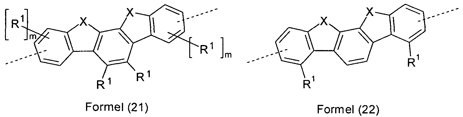
- Preferred groups Ar 3 in compounds of the formula (7) are selected from the groups of the following formulas (16) to (22),
- Particularly preferred groups Ar are selected from the groups of the following formulas (16a) to (22a),
- Formula (21a) Formula (22a) wherein the symbols and indices used have the same meaning as described above.
- X is preferably identical or different selected from C (R 1 ) 2 , N (R 1 ), O and S, particularly preferably C (R 1 ) 2 .
- Examples of suitable triazine derivatives are structures 1 to 150 depicted below.
- the hole-conducting compound in the intermediate layer is preferably an aromatic diamine, triamine or tetramine.
- Preferred aromatic amines are the compounds of the following formulas (23) to (28),
- Ar 4 is identical or different at each occurrence and is a bivalent
- Ar 4 in the compounds of the formulas (23), (24), (25) and (28) is a divalent group and in the compounds of the formula (26) a trivalent group and in the compounds of the formula (27) a tetra - valent group. It is preferred if Ar 4 and Ar 5 contain no condensed aryl or heteroaryl groups having more than 10 aromatic ring atoms.
- Suitable hole-conducting compounds in the intermediate layer are the aromatic amines depicted below.
- hole-conducting compounds which can be used in the intermediate layer are diazasilol and tetraazasilol derivatives, in particular with aromatic substituents, as described, for example, in WO 2010/054729.
- the preferred embodiments are carried out for the emitting layers and for the further layers of the OLED.
- the emitting compound in at least one emitting layer, is doped in a mixture of at least two matrix materials.
- Suitable phosphorescent compounds as used in the phosphorescent emitting layer are, in particular, compounds which emit light, preferably in the visible range, when suitably excited, and moreover preferably at least one atom of atomic number greater than 20, preferably greater than 38 and less than 84 greater 56 and less than 80 included.
- Transition metal compounds in particular compounds which contain copper, molybdenum, tungsten, rhenium, ruthenium, osmium, rhodium, iridium, palladium, platinum, silver, gold or europium, are preferably used as phosphorescence emitters, in particular compounds which contain iridium, platinum or copper.
- Particularly preferred organic electroluminescent devices contain at least one phosphorescent compound
- DCy is the same or different at each occurrence, a cyclic one
- CCy is the same or different at each occurrence a cyclic
- A is the same or different at each occurrence as a mononionic, bidentate chelating ligand, preferably a diketonate ligand.
- ring systems between a plurality of radicals R 1 there may also be a bridge between the groups DCy and CCy. Furthermore, by forming ring systems between several radicals R 1, there may also be a bridge between two or three ligands CCy-DCy or between one or two ligands CCy-DCy and the ligand A, so that it is a polydentates or polypodal
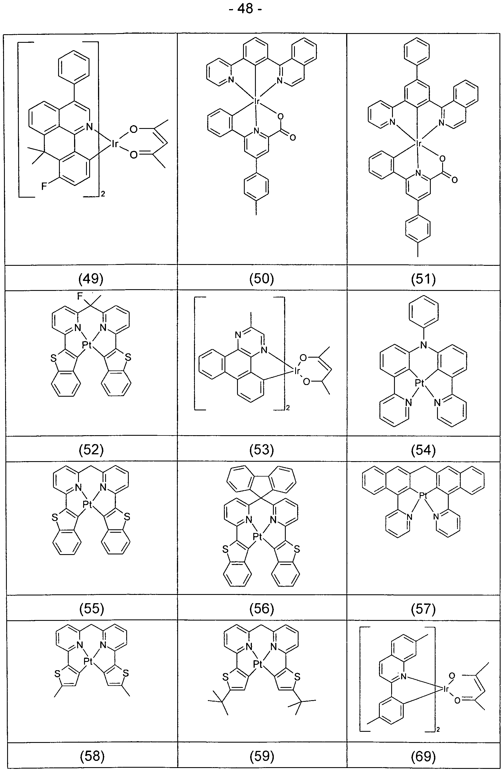
- Examples of the emitters described above can be found in applications WO 2000/70655, WO 2001/41512, WO 2002/02714, WO 2002/15645, EP 1191613, EP 1191612, EP 1191614, WO 2004/081017, WO 2005/033244, WO 2005/042550, WO 2005/113563, WO 2006/008069, WO 2006/061182, WO 2006/081973 and WO 2009/146770.
- all the phosphorescent complexes used in the prior art for phosphorescent OLEDs and as known to those skilled in the art of organic electroluminescence, and the skilled artisan can use other phosphorescent compounds without inventive step.
- the person skilled in the art knows which phosphorescent complexes emit with which emission color. Examples of suitable phosphorescent emitters are listed in the following table.
- matrix material for the phosphorescent compound various materials are used, such as are used according to the prior art as matrix materials for phosphorescent compounds.
- Suitable matrix materials for the phosphorescent emitter are aromatic ketones, in particular selected from compounds of the above depicted formula (1) to (5) or aromatic phosphine oxides or aromatic sulfoxides or sulfones, for. B. according to WO 2004/013080, WO 2004/093207, WO 2006/005627 or WO 2010/006680, triarylamines, z. B. NPB, carbazole derivatives, z. B.
- CBP N, N-Biscarbazolylbiphenyl
- mCBP in WO 2005/039246, US 2005/0069729, JP 2004/288381, EP 1205527 or WO 2008/086851 disclosed carbazole derivatives, indolocarbazole derivatives, z. B. according to WO 2007/063754 or WO 2008/056746, indenocarbazole derivatives, for. B. according to WO 2010/136109 and WO
- Triazine derivatives in particular selected from compounds of the above-depicted formula (6) or (7), z. B. according to WO 2010/015306, WO 2007/063754 or WO 2008/056746, zinc complexes, for. B. according to
- EP 652273 or WO 2009/062578 Diazasilol- or tetraazasilol derivatives, z. B. according to WO 2010/054729, or Diazaphospholderivate, z. B. according to WO 2010/054730.
- a hole-conducting matrix material This is defined as a compound with a HOMO of> -5.6 eV, preferably> -5.3 eV.
- Particularly preferred is an arylamine, in particular an arylamine, as described above by the
- Matrix materials are NPB or N, N, N ', N'-tetrakis (biphenyl) -4,4'-diaminobiphenyl or the other compounds depicted above.
- the matrix material for the phosphorescent compound if it is to a hole-conducting matrix material is the same material which is also used as a hole-conducting material in the intermediate layer.
- the phosphorescent emitter is doped in a mixture of at least two matrix materials, preferably exactly two matrix materials.
- the mixing ratio depends on whether the phosphorescent emitter layer is on the anode side or on the cathode side. If the phosphorescent emitter layer is present on the anode side, the ratio of the hole-conducting matrix material to the electron-conducting matrix material is preferably between 95: 5 and 50:50, particularly preferably between 90:10 and 70:30, in each case based on the volume.
- the hole-conducting compound is defined as a compound having a HOMO of> -5.6 eV, preferably> -5.3 eV. It is then particularly preferred to use an arylamine, in particular an arylamine, as defined above by the formulas (23) to (28).
- the electron-conducting compound is defined as a compound having a LUMO of ⁇ -2.4 eV, preferably ⁇ -2.6 eV. More preferably, it is a triazine derivative as defined above by the formulas (6) or (7), or a corresponding pyrimidine or pyrazine derivative or an aromatic ketone as defined above by the formulas (1) to (5) ) is defined.
- the matrix material for the phosphorescent compound if it is an electron-conducting matrix material, is the same material which is also used as the electron-conducting material in the intermediate layer.
- a mixture of a hole-conducting and an electron-conducting material is used both in the phosphorescent emitter layer and in the intermediate layer.
- the same hole-conducting and the same electron-conducting compounds are particularly preferably used in the phosphorescent emitter layer and in the intermediate layer.
- the phosphorescent emitter layer may be advantageous to use in the phosphorescent emitter layer a mixture of a charge-transporting matrix material and a further matrix material which has neither electron-conducting nor hole-conducting properties.
- the charge-transporting matrix material is a hole-conducting material if the phosphorescent emitter layer is present on the anode side, and an electron-conducting material if the phosphorescent emitter layer is present on the cathode side. This can increase the efficiency and the lifetime of the organic electroluminescent device.
- the fluorescent emitter layer contains a fluorescent dopant, in particular a blue-fluorescent dopant, and at least one matrix material.
- the fluorescent emitter layer particularly preferably contains a fluorescent dopant, in particular a blue-fluorescent dopant, and exactly one matrix material Suitable fluorescent dopants, in particular blue-fluorescent dopants, are for example selected from the group of monostyrylamines, distyrylamines, tristyrylamines, tetrastyrylamines Styrylphosphines, the styryl ether and the arylamine.
- a monostyrylamine is understood as meaning a compound which contains a substituted or unsubstituted styryl group and at least one, preferably aromatic, amine.
- a distyrylamine is understood as meaning a compound which contains two substituted or unsubstituted styryl groups and at least one, preferably aromatic, amine.
- a tristyrylamine is understood as meaning a compound which contains three substituted or unsubstituted styryl groups and at least one, preferably aromatic, amine.
- a tetrastyrylamine is meant a compound containing four substituted or unsubstituted styryl groups and at least one, preferably aromatic, amine.
- the styryl groups are particularly preferably silibene, which may also be further substituted.
- Corresponding phosphines and ethers are defined in analogy to the amines.
- An arylamine or an aromatic amine in the context of this invention is understood as meaning a compound which contains three substituted or unsubstituted aromatic or heteroaromatic ring systems bonded directly to the nitrogen. At least one of these aromatic or heteroaromatic ring systems is preferably a condensed ring system, particularly preferably having at least 14 aromatic ring atoms.
- Preferred examples of these are aromatic anthracene amines, aromatic pyrenamines, aromatic pyrenediamines, aromatic chrysenamines or aromatic chrysendiamines.
- aromatic anthracene amine a compound in which a diarylamino group is bonded directly to an anthracene group, preferably in the 9-position or in the 2-position.
- Aromatic pyrenamines, pyrenediamines, chrysenamines and chrysenediamines are defined analogously thereto, the diarylamino groups on the pyrene preferably being bonded in the 1-position or in the 1, 6-position.
- dopants are selected from indenofluorenamines or diamines, for example according to WO 2006/108497 or WO 2006/122630, benzoindenofluorenamines or -diamines, for example according to WO 2008/006449, and dibenzoindeno-fluorenamines or -diamines, for example according to WO 2007 / 140,847th
- dopants from the class of styrylamines are substituted or unsubstituted tristilbenamines or the dopants described in WO
- Suitable host materials (matrix materials) for the fluorescent dopants are selected, for example, from the classes of the oligoarylenes (for example 2,2 ', 7,7'-tetraphenylspirobifluorene according to EP 676461 or dinaphthylanthracene), in particular the oligoarylenes containing condensed aromatic groups, in particular anthracenes, the oligoarylenevinylenes (eg DPVBi or spiro-DPVBi according to EP 676461), the polypodal metal complexes (eg according to WO 2004/081017), the hole-conducting compounds (eg according to WO 2004/058911), the electron-conducting compounds, in particular ketones, phosphine oxides, sulfoxides, etc. (for example according to WO 2005/084081 and WO 2005/084082), the atropisomers (for example according to WO
- Particularly preferred host materials are selected from the classes of oligoarylenes containing naphthalene, anthracene, Benzanthracen, in particular Benz [a] anthracene, Benzophenanthren, in particular Benz [c] phenanthren, and / or pyrene or atropisomers of these compounds.
- Very particularly preferred matrix materials for the fluorescent emitter are anthracene derivatives.
- an oligoarylene is to be understood as meaning a compound in which at least three aryl or arylene groups are bonded to one another.
- the fluorescent emitter layer contains a mixture of two matrix materials
- one of the two matrix materials is preferably selected from the group of the oligoarylenes, as described above, in particular the anthracene derivatives.
- the second matrix material of the mixture is then preferably a hole-conducting material which is defined by a HOMO of> -5.6 eV, preferably> -5.3 eV. It is then particularly preferred to use an arylamine, in particular an arylamine, as defined above by the formulas (23) to (28).
- suitable hole-conducting matrix materials are NPB or N, N, N ', N'-tetrakis (biphenyl) -4,4'-diaminobiphenyl.
- the organic electroluminescent device may also contain further layers, which are not shown in FIG. These are, for example, selected from in each case one or more hole injection layers, hole transport layers, Hole blocking layers, electron transport layers, electron injection layers, electron blocking layers, exciton blocking layers, charge generation layers (charge generation layers) and / or organic or inorganic p / n junctions.
- the layers, in particular the charge transport layers may also be doped. The doping of the layers may be advantageous for improved charge transport. It should be noted, however, that not necessarily each of these layers must be present and the choice of layers always depends on the compounds used.
- metals having a low work function metal alloys or multilayer structures of different metals are preferred, such as alkaline earth metals, alkali metals, main group metals or lanthanides (eg Ca, Ba, Mg, Al, In, Mg, Yb, Sm, Etc.).
- alkaline earth metals alkali metals
- main group metals or lanthanides eg Ca, Ba, Mg, Al, In, Mg, Yb, Sm, Etc.
- further metals which have a relatively high work function such as, for example, B. Ag, which then usually combinations of metals, such as Mg / Ag, Ca / Ag or Ba / Ag are used.
- metal alloys in particular alloys of an alkali metal or alkaline earth metal and silver, particularly preferably an alloy of Mg and Ag. It may also be preferred to introduce between a metallic cathode and the organic semiconductor a thin intermediate layer of a material with a high dielectric constant.
- alkali metal or alkaline earth metal fluorides but also the corresponding oxides or carbonates in question (eg., LiF, Li 2 O, CsF, CS 2 CO 3, BaF 2 , MgO, NaF, etc.), as well as organic alkali metal complexes, eg. B. Liq (lithium quinolinate).
- the layer thickness of this layer is preferably between 0.5 and 5 nm.
- the anode of the electroluminescent device materials having a high work function are preferred.
- the anode a work function greater than 4.5 eV vs. Vacuum up.
- metals with a high redox potential such as Ag, Pt or Au, are suitable for this purpose.
- metal / metal oxide electrodes for example Al / Ni / NiO x , Al / PtOx
- At least one of the electrodes must be transparent or partially transparent in order to enable the extraction of light.
- Preferred anode materials here are conductive mixed metal oxides. Particularly preferred are indium tin oxide (ITO) or indium zinc oxide (IZO).
- the device is structured accordingly (depending on the application), contacted and finally hermetically sealed because the life of such devices drastically shortened in the presence of water and / or air.
- all other materials which are used in organic electroluminescent devices according to the prior art can also be used in combination with the intermediate layers according to the invention.
- Suitable charge transport materials, as used in Lochinjetechnische transport layer or in the electron transport layer of the organic electroluminescent device according to the invention are, for example, the compounds disclosed in Y. Shirota et al., Chem. Rev. 2007, 107 (4), 953-1010 or other materials as known from the prior art Technique can be used in these layers.
- Examples of preferred hole transport materials which can be used in a hole transport or hole injection layer in the electroluminescent device according to the invention are indenofluorenamines and derivatives (for example according to WO 2006/122630 or WO
- Suitable hole transport or hole injection materials are, for example, the materials listed in the following table.
- materials for the electron transport layer it is possible to use all materials as used in the prior art as electron transport materials in the electron transport layer.
- Particularly suitable are aluminum complexes, for example Alq 3 , zirconium complexes, for example Zrq 4 , benzimidazole derivatives, triazine derivatives, for example compounds of the abovementioned formulas (6) or (7), or aromatic ketones, for example compounds of the abovementioned formulas (1) to ( 5).
- Suitable materials are, for example, the materials listed in the following table. Further suitable materials are derivatives of the compounds depicted above, as disclosed in JP 2000/053957, WO 2003/060956, WO 2004/028217 and WO 2004/080975.
- the electron transport layer is doped. Suitable dopants are alkali metals or alkali metal compounds, such as Liq (lithium quinolinate).
- the electron transport layer is doped in particular when the electron transport material is a benzimidazole derivative or a triazine derivative. The preferred dopant is then Liq.
- an organic electroluminescent device characterized in that one or more layers are coated with a sublimation process.
- the materials in vacuum sublimation systems become smaller at an initial pressure
- an organic electroluminescent device characterized in that one or more layers are coated with the OVPD (Organic Vapor Phase Deposition) method or with the aid of a carrier gas sublimation.
- the materials are applied at a pressure between 10 "applied 5 mbar and 1 bar.
- OVJP organic vapor jet printing
- the materials are applied directly through a nozzle and patterned (eg. BMS Arnold et al., Appl. Phys. Lett., 2008, 92, 053301).
- an organic electroluminescent device characterized in that one or more layers of solution, such. B. by spin coating, or with any printing process such.
- any printing process such as screen printing, flexographic printing, offset printing, LITI (Light Induced Thermal Imaging, thermal transfer printing), ink-jet printing (inkjet printing) or Nozzle-Printing, are produced.
- soluble compounds are needed. High solubility can be achieved by suitable substitution of the compounds. Not only solutions from individual can do this
- the organic electroluminescent device may also be made by depositing one or more layers of solution and depositing one or more other layers.
- the organic electroluminescent device according to the invention has the following surprising advantages over the prior art: , The organic electroluminescent device according to the invention has a very high efficiency.
- the organic electroluminescent device according to the invention simultaneously has a very good service life.
- the color locus can be easily and reproducibly adjusted by varying the mixing ratio of the matrix materials in the emitting layer containing at least two matrix materials and / or by varying the mixing ratio of the hole-conducting and electron-conducting materials of the intermediate layer.
- the organic electroluminescent device according to the invention has a high stability of the color locus at different brightnesses.
- Electroluminescent devices according to the invention
- Electroluminescent devices according to the invention can be produced as described, for example, in WO 2005/003253.
- OLEDs are characterized by default; for this, the electroluminescence spectra and color coordinates (according to CIE 1931), the efficiency (measured in cd / A) as a function of the brightness, the operating voltage, calculated from current-voltage Luminance characteristics (IUL characteristics), and determines the life.
- the results obtained are summarized in Table 1.
- each hybrid-white OLED includes (in this order from the anode) a phosphorescent orange or yellow emission layer, an intermediate layer, and a fluorescent blue emission layer.
- the percentages for the individual substances in the layers refer to% by volume.
- Inventive examples 1a-c are realized by the following layer structure: 150 nm HIM, 10 nm NPB, 20 nm mixed layer consisting of (in case 1a) TMM (38%), NPB (55%), TER1 (7%); (in case 1 b) TMM (18%), NPB (75%), TER1 (7%); (in case 1c) TMM (5%), NPB (88%), TER1 (7%), 5nm intermediate layer consisting of TMM (50%) and NPB (50%), 40nm BH doped with 5% BD, 20 nm BH, 10 nm mixed layer consisting of ETM (50%) and Liq (50%) 100 nm Al.
- the mixing ratio of the intermediate layer is kept constant and the mixing ratio of the host materials in the phosphorescent emitter layer is varied. It can be seen that this color can be adjusted.
- TER1 as an emitter, which typically emits color coordinates of CIE 1931 0.62 / 0.38 in the monochrome device, in this case, with increasing coordination in red, one runs away from the Planck curve, but this can in principle be achieved by using one more yellow avoid emitting emitter (see Examples 5 and 6). However, the principle is also recognizable with TER1. At the same time, it can be seen that the emission has good efficiency, which could not be achieved by using two fluorescent emission layers, suggesting that there is no significant quenching of emission. This in turn shows that the intermediate layer serves its purpose.
- the manufactured OLEDs have a high operating life, which is not affected by the intermediate layer (see also Comparative Example 3)
- Inventive examples 2 ad are realized by the following layer structure: 150 nm HIM, 10 nm NPB, 20 nm mixed layer consisting of TMM (8%), NPB (85%), TER1 (7%), 10 nm intermediate layer consisting of (in the case a ) TMM (20%) and NPB (80%); (in case b) TMM (40%) and NPB (60%); (in case c) TMM (60%) and NPB (40%); (in case d) TMM (80%) and NPB (20%), 40nm BH doped with 5% BD, 20nm BH, 10nm mixed layer consisting of ETM (50%) and Liq (50%) 100nm AI.
- the emission color can be tuned over a very wide range. From bluish white at CIE 0.28 / 0.28 to pure white at CIE 0.33 / 0.31 to reddish white at 0.54 / 0.37, different shades can be achieved.
- Example 3 which serves as a comparative example, the following layer construction is realized: 150 nm HIM, 10 nm NPB, 20 nm mixed layer consisting of TMM (8%), NPB (85%), TER1 (7%), 40 nm BH doped with 5% BD, 20 nm BH, 0 nm mixed layer consisting of ETM (50%) and Liq (50%) 100 nm AI.
- the comparative example corresponds to the layer structure of Example 2a, except that now the intermediate layer is omitted. It can be seen that the emission in this case is less efficient than when using the intermediate layer according to the invention.
- Examples 4a and 4b which serve as comparative examples, the following layer construction is realized: 150 nm HIM, 10 nm NPB, 20 nm mixed layer (in case a) of TMM (93%) and TER1 (7%); (in case B) from NPB (93%) and TER1 (7%), 40nm BH doped with 5% BD, 20nm BH, 10nm mixed layer consisting of ETM (50%) and Liq (50%) 100nm AI.
- the comparative examples show that without the use of the inventive mixture of two host materials in the phosphorescent emitter layer, the desired white emission is not achieved.
- TMM as the host material emits exclusively the phosphorescent emitter layer.
- the emission color of CIE 0.62 / 0.38 corresponds to the color of a monochrome OLED using TER1.
- NPB as the host material
- Example 5 is realized by the following layer structure: 150 nm HIM, 10 nm NPB, 20 nm mixed layer consisting of TMM (18%), NPB (75%), TER2 (7%), 5 nm intermediate layer consisting of TMM (66%) and NPB (34%), 40nm BH doped with 5% BD, 20nm BH, 10nm mixed layer consisting of ETM (50%) and Liq (50%) 100nm AI.
- the more yellow TER2 phosphorescent emitter is used compared to TER1. This is particularly useful, for example, for lighting applications to obtain a warm white hue in the vicinity of llluminant A (CIE 0.45 / 0.41).
- CIE 0.45 / 0.41 llluminant A
- Example 6 is realized by the following layer structure: 150 nm HIM, 10 nm NPB, 20 nm mixed layer consisting of TMM (38%), NPB (55%), TER3 (7%), 5 nm intermediate layer consisting of TMM (66%) and NPB (34%), 40nm BH doped with 5% BD, 20nm BH, 10nm mixed layer consisting of ETM (50%) and Liq (50%) 100nm AI.
- the phosphorescent emitter TER3 is used. Again, by a suitable choice of the mixing ratios in the phosphorescent emitter layer and in the intermediate layer, a warm white color of CIE in the specific case 0.45 / 0.45 can be achieved. Again, the emission at the same time has a high efficiency and long service life.
- the examples illustrate that the combination of the inventive features - a) use of exactly two emitter layers, namely a phosphorescent and a fluorescent and b)
- TMM 38%): NPB (55%) TMM: NPB (1: 1) 21 4.6 0.43 / 0.33 8000
Abstract
Description


Claims
Priority Applications (5)
| Application Number | Priority Date | Filing Date | Title |
|---|---|---|---|
| JP2013509458A JP2013526773A (en) | 2010-05-11 | 2011-04-13 | Organic electroluminescence device |
| DE112011101604.2T DE112011101604B4 (en) | 2010-05-11 | 2011-04-13 | Organic electroluminescent device |
| KR1020127032319A KR101758414B1 (en) | 2010-05-11 | 2011-04-13 | Organic electroluminescent devices |
| CN2011800233561A CN102884649A (en) | 2010-05-11 | 2011-04-13 | Organic electroluminescent devices |
| US13/697,030 US8941297B2 (en) | 2010-05-11 | 2011-04-13 | Organic electroluminescent device |
Applications Claiming Priority (2)
| Application Number | Priority Date | Filing Date | Title |
|---|---|---|---|
| DE102010020044A DE102010020044A1 (en) | 2010-05-11 | 2010-05-11 | Organic electroluminescent device |
| DE102010020044.1 | 2010-05-11 |
Publications (1)
| Publication Number | Publication Date |
|---|---|
| WO2011141109A1 true WO2011141109A1 (en) | 2011-11-17 |
Family
ID=44012380
Family Applications (1)
| Application Number | Title | Priority Date | Filing Date |
|---|---|---|---|
| PCT/EP2011/001870 WO2011141109A1 (en) | 2010-05-11 | 2011-04-13 | Organic electroluminescent devices |
Country Status (6)
| Country | Link |
|---|---|
| US (1) | US8941297B2 (en) |
| JP (1) | JP2013526773A (en) |
| KR (1) | KR101758414B1 (en) |
| CN (2) | CN106887532A (en) |
| DE (2) | DE102010020044A1 (en) |
| WO (1) | WO2011141109A1 (en) |
Cited By (9)
| Publication number | Priority date | Publication date | Assignee | Title |
|---|---|---|---|---|
| WO2012124622A1 (en) | 2011-03-14 | 2012-09-20 | 東レ株式会社 | Light-emitting element material and light-emitting element |
| WO2012153725A1 (en) | 2011-05-12 | 2012-11-15 | 東レ株式会社 | Light-emitting element material and light-emitting element |
| WO2013187007A1 (en) * | 2012-06-12 | 2013-12-19 | ソニー株式会社 | Organic electroluminescent element and display device |
| WO2014017484A1 (en) | 2012-07-25 | 2014-01-30 | 東レ株式会社 | Light emitting element material and light emitting element |
| CN103904225A (en) * | 2011-12-31 | 2014-07-02 | 昆山维信诺显示技术有限公司 | Organic light emitting device with barrier layer |
| US9548468B2 (en) | 2014-05-30 | 2017-01-17 | Semiconductor Energy Laboratory Co., Ltd. | Light-emitting element, light-emitting device, electronic device, and lighting device |
| CN108148088A (en) * | 2016-11-21 | 2018-06-12 | 环球展览公司 | Electroluminescent organic material and device |
| US10686153B2 (en) | 2014-05-13 | 2020-06-16 | Semiconductor Energy Laboratory Co., Ltd. | Exciplex light-emitting device |
| US11930653B2 (en) | 2019-02-06 | 2024-03-12 | Semiconductor Energy Laboratory Co., Ltd. | Light-emitting device, light-emitting appliance, display device, electronic appliance, and lighting device |
Families Citing this family (20)
| Publication number | Priority date | Publication date | Assignee | Title |
|---|---|---|---|---|
| JP5487174B2 (en) * | 2011-09-16 | 2014-05-07 | 株式会社東芝 | Organic electroluminescent element, display device and lighting device |
| JP6113993B2 (en) * | 2012-10-03 | 2017-04-12 | 出光興産株式会社 | Organic electroluminescence device |
| CN103490017B (en) * | 2013-09-25 | 2016-03-09 | 广州新视界光电科技有限公司 | A kind of hydridization white light organic electroluminescent device |
| JP6306849B2 (en) * | 2013-09-25 | 2018-04-04 | 出光興産株式会社 | ORGANIC ELECTROLUMINESCENT ELEMENT AND ELECTRONIC DEVICE |
| KR102228323B1 (en) * | 2013-11-28 | 2021-03-16 | 엘지디스플레이 주식회사 | Compound and organic light emitting device comprising the same |
| JP6432149B2 (en) * | 2014-04-04 | 2018-12-05 | セイコーエプソン株式会社 | LIGHT EMITTING ELEMENT, LIGHT EMITTING DEVICE, DISPLAY DEVICE, AND ELECTRONIC DEVICE |
| KR20150115622A (en) * | 2014-04-04 | 2015-10-14 | 주식회사 엘지화학 | Hetero-cyclic compound and organic light emitting device comprising the same |
| KR102390993B1 (en) | 2014-09-09 | 2022-04-27 | 삼성디스플레이 주식회사 | Organic electroluminescent device |
| KR102448359B1 (en) | 2014-10-06 | 2022-09-29 | 삼성디스플레이 주식회사 | Organic electroluminescent device |
| WO2016062376A1 (en) * | 2014-10-24 | 2016-04-28 | Merck Patent Gmbh | Organic electroluminescent device |
| US9627650B2 (en) * | 2014-10-24 | 2017-04-18 | Semiconductor Energy Laboratory Co., Ltd. | Multiple light-emitting element device each with varying wavelength |
| US20160351817A1 (en) * | 2015-05-27 | 2016-12-01 | Samsung Display Co., Ltd. | Organic light-emitting device |
| CN106883270B (en) | 2015-11-26 | 2019-03-26 | 财团法人工业技术研究院 | Organometallic compound and organic light-emitting device including the same |
| KR20170128664A (en) | 2016-05-12 | 2017-11-23 | 삼성디스플레이 주식회사 | Organic light emitting device |
| CN112189265A (en) * | 2018-05-11 | 2021-01-05 | 株式会社半导体能源研究所 | Light-emitting element, display device, electronic device, organic compound, and lighting device |
| KR20190140549A (en) * | 2018-06-11 | 2019-12-20 | 삼성디스플레이 주식회사 | Amine compound and organic light emitting device comprising the same |
| TW202035345A (en) * | 2019-01-17 | 2020-10-01 | 德商麥克專利有限公司 | Materials for organic electroluminescent devices |
| JPWO2020217129A1 (en) * | 2019-04-25 | 2020-10-29 | ||
| CN111564566A (en) * | 2020-05-25 | 2020-08-21 | 京东方科技集团股份有限公司 | Organic electroluminescent device and array substrate |
| DE112022002936T5 (en) * | 2021-06-08 | 2024-04-04 | Semiconductor Energy Laboratory Co., Ltd. | Display device, display module, electronic device and manufacturing method of a display device |
Citations (83)
| Publication number | Priority date | Publication date | Assignee | Title |
|---|---|---|---|---|
| US4539507A (en) | 1983-03-25 | 1985-09-03 | Eastman Kodak Company | Organic electroluminescent devices having improved power conversion efficiencies |
| US4780536A (en) | 1986-09-05 | 1988-10-25 | The Ohio State University Research Foundation | Hexaazatriphenylene hexanitrile and its derivatives and their preparations |
| US5061569A (en) | 1990-07-26 | 1991-10-29 | Eastman Kodak Company | Electroluminescent device with organic electroluminescent medium |
| US5151629A (en) | 1991-08-01 | 1992-09-29 | Eastman Kodak Company | Blue emitting internal junction organic electroluminescent device (I) |
| WO1995009147A1 (en) | 1993-09-29 | 1995-04-06 | Idemitsu Kosan Co., Ltd. | Organic electroluminescent element and arylenediamine derivative |
| EP0650955A1 (en) | 1993-11-01 | 1995-05-03 | Hodogaya Chemical Co., Ltd. | Amine compound and electro-luminescence device comprising same |
| EP0652273A1 (en) | 1993-11-09 | 1995-05-10 | Shinko Electric Industries Co. Ltd. | Organic material for electroluminescent device and electroluminescent device |
| EP0676461A2 (en) | 1994-04-07 | 1995-10-11 | Hoechst Aktiengesellschaft | Spiro compounds and their application as electroluminescence materials |
| WO1998027136A1 (en) | 1996-12-16 | 1998-06-25 | Aventis Research & Technologies Gmbh & Co Kg | ARYL-SUBSTITUTED POLY(p-ARYLENE VINYLENES), METHOD FOR THE PRODUCTION AND USE THEREOF IN ELECTROLUMINESCENT COMPONENTS |
| WO1998030071A1 (en) | 1996-12-28 | 1998-07-09 | Tdk Corporation | Organic electroluminescent elements |
| EP0929104A2 (en) * | 1998-01-09 | 1999-07-14 | Sony Corporation | Electroluminescence device and process for producing the same |
| JP2000053957A (en) | 1998-06-23 | 2000-02-22 | Koto Gijutsu Kenkyuin Kenkyu Kumiai | New organic metallic luminescent material and organic electric luminescent element containing the same |
| WO2000070655A2 (en) | 1999-05-13 | 2000-11-23 | The Trustees Of Princeton University | Very high efficiency organic light emitting devices based on electrophosphorescence |
| WO2001041512A1 (en) | 1999-12-01 | 2001-06-07 | The Trustees Of Princeton University | Complexes of form l2mx as phosphorescent dopants for organic leds |
| WO2001049806A1 (en) | 1999-12-31 | 2001-07-12 | Lg Chemical Co., Ltd | Electronic device comprising organic compound having p-type semiconducting characteristics |
| JP2001226331A (en) | 2000-02-14 | 2001-08-21 | Mitsui Chemicals Inc | Amine compound and organic electroluminescent element containing the compound |
| WO2002002714A2 (en) | 2000-06-30 | 2002-01-10 | E.I. Du Pont De Nemours And Company | Electroluminescent iridium compounds with fluorinated phenylpyridines, phenylpyrimidines, and phenylquinolines and devices made with such compounds |
| WO2002015645A1 (en) | 2000-08-11 | 2002-02-21 | The Trustees Of Princeton University | Organometallic compounds and emission-shifting organic electrophosphorescence |
| EP1191614A2 (en) | 2000-09-26 | 2002-03-27 | Canon Kabushiki Kaisha | Luminescence device and metal coordination compound therefor |
| EP1191613A2 (en) | 2000-09-26 | 2002-03-27 | Canon Kabushiki Kaisha | Luminescence device, display apparatus and metal coordination compound |
| EP1191612A2 (en) | 2000-09-26 | 2002-03-27 | Canon Kabushiki Kaisha | Luminescence device, display apparatus and metal coordination compound |
| EP1205527A1 (en) | 2000-03-27 | 2002-05-15 | Idemitsu Kosan Co., Ltd. | Organic electroluminescence device |
| WO2003060956A2 (en) | 2002-01-18 | 2003-07-24 | Lg Chem, Ltd. | New material for transporting electrons and organic electroluminescent display using the same |
| WO2004013080A1 (en) | 2002-08-01 | 2004-02-12 | Covion Organic Semiconductors Gmbh | Spirobifluorene derivatives, their preparation and uses thereof |
| WO2004028217A1 (en) | 2002-09-20 | 2004-04-01 | Idemitsu Kosan Co., Ltd. | Organic electroluminescent element |
| EP1434284A2 (en) * | 2002-12-23 | 2004-06-30 | General Electric Company | White light-emitting organic electroluminescent devices |
| WO2004058911A2 (en) | 2002-12-23 | 2004-07-15 | Covion Organic Semiconductors Gmbh | Organic electroluminescent element |
| WO2004081017A1 (en) | 2003-03-11 | 2004-09-23 | Covion Organic Semiconductors Gmbh | Metal complexes |
| WO2004080975A1 (en) | 2003-03-13 | 2004-09-23 | Idemitsu Kosan Co., Ltd. | Nitrogen-containing heterocycle derivative and organic electroluminescent element using the same |
| JP2004288381A (en) | 2003-03-19 | 2004-10-14 | Konica Minolta Holdings Inc | Organic electroluminescent element |
| WO2004093207A2 (en) | 2003-04-15 | 2004-10-28 | Covion Organic Semiconductors Gmbh | Mixtures of matrix materials and organic semiconductors capable of emission, use of the same and electronic components containing said mixtures |
| WO2005003253A2 (en) | 2003-07-07 | 2005-01-13 | Covion Organic Semiconductors Gmbh | Mixtures of organic emissive semiconductors and matrix materials, their use and electronic components comprising said materials |
| WO2005011013A1 (en) | 2003-07-21 | 2005-02-03 | Covion Organic Semiconductors Gmbh | Organic electroluminescent element |
| US20050069729A1 (en) | 2003-09-30 | 2005-03-31 | Konica Minolta Holdings, Inc. | Organic electroluminescent element, illuminator, display and compound |
| WO2005033244A1 (en) | 2003-09-29 | 2005-04-14 | Covion Organic Semiconductors Gmbh | Metal complexes |
| WO2005042550A1 (en) | 2003-10-30 | 2005-05-12 | Merck Patent Gmbh | Metal complexes with bipodal ligands |
| WO2005084082A1 (en) | 2004-02-20 | 2005-09-09 | Merck Patent Gmbh | Organic electronic devices |
| WO2005111172A2 (en) | 2004-05-11 | 2005-11-24 | Merck Patent Gmbh | Novel material mixtures for use in electroluminescence |
| WO2005113563A1 (en) | 2004-05-19 | 2005-12-01 | Merck Patent Gmbh | Metal complexes |
| JP2005347160A (en) | 2004-06-04 | 2005-12-15 | Konica Minolta Holdings Inc | Organic electroluminescent element, lighting device, and display device |
| WO2006000389A1 (en) | 2004-06-26 | 2006-01-05 | Merck Patent Gmbh | Compounds for organic electronic devices |
| WO2006000388A1 (en) | 2004-06-26 | 2006-01-05 | Merck Patent Gmbh | Organic electroluminescent device |
| EP1617710A1 (en) | 2003-04-23 | 2006-01-18 | Konica Minolta Holdings, Inc. | Material for organic electroluminescent device, organic electroluminescent device, illuminating device and display |
| WO2006005627A1 (en) | 2004-07-15 | 2006-01-19 | Merck Patent Gmbh | Oligomeric derivatives of spirobifluorene, their preparation and use |
| WO2006008069A1 (en) | 2004-07-16 | 2006-01-26 | Merck Patent Gmbh | Metal complexes |
| WO2006048268A1 (en) | 2004-11-06 | 2006-05-11 | Merck Patent Gmbh | Organic electroluminescent device |
| EP1661888A1 (en) | 2004-11-29 | 2006-05-31 | Samsung SDI Co., Ltd. | Phenylcarbazole-based compound and organic electroluminescent device employing the same |
| WO2006058737A1 (en) | 2004-12-01 | 2006-06-08 | Merck Patent Gmbh | Compounds for organic electronic devices |
| EP1670082A2 (en) | 2004-12-13 | 2006-06-14 | Kabushiki Kaisha Toyota Jidoshokki | Organic el devices |
| EP1670083A2 (en) | 2004-12-13 | 2006-06-14 | Kabushiki Kaisha Toyota Jidoshokki | Organic el device |
| WO2006061182A1 (en) | 2004-12-09 | 2006-06-15 | Merck Patent Gmbh | Metal complexes and their use as the emitting constituent in electronic components, in particular in electroluminescent display devices |
| US20060130883A1 (en) | 2004-12-17 | 2006-06-22 | Ez Environmental Solutions Corporation | Closed-loop containment ash washer assembly and method |
| WO2006073054A1 (en) | 2005-01-05 | 2006-07-13 | Idemitsu Kosan Co., Ltd. | Aromatic amine derivative and organic electroluminescent device using same |
| WO2006081973A1 (en) | 2005-02-03 | 2006-08-10 | Merck Patent Gmbh | Metal complexes |
| JP2006253445A (en) | 2005-03-11 | 2006-09-21 | Toyo Ink Mfg Co Ltd | Organic electroluminescence element |
| WO2006100896A1 (en) | 2005-03-18 | 2006-09-28 | Idemitsu Kosan Co., Ltd. | Aromatic amine derivative and organic electroluminescence device utilizing the same |
| WO2006108497A1 (en) | 2005-04-14 | 2006-10-19 | Merck Patent Gmbh | Compounds for organic electronic devices |
| WO2006117052A1 (en) | 2005-05-03 | 2006-11-09 | Merck Patent Gmbh | Organic electroluminescent device and boric acid and borinic acid derivatives used therein |
| WO2006122630A1 (en) | 2005-05-20 | 2006-11-23 | Merck Patent Gmbh | Compounds for organic electronic devices |
| EP1731584A1 (en) | 2004-03-31 | 2006-12-13 | Konica Minolta Holdings, Inc. | Organic electroluminescent device material, organic electroluminescent device, display and illuminating device |
| US20060279203A1 (en) * | 2005-06-01 | 2006-12-14 | Stephen Forrest | Fluorescent filtered electrophosphorescence |
| US7175922B2 (en) * | 2003-10-22 | 2007-02-13 | Eastman Kodak Company | Aggregate organic light emitting diode devices with improved operational stability |
| US20070099026A1 (en) | 2005-07-15 | 2007-05-03 | Samsung Sdi Co., Ltd. | White organic light emitting diode and method for manufacturing the same |
| WO2007063754A1 (en) | 2005-12-01 | 2007-06-07 | Nippon Steel Chemical Co., Ltd. | Compound for organic electroluminescent element and organic electroluminescent element |
| WO2007065549A1 (en) | 2005-12-08 | 2007-06-14 | Merck Patent Gmbh | Organic electroluminescent devices |
| WO2007115610A1 (en) | 2006-04-01 | 2007-10-18 | Merck Patent Gmbh | Materials for organic electroluminescent devices |
| WO2007137725A1 (en) | 2006-05-31 | 2007-12-06 | Merck Patent Gmbh | New materials for organic electroluminescent devices |
| WO2007140847A1 (en) | 2006-06-02 | 2007-12-13 | Merck Patent Gmbh | Materials for organic electroluminescent devices |
| WO2008006449A1 (en) | 2006-07-11 | 2008-01-17 | Merck Patent Gmbh | Novel materials for organic electroluminescent devices |
| WO2008056746A1 (en) | 2006-11-09 | 2008-05-15 | Nippon Steel Chemical Co., Ltd. | Compound for organic electroluminescent device and organic electroluminescent device |
| WO2008086851A1 (en) | 2007-01-18 | 2008-07-24 | Merck Patent Gmbh | Carbazole derivatives for organc electroluminescent devices |
| WO2008145239A2 (en) | 2007-05-29 | 2008-12-04 | Merck Patent Gmbh | Benzanthracene derivatives for organic electroluminescent devices |
| WO2009062578A1 (en) | 2007-11-12 | 2009-05-22 | Merck Patent Gmbh | Organic electroluminescent devices comprising azomethine-metal complexes |
| WO2009146770A2 (en) | 2008-06-05 | 2009-12-10 | Merck Patent Gmbh | Electronic device comprising metal complexes |
| WO2010006680A1 (en) | 2008-07-18 | 2010-01-21 | Merck Patent Gmbh | Materials for organic electroluminescence devices |
| WO2010012328A1 (en) | 2008-07-29 | 2010-02-04 | Merck Patent Gmbh | Compounds for electronic devices |
| WO2010015306A1 (en) | 2008-08-08 | 2010-02-11 | Merck Patent Gmbh, | Organic electroluminescence device |
| WO2010054729A2 (en) | 2008-11-11 | 2010-05-20 | Merck Patent Gmbh | Materials for organic electroluminescence devices |
| WO2010054730A1 (en) | 2008-11-11 | 2010-05-20 | Merck Patent Gmbh | Organic electroluminescent devices |
| WO2010083869A2 (en) | 2009-01-23 | 2010-07-29 | Merck Patent Gmbh | Materials for organic electroluminescence devices |
| WO2010102706A1 (en) | 2009-03-09 | 2010-09-16 | Merck Patent Gmbh | Organic electroluminescence device |
| WO2010136109A1 (en) | 2009-05-29 | 2010-12-02 | Merck Patent Gmbh | Materials for organic electroluminescent devices |
| WO2011000455A1 (en) | 2009-06-30 | 2011-01-06 | Merck Patent Gmbh | Materials for organic electroluminescence devices |
Family Cites Families (10)
| Publication number | Priority date | Publication date | Assignee | Title |
|---|---|---|---|---|
| EP1484379B1 (en) * | 2003-06-02 | 2016-09-21 | Sony Deutschland GmbH | A composition for photon-energy up-conversion |
| TWI428053B (en) * | 2004-02-09 | 2014-02-21 | Idemitsu Kosan Co | Organic electroluminescent element |
| JP2006108190A (en) * | 2004-09-30 | 2006-04-20 | Sanyo Electric Co Ltd | Electroluminescence element |
| JP2007235081A (en) * | 2006-01-31 | 2007-09-13 | Optrex Corp | Organic led element |
| JP2008288344A (en) * | 2007-05-16 | 2008-11-27 | Nippon Hoso Kyokai <Nhk> | Organic el element |
| US20090191427A1 (en) * | 2008-01-30 | 2009-07-30 | Liang-Sheng Liao | Phosphorescent oled having double hole-blocking layers |
| JP5281304B2 (en) * | 2008-03-14 | 2013-09-04 | 東ソー株式会社 | Phosphorescent organic electroluminescent device |
| KR20100045326A (en) * | 2008-10-23 | 2010-05-03 | 단국대학교 산학협력단 | White light-emitting oled device |
| JP5349105B2 (en) | 2009-03-25 | 2013-11-20 | 株式会社東芝 | Organic electroluminescence device |
| DE102009034625A1 (en) | 2009-07-27 | 2011-02-03 | Merck Patent Gmbh | New materials for organic electroluminescent devices |
-
2010
- 2010-05-11 DE DE102010020044A patent/DE102010020044A1/en not_active Withdrawn
-
2011
- 2011-04-13 DE DE112011101604.2T patent/DE112011101604B4/en active Active
- 2011-04-13 CN CN201710018184.8A patent/CN106887532A/en active Pending
- 2011-04-13 CN CN2011800233561A patent/CN102884649A/en active Pending
- 2011-04-13 JP JP2013509458A patent/JP2013526773A/en active Pending
- 2011-04-13 US US13/697,030 patent/US8941297B2/en active Active
- 2011-04-13 WO PCT/EP2011/001870 patent/WO2011141109A1/en active Application Filing
- 2011-04-13 KR KR1020127032319A patent/KR101758414B1/en active IP Right Grant
Patent Citations (87)
| Publication number | Priority date | Publication date | Assignee | Title |
|---|---|---|---|---|
| US4539507A (en) | 1983-03-25 | 1985-09-03 | Eastman Kodak Company | Organic electroluminescent devices having improved power conversion efficiencies |
| US4780536A (en) | 1986-09-05 | 1988-10-25 | The Ohio State University Research Foundation | Hexaazatriphenylene hexanitrile and its derivatives and their preparations |
| US5061569A (en) | 1990-07-26 | 1991-10-29 | Eastman Kodak Company | Electroluminescent device with organic electroluminescent medium |
| US5151629A (en) | 1991-08-01 | 1992-09-29 | Eastman Kodak Company | Blue emitting internal junction organic electroluminescent device (I) |
| WO1995009147A1 (en) | 1993-09-29 | 1995-04-06 | Idemitsu Kosan Co., Ltd. | Organic electroluminescent element and arylenediamine derivative |
| EP0650955A1 (en) | 1993-11-01 | 1995-05-03 | Hodogaya Chemical Co., Ltd. | Amine compound and electro-luminescence device comprising same |
| EP0652273A1 (en) | 1993-11-09 | 1995-05-10 | Shinko Electric Industries Co. Ltd. | Organic material for electroluminescent device and electroluminescent device |
| EP0676461A2 (en) | 1994-04-07 | 1995-10-11 | Hoechst Aktiengesellschaft | Spiro compounds and their application as electroluminescence materials |
| WO1998027136A1 (en) | 1996-12-16 | 1998-06-25 | Aventis Research & Technologies Gmbh & Co Kg | ARYL-SUBSTITUTED POLY(p-ARYLENE VINYLENES), METHOD FOR THE PRODUCTION AND USE THEREOF IN ELECTROLUMINESCENT COMPONENTS |
| WO1998030071A1 (en) | 1996-12-28 | 1998-07-09 | Tdk Corporation | Organic electroluminescent elements |
| EP0891121A1 (en) | 1996-12-28 | 1999-01-13 | TDK Corporation | Organic electroluminescent elements |
| EP0929104A2 (en) * | 1998-01-09 | 1999-07-14 | Sony Corporation | Electroluminescence device and process for producing the same |
| JP2000053957A (en) | 1998-06-23 | 2000-02-22 | Koto Gijutsu Kenkyuin Kenkyu Kumiai | New organic metallic luminescent material and organic electric luminescent element containing the same |
| WO2000070655A2 (en) | 1999-05-13 | 2000-11-23 | The Trustees Of Princeton University | Very high efficiency organic light emitting devices based on electrophosphorescence |
| WO2001041512A1 (en) | 1999-12-01 | 2001-06-07 | The Trustees Of Princeton University | Complexes of form l2mx as phosphorescent dopants for organic leds |
| WO2001049806A1 (en) | 1999-12-31 | 2001-07-12 | Lg Chemical Co., Ltd | Electronic device comprising organic compound having p-type semiconducting characteristics |
| JP2001226331A (en) | 2000-02-14 | 2001-08-21 | Mitsui Chemicals Inc | Amine compound and organic electroluminescent element containing the compound |
| EP1205527A1 (en) | 2000-03-27 | 2002-05-15 | Idemitsu Kosan Co., Ltd. | Organic electroluminescence device |
| WO2002002714A2 (en) | 2000-06-30 | 2002-01-10 | E.I. Du Pont De Nemours And Company | Electroluminescent iridium compounds with fluorinated phenylpyridines, phenylpyrimidines, and phenylquinolines and devices made with such compounds |
| WO2002015645A1 (en) | 2000-08-11 | 2002-02-21 | The Trustees Of Princeton University | Organometallic compounds and emission-shifting organic electrophosphorescence |
| EP1191614A2 (en) | 2000-09-26 | 2002-03-27 | Canon Kabushiki Kaisha | Luminescence device and metal coordination compound therefor |
| EP1191613A2 (en) | 2000-09-26 | 2002-03-27 | Canon Kabushiki Kaisha | Luminescence device, display apparatus and metal coordination compound |
| EP1191612A2 (en) | 2000-09-26 | 2002-03-27 | Canon Kabushiki Kaisha | Luminescence device, display apparatus and metal coordination compound |
| WO2003060956A2 (en) | 2002-01-18 | 2003-07-24 | Lg Chem, Ltd. | New material for transporting electrons and organic electroluminescent display using the same |
| WO2004013080A1 (en) | 2002-08-01 | 2004-02-12 | Covion Organic Semiconductors Gmbh | Spirobifluorene derivatives, their preparation and uses thereof |
| WO2004028217A1 (en) | 2002-09-20 | 2004-04-01 | Idemitsu Kosan Co., Ltd. | Organic electroluminescent element |
| EP1434284A2 (en) * | 2002-12-23 | 2004-06-30 | General Electric Company | White light-emitting organic electroluminescent devices |
| WO2004058911A2 (en) | 2002-12-23 | 2004-07-15 | Covion Organic Semiconductors Gmbh | Organic electroluminescent element |
| WO2004081017A1 (en) | 2003-03-11 | 2004-09-23 | Covion Organic Semiconductors Gmbh | Metal complexes |
| WO2004080975A1 (en) | 2003-03-13 | 2004-09-23 | Idemitsu Kosan Co., Ltd. | Nitrogen-containing heterocycle derivative and organic electroluminescent element using the same |
| JP2004288381A (en) | 2003-03-19 | 2004-10-14 | Konica Minolta Holdings Inc | Organic electroluminescent element |
| WO2004093207A2 (en) | 2003-04-15 | 2004-10-28 | Covion Organic Semiconductors Gmbh | Mixtures of matrix materials and organic semiconductors capable of emission, use of the same and electronic components containing said mixtures |
| EP1617711A1 (en) | 2003-04-23 | 2006-01-18 | Konica Minolta Holdings, Inc. | Organic electroluminescent device and display |
| EP1617710A1 (en) | 2003-04-23 | 2006-01-18 | Konica Minolta Holdings, Inc. | Material for organic electroluminescent device, organic electroluminescent device, illuminating device and display |
| WO2005003253A2 (en) | 2003-07-07 | 2005-01-13 | Covion Organic Semiconductors Gmbh | Mixtures of organic emissive semiconductors and matrix materials, their use and electronic components comprising said materials |
| WO2005011013A1 (en) | 2003-07-21 | 2005-02-03 | Covion Organic Semiconductors Gmbh | Organic electroluminescent element |
| WO2005033244A1 (en) | 2003-09-29 | 2005-04-14 | Covion Organic Semiconductors Gmbh | Metal complexes |
| WO2005039246A1 (en) | 2003-09-30 | 2005-04-28 | Konica Minolta Holdings, Inc. | Organic electroluminescent device, illuminating device, and display |
| US20050069729A1 (en) | 2003-09-30 | 2005-03-31 | Konica Minolta Holdings, Inc. | Organic electroluminescent element, illuminator, display and compound |
| US7175922B2 (en) * | 2003-10-22 | 2007-02-13 | Eastman Kodak Company | Aggregate organic light emitting diode devices with improved operational stability |
| WO2005042550A1 (en) | 2003-10-30 | 2005-05-12 | Merck Patent Gmbh | Metal complexes with bipodal ligands |
| WO2005084082A1 (en) | 2004-02-20 | 2005-09-09 | Merck Patent Gmbh | Organic electronic devices |
| WO2005084081A1 (en) | 2004-02-20 | 2005-09-09 | Merck Patent Gmbh | Organic electronic devices |
| EP1731584A1 (en) | 2004-03-31 | 2006-12-13 | Konica Minolta Holdings, Inc. | Organic electroluminescent device material, organic electroluminescent device, display and illuminating device |
| WO2005111172A2 (en) | 2004-05-11 | 2005-11-24 | Merck Patent Gmbh | Novel material mixtures for use in electroluminescence |
| WO2005113563A1 (en) | 2004-05-19 | 2005-12-01 | Merck Patent Gmbh | Metal complexes |
| JP2005347160A (en) | 2004-06-04 | 2005-12-15 | Konica Minolta Holdings Inc | Organic electroluminescent element, lighting device, and display device |
| WO2006000388A1 (en) | 2004-06-26 | 2006-01-05 | Merck Patent Gmbh | Organic electroluminescent device |
| WO2006000389A1 (en) | 2004-06-26 | 2006-01-05 | Merck Patent Gmbh | Compounds for organic electronic devices |
| WO2006005627A1 (en) | 2004-07-15 | 2006-01-19 | Merck Patent Gmbh | Oligomeric derivatives of spirobifluorene, their preparation and use |
| WO2006008069A1 (en) | 2004-07-16 | 2006-01-26 | Merck Patent Gmbh | Metal complexes |
| WO2006048268A1 (en) | 2004-11-06 | 2006-05-11 | Merck Patent Gmbh | Organic electroluminescent device |
| EP1661888A1 (en) | 2004-11-29 | 2006-05-31 | Samsung SDI Co., Ltd. | Phenylcarbazole-based compound and organic electroluminescent device employing the same |
| WO2006058737A1 (en) | 2004-12-01 | 2006-06-08 | Merck Patent Gmbh | Compounds for organic electronic devices |
| WO2006061182A1 (en) | 2004-12-09 | 2006-06-15 | Merck Patent Gmbh | Metal complexes and their use as the emitting constituent in electronic components, in particular in electroluminescent display devices |
| EP1670082A2 (en) | 2004-12-13 | 2006-06-14 | Kabushiki Kaisha Toyota Jidoshokki | Organic el devices |
| EP1670083A2 (en) | 2004-12-13 | 2006-06-14 | Kabushiki Kaisha Toyota Jidoshokki | Organic el device |
| US20060130883A1 (en) | 2004-12-17 | 2006-06-22 | Ez Environmental Solutions Corporation | Closed-loop containment ash washer assembly and method |
| WO2006073054A1 (en) | 2005-01-05 | 2006-07-13 | Idemitsu Kosan Co., Ltd. | Aromatic amine derivative and organic electroluminescent device using same |
| WO2006081973A1 (en) | 2005-02-03 | 2006-08-10 | Merck Patent Gmbh | Metal complexes |
| JP2006253445A (en) | 2005-03-11 | 2006-09-21 | Toyo Ink Mfg Co Ltd | Organic electroluminescence element |
| WO2006100896A1 (en) | 2005-03-18 | 2006-09-28 | Idemitsu Kosan Co., Ltd. | Aromatic amine derivative and organic electroluminescence device utilizing the same |
| WO2006108497A1 (en) | 2005-04-14 | 2006-10-19 | Merck Patent Gmbh | Compounds for organic electronic devices |
| WO2006117052A1 (en) | 2005-05-03 | 2006-11-09 | Merck Patent Gmbh | Organic electroluminescent device and boric acid and borinic acid derivatives used therein |
| WO2006122630A1 (en) | 2005-05-20 | 2006-11-23 | Merck Patent Gmbh | Compounds for organic electronic devices |
| US20060279203A1 (en) * | 2005-06-01 | 2006-12-14 | Stephen Forrest | Fluorescent filtered electrophosphorescence |
| US20070099026A1 (en) | 2005-07-15 | 2007-05-03 | Samsung Sdi Co., Ltd. | White organic light emitting diode and method for manufacturing the same |
| WO2007063754A1 (en) | 2005-12-01 | 2007-06-07 | Nippon Steel Chemical Co., Ltd. | Compound for organic electroluminescent element and organic electroluminescent element |
| WO2007065549A1 (en) | 2005-12-08 | 2007-06-14 | Merck Patent Gmbh | Organic electroluminescent devices |
| WO2007115610A1 (en) | 2006-04-01 | 2007-10-18 | Merck Patent Gmbh | Materials for organic electroluminescent devices |
| WO2007137725A1 (en) | 2006-05-31 | 2007-12-06 | Merck Patent Gmbh | New materials for organic electroluminescent devices |
| WO2007140847A1 (en) | 2006-06-02 | 2007-12-13 | Merck Patent Gmbh | Materials for organic electroluminescent devices |
| WO2008006449A1 (en) | 2006-07-11 | 2008-01-17 | Merck Patent Gmbh | Novel materials for organic electroluminescent devices |
| WO2008056746A1 (en) | 2006-11-09 | 2008-05-15 | Nippon Steel Chemical Co., Ltd. | Compound for organic electroluminescent device and organic electroluminescent device |
| WO2008086851A1 (en) | 2007-01-18 | 2008-07-24 | Merck Patent Gmbh | Carbazole derivatives for organc electroluminescent devices |
| WO2008145239A2 (en) | 2007-05-29 | 2008-12-04 | Merck Patent Gmbh | Benzanthracene derivatives for organic electroluminescent devices |
| WO2009062578A1 (en) | 2007-11-12 | 2009-05-22 | Merck Patent Gmbh | Organic electroluminescent devices comprising azomethine-metal complexes |
| WO2009146770A2 (en) | 2008-06-05 | 2009-12-10 | Merck Patent Gmbh | Electronic device comprising metal complexes |
| WO2010006680A1 (en) | 2008-07-18 | 2010-01-21 | Merck Patent Gmbh | Materials for organic electroluminescence devices |
| WO2010012328A1 (en) | 2008-07-29 | 2010-02-04 | Merck Patent Gmbh | Compounds for electronic devices |
| WO2010015306A1 (en) | 2008-08-08 | 2010-02-11 | Merck Patent Gmbh, | Organic electroluminescence device |
| WO2010054729A2 (en) | 2008-11-11 | 2010-05-20 | Merck Patent Gmbh | Materials for organic electroluminescence devices |
| WO2010054730A1 (en) | 2008-11-11 | 2010-05-20 | Merck Patent Gmbh | Organic electroluminescent devices |
| WO2010083869A2 (en) | 2009-01-23 | 2010-07-29 | Merck Patent Gmbh | Materials for organic electroluminescence devices |
| WO2010102706A1 (en) | 2009-03-09 | 2010-09-16 | Merck Patent Gmbh | Organic electroluminescence device |
| WO2010136109A1 (en) | 2009-05-29 | 2010-12-02 | Merck Patent Gmbh | Materials for organic electroluminescent devices |
| WO2011000455A1 (en) | 2009-06-30 | 2011-01-06 | Merck Patent Gmbh | Materials for organic electroluminescence devices |
Non-Patent Citations (3)
| Title |
|---|
| APPL. PHYS. LETT., vol. 93, 2008, pages 073302 |
| B. M. S. ARNOLD ET AL., APPL. PHYS. LETT., vol. 92, 2008, pages 053301 |
| Y. SHIROTA ET AL., CHEM. REV., vol. 107, no. 4, 2007, pages 953 - 1010 |
Cited By (22)
| Publication number | Priority date | Publication date | Assignee | Title |
|---|---|---|---|---|
| WO2012124622A1 (en) | 2011-03-14 | 2012-09-20 | 東レ株式会社 | Light-emitting element material and light-emitting element |
| WO2012153725A1 (en) | 2011-05-12 | 2012-11-15 | 東レ株式会社 | Light-emitting element material and light-emitting element |
| CN103904225A (en) * | 2011-12-31 | 2014-07-02 | 昆山维信诺显示技术有限公司 | Organic light emitting device with barrier layer |
| KR20150030659A (en) * | 2012-06-12 | 2015-03-20 | 소니 주식회사 | Organic electroluminescent element and display device |
| JP2013258022A (en) * | 2012-06-12 | 2013-12-26 | Sony Corp | Organic electroluminescent element and display device |
| KR102080638B1 (en) * | 2012-06-12 | 2020-02-25 | 가부시키가이샤 제이올레드 | Organic electroluminescent element and display device |
| CN104509211A (en) * | 2012-06-12 | 2015-04-08 | 索尼公司 | Organic electroluminescent element and display device |
| US9257663B2 (en) | 2012-06-12 | 2016-02-09 | Sony Corporation | Organic electroluminescent element and display device |
| EP2861044A4 (en) * | 2012-06-12 | 2016-02-17 | Sony Corp | Organic electroluminescent element and display device |
| WO2013187007A1 (en) * | 2012-06-12 | 2013-12-19 | ソニー株式会社 | Organic electroluminescent element and display device |
| WO2014017484A1 (en) | 2012-07-25 | 2014-01-30 | 東レ株式会社 | Light emitting element material and light emitting element |
| US11864403B2 (en) | 2014-05-13 | 2024-01-02 | Semiconductor Energy Laboratory Co., Ltd. | Light-emitting device comprising first to third light-emitting layers |
| US11158832B2 (en) | 2014-05-13 | 2021-10-26 | Semiconductor Energy Laboratory Co., Ltd. | Light-emitting device with exciplex light-emitting layers |
| US10686153B2 (en) | 2014-05-13 | 2020-06-16 | Semiconductor Energy Laboratory Co., Ltd. | Exciplex light-emitting device |
| US9548468B2 (en) | 2014-05-30 | 2017-01-17 | Semiconductor Energy Laboratory Co., Ltd. | Light-emitting element, light-emitting device, electronic device, and lighting device |
| US10686152B2 (en) | 2014-05-30 | 2020-06-16 | Semiconductor Energy Laboratory Co., Ltd. | Light-emitting element, light-emitting device, electronic device, and lighting device |
| US10468619B2 (en) | 2014-05-30 | 2019-11-05 | Semiconductor Energy Laboratory Co., Ltd. | Light-emitting element, light-emitting device, electronic device, and lighting device |
| US11387422B2 (en) | 2014-05-30 | 2022-07-12 | Semiconductor Energy Laboratory Co., Ltd. | Light-emitting element, light-emitting device, electronic device, and lighting device |
| US11832465B2 (en) | 2014-05-30 | 2023-11-28 | Semiconductor Energy Laboratory Co., Ltd. | Light-emitting element, light-emitting device, electronic device, and lighting device |
| US9978971B2 (en) | 2014-05-30 | 2018-05-22 | Semiconductor Energy Laboratory Co., Ltd. | Light-emitting element, light-emitting device, electronic device, and lighting device |
| CN108148088A (en) * | 2016-11-21 | 2018-06-12 | 环球展览公司 | Electroluminescent organic material and device |
| US11930653B2 (en) | 2019-02-06 | 2024-03-12 | Semiconductor Energy Laboratory Co., Ltd. | Light-emitting device, light-emitting appliance, display device, electronic appliance, and lighting device |
Also Published As
| Publication number | Publication date |
|---|---|
| US20130049579A1 (en) | 2013-02-28 |
| KR20130107206A (en) | 2013-10-01 |
| JP2013526773A (en) | 2013-06-24 |
| DE112011101604B4 (en) | 2021-11-25 |
| DE102010020044A1 (en) | 2011-11-17 |
| CN106887532A (en) | 2017-06-23 |
| CN102884649A (en) | 2013-01-16 |
| KR101758414B1 (en) | 2017-07-14 |
| US8941297B2 (en) | 2015-01-27 |
| DE112011101604A5 (en) | 2013-03-28 |
Similar Documents
| Publication | Publication Date | Title |
|---|---|---|
| DE112011101604B4 (en) | Organic electroluminescent device | |
| DE102009012346B4 (en) | Organic electroluminescent device and method for producing the same | |
| EP2695213B1 (en) | Organic electroluminescent device | |
| EP2303815B1 (en) | Organic electroluminescent device | |
| EP2984151B1 (en) | Organic electroluminescent device | |
| EP2748878B1 (en) | Organic electroluminescence device | |
| EP3027707B1 (en) | Materials for electronic devices | |
| EP2984152B2 (en) | Organic electroluminescent device | |
| EP2984692B1 (en) | Organic electroluminescence device with thermally activated delayed fluorescence (tadf) material | |
| DE112011102558B4 (en) | Organic electroluminescent device | |
| DE102008063490B4 (en) | Organic electroluminescent device and method for adjusting the color locus of a white-emitting electroluminescent device | |
| EP3120396B1 (en) | Organic electroluminescent device | |
| EP2764558B1 (en) | Organic electroluminescent device | |
| WO2010115498A1 (en) | Organic electroluminescence device | |
| DE102010010481A1 (en) | Organic electroluminescent device | |
| DE102009014513A1 (en) | Organic electroluminescent device | |
| DE102008063470A1 (en) | Organic electroluminescent device | |
| WO2013135352A1 (en) | Electronic devices | |
| EP3609977A1 (en) | Composition for organic electronic devices | |
| WO2011035835A1 (en) | Organic electroluminescent device |
Legal Events
| Date | Code | Title | Description |
|---|---|---|---|
| WWE | Wipo information: entry into national phase |
Ref document number: 201180023356.1 Country of ref document: CN |
|
| 121 | Ep: the epo has been informed by wipo that ep was designated in this application |
Ref document number: 11715178 Country of ref document: EP Kind code of ref document: A1 |
|
| WWE | Wipo information: entry into national phase |
Ref document number: 13697030 Country of ref document: US |
|
| ENP | Entry into the national phase |
Ref document number: 2013509458 Country of ref document: JP Kind code of ref document: A |
|
| WWE | Wipo information: entry into national phase |
Ref document number: 1120111016042 Country of ref document: DE Ref document number: 112011101604 Country of ref document: DE |
|
| ENP | Entry into the national phase |
Ref document number: 20127032319 Country of ref document: KR Kind code of ref document: A |
|
| REG | Reference to national code |
Ref country code: DE Ref legal event code: R225 Ref document number: 112011101604 Country of ref document: DE Effective date: 20130328 |
|
| 122 | Ep: pct application non-entry in european phase |
Ref document number: 11715178 Country of ref document: EP Kind code of ref document: A1 |