WO2011159876A2 - Process and materials for making contained layers and devices made with same - Google Patents
Process and materials for making contained layers and devices made with same Download PDFInfo
- Publication number
- WO2011159876A2 WO2011159876A2 PCT/US2011/040657 US2011040657W WO2011159876A2 WO 2011159876 A2 WO2011159876 A2 WO 2011159876A2 US 2011040657 W US2011040657 W US 2011040657W WO 2011159876 A2 WO2011159876 A2 WO 2011159876A2
- Authority
- WO
- WIPO (PCT)
- Prior art keywords
- layer
- priming
- group
- formula
- same
- Prior art date
Links
- 0 CCCCCCc(cc(c(CCCCCC)c1)-c(c(C)c2)ccc2N(c2ccc(C(C)(*)*)cc2)c(cc2)cc(C)c2-c2ccccc2)c1-c(c(C)c1)ccc1N(c1ccc(*(*)*)cc1)c(cc1C)ccc1-c1ccccc1 Chemical compound CCCCCCc(cc(c(CCCCCC)c1)-c(c(C)c2)ccc2N(c2ccc(C(C)(*)*)cc2)c(cc2)cc(C)c2-c2ccccc2)c1-c(c(C)c1)ccc1N(c1ccc(*(*)*)cc1)c(cc1C)ccc1-c1ccccc1 0.000 description 6
- YTZKOQUCBOVLHL-UHFFFAOYSA-N CC(C)(C)c1ccccc1 Chemical compound CC(C)(C)c1ccccc1 YTZKOQUCBOVLHL-UHFFFAOYSA-N 0.000 description 1
- QHTJSSMHBLGUHV-UHFFFAOYSA-N CCC(C)(C)c1ccccc1 Chemical compound CCC(C)(C)c1ccccc1 QHTJSSMHBLGUHV-UHFFFAOYSA-N 0.000 description 1
Classifications
-
- B—PERFORMING OPERATIONS; TRANSPORTING
- B05—SPRAYING OR ATOMISING IN GENERAL; APPLYING FLUENT MATERIALS TO SURFACES, IN GENERAL
- B05D—PROCESSES FOR APPLYING FLUENT MATERIALS TO SURFACES, IN GENERAL
- B05D3/00—Pretreatment of surfaces to which liquids or other fluent materials are to be applied; After-treatment of applied coatings, e.g. intermediate treating of an applied coating preparatory to subsequent applications of liquids or other fluent materials
- B05D3/06—Pretreatment of surfaces to which liquids or other fluent materials are to be applied; After-treatment of applied coatings, e.g. intermediate treating of an applied coating preparatory to subsequent applications of liquids or other fluent materials by exposure to radiation
-
- G—PHYSICS
- G03—PHOTOGRAPHY; CINEMATOGRAPHY; ANALOGOUS TECHNIQUES USING WAVES OTHER THAN OPTICAL WAVES; ELECTROGRAPHY; HOLOGRAPHY
- G03F—PHOTOMECHANICAL PRODUCTION OF TEXTURED OR PATTERNED SURFACES, e.g. FOR PRINTING, FOR PROCESSING OF SEMICONDUCTOR DEVICES; MATERIALS THEREFOR; ORIGINALS THEREFOR; APPARATUS SPECIALLY ADAPTED THEREFOR
- G03F7/00—Photomechanical, e.g. photolithographic, production of textured or patterned surfaces, e.g. printing surfaces; Materials therefor, e.g. comprising photoresists; Apparatus specially adapted therefor
- G03F7/004—Photosensitive materials
- G03F7/039—Macromolecular compounds which are photodegradable, e.g. positive electron resists
-
- G—PHYSICS
- G03—PHOTOGRAPHY; CINEMATOGRAPHY; ANALOGOUS TECHNIQUES USING WAVES OTHER THAN OPTICAL WAVES; ELECTROGRAPHY; HOLOGRAPHY
- G03F—PHOTOMECHANICAL PRODUCTION OF TEXTURED OR PATTERNED SURFACES, e.g. FOR PRINTING, FOR PROCESSING OF SEMICONDUCTOR DEVICES; MATERIALS THEREFOR; ORIGINALS THEREFOR; APPARATUS SPECIALLY ADAPTED THEREFOR
- G03F7/00—Photomechanical, e.g. photolithographic, production of textured or patterned surfaces, e.g. printing surfaces; Materials therefor, e.g. comprising photoresists; Apparatus specially adapted therefor
- G03F7/004—Photosensitive materials
- G03F7/027—Non-macromolecular photopolymerisable compounds having carbon-to-carbon double bonds, e.g. ethylenic compounds
-
- G—PHYSICS
- G03—PHOTOGRAPHY; CINEMATOGRAPHY; ANALOGOUS TECHNIQUES USING WAVES OTHER THAN OPTICAL WAVES; ELECTROGRAPHY; HOLOGRAPHY
- G03F—PHOTOMECHANICAL PRODUCTION OF TEXTURED OR PATTERNED SURFACES, e.g. FOR PRINTING, FOR PROCESSING OF SEMICONDUCTOR DEVICES; MATERIALS THEREFOR; ORIGINALS THEREFOR; APPARATUS SPECIALLY ADAPTED THEREFOR
- G03F7/00—Photomechanical, e.g. photolithographic, production of textured or patterned surfaces, e.g. printing surfaces; Materials therefor, e.g. comprising photoresists; Apparatus specially adapted therefor
- G03F7/26—Processing photosensitive materials; Apparatus therefor
- G03F7/30—Imagewise removal using liquid means
-
- G—PHYSICS
- G03—PHOTOGRAPHY; CINEMATOGRAPHY; ANALOGOUS TECHNIQUES USING WAVES OTHER THAN OPTICAL WAVES; ELECTROGRAPHY; HOLOGRAPHY
- G03F—PHOTOMECHANICAL PRODUCTION OF TEXTURED OR PATTERNED SURFACES, e.g. FOR PRINTING, FOR PROCESSING OF SEMICONDUCTOR DEVICES; MATERIALS THEREFOR; ORIGINALS THEREFOR; APPARATUS SPECIALLY ADAPTED THEREFOR
- G03F7/00—Photomechanical, e.g. photolithographic, production of textured or patterned surfaces, e.g. printing surfaces; Materials therefor, e.g. comprising photoresists; Apparatus specially adapted therefor
- G03F7/26—Processing photosensitive materials; Apparatus therefor
- G03F7/40—Treatment after imagewise removal, e.g. baking
- G03F7/405—Treatment with inorganic or organometallic reagents after imagewise removal
-
- H—ELECTRICITY
- H10—SEMICONDUCTOR DEVICES; ELECTRIC SOLID-STATE DEVICES NOT OTHERWISE PROVIDED FOR
- H10K—ORGANIC ELECTRIC SOLID-STATE DEVICES
- H10K50/00—Organic light-emitting devices
-
- H—ELECTRICITY
- H10—SEMICONDUCTOR DEVICES; ELECTRIC SOLID-STATE DEVICES NOT OTHERWISE PROVIDED FOR
- H10K—ORGANIC ELECTRIC SOLID-STATE DEVICES
- H10K50/00—Organic light-emitting devices
- H10K50/80—Constructional details
-
- H—ELECTRICITY
- H10—SEMICONDUCTOR DEVICES; ELECTRIC SOLID-STATE DEVICES NOT OTHERWISE PROVIDED FOR
- H10K—ORGANIC ELECTRIC SOLID-STATE DEVICES
- H10K59/00—Integrated devices, or assemblies of multiple devices, comprising at least one organic light-emitting element covered by group H10K50/00
-
- H—ELECTRICITY
- H10—SEMICONDUCTOR DEVICES; ELECTRIC SOLID-STATE DEVICES NOT OTHERWISE PROVIDED FOR
- H10K—ORGANIC ELECTRIC SOLID-STATE DEVICES
- H10K71/00—Manufacture or treatment specially adapted for the organic devices covered by this subclass
-
- H—ELECTRICITY
- H10—SEMICONDUCTOR DEVICES; ELECTRIC SOLID-STATE DEVICES NOT OTHERWISE PROVIDED FOR
- H10K—ORGANIC ELECTRIC SOLID-STATE DEVICES
- H10K71/00—Manufacture or treatment specially adapted for the organic devices covered by this subclass
- H10K71/10—Deposition of organic active material
- H10K71/12—Deposition of organic active material using liquid deposition, e.g. spin coating
- H10K71/13—Deposition of organic active material using liquid deposition, e.g. spin coating using printing techniques, e.g. ink-jet printing or screen printing
-
- H—ELECTRICITY
- H10—SEMICONDUCTOR DEVICES; ELECTRIC SOLID-STATE DEVICES NOT OTHERWISE PROVIDED FOR
- H10K—ORGANIC ELECTRIC SOLID-STATE DEVICES
- H10K85/00—Organic materials used in the body or electrodes of devices covered by this subclass
- H10K85/10—Organic polymers or oligomers
- H10K85/111—Organic polymers or oligomers comprising aromatic, heteroaromatic, or aryl chains, e.g. polyaniline, polyphenylene or polyphenylene vinylene
-
- H—ELECTRICITY
- H10—SEMICONDUCTOR DEVICES; ELECTRIC SOLID-STATE DEVICES NOT OTHERWISE PROVIDED FOR
- H10K—ORGANIC ELECTRIC SOLID-STATE DEVICES
- H10K99/00—Subject matter not provided for in other groups of this subclass
-
- C—CHEMISTRY; METALLURGY
- C08—ORGANIC MACROMOLECULAR COMPOUNDS; THEIR PREPARATION OR CHEMICAL WORKING-UP; COMPOSITIONS BASED THEREON
- C08G—MACROMOLECULAR COMPOUNDS OBTAINED OTHERWISE THAN BY REACTIONS ONLY INVOLVING UNSATURATED CARBON-TO-CARBON BONDS
- C08G2261/00—Macromolecular compounds obtained by reactions forming a carbon-to-carbon link in the main chain of the macromolecule
- C08G2261/30—Monomer units or repeat units incorporating structural elements in the main chain
- C08G2261/31—Monomer units or repeat units incorporating structural elements in the main chain incorporating aromatic structural elements in the main chain
- C08G2261/316—Monomer units or repeat units incorporating structural elements in the main chain incorporating aromatic structural elements in the main chain bridged by heteroatoms, e.g. N, P, Si or B
- C08G2261/3162—Arylamines
-
- C—CHEMISTRY; METALLURGY
- C08—ORGANIC MACROMOLECULAR COMPOUNDS; THEIR PREPARATION OR CHEMICAL WORKING-UP; COMPOSITIONS BASED THEREON
- C08G—MACROMOLECULAR COMPOUNDS OBTAINED OTHERWISE THAN BY REACTIONS ONLY INVOLVING UNSATURATED CARBON-TO-CARBON BONDS
- C08G2261/00—Macromolecular compounds obtained by reactions forming a carbon-to-carbon link in the main chain of the macromolecule
- C08G2261/90—Applications
- C08G2261/95—Use in organic luminescent diodes
-
- H—ELECTRICITY
- H10—SEMICONDUCTOR DEVICES; ELECTRIC SOLID-STATE DEVICES NOT OTHERWISE PROVIDED FOR
- H10K—ORGANIC ELECTRIC SOLID-STATE DEVICES
- H10K50/00—Organic light-emitting devices
- H10K50/10—OLEDs or polymer light-emitting diodes [PLED]
- H10K50/14—Carrier transporting layers
Definitions
- This disclosure relates in general to a process for making an electronic device. It further relates to the device made by the process.
- Organic active materials are present in many different kinds of electronic equipment.
- an organic active layer is sandwiched between two electrodes.
- OLED organic light emitting diode
- OLEDs are promising for display applications due to their high power- conversion efficiency and low processing costs. Such displays are especially promising for battery-powered, portable electronic devices, including cellphones, personal digital assistants, handheld personal computers, and DVD players. These applications call for displays with high information content, full color, and fast video rate response time in addition to low power
- surface tension discontinuities are obtained when there are either printed or vapor deposited regions of low surface tension materials.
- These low surface tension materials generally must be applied before printing or coating the first organic active layer in the pixel area.
- the use of these treatments impacts the quality when coating continuous non-emissive layers, so all the layers must be printed.
- An example of a combination of two ink containment techniques is CF -plasma treatment of photoresist bank structures (pixel wells, channels).
- all of the active layers must be printed in the pixel areas.
- first layer having a first surface energy
- the priming layer to effectively remove the priming layer from either the unexposed areas resulting in a first layer having a pattern of priming layer, wherein the pattern of priming layer has a second surface energy that is higher than the first surface energy;
- priming material has Formula I or Formula ⁇ :
- Ar 1 and Ar 2 are the same or different and are aryl groups
- R 6 is the same or different at each occurrence and is selected from the group consisting of H, D, and halogen;
- f 1 or 2;
- n is an integer greater than 0.
- the priming layer to effectively remove the priming layer from the unexposed areas resulting in a first active organic layer having a pattern of priming layer, wherein the pattern of priming layer has a second surface energy that is higher than the first surface energy; and forming the second organic active layer on the pattern of priming layer by liquid deposition on the first organic active layer;
- priming material has Formula I or Formula ⁇ :
- R 1 through R 5 are independently the same or different at each
- R 6 is the same or different at each occurrence and is selected from the group consisting of H, D, and halogen;
- a through e are independently an integer from 0 to 4.
- f 1 or 2;
- h is 1 or 2;
- n is an integer greater than 0.
- an organic electronic device comprising a first organic active layer and a second organic active layer positioned over an electrode, and further comprising a patterned priming layer between the first and second organic active layers, wherein said second organic active layer is present only in areas where the priming layer is present, and wherein the priming layer comprises a material having Formula I or Formula ⁇ :
- Ar 1 and Ar 2 are the same or different and are aryl groups
- R 1 through R 5 are independently the same or different at each
- R 6 is H or D
- a through e are independently an integer from 0 to 4.
- f 1 or 2;
- g 0, 1 or 2;
- h is 1 or 2;
- n is an integer greater than 0.
- FIG. 1 includes a diagram illustrating contact angle.
- FIG. 2 includes an illustration of an organic electronic device.
- FIG. 3 includes an illustration of part of an organic electronic device having a priming layer.
- first layer having a first surface energy
- the priming layer to effectively remove the priming layer from either the unexposed areas resulting in a first layer having a pattern of priming layer, wherein the pattern of priming layer has a second surface energy that is higher than the first surface energy;
- priming material has Formula I or Formula ⁇ :
- Ar 1 and Ar 2 are the same or different and are aryl groups
- R 1 through R 5 are independently the same or different at each
- R 6 is the same or different at each occurrence and is selected from the group consisting of H, D, and halogen;
- a through e are independently an integer from 0 to 4.
- f 1 or 2;
- g 0, 1 or 2;
- h is 1 or 2;
- n is an integer greater than 0.
- active when referring to a layer or material, is intended to mean a layer or material that exhibits electronic or electro-radiative
- an active material electronically facilitates the operation of the device.
- active materials include, but are not limited to, materials which conduct, inject, transport, or block a charge, where the charge can be either an electron or a hole, and materials which emit radiation or exhibit a change in concentration of electron-hole pairs when receiving radiation.
- inactive materials include, but are not limited to, planarization materials, insulating materials, and environmental barrier materials.
- the term "contained" when referring to a layer, is intended to mean that as the layer is printed, it does not spread significantly beyond the area where it is deposited despite a natural tendency to do so were it not contained.
- chemical containment the layer is contained by surface energy effects.
- physical containment the layer is contained by physical barrier structures.
- a layer may be contained by a combination of chemical containment and physical containment.
- an electrode is intended to mean a member or structure configured to transport carriers within an electronic component.
- an electrode may be an anode, a cathode, a capacitor electrode, a gate electrode, etc.
- An electrode may include a part of a transistor, a capacitor, a resistor, an inductor, a diode, an electronic component, a power supply, or any combination thereof.
- fluorinated when referring to an organic compound, is intended to mean that one or more of the hydrogen atoms bound to carbon in the compound have been replaced by fluorine.
- fluorine The term encompasses partially and fully fluorinated materials.
- layer is used interchangeably with the term “film” and refers to a coating covering a desired area.
- the term is not limited by size.
- the area can be as large as an entire device or as small as a specific functional area such as the actual visual display, or as small as a single sub-pixel.
- Layers and films can be formed by any conventional deposition technique, including vapor deposition, liquid deposition (continuous and discontinuous techniques), and thermal transfer.
- a layer may be highly patterned or may be overall and unpatterned.
- liquid composition is intended to mean a liquid medium in which a material is dissolved to form a solution, a liquid medium in which a material is dispersed to form a dispersion, or a liquid medium in which a material is suspended to form a suspension or an emulsion.
- liquid medium is intended to mean a liquid material, including a pure liquid, a combination of liquids, a solution, a dispersion, a suspension, and an emulsion. Liquid medium is used regardless whether one or more solvents are present.
- organic electronic device is intended to mean a device including one or more organic semiconductor layers or materials.
- An organic electronic device includes, but is not limited to: (1 ) a device that converts electrical energy into radiation (e.g., a light-emitting diode, light emitting diode display, diode laser, or lighting panel), (2) a device that detects a signal using an electronic process (e.g., a photodetector, a photoconductive cell, a photoresistor, a photoswitch, a phototransistor, a phototube, an infrared (“IR”) detector, or a biosensors), (3) a device that converts radiation into electrical energy (e.g., a photovoltaic device or solar cell), (4) a device that includes one or more electronic components that include one or more organic semiconductor layers (e.g., a transistor or diode), or any combination of devices in items (1 ) through (4).
- a device that converts electrical energy into radiation e.g., a
- radiation refers to adding energy in any form, including heat in any form, the entire electromagnetic spectrum, or subatomic particles, regardless of whether such radiation is in the form of rays, waves, or particles.
- surface energy is the energy required to create a unit area of a surface from a material.
- a characteristic of surface energy is that liquid materials with a given surface energy will not wet surfaces with a sufficiently lower surface energy.
- a layer with a low surface energy is more difficult to wet than a layer with a higher surface energy.
- the term "over" does not necessarily mean that a layer, member, or structure is immediately next to or in contact with another layer, member, or structure. There may be additional, intervening layers, members or structures.
- a first layer is formed, a priming layer is formed over the first layer, the priming layer is exposed to radiation in a pattern, the priming layer is developed to effectively remove the priming layer from the unexposed areas, resulting in a first layer having a patterned priming layer thereon.
- the priming layer is essentially completely removed in the unexposed areas.
- the priming layer may also be partially removed in the exposed areas, so that the remaining pattern of priming layer may be thinner than the original priming layer.
- the pattern of priming layer has a surface energy that is higher than the surface energy of the first layer.
- a second layer is formed by liquid deposition over and on the pattern of priming layer on the first layer.
- One way to determine the relative surface energies is to compare the contact angle of a given liquid on the first organic layer to the contact angle of the same liquid on the priming layer after exposure and development
- angle ⁇ is intended to mean the angle ⁇ shown in Figure 1 .
- angle ⁇ is defined by the intersection of the plane of the surface and a line from the outer edge of the droplet to the surface. Furthermore, angle ⁇ is measured after the droplet has reached an
- the first layer has a contact angle with anisole of greater than 40°C; in some embodiments, greater than 50°; in some embodiments, greater than 60°; in some embodiments, greater than 70°.
- the developed priming layer has a contact angle with anisole of less than 30°; in some embodiments, less than 20°; in some embodiments, less than 10°.
- the contact angle with the developed priming layer is at least 20° lower than the contact angle with the first layer; In some embodiments, for a given solvent, the contact angle with the developed priming layer is at least 30° lower than the contact angle with the first layer; In some embodiments, for a given solvent, the contact angle with the developed priming layer is at least 40° lower than the contact angle with the first layer.
- the first layer is an organic layer deposited on a substrate.
- the first layer can be patterned or unpatterned.
- the first layer is an organic active layer in an electronic device.
- the first layer comprises a fluorinated material.
- the first layer can be formed by any deposition technique, including vapor deposition techniques, liquid deposition techniques, and thermal transfer techniques.
- the first layer is deposited by a liquid deposition technique, followed by drying.
- a first material is dissolved or dispersed in a liquid medium.
- the liquid deposition method may be continuous or discontinuous. Continuous liquid deposition techniques, include but are not limited to, spin coating, roll coating, curtain coating, dip coating, slot-die coating, spray coating, and continuous nozzle coating.
- Discontinuous liquid deposition techniques include, but are not limited to, ink jet printing, gravure printing, flexographic printing and screen printing.
- the first layer is deposited by a continuous liquid deposition technique.
- the drying step can take place at room temperature or at elevated temperatures, so long as the first material and any underlying materials are not damaged.
- the first layer is then treated with a priming layer.
- a priming layer By this, it is meant that the priming material is applied over and directly in contact with the first layer to form the priming layer.
- the priming layer comprises a composition which, when exposed to radiation reacts to form a material that is less removable from the underlying first layer, relative to unexposed priming material. This change must be enough to allow physical differentiation of the exposed and non-exposed areas and development.
- the priming material is polymerizable or crosslinkable.
- the priming material reacts with the underlying area when exposed to radiation.
- the exact mechanism of this reaction will depend on the materials used.
- the priming layer is effectively removed in the unexposed areas by a suitable development treatment.
- the priming layer is removed only in the unexposed areas.
- the priming layer is partially removed in the exposed areas as well, leaving a thinner layer in those areas.
- the priming layer that remains in the exposed areas is less than 50A in thickness.
- the priming layer that remains in the exposed areas is essentially a monolayer in thickness.
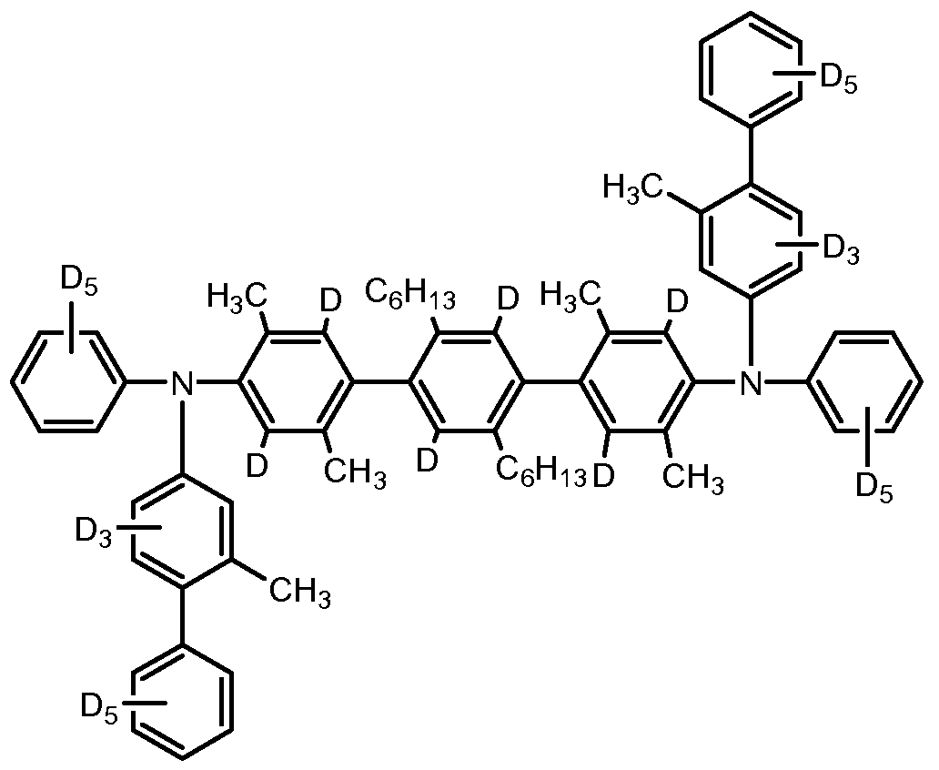
- the priming material is deuterated.
- deuterated is intended to mean that at least one H has been replaced by D.
- deuterated analog refers to a structural analog of a compound or group in which one or more available hydrogens have been replaced with deuterium. In a deuterated compound or deuterated analog, the deuterium is present in at least 100 times the natural abundance level. In some
- the priming material is at least 10% deuterated.
- % deuterated or “% deuteration” is meant the ratio of deuterons to the sum of protons plus deuterons, expressed as a percentage.
- the priming material is at least 20% deuterated; in some embodiments, at least 30% deuterated; in some embodiments, at least 40% deuterated; in some embodiments, at least 50% deuterated; in some embodiments, at least 60% deuterated; in some embodiments, at least 70% deuterated; in some embodiments, at least 80% deuterated; in some embodiments, at least 90% deuterated; in some embodiments, 100% deuterated.
- Deuterated priming materials can be less susceptible to degradation by holes, electrons, exitons, or a combination thereof. Deuteration can potentially inhibit degradation of the priming layer during device operation, which in turn can lead to improved device lifetime. In general, this
- the deuterated compounds frequently have greater air tolerance than the non-deuterated analogs. This can result in greater processing tolerance both for the preparation and purification of the materials and in the formation of electronic devices using the materials.
- the priming layer can be applied by any known deposition process. In one embodiment, the priming layer is applied without adding it to a solvent. In one embodiment, the priming layer is applied by vapor deposition.
- the priming layer is applied by a condensation process. If the priming layer is applied by condensation from the vapor phase, and the surface layer temperature is too high during vapor
- the priming layer can migrate into the pores or free volume of an organic substrate surface.
- the organic substrate is maintained at a temperature below the glass transition temperature or the melting temperature of the substrate materials.
- the temperature can be maintained by any known techniques, such as placing the first layer on a surface which is cooled with flowing liquids or gases.
- the priming layer is applied to a temporary support prior to the condensation step, to form a uniform coating of priming layer.
- This can be accomplished by any deposition method, including liquid deposition, vapor deposition, and thermal transfer.
- the priming layer is deposited on the temporary support by a continuous liquid deposition technique. The choice of liquid medium for depositing the priming layer will depend on the exact nature of the priming layer itself.
- the material is deposited by spin coating. The coated temporary support is then used as the source for heating to form the vapor for the condensation step.
- priming layer can be accomplished utilizing either continuous or batch processes. For instance, in a batch process, one or more devices would be coated simultaneously with the priming layer and then exposed simultaneously to a source of radiation. In a continuous process, devices transported on a belt or other conveyer device would pass a station when they are sequentially coated with priming layer and then continue past a station where they are sequentially exposed to a source of radiation. Portions of the process may be continuous while other portions of the process may be batch.
- the priming layer is deposited from a second liquid composition.
- the liquid deposition method can be continuous or
- the priming liquid composition is deposited using a continuous liquid deposition method.
- the choice of liquid medium for depositing the priming layer will depend on the exact nature of the priming material itself.
- the priming layer After the priming layer is formed, it is exposed to radiation.
- the type of radiation used will depend upon the sensitivity of the priming layer as discussed above.
- the exposure is patternwise. As used herein, the term "patternwise" indicates that only selected portions of a material or layer are exposed. Patternwise exposure can be achieved using any known imaging technique. In one embodiment, the pattern is achieved by exposing through a mask. In one embodiment, the pattern is achieved by exposing only select portions with a rastered laser. The time of exposure can range from seconds to minutes, depending upon the specific chemistry of the priming layer used. When lasers are used, much shorter exposure times are used for each individual area, depending upon the power of the laser.
- the exposure step can be carried out in air or in an inert atmosphere, depending upon the sensitivity of the materials.
- the radiation is selected from the group consisting of ultra-violet radiation (10-390 nm), visible radiation (390-770 nm), infrared radiation (770-10 6 nm), and combinations thereof, including simultaneous and serial treatments.
- the radiation is selected from visible radiation and ultraviolet radiation.
- the radiation has a wavelength in the range of 300 to 450 nm.
- the radiation is deep UV (200-300 nm).
- the ultraviolet radiation has a wavelength between 300 and 400 nm .
- the radiation has a wavelength in the range of 400 to 450 nm. In one
- the radiation is thermal radiation.
- the exposure to radiation is carried out by heating.
- the temperature and duration for the heating step is such that at least one physical property of the priming layer is changed, without damaging any underlying layers of the light-emitting areas.
- the heating temperature is less than 250°C. In one embodiment, the heating temperature is less than 150°C.
- the priming layer is developed. Development can be accomplished by any known technique. Such as
- development techniques have been used extensively in the photoresist and printing art.
- Examples of development techniques include, but are not limited to, application of heat (evaporation), treatment with a liquid medium (washing), treatment with an absorbant material (blotting), treatment with a tacky material, and the like.
- the development step results in effective removal of the priming layer in either the unexposed areas.
- the priming layer then remains in the exposed areas.
- the priming layer may also be partially removed in the exposed areas, but enough must remain in order for there to be a wettability difference between the exposed and unexposed areas.
- the exposure of the priming layer to radiation results in a change in the solubility or dispersibility of the priming layer in solvents.
- development can be accomplished by a wet
- the treatment usually involves washing with a solvent which dissolves, disperses or lifts off one type of area.
- the patternwise exposure to radiation results in ⁇ solubilization of the exposed areas of the priming layer, and treatment with solvent results in removal of the unexposed areas of the priming layer.
- the exposure of the priming layer to radiation results in a reaction which changes the volatility of the priming layer in exposed areas.
- development can be accomplished by a thermal development treatment.
- the treatment involves heating to a temperature above the volatilization or sublimation temperature of the more volatile material and below the temperature at which the material is thermally reactive.
- the material would be heated at a temperature above the sublimation temperature and below the thermal polymerization temperature.
- priming materials which have a temperature of thermal reactivity that is close to or below the volatilization temperature, may not be able to be developed in this manner.
- the exposure of the priming layer to radiation results in a change in the temperature at which the material melts, softens or flows.
- development can be accomplished by a dry development treatment.
- a dry development treatment can include contacting an outermost surface of the element with an absorbent surface to absorb or wick away the softer portions. This dry development can be carried out at an elevated temperature, so long as it does not further affect the properties of the remaining areas.
- the development step results areas of priming layer that remain and areas in which the underlying first layer is uncovered.
- the difference in contact angle with a given solvent for the patterned priming layer and uncovered areas is at least 20°; in some embodiments, at least 30°; in some embodiments, at least 40°.
- the second layer is then applied by liquid deposition over and on the developed pattern of priming material on the first layer.
- the second layer is a second organic active layer in an electronic device.
- the second layer can be applied by any liquid deposition technique.
- a liquid composition comprising a second material dissolved or dispersed in a liquid medium, is applied over the pattern of developed priming layer, and dried to form the second layer.
- the liquid composition is chosen to have a surface energy that is greater than the surface energy of the first layer, but approximately the same as or less than the surface energy of the developed priming layer.
- the liquid composition will wet the developed priming layer, but will be repelled from the first layer in the areas where the priming layer has been removed.
- the liquid may spread onto the treated first layer area, but it will de-wet and be contained to the pattern of the developed priming layer.
- the second layer is applied by a continuous liquid deposition technique, as described above.
- the first and second layers are organic active layers.
- the first organic active layer is formed over a first electrode
- a priming layer is formed over the first organic active layer, exposed to radiation and developed to form a pattern of developed priming layer
- the second organic active layer is formed over the developed priming layer on the first organic active layer, such that it is present only over and in the same pattern as the priming layer.
- the first organic active layer is formed by liquid deposition of a first liquid composition comprising the first organic active material and a first liquid medium.
- the liquid composition is deposited over the first electrode layer, and then dried to form a layer.
- the first organic active layer is formed by a continuous liquid deposition method. Such methods may result in higher yields and lower equipment costs.
- the priming is formed by liquid deposition of a second liquid composition comprising the priming material in a second liquid medium.
- the second liquid medium can be the same as or different from the first liquid medium, so long as it does not damage the first layer.
- the liquid deposition method can be continuous or discontinuous, as described above.
- the priming liquid composition is deposited using a continuous liquid deposition method.
- the second organic active layer is formed by liquid deposition of a third liquid composition comprising the second organic active material and a third liquid medium.
- the third liquid medium can be the same as or different from the first and second liquid media, so long as it does not damage the first layer or the developed priming layer.
- the second organic active layer is formed by printing.
- a third layer is applied over the second layer, such that it is present only over and in the same pattern as the second layer.
- the third layer can be applied by any of the processes described above for the second layer.
- the third layer is applied by a liquid deposition technique.
- the third organic active layer is formed by a printing method selected from the group consisting of ink jet printing and continuous nozzle printing.
- the priming material is the same as the second organic active material.
- the thickness of the developed priming layer can depend upon the ultimate end use of the material. In some embodiments, the developed priming layer is less than 100A in thickness. In some embodiments, the thickness is in the range of 1 -50A; in some embodiments 5-30A.
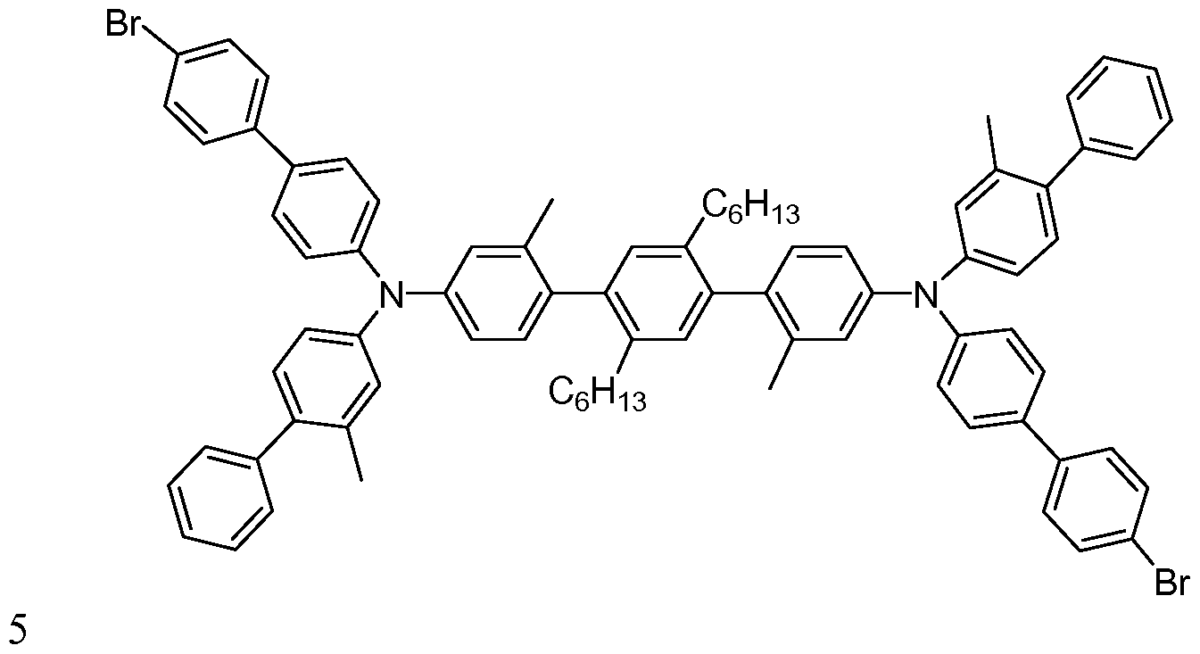
- the priming material has Formula I or Formula ⁇ :
- Ar 1 and Ar 2 are the same or different and are aryl groups
- R 1 through R 5 are independently the same or different at each
- R 6 is the same or different at each occurrence and is selected from the group consisting of H, D, and halogen;
- a through e are independently an integer from 0 to 4.
- f 1 or 2;
- g 0, 1 or 2;
- h is 1 or 2;
- n is an integer greater than 0.
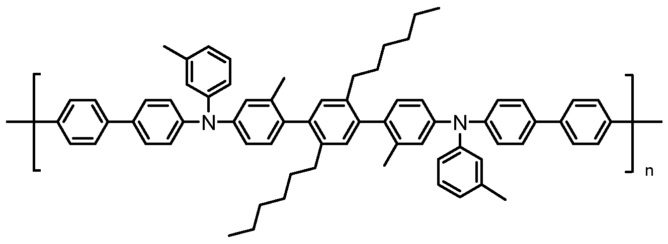
- the compound is a polymer with M n >20,000; in some embodiments, M n >50,000.
- the compound having Formula I or Formula ⁇ is deuterated.
- deuterated is intended to mean that at least one H has been replaced by D.
- deuterated analog refers to a structural analog of a compound or group in which one or more available hydrogens have been replaced with deuterium. In a deuterated compound or deuterated analog, the deuterium is present in at least 100 times the natural abundance level. In some embodiments, the compound is at least 10% deuterated.
- % deuterated or “% deuteration” is meant the ratio of deuterons to the sum of protons plus deuterons, expressed as a percentage. In some
- the compound is at least 20% deuterated; in some embodiments, at least 30% deuterated; in some embodiments, at least 40% deuterated; in some embodiments, at least 50% deuterated; in some embodiments, at least 60% deuterated; in some embodiments, at least 70% deuterated; in some embodiments, at least 80% deuterated; in some embodiments, at least 90% deuterated; in some embodiments, 100% deuterated.
- Deuterated materials can be less susceptible to degradation by holes, electrons, exitons, or a combination thereof. Deuteration can potentially inhibit degradation of the compound during device operation, which in turn can lead to improved device lifetime. In general, this improvement is accomplished without sacrificing other device properties. Furthermore, the deuterated compounds frequently have greater air tolerance than the non- deuterated analogs. This can result in greater processing tolerance both for the preparation and purification of the materials and in the formation of electronic devices using the materials.
- the compound of Formula I or Formula ⁇ has Formula la:
- R 1 through R 6 , Ar 1 , Ar 2 , a-h, and n are as defined above for Formula I.
- Ar 1 and Ar 2 are aryl groups having no fused rings. In some embodiments, Ar 1 and Ar 2 have Formula a
- R 7 is the same or different at each occurrence and is selected from the group consisting of D, alkyl, alkoxy, siloxane and silyl;
- n is an integer from 1 to 5.
- Ar 1 and Ar 2 have Formula b
- R 7 is the same or different at each occurrence and is selected from the group consisting of D, alkyl, alkoxy, siloxane and silyl;
- n is an integer from 1 to 5.
- Ar 1 and Ar 2 are selected from the group consisting of phenyl, biphenyl, terphenyl, deuterated derivatives thereof, and derivatives thereof having one or more substituents selected from the group consisting of alkyl, alkoxy, silyl, and a substituent with a crosslinking group.
- R 1 through R 5 are D or CMO alkyl. In some embodiments, the alkyl group is deuterated.
- R 1 and R 5 are D.
- the alkyl group is deuterated.
- d > 0 and at least one R 4 is alkyl.
- the alkyl group is deuterated.
- d 4, one R 4 is alkyl and the remainder are D.
- g 1 .
- the compounds having Formula I or Formula ⁇ have high triplet energies.
- triplet energy refers to the lowest excited triplet state of a material, in eV. Triplet energies are reported as positive numbers and represent the energy of the triplet state relative to the ground state, usually a singlet state.
- Luminescent organometallic materials emit from excited states having mixed singlet and triplet character and are referred to herein as "phosphorescent".
- the presence of materials having low triplet energy leads to quenching of phosphorescent emission of >2.0eV energy. This leads to decreased efficiency. Quenching can occur when the materials are in the electroluminescent layer, such as a host material, or in other layers in the device.
- the material having Formula I or Formula ⁇ has a triplet energy level greater than 2.1 eV; in some embodiments, greater than 2.2 eV; in some embodiments, greater than 2.45 eV; in some embodiments, greater than 2.6 eV.
- the triplet energy can either be calculated a priori, or be measured using pulse radiolysis or low temperature luminescence spectroscopy.
- Formula ⁇ include Compounds A through EE below.
- the new compounds can be made using any technique that will yield a C-C or C-N bond.
- a variety of such techniques are known, such as Suzuki, Yamamoto, Stille, and Pd- or Ni-catalyzed C-N couplings.
- Deuterated compounds can be prepared in a similar manner using deuterated precursor materials or, more generally, by treating the non-deuterated compound with deuterated solvent, such as d6-benzene, in the presence of a Lewis acid H/D exchange catalyst, such as aluminum trichloride or ethyl aluminum dichloride. Exemplary preparations are given in the Examples.
- the compounds can be formed into layers using solution processing techniques.
- layer is used interchangeably with the term “film” and refers to a coating covering a desired area.
- the term is not limited by size.
- the area can be as large as an entire device or as small as a specific functional area such as the actual visual display, or as small as a single sub- pixel.
- Layers and films can be formed by any conventional deposition technique, including vapor deposition, liquid deposition (continuous and discontinuous techniques), and thermal transfer.
- Continuous deposition techniques include but are not limited to, spin coating, gravure coating, curtain coating, dip coating, slot-die coating, spray coating, and continuous nozzle coating.
- Discontinuous deposition techniques include, but are not limited to, ink jet printing, gravure printing, and screen printing.
- FIG. 2 is an exemplary electronic device, an organic light-emitting diode (OLED) display that includes at least two organic active layers positioned between two electrical contact layers.
- the electronic device 100 includes one or more layers 120 and 130 to facilitate the injection of holes from the anode layer 1 10 into the emissive layer 140.
- the layer 120 adjacent the anode is called the hole injection layer, sometimes called a buffer layer.
- the layer 130 adjacent to the emissive layer is called the hole transport layer.
- An optional electron transport layer 150 is located between the emissive layer 140 and a cathode layer 160.
- the organic layers 120 through 150 are individually and
- the emissive layer 140 can be a light- emitting layer that is activated by an applied voltage (such as in a light- emitting diode or light-emitting electrochemical cell), a layer of material that responds to radiant energy and generates a signal with or without an applied bias voltage (such as in a photodetector).
- an applied voltage such as in a light- emitting diode or light-emitting electrochemical cell
- a layer of material that responds to radiant energy and generates a signal with or without an applied bias voltage (such as in a photodetector).
- the device is not limited with respect to system, driving method, and utility mode.
- the priming layer is not shown in this diagram.
- the emissive layer 140 is made up different areas of at least three different colors.
- the areas of different color can be formed by printing the separate colored areas. Alternatively, it can be accomplished by forming an overall layer and doping different areas of the layer with emissive materials with different colors. Such a process has been described in, for example, published U.S. patent application 2004-0094768.
- the new process described herein can be used for any successive pairs of organic layers in the device, where the second layer is to be contained in a specific area.
- the process for making an organic electronic device comprising an electrode having positioned thereover a first organic active layer and a second organic active layer, comprises:
- the first organic active layer having a first surface energy over the electrode
- priming material has Formula I or Formula ⁇ , as described above.
- the second organic active layer is the emissive layer 140
- the first organic active layer is the device layer applied just before layer 140.
- the device is constructed beginning with the anode layer.
- the priming layer would be applied to layer 130 and developed prior to applying the emissive layer 140.
- the priming layer would be applied to layer 120.
- the priming layer would be applied to the electron transport layer 150 prior to applying the emissive layer 140.
- the first organic active layer is the hole injection layer 120 and the second organic active layer is the hole transport layer 130.
- the priming layer is applied to hole injection layer 120 and developed prior to applying the hole transport layer 130.
- the hole injection layer comprises a fluorinated material.
- the hole injection layer comprises a conductive polymer doped with a fluorinated acid polymer.
- the hole injection layer consists essentially of a conductive polymer doped with a fluorinated acid polymer.
- the priming layer consists essentially of hole transport material.
- the priming layer consists essentially of the same hole transport material as the hole transport layer.
- Suitable materials include the mixed oxides of the Group 2 elements (i.e., Be, Mg, Ca, Sr, Ba), the Group 1 1 elements, the elements in Groups 4, 5, and 6, and the Group 8-10 transition elements. If the anode layer 1 10 is to be light transmitting, mixed oxides of Groups 12, 13 and 14 elements, such as indium-tin-oxide, may be used. As used herein, the phrase "mixed oxide” refers to oxides having two or more different cations selected from the Group 2 elements or the Groups 12, 13, or 14 elements.
- the anode layer 1 10 may be formed by a chemical or physical vapor deposition process or spin-cast process.
- Chemical vapor deposition may be performed as a plasma-enhanced chemical vapor deposition ("PECVD") or metal organic chemical vapor deposition ("MOCVD”).
- Physical vapor deposition can include all forms of sputtering, including ion beam sputtering, as well as e-beam evaporation and resistance evaporation.
- Specific forms of physical vapor deposition include rf magnetron sputtering and inductively- coupled plasma physical vapor deposition ("IMP-PVD"). These deposition techniques are well known within the semiconductor fabrication arts.
- the anode layer 1 10 is patterned during a lithographic operation.
- the pattern may vary as desired.
- the layers can be formed in a pattern by, for example, positioning a patterned mask or resist on the first flexible composite barrier structure prior to applying the first electrical contact layer material.
- the layers can be applied as an overall layer (also called blanket deposit) and subsequently patterned using, for example, a patterned resist layer and wet chemical or dry etching techniques. Other processes for patterning that are well known in the art can also be used.
- the anode layer 1 10 typically is formed into substantially parallel strips having lengths that extend in substantially the same direction.
- the hole injection layer 120 functions to facilitate injection of holes into the emissive layer and to planarize the anode surface to prevent shorts in the device.
- Hole injection materials may be polymers, oligomers, or small molecules, and may be in the form of solutions, dispersions, suspensions, emulsions, colloidal mixtures, or other compositions.
- the hole injection layer can be formed with polymeric materials, such as polyaniline (PANI) or polyethylenedioxythiophene (PEDOT), which are often doped with protonic acids.
- the protonic acids can be, for example, poly(styrenesulfonic acid), poly(2-acrylamido-2-methyl-1 -propanesulfonic acid), and the like.
- the hole injection layer 120 can comprise charge transfer compounds, and the like, such as copper phthalocyanine and the
- the hole injection layer 120 is made from a dispersion of a conducting polymer and a colloid-forming polymeric acid.
- a conducting polymer and a colloid-forming polymeric acid.
- Such materials have been described in, for example, published U.S. patent applications US 2004/0102577, US 2004/0127637, US 2005/0205860, and published PCT application WO 2009/018009.
- the hole injection layer 120 can be applied by any deposition technique.
- the hole injection layer is applied by a solution deposition method, as described above.
- the hole injection layer is applied by a continuous solution deposition method.
- hole transporting molecules include, but are not limited to: 4,4',4"-tris(N,N-diphenyl-amino)- triphenylamine (TDATA); 4,4',4"-tris(N-3-methylphenyl-N-phenyl-amino)- triphenylamine (MTDATA); N,N'-diphenyl-N,N'-bis(3-methylphenyl)-[1 ,1 '- biphenyl]-4,4'-diamine (TPD); 4, 4'-bis(carbazol-9-yl)biphenyl (CBP); 1 ,3- bis(carbazol-9-yl)benzene (mCP); 1 ,1 -bis[(di-4-tolylamino)
- TAPC phenyljcyclohexane
- EPD phenyljcyclohexane
- PDA tetrakis-(3- methylphenyl)-N,N,N',N'-2,5-phenylenediannine
- TPS p-(diethylamino)benzaldehyde
- TPA triphenylamine
- MPMP bis[4-(N,N-diethylamino)-2- methylphenyl](4-nnethylphenyl)nnethane
- MPMP bis[4-(N,N-diethylamino)-2- methylphenyl](4-nnethylphenyl)nnethane
- MPMP bis[4-(N,N-diethylamino)-2- methylphenyl](4-nnethylphenyl)nnethane
- PPR or DEASP 1 -phenyl-3-[p- (diethylamino)styryl]-5-[p-(diethylannino)phenyl] pyrazoline (PPR or DEASP); 1 ,2-trans-bis(9H-carbazol-9-yl)cyclobutane (DCZB); N,N,N',N'-tetrakis(4- methylphenyl)-(
- the hole transport layer comprises a hole transport polymer. In some embodiments, the hole transport layer consists essentially of a hole transport polymer. In some embodiments, the hole transport polymer is a distyrylaryl compound. In some embodiments, the aryl group is has two or more fused aromatic rings. In some embodiments, the aryl group is an acene.
- acene refers to a hydrocarbon parent component that contains two or more ortho-lused benzene rings in a straight linear arrangement.
- the hole transport polymer is an arylamine polymer. In some embodiments, it is a copolymer of fluorene and arylamine monomers.
- the polymer has crosslinkable groups.
- crosslinking can be accomplished by a heat treatment and/or exposure to UV or visible radiation.
- crosslinkable groups include, but are not limited to vinyl, acrylate, perfluorovinylether, 1 -benzo-3,4- cyclobutane, siloxane, and methyl esters.
- Crosslinkable polymers can have advantages in the fabrication of solution-process OLEDs. The application of a soluble polymeric material to form a layer which can be converted into an insoluble film subsequent to deposition, can allow for the fabrication of multilayer solution-processed OLED devices free of layer dissolution problems.
- crosslinkable polymers examples include crosslinkable polymers. Examples of crosslinkable polymers can be found in, for example, published US patent application 2005/0184287 and published PCT
- the copolymer is made from a third comonomer selected from (vinylphenyl)diphenylamine and 9,9-distyrylfluorene or 9,9- di(vinylbenzyl)fluorene.
- the hole transport layer comprises a material comprising triarylamines having conjugated moieties which are connected in a non-planar configuration. Such materials can be monomeric or polymeric. Examples of such materials have been described in, for example, published PCT application WO 2009/067419.
- the hole transport layer comprises a material having Formula I or Formula ⁇ , as described above. In some embodiments, the hole transport layer consists essentially of a material having Formula I or Formula ⁇ .
- the emissive layer 140 can be a light-emitting layer that is activated by an applied voltage (such as in a light-emitting diode or light-emitting electrochemical cell), a layer of material that responds to radiant energy and generates a signal with or without an applied bias voltage (such as in a photodetector).
- the emissive material is an organic electroluminescent ("EL") material. Any EL material can be used in the devices, including, but not limited to, small molecule organic fluorescent compounds, fluorescent and phosphorescent metal complexes, conjugated polymers, and mixtures thereof.
- fluorescent compounds include, but are not limited to, chrysenes, pyrenes, perylenes, rubrenes, coumarins, anthracenes, thiadiazoles, derivatives thereof, and mixtures thereof.
- metal complexes include, but are not limited to, metal chelated oxinoid compounds, such as tris(8- hydroxyquinolato)aluminum (Alq3); cyclometalated iridium and platinum electroluminescent compounds, such as complexes of iridium with
- phenylpyridine, phenylquinoline, or phenylpyrimidine ligands as disclosed in Petrov et al., U.S. Patent 6,670,645 and Published PCT Applications WO 03/063555 and WO 2004/016710, and organometallic complexes described in, for example, Published PCT Applications WO 03/008424, WO 03/091688, and WO 03/040257, and mixtures thereof.
- the small molecule fluorescent or organometallic materials are deposited as a dopant with a host material to improve processing and/or electronic properties.
- conjugated polymers include, but are not limited to poly(phenylenevinylenes), polyfluorenes, poly(spirobifluorenes), polythiophenes, poly(p-phenylenes), copolymers thereof, and mixtures thereof.
- the emissive layer 140 can be applied by any deposition technique.
- the emissive layer is applied by a solution deposition method, as described above.
- the emissive layer is applied by a continuous solution deposition method.
- Optional layer 150 can function both to facilitate electron transport, and also serve as a buffer layer or confinement layer to prevent quenching of the exciton at layer interfaces. Preferably, this layer promotes electron mobility and reduces exciton quenching.
- Examples of electron transport materials which can be used in the optional electron transport layer 150 include metal chelated oxinoid compounds, including metal quinolate derivatives such as tris(8-hydroxyquinolato)aluminum (AIQ), bis(2-methyl-8-quinolinolato)(p- phenylphenolato) aluminum (BAIq), tetrakis-(8-hydroxyquinolato)hafnium (HfQ) and tetrakis-(8-hydroxyquinolato)zirconium (ZrQ); and azole
- AIQ tris(8-hydroxyquinolato)aluminum
- BAIq bis(2-methyl-8-quinolinolato)(p- phenylphenolato) aluminum
- HfQ tetrakis-(8-hydroxyquinolato)hafnium
- ZrQ tetrakis-(8-hydroxyquinolato)zirconium
- the electron transport layer further comprises an n-dopant.
- N-dopant materials are well known.
- the electron transport layer 150 is usually formed by a chemical or physical vapor deposition process.
- the cathode 160 is an electrode that is particularly efficient for injecting electrons or negative charge carriers.
- the cathode can be any metal or nonmetal having a lower work function than the anode.
- Materials for the cathode can be selected from alkali metals of Group 1 (e.g., Li, Cs), the Group 2 (alkaline earth) metals, the Group 12 metals, including the rare earth elements and lanthanides, and the actinides. Materials such as aluminum, indium, calcium, barium, samarium and magnesium, as well as combinations, can be used.
- the cathode layer 160 is usually formed by a chemical or physical vapor deposition process.
- additional layers(s) may be present within organic electronic devices.
- each functional layer can be made up of more than one layer.
- the different layers have the following range of thicknesses: anode 1 10, 100-5000 A, in one embodiment 100-2000 A; hole injection layer 120, 50-2500 A, in one embodiment 200-1000 A; hole transport layer 130, 50-2500 A, in one embodiment 200-1000 A; emissive layer 140, 10-2000 A, in one embodiment 100-1000 A; electron transport layer 150, 50- 2000 A, in one embodiment 100-1000 A; cathode 160, 200-10000 A, in one embodiment 300-5000 A.
- the amount of material deposited is generally in the range of 1 -100 A, in one embodiment 1 -10 A.
- the desired ratio of layer thicknesses will depend on the exact nature of the materials used.
- a process for making an organic electronic device comprising an anode having thereon a hole injection layer and a hole transport layer, said process comprising:
- hole injection layer over the anode, said hole injection layer comprising a fluorinated material and having a first surface energy; forming a priming layer directly on the hole injection layer;
- the priming layer comprises a material having Formula I or Formula ⁇ , as described above.
- Device 200 has an anode 210 on a substrate (not shown). On the anode is hole injection layer 220. The developed priming layer is shown as 225. The surface energy of the hole injection layer 220 is less than the surface energy of the priming layer 225. When the hole transport layer 230 is deposited over the priming layer and hole injection layer, it does not wet the low energy surface of the hole injection layer and remains only over the pattern of the priming layer.
- the hole transport layer is selected from the group consisting of triarylamines, carbazoles, polymeric analogs thereof, and combinations thereof. In some embodiments, the hole transport layer is selected from the group consisting of polymeric triarylamines, polymeric triarylamines having conjugated moieties which are connected in a non- planar configuration, and copolymers of fluorene and triarylamines.
- Additional dibromo compounds can be prepared in an analogous manner. Additional polymers can be prepared from the dibromo
- Example 6 Compound T (20 nm)
- cathode CsF/AI (0.7/100 nm)
- OLED devices were fabricated by a combination of solution processing and thermal evaporation techniques.
- a patterned indium tin oxide (ITO) coated glass substrate from Thin Film Devices, Inc was used.
- the ITO substrate is based on Corning 1737 glass coated with ITO having a sheet resistance of 30 ohms/square and 80% light transmission.
- the patterned ITO substrate was cleaned ultrasonically in aqueous detergent solution and rinsed with distilled water. The patterned ITO was subsequently cleaned
Abstract
Description


Claims


Priority Applications (5)
| Application Number | Priority Date | Filing Date | Title |
|---|---|---|---|
| KR1020137001141A KR20130098984A (en) | 2010-06-17 | 2011-06-16 | Process and materials for making contained layers and devices made with same |
| CN201180027968.8A CN102934029B (en) | 2010-06-17 | 2011-06-16 | For the preparation of the method for included layer and material and the device be made up of it |
| JP2013515506A JP2013534026A (en) | 2010-06-17 | 2011-06-16 | Confinement layer and methods and materials for manufacturing devices manufactured using the same |
| EP11729510.5A EP2583139A2 (en) | 2010-06-17 | 2011-06-16 | Process and materials for making contained layers and devices made with same |
| US13/704,003 US20130087779A1 (en) | 2010-06-17 | 2011-06-16 | Process and materials for making contained layers and devices made with same |
Applications Claiming Priority (2)
| Application Number | Priority Date | Filing Date | Title |
|---|---|---|---|
| US35561710P | 2010-06-17 | 2010-06-17 | |
| US61/355,617 | 2010-06-17 |
Publications (2)
| Publication Number | Publication Date |
|---|---|
| WO2011159876A2 true WO2011159876A2 (en) | 2011-12-22 |
| WO2011159876A3 WO2011159876A3 (en) | 2012-03-15 |
Family
ID=44627906
Family Applications (1)
| Application Number | Title | Priority Date | Filing Date |
|---|---|---|---|
| PCT/US2011/040657 WO2011159876A2 (en) | 2010-06-17 | 2011-06-16 | Process and materials for making contained layers and devices made with same |
Country Status (7)
| Country | Link |
|---|---|
| US (1) | US20130087779A1 (en) |
| EP (1) | EP2583139A2 (en) |
| JP (1) | JP2013534026A (en) |
| KR (1) | KR20130098984A (en) |
| CN (1) | CN102934029B (en) |
| TW (1) | TW201200975A (en) |
| WO (1) | WO2011159876A2 (en) |
Cited By (3)
| Publication number | Priority date | Publication date | Assignee | Title |
|---|---|---|---|---|
| JP2015508568A (en) * | 2011-12-22 | 2015-03-19 | サイノーラ・ゲゼルシャフト・ミト・ベシュレンクテル・ハフツング | Organic molecules for OLEDs and other optoelectronic devices |
| EP4071193A4 (en) * | 2020-03-27 | 2023-09-13 | Lg Chem, Ltd. | Novel polymer and organic light-emitting element comprising same |
| EP4145546A4 (en) * | 2020-08-06 | 2023-11-08 | Lg Chem, Ltd. | Organic light-emitting device |
Families Citing this family (7)
| Publication number | Priority date | Publication date | Assignee | Title |
|---|---|---|---|---|
| EP2459379A4 (en) * | 2009-07-27 | 2015-05-06 | Du Pont | Process and materials for making contained layers and devices made with same |
| TW201204687A (en) * | 2010-06-17 | 2012-02-01 | Du Pont | Electroactive materials |
| KR102157997B1 (en) * | 2013-10-04 | 2020-09-21 | 미쯔비시 케미컬 주식회사 | Polymer, composition for organic electroluminescent element, organic electroluminescent element, organic el display device, and organic el lighting |
| US9525134B1 (en) * | 2015-08-11 | 2016-12-20 | E I Du Pont De Nemours And Company | Hole transport materials |
| TWI786143B (en) * | 2017-07-03 | 2022-12-11 | 德商麥克專利有限公司 | Organic electroluminescent device and method for producing the same |
| US20220005687A1 (en) * | 2020-07-02 | 2022-01-06 | Taiwan Semiconductor Manufacturing Company, Ltd. | Method of manufacturing a semiconductor device and pattern formation method |
| JP2023526683A (en) * | 2020-08-06 | 2023-06-22 | エルジー・ケム・リミテッド | organic light emitting device |
Citations (14)
| Publication number | Priority date | Publication date | Assignee | Title |
|---|---|---|---|---|
| WO2003008424A1 (en) | 2001-07-18 | 2003-01-30 | E.I. Du Pont De Nemours And Company | Luminescent lanthanide complexes with imine ligands and devices made with such complexes |
| WO2003040257A1 (en) | 2001-11-07 | 2003-05-15 | E. I. Du Pont De Nemours And Company | Electroluminescent platinum compounds and devices made with such compounds |
| WO2003063555A1 (en) | 2001-12-26 | 2003-07-31 | E. I. Du Pont De Nemours And Company | Electroluminescent iridium compounds wiht fluorinated phenylpyridines, phenylpyrimidines, and phenylquinolines and devices made with such compounds |
| WO2003091688A2 (en) | 2001-07-05 | 2003-11-06 | E.I. Du Pont De Nemours And Company | Photoactive lanthanide complexes with phosphine oxides, phosphine oxide-sulfides, pyridine n-oxides, and phosphine oxide-pyridine n-oxides, and devices made with such complexes |
| US6670645B2 (en) | 2000-06-30 | 2003-12-30 | E. I. Du Pont De Nemours And Company | Electroluminescent iridium compounds with fluorinated phenylpyridines, phenylpyrimidines, and phenylquinolines and devices made with such compounds |
| WO2004016710A1 (en) | 2002-08-15 | 2004-02-26 | E.I. Du Pont De Nemours And Company | Compounds comprising phosphorus-containing metal complexes |
| US20040094768A1 (en) | 2002-09-06 | 2004-05-20 | Gang Yu | Methods for producing full-color organic electroluminescent devices |
| US20040102577A1 (en) | 2002-09-24 | 2004-05-27 | Che-Hsiung Hsu | Water dispersible polythiophenes made with polymeric acid colloids |
| US20040127637A1 (en) | 2002-09-24 | 2004-07-01 | Che-Hsiung Hsu | Water dispersible polyanilines made with polymeric acid colloids for electronics applications |
| WO2005052027A1 (en) | 2003-11-17 | 2005-06-09 | Sumitomo Chemical Company, Limited | Crosslinkable arylamine compounds and conjugated oligomers of polymers based thereon |
| US20050184287A1 (en) | 2004-02-20 | 2005-08-25 | Norman Herron | Cross-linkable polymers and electronic devices made with such polymers |
| US20050205860A1 (en) | 2004-03-17 | 2005-09-22 | Che-Hsiung Hsu | Water dispersible polypyrroles made with polymeric acid colloids for electronics applications |
| WO2009018009A1 (en) | 2007-07-27 | 2009-02-05 | E. I. Du Pont De Nemours And Company | Aqueous dispersions of electrically conducting polymers containing inorganic nanoparticles |
| WO2009067419A1 (en) | 2007-11-19 | 2009-05-28 | E. I. Du Pont De Nemours And Company | Electroactive materials |
Family Cites Families (5)
| Publication number | Priority date | Publication date | Assignee | Title |
|---|---|---|---|---|
| CN100572495C (en) * | 2002-03-09 | 2009-12-23 | Cdt牛津有限公司 | Polymerisable compound and the organic luminescent device that contains it |
| DE102004009355A1 (en) * | 2004-02-26 | 2005-09-15 | Covion Organic Semiconductors Gmbh | Process for crosslinking organic semiconductors |
| JP2009087781A (en) * | 2007-09-28 | 2009-04-23 | Dainippon Printing Co Ltd | Electroluminescent element and its manufacturing method |
| JP5155085B2 (en) * | 2008-10-01 | 2013-02-27 | 住友化学株式会社 | Organic electroluminescence device and method for manufacturing the same |
| EP2459379A4 (en) * | 2009-07-27 | 2015-05-06 | Du Pont | Process and materials for making contained layers and devices made with same |
-
2011
- 2011-06-15 TW TW100120846A patent/TW201200975A/en unknown
- 2011-06-16 WO PCT/US2011/040657 patent/WO2011159876A2/en active Application Filing
- 2011-06-16 KR KR1020137001141A patent/KR20130098984A/en not_active Application Discontinuation
- 2011-06-16 EP EP11729510.5A patent/EP2583139A2/en not_active Withdrawn
- 2011-06-16 US US13/704,003 patent/US20130087779A1/en not_active Abandoned
- 2011-06-16 CN CN201180027968.8A patent/CN102934029B/en active Active
- 2011-06-16 JP JP2013515506A patent/JP2013534026A/en active Pending
Patent Citations (14)
| Publication number | Priority date | Publication date | Assignee | Title |
|---|---|---|---|---|
| US6670645B2 (en) | 2000-06-30 | 2003-12-30 | E. I. Du Pont De Nemours And Company | Electroluminescent iridium compounds with fluorinated phenylpyridines, phenylpyrimidines, and phenylquinolines and devices made with such compounds |
| WO2003091688A2 (en) | 2001-07-05 | 2003-11-06 | E.I. Du Pont De Nemours And Company | Photoactive lanthanide complexes with phosphine oxides, phosphine oxide-sulfides, pyridine n-oxides, and phosphine oxide-pyridine n-oxides, and devices made with such complexes |
| WO2003008424A1 (en) | 2001-07-18 | 2003-01-30 | E.I. Du Pont De Nemours And Company | Luminescent lanthanide complexes with imine ligands and devices made with such complexes |
| WO2003040257A1 (en) | 2001-11-07 | 2003-05-15 | E. I. Du Pont De Nemours And Company | Electroluminescent platinum compounds and devices made with such compounds |
| WO2003063555A1 (en) | 2001-12-26 | 2003-07-31 | E. I. Du Pont De Nemours And Company | Electroluminescent iridium compounds wiht fluorinated phenylpyridines, phenylpyrimidines, and phenylquinolines and devices made with such compounds |
| WO2004016710A1 (en) | 2002-08-15 | 2004-02-26 | E.I. Du Pont De Nemours And Company | Compounds comprising phosphorus-containing metal complexes |
| US20040094768A1 (en) | 2002-09-06 | 2004-05-20 | Gang Yu | Methods for producing full-color organic electroluminescent devices |
| US20040102577A1 (en) | 2002-09-24 | 2004-05-27 | Che-Hsiung Hsu | Water dispersible polythiophenes made with polymeric acid colloids |
| US20040127637A1 (en) | 2002-09-24 | 2004-07-01 | Che-Hsiung Hsu | Water dispersible polyanilines made with polymeric acid colloids for electronics applications |
| WO2005052027A1 (en) | 2003-11-17 | 2005-06-09 | Sumitomo Chemical Company, Limited | Crosslinkable arylamine compounds and conjugated oligomers of polymers based thereon |
| US20050184287A1 (en) | 2004-02-20 | 2005-08-25 | Norman Herron | Cross-linkable polymers and electronic devices made with such polymers |
| US20050205860A1 (en) | 2004-03-17 | 2005-09-22 | Che-Hsiung Hsu | Water dispersible polypyrroles made with polymeric acid colloids for electronics applications |
| WO2009018009A1 (en) | 2007-07-27 | 2009-02-05 | E. I. Du Pont De Nemours And Company | Aqueous dispersions of electrically conducting polymers containing inorganic nanoparticles |
| WO2009067419A1 (en) | 2007-11-19 | 2009-05-28 | E. I. Du Pont De Nemours And Company | Electroactive materials |
Non-Patent Citations (3)
| Title |
|---|
| "CRC Handbook of Chemistry and Physics", 2000 |
| DAVID BRAUN, ALAN J. HEEGER, APPL. PHYS. LETTERS, vol. 58, 1991, pages 1982 |
| Y. WANG: "Kirk-Othmer Encyclopedia of Chemical Technology", vol. 18, 1996, pages: 837 - 860 |
Cited By (3)
| Publication number | Priority date | Publication date | Assignee | Title |
|---|---|---|---|---|
| JP2015508568A (en) * | 2011-12-22 | 2015-03-19 | サイノーラ・ゲゼルシャフト・ミト・ベシュレンクテル・ハフツング | Organic molecules for OLEDs and other optoelectronic devices |
| EP4071193A4 (en) * | 2020-03-27 | 2023-09-13 | Lg Chem, Ltd. | Novel polymer and organic light-emitting element comprising same |
| EP4145546A4 (en) * | 2020-08-06 | 2023-11-08 | Lg Chem, Ltd. | Organic light-emitting device |
Also Published As
| Publication number | Publication date |
|---|---|
| CN102934029A (en) | 2013-02-13 |
| JP2013534026A (en) | 2013-08-29 |
| TW201200975A (en) | 2012-01-01 |
| WO2011159876A3 (en) | 2012-03-15 |
| EP2583139A2 (en) | 2013-04-24 |
| CN102934029B (en) | 2015-11-25 |
| US20130087779A1 (en) | 2013-04-11 |
| KR20130098984A (en) | 2013-09-05 |
Similar Documents
| Publication | Publication Date | Title |
|---|---|---|
| US9306185B2 (en) | Process and materials for making contained layers and devices made with same | |
| JP5871949B2 (en) | Confinement layer and methods and materials for manufacturing devices manufactured using the same | |
| US20130087779A1 (en) | Process and materials for making contained layers and devices made with same | |
| KR101516813B1 (en) | Organic electronic devices | |
| US9293739B2 (en) | Process and materials for making contained layers and devices made with same | |
| US8907353B2 (en) | Process for forming an electroactive layer | |
| JP5848362B2 (en) | Confinement layer and methods and materials for manufacturing devices manufactured using the same | |
| US9312485B2 (en) | Process and materials for making contained layers and devices made with same |
Legal Events
| Date | Code | Title | Description |
|---|---|---|---|
| WWE | Wipo information: entry into national phase |
Ref document number: 201180027968.8 Country of ref document: CN |
|
| 121 | Ep: the epo has been informed by wipo that ep was designated in this application |
Ref document number: 11729510 Country of ref document: EP Kind code of ref document: A2 |
|
| WWE | Wipo information: entry into national phase |
Ref document number: 2011729510 Country of ref document: EP |
|
| WWE | Wipo information: entry into national phase |
Ref document number: 13704003 Country of ref document: US |
|
| ENP | Entry into the national phase |
Ref document number: 2013515506 Country of ref document: JP Kind code of ref document: A |
|
| NENP | Non-entry into the national phase |
Ref country code: DE |
|
| ENP | Entry into the national phase |
Ref document number: 20137001141 Country of ref document: KR Kind code of ref document: A |